Capacitive Structures for Gas and Biological...
116
Capacitive Structures for Gas and Biological Sensing Thesis by Christos Sapsanis In Partial Fulfillment of the Requirements For the Degree of Master of Science King Abdullah University of Science and Technology Thuwal, Kingdom of Saudi Arabia March 2015
Transcript of Capacitive Structures for Gas and Biological...
Capacitive Structures for Gas and
Biological Sensing
Thesis by
Christos Sapsanis
In Partial Fulfillment of the Requirements
For the Degree of
Master of Science
King Abdullah University of Science and Technology
Thuwal, Kingdom of Saudi Arabia
March 2015

2
EXAMINATION COMMITTEE APPROVALS FORM
The thesis of Christos Sapsanis is approved by the examination committee.
Committee Chairperson: Dr. Khaled Salama
Committee Member: Dr. Jürgen Kosel
Committee Member: Dr. Boon S. Ooi

3
COPYRIGHT PAGE
© 2015
Christos Sapsanis
All Rights Reserved

4
ABSTRACT
Capacitive Structures for Gas and Biological Sensing
Christos Sapsanis
The semiconductor industry has been benefited by the technological advances in
the last decades. This fact has had an impact on the sensors field, where the simple
transducer has been evolved into smart miniaturized multi-functional microsystem.
However, commercially available gas and biological sensors are mostly bulky,
expensive and power-hungry, which act as obstacles for mass use. Thus, the
exponential growth of research in this area is fuelled by the need for inexpensive,
low-power and miniaturized sensors that can be fully integrated in microsystems and
compatible with lab-on-chip applications.
The aim of this thesis is to use capacitive structures for gas and biological
sensing. Capacitive sensors were selected due to its design simplicity, low fabrication
cost and no DC power consumption. In the first part, the dominant structure among
interdigitated electrodes (IDEs), fractal curves (Peano and Hilbert) and Archimedean
spiral was investigated from capacitance density perspective. The investigation
consists of geometrical formula calculations, COMSOL Multiphysics simulations and
cleanroom fabrication of the capacitors on silicon substrate to prove the dominance
of IDEs. Moreover, a low-cost fabrication on flexible plastic PET substrate was
conducted outside cleanroom using maskless laser etching.
The second part contains the humidity, Volatile Organic compounds (VOCs) and
Ammonia sensing of polymers, Polyimide and Nafion and metal-organic framework
(MOF), Cu(bdc).xH2O using IDEs. The Nafion has shown higher sensitivity compared
to Cu(bdc).xH2O in all the vapors testing and Polyimide had a linear response to
humidity testing. The need for a reliable and stable measuring system led in the

5
implementation of an automated gas setup for relative humidity, VOCs vapors and
toxic gases by employing LabVIEW software. The instruments of the setup were
controlled for automated experiments, data and curves extraction.
The last part includes the biological sensing. The first experiment deals with C -
reactive protein (CRP) quantification, which is considered as a biomarker of being
prone to cardiac diseases. The other experiment focuses on the Bovine serum albumin
(BSA) protein quantification, which is used as a reference for quantifying unknown
proteins. It was proven experimentally, that the capacitive sensors coated with
Parylene-C can quantify the utilized CRP and BSA concentrations.
6
ACKNOWLEDGEMENTS
I would like sincerely to thank my supervisor Prof. Khaled Salama for his support
and guidance throughout my master’s thesis and degree in general and for his
valuable advice for my later career goals.
I would like to expand my thanks to the committee members Prof. Jürgen Kosel
and Prof. Boon S. Ooi for taking out the time to attend my defense and to review my
thesis.
It would be an omission not to thank Prof. Eddaoudi and his group members, PhD
student Valeriya Chernikova and Dr. Osama Shekhah for the MOF film preparation
and Dr. Youssef Belmabkhout for providing the know-how for designing the gas setup.
I would also like to thank all the Sensor lab members and especially, Ph.D.
student Hesham Omran, Dr. Shilpa Sivashankar for their assistance in the gas and
biological sensing respectively. I owe Mr. Ulrich Buttner and Mr. Ahad Syed my
thanks for their practical solutions in problems occurred throughout my thesis.
Moreover, I want to thank the Internship student Faisal Alqarni and PhD students
Shuai Yang, Muhammad Farooqui, Hanan Mohammed for their assistance.
My appreciation also goes to the few but real friends at King Abdullah University
of Science and Technology for their support and the great experience we had the
opportunity to live there.
Last but not least, I would like to give special thank my family because I would
have done nothing without their continuous support and encouragement in all the
years of my studies and my life in general.
This work was partially sponsored by the Advanced Membranes and
Porous Materials Center (AMPMC)'s grant FCC/1/1972-05-01 within the ‘Stimuli
Responsive Materials’ thrust headed by Prof. N. Khashab
7
TABLE OF CONTENTS
EXAMINATION COMMITTEE APPROVALS FORM .............................................. 2
COPYRIGHT PAGE ..................................................................................................... 3
ABSTRACT ................................................................................................................... 4
ACKNOWLEDGEMENTS ........................................................................................... 6
TABLE OF CONTENTS ............................................................................................... 7
LIST OF ABBREVIATIONS ........................................................................................ 9
LIST OF ILLUSTRATIONS ....................................................................................... 10
LIST OF TABLES ....................................................................................................... 13
Chapter 1: Introduction ............................................................................................ 15
1.1 Motivation and background .......................................................................... 15
1.2 Market size and forecast ................................................................................ 16
1.3 Thesis Outline ............................................................................................... 18
Chapter 2: Capacitive Sensors ................................................................................. 20
2.1 Concept of Capacitance ................................................................................. 20
2.2 Geometrical Formula Calculations................................................................ 22
2.2.1 Interdigitated Electrodes (IDEs) ............................................................ 22
2.2.2 Archimedean Spiral ............................................................................... 24
2.2.3 Fractal Capacitors .................................................................................. 25
2.3 Simulations .................................................................................................... 30
2.4 Cleanroom fabrication ................................................................................... 36
2.5 Low-cost fabrication on PET substrate ......................................................... 43
2.5.1 Flexible Materials Characterization ....................................................... 43
2.5.2 Capacitive structures fabrication on PET .............................................. 44
Chapter 3: Gas Sensing ............................................................................................ 48
3.1 Gas Testing Setup.......................................................................................... 48
3.1.1 LabVIEW Automation ........................................................................... 52
3.2 Sensitive film materials ................................................................................. 53
3.2.1 Metal Oxide Semiconductors (MOS) .................................................... 54
3.2.2 Carbon nanomaterials ............................................................................ 55
3.2.3 Metal-Organic Frameworks (MOFs) ..................................................... 58
3.2.4 Polymers ................................................................................................ 61
3.2.5 Discussion .............................................................................................. 62
3.3 Breath sensors ............................................................................................... 63
3.4 Commercial applications ............................................................................... 66
3.5 Gas sensing experiments ............................................................................... 68
3.5.1 Utilized sensing films ............................................................................ 68

8
3.5.2 Relative Humidity Experiments ............................................................. 71
3.5.3 Volatile Organic Compounds and Ammonia Experiments ................... 76
3.5.4 Discussion .............................................................................................. 81
Chapter 4: Biological sensing .................................................................................. 85
4.1 Capacitive immunosensor to quantify C-reactive protein ............................. 86
4.2 Streptavidin - biotinylated BSA quantification ............................................. 90
Chapter 5: Conclusion and future work ................................................................... 93
Appendix ...................................................................................................................... 95
Data acquisition with automatic curve extraction .................................................... 95
LCR (Agilent 4980A) .......................................................................................... 95
Multimeter (Agilent 34401A) .............................................................................. 97
Curves extraction ................................................................................................. 98
Experiment automation with MFCs, chiller and hot plate control ........................... 99
RS232 Communication ...................................................................................... 100
Hot plate (Torrey Pines Scientific EcoTherm HS60) ........................................ 102
Chiller (Julabo F12-MA) ................................................................................... 104
Temperature sensor (LM35) .............................................................................. 105
Mass Flow Controllers (Alicat) ......................................................................... 106
Experiment Automation ..................................................................................... 108
References .................................................................................................................. 111
9
LIST OF ABBREVIATIONS
BSA bovine serum albumin
CD carrier detect
CRP C - reactive protein
CTS clear to send
DCE data communication equipment
DTE data terminal equipment
DTR data terminal ready
DSR data set ready
IDEs interdigitated electrodes
LCR inductance capacitance resistance
MFC mass flow controller
MFM mass flow meter
MOF metal–organic framework
PCV percentage capacitance variation
PET polyethylene terephthalate
PPC parallel plate capacitor
PVD physical vapor deposition
RH relative humidity
RI ring indicator
RTS request to send
SSCM standard cubic centimeters per minute
VI virtual instrument (LabVIEW)
VOC volatile organic compound
10
LIST OF ILLUSTRATIONS
Figure 1-1: Worldwide sensor market and unit shipments from 2008 to 2016 [6]...... 16 Figure 1-2: Global gas sensor market estimate and forecast for 2010 – 2018 [7] ....... 17 Figure 1-3: Global Gas sensors market by type in 2012 [8] ........................................ 17 Figure 1-4: Global biosensors market estimate and forecast for 2009 -2016 .............. 18
Figure 1-5: Global Biosensors market by area in 2016 ............................................... 18 Figure 2-1: Parallel plate capacitor .............................................................................. 20 Figure 2-2: (a) Vertical and (b) Lateral Flux Capacitor ............................................... 21 Figure 2-3: 3D Interdigitated electrodes (IDEs) .......................................................... 23 Figure 2-4: IDE cell in 2d ............................................................................................ 23
Figure 2-5: Archimedean Spiral................................................................................... 24
Figure 2-6: Creation of Peano’s curve higher orders ................................................... 26
Figure 2-7: Normal Peano Curve Cell ......................................................................... 27 Figure 2-8: Curvature Peano Curve Cell ..................................................................... 27 Figure 2-9: Creation of Hilbert’s curve higher orders ................................................. 28 Figure 2-10: Normal Hilbert Cell ................................................................................ 28 Figure 2-11: Curvature Hilbert Cell ............................................................................. 28
Figure 2-12: Ratio vs scale diagram ............................................................................ 29 Figure 2-13: Air filling approaches .............................................................................. 31
Figure 2-14: Simulated IDEs cell ................................................................................ 31 Figure 2-15: Simulated Spiral cell ............................................................................... 31
Figure 2-16: Simulated Peano N cell ........................................................................... 32 Figure 2-17: Simulated Peano C cell ........................................................................... 32
Figure 2-18: Simulated Hilbert N cell ......................................................................... 32 Figure 2-19: Simulated Hilbert C cell .......................................................................... 32
Figure 2-20: Capacitance vs scale for simulation type (c) ........................................... 33 Figure 2-21: Capacitance density vs scale for simulation type (c) .............................. 34 Figure 2-22: Parallel capacitors constituting the overall capacitance .......................... 35
Figure 2-23: Fabricated capacitor cell ......................................................................... 37 Figure 2-24: Fabrication process of the capacitive structures ..................................... 37
Figure 2-25: Fabricated IDEs in 2D............................................................................. 40 Figure 2-26: Fabricated IDEs in 3D............................................................................. 40 Figure 2-27: Fabricated Peano curve in 2D ................................................................. 41
Figure 2-28: Fabricated Peano curve in 3D ................................................................. 41 Figure 2-29: Fabricated Hilbert curve in 2D ................................................................ 41
Figure 2-30: Fabricated Hilbert curve in 3D ................................................................ 41 Figure 2-31: Fabricated Spiral in 2D ........................................................................... 41
Figure 2-32: Fabricated Spiral in 3D ........................................................................... 41 Figure 2-33: Capacitance vs scale for 512s x 512s ...................................................... 42 Figure 2-34: Capacitance density vs scale for 512s x 512s ......................................... 42 Figure 2-35: Relative Permittivity and Loss Tangent values for PET ......................... 44 Figure 2-36: Fabrication steps ..................................................................................... 45
Figure 2-37: (a) Removal of Au, (b) Au Peel off, (c) Short Circuit ............................ 46 Figure 2-38: (a) Fractal and (b) IDEs fabricated capacitors, (c) Flexibility ................ 46 Figure 2-39: (a) Optical microscope image of IDE structure; (b) enlarged image. ..... 46 Figure 2-40: (a) Optical microscope image of Hilbert structure; (b) enlarged image. 47 Figure 3-1: Setup configuration design ........................................................................ 49
Figure 3-2: Bubbler ...................................................................................................... 50
Figure 3-3: Testing chamber ........................................................................................ 50
11
Figure 3-4: Implemented testing setup ........................................................................ 52 Figure 3-5: Front Panel of data acquisition with curves extraction ............................. 53 Figure 3-6: Front Panel of Experiment automation ..................................................... 53 Figure 3-7: Chemical and Geometrical Representation of MOF-5 ............................. 60 Figure 3-8: Layer by layer approach for MOFs Fabrication ........................................ 60
Figure 3-9: CO2 detector by Greystone ....................................................................... 67 Figure 3-10: VOCs detector by RAE ........................................................................... 67 Figure 3-11: VOCs detector by ION ............................................................................ 67 Figure 3-12: Gas Watch 2 by RKI ............................................................................... 67 Figure 3-13: Multi gas detector by RAE...................................................................... 67
Figure 3-14: Gas Sensor MQ-2 .................................................................................... 67 Figure 3-15: Representation of Imide monomer chemical structure ........................... 69
Figure 3-16: Representation of Nafion’s Chemical structure ...................................... 69 Figure 3-17: Chemical Representation of the 2D Cu(bdc).xH2O MOF structure. ...... 70 Figure 3-18: XRPD of Cu(BDC).xH2O MOF thin film .............................................. 71 Figure 3-19: SEM of Cu(bdc).xH2O film .................................................................... 71 Figure 3-20: Ramp and Purge Experiment for HIH-4000 Sensor ............................... 71
Figure 3-21: Capacitance vs humidity plot using Polyimide ....................................... 72 Figure 3-22: Capacitance vs humidity plot using Nafion ............................................ 73
Figure 3-23: Results Reproducibility of Nafion Film For purging Experiment .......... 73 Figure 3-24: Capacitance vs humidity plot using Cu(bdc).xH2O MOF ...................... 74
Figure 3-25: Results Reproducibility of Cu(bdc).xH2O Film ...................................... 75 Figure 3-26: Part connecting the sensor with the LCR terminals ................................ 75 Figure 3-27: Capacitance vs RH plot for all the flexible sensors ................................ 76
Figure 3-28: Vapor generation process ........................................................................ 77
Figure 3-29: Nafion response to acetone, ethanol and methanol concentrations ........ 79 Figure 3-30: Nafion response to toluene and ammonia concentrations ....................... 79 Figure 3-31: MOF response to acetone, ethanol and methanol concentrations ........... 80
Figure 3-32: MOF response to toluene and ammonia concentrations ......................... 81 Figure 4-1: Agglutination process: immobilization of (a) antibodies, (b) antigens ..... 88
Figure 4-2: Agglutination progressing with time compared to the Capacitance vs Time
diagram ........................................................................................................................ 89 Figure 4-3: Relative Permittivity vs Antigen concentration ........................................ 89
Figure 4-4: Protocol for streptavidin immobilization .................................................. 91 Figure 4-5: Results for Protein specificity ................................................................... 91
Figure 4-6: Results for Protein quantification ............................................................. 92
Figure 0-1: Graph for selecting the most accurate model [109] .................................. 95
Figure 0-2: LCR control in Front Panel ....................................................................... 96 Figure 0-3: LCR initialization ...................................................................................... 96 Figure 0-4: AC and DC applied signal option ............................................................. 96 Figure 0-5: Multimeter control in Front panel ............................................................. 97 Figure 0-6: Multimeter in Block diagram .................................................................... 97
Figure 0-7: LabVIEW code for Accuracy and averaging ............................................ 98 Figure 0-8: XY graphs for plotting capacitance vs humidity curves ........................... 98 Figure 0-9: Clean Charts .............................................................................................. 99 Figure 0-10: Extract data to Excel files with Boolean option ...................................... 99 Figure 0-11: Hot plate’s Front Panel ......................................................................... 102
Figure 0-12: Hot plate and timer initialization .......................................................... 102
Figure 0-13: Target temperature command ............................................................... 102 Figure 0-14: Ramp command .................................................................................... 103
12
Figure 0-15: Current temperature command.............................................................. 103 Figure 0-16: Time command and check for terminating the loop ............................. 104 Figure 0-17: Chiller control block diagram ............................................................... 104 Figure 0-18: Chiller control Front Panel .................................................................... 105 Figure 0-19: Chiller experiment Front Panel ............................................................. 105
Figure 0-20: Chiller experiment block diagram......................................................... 105 Figure 0-21: LM35 front panel .................................................................................. 106 Figure 0-22: LM35 block diagram ............................................................................. 106 Figure 0-23: Front panel for Alicat MFC Control ..................................................... 107 Figure 0-24: Block diagram for Alicat MFC Control A & B .................................... 107
Figure 0-25: Block diagram for Alicat MFC Control D (same as C) and MFM E.... 107 Figure 0-26: Block diagram for turning off all the MFC’s in case of emergency ..... 107
Figure 0-27: Front panel for MFC Control subvi ...................................................... 108 Figure 0-28: Block diagram for MFC Control subvi ................................................. 108 Figure 0-29: (a) Purge, (b) Ramp and (c) Reverse experiment of HIH-4000 ............ 109 Figure 0-30: Front panel for experiments option, remaining experiment time and
manual selection......................................................................................................... 109
Figure 0-31: Number of iterations based on the minutes per step ............................. 110 Figure 0-32: Remaining time calculation .................................................................. 110
Figure 0-33: Case structure for the experiments ........................................................ 110 Figure 0-34: Subvi implementation with folded case structures (False conditions) .. 110
13
LIST OF TABLES
Table 2-1: Summarized Ratio structures' results ......................................................... 29 Table 2-2: Summarized Capacitance in each structure and scale for simulation (a) ... 33 Table 2-3: Summarized Capacitance in each structure and scale for simulation (b) ... 33 Table 2-4: Summarized Capacitance in each structure and scale for simulation (c) ... 33
Table 2-5: Spinning Recipe for positive Photoresist AZ1512 ..................................... 39 Table 2-6: Recipe for Physical Etching ....................................................................... 40 Table 2-7: Recipe for O2 Descum ................................................................................ 40 Table 2-8: Characterized materials specifications ....................................................... 44 Table 3-1: MFCs usage and maximum values ............................................................. 49
Table 3-2: Advantages and disadvantages of the film materials ................................. 63 Table 3-3: Gas sensing applications ............................................................................ 67
Table 3-4: Gas sensors ................................................................................................. 68 Table 3-5: Range and equation of RH (x)-Capacitance (y) ......................................... 76 Table 3-6: Humidity sensitivity for all the materials on Si substrate .......................... 82 Table 3-7: Equations for PCV and Range for VOCs experiments on Si substrate ...... 82 Table 3-8: Sensitivity (pF/RH) of the tested materials in different frequencies for the
humidity testing ........................................................................................................... 83 Table 3-9: Comparative table of sensitivity for other sensitive films using capacitive
sensors with thesis sensors ........................................................................................... 84 Table 3-10: Comparative table of sensitivity for commercial capacitive sensors with
thesis sensors ................................................................................................................ 84 Table 0-1: 9 Pin Connector on a DTE device (PC connection) [110] ....................... 100

14
15
Chapter 1: Introduction
1.1 Motivation and background
A sensor is an electronic device that transforms a non-electrical physical quantity
into an electrical signal. The input can be light, heat, motion, moisture, pressure, or
other environmental phenomena. It can be considered as ‘sensing’ the environment.
The characteristics that a sensor should encompass in order to be considered as
functional and become applicable for commercialization are: high sensitivity, high
selectivity, stability, high response time (speed), structure simplicity, high signal-to-
noise-ratio, reversibility (original state recovery), low power consumption and low
fabrication cost.
Nowadays, there are already commercially available gas and biological sensors
and instruments. These devices are mostly bulky, expensive, power hungry and have
complicated instrumentation. These features prevent mass use. Thus, there is a need
for low-cost, low power and miniaturized sensors that can be fully integrated in
microsystems and be compatible with lab-on-chip applications. The current advances
in technology have let a simple transducer achieve miniaturization and be transformed
into a complete microsystem including signal processing, analog-to-digital conversion
and wireless connection.
The gas sensing is considered as an emerging field for both industry and
academia. Gas sensors are a subclass of chemical sensors. Their working principle is
based on the electrical variation introduced in the sensing films by the diffusion or
chemical reaction of various gases and concentrations in a certain area. The need for
gas sensors can be found in environmental monitoring (toxic and flammable gases
detection, air quality monitoring) [1], food quality control (electronic noses) [2] and
biomedical applications (breath sensors) [3][4].
Moreover, the biosensors area is considered an expanding field. A biological
sensor or biosensor, is an analytical device that converts a biological response into an
electrical signal by combining biological components with a physicochemical
detector. It is used to determine the concentration of substances and other parameters
of biological interest. There is a variety of substances used as biological components
including; nucleic acids, proteins including enzymes and antibodies (antibody-based
biosensors are also called immune-sensors), plant proteins or lectins and complex
materials like tissue slices, microorganisms and organelles. Despite the fact that there
16
is a multitude of instruments used as biosensors, they can be found mainly in labs.
There is only one well-known example of a low-cost portable point of care device: the
glucose sensor [5]. Thus, the research area is fuelled by the need for portability,
miniaturization and low-cost biosensors in order to avoid the usage of expensive
equipment, which requires a special user or doctor increasing even more the cost.
1.2 Market size and forecast
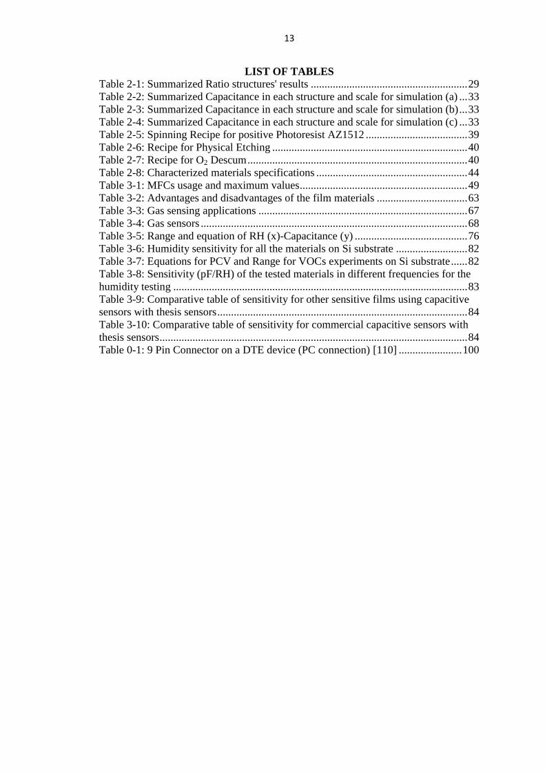
In general, the market size of sensors shows an expanding behavior that justifies
the growing research interest from companies and universities. As it can be easily
observed from the graph in Figure 1-1, the forecast is positive for the sensor market
with an anticipation of reaching approximately 11 USD billion in 2016 [6].
Figure 1-1: Worldwide sensor market and unit shipments from 2008 to 2016 [6]
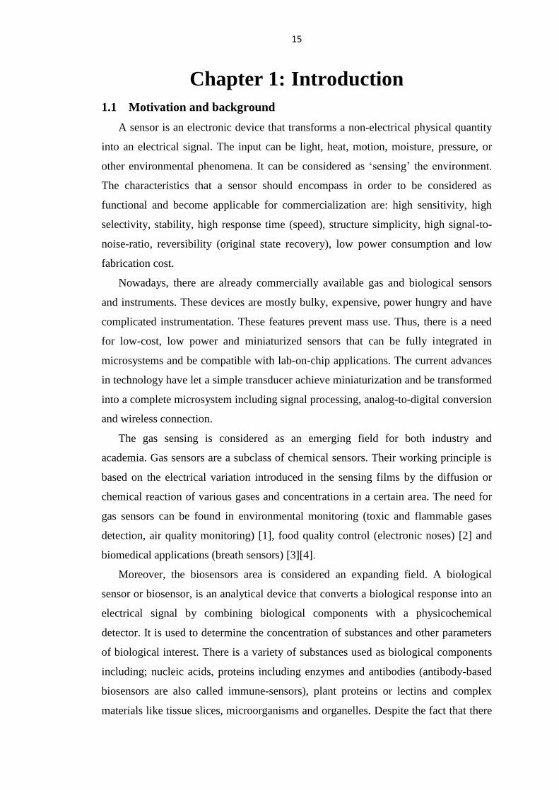
The gas sensors market follows the sensors market size behavior, which is the
overall available market. In Figure 1-2, the expanding market is shown with a forecast
in Figure 1-3 to reach the 2.5 billion by 2020. The most commonly used sensor types
are electrochemical, optical and piezoelectric. The main areas of demand are for
biomedical and safety precautions reasons in the developed markets of North America
and Europe. Moreover, there is demand for smart and wireless gas sensors for
enhancing the early detection of toxic gases in hazardous environmental conditions.
The new generation of cars using hydrogen will also increase the demand for this kind
of gas sensors.
17
Figure 1-2: Global gas sensor market estimate and forecast for 2010 – 2018 [7]
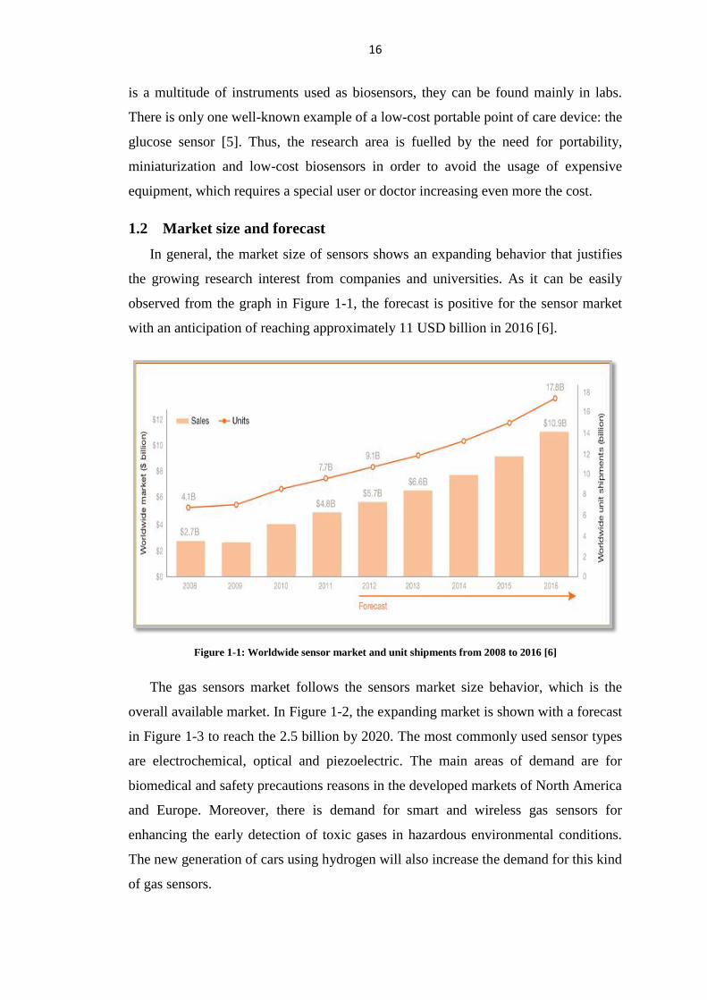
Figure 1-3: Global Gas sensors market by type in 2012 [8]
The most common sensors available in the market, as they can be observed in
Figure 1-3, are oxygen (O2), carbon monoxide (CO), carbon dioxide (CO2), nitrogen
oxides (NOx) and other sensors (methane (CH4), ammonia (NH3), hydrogen and
hydrocarbon sensors). Oxygen sensors are used in the automotive industry for
detecting the oxygen concentration in the vehicle’s exhaust and for equipping the
engine management system for controlling the fuel/air mix. Moreover, the NOx
sensors are used in the same section for monitoring the emissions from the vehicle in
order to meet regulatory compliances. Thus, the expansion of vehicle market can
affect these sensors' demand positively. For carbon dioxide sensors, there is demand
from the bulk food storage sector and industrial process for detecting spoilage.
18
Carbon monoxide sensors are used in industrial, food storage and packaging
applications.
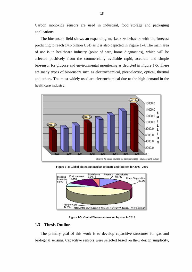
The biosensors field shows an expanding market size behavior with the forecast
predicting to reach 14.6 billion USD as it is also depicted in Figure 1-4. The main area
of use is in healthcare industry (point of care, home diagnostics), which will be
affected positively from the commercially available rapid, accurate and simple
biosensor for glucose and environmental monitoring as depicted in Figure 1-5. There
are many types of biosensors such as electrochemical, piezoelectric, optical, thermal
and others. The most widely used are electrochemical due to the high demand in the
healthcare industry.
Figure 1-4: Global biosensors market estimate and forecast for 2009 -2016
Figure 1-5: Global Biosensors market by area in 2016
1.3 Thesis Outline
The primary goal of this work is to develop capacitive structures for gas and
biological sensing. Capacitive sensors were selected based on their design simplicity,

19
low fabrication cost and the absence of DC power consumption. The contribution of
this thesis can be summarized in three points:
Chapter 2 includes the hand analysis, COMSOL Multiphysics simulations
and fabrication on Si and PET. It encompasses an investigation of the
dominant structure among interdigitated electrodes (IDEs), fractal curves
(Peano and Hilbert) and Archimedean spiral from capacitance density
perspective. Chapter 3 contains the humidity, volatile organic compounds (VOCs) and
Ammonia sensing of the Polyimide and Nafion polymers and Cu(bdc).xH2O
metal-organic framework (MOF) using IDEs. The automated gas setup that
was implemented and used for this part is extensively described in the
Appendix. Chapter 4 includes the biological sensing with experiments in CRP and BSA
quantification.

20
Chapter 2: Capacitive Sensors
In Chapter 2, a comparative study of different structures is conducted for
investigating the dominant structure in capacitance density. Additionally, a low cost
fabrication on PET for capacitive structures is described.
2.1 Concept of Capacitance
Capacitance can be defined as the electrical charge storage ability of an object.
The parallel plate capacitor, which is illustrated in Figure 2-1, is the most common
capacitor and its capacitance calculation is based on the formula (1):
𝐶 = 휀0휀𝑟𝐴
𝑑 (1)
The capacitance (𝐶) is based only on the geometric arrangement (𝐴 is the area of
the electrodes and 𝑑 is the distance between them) and the electric properties of any
non-conductors (휀𝑟 is the relative permittivity of dielectric film, 휀0 is the constant
relative permittivity of free space) in between the electrodes.
Figure 2-1: Parallel plate capacitor
Attempting to achieve lower dimensionality with keeping the capacitance at high
levels, the main challenge is to achieve a high capacitance density. PPC should be
mostly used as a model for calculating capacitance in the micro-level since it occupies
larger area. Due to downscaling, the lateral direction will assist in this direction since
the electrodes distance is inversely proportional to the capacitance. Moreover, in
microelectromechanical systems (MEMS) technology, the capacitance of this kind of
structure will be reduced since air will remain after the etching of the sacrificial layer.
Residual stresses will also lead to plate warping, showing that is an unreliable solution
for capacitance in micro scale. Finally, in order to avoid crosstalk effect between two
metal lines, the vertical spacing cannot follow the speed of shrinkage of the lateral
separation [10].
21
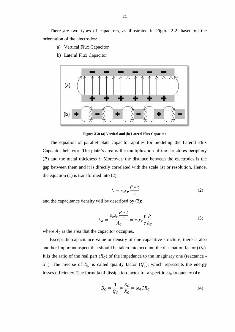
There are two types of capacitors, as illustrated in Figure 2-2, based on the
orientation of the electrodes:
a) Vertical Flux Capacitor
b) Lateral Flux Capacitor
Figure 2-2: (a) Vertical and (b) Lateral Flux Capacitor
The equation of parallel plate capacitor applies for modeling the Lateral Flux
Capacitor behavior. The plate’s area is the multiplication of the structures periphery
(𝑃) and the metal thickness 𝑡. Moreover, the distance between the electrodes is the
gap between them and it is directly correlated with the scale (𝑠) or resolution. Hence,
the equation (1) is transformed into (2):
𝐶 = 휀0휀𝑟𝑃 ∗ 𝑡
𝑠 (2)
and the capacitance density will be described by (3):
𝐶𝑑 =휀0휀𝑟
𝑃 ∗ 𝑡𝑠
𝐴𝐶= 휀0휀𝑟
𝑡
𝑠
𝑃
𝐴𝐶 (3)
where 𝐴𝐶 is the area that the capacitor occupies.
Except the capacitance value or density of one capacitive structure, there is also
another important aspect that should be taken into account, the dissipation factor (𝐷𝐶).
It is the ratio of the real part (𝑅𝐶) of the impedance to the imaginary one (reactance -
𝑋𝐶). The inverse of 𝐷𝐶 is called quality factor (𝑄𝐶), which represents the energy
losses efficiency. The formula of dissipation factor for a specific 𝜔0 frequency (4):
𝐷𝐶 =1
𝑄𝐶=𝑅𝐶𝑋𝐶= 𝜔0𝐶𝑅𝐶 (4)

22
The dissipation factor represents the ratio of the energy consumed based on
thermal losses over the stored one in an AC system. Thus, the dissipation factor
should be significantly low for the structure to have a pure reactance and not parasitic
resistance.
The quality factor does not have a constant value, it changes importantly by
frequency. This relies on two facts: the inverse proportional relationship of
capacitance with frequency and the difference of parasitic resistance due to skin
effect. Moreover, other attributes of the dielectric can be related to this change. A
desirable quality factor can be considered at the level of hundreds or thousands. The
level of the quality factor is based on the design of the capacitor and the quality of the
materials used.
2.2 Geometrical Formula Calculations
The main objective of this chapter is to find the dominant structure from the
capacitance density perspective. The 휀 = 휀0휀𝑟 is a constant value for this study since
no dielectric is used except air. The electrodes thickness 𝑡 is the same in all the
structures since the same process was followed. Thus, the only parameter that will
play an important role will be the ratio of the periphery to the area of the structure.
For this reason, structures that can maximize their periphery in a certain area have
been investigated from the geometrical perspective and then they were simulated and
fabricated.
The first step in this study is to investigate the geometrical characteristics of each
structure, the ratio of the periphery and the capacitor area. In this approach, the width
of the electrodes and the gap in between them are equal and are defined with a
parameter called scale (resolution). The structures under investigation are the
interdigitated electrodes (IDEs), the Archimedean spiral and the fractal curves, Hilbert
and Peano. The parameters used in the following calculations are: 𝑠: 𝑠𝑐𝑎𝑙𝑒,
𝐿: 𝐼𝐷𝐸𝑠 𝑙𝑒𝑛𝑔𝑡ℎ, 𝐶: 𝑐𝑜𝑟𝑛𝑒𝑟𝑠, 𝑃: 𝑝𝑒𝑟𝑖𝑝ℎ𝑒𝑟𝑦, 𝐴: 𝑎𝑟𝑒𝑎, 𝑅𝑎𝑡𝑖𝑜: 𝑅.
2.2.1 Interdigitated Electrodes (IDEs)
The most frequently used architecture is the interdigitated electrodes (IDEs),
which is depicted in Figure 2-3. This structure achieves high capacitance in
miniaturization, since its bars can be modeled as parallel plate capacitors in parallel,
which are separated by a distance 𝑔 and the plates area is the multiplication of finger

23
length 𝐿 and the metal thickness 𝑡. Except the sidewall capacitance between the
beams (fingers) that was before mentioned, there is also fringe capacitance (𝐶𝑓),
which appears on the edges of the fingers and is highly nonlinear. The summation of
both types provides the overall capacitance. The basic IDEs cell is depicted in
Figure 2-4, where are four corners. Especially in this structure, the effect of the
fringing field in the corners can be considered of not of such importance compared to
overall periphery, since the basic role it is played by the length of the finger.
Figure 2-3: 3D Interdigitated electrodes (IDEs)
Figure 2-4: IDE cell in 2d
The calculations for periphery (5), area (6) and ratio of them (7) of the basic IDEs
cell are the following:
𝑃𝐼𝐷𝐸𝑠 = 2(0.5𝑠 + 𝑐 + 𝐿 + 𝑐 + 0.5𝑠) = 2𝑠 + 2𝐿 + 4𝑐 (5)
𝐴𝐼𝐷𝐸𝑠 = 4𝑠 ∗ (𝐿 + 4𝑠) (6)
𝑅𝐼𝐷𝐸𝑠 = 2(𝑠 + 𝐿)
4𝑠(𝐿 + 4𝑠)=
𝑠 + 𝐿
2𝑠𝐿 + 8𝑠2=
𝑠𝐿 + 1
2𝑠 + 8𝑠2
𝐿
𝐿→∞⇒ 𝑅𝑎𝑡𝑖𝑜 =
1
2𝑠=0.5
𝑠 (7)
In the calculations for the IDEs ratio, the corners are not included and the length
of the finger is considered as infinite. This assumption is logical since normally the
length of the IDEs can be 20𝑠 or more. Thus, the path of the corners compared to the
overall is negligible.
24
2.2.2 Archimedean Spiral
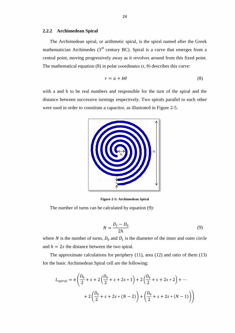
The Archimedean spiral, or arithmetic spiral, is the spiral named after the Greek
mathematician Archimedes (3rd
century BC). Spiral is a curve that emerges from a
central point, moving progressively away as it revolves around from this fixed point.
The mathematical equation (8) in polar coordinates (r, θ) describes this curve:
𝑟 = 𝑎 + 𝑏𝜃 (8)
with a and b to be real numbers and responsible for the turn of the spiral and the
distance between successive turnings respectively. Two spirals parallel to each other
were used in order to constitute a capacitor, as illustrated in Figure 2-5.
Figure 2-5: Archimedean Spiral
The number of turns can be calculated by equation (9):
𝛮 =𝐷1 − 𝐷02ℎ
(9)
where 𝛮 is the number of turns, 𝐷0 and 𝐷1 is the diameter of the inner and outer circle
and ℎ = 2𝑠 the distance between the two spiral.
The approximate calculations for periphery (11), area (12) and ratio of them (13)
for the basic Archimedean Spiral cell are the following:
𝐿𝑠𝑝𝑖𝑟𝑎𝑙 = 𝜋(𝐷02+ 𝑠 + 2 (
𝐷02+ 𝑠 + 2𝑠 ∗ 1) + 2 (
𝐷02+ 𝑠 + 2𝑠 ∗ 2) + ⋯
+ 2(𝐷02+ 𝑠 + 2𝑠 ∗ (𝑁 − 2)) + (
𝐷02+ 𝑠 + 2𝑠 ∗ (𝑁 − 1)))

25
𝐿𝑠𝑝𝑖𝑟𝑎𝑙 = 𝜋 (𝐷02+𝐷02+ 𝑠 + 2𝑠 ∗ (𝑁 − 1))
+ 2𝜋 ((𝐷02+ 𝑠 + 2𝑠 ∗ 1) + (
𝐷02+ 𝑠 + 2𝑠 ∗ 2) + ⋯
+ (𝐷02+ 𝑠 + 2𝑠 ∗ (𝑁 − 2)))
𝐿𝑠𝑝𝑖𝑟𝑎𝑙 = 𝜋(𝐷0 + 𝑠 + 2𝑠 ∗ (𝑁 − 1))
+ 2𝜋 ((𝑁 − 2)𝐷02+ (𝑁 − 2)𝑠 + 2𝑠(1 + 2 +⋯
+ (𝑁 − 2)))
(10)
From Gauss formula, the 𝑠𝑢𝑚(1,… ,𝑁 − 2) in (10) can be transformed into
(𝑁−2)(𝑁−1)
2 and, for our case, 𝐷0 = 10𝑠. Thus, the 𝐿𝑠𝑝𝑖𝑟𝑎𝑙 can be transformed into:
𝐿𝑠𝑝𝑖𝑟𝑎𝑙 = 𝜋(10𝑠 + 𝑠 + 2𝑠𝑁 − 2𝑠)
+ 2𝜋 ((𝑁 − 2)10𝑠
2+ (𝑁 − 2)𝑠 + 2𝑠
(𝑁 − 2)(𝑁 − 1)
2)
𝐿𝑠𝑝𝑖𝑟𝑎𝑙 = 𝜋(9𝑠 + 2𝑠𝑁) + 2𝜋(6𝑠(𝑁 − 2) + 𝑠(𝑁 − 2)(𝑁 − 1))
𝐿𝑠𝑝𝑖𝑟𝑎𝑙 = 𝜋(9𝑠 + 2𝑠𝑁) + 2𝜋𝑠(𝑁 − 2)(𝑁 + 5)
𝐿𝑠𝑝𝑖𝑟𝑎𝑙 = 𝜋𝑠(9𝑠 + 2𝑁 + 2𝑁2 + 6𝑁 − 20) = 𝜋𝑠(2𝑁2 + 8𝑁 − 11) (11)
{512𝑠 → 2 ∗ 62 𝑤 → 𝑁
→ 𝑁
𝑤=0.24
𝑠→ 𝑤 =
𝑁
0.24𝑠
𝐴𝑠𝑝𝑖𝑟𝑎𝑙 = 𝑤2 = (
𝑁
0.24𝑠)2
(12)
𝑅𝑠𝑝𝑖𝑟𝑎𝑙 = 𝜋𝑠(2𝑁2 + 8𝑁 − 11)
(𝑁0.24 𝑠)
2 =(0.24)2𝜋𝑠(2𝑁2 + 8𝑁 − 11)
𝑁2 ∗ 𝑠2𝑠
𝑅𝑠𝑝𝑖𝑟𝑎𝑙 =0.180864
𝑠(2 + 8/𝑁 − 11/𝑁2)
𝑁→∞⇒ 𝑅𝑠𝑝𝑖𝑟𝑎𝑙 =
0.3617
𝑠 (13)
2.2.3 Fractal Capacitors
Fractal structures were selected in the concept of searching for high periphery.
They are repeating patterns being based on mathematical models. The basic

26
geometrical difference of the fractals compared to the other figures is based on the
order. In general, if the total length or of the radius of a rectangle or a sphere
respectively is doubled, the area will be increased four times (22) and the volume
eight times (23). For the fractals, if the same occurs, the power will not be guaranteed
that it will be an integer. This power is named fractal dimension, usually exceeding
the fractal's topological dimension [11]. The primary challenge was based on the high
periphery, which could increase in a proportional way the capacitance based on the
PPC model. Based on this characteristic, the selected fractal models were the Peano’s
and Hilbert’s curve.
2.2.3.1 Peano Curve
The Peano curve was invented and named after Giuseppe Peano in 1890. It was
the first example of a space-filling curve. The process of creating higher orders is
described in Figure 2-6. It can be simply explained as the following:
i. There are nine equal squares (Figure 2-6a), which centers are connected as
it is shown in Figure 2-6b in order to constitute the generator for this
curve.
ii. Then, the generator is included in each of the new 9 squares in order to
create the 1st Peano order (Figure 2-6c). The generator cells should be
symmetrical, in x-axis and y-axis for the up-down and the right-left
adjacent squares structures respectively.
iii. This process is repeated every time for achieving a higher order.
Figure 2-6: Creation of Peano’s curve higher orders
In the fabrication process, it is common that the straight 90o corner cannot be
achieved without some curvity in the edge. Thus, a variation of the Normal Peano

27
Curve (Figure 2-7), named Curvature Peano Curve (Figure 2-8), is employed for
adding curvity around the edges of the electrodes. Moreover, for the Normal Peano
Curve, there are a large number of corners, which should be taken into account.
The calculations for periphery (14)(15), area (16), corners (17) and ratio (18)(19)
of both basic cells of normal and curvature Peano curve are the following:
𝑃𝑃𝑒𝑎𝑛𝑜 = 4𝑠 ∗ (5 + 2 + 4 + 2 + 5) = 4 ∗ 18𝑠 = 72𝑠 (14)
𝑃𝑃𝑒𝑎𝑛𝑜 𝐶𝑢𝑟𝑣𝑎𝑡𝑢𝑟𝑒 = 4𝑠(4 + 𝜋 + 2 + 𝜋 + 4) = 4𝑠(10 + 2𝜋)
= 65.1327𝑠 (15)
𝐴𝑃𝑒𝑎𝑛𝑜 = 12𝑠 ∗ 12𝑠 = 144𝑠2 (16)
𝐶𝑃𝑒𝑎𝑛𝑜 = 𝑠 ∗ 4 ∗ 4 = 16𝑠 (17)
𝑅𝑃𝑒𝑎𝑛𝑜 =
56𝑠
144𝑠2+ (
16𝑠
144𝑠2)𝐶= 0.3889
𝑠+ (0.1111
𝑠)𝐶 (18)
𝑅𝑃𝑒𝑎𝑛𝑜 𝐶𝑢𝑟𝑣𝑎𝑡𝑢𝑟𝑒 =
65.1327𝑠
144𝑠2= 0.4523/𝑠 (19)
The effect of the corners in the capacitance cannot be calculated with simple
equations since it is highly non-linear. It will be tried to be approached in the
simulations. For the hand calculations, the curvature results will be considered close
to the real one.
2.2.3.2 Hilbert Curve
David Hilbert, a German mathematician, invented a continuous fractal space-
filling curve in 1891, which was a variant of Peano curves. The concept of Hilbert
Figure 2-7: Normal Peano Curve Cell
Figure 2-8: Curvature Peano Curve Cell

28
curve is illustrated in Figure 2-9 and it is similar to Peano curve creation. The main
difference is that the basic squares are four in this case and in the previous were nine.
Thus, the construction of N Hilbert order in 2D, 22 copies should be placed in an N-1
2D Hilbert curve in each corner, rotate them and connect them by line segments as it
is shown in Figure 2-9c and Figure 2-9d for the 1st and 2
nd order respectively.
Figure 2-9: Creation of Hilbert’s curve higher orders
In the Hilbert Curve (Figure 2-10), the same variation of curvature (Figure 2-11)
as for Peano curve has been applied.
Figure 2-10: Normal Hilbert Cell
Figure 2-11: Curvature Hilbert Cell
Moreover, in the Normal Hilbert Curve [12], the corners play a vital role for the
overall capacitance, since they occur more times compared to Peano in a specific area
and thus they should be taken into careful consideration. The calculations for
periphery (20)(21), area (22), corners (23) and ratio (24)(25) of both basic cells of
normal and curvature Peano curve are the following:

29
𝑃𝐻𝑖𝑙𝑏𝑒𝑟𝑡 = 2𝑠 ∗ (3 + 2 + 2 + 4 + 2 + 2 + 1) = 32𝑠 (20)
𝑃𝐻𝑖𝑙𝑏𝑒𝑟𝑡 𝐶𝑢𝑟𝑣𝑎𝑡𝑢𝑟𝑒 = 2𝑠 ∗ (2 + 𝜋 + 𝜋/2 + 2 + 𝜋 + 𝜋/2)
= 2𝑠(4 + 3𝜋) = 26.85𝑠 (21)
𝐴𝐻𝑖𝑙𝑏𝑒𝑟𝑡 = 8𝑠 ∗ 8𝑠 = 64𝑠2 (22)
𝐶𝐻𝑖𝑙𝑏𝑒𝑟𝑡 = 𝑠 ∗ 3 ∗ 4 = 12𝑠 (23)
𝑅𝐻𝑖𝑙𝑏𝑒𝑟𝑡 =
20𝑠
64𝑠2+ (
12𝑠
64𝑠2)𝐶= 0.3125
𝑠+ (0.1875
𝑠)𝐶 (24)
𝑅𝐻𝑖𝑙𝑏𝑒𝑟𝑡 𝐶𝑢𝑟𝑣𝑎𝑡𝑢𝑟𝑒 =
26.85𝑠
64𝑠2= 0.4195/𝑠 (25)
As it can be observed from the comparative Table 2-1 and Figure 2-12, IDEs
dominate in the ratio compared to the other structures. Peano, Hilbert and Spiral
follow in that order from the ratio perspective, which is directly proportional to the
capacitance density. In the Figure 2-12, the curvature Hilbert and Peano curves are
used, since are considered to be closer to the fabrication results and the corners cannot
be quantified with simple calculations.
Table 2-1: Summarized Ratio structures' results
Structure w/o Corners Curvature w/ Corners
IDEs 0.5/𝑠 𝟎. 𝟓/𝒔 0.5/𝑠 Peano 0.3889/𝑠 𝟎. 𝟒𝟓𝟐𝟑/𝒔 0.5/𝑠
Hilbert 0.3125/𝑠 𝟎. 𝟒𝟏𝟗𝟓/𝒔 0.5/𝑠 Spiral 0.3617/𝑠 𝟎. 𝟑𝟔𝟏𝟕/𝒔 0.3617/𝑠
Figure 2-12: Ratio vs scale diagram
0
0.1
0.2
0.3
0.4
0.5
1 2 3 4 5
Rat
io
Scale
IDEs Peano
Hilbert Spiral

30
2.3 Simulations
Finite element simulations using COMSOL Multiphysics were carried out for the
capacitive structures (Interdigitated electrodes (IDEs), Peano curve electrodes, Hilbert
curve electrodes, Archimedean Spiral electrodes). The main scope was to determine
the dominant structure from the capacitance density perspective.
For the capacitance calculation, the 3D Electrostatics physics in the AC/DC
Module was employed. The model is defined by the domain equations and the
boundary conditions.
(a) Domain equations
The charge, 𝑄, and the electric scalar potential, 𝑉, are connected via Poisson’s
equation (26):
–𝛻 ⋅ (휀0휀𝑟𝛻𝑉) = 𝜌 (26)
where 휀0 is the permittivity of free space, 휀𝑟 is the relative permittivity and 𝜌 is the
space charge density (𝜌 ∝ 𝑄). The electric field and the displacement are obtained
from the gradient of 𝑉:
𝐸 = – 𝛻𝑉
D = 휀0휀𝑟𝐸 (27)
(b) Boundary conditions
Potential boundary conditions are applied to the capacitor plates and bars. The 𝛥𝑉
between the two electrodes is 1 V. The one electrode’s potential is fixed at 1 V and
the other is grounded. For the surface of the surrounding box, zero surface charge at
the boundary is applied:
𝑛 ⋅ 𝐷 = 0 (28)
The capacitance can be calculated from:
𝐶 = 𝑄
𝑉
The structures were designed in L-edit and were inserted in the COMSOL
Multiphysics as DXF files. The size of the structure was parametrized providing the
opportunity for parametric sweep in the scale. A Silicon substrate of 20𝑠 um and a
SiO2 layer of 2 um have been used. For the electrodes, gold has been utilized with a
thickness of 350 nm. The electrodes thickness affects the capacitance since any
change in them can have an effect on the area of the electrodes.
31
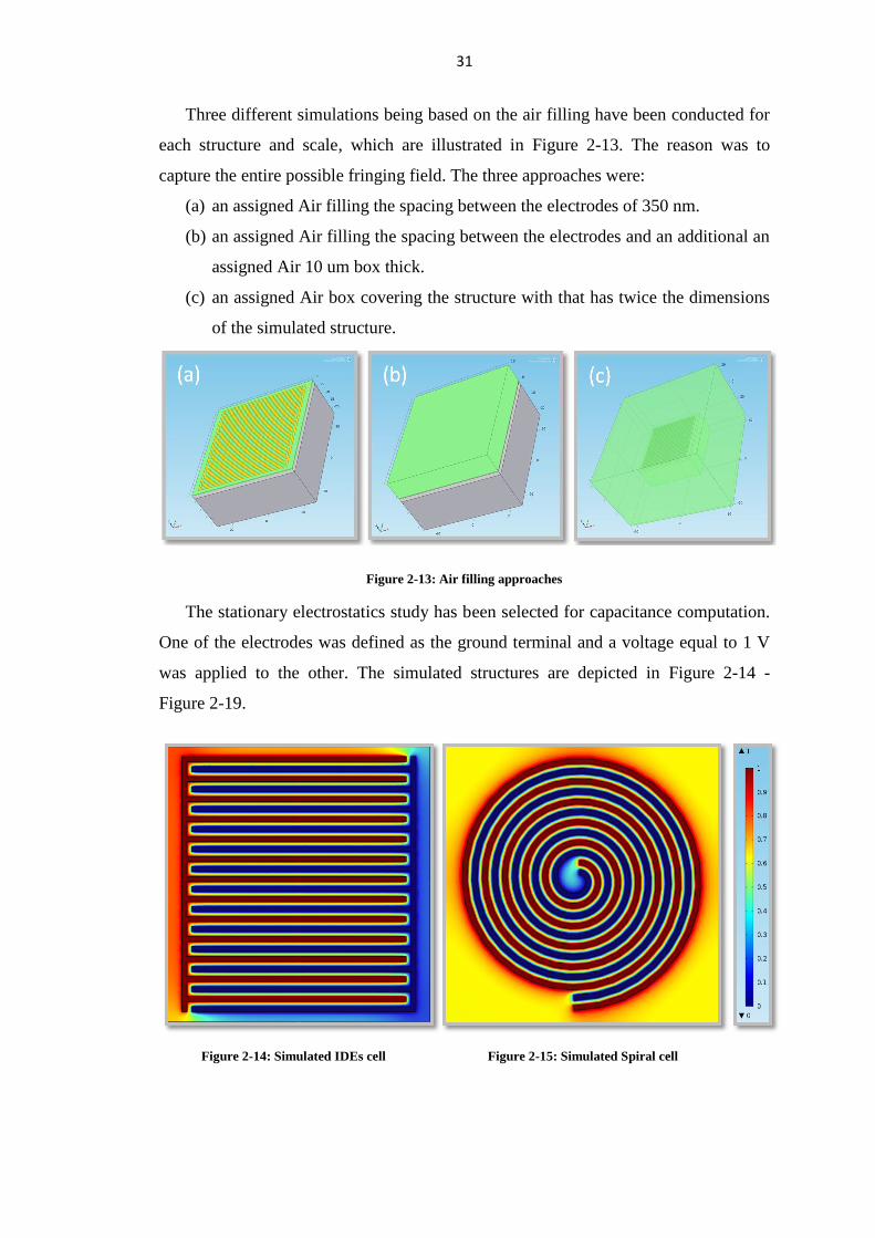
Three different simulations being based on the air filling have been conducted for
each structure and scale, which are illustrated in Figure 2-13. The reason was to
capture the entire possible fringing field. The three approaches were:
(a) an assigned Air filling the spacing between the electrodes of 350 nm.
(b) an assigned Air filling the spacing between the electrodes and an additional an
assigned Air 10 um box thick.
(c) an assigned Air box covering the structure with that has twice the dimensions
of the simulated structure.
Figure 2-13: Air filling approaches
The stationary electrostatics study has been selected for capacitance computation.
One of the electrodes was defined as the ground terminal and a voltage equal to 1 V
was applied to the other. The simulated structures are depicted in Figure 2-14 -
Figure 2-19.
Figure 2-14: Simulated IDEs cell
Figure 2-15: Simulated Spiral cell

32
Figure 2-16: Simulated Peano N cell
Figure 2-17: Simulated Peano C cell
Figure 2-18: Simulated Hilbert N cell
Figure 2-19: Simulated Hilbert C cell
In the simulations, the scale was swept from 1 um to 5 um. In Figure 2-20 and
Table 2-4, the capacitance vs scale diagram shows the dominance of IDEs obviously
for the simulation (c). Then, the ratio of capacitance value to the area that the
capacitor occupies, the decrease in capacitance density with the increase of scale is
depicted in Figure 2-21. Those results have a direct connection with the corner effect.
Thus, since the IDEs are not facing this issue in the extent that fractals do, it achieves
higher capacitance density. The electrical field in corners is not uniform and as dense
as in the straight paths. This is also the reason that the Peano curve achieves higher
capacitance than Hilbert curve since there are fewer corners in the first structure.
Finally, the spiral curve is achieving the lowest value since the effective area is less
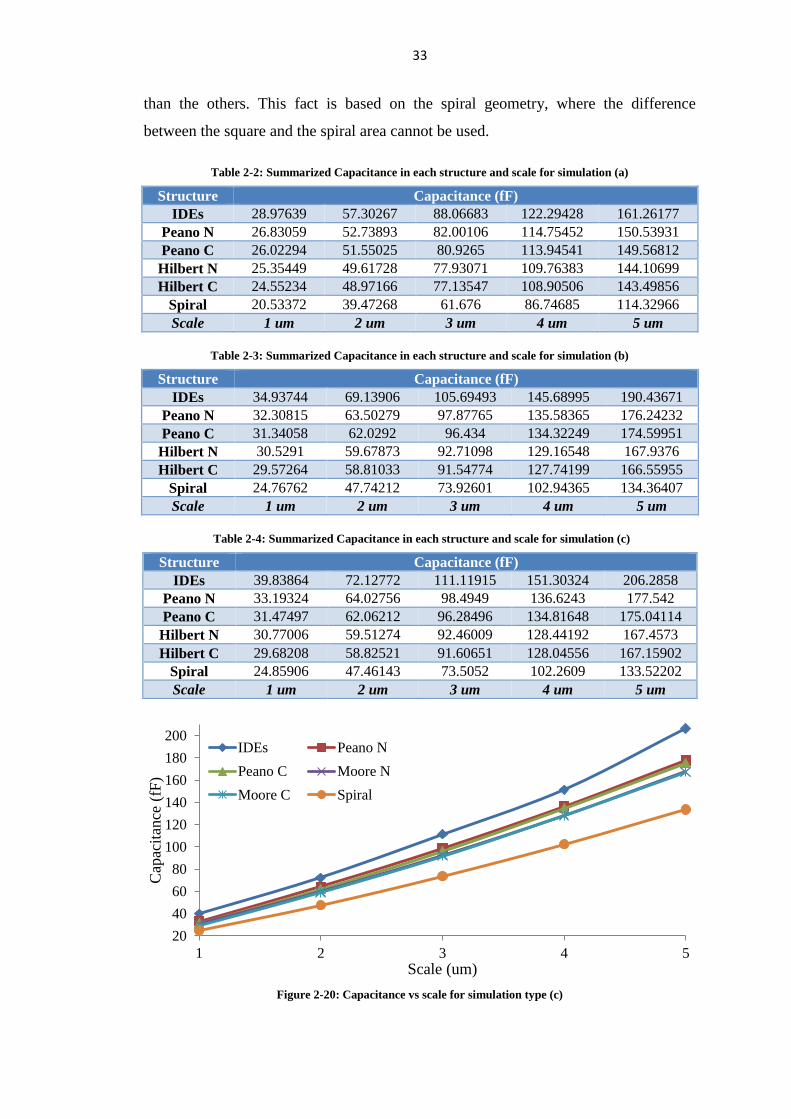
33
than the others. This fact is based on the spiral geometry, where the difference
between the square and the spiral area cannot be used.
Table 2-2: Summarized Capacitance in each structure and scale for simulation (a)
Structure Capacitance (fF)
IDEs 28.97639 57.30267 88.06683 122.29428 161.26177
Peano N 26.83059 52.73893 82.00106 114.75452 150.53931
Peano C 26.02294 51.55025 80.9265 113.94541 149.56812
Hilbert N 25.35449 49.61728 77.93071 109.76383 144.10699
Hilbert C 24.55234 48.97166 77.13547 108.90506 143.49856
Spiral 20.53372 39.47268 61.676 86.74685 114.32966
Scale 1 um 2 um 3 um 4 um 5 um
Table 2-3: Summarized Capacitance in each structure and scale for simulation (b)
Structure Capacitance (fF)
IDEs 34.93744 69.13906 105.69493 145.68995 190.43671
Peano N 32.30815 63.50279 97.87765 135.58365 176.24232
Peano C 31.34058 62.0292 96.434 134.32249 174.59951
Hilbert N 30.5291 59.67873 92.71098 129.16548 167.9376
Hilbert C 29.57264 58.81033 91.54774 127.74199 166.55955
Spiral 24.76762 47.74212 73.92601 102.94365 134.36407
Scale 1 um 2 um 3 um 4 um 5 um
Table 2-4: Summarized Capacitance in each structure and scale for simulation (c)
Structure Capacitance (fF)
IDEs 39.83864 72.12772 111.11915 151.30324 206.2858
Peano N 33.19324 64.02756 98.4949 136.6243 177.542
Peano C 31.47497 62.06212 96.28496 134.81648 175.04114
Hilbert N 30.77006 59.51274 92.46009 128.44192 167.4573
Hilbert C 29.68208 58.82521 91.60651 128.04556 167.15902
Spiral 24.85906 47.46143 73.5052 102.2609 133.52202
Scale 1 um 2 um 3 um 4 um 5 um
Figure 2-20: Capacitance vs scale for simulation type (c)
20
40
60
80
100
120
140
160
180
200
1 2 3 4 5
Cap
acit
ance
(fF
)
Scale (um)
IDEs Peano N
Peano C Moore N
Moore C Spiral
34
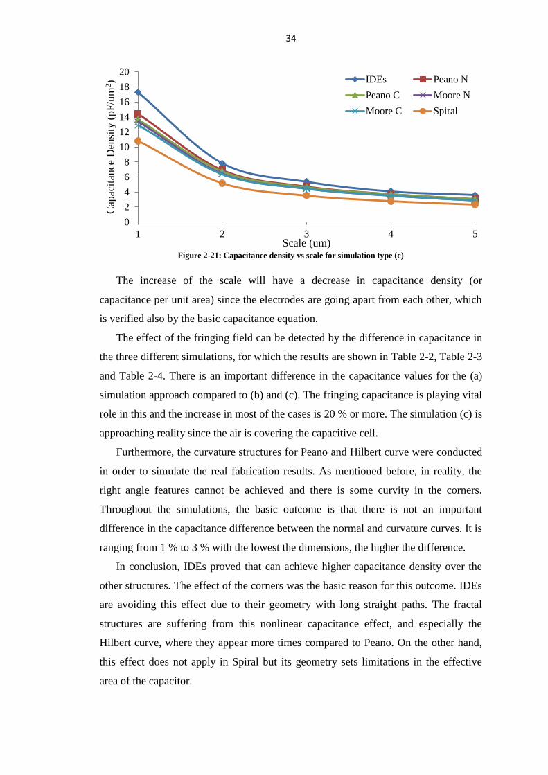
Figure 2-21: Capacitance density vs scale for simulation type (c)
The increase of the scale will have a decrease in capacitance density (or
capacitance per unit area) since the electrodes are going apart from each other, which
is verified also by the basic capacitance equation.
The effect of the fringing field can be detected by the difference in capacitance in
the three different simulations, for which the results are shown in Table 2-2, Table 2-3
and Table 2-4. There is an important difference in the capacitance values for the (a)
simulation approach compared to (b) and (c). The fringing capacitance is playing vital
role in this and the increase in most of the cases is 20 % or more. The simulation (c) is
approaching reality since the air is covering the capacitive cell.
Furthermore, the curvature structures for Peano and Hilbert curve were conducted
in order to simulate the real fabrication results. As mentioned before, in reality, the
right angle features cannot be achieved and there is some curvity in the corners.
Throughout the simulations, the basic outcome is that there is not an important
difference in the capacitance difference between the normal and curvature curves. It is
ranging from 1 % to 3 % with the lowest the dimensions, the higher the difference.
In conclusion, IDEs proved that can achieve higher capacitance density over the
other structures. The effect of the corners was the basic reason for this outcome. IDEs
are avoiding this effect due to their geometry with long straight paths. The fractal
structures are suffering from this nonlinear capacitance effect, and especially the
Hilbert curve, where they appear more times compared to Peano. On the other hand,
this effect does not apply in Spiral but its geometry sets limitations in the effective
area of the capacitor.
0
2
4
6
8
10
12
14
16
18
20
1 2 3 4 5
Cap
acit
ance
Den
sity
(pF
/um
2)
Scale (um)
IDEs Peano N
Peano C Moore N
Moore C Spiral
35
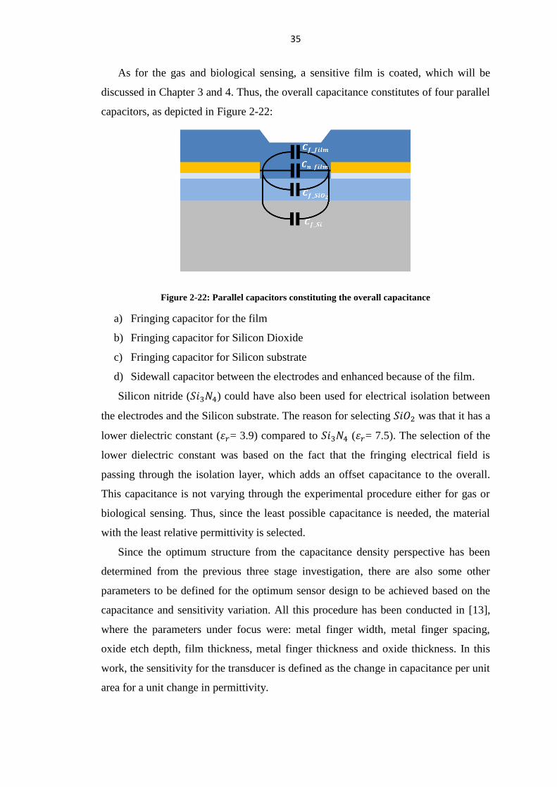
As for the gas and biological sensing, a sensitive film is coated, which will be
discussed in Chapter 3 and 4. Thus, the overall capacitance constitutes of four parallel
capacitors, as depicted in Figure 2-22:
Figure 2-22: Parallel capacitors constituting the overall capacitance
a) Fringing capacitor for the film
b) Fringing capacitor for Silicon Dioxide
c) Fringing capacitor for Silicon substrate
d) Sidewall capacitor between the electrodes and enhanced because of the film.
Silicon nitride (𝑆𝑖3𝑁4) could have also been used for electrical isolation between
the electrodes and the Silicon substrate. The reason for selecting 𝑆𝑖𝑂2 was that it has a
lower dielectric constant (휀𝑟= 3.9) compared to 𝑆𝑖3𝑁4 (휀𝑟= 7.5). The selection of the
lower dielectric constant was based on the fact that the fringing electrical field is
passing through the isolation layer, which adds an offset capacitance to the overall.
This capacitance is not varying through the experimental procedure either for gas or
biological sensing. Thus, since the least possible capacitance is needed, the material
with the least relative permittivity is selected.
Since the optimum structure from the capacitance density perspective has been
determined from the previous three stage investigation, there are also some other
parameters to be defined for the optimum sensor design to be achieved based on the
capacitance and sensitivity variation. All this procedure has been conducted in [13],
where the parameters under focus were: metal finger width, metal finger spacing,
oxide etch depth, film thickness, metal finger thickness and oxide thickness. In this
work, the sensitivity for the transducer is defined as the change in capacitance per unit
area for a unit change in permittivity.
36
The thickness of the metal can affect the sensitivity. The sidewall field
capacitance will be increased, since the electrodes surface will be increased. The
increase of the finger spacing (gap) will decrease the capacitance since it is inverse
proportional to it. The effect of metal finger width cannot be defined directly from the
capacitance formula. The increase of the finger width will increase the fringing field
but the sidewall field will not change. The increase in the electrodes width will also
affect the area occupied by the electrodes and thus this can affect in the opposite way
the capacitance density. Due to this opposite effect, no more interest will be given in
this parameter and it will be set equal to the electrodes gap. Moreover, the increase of
finger width and/or gap will affect the capacitance change, which will be less linear
since the sidewall capacitance will play less important role compared to the fringing.
Another parameter that can affect the sensitivity is the sensing film thickness. The
outcome of this study has shown there is an increase in the sensitivity, when the
sensing film thickness increases. This is based on the enhancement of the fringing
field, which passes through the film. This increase saturates when the sensing film
thickness is equal to the summation of the finger width and gap, which happens
regardless of the individual values of Wm and Sm. Thus, the film should be selected
to be close to that value if the absorption is the mechanism that affects the relative
permittivity. If the film is thicker, this can affect the sensor dynamics as the diffusion
time is proportional to square of the diffusion distance [14], in addition to decreasing
the change in permittivity.
The sensitivity can also be increased by over etching the oxide in the gap between
the electrodes, since the fringing field can pass through there and enhanced because of
the presence of the sensitive film. This fact requires conformal deposition of the
sensitive film. It should be noted that in order the oxide etch will have a positive
impact on the sensitivity if the sensing film thickness is greater compared to the
summation of metal thickness and oxide etch thickness. This is important in order to
fill the electrodes gap, which volume has been increased by the oxide over etching.
2.4 Cleanroom fabrication
L-Edit software from Tanner was used to draw the layout of capacitive structures.
The sketches are depicted in the previous section. All the cell dices in the design were
square areas. The square cell width was 512𝑠 and it is illustrated in Figure 2-23. Due
to the limitations of the mask writing and lithography tools available in KAUST
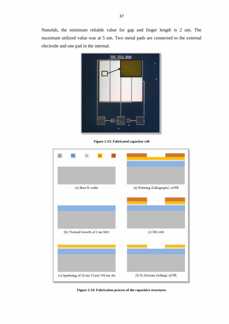
37
Nanofab, the minimum reliable value for gap and finger length is 2 um. The
maximum utilized value was at 5 um. Two metal pads are connected to the external
electrode and one pad in the internal.
Figure 2-23: Fabricated capacitor cell
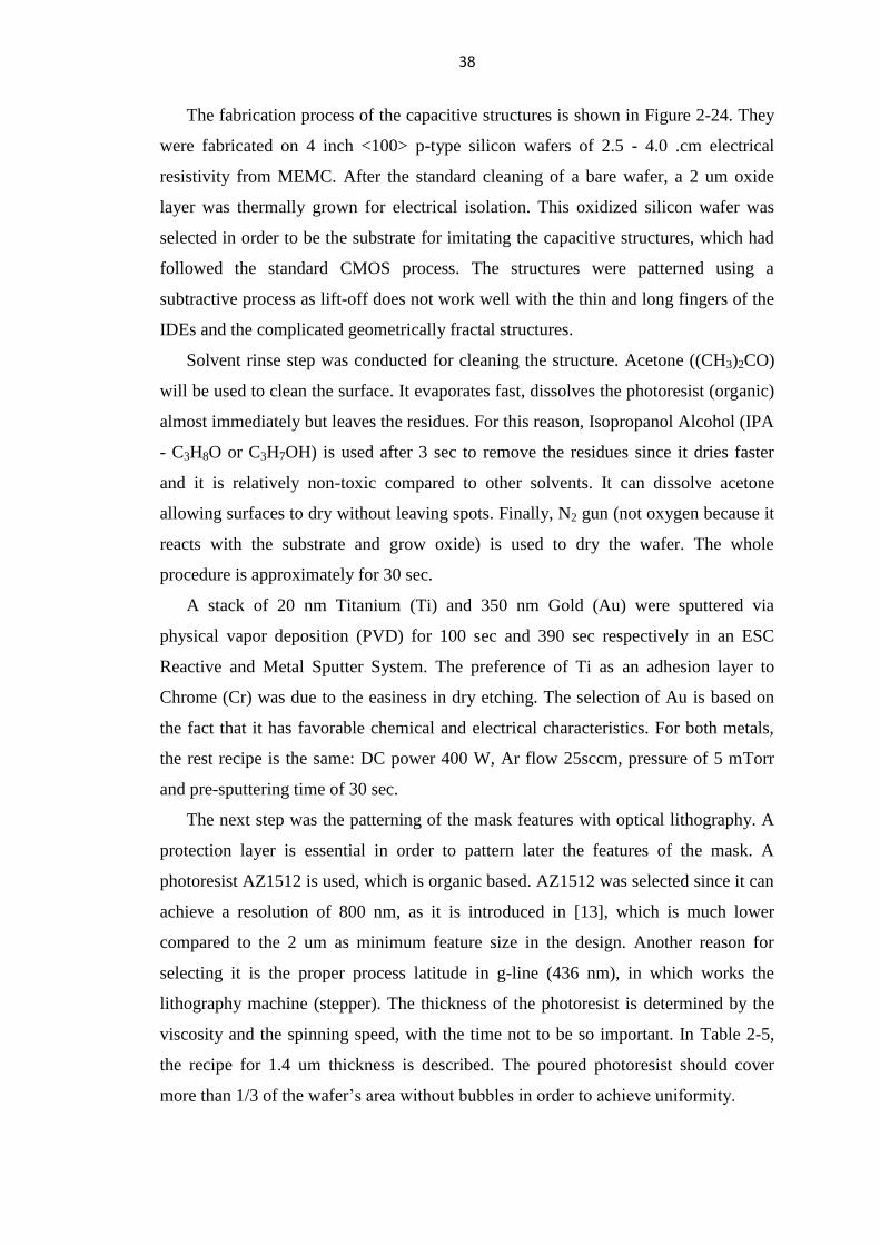
Figure 2-24: Fabrication process of the capacitive structures
38
The fabrication process of the capacitive structures is shown in Figure 2-24. They
were fabricated on 4 inch <100> p-type silicon wafers of 2.5 - 4.0 .cm electrical
resistivity from MEMC. After the standard cleaning of a bare wafer, a 2 um oxide
layer was thermally grown for electrical isolation. This oxidized silicon wafer was
selected in order to be the substrate for imitating the capacitive structures, which had
followed the standard CMOS process. The structures were patterned using a
subtractive process as lift-off does not work well with the thin and long fingers of the
IDEs and the complicated geometrically fractal structures.
Solvent rinse step was conducted for cleaning the structure. Acetone ((CH3)2CO)
will be used to clean the surface. It evaporates fast, dissolves the photoresist (organic)
almost immediately but leaves the residues. For this reason, Isopropanol Alcohol (IPA
- C3H8O or C3H7OH) is used after 3 sec to remove the residues since it dries faster
and it is relatively non-toxic compared to other solvents. It can dissolve acetone
allowing surfaces to dry without leaving spots. Finally, N2 gun (not oxygen because it
reacts with the substrate and grow oxide) is used to dry the wafer. The whole
procedure is approximately for 30 sec.
A stack of 20 nm Titanium (Ti) and 350 nm Gold (Au) were sputtered via
physical vapor deposition (PVD) for 100 sec and 390 sec respectively in an ESC
Reactive and Metal Sputter System. The preference of Ti as an adhesion layer to
Chrome (Cr) was due to the easiness in dry etching. The selection of Au is based on
the fact that it has favorable chemical and electrical characteristics. For both metals,
the rest recipe is the same: DC power 400 W, Ar flow 25sccm, pressure of 5 mTorr
and pre-sputtering time of 30 sec.
The next step was the patterning of the mask features with optical lithography. A
protection layer is essential in order to pattern later the features of the mask. A
photoresist AZ1512 is used, which is organic based. AZ1512 was selected since it can
achieve a resolution of 800 nm, as it is introduced in [13], which is much lower
compared to the 2 um as minimum feature size in the design. Another reason for
selecting it is the proper process latitude in g-line (436 nm), in which works the
lithography machine (stepper). The thickness of the photoresist is determined by the
viscosity and the spinning speed, with the time not to be so important. In Table 2-5,
the recipe for 1.4 um thickness is described. The poured photoresist should cover
more than 1/3 of the wafer’s area without bubbles in order to achieve uniformity.

39
Table 2-5: Spinning Recipe for positive Photoresist AZ1512
Step Speed (rpm) Ramp (rpm/s) Time (sec)
1st 800 1000 3
2nd
1500 1500 3
3rd
3000 3000 30
The spinning process followed by a soft baking at 100 oC for 60 sec. This step was
made to remove the solvents, increase the adhesion of the photoresist and solidify it.
The photoresist should not be exposed to a higher temperature or stay in the bake for
more than the suggested time, which for this kind of photoresist is at 90 to 100 oC for
30 to 60 sec [13]. Otherwise, the photoresist will be made too hard and difficult to be
dissolved later.
A 5-inch bright field optical mask was created using Heidelberg uPG101 Laser
Mask Writer. Optical exposure was used to transfer the pattern from the mask to the
photoresist with using a stepper. It contains a UV light lamp of 20mW, which exposes
the open areas and transfers the areal image (mask pattern) to a latent image (3D in
the resist). The selected recipe was based on the used photoresist, with inserting 1.4
um for the thickness and selecting 40 mJ/cm2
as exposure energy.
The next step was to develop the soluble parts of the photoresist. The wafer was
immersed in 726 MIF Developer in a culture dish for 35 sec (strictly timed by an
alarm) and then it was submerged in a beaker with DI H2O to stop the reaction and
then washed in the basin. Finally, for dehydrating, N2 was used. The bowl was
cleaned and the used developer was removed by using a vacuum gun (aspirator) for
safety. The time of development varies on the type of the photoresist and its thickness.
The suggested time for developing this specific photoresist is 40 sec [13]. So, the
selected time acts as a precaution for avoiding damaging the unexposed areas and
causing harm to the structures’ shapes. The MIF developers are used in CMOS
processes because the fact that they are free of metal ions will not allow them to
create salts on our devices.
The metal layer was patterned by dry etching using Oxford Instruments
PlasmaLab System. The recipe for physical etching is described in Table 2-6. The RF
power value is relatively high. This recipe achieves approximately an etching rate of
50nm/min for Au and 60nm/min for Ti.
40
Table 2-6: Recipe for Physical Etching
RF power ICP power Table Temp. Pressure Time Ar
125 W 1000 W 10 oC 10 mTorr 7.5 min 30 sccm
Since the acetone could not strip the photoresist layer completely due to the dry
etching step, thus the O2 descum was used. In general, it is used to strip the
photoresist, when it is useless. It is removed by a plasma containing oxygen, which
oxidizes it. This process is called ‘ashing’ and resembles dry etching. Another way to
achieve the photoresist removal is by chemically alternating it so that it no longer
adheres to the substrate by a liquid ‘resist stripper’. For the effective photoresist strip,
the recipe described in Table 2-7 was followed. The RF power value is relatively low.
Higher values are not selected in order to protect the features.
Table 2-7: Recipe for O2 Descum
RF power ICP power Table Temp. Pressure Time O2
30 W 1500 W 50 oC 50 mTorr 2 min 50 sccm
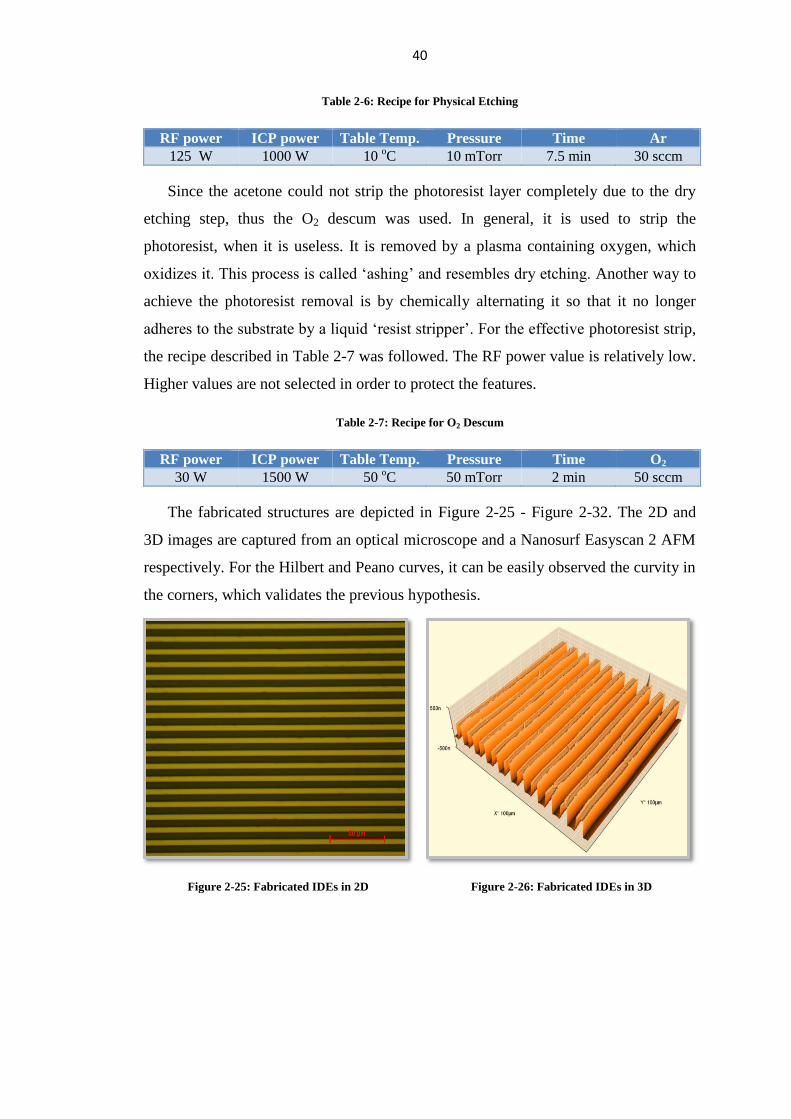
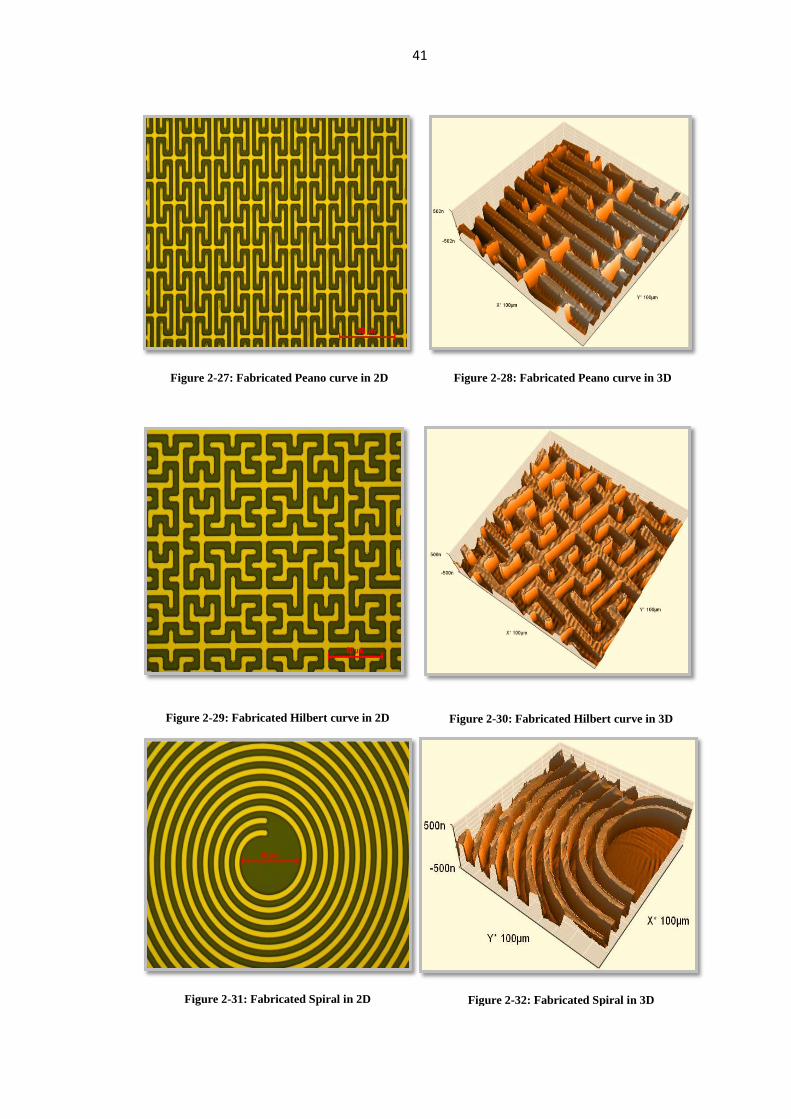
The fabricated structures are depicted in Figure 2-25 - Figure 2-32. The 2D and
3D images are captured from an optical microscope and a Nanosurf Easyscan 2 AFM
respectively. For the Hilbert and Peano curves, it can be easily observed the curvity in
the corners, which validates the previous hypothesis.
Figure 2-25: Fabricated IDEs in 2D
Figure 2-26: Fabricated IDEs in 3D
41
Figure 2-27: Fabricated Peano curve in 2D
Figure 2-28: Fabricated Peano curve in 3D
Figure 2-29: Fabricated Hilbert curve in 2D
Figure 2-30: Fabricated Hilbert curve in 3D
Figure 2-31: Fabricated Spiral in 2D
Figure 2-32: Fabricated Spiral in 3D
42
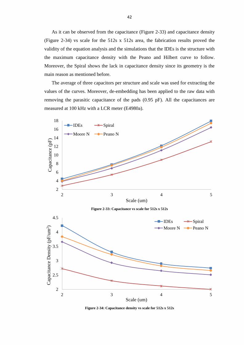
As it can be observed from the capacitance (Figure 2-33) and capacitance density
(Figure 2-34) vs scale for the 512s x 512s area, the fabrication results proved the
validity of the equation analysis and the simulations that the IDEs is the structure with
the maximum capacitance density with the Peano and Hilbert curve to follow.
Moreover, the Spiral shows the lack in capacitance density since its geometry is the
main reason as mentioned before.
The average of three capacitors per structure and scale was used for extracting the
values of the curves. Moreover, de-embedding has been applied to the raw data with
removing the parasitic capacitance of the pads (0.95 pF). All the capacitances are
measured at 100 kHz with a LCR meter (E4980a).
Figure 2-33: Capacitance vs scale for 512s x 512s
Figure 2-34: Capacitance density vs scale for 512s x 512s
2
4
6
8
10
12
14
16
18
2 3 4 5
Cap
acit
ance
(pF
)
Scale (um)
IDEs Spiral
Moore N Peano N
2
2.5
3
3.5
4
4.5
2 3 4 5
Cap
acit
ance
Den
sity
(pF
/um
2)
Scale (um)
IDEs Spiral
Moore N Peano N

43
2.5 Low-cost fabrication on PET substrate
2.5.1 Flexible Materials Characterization
The high cost of cleanroom processes and Si substrates has led this work to focus
also on reducing the cost and simplifying the fabrication of our sensor. PET was
preferred for its flexibility, low-cost and its adhesion ability with Au, which is
important since metal peel off is an issue faced in flexible substrates. Moreover, the
use of use of paper, plastic and fabric substrates has attracted the interest due to their
flexibility and stretchability. These types of materials were selected to be
characterized based on their relative permittivity and loss tangent (tanθ), which are the
most indicative characteristics of a material.
Permittivity describes the relation of the material with the electric field. More
specifically, it is the measure of resistance that an electric field faces in order to be
formed: the lower the permittivity of a material, the higher the electric flux. The
dielectric loss, which is parameterized through the loss tangent, is the measure of
electromagnetic energy dissipation into heat. The complex relative permittivity is
explained in the equation 29:
휀𝑟∗ =
휀∗
휀0= 휀𝑟
′ − 𝑗휀𝑟′′ = (
휀′
휀0) − 𝑗 (
휀′′
휀0) (29)
As it can be observed from Equation 29, the dielectric constant is a complex
number. The real (εr′ ) and imaginary (εr
′′) part are of the measures of stored energy
and material’s dissipation to an external field respectively. The loss tangent is
calculated by the equation 30:
𝑡𝑎𝑛𝛿 =휀𝑟′′
휀𝑟′ (30)
The real and imaginary parts have a phase of 90o. Their summation provides the
complex permittivity and its difference in angle with the real part gives the loss angle.
For the material characterization the Agilent E4991A Impedance analyzer was
utilized. It follows the measurement method of parallel plate. The utilized method for
measuring the permittivity is the contacting parallel electrode plate. There are two
electrodes, one fixed and one adjustable based on the thickness of the device under
test (DUT), which are squeezing the material. The instrument measures the
capacitance and the dissipation factor of this capacitor, from which the 휀𝑟∗ and 𝑡𝑎𝑛𝛿
are calculated respectively.
44
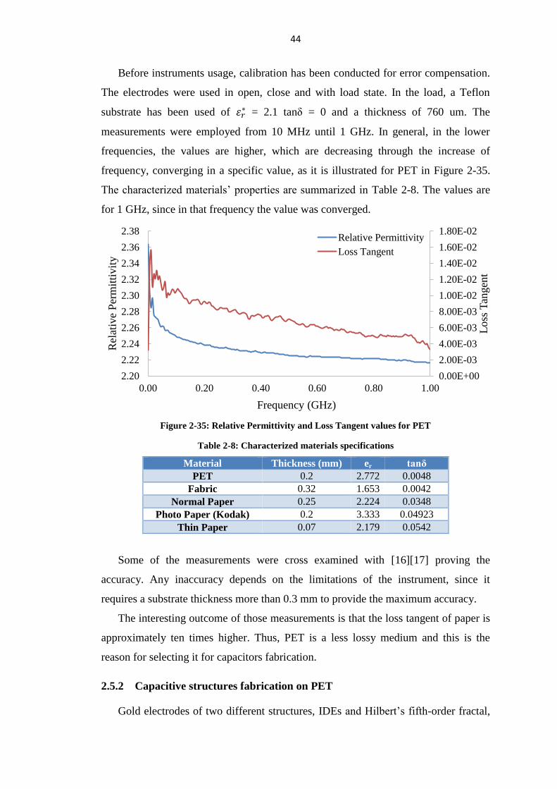
Before instruments usage, calibration has been conducted for error compensation.
The electrodes were used in open, close and with load state. In the load, a Teflon
substrate has been used of 휀𝑟∗ = 2.1 tanδ = 0 and a thickness of 760 um. The
measurements were employed from 10 MHz until 1 GHz. In general, in the lower
frequencies, the values are higher, which are decreasing through the increase of
frequency, converging in a specific value, as it is illustrated for PET in Figure 2-35.
The characterized materials’ properties are summarized in Table 2-8. The values are
for 1 GHz, since in that frequency the value was converged.
Figure 2-35: Relative Permittivity and Loss Tangent values for PET
Table 2-8: Characterized materials specifications
Material Thickness (mm) er tanδ
PET 0.2 2.772 0.0048
Fabric 0.32 1.653 0.0042
Normal Paper 0.25 2.224 0.0348
Photo Paper (Kodak) 0.2 3.333 0.04923
Thin Paper 0.07 2.179 0.0542
Some of the measurements were cross examined with [16][17] proving the
accuracy. Any inaccuracy depends on the limitations of the instrument, since it
requires a substrate thickness more than 0.3 mm to provide the maximum accuracy.
The interesting outcome of those measurements is that the loss tangent of paper is
approximately ten times higher. Thus, PET is a less lossy medium and this is the
reason for selecting it for capacitors fabrication.
2.5.2 Capacitive structures fabrication on PET
Gold electrodes of two different structures, IDEs and Hilbert’s fifth-order fractal,
0.00E+00
2.00E-03
4.00E-03
6.00E-03
8.00E-03
1.00E-02
1.20E-02
1.40E-02
1.60E-02
1.80E-02
2.20
2.22
2.24
2.26
2.28
2.30
2.32
2.34
2.36
2.38
0.00 0.20 0.40 0.60 0.80 1.00
Loss
Tan
gen
t
Rel
ativ
e P
erm
itti
vit
y
Frequency (GHz)
Relative Permittivity
Loss Tangent
45
have been utilized. It is proposed a low-cost and simple process for fabricating
flexible sensors. Sputtering Au was preferred to ink-jet printing silver
electrodes [18][19] since metal, due to its purity, achieves a lower dissipation factor
compared to conductive ink. Moreover, our capacitive sensors have no DC power
consumption compared to [20], where microheaters are needed. IDEs are commonly
used, but in this work, the Hilbert's fractal structure was also investigated due to its
potential for higher capacitance density. The curvature of the corners smoothens out
any possible electric field peak.
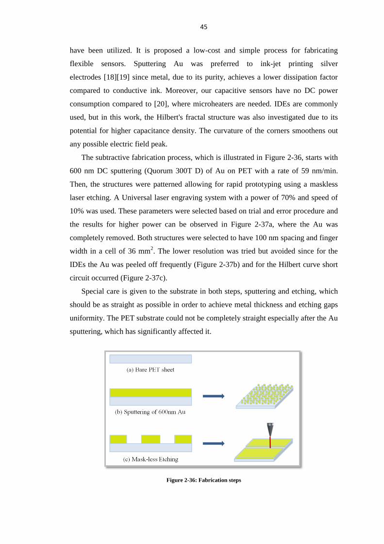
The subtractive fabrication process, which is illustrated in Figure 2-36, starts with
600 nm DC sputtering (Quorum 300T D) of Au on PET with a rate of 59 nm/min.
Then, the structures were patterned allowing for rapid prototyping using a maskless
laser etching. A Universal laser engraving system with a power of 70% and speed of
10% was used. These parameters were selected based on trial and error procedure and
the results for higher power can be observed in Figure 2-37a, where the Au was
completely removed. Both structures were selected to have 100 nm spacing and finger
width in a cell of 36 mm2. The lower resolution was tried but avoided since for the
IDEs the Au was peeled off frequently (Figure 2-37b) and for the Hilbert curve short
circuit occurred (Figure 2-37c).
Special care is given to the substrate in both steps, sputtering and etching, which
should be as straight as possible in order to achieve metal thickness and etching gaps
uniformity. The PET substrate could not be completely straight especially after the Au
sputtering, which has significantly affected it.
Figure 2-36: Fabrication steps
46
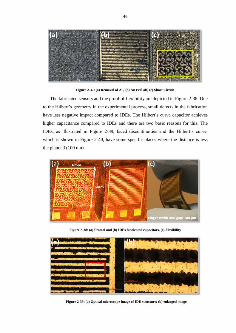
Figure 2-37: (a) Removal of Au, (b) Au Peel off, (c) Short Circuit
The fabricated sensors and the proof of flexibility are depicted in Figure 2-38. Due
to the Hilbert’s geometry in the experimental process, small defects in the fabrication
have less negative impact compared to IDEs. The Hilbert’s curve capacitor achieves
higher capacitance compared to IDEs and there are two basic reasons for this. The
IDEs, as illustrated in Figure 2-39, faced discontinuities and the Hilbert’s curve,
which is shown in Figure 2-40, have some specific places where the distance is less
the planned (100 um).
Figure 2-38: (a) Fractal and (b) IDEs fabricated capacitors, (c) Flexibility
Figure 2-39: (a) Optical microscope image of IDE structure; (b) enlarged image.

47
Figure 2-40: (a) Optical microscope image of Hilbert structure; (b) enlarged image.
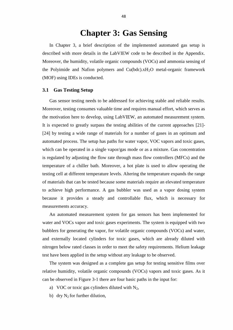
48
Chapter 3: Gas Sensing
In Chapter 3, a brief description of the implemented automated gas setup is
described with more details in the LabVIEW code to be described in the Appendix.
Moreover, the humidity, volatile organic compounds (VOCs) and ammonia sensing of
the Polyimide and Nafion polymers and Cu(bdc).xH2O metal-organic framework
(MOF) using IDEs is conducted.
3.1 Gas Testing Setup
Gas sensor testing needs to be addressed for achieving stable and reliable results.
Moreover, testing consumes valuable time and requires manual effort, which serves as
the motivation here to develop, using LabVIEW, an automated measurement system.
It is expected to greatly surpass the testing abilities of the current approaches [21]-
[24] by testing a wide range of materials for a number of gases in an optimum and
automated process. The setup has paths for water vapor, VOC vapors and toxic gases,
which can be operated in a single vapor/gas mode or as a mixture. Gas concentration
is regulated by adjusting the flow rate through mass flow controllers (MFCs) and the
temperature of a chiller bath. Moreover, a hot plate is used to allow operating the
testing cell at different temperature levels. Altering the temperature expands the range
of materials that can be tested because some materials require an elevated temperature
to achieve high performance. A gas bubbler was used as a vapor dosing system
because it provides a steady and controllable flux, which is necessary for
measurements accuracy.
An automated measurement system for gas sensors has been implemented for
water and VOCs vapor and toxic gases experiments. The system is equipped with two
bubblers for generating the vapor, for volatile organic compounds (VOCs) and water,
and externally located cylinders for toxic gases, which are already diluted with
nitrogen below rated classes in order to meet the safety requirements. Helium leakage
test have been applied in the setup without any leakage to be observed.
The system was designed as a complete gas setup for testing sensitive films over
relative humidity, volatile organic compounds (VOCs) vapors and toxic gases. As it
can be observed in Figure 3-1 there are four basic paths in the input for:
a) VOC or toxic gas cylinders diluted with N2,
b) dry N2 for further dilution,
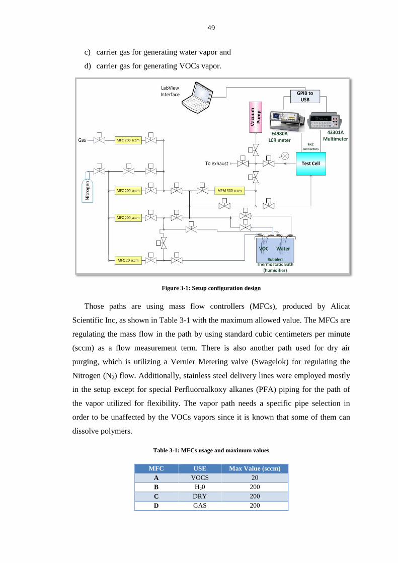
49
c) carrier gas for generating water vapor and
d) carrier gas for generating VOCs vapor.
Figure 3-1: Setup configuration design
Those paths are using mass flow controllers (MFCs), produced by Alicat
Scientific Inc, as shown in Table 3-1 with the maximum allowed value. The MFCs are
regulating the mass flow in the path by using standard cubic centimeters per minute
(sccm) as a flow measurement term. There is also another path used for dry air
purging, which is utilizing a Vernier Metering valve (Swagelok) for regulating the
Nitrogen (N2) flow. Additionally, stainless steel delivery lines were employed mostly
in the setup except for special Perfluoroalkoxy alkanes (PFA) piping for the path of
the vapor utilized for flexibility. The vapor path needs a specific pipe selection in
order to be unaffected by the VOCs vapors since it is known that some of them can
dissolve polymers.
Table 3-1: MFCs usage and maximum values
MFC USE Max Value (sccm)
A VOCS 20
B H20 200
C DRY 200
D GAS 200
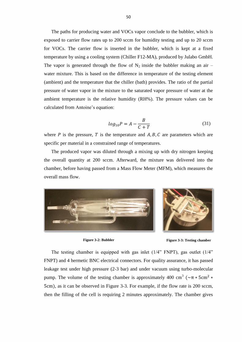
50
The paths for producing water and VOCs vapor conclude to the bubbler, which is
exposed to carrier flow rates up to 200 sccm for humidity testing and up to 20 sccm
for VOCs. The carrier flow is inserted in the bubbler, which is kept at a fixed
temperature by using a cooling system (Chiller F12-MA), produced by Julabo GmbH.
The vapor is generated through the flow of N2 inside the bubbler making an air –
water mixture. This is based on the difference in temperature of the testing element
(ambient) and the temperature that the chiller (bath) provides. The ratio of the partial
pressure of water vapor in the mixture to the saturated vapor pressure of water at the
ambient temperature is the relative humidity (RH%). The pressure values can be
calculated from Antoine’s equation:
𝑙𝑜𝑔10𝑃 = 𝐴 −𝐵
𝐶 + 𝑇 (31)
where 𝑃 is the pressure, 𝑇 is the temperature and 𝐴, 𝐵, 𝐶 are parameters which are
specific per material in a constrained range of temperatures.
The produced vapor was diluted through a mixing up with dry nitrogen keeping
the overall quantity at 200 sccm. Afterward, the mixture was delivered into the
chamber, before having passed from a Mass Flow Meter (MFM), which measures the
overall mass flow.
Figure 3-2: Bubbler
Figure 3-3: Testing chamber
The testing chamber is equipped with gas inlet (1/4” FNPT), gas outlet (1/4”
FNPT) and 4 hermetic BNC electrical connectors. For quality assurance, it has passed
leakage test under high pressure (2-3 bar) and under vacuum using turbo-molecular
pump. The volume of the testing chamber is approximately 400 cm3 (~π ∗ 5cm2 ∗
5cm), as it can be observed in Figure 3-3. For example, if the flow rate is 200 sccm,
then the filling of the cell is requiring 2 minutes approximately. The chamber gives

51
the ability to the user to measure two sensors with BNC connectors and arrays of
sensors by using a D15 connector.
Especially for the humidity testing, the chamber encompasses two sensors; a
commercial humidity sensor (HIH-4000-003) and the implemented capacitive sensor
using IDEs. The commercial one can give the actual humidity level inside the
chamber, which allows to detect the difference in capacitance for the implemented at
different humidity levels. The output voltage of the commercial sensor is read by a
Multimeter (Agilent 43301A) and it is fed by the DC source of the LCR meter
(Agilent E4980A), which also measures the capacitance of the testing sensors. The
outlet of the chamber concludes to the exhaust or it is absorbed by a vacuum pump
(Mastercool Inc.).
Regarding humidity testing, condensation is an important issue that should be
considered and avoided. If the bath temperature reaches the ambient, then the relative
humidity will reach 100% and condensation occurs. Condensation is the physical
process where a material changes its physical state from gas to liquid. This
phenomenon can also be defined as the change of the water vapor into liquid water
when it is attached to a surface. It contaminates the system and needs special
treatment to avoid it. Heating the pipes at an elevated temperature for a long period of
time can be one practical solution, in order to let the liquid evaporate.
Concluding, as it can be observed in Figure 3-4, the testing setup consists of the:
(A) Nitrogen (N2) cylinder.
(B) main setup, which consists of the four MFC’s (explained in Table 3-1), one MFM,
stainless steel pipes and taps to control the flow of the gas and Multi-drop
Breakout Box (BB9 Series), in which all the MFC’s are connected for power and
data transfer to laptop.
(C) cooling system – chiller (Julabo), which keeps the temperature of the bubbler in
specific temperature.
(D) bubbler, which generates the vapor.
(E) chamber, inside which there are two sensors. The one is commercial sensor, which
can give as output the humidity inside the chamber. The other is the implemented
capacitive sensor (using materials with different permittivity per time) by the
Sensors Lab, which changes its capacitance during the changes of the humidity in
the chamber.
(F) hot plate, which allows the chamber to work at elevated temperatures.
52
(G) LCR meter for measuring the capacitance of the implemented under test sensor.
(H) Multimeter, for measuring the output voltage of the commercial humidity sensor.
(I) Laptop remotely controlled, for avoiding the presence in the experiment time.
Figure 3-4: Implemented testing setup
3.1.1 LabVIEW Automation
The automation of the testing setup was achieved by using National Instruments
(NI) LabVIEW. LabVIEW is computer software with a graphical programming
language. The graphical programming language helps in creating fast prototypes.
National Instruments has many applications that have compatibility with LabVIEW
and many libraries are already implemented to assist in coding. LabVIEW assists in
acquiring data and controlling devices via different communication protocols and
cables (e.g. NI GPIB (IEEE 488), RS232 to USB). The main file is called vi and the
files that are included and used in the main subvis.
For the purposes of our setup, two main vis were implemented for data
acquisition with curves extraction using LCR meter and Multimeter and experiment
automation with control of MFCs, chiller and hot plate, as it can be observed in
Figure 3-5 and Figure 3-6 respectively. All instruments are designed to run either

53
independently or not from each other depending on the usage that the user wants to
have. A more detailed description of the instruments and LabVIEW code can be
found in the Appendix.
Figure 3-5: Front Panel of data acquisition with curves extraction
Figure 3-6: Front Panel of Experiment automation
3.2 Sensitive film materials
The classification of the sensors can be conducted based on the sensing material
used. The materials under investigation will be separated into four categories: Metal
54
Oxide Semiconductors (MOS), Carbon Nanomaterials, Metal-Organic Frameworks
(MOFs) and Polymers. In general, the parameters that can affect the sensors’
sensitivity are the operating temperature and environmental humidity.
3.2.1 Metal Oxide Semiconductors (MOS)
MOS are used as a sensing material for gas detection by varying their electric
conductivity when a compatible gas reacts with it. This kind of sensors is also called
as chemiresistor. There are two main classes, which are separated based on oxidation
states: non-transition (one oxidation state - e.g. Al2O3) and transition (more oxidation
states – e.g. Fe2O3). Of course, since the number of oxidation states is increased, the
consumed energy is also increased. For the transition type, there are electronic
configurations of d0 (e.g., TiO2, V2O5, WO3) and d
10 (e.g., SnO2 and ZnO). The n-type
is the dominant type of MOS for gas sensing films but also there are some p-type
material (NiOx), with their basic difference to be the operating temperature which is
lower for p-type [1].
The process for detecting gases by using MOS has two phases. Firstly, there are
redox reactions, where O− is spread in the film area will react with the target gas’s
molecules. Secondly, this change can be sensed by transforming the electronic
resistance of the sensor. This change is commonly detected by measuring the
impedance. For example, for detecting VOCs, the absorbed O2 is reacting with them,
reducing the effect of trapped electrons. This has an impact on the resistance, which is
dependent on the reaction on the semiconductor and the metal oxide [4].
There are some examples in the literature on which MOS films react with specific
gases. One example is Tin dioxide (SnO2), which electronic resistance is changing by
exposing in variation of gas concentration of liquefied petroleum gas (LPG), methane
(CH4), carbon monoxide (CO). Moreover, tungsten trioxide (WO3) is known for
compatibility with hydrogen (H2) and nitrogen oxide (NO) [1]. Furthermore, the
response of different structures of ZnO to acetone was explored in [25] using a
temperature range from 200 to 450 oC reaching a value of 95% for specific structure.
The response of ZnO to H2S and NO gases was examined [26], with the H2S response
to increase in grain and intra-grain boundary resistance and NO’s to arise only in
grain boundary resistance. Moreover, there is also a comparative study of sensors
using TiO2 and ZnO, which has been activated by UV light and are working at room
temperature. It was proven that the response values of TiO2 to ethanol and
55
formaldehyde gases were much larger than those of ZnO, which shows that TiO2 is a
potential material for photo-activated gas sensors [27].
One notable application for measuring acetone from human breath is explored
in [28]. This study takes advantage of the fact that the acetone concentration differs
for healthy people (300 to 900 ppb) and diabetics (>1800 ppb). An indication of high
acetone will increase the possibility of having diabetes. They developed a portable
chemo-resistive sensor and applied to real breath acetone detection. The sensor was
heated in the back of the substrate and the film was based on Si-doped WO3
nanoparticles.
Another approach with using tungsten oxide (WO3) is mentioned in [29] for
monitoring NO in the direction of providing information for health signature in
breath. The microelectronic chip consists of a Sapphire substrate. In the center of it in
the top layer, there are the Platinum IDEs and WO3 film of 50 nm. In the bottom
layer, there is a miniature hot plate helping the chip to operate at an elevated
temperature at 300 to 500°C. The heater burns gases on the sensor surface and the
electrodes will assist in monitoring a change in the film’s materials properties
indicating the presence of a specific target gas.
Furthermore, there are cases where a specific treatment should be applied to the
sensing material for achieving higher sensitivity. For instance, SnO2 needs to be
preheated in order to achieve higher ability for molecule adsorption. This can be an
obstacle for real applications since an important drift in the optimal operation
temperature can decrease the sensitivity remarkably and causing poor selectivity.
Moreover, there are also occasions that the same material can have different operating
temperatures for different gases, e.g. SnO2 for CH4 (400 °C) and CO (90 °C). This
seems to be an obstacle that can be overcome by using a multi-heated sensor arrays.
Concluding, working at elevated temperatures increases the power dissipation, the
cost and the complexity of the system which has led to solutions as micro-heaters,
reducing all of them remarkably. Another problem to be faced is the recovery time
that is long in some cases. This is an important obstacle to create sensing platforms,
where the gas concentrations change rapidly.
3.2.2 Carbon nanomaterials
Carbon nanomaterials are investigated the last years for their unique electrical,
optical and mechanical properties. Those attributes have paved the way for the
56
development of miniaturized and low-power sensors. Common carbon nanomaterials
utilized for gas sensing are nanotubes (CNTs), nanofibers (CNFs) and graphene.
3.2.2.1 Carbon nanotubes (CNTs)
CNTs are allotropes of carbon with a cylindrical nanostructure. Their main
attribute that distinguishes them from the other materials is length-to-diameter ratio,
which has reached 132,000,000:1 [30]. They can be fabricated by using conventional
methods as lithography and their mechanical properties allow them to be compatible
with flexible devices [31].
They can operate at room temperature and they have high sensitivity in gases as
alcohol, ammonia (NH3), carbon dioxide (CO2) and nitrogen oxide (NOx). Their
nature to operate in ambient temperature releases the need for using heaters and paves
the way for achieving low-power and low-weight devices. CNTs structure allows a
great adsorptive capacity and high response time that can have an effect on their
electric properties as capacitance and resistance [32].
There are two main classes for the CNTs: single-walled carbon nanotubes
(SWCNTs) and multiwall carbon nanotubes (MWCNTs). SWCNTs have been used
for sensing of toxic gases and MWCNTs for carbon dioxide (CO2), oxygen (O2) and
ammonia (NH3). Of course, the selectivity and the response time differentiate from
one gas to another. Moreover, it is a common practice to use other materials with
CNTs in order to increase their sensitivity and selectivity. Another use of them is to
detect sulfur hexafluoride (SF6), which can increase the CNTs’ electrical conductance.
Moreover, as for CNFs, CNTs can be decorated with Pt, Pd, Au, Rh, Sn, Mg, Fe,
Co, Ni, Zn, Mo, W, V and Cr and used in an array for detecting carbon monoxide
(CO), nitrogen dioxide (NO2), methane (CH4), hydrogen sulphide (H2S), ammonia
(NH3) and hydrogen (H2), as it was attempted in [33].
Another important breakthrough on development gas sensors based on CNTs was
achieved in [34]. It can operate at varying humidity levels, which can lead to
commercialization. SWNT layers were utilized and coated with seven polycyclic
aromatic hydrocarbons (PAH) compounds by drop-casting. Different combinations of
PAH/SWNT sensors were exposed to volatile organic compounds, in which humidity
level was varying from 5–80% RH, achieving high sensitivity and accuracy values.
This achievement has paved the way for detecting VOCs in real applications.
57
3.2.2.2 Carbon nanofibers (CNFs)
CNFs are cylindrical nanostructures with graphene layers arranged as stacked
cones, cups or plates. Carbon nanofibers with graphene layers wrapped into perfect
cylinders are called carbon nanotubes. The main characteristics of CNFs are
discontinuous, highly graphitic and highly compatible with most polymer processing
techniques. Their unique surface state assists on functionalization and other
alternation methods for the surface in order the nanofibers to the host polymer.
CNFs, in which polystyrene was added under magnetic stirring, have been used
for detecting toluene. Moreover, it has been employed to use carbon nanofibers with
metal oxide for detecting dimethyl methylphosphonate (DMMP) by performing
standard resistive measurements at room temperature. Another approach has used
Polypyrrole (PPy)-coated carbon nanofibers, which has been fabricated by using one-
step vapor deposition polymerization (VDP). It has been used as a toxic gas sensor for
ammonium (NH3) and hydrochloric acid (HCl) detection [35].
CNFs were also used as decoration for WO3 with single-nozzle co-electrospinning
method. This film was exposed to NO2, but the recovery time was high in room
temperature [36]. For this reason UV light illumination used to face this problem
effectively. The sensitivity was increased when the concentration of WO3 was
increased since the CNFs could absorb more NO2 gas.
Moreover, CNFs were decorated with metal nanoparticles (Au, Pd) in IDEs [20],
which were ink-jet printed using silver ink on a flexible polyimide substrate. It was
exposed in ammonium (NH3) and nitrogen dioxide (NO2). The response to the gases
depends on the metal decoration with Au and Pd, in which the responses were
different. For example, Pd increases the response to NH3 while Au diminishes it.
Thus, the selectivity of CNFs can be enhanced adding specific elements.
3.2.2.3 Graphene
Graphene is pure carbon in the form of a very thin, nearly transparent sheet, which
consists of a two-dimensional array of carbon atoms covalently connected by sp2
bonds. The first lab production achieved in 2004 [37]. Graphene has become one of
the most common used materials for its exceptionally high crystal and electronic
quality. Gas sensors seem to be one of the areas that graphene is employed based on
its advantageous properties. The two-dimensional array let all the graphene atoms to

58
be exposed and it has high surface area per unit volume. Moreover, it is highly
conductive with the crystal defects to be few.
The graphene’s inventors has tried to use it in gas sensing applications [38]. It has
been observed that the resistivity differs with different magnitudes for various gases.
It can also be indicated by the sign of the change if the gas was an electron acceptor
(e.g., nitrogen dioxide, moisture) or an electron donor (e.g., carbon monoxide, ethanol
and ammonia).
Another approach has focused on doping graphene for enhancing the
sensitivity [39]. It was proven that B or S doped graphene had the ability to detect
NOx. It was also used to detect NO2 and it was tested under air and NO2 gas ambients
showing reproducibility for ambient alternation [40].
The synthesizing of SnO2 nanorods on graphene sheets was suggested in [41].
They achieved highly aligned structures in 3-D array by a straightforward crystal-
seeds-directing hydrothermal method. By varying the seeding concentration and
temperature, the diameter and density of the SnO2 nanorods growth on the graphene
sheets was tuned. It has shown a remarkable improvement (over twice sometimes) in
the response of the sensor on many gases as Hydrogen sulfide (H2S), Formaldehyde
(HCHO), Ethanol (C2H5OH). This effect is based on the large surface area of SnO2
nanorod arrays and the magnificent electronic characteristics of graphene.
3.2.3 Metal-Organic Frameworks (MOFs)
Metal-organic frameworks (MOFs) are a class of crystalline materials whose
crystal structure is made up of metal-containing clusters connected by multidentate
organic linkers. MOFs are a class of hybrid materials. They are considered as
promising materials for gas sensing because of their extraordinarily large surface
areas, high porosity and structural variety [1]. They are stable up until or above 200
oC [42]. The sorption capacity of the MOF will determine the maximum observable
signal [43].
The pore size or shape of the MOFs is not the only way for efficient capture of
unsafe gases or vapors. Available open metal sites with no saturated center or
modifications on the pore surface are possible ways to enhance selectivity and
efficiency of the sensing film interacting with the desirable gas or vapor via
coordination bonds, acid–base/electrostatic interactions, p-complex/H-bonding
formation, etc [1][42][44].
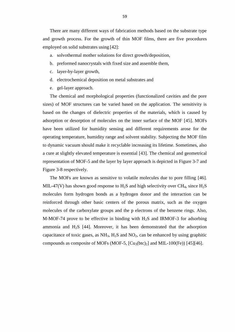
59
There are many different ways of fabrication methods based on the substrate type
and growth process. For the growth of thin MOF films, there are five procedures
employed on solid substrates using [42]:
a. solvothermal mother solutions for direct growth/deposition,
b. preformed nanocrystals with fixed size and assemble them,
c. layer-by-layer growth,
d. electrochemical deposition on metal substrates and
e. gel-layer approach.
The chemical and morphological properties (functionalized cavities and the pore
sizes) of MOF structures can be varied based on the application. The sensitivity is
based on the changes of dielectric properties of the materials, which is caused by
adsorption or desorption of molecules on the inner surface of the MOF [45]. MOFs
have been utilized for humidity sensing and different requirements arose for the
operating temperature, humidity range and solvent stability. Subjecting the MOF film
to dynamic vacuum should make it recyclable increasing its lifetime. Sometimes, also
a cure at slightly elevated temperature is essential [43]. The chemical and geometrical
representation of MOF-5 and the layer by layer approach is depicted in Figure 3-7 and
Figure 3-8 respectively.
The MOFs are known as sensitive to volatile molecules due to pore filling [46].
MIL-47(V) has shown good response to H2S and high selectivity over CH4, since H2S
molecules form hydrogen bonds as a hydrogen donor and the interaction can be
reinforced through other basic centers of the porous matrix, such as the oxygen
molecules of the carboxylate groups and the p electrons of the benzene rings. Also,
M-MOF-74 prove to be effective in binding with H2S and IRMOF-3 for adsorbing
ammonia and H2S [44]. Moreover, it has been demonstrated that the adsorption
capacitance of toxic gases, as NH3, H2S and NO2, can be enhanced by using graphitic
compounds as composite of MOFs (MOF-5, [Cu3(btc)2] and MIL-100(Fe)) [45][46].
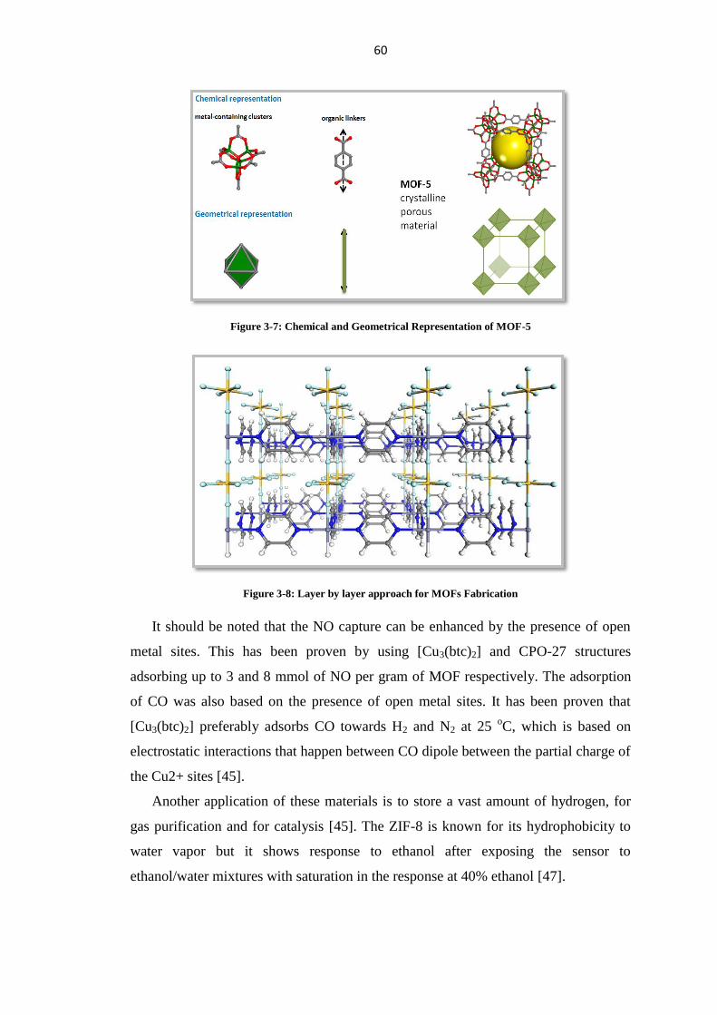
60
Figure 3-7: Chemical and Geometrical Representation of MOF-5
Figure 3-8: Layer by layer approach for MOFs Fabrication
It should be noted that the NO capture can be enhanced by the presence of open
metal sites. This has been proven by using [Cu3(btc)2] and CPO-27 structures
adsorbing up to 3 and 8 mmol of NO per gram of MOF respectively. The adsorption
of CO was also based on the presence of open metal sites. It has been proven that
[Cu3(btc)2] preferably adsorbs CO towards H2 and N2 at 25 oC, which is based on
electrostatic interactions that happen between CO dipole between the partial charge of
the Cu2+ sites [45].
Another application of these materials is to store a vast amount of hydrogen, for
gas purification and for catalysis [45]. The ZIF-8 is known for its hydrophobicity to
water vapor but it shows response to ethanol after exposing the sensor to
ethanol/water mixtures with saturation in the response at 40% ethanol [47].
61
MOF-5, IRMOF-3, MOF-177, IRMOF-62, Zn-CPO-27 and [Cu3(btc)2] has shown
high selectivity to tetrahydrothiophene, benzene, dichloromethane and ethylene
oxide [46]. For the [Cu3(btc)2] should be mentioned that the moisture diminish its
performance since the open metal sites are blocked my water molecules. Moreover,
MIL-101 has been validated to be very effective in the adsorption of VOCs and in a
large number of gases as acetone, benzene, toluene, ethylbenzene, xylenes, n-hexane,
methanol, butanone, dichloromethane and n-butylamine. MIL-53(Al) framework has
been proven effective in xylene isomers and ethylbenzene adsorption.
3.2.4 Polymers
A polymer is a large molecule, or macromolecule, composed of many repeated
subunits, known as monomers. The positive aspects of polymers as films are the high
sensitivity, short response times, room temperature operation, low power
consumption, which allow battery driven devices and low fabrication cost. On the
contrary, they suffer from long-time instability, irreversibility and poor selectivity.
Polymers often lack thermal or chemical stability and cannot be used as humidity
sensors in harsh environments. Moreover, they show slow hysteresis and long-term
drift in some solvents exposure [48]. There are two types of polymers based on the
changes in physical properties: conducting and non-conducting.
3.2.4.1 Conducting polymers
Conducting polymers’ conductivity is affected after their exposure either in
organic or inorganic gases. The most common are polypyrrole (PPy), polyaniline
(PAni), polythiophene (PTh) and their derivatives but cannot be used directly as gas
sensing material since their conductivity is too low. Different processes of doping by
redox reactions or protonation has been proven to increase the polymers conductivity.
This procedure transforms the polymers into conductors or semiconductors. During
the absorbing gas by the polymer, the doping level can be changed based on chemical
reactions providing a practical way of detection.
Analytically, a redox reaction is needed for a conducting polymer to be
doped/undoped. Hence, a variation in its doping level is achieved by transferring
electrons from or to the analytes. This can cause changes in resistance alternating the
sensing material. In some approaches, PPy, PTh and in some cases PAni films were
exposed to NH3, NO2, I2 and H2S [49]. NO2 and I2, as electron acceptors, can remove

62
electrons from the aromatic rings of conducting polymers, achieving enhancement in
the doping level of p-type conducting polymer. Of course, the opposite will occur in
electro-donating gas detection. For example, Ammonia, which is an electron-donor,
reacts with PPy and its electric resistance reduces sharply.
3.2.4.2 Non-Conducting polymers
Non-Conducting polymers are utilized for detecting changes in resonant
frequency or dielectric constant in capacitive, calometric or mass sensitive sensor
structures. These changes through the structures can be transformed into electrical
signal output. Another use of them is as an additive to metal oxide semiconductor gas
sensors as molecular sieves in order to enhance the sensitivity (e.g. polyimide).
Polymers are used extensively for detecting volatile organic compounds
(VOCs) [50], especially conductive, or solvent vapors in the gas phase, such as
alcohols, aromatic or halogenated compounds. Their sensitive properties rely on the
change in their dielectric properties by absorbing gas. In general, the gas detection
occurs at room temperature. They have also attracted the interest for their high
sensitivity and short response time.
There are many techniques for depositing the polymer in the sensor such as
Electrochemical deposition, coating (dip, spin, drop), Langmuir-Blodgett (LB), layer-
by-layer (LBL), thermal evaporation and vapor deposition polymerization [48][49].
The selection will be based on the uniformity, thickness and quality of the film.
3.2.5 Discussion
The aforementioned and analyzed film materials are concluded in Table 3-2,
where it can be easily observed that all of them have their positive and negative
aspects. Finally, the application is going to specify the necessary features and thus the
proper material will be selected.
The selectivity problems can be overcome with an electronic nose (e-nose), which
is a device with the intention of detecting odors or flavors. Since one gas sensor
cannot be selective in different concentration of gases, electronic noses usually utilize
arrays of sensors with different film material in order to detect different gases.
Moreover, the poor selectivity that can be also observed by using the arrays can be
overcome by using pattern recognition techniques in the processing of the results. The
feature that differentiates electronic noses from analytical instruments is that the first

63
can identify mixtures of samples as a whole, without having to identify individual
chemical species within the sample mixture.
Table 3-2: Advantages and disadvantages of the film materials
Materials Benefits Drawbacks
Metal Oxide
Semiconductor
Low-cost
Short Response time
Wide range of target gases
Long lifetime
Low selectivity and sensitivity
Rely on environmental factors
High energy consumption (heaters)
Carbon
Nanomaterials
Highly Selective
High adsorptive capacity
Short Response time
Difficulty in fabrication and
repeatability
High cost
Metal-Organic
Frameworks
Highly Selective
Highly Sensitive
Low energy consumption
High cost
Time consuming in fabrication
Polymers
High sensitivity
Short Response time
Low-cost
Low energy consumption
Instability
Irreversibility
3.3 Breath sensors
Breath sensors seem to have high potentials to act as biomarkers for detection and
monitoring of illnesses. Moreover, it can be a non-invasive way for health
diagnostics, replacing blood analysis and endoscopy. This will reduce the diagnostic
costs and it will provide a painless, fast and easy testing contributing to the life quality
improvement of the patients suffering from chronic diseases [51]. More specifically,
through clinical trials, the breath has shown potentials for the detection of illnesses as
different types of cancer, diabetes, multiple sclerosis, kidney disease and tuberculosis.
The exhaled breath has been detected to include, in decreasing order, nitrogen,
oxygen, carbon dioxide, water vapor, argon and a variety of approximately 3000
different VOC species appearing in ppb levels [51].
The diseases that can be detected through breath analysis can be separated into
two main categories [51] based on the VOCs origin:
a) Lungs: based on the effect of the disease on metabolic changes and oxidative
stress, which has an impact on the VOC blood content. In general, these VOCs
level is relatively low to the overall breath composition.
b) Cells and tissues: correlated to a health dysfunction and located next to
epithelium tissues in the respiratory system or the upper gastrointestinal tract.
64
Moreover, one important parameter that should be taken into careful consideration
is the operational temperature of the sensors. Specifically for breath samples, the
temperature should not be too high since there are compounds with possibility of
decomposition. This issue can either constrain the option in the sensors usage, by
avoiding metal-oxide films, or lead to local heating by using microheaters.
An application that can provide accurate information about breath analysis is still
a challenging issue. This is related to the fact that there are thousands of volatile
organic compounds (VOC) and their concentrations vary in the range of ppt to ppm.
The relation and the origin of the VOCs are still on a research level with some being
related to exogenous factors. Moreover, the exhalation time can vary per person since
it is relying on forced vital capacity (FVC) and expiratory flow, which can be related
to sex, age and health condition. Despite those facts, there are efforts, in research
level, in implementation of compact devices for solid and continuous measurements
in real time. For example, gas chromatography with flame ionization detection
(FID) [52], proton transfer reaction-mass spectrometry (PTR-MS) [53] selected ion
flow tube-mass spectrometry (SIFT-MS) [54] and differential mobility spectroscopy
(DMS) [55] have shown high selectivity, sufficient sensitivity and low limit of
detection for several VOCs. The disadvantage of the before-mentioned methods,
except DMS, is the high cost and lack of portability. Chemical gas sensors can
overcome these obstacles and become an appealing option [3].
More specifically, acetone has the potentials for being an indication of diabetes.
This is based on the fact that the concentration of acetone in healthy people breath
varies from 300 to 900 ppb and it is remarkably lower than for diabetics (more than
1800 ppb). Nonetheless, high acetone concentrations in a breath analysis cannot be
directly related to glucose levels in the blood, for which more research is
necessary [3].
A portable acetone sensor consisting of flame-deposited and in situ annealed; Si-
doped epsilon-WO3 nanostructured film was implemented [3] in a portable
device [28]. The response time of the sensor was below 15 sec. This film has shown
high sensitivity and selectivity to acetone even in high levels of relative humidity (up
to 90%). This gave the opportunity for simulating the human breath in a sense, which
has high levels of relative humidity (80% - 90%). The main drawback was the high
operational temperature (300 - 450 oC), which is a common characteristic of
chemoresistive gas sensors. In order to reach a reasonable level of power
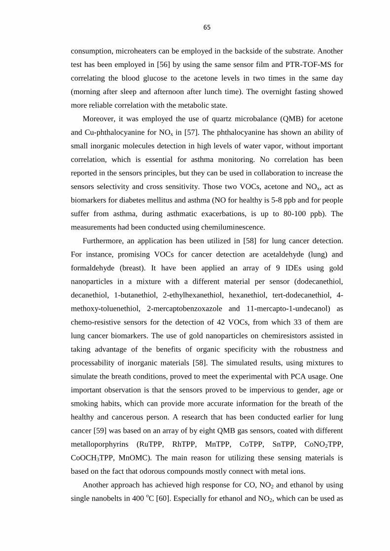
65
consumption, microheaters can be employed in the backside of the substrate. Another
test has been employed in [56] by using the same sensor film and PTR-TOF-MS for
correlating the blood glucose to the acetone levels in two times in the same day
(morning after sleep and afternoon after lunch time). The overnight fasting showed
more reliable correlation with the metabolic state.
Moreover, it was employed the use of quartz microbalance (QMB) for acetone
and Cu-phthalocyanine for NOx in [57]. The phthalocyanine has shown an ability of
small inorganic molecules detection in high levels of water vapor, without important
correlation, which is essential for asthma monitoring. No correlation has been
reported in the sensors principles, but they can be used in collaboration to increase the
sensors selectivity and cross sensitivity. Those two VOCs, acetone and NOx, act as
biomarkers for diabetes mellitus and asthma (NO for healthy is 5-8 ppb and for people
suffer from asthma, during asthmatic exacerbations, is up to 80-100 ppb). The
measurements had been conducted using chemiluminescence.
Furthermore, an application has been utilized in [58] for lung cancer detection.
For instance, promising VOCs for cancer detection are acetaldehyde (lung) and
formaldehyde (breast). It have been applied an array of 9 IDEs using gold
nanoparticles in a mixture with a different material per sensor (dodecanethiol,
decanethiol, 1-butanethiol, 2-ethylhexanethiol, hexanethiol, tert-dodecanethiol, 4-
methoxy-toluenethiol, 2-mercaptobenzoxazole and 11-mercapto-1-undecanol) as
chemo-resistive sensors for the detection of 42 VOCs, from which 33 of them are
lung cancer biomarkers. The use of gold nanoparticles on chemiresistors assisted in
taking advantage of the benefits of organic specificity with the robustness and
processability of inorganic materials [58]. The simulated results, using mixtures to
simulate the breath conditions, proved to meet the experimental with PCA usage. One
important observation is that the sensors proved to be impervious to gender, age or
smoking habits, which can provide more accurate information for the breath of the
healthy and cancerous person. A research that has been conducted earlier for lung
cancer [59] was based on an array of by eight QMB gas sensors, coated with different
metalloporphyrins (RuTPP, RhTPP, MnTPP, CoTPP, SnTPP, CoNO2TPP,
CoOCH3TPP, MnOMC). The main reason for utilizing these sensing materials is
based on the fact that odorous compounds mostly connect with metal ions.
Another approach has achieved high response for CO, NO2 and ethanol by using
single nanobelts in 400 oC [60]. Especially for ethanol and NO2, which can be used as
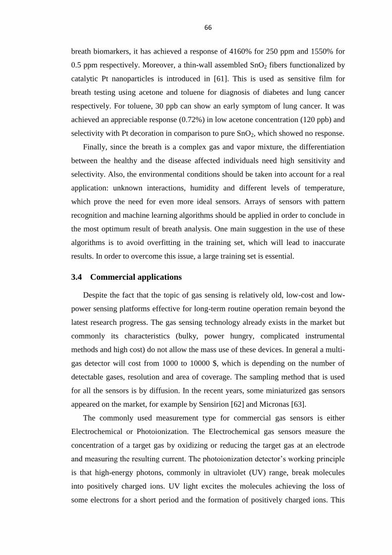
66
breath biomarkers, it has achieved a response of 4160% for 250 ppm and 1550% for
0.5 ppm respectively. Moreover, a thin-wall assembled SnO2 fibers functionalized by
catalytic Pt nanoparticles is introduced in [61]. This is used as sensitive film for
breath testing using acetone and toluene for diagnosis of diabetes and lung cancer
respectively. For toluene, 30 ppb can show an early symptom of lung cancer. It was
achieved an appreciable response (0.72%) in low acetone concentration (120 ppb) and
selectivity with Pt decoration in comparison to pure SnO2, which showed no response.
Finally, since the breath is a complex gas and vapor mixture, the differentiation
between the healthy and the disease affected individuals need high sensitivity and
selectivity. Also, the environmental conditions should be taken into account for a real
application: unknown interactions, humidity and different levels of temperature,
which prove the need for even more ideal sensors. Arrays of sensors with pattern
recognition and machine learning algorithms should be applied in order to conclude in
the most optimum result of breath analysis. One main suggestion in the use of these
algorithms is to avoid overfitting in the training set, which will lead to inaccurate
results. In order to overcome this issue, a large training set is essential.
3.4 Commercial applications
Despite the fact that the topic of gas sensing is relatively old, low-cost and low-
power sensing platforms effective for long-term routine operation remain beyond the
latest research progress. The gas sensing technology already exists in the market but
commonly its characteristics (bulky, power hungry, complicated instrumental
methods and high cost) do not allow the mass use of these devices. In general a multi-
gas detector will cost from 1000 to 10000 $, which is depending on the number of
detectable gases, resolution and area of coverage. The sampling method that is used
for all the sensors is by diffusion. In the recent years, some miniaturized gas sensors
appeared on the market, for example by Sensirion [62]and Micronas [63].
The commonly used measurement type for commercial gas sensors is either
Electrochemical or Photoionization. The Electrochemical gas sensors measure the
concentration of a target gas by oxidizing or reducing the target gas at an electrode
and measuring the resulting current. The photoionization detector’s working principle
is that high-energy photons, commonly in ultraviolet (UV) range, break molecules
into positively charged ions. UV light excites the molecules achieving the loss of
some electrons for a short period and the formation of positively charged ions. This

67
has a result in the gas, which is charged with the ions producing electric current as an
output in the detector. Thus, the higher is the concentration of the gas; the higher will
be the current. Some applications can be observed in Figure 3-9 - Figure 3-13 and
summarized in Table 3-3.
Figure 3-9: CO2 detector by
Greystone
Figure 3-10: VOCs detector by
RAE
Figure 3-11: VOCs detector by
ION
Figure 3-12: Gas Watch 2 by RKI
Figure 3-13: Multi gas detector by
RAE
Figure 3-14: Gas Sensor MQ-2
Table 3-3: Gas sensing applications
Sensor
Type
Range
(ppm)
Measurement
Type
Consumption/
Operating Time
Coverage
Area
Dimensions
(inch) Company
CO2 0 - 2000 NDIR 80 mA max 100 m² 5.7 x 3.9 x 2.5 Greystone
CO 0 - 300 Electrochemical 20 mA max 700 m² 2.8 x 4.1 x 1.8 Greystone
NO2 0 - 10 Electrochemical 50 mA max 700 m² 2.8 x 4.1 x 1.9 Greystone
VOCs 0 - 15000 Photoionization 12 hours with
alkaline battery - 10 x 3.0 x 2.5 RAE
VOCs 0 - 20000 Photoionization 3 x AA, up to 8.5
hours life -
13.4 x 3.6 x
2.4 ION
VOCs
CO
H2S
SO2
NO
NO2
HCN
NH3
HCl
HF
0 - 2000
0 - 2000
0 - 100
0 - 20
0 - 250
0-20
0-100
0-50
2 to 15
2 to 10
Photoionization
sensor for
VOCs
Electrochemical
sensors for
toxic gases
Up to 18 hours
continuous
operation
- 9.25 x 5.0 x
9.25 RAE
CO
H2S
0 - 500
0 - 100 Electrochemical
Over 3,000
hours -
2.8 x 3.3 x 1.2
(Watch size) GasWatch
by RKI

68
There are also available gas sensors for using them with famous microcontrollers,
as Arduino, and their price can vary from 3 to 35 $. They are using semiconductor
type of measurements, which is one of the reasons that are cheap enough. Their main
drawback is that preheating is needed for over 48 hours, which consumes power at
900mW. One of the gas sensors, which are included in Table 3-4, is illustrated in
Figure 3-14.
Table 3-4: Gas sensors
3.5 Gas sensing experiments
3.5.1 Utilized sensing films
The investigated films are based on the changes in the electrical properties, which
can be depicted in the structure’s capacitance. The capacitor was selected as
transducer since there is no DC power dissipation and it needs a simple circuit
interface for the read out. These sensors operate with the absorption mechanism
where the film material in the structure will have a variance in its permittivity by
applying different gases. For this work, the Polyimide and Nafion polymers and the
Cu(bdc).xH2O MOF were evaluated for their gas sensing properties. They were
selected based on the fact that they can operate in room temperature and thus no
heating is needed.
3.5.1.1 Polyimide
Polyimide (PI) is a commonly used polymer in many everyday applications,
which consists of imide monomers, which is illustrated in Figure 3-15. Its popularity
is based on its properties: high strength, thermal stability and chemical resistant, high
density and viscosity, high heat-resistance. In order to clarify the importance of its
characteristics, it is common in applications to replace glass and metals.
Detection Gas Measurement
Type
Concentration
(ppm)
Preheat
time No
Price
($)
Ammonia/
Sulfide/
Benzene steam
Semiconductor 10-10000 > 48 h MQ135 3.85
SO2 Semiconductor 1-200 > 48 h MQ136 34,99
NH3 Semiconductor 5-500 > 48 h MQ137 31.95
Toluene/
Acetone
Ethanol
Semiconductor 5-500 > 48 h MQ138 29,99
CO Semiconductor 10-10000 > 48 h MQ-7 7.25
CH4
H2 Semiconductor
5000-20000
300-5000 > 24 h MQ-2 8.95
69
Figure 3-15: Representation of Imide monomer chemical structure
PI has been used as sensitive material for biosensors, humidity [64], gas, tactile
and pressure sensors [65]. In our work, the PI-2611 that was utilized, it is a polyimide
with low moisture, low stress (CTE = 5 ppm) and high modulus of elasticity (8.5
GPa).
The sensor has been immersed in a mixture 1:1000 of Adhesion promoter:DI H2O
for enhancing the adhesion of PI. Then, the PI film was spin-coated with speed of 500
rpm for 5 sec and 3500 rpm for 30sec. Then, it was annealed at 90oC for 90 sec and
150oC for 90 sec.
3.5.1.2 Nafion
Nafion is a sulfonated tetrafluoroethylene based fluoropolymer-copolymer
produced and developed by the DuPont Company. The process of implementing this
material is the copolymerization of a perfluorinated vinyl ether comonomer with
tetrafluoroethylene (TFE) [66]. The molecular formula is C7HF13O5S.C2F4 and the
chemical structure is depicted in Figure 3-16.
Figure 3-16: Representation of Nafion’s Chemical structure
The main application of Nafion was through its use as a proton conductor for
proton exchange membrane (PEM) fuel cells and water electrolytes. This is based on
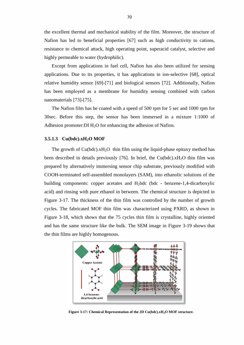
70
the excellent thermal and mechanical stability of the film. Moreover, the structure of
Nafion has led to beneficial properties [67] such as high conductivity to cations,
resistance to chemical attack, high operating point, superacid catalyst, selective and
highly permeable to water (hydrophilic).
Except from applications in fuel cell, Nafion has also been utilized for sensing
applications. Due to its properties, it has applications in ion-selective [68], optical
relative humidity sensor [69]-[71] and biological sensors [72]. Additionally, Nafion
has been employed as a membrane for humidity sensing combined with carbon
nanomaterials [73]-[75].
The Nafion film has be coated with a speed of 500 rpm for 5 sec and 1000 rpm for
30sec. Before this step, the sensor has been immersed in a mixture 1:1000 of
Adhesion promoter:DI H2O for enhancing the adhesion of Nafion.
3.5.1.3 Cu(bdc).xH2O MOF
The growth of Cu(bdc).xH2O thin film using the liquid-phase epitaxy method has
been described in details previously [76]. In brief, the Cu(bdc).xH2O thin film was
prepared by alternatively immersing sensor chip substrate, previously modified with
COOH-terminated self-assembled monolayers (SAM), into ethanolic solutions of the
building components: copper acetates and H2bdc (bdc - benzene-1,4-dicarboxylic
acid) and rinsing with pure ethanol in between. The chemical structure is depicted in
Figure 3-17. The thickness of the thin film was controlled by the number of growth
cycles. The fabricated MOF thin film was characterized using PXRD, as shown in
Figure 3-18, which shows that the 75 cycles thin film is crystalline, highly oriented
and has the same structure like the bulk. The SEM image in Figure 3-19 shows that
the thin films are highly homogenous.
Figure 3-17: Chemical Representation of the 2D Cu(bdc).xH2O MOF structure.

71
Figure 3-18: XRPD of Cu(BDC).xH2O MOF thin film
Figure 3-19: SEM of Cu(bdc).xH2O film
3.5.2 Relative Humidity Experiments
For the humidity testing of the sensors, two different experiments were conducted.
The first, purge experiment, was purging in between the steps. The relative humidity
level was varying by changing with a step of 50 sccm the carrier flow of the bubbler’s
inlet and dilution of dry Nitrogen from 0 sccm to 200 sccm and from 200 sccm to 0
sccm respectively. The second experiment was an increasing ramp of relative
humidity without purging in between the steps. The carrier and dilution flow were
ranging with a step of 25 from 0 sccm to 200 sccm and 200 to 0 sccm respectively
sccm. Both experiments are superimposed in Figure 3-20 for the commercial sensor.
Figure 3-20: Ramp and Purge Experiment for HIH-4000 Sensor
The purging experiment was repeated three times to prove the reproducibility of
the results. The time for having a saturated value was different depending on the
material and the experiment. For Polyimide, since it has high density, the time per
step was 15 minutes for ramp and 20 minutes for purge. For the Nafion and
0
20
40
60
80
100
0 20 40 60 80 100
Hum
idit
y (
RH
%)
Time (min)
Ramp
Purge
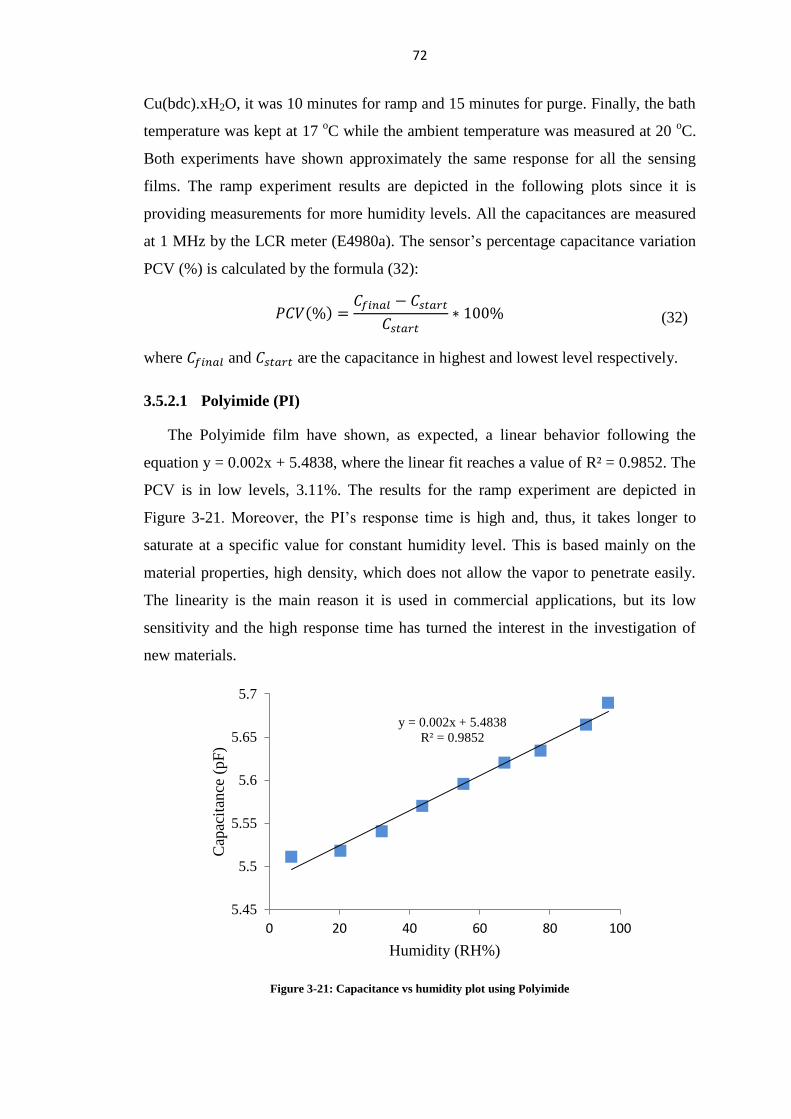
72
Cu(bdc).xH2O, it was 10 minutes for ramp and 15 minutes for purge. Finally, the bath
temperature was kept at 17 oC while the ambient temperature was measured at 20
oC.
Both experiments have shown approximately the same response for all the sensing
films. The ramp experiment results are depicted in the following plots since it is
providing measurements for more humidity levels. All the capacitances are measured
at 1 MHz by the LCR meter (E4980a). The sensor’s percentage capacitance variation
PCV (%) is calculated by the formula (32):
𝑃𝐶𝑉(%) =𝐶𝑓𝑖𝑛𝑎𝑙 − 𝐶𝑠𝑡𝑎𝑟𝑡
𝐶𝑠𝑡𝑎𝑟𝑡∗ 100% (32)
where 𝐶𝑓𝑖𝑛𝑎𝑙 and 𝐶𝑠𝑡𝑎𝑟𝑡 are the capacitance in highest and lowest level respectively.
3.5.2.1 Polyimide (PI)
The Polyimide film have shown, as expected, a linear behavior following the
equation y = 0.002x + 5.4838, where the linear fit reaches a value of R² = 0.9852. The
PCV is in low levels, 3.11%. The results for the ramp experiment are depicted in
Figure 3-21. Moreover, the PI’s response time is high and, thus, it takes longer to
saturate at a specific value for constant humidity level. This is based mainly on the
material properties, high density, which does not allow the vapor to penetrate easily.
The linearity is the main reason it is used in commercial applications, but its low
sensitivity and the high response time has turned the interest in the investigation of
new materials.
Figure 3-21: Capacitance vs humidity plot using Polyimide
y = 0.002x + 5.4838
R² = 0.9852
5.45
5.5
5.55
5.6
5.65
5.7
0 20 40 60 80 100
Cap
acit
ance
(pF
)
Humidity (RH%)

73
3.5.2.2 Nafion
As can be observed in Figure 3-22, the humidity follows a linear behavior with
two separate curves, one for a ramp below 65% and another over this limit. The PCV
that can be achieved until 64.4% and in overall is 571%. This can prove the Nafion as
an indicator of excessive humidity levels. For the levels over 65%, the film absorbs
larger amount of water vapor, which can be observed by the increase of the
dissipation factor. The reproducibility of the results in Figure 3-23 proved the
operation of the sensor in two regions. There is an accurate (R² = 0.9947) slight
polynomial behavior of second order (y = 0.001x2 - 0.0245x + 4.6736) until the level
of 65% of RH. After this level, the behavior is becoming polynomial with a
considerable increase in the 2nd
order of it (y = 0.0178x2 - 2.0957x + 67.861), proving
the important increase in the range. This fact is based on the hydrophilicity of Nafion.
Figure 3-22: Capacitance vs humidity plot using Nafion
Figure 3-23: Results Reproducibility of Nafion Film For purging Experiment
y = 0.001x2 - 0.0245x + 4.6736
R² = 0.9947
y = 0.0178x2 - 2.0957x + 67.861
R² = 0.9992
0
5
10
15
20
25
30
35
0 20 40 60 80 100
Cap
acit
ance
(pF
)
Humidity (RH%)
Ramp below 65%
Ramp over 65%
0
10
20
30
40
50
0 20 40 60 80 100
Cap
acit
ance
(pF
)
Time (min)
1st experiment
2nd experiment
3rd experiment
RH 30% RH 50%
RH 70%
RH 90%
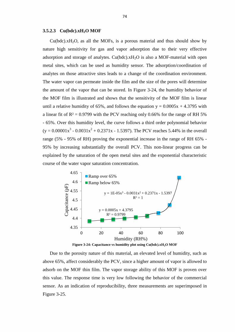
74
3.5.2.3 Cu(bdc).xH2O MOF
Cu(bdc).xH2O, as all the MOFs, is a porous material and thus should show by
nature high sensitivity for gas and vapor adsorption due to their very effective
adsorption and storage of analytes. Cu(bdc).xH2O is also a MOF-material with open
metal sites, which can be used as humidity sensor. The adsorption/coordination of
analytes on those attractive sites leads to a change of the coordination environment.
The water vapor can permeate inside the film and the size of the pores will determine
the amount of the vapor that can be stored. In Figure 3-24, the humidity behavior of
the MOF film is illustrated and shows that the sensitivity of the MOF film is linear
until a relative humidity of 65%, and follows the equation y = 0.0005x + 4.3795 with
a linear fit of R² = 0.9799 with the PCV reaching only 0.66% for the range of RH 5%
- 65%. Over this humidity level, the curve follows a third order polynomial behavior
(y = 0.00001x3 - 0.0031x
2 + 0.2371x - 1.5397). The PCV reaches 5.44% in the overall
range (5% - 95% of RH) proving the exponential increase in the range of RH 65% -
95% by increasing substantially the overall PCV. This non-linear progress can be
explained by the saturation of the open metal sites and the exponential characteristic
course of the water vapor saturation concentration.
Figure 3-24: Capacitance vs humidity plot using Cu(bdc).xH2O MOF
Due to the porosity nature of this material, an elevated level of humidity, such as
above 65%, affect considerably the PCV, since a higher amount of vapor is allowed to
adsorb on the MOF thin film. The vapor storage ability of this MOF is proven over
this value. The response time is very low following the behavior of the commercial
sensor. As an indication of reproducibility, three measurements are superimposed in
Figure 3-25.
y = 1E-05x3 - 0.0031x2 + 0.2371x - 1.5397
R² = 1
y = 0.0005x + 4.3795
R² = 0.9799
4.35
4.4
4.45
4.5
4.55
4.6
4.65
0 20 40 60 80 100
Cap
acit
ance
(pF
)
Humidity (RH%)
Ramp over 65%
Ramp below 65%
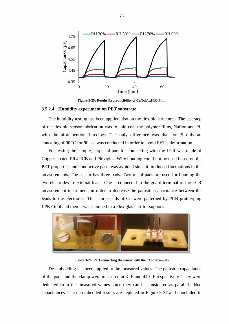
75
Figure 3-25: Results Reproducibility of Cu(bdc).xH2O Film
3.5.2.4 Humidity experiment on PET substrate
The humidity testing has been applied also on the flexible structures. The last step
of the flexible sensor fabrication was to spin coat the polymer films, Nafion and PI,
with the aforementioned recipes. The only difference was that for PI only an
annealing of 90 oC for 90 sec was conducted in order to avoid PET’s deformation.
For testing the sample, a special part for connecting with the LCR was made of
Copper coated FR4 PCB and Plexiglas. Wire bonding could not be used based on the
PET properties and conductive paste was avoided since it produced fluctuations in the
measurements. The sensor has three pads. Two metal pads are used for bonding the
two electrodes to external leads. One is connected to the guard terminal of the LCR
measurement instrument, in order to decrease the parasitic capacitance between the
leads to the electrodes. Thus, three pads of Cu were patterned by PCB prototyping
LPKF tool and then it was clamped in a Plexiglas part for support.
Figure 3-26: Part connecting the sensor with the LCR terminals
De-embedding has been applied to the measured values. The parasitic capacitance
of the pads and the clamp were measured at 3 fF and 440 fF respectively. They were
deducted from the measured values since they can be considered as parallel-added
capacitances. The de-embedded results are depicted in Figure 3-27 and concluded in
4.35
4.45
4.55
4.65
4.75
0 20 40 60
Cap
acit
ance
(pF
)
Time (min)
RH 30% RH 50% RH 70% RH 90%
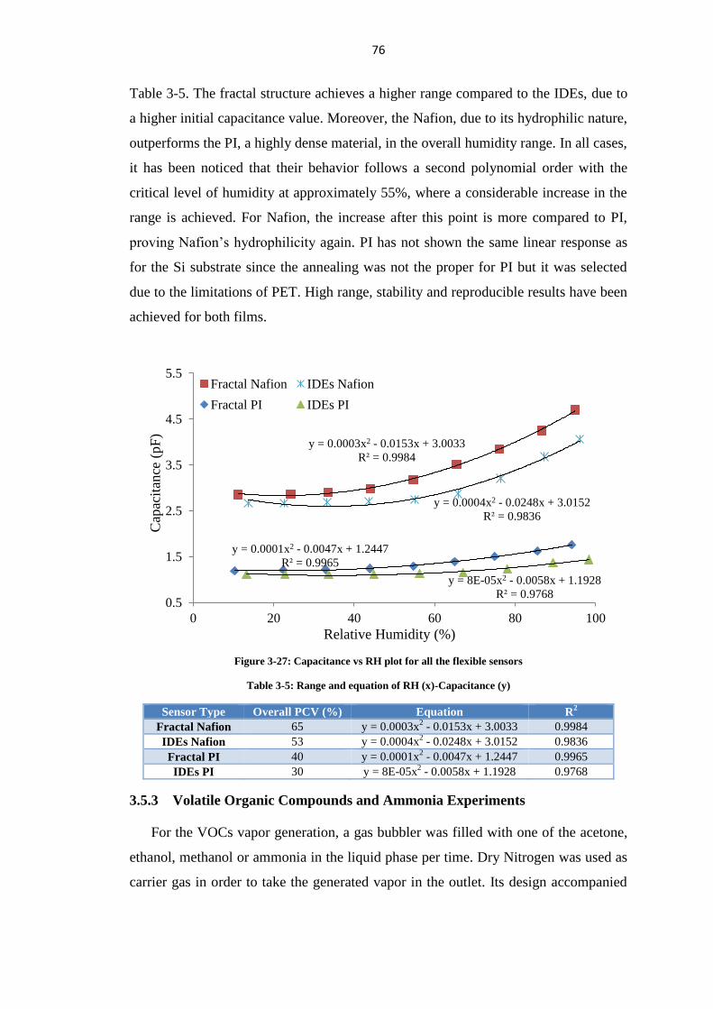
76
Table 3-5. The fractal structure achieves a higher range compared to the IDEs, due to
a higher initial capacitance value. Moreover, the Nafion, due to its hydrophilic nature,
outperforms the PI, a highly dense material, in the overall humidity range. In all cases,
it has been noticed that their behavior follows a second polynomial order with the
critical level of humidity at approximately 55%, where a considerable increase in the
range is achieved. For Nafion, the increase after this point is more compared to PI,
proving Nafion’s hydrophilicity again. PI has not shown the same linear response as
for the Si substrate since the annealing was not the proper for PI but it was selected
due to the limitations of PET. High range, stability and reproducible results have been
achieved for both films.
Figure 3-27: Capacitance vs RH plot for all the flexible sensors
Table 3-5: Range and equation of RH (x)-Capacitance (y)
Sensor Type Overall PCV (%) Equation R2
Fractal Nafion 65 y = 0.0003x2 - 0.0153x + 3.0033 0.9984
IDEs Nafion 53 y = 0.0004x2 - 0.0248x + 3.0152 0.9836
Fractal PI 40 y = 0.0001x2 - 0.0047x + 1.2447 0.9965
IDEs PI 30 y = 8E-05x2 - 0.0058x + 1.1928 0.9768
3.5.3 Volatile Organic Compounds and Ammonia Experiments
For the VOCs vapor generation, a gas bubbler was filled with one of the acetone,
ethanol, methanol or ammonia in the liquid phase per time. Dry Nitrogen was used as
carrier gas in order to take the generated vapor in the outlet. Its design accompanied
y = 0.0003x2 - 0.0153x + 3.0033
R² = 0.9984
y = 0.0004x2 - 0.0248x + 3.0152
R² = 0.9836
y = 0.0001x2 - 0.0047x + 1.2447
R² = 0.9965
y = 8E-05x2 - 0.0058x + 1.1928
R² = 0.9768 0.5
1.5
2.5
3.5
4.5
5.5
0 20 40 60 80 100
Cap
acit
ance
(pF
)
Relative Humidity (%)
Fractal Nafion IDEs Nafion
Fractal PI IDEs PI

77
with the steady flow of the MFCs is providing a uniform flow of vapor generation.
The calculation of the output flow is based on the equation (33) [77]:
𝐹𝑜𝑢𝑡 = (𝑎 + 1)𝐹𝑐 (33)
where 𝐹𝑜𝑢𝑡 is the output flow, 𝐹𝑐 is the carrier flow, 𝑎 is the ratio of the saturated
thermodynamic vapor pressure (𝑃𝑜𝑢𝑡) to the input pressure (𝑃𝑖), which can be
calculated from Antoine’s equation for the bath and ambient temperature. The process
of vapor generation is illustrated in Figure 3-28.
The generated vapor was diluted with dry Nitrogen before being inserted into the
testing chamber. The final concentration in parts per million can be calculated by the
equation (34):
𝐶𝑝𝑝𝑚 = 𝑎𝐹𝑐
𝐹𝑑 + (𝑎 + 1)𝐹𝑐× 106
(34)
Figure 3-28: Vapor generation process
Different concentrations can be achieved by varying either the bath temperature
or/and the flow rate of the bubbler as it can be observed from (33). The purge
experiment for acetone, ethanol and methanol was utilized by varying the flow rate
for the carrier from 0 to 10 sccm and the dilution (𝐹𝑑) from 200 to 190 sccm with a
step of 2.5 sccm. For ammonia, since lower concentrations were desired, a mixture of
water and ammonia (30%) was employed and the carrier flow rate was varying from
0.15 to 0.6 sccm with a step of 0.15 sccm. A gas cylinder was utilized with diluted
toluene in Nitrogen in a concentration of 500 ppm. The experiment was based on
varying the gas from 0 sccm to 200 sccm with a step of 50 sccm respectively. The
dilution flow was acting complementarily to carrier in order their summation to be
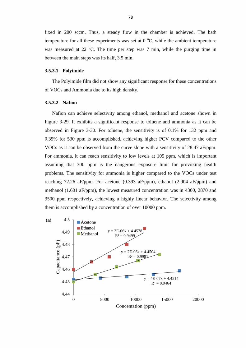
78
fixed in 200 sccm. Thus, a steady flow in the chamber is achieved. The bath
temperature for all these experiments was set at 0 oC, while the ambient temperature
was measured at 22 oC. The time per step was 7 min, while the purging time in
between the main steps was its half, 3.5 min.
3.5.3.1 Polyimide
The Polyimide film did not show any significant response for these concentrations
of VOCs and Ammonia due to its high density.
3.5.3.2 Nafion
Nafion can achieve selectivity among ethanol, methanol and acetone shown in
Figure 3-29. It exhibits a significant response to toluene and ammonia as it can be
observed in Figure 3-30. For toluene, the sensitivity is of 0.1% for 132 ppm and
0.35% for 530 ppm is accomplished, achieving higher PCV compared to the other
VOCs as it can be observed from the curve slope with a sensitivity of 28.47 aF/ppm.
For ammonia, it can reach sensitivity to low levels at 105 ppm, which is important
assuming that 300 ppm is the dangerous exposure limit for provoking health
problems. The sensitivity for ammonia is higher compared to the VOCs under test
reaching 72.26 aF/ppm. For acetone (0.393 aF/ppm), ethanol (2.904 aF/ppm) and
methanol (1.601 aF/ppm), the lowest measured concentration was in 4300, 2870 and
3500 ppm respectively, achieving a highly linear behavior. The selectivity among
them is accomplished by a concentration of over 10000 ppm.
y = 4E-07x + 4.4514
R² = 0.9464
y = 3E-06x + 4.4578
R² = 0.9499
y = 2E-06x + 4.4504
R² = 0.9981
4.44
4.45
4.46
4.47
4.48
4.49
4.5
0 5000 10000 15000 20000
Cap
acit
ance
(pF
)
Concentation (ppm)
Acetone
Ethanol
Methanol
(a)

79
Figure 3-29: Nafion response to acetone, ethanol and methanol concentrations
Figure 3-30: Nafion response to toluene and ammonia concentrations
y = 1E-05x - 0.0344
R² = 0.9511
y = 7E-05x - 0.126
R² = 0.9513
y = 3E-05x + 0.0204
R² = 0.9981
0
0.2
0.4
0.6
0.8
0 5000 10000 15000 20000
PC
V (
%)
Concentation (ppm)
Acetone
Ethanol
Methanol
y = 3E-05x + 4.4661
R² = 0.9979
y = 7E-05x + 4.4694
R² = 0.9821
4.46
4.47
4.48
4.49
4.5
4.51
0 100 200 300 400 500 600
Cap
acit
ance
(pF
)
Concentation (ppm)
Toluene
Ammonia
y = 0.0014x + 0.108
R² = 0.9912
y = 0.0006x + 0.0112
R² = 0.9956
0
0.2
0.4
0.6
0.8
1
0 100 200 300 400 500 600
PC
V (
%)
Concentation (ppm)
Ammonia
Toluene
(a)
(b)
(b)

80
3.5.3.3 Cu(bdc).xH2O MOF
Cu(bdc).xH2O showed linear behavior for acetone, ethanol and methanol as it can
be observed from Figure 3-31. However, the responses for the three vapors are
similar, which is due to the similarity in the chemical nature and size of their
molecules. Moreover, MOF also had a linear response to toluene, as it can be
observed in Figure 3-32, which was tested in very low concentrations, 125-500 ppm.
For ammonia, it managed to detect the concentration range of 105 - 492 ppm. The
MOF is more sensitive to ammonia (7.957 aF/ppm) and toluene (8.1137 aF/ppm)
compared to other VOCs, acetone (0.167 aF/ppm), ethanol (0.342 aF/ppm) and
methanol (0.218 aF/ppm). This occurs since ammonia and toluene react with the
organic part of it. Thus, there is also a slight increase in the overall capacitance even
after extensive N2 purging. Therefore, Cu(bdc).xH2O, can be considered as a detector
for VOCs, without achieving selectivity among them.
Figure 3-31: MOF response to acetone, ethanol and methanol concentrations
y = 2E-07x + 4.4207
R² = 0.9836
y = 3E-07x + 4.3703
R² = 0.9861
y = 2E-07x + 4.4058
R² = 0.9664
4.35
4.37
4.39
4.41
4.43
4.45
0 5000 10000 15000 20000
Cap
acit
ance
(pF
)
Concentation (ppm)
AcetoneEthanolMethanol
y = 5E-06x + 0.0052
R² = 0.9806 y = 8E-06x - 0.0003
R² = 1
y = 6E-06x - 0.0139
R² = 0.9872
0
0.02
0.04
0.06
0.08
0.1
0 5000 10000 15000 20000
PC
V (
%)
Concentation (ppm)
Acetone
Ethanol
Methanol
(a)
(b)

81
Figure 3-32: MOF response to toluene and ammonia concentrations
3.5.4 Discussion
The response and recovery time cannot be accurately calculated since the system
has a maximum fixed allowed flow and the chamber needs a considerable time of 3 to
4 min approximately to reach from a level of 10% to a level of 90%. Despite that fact,
it can be evaluated how fast the response of the sensor is by comparing it to the
commercial one. It has been proven that Nafion and Cu(bdc).xH2O have an almost
simultaneous reaction to humidity change following the response of the commercial
sensor. On the other hand, the Polyimide seems to be more reluctant to changes and it
is responding to a slower pace compared to the other films. The relative humidity
sensitivity for each material is summarized in Table 3-6. As it can be easily observed,
y = 8E-06x + 4.4776
R² = 0.9996
y = 8E-06x + 4.4444
R² = 0.9669
4.44
4.45
4.46
4.47
4.48
4.49
0 100 200 300 400 500 600
Cap
acit
ance
(pF
)
Concentation (ppm)
Toluene
Ammonia
y = 0.0002x + 0.0127
R² = 0.959
y = 0.0001x + 0.0056
R² = 0.9947
0
0.02
0.04
0.06
0.08
0.1
0 100 200 300 400 500 600
PC
V(%
)
Concentation (ppm)
Ammonia
Toluene
(a)
(b)
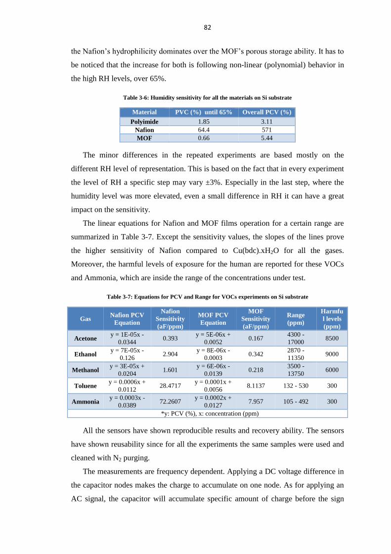
82
the Nafion’s hydrophilicity dominates over the MOF’s porous storage ability. It has to
be noticed that the increase for both is following non-linear (polynomial) behavior in
the high RH levels, over 65%.
Table 3-6: Humidity sensitivity for all the materials on Si substrate
Material PVC (%) until 65% Overall PCV (%)
Polyimide 1.85 3.11
Nafion 64.4 571
MOF 0.66 5.44
The minor differences in the repeated experiments are based mostly on the
different RH level of representation. This is based on the fact that in every experiment
the level of RH a specific step may vary ±3%. Especially in the last step, where the
humidity level was more elevated, even a small difference in RH it can have a great
impact on the sensitivity.
The linear equations for Nafion and MOF films operation for a certain range are
summarized in Table 3-7. Except the sensitivity values, the slopes of the lines prove
the higher sensitivity of Nafion compared to Cu(bdc).xH2O for all the gases.
Moreover, the harmful levels of exposure for the human are reported for these VOCs
and Ammonia, which are inside the range of the concentrations under test.
Table 3-7: Equations for PCV and Range for VOCs experiments on Si substrate
Gas Nafion PCV
Equation
Nafion
Sensitivity
(aF/ppm)
MOF PCV
Equation
MOF
Sensitivity
(aF/ppm)
Range
(ppm)
Harmfu
l levels
(ppm)
Acetone y = 1E-05x -
0.0344 0.393
y = 5E-06x +
0.0052 0.167
4300 -
17000 8500
Ethanol y = 7E-05x -
0.126 2.904
y = 8E-06x -
0.0003 0.342
2870 -
11350 9000
Methanol y = 3E-05x +
0.0204 1.601
y = 6E-06x -
0.0139 0.218
3500 -
13750 6000
Toluene y = 0.0006x +
0.0112 28.4717
y = 0.0001x +
0.0056 8.1137 132 - 530 300
Ammonia y = 0.0003x -
0.0389 72.2607
y = 0.0002x +
0.0127 7.957 105 - 492 300
*y: PCV (%), x: concentration (ppm)
All the sensors have shown reproducible results and recovery ability. The sensors
have shown reusability since for all the experiments the same samples were used and
cleaned with N2 purging.
The measurements are frequency dependent. Applying a DC voltage difference in
the capacitor nodes makes the charge to accumulate on one node. As for applying an
AC signal, the capacitor will accumulate specific amount of charge before the sign

83
change of the potential difference and the charge dissipates. The higher the frequency,
the less charge will accumulate and the smaller the opposition to the current. Reading
capacitance in low frequencies provides long time for water dipoles to orient to a
large extent in the material. Hence, the adsorbed water molecules in the sensitive film
can be more polarized at lower frequencies and by increasing the readout frequency,
they become less polarized. This fact can explain the humidity testing results as they
are concluded in the Table 3-8.
Table 3-8: Sensitivity (pF/RH) of the tested materials in different frequencies for the humidity testing
Material RH% 1 kHz 10 kHz 100 kHz 1 MHz
PI 8 - 96 0.00852 0.003517 0.002355 0.001978
MOF
8 - 66
66 - 89
89 - 98
0.001363
0.018927
0.148833
0.000941
0.007301
0.056058
0.000669
0.004136
0.027146
0.000498
0.002619
0.015644
Nafion 8 - 66
66 - 95
132.3705
609.7299
13.41511
402.7637
0.598738
44.62289
0.050449
0.776215
It is considered important to compare the measured results with the state of the art
or commercially available capacitive sensors. As it can be seen comparing the results
from the Table 3-8 to the Table 3-9 and Table 3-10, Nafion shows high sensitivity in
humidity. The only material that has achieved a higher sensitivity is described in [81],
where SiC nanowires are used as a sensitive film. Moreover, Nafion has shown higher
sensitivity compared to the commercial application, which proves again its
hydrophilicity. It should also be noted that Polyimide and MOF are less sensitive
compared to the other mentioned materials in Table 3-9 and commercial sensors in
Table 3-10. The only exception is for Polyimide compared to [80], where it surpasses
the sensitivity values of those Polyimide sensors but it is still below the sensitivity for
the Polyimide mentioned in [83].
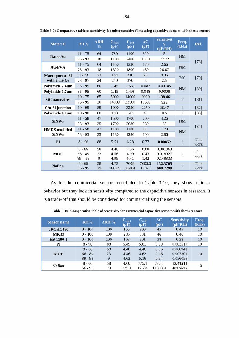
84
Table 3-9: Comparative table of sensitivity for other sensitive films using capacitive sensors with thesis sensors
Material RH% ΔRH
%
Cstart
(pF)
Cend
(pF)
ΔC
(pF)
Sensitivit
y
(pF/RH)
Freq.
(kHz) Ref.
Nano Au 11 - 75 64 780 1100 320 5
NM
[78] 75 - 93 18 1100 2400 1300 72.22
Au-PVA 11 - 75 64 1150 1320 170 2.66
NM 75 - 93 18 1320 1800 480 26.67
Macroporous Si
with a Ta2O5
0 - 73 73 184 210 26 0.36 200 [79]
73 - 97 24 210 270 60 2.5
Polyimide 2.4um 35 - 95 60 1.45 1.537 0.087 0.00145 NM [80]
Polyimide 1.7um 35 - 95 60 1.45 1.498 0.048 0.0008
SiC nanowires 10 - 75 65 5000 14000 9000 138.46
1 [81] 75 - 95 20 14000 32500 18500 925
C/n-Si junction 10 - 95 85 1000 3250 2250 26.47 1 [82]
Polyimide 0.1um 10 - 90 80 103 143 40 0.5 1 [83]
SiNWs 11 - 58 47 1500 1700 200 4.26
NM
[84] 58 - 93 35 1700 2680 980 28
HMDS modified
SiNWs
11 - 58 47 1100 1180 80 1.70 NM
58 - 93 35 1180 1280 100 2.86
PI 8 – 96 88 5.51 6.28 0.77 0.00852 1 This
work
MOF
8 - 66
66 - 89
89 – 98
58
23
9
4.48
4.56
4.99
4.56
4.99
6.41
0.08
0.43
1.42
0.001363
0.018927
0.148833
1 This
work
Nafion 8 - 66
66 - 95
58
29
4.73
7607.5
7608
25484
7603.3
17876 132.3705
609.7299 1
This
work
As for the commercial sensors concluded in Table 3-10, they show a linear
behavior but they lack in sensitivity compared to the capacitive sensors in research. It
is a trade-off that should be considered for commercializing the sensors.
Table 3-10: Comparative table of sensitivity for commercial capacitive sensors with thesis sensors
Sensor name RH% ΔRH % Cstart
(pF)
Cend
(pF)
ΔC
(pF)
Sensitivity
(pF/RH)
Freq.
(kHz)
JRCHC180 0 - 100 100 155 200 45 0.45 10
MK33 0 - 100 100 285 331 46 0.46 10
HS 1100-1 0 - 100 100 163 201 38 0.38 10
PI 8 - 96 88 5.49 5.81 0.39 0.003517 10
MOF
8 - 66
66 - 89
89 - 98
58
23
9
4.40
4.46
4.62
4.46
4.62
5.16
0.06
0.16
0.54
0.000941
0.007301
0.056058
10
Nafion 8 - 66
66 - 95
58
29
4.60
775.1
775.1
12584
770.5
11808.9 13.41511
402.7637 10
85
Chapter 4: Biological sensing
Biosensor is commonly defined as: “a chemical sensing device in which a
biologically derived recognition entity is coupled to a transducer, to allow the
quantitative development of some complex biochemical parameter” [85]. A biosensor,
as most of the sensors, consists of two main parts: the transducer and the electronics
part. In the transducer part, there is a receptor (e.g. nucleic acids, cells, antibodies,
enzymes), where biological analyte will specifically bind, and the electrical interface
(e.g. nanowire array, FET, electrodes), where the signal is generated and transformed
into electrical. The electronic part, amplifies firstly this signal, if it is weak, and then
it is processed.
The standards that a biosensor should meet for potential commercialization, as
mentioned in [86], are:
(a) High specificity in the biocatalyst, which shows stability under normal
conditions and no important difference between assays.
(b) Impervious to conditions as humidity, temperature and pH, which will assist to
avoid any pre-treatment, which will increase the complexity.
(c) Reproducible and accurate results.
(d) Non or the least possible invasive monitoring with biocompatibility without
having any negative impact on the object under test.
(e) Decreased assay time and the possibility of real time analysis are more
preferable.
(f) Low-cost, portability and easy in usage.
Nowadays, although there is a wide variety of devices that can be used as
biosensors for diagnosis in vivo testing, only glucose sensor meets the before
mentioned requirements. Dealing with biological analytes, it is still challenging to
provide high specificity and reproducibly in a portable low-cost device without a
doctor’s supervision.
There is a need for quantifying biological or biochemical processes but the
sensing track is still a challenging field. It is a complex process to achieve
transforming the biological procedure in an electrical signal. There are many types of
biosensors which include bioluminescent, electrochemical (e.g. amperometric,
conductometric, potentiometric), optoelectronic (e.g. resonant mirror, fiber optic,
surface plasmon resonance) and piezoelectric (e.g. crystal resonance frequency,

86
surface acoustic wave) [87]. All these methods can provide information for biological
sensing utilizing a different physical principle. Electrochemical biological sensors are
capable of transforming directly the biological information into an electrical signal.
This fact leads to lower setup complexity in the information extraction. Moreover,
they are robust and compatible with microelectronic circuits. This fact leads to a
decrease in cost and size. Thus, it has attracted interest either by using it alone or
assisting the previously mentioned methods. On the other hand, the negative aspect is
that the surface architectures suffer from achieving considerable sensitivity and high
specificity in the desired biochemical event [86].
Immunoassays are crucial and versatile analytical tools with a wide range of
application in the biomedical field. Efforts are made by researchers to detect
ultrasensitive [88], label-free [89] simple and high throughput [90] assays. Small
amounts of biomarkers are detected via quantitative immunoassays in physiological
fluids [91] also these are assays used when screened for environmental
contaminants [92], screened for infectious or toxic substances [93], monitored for
therapeutic drugs [94]. Traditional assays like cards and slides or conventional assays
that are usually performed in micro-well plates have several demerits that include
complexities in fluids handling, requirement for large sample volumes and increased
assay time. These demerits have limited the use of traditional and conventional
systems in diagnostics [95][96][97]. Therefore, there is a need for developing a low-
cost point-of-care device with a decreased assay time compared to the current
technology. Two experiments for proteins, CRP and BSA, quantification were
conducted by using capacitive structures.
4.1 Capacitive immunosensor to quantify C-reactive protein
C-reactive protein (CRP) is an acute-phase serum protein and a member of the
pentraxin protein family. C-reactive protein (CRP), the prototypical acute-phase
protein, has a mass of 120 kDa and is composed of five identical polypeptide subunits
held together by noncovalent interactions.
Its host defense functions predate the adaptive immune system by millions of
years. CRP was discovered in 1930 by Tillett and Francis at the Rockefeller
University [98]. These investigators identified a substance in the blood of patients
with acute pneumococcal pneumonia that reacted with the cell wall C-polysaccharide
of the bacteria [99].
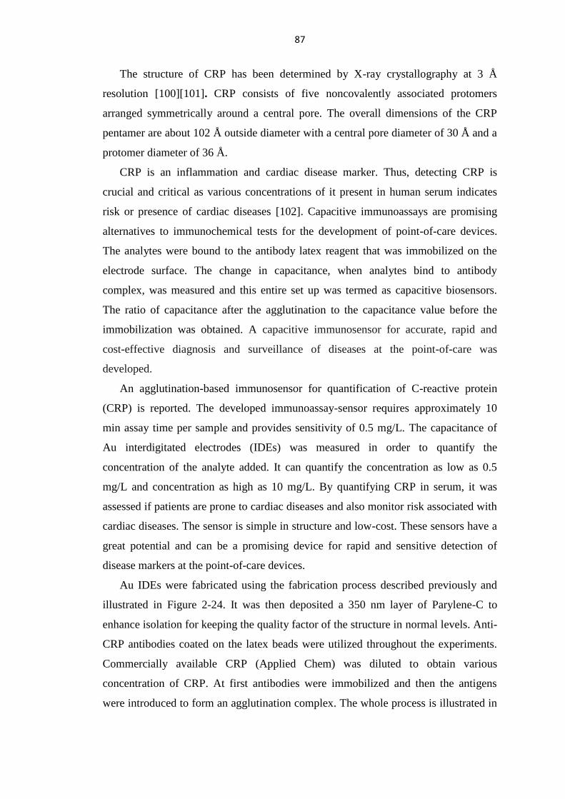
87
The structure of CRP has been determined by X-ray crystallography at 3 Å
resolution [100][101]. CRP consists of five noncovalently associated protomers
arranged symmetrically around a central pore. The overall dimensions of the CRP
pentamer are about 102 Å outside diameter with a central pore diameter of 30 Å and a
protomer diameter of 36 Å.
CRP is an inflammation and cardiac disease marker. Thus, detecting CRP is
crucial and critical as various concentrations of it present in human serum indicates
risk or presence of cardiac diseases [102]. Capacitive immunoassays are promising
alternatives to immunochemical tests for the development of point-of-care devices.
The analytes were bound to the antibody latex reagent that was immobilized on the
electrode surface. The change in capacitance, when analytes bind to antibody
complex, was measured and this entire set up was termed as capacitive biosensors.
The ratio of capacitance after the agglutination to the capacitance value before the
immobilization was obtained. A capacitive immunosensor for accurate, rapid and
cost-effective diagnosis and surveillance of diseases at the point-of-care was
developed.
An agglutination-based immunosensor for quantification of C-reactive protein
(CRP) is reported. The developed immunoassay-sensor requires approximately 10
min assay time per sample and provides sensitivity of 0.5 mg/L. The capacitance of
Au interdigitated electrodes (IDEs) was measured in order to quantify the
concentration of the analyte added. It can quantify the concentration as low as 0.5
mg/L and concentration as high as 10 mg/L. By quantifying CRP in serum, it was
assessed if patients are prone to cardiac diseases and also monitor risk associated with
cardiac diseases. The sensor is simple in structure and low-cost. These sensors have a
great potential and can be a promising device for rapid and sensitive detection of
disease markers at the point-of-care devices.
Au IDEs were fabricated using the fabrication process described previously and
illustrated in Figure 2-24. It was then deposited a 350 nm layer of Parylene-C to
enhance isolation for keeping the quality factor of the structure in normal levels. Anti-
CRP antibodies coated on the latex beads were utilized throughout the experiments.
Commercially available CRP (Applied Chem) was diluted to obtain various
concentration of CRP. At first antibodies were immobilized and then the antigens
were introduced to form an agglutination complex. The whole process is illustrated in
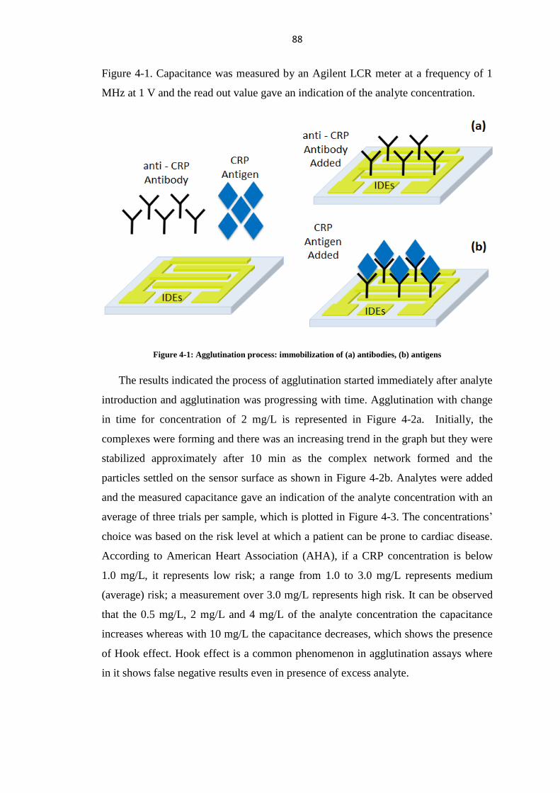
88
Figure 4-1. Capacitance was measured by an Agilent LCR meter at a frequency of 1
MHz at 1 V and the read out value gave an indication of the analyte concentration.
Figure 4-1: Agglutination process: immobilization of (a) antibodies, (b) antigens
The results indicated the process of agglutination started immediately after analyte
introduction and agglutination was progressing with time. Agglutination with change
in time for concentration of 2 mg/L is represented in Figure 4-2a. Initially, the
complexes were forming and there was an increasing trend in the graph but they were
stabilized approximately after 10 min as the complex network formed and the
particles settled on the sensor surface as shown in Figure 4-2b. Analytes were added
and the measured capacitance gave an indication of the analyte concentration with an
average of three trials per sample, which is plotted in Figure 4-3. The concentrations’
choice was based on the risk level at which a patient can be prone to cardiac disease.
According to American Heart Association (AHA), if a CRP concentration is below
1.0 mg/L, it represents low risk; a range from 1.0 to 3.0 mg/L represents medium
(average) risk; a measurement over 3.0 mg/L represents high risk. It can be observed
that the 0.5 mg/L, 2 mg/L and 4 mg/L of the analyte concentration the capacitance
increases whereas with 10 mg/L the capacitance decreases, which shows the presence
of Hook effect. Hook effect is a common phenomenon in agglutination assays where
in it shows false negative results even in presence of excess analyte.

89
Figure 4-2: Agglutination progressing with time compared to the Capacitance vs Time diagram
Figure 4-3: Relative Permittivity vs Antigen concentration
3
3.4
3.8
4.2
4.6
0.5 2 4 10
Rel
ativ
e P
erm
itti
vit
y (
e r)
Antigen concentration (mg/L)

90
4.2 Streptavidin - biotinylated BSA quantification
There is an increasing need to detect new proteins in the present era to identify
different organisms and molecules in diagnostics and environment. As a pilot study a
conjugation of streptavidin and biotinylated-BSA was used as the binding is well
understood. This protein is used as a reference for quantifying unknown proteins,
which are compared to a specific BSA amount. It was selected because it is a label-
free detection method. Label-free detection is convenient, non-tedious and time
saving when compared to label-based detection methods. Enzyme-linked
immunosorbent assay (ELISA) [103] is one of the highly sensitive methods but
requires complex sample preparation and long analysis time. Therefore, a capacitive
sensor was utilized that requires less analysis time. To determine sensitivity of the
sensors a widely studied streptavidin - biotin model system for protein – ligand
interaction was employed. Various concentrations of BSA protein were quantified by
using these sensors.
So far streptavidin and biotinylated BSA have been analyzed using most of
systems like surface plasmon resonance (SPR) [104], quartz crystal microbalance
(QCM) [105], electrochemical impedance spectroscopy (EIS) [106] and
microwave [107] sensing. In this study, streptavidin - biotinylated BSA was used in
capacitive sensors that could further be used to study complex protein interactions.
Gold IDEs on a silicon substrate were used and they were coated with 350 nm of
Parylene C. The protocol for streptavidin immobilization is described in [101]. For
stable and covalent immobilization of streptavidin on oxidized silicon is achieved
using 3-mercaptopropyltrimethoxysilane (MPTMS) and N-hydroxysuccinimide ester
(NHS) as linkers. The cleaned silicon chips were silanized in a 2% solution of
MPTMS in dry toluene for 1 h. The silanized chips were incubated for 2 h with NHS -
streptavidin in 50 mM phosphate buffer (pH 7.4). The unattached streptavidin
molecules were washed with 0.5% Tween 20 in phosphate buffer [108]. Biotinylated -
BSA at various concentrations was used and incubated for 1 h at room temperature
and washed with 0.5% Tween 20 in phosphate buffer to remove any unreacted BSA.
The whole protocol process is illustrated in Figure 4-4.

91
Figure 4-4: Protocol for streptavidin immobilization
To determine specificity, non-specific interaction on sensors was carried out using
C - reactive protein. As it is depicted in Figure 4-5, there is clear evidence that the
capacitance increased only for specific interaction. Thus, it was concluded that the
reaction was specific. The ratio of the capacitance in the final measurement to the first
before the process starts is the indication of this difference. This ratio can be
simplified into the relative permittivity of the streptavidin and biotinylated BSA
interaction film since this is the primary reason for this capacitance difference.
Figure 4-5: Results for Protein specificity
1
2
3
4
Non Specific Specific (BSA)
Rel
ativ
e P
erm
itti
vit
y (
e r)
Specificity
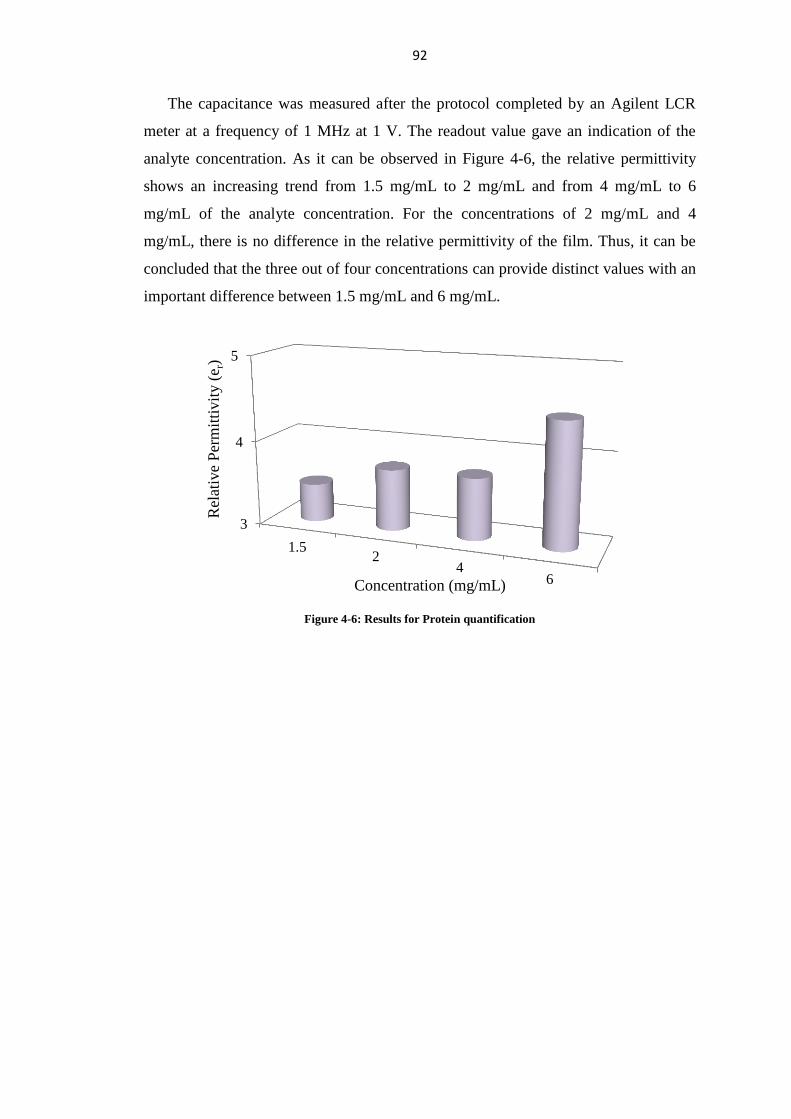
92
The capacitance was measured after the protocol completed by an Agilent LCR
meter at a frequency of 1 MHz at 1 V. The readout value gave an indication of the
analyte concentration. As it can be observed in Figure 4-6, the relative permittivity
shows an increasing trend from 1.5 mg/mL to 2 mg/mL and from 4 mg/mL to 6
mg/mL of the analyte concentration. For the concentrations of 2 mg/mL and 4
mg/mL, there is no difference in the relative permittivity of the film. Thus, it can be
concluded that the three out of four concentrations can provide distinct values with an
important difference between 1.5 mg/mL and 6 mg/mL.
Figure 4-6: Results for Protein quantification
3
4
5
1.52
46
Rel
ativ
e P
erm
itti
vit
y (
e r)
Concentration (mg/mL)

93
Chapter 5: Conclusion and future work
The presented work in this thesis investigates capacitive structures that can
provide high capacitance density, with the IDEs to dominate compared to Fractal
curves (Peano and Hilbert) and Archimedean spiral. The proof of this concept was
conducted through geometrical formula calculations, COMSOL Multiphysics
simulations and cleanroom fabrication on Si substrate with the minimum feature to be
2 um. After this study, it was proven that the Fractals cannot provide the capacitance
density that IDEs achieve, since the fringing capacitance in the corners is less than the
standard capacitance between the bars for specific periphery. Moreover, a low-cost
fabrication process has been conducted on flexible plastic PET with the minimum
feature to be 100 um. In this process, the Hilbert curve has achieved higher
capacitance compared to IDEs, based on fabrication issues (smaller gap size for
Hilbert curve, discontinuities for IDEs).
Moreover, for the gas sensing measuring an automated setup has been
implemented for testing humidity, VOCs vapors and toxic gases effect in the sensors
sensitive film. Custom LabVIEW interfaces provide automation and user-friendly
environment for curves extraction and experiments automation minimizing the
manual effort to the least possible. The system provides reproducible conditions and
results with a wide range of potential sensitive films under test. For this work, the gas
sensing has focused on capacitive sensors by using three different sensing films,
polymers (Nafion, Polyimide) and MOF (Cu(bdc).xH2O). They were tested under
humidity, VOC vapors (Ethanol, Methanol, Acetone, Toluene) and Ammonia.
Polyimide has shown response only in relative humidity testing, which was linear.
Nafion has dominated in sensitivity compared to Cu(bdc).xH2O. Both of them have
shown polynomial responses to relative humidity testing and linear responses to the
VOC vapors and Ammonia. All the sensors have shown reproducible results, recovery
ability and reusability.
As for the biological sensing track, two experiments were conducted based on the
quantification of two proteins, CRP and BSA. CRP is a cardiac disease biomarker and
four different concentrations were attempted to be quantified (0.5 mg/L, 2 mg/L, 4
mg/L and 10 mg/L). The relative permittivity per concentration was distinct and thus
each level was easily differentiated. BSA is a label-free detection method and its
94
quantification provided distinct results for three out of four concentrations (1.5
mg/mL, 2-4 mg/mL (the same response), 6 mg/mL).
Possible extensions of the current work that can enhance its impact are the
following recommended future research points:
Full integration: Since the concept of gas and biological capacitive sensing
has been proved experimentally, the next step can be the full integration of the
sensor and the capacitance to digital converters (CDC) chips for gas and
biological sensing in order to achieve a full functional and miniaturized
system.
Different substrates and fabrication methods: Except the flexible plastic PET,
there are also some other materials as paper, fabric or Kapton that can be used
as substrates for the IDEs. The fabrication process can be either the
aforementioned subtractive method with sputtering and maskless etching, or it
can be extended in inkjet or screen printing, which can avoid the loss of
conductive material.
Gas sensing: Different materials should be employed since each of them
normally gives a different response. Based on this fact, arrays of sensors can
be tested and with the assistance of pattern recognition algorithms, an e-nose
implementation will be possible but it is still a challenging field.
Biological sensing: The quantification of CRP and BSA are indicative and the
focus can be directed in more experiments in this field. Moreover, the
integration in lab-on-chip applications using microfluidics structures can
provide a compact device.

95
Appendix
Data acquisition with automatic curve extraction
The purpose of this vi implementation is to acquire the data from a LCR meter
and a Multimeter and extract automated the curves in Excel files.
LCR (Agilent 4980A)
The LCR meter measures passive components with an error no more than 0.05 %,
if the capacitor or inductor device under test (DUT) does not have a significant
resistive component of impedance. An AC signal with selectable test frequency is
applied to the DUT and the LCR meter applies a voltage over and reads the current
through it. The ratio of those two values will determine the impedance magnitude and
the phase angle, which will show the type of element under test.
There are two basic models that a LCR can assume: a parallel or a series. For high
amplitude of reactance, the parasitic resistance in series is probably negligible, which
will prove a parallel model more accurate and vice versa. Hence, in general, there is a
tendency to use the parallel circuit model for small capacitors and the series model for
large capacitors.
Figure 0-1: Graph for selecting the most accurate model [109]
Except the rule based on Figure 0-1, in general, LR measurements use the series
model, where a parasitic resistance is in series and it can be the resistance of the
inductor coil and CR measurements use the parallel model, where the capacitor is
considered to have a leaky dielectric.

96
In our experiments, the parallel model for capacitive measurements was
employed, since the capacitance of the DUT is in the range of picofarads. The LCR
interface can be observed in Figure 0-2. The LabVIEW library for the Agilent LCR
was utilized. Before the while loop, as shown in Figure 0-3, the LCR meter is
initialized and the type of measurements and the applied signal are set. Moreover, the
LCR is used also as a DC source for the commercial humidity sensor. Hence, the
corresponding function of the library is used for giving the option to the user to select
the level of the output DC signal.
Figure 0-2: LCR control in Front Panel
Figure 0-3: LCR initialization
Figure 0-4: AC and DC applied signal option

97
The user also has the option to select the type of the measurements (AC or DC). If
it is AC, there are four options with frequencies, which can also be omitted with the
Boolean button next to them. If it is DC, there is only one frequency as illustrated in
Figure 0-4, f = 0 Hz, is sent to the LCR but due to the limitations of it, the lowest
frequency of a signal is 20 Hz.
Multimeter (Agilent 34401A)
The digital multimeter is considered one of the most popular equipment for testing
electronics. Its capabilities are including measurements of resistance, voltage and
current for both AC and DC signals.
The digital multimeter was used for the humidity sensing with the front panel
shown in Figure 0-5. A commercial humidity sensor (HIH-4000 Series) was
connected and fed from the LCR meter with 1 V. The output voltage (𝑉𝑜𝑢𝑡) was
measured by the multimeter, as shown in Figure 0-6. This value was
correlated to the relative humidity with the sensors datasheet equation:
𝑅𝐻% =𝑉𝑜𝑢𝑡 − 0.848
0.031
Figure 0-5: Multimeter control in Front panel
Figure 0-6: Multimeter in Block diagram
The LabVIEW library for the Agilent multimeter is employed. At the beginning of
the while loop, the device is initialized, the measurement type and time integration

98
settings are set with giving the option to the user to select the necessary. Inside the
while loop, the value of the multimeter reads voltage per iteration, which value
corresponds to relative humidity (RH%) appearing as indication on the front panel.
The communication with the Multimeter is stopped by a vi when the loop ends.
Curves extraction
The outcome of the experiment is to extract a curve (Capacitance versus RH%),
based on the points with the different concentrations. In order to automatically select
the points when the concentration has stabilized, the user should insert the targeted
Accuracy, which is the difference between the previous and the current value of the
humidity and the number of consecutive points that meet this accuracy. This check is
used in order to avoid points that are not useful for the curves. The average value of
these points is selected, as it is depicted in Figure 0-7, and it is extracted in the final
curve. All these points are saved into matrixes and then they are plotted for each
frequency either as bare points or as curves using Least Square fitting, as shown in
Figure 0-8.
Figure 0-7: LabVIEW code for Accuracy and averaging
Figure 0-8: XY graphs for plotting capacitance vs humidity curves
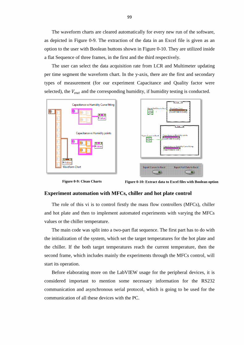
99
The waveform charts are cleared automatically for every new run of the software,
as depicted in Figure 0-9. The extraction of the data in an Excel file is given as an
option to the user with Boolean buttons shown in Figure 0-10. They are utilized inside
a flat Sequence of three frames, in the first and the third respectively.
The user can select the data acquisition rate from LCR and Multimeter updating
per time segment the waveform chart. In the y-axis, there are the first and secondary
types of measurement (for our experiment Capacitance and Quality factor were
selected), the 𝑉𝑜𝑢𝑡 and the corresponding humidity, if humidity testing is conducted.
Figure 0-9: Clean Charts
Figure 0-10: Extract data to Excel files with Boolean option
Experiment automation with MFCs, chiller and hot plate control
The role of this vi is to control firstly the mass flow controllers (MFCs), chiller
and hot plate and then to implement automated experiments with varying the MFCs
values or the chiller temperature.
The main code was split into a two-part flat sequence. The first part has to do with
the initialization of the system, which set the target temperatures for the hot plate and
the chiller. If the both target temperatures reach the current temperature, then the
second frame, which includes mainly the experiments through the MFCs control, will
start its operation.
Before elaborating more on the LabVIEW usage for the peripheral devices, it is
considered important to mention some necessary information for the RS232
communication and asynchronous serial protocol, which is going to be used for the
communication of all these devices with the PC.
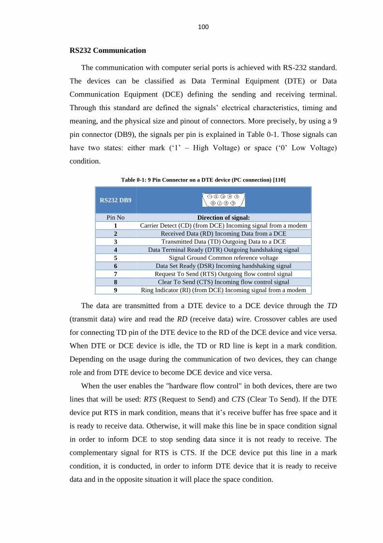
100
RS232 Communication
The communication with computer serial ports is achieved with RS-232 standard.
The devices can be classified as Data Terminal Equipment (DTE) or Data
Communication Equipment (DCE) defining the sending and receiving terminal.
Through this standard are defined the signals’ electrical characteristics, timing and
meaning, and the physical size and pinout of connectors. More precisely, by using a 9
pin connector (DB9), the signals per pin is explained in Table 0-1. Those signals can
have two states: either mark (‘1’ – High Voltage) or space (‘0’ Low Voltage)
condition.
Table 0-1: 9 Pin Connector on a DTE device (PC connection) [110]
RS232 DB9
Pin No Direction of signal:
1 Carrier Detect (CD) (from DCE) Incoming signal from a modem
2 Received Data (RD) Incoming Data from a DCE
3 Transmitted Data (TD) Outgoing Data to a DCE
4 Data Terminal Ready (DTR) Outgoing handshaking signal
5 Signal Ground Common reference voltage
6 Data Set Ready (DSR) Incoming handshaking signal
7 Request To Send (RTS) Outgoing flow control signal
8 Clear To Send (CTS) Incoming flow control signal
9 Ring Indicator (RI) (from DCE) Incoming signal from a modem
The data are transmitted from a DTE device to a DCE device through the TD
(transmit data) wire and read the RD (receive data) wire. Crossover cables are used
for connecting TD pin of the DTE device to the RD of the DCE device and vice versa.
When DTE or DCE device is idle, the TD or RD line is kept in a mark condition.
Depending on the usage during the communication of two devices, they can change
role and from DTE device to become DCE device and vice versa.
When the user enables the "hardware flow control" in both devices, there are two
lines that will be used: RTS (Request to Send) and CTS (Clear To Send). If the DTE
device put RTS in mark condition, means that it’s receive buffer has free space and it
is ready to receive data. Otherwise, it will make this line be in space condition signal
in order to inform DCE to stop sending data since it is not ready to receive. The
complementary signal for RTS is CTS. If the DCE device put this line in a mark
condition, it is conducted, in order to inform DTE device that it is ready to receive
data and in the opposite situation it will place the space condition.
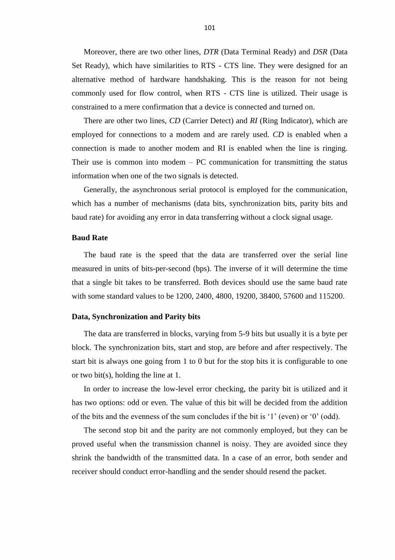
101
Moreover, there are two other lines, DTR (Data Terminal Ready) and DSR (Data
Set Ready), which have similarities to RTS - CTS line. They were designed for an
alternative method of hardware handshaking. This is the reason for not being
commonly used for flow control, when RTS - CTS line is utilized. Their usage is
constrained to a mere confirmation that a device is connected and turned on.
There are other two lines, CD (Carrier Detect) and RI (Ring Indicator), which are
employed for connections to a modem and are rarely used. CD is enabled when a
connection is made to another modem and RI is enabled when the line is ringing.
Their use is common into modem – PC communication for transmitting the status
information when one of the two signals is detected.
Generally, the asynchronous serial protocol is employed for the communication,
which has a number of mechanisms (data bits, synchronization bits, parity bits and
baud rate) for avoiding any error in data transferring without a clock signal usage.
Baud Rate
The baud rate is the speed that the data are transferred over the serial line
measured in units of bits-per-second (bps). The inverse of it will determine the time
that a single bit takes to be transferred. Both devices should use the same baud rate
with some standard values to be 1200, 2400, 4800, 19200, 38400, 57600 and 115200.
Data, Synchronization and Parity bits
The data are transferred in blocks, varying from 5-9 bits but usually it is a byte per
block. The synchronization bits, start and stop, are before and after respectively. The
start bit is always one going from 1 to 0 but for the stop bits it is configurable to one
or two bit(s), holding the line at 1.
In order to increase the low-level error checking, the parity bit is utilized and it
has two options: odd or even. The value of this bit will be decided from the addition
of the bits and the evenness of the sum concludes if the bit is ‘1’ (even) or ‘0’ (odd).
The second stop bit and the parity are not commonly employed, but they can be
proved useful when the transmission channel is noisy. They are avoided since they
shrink the bandwidth of the transmitted data. In a case of an error, both sender and
receiver should conduct error-handling and the sender should resend the packet.
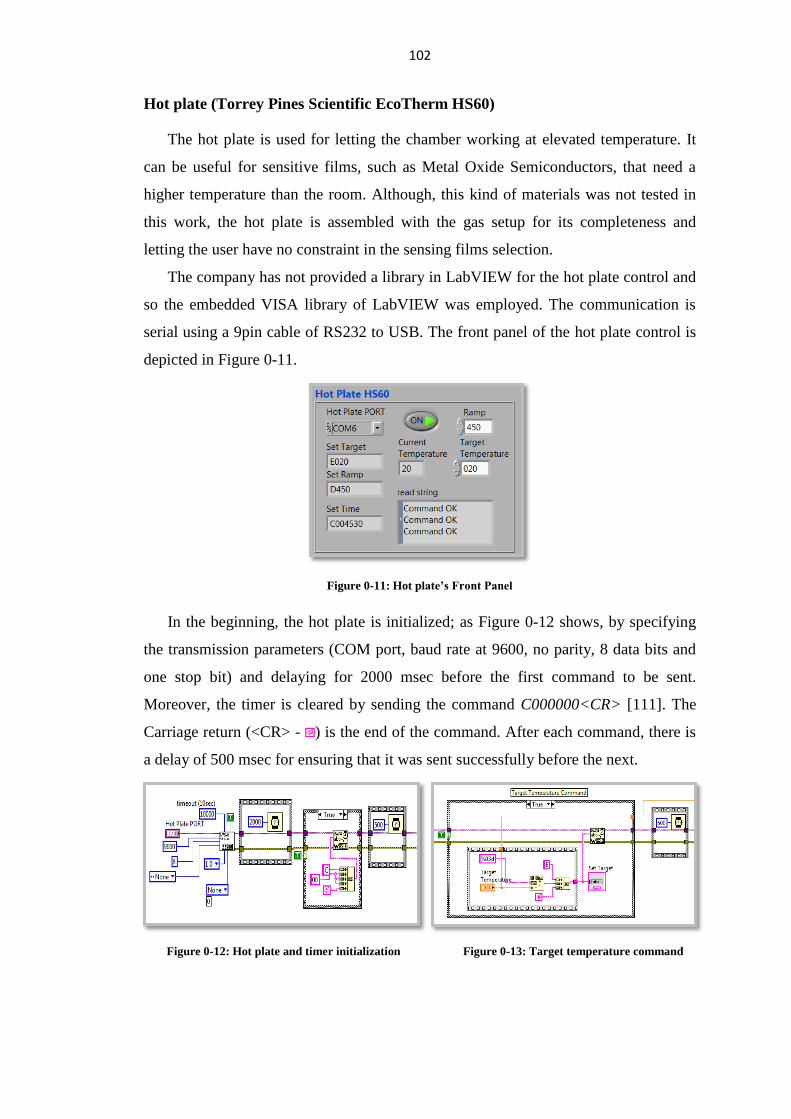
102
Hot plate (Torrey Pines Scientific EcoTherm HS60)
The hot plate is used for letting the chamber working at elevated temperature. It
can be useful for sensitive films, such as Metal Oxide Semiconductors, that need a
higher temperature than the room. Although, this kind of materials was not tested in
this work, the hot plate is assembled with the gas setup for its completeness and
letting the user have no constraint in the sensing films selection.
The company has not provided a library in LabVIEW for the hot plate control and
so the embedded VISA library of LabVIEW was employed. The communication is
serial using a 9pin cable of RS232 to USB. The front panel of the hot plate control is
depicted in Figure 0-11.
Figure 0-11: Hot plate’s Front Panel
In the beginning, the hot plate is initialized; as Figure 0-12 shows, by specifying
the transmission parameters (COM port, baud rate at 9600, no parity, 8 data bits and
one stop bit) and delaying for 2000 msec before the first command to be sent.
Moreover, the timer is cleared by sending the command C000000<CR> [111]. The
Carriage return (<CR> - ) is the end of the command. After each command, there is
a delay of 500 msec for ensuring that it was sent successfully before the next.
Figure 0-12: Hot plate and timer initialization
Figure 0-13: Target temperature command
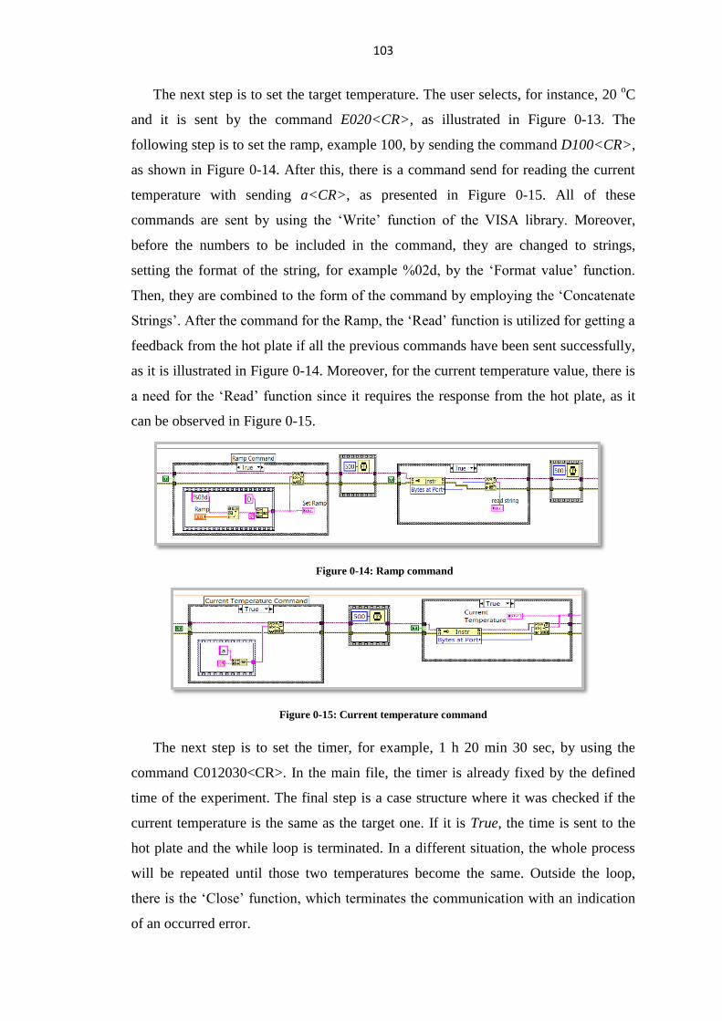
103
The next step is to set the target temperature. The user selects, for instance, 20 oC
and it is sent by the command E020<CR>, as illustrated in Figure 0-13. The
following step is to set the ramp, example 100, by sending the command D100<CR>,
as shown in Figure 0-14. After this, there is a command send for reading the current
temperature with sending a<CR>, as presented in Figure 0-15. All of these
commands are sent by using the ‘Write’ function of the VISA library. Moreover,
before the numbers to be included in the command, they are changed to strings,
setting the format of the string, for example %02d, by the ‘Format value’ function.
Then, they are combined to the form of the command by employing the ‘Concatenate
Strings’. After the command for the Ramp, the ‘Read’ function is utilized for getting a
feedback from the hot plate if all the previous commands have been sent successfully,
as it is illustrated in Figure 0-14. Moreover, for the current temperature value, there is
a need for the ‘Read’ function since it requires the response from the hot plate, as it
can be observed in Figure 0-15.
Figure 0-14: Ramp command
Figure 0-15: Current temperature command
The next step is to set the timer, for example, 1 h 20 min 30 sec, by using the
command C012030<CR>. In the main file, the timer is already fixed by the defined
time of the experiment. The final step is a case structure where it was checked if the
current temperature is the same as the target one. If it is True, the time is sent to the
hot plate and the while loop is terminated. In a different situation, the whole process
will be repeated until those two temperatures become the same. Outside the loop,
there is the ‘Close’ function, which terminates the communication with an indication
of an occurred error.
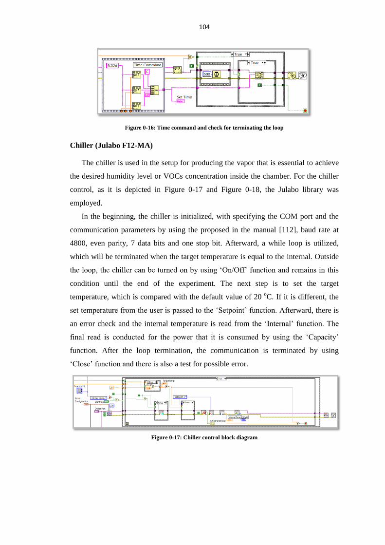
104
Figure 0-16: Time command and check for terminating the loop
Chiller (Julabo F12-MA)
The chiller is used in the setup for producing the vapor that is essential to achieve
the desired humidity level or VOCs concentration inside the chamber. For the chiller
control, as it is depicted in Figure 0-17 and Figure 0-18, the Julabo library was
employed.
In the beginning, the chiller is initialized, with specifying the COM port and the
communication parameters by using the proposed in the manual [112], baud rate at
4800, even parity, 7 data bits and one stop bit. Afterward, a while loop is utilized,
which will be terminated when the target temperature is equal to the internal. Outside
the loop, the chiller can be turned on by using ‘On/Off’ function and remains in this
condition until the end of the experiment. The next step is to set the target
temperature, which is compared with the default value of 20 oC. If it is different, the
set temperature from the user is passed to the ‘Setpoint’ function. Afterward, there is
an error check and the internal temperature is read from the ‘Internal’ function. The
final read is conducted for the power that it is consumed by using the ‘Capacity’
function. After the loop termination, the communication is terminated by using
‘Close’ function and there is also a test for possible error.
Figure 0-17: Chiller control block diagram
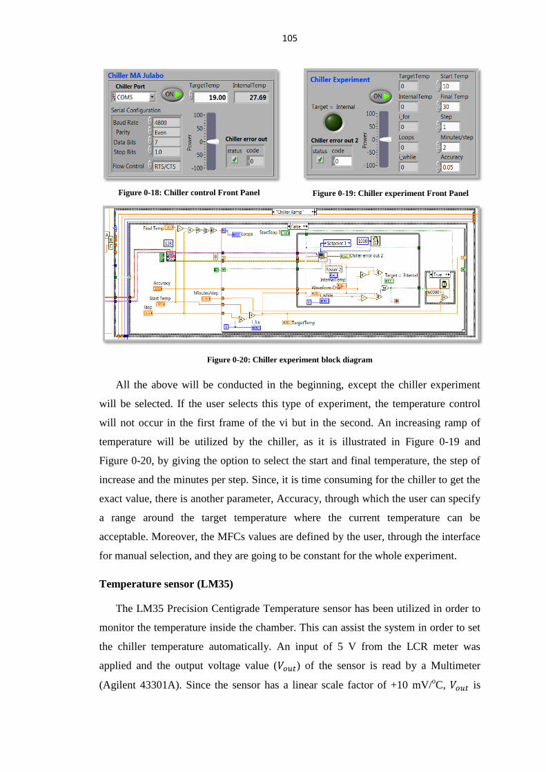
105
Figure 0-18: Chiller control Front Panel
Figure 0-19: Chiller experiment Front Panel
Figure 0-20: Chiller experiment block diagram
All the above will be conducted in the beginning, except the chiller experiment
will be selected. If the user selects this type of experiment, the temperature control
will not occur in the first frame of the vi but in the second. An increasing ramp of
temperature will be utilized by the chiller, as it is illustrated in Figure 0-19 and
Figure 0-20, by giving the option to select the start and final temperature, the step of
increase and the minutes per step. Since, it is time consuming for the chiller to get the
exact value, there is another parameter, Accuracy, through which the user can specify
a range around the target temperature where the current temperature can be
acceptable. Moreover, the MFCs values are defined by the user, through the interface
for manual selection, and they are going to be constant for the whole experiment.
Temperature sensor (LM35)
The LM35 Precision Centigrade Temperature sensor has been utilized in order to
monitor the temperature inside the chamber. This can assist the system in order to set
the chiller temperature automatically. An input of 5 V from the LCR meter was
applied and the output voltage value (𝑉𝑜𝑢𝑡) of the sensor is read by a Multimeter
(Agilent 43301A). Since the sensor has a linear scale factor of +10 mV/oC, 𝑉𝑜𝑢𝑡 is
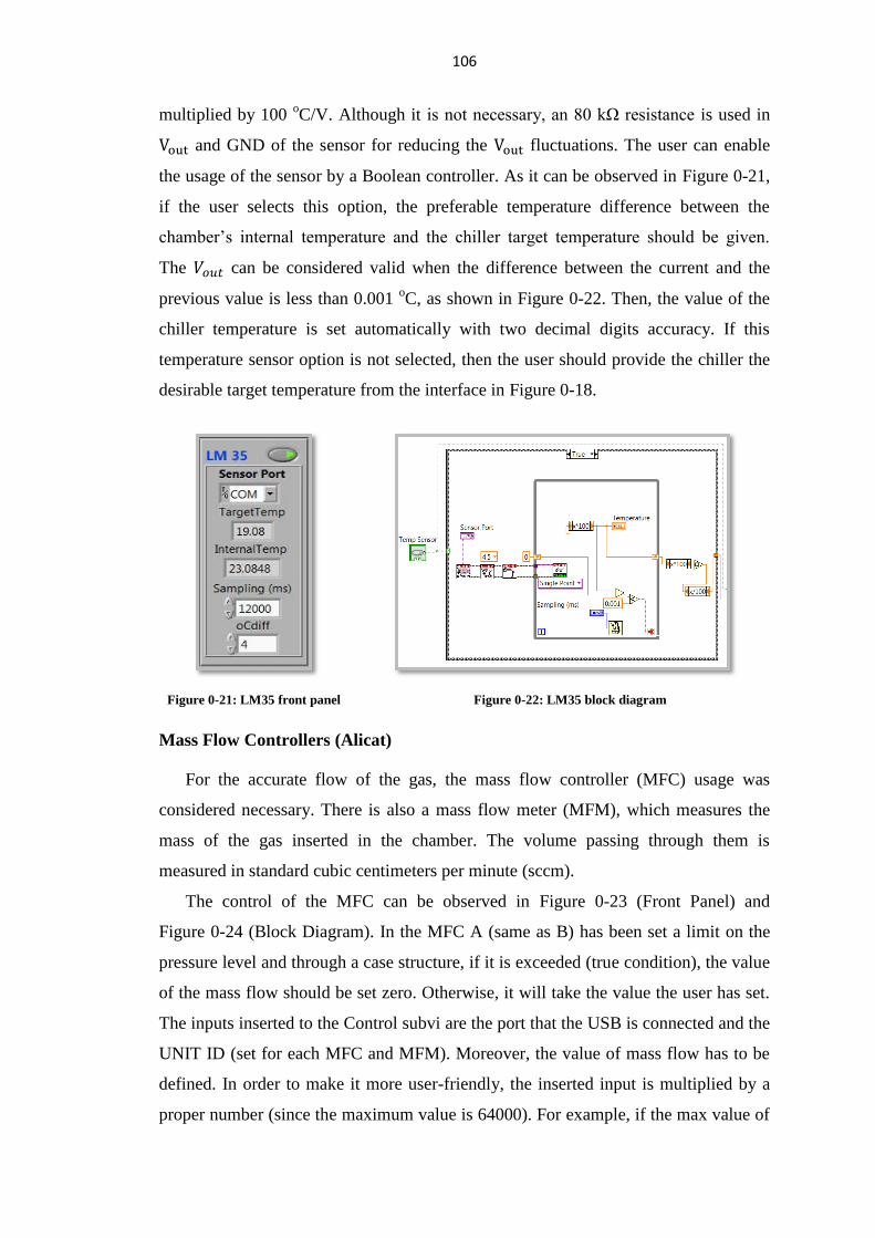
106
multiplied by 100 oC/V. Although it is not necessary, an 80 kΩ resistance is used in
Vout and GND of the sensor for reducing the Vout fluctuations. The user can enable
the usage of the sensor by a Boolean controller. As it can be observed in Figure 0-21,
if the user selects this option, the preferable temperature difference between the
chamber’s internal temperature and the chiller target temperature should be given.
The 𝑉𝑜𝑢𝑡 can be considered valid when the difference between the current and the
previous value is less than 0.001 oC, as shown in Figure 0-22. Then, the value of the
chiller temperature is set automatically with two decimal digits accuracy. If this
temperature sensor option is not selected, then the user should provide the chiller the
desirable target temperature from the interface in Figure 0-18.
Mass Flow Controllers (Alicat)
For the accurate flow of the gas, the mass flow controller (MFC) usage was
considered necessary. There is also a mass flow meter (MFM), which measures the
mass of the gas inserted in the chamber. The volume passing through them is
measured in standard cubic centimeters per minute (sccm).
The control of the MFC can be observed in Figure 0-23 (Front Panel) and
Figure 0-24 (Block Diagram). In the MFC A (same as B) has been set a limit on the
pressure level and through a case structure, if it is exceeded (true condition), the value
of the mass flow should be set zero. Otherwise, it will take the value the user has set.
The inputs inserted to the Control subvi are the port that the USB is connected and the
UNIT ID (set for each MFC and MFM). Moreover, the value of mass flow has to be
defined. In order to make it more user-friendly, the inserted input is multiplied by a
proper number (since the maximum value is 64000). For example, if the max value of
Figure 0-21: LM35 front panel
Figure 0-22: LM35 block diagram
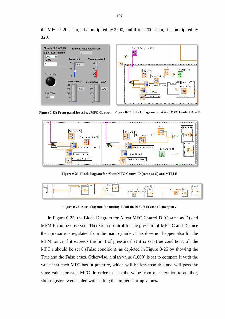
107
the MFC is 20 sccm, it is multiplied by 3200, and if it is 200 sccm, it is multiplied by
320.
Figure 0-23: Front panel for Alicat MFC Control
Figure 0-24: Block diagram for Alicat MFC Control A & B
Figure 0-25: Block diagram for Alicat MFC Control D (same as C) and MFM E
Figure 0-26: Block diagram for turning off all the MFC’s in case of emergency
In Figure 0-25, the Block Diagram for Alicat MFC Control D (C same as D) and
MFM E can be observed. There is no control for the pressure of MFC C and D since
their pressure is regulated from the main cylinder. This does not happen also for the
MFM, since if it exceeds the limit of pressure that it is set (true condition), all the
MFC’s should be set 0 (False condition), as depicted in Figure 0-26 by showing the
True and the False cases. Otherwise, a high value (1000) is set to compare it with the
value that each MFC has in pressure, which will be less than this and will pass the
same value for each MFC. In order to pass the value from one iteration to another,
shift registers were added with setting the proper starting values.

108
The MFC shows the absolute pressure and includes the atmospheric by using
pounds per square inch absolute (PSIA). So, this value should be inserted in the limit
controller. If gage pressure (PSIG) is selected, the subtraction of local atmospheric
pressure from the absolute pressure reading should be inserted: PSIG = PSIA – (Local
Atmospheric Pressure) [113].
Figure 0-27: Front panel for MFC Control subvi
Figure 0-28: Block diagram for MFC Control subvi
A subvi is implemented for controlling the mass flow that passes through the
MFC and returns the Pressure, Temperature, Volumetric and Mass Flow, as it can be
observed in Figure 0-27 and Figure 0-28 in the Front Panel and the Block Diagram
respectively [114]. A Stacked Sequence Structure is used in order first to read the
condition of the MFC, then to insert the level of the mass flow that will be allowed to
pass and finally it will be read again to give the final condition. Alicat’s Labview
library is employed for Reading and Writing to the MFC. The communication is
Serial RS-232TX through a Multi-drop Breakout Box (BB9), in which all the MFC’s
are connected for transferring data and power.
Experiment Automation
All the above automation per instrument has been conducted for controlling the
parts of the setup and being used in prearranged experiments for achieving a friendlier
user environment. Different kinds of tests are needed for verifying the results.
The main experiments were purge (Figure 0-29a) and ramp (Figure 0-29b) for all
the gases (water vapor, VOCs vapor and toxic). Moreover, there is an option for the
reverse experiment, depicted in Figure 0-29c. Those responses are under the testing of

109
the commercial sensor. In each case, the corresponding MFC is used under specific
sccm values. An additional experiment that it was mentioned before is the chiller
ramp. If none of the above experiments satisfy the user needs, there is an option for
manual control the value of MFCs. The user selects the necessary experiment, inserts
the time per step of the experiment and the remaining time appears by running the vi.
All of these features appear in Figure 0-30.
Figure 0-29: (a) Purge, (b) Ramp and (c) Reverse experiment of HIH-4000
Figure 0-30: Front panel for experiments option, remaining experiment time and manual selection
By the time the user selects the desired experiment, the overall time is calculated
by number of steps for each experiment. For the For Loop, where the whole process is
enfolded, the number of iterations is specified by the overall time. Each minute needs
24 loops and thus the minutes are multiplied with this number, as shown in
Figure 0-31. The next step is to deduct from the starting time the seconds that have
been elapsed per iteration. The whole process is illustrated in Figure 0-32.

110
Figure 0-31: Number of iterations based on the minutes per step
Figure 0-32: Remaining time calculation
All the experiments were included in subvi’s and inserted into a case structure, as
shown in Figure 0-33, which was controlled by an Enum (multiple enumerated cases).
If the step in the experiment was not changed, the values of the MFCs were repeated
per iteration. The subvi of each experiment is depicted in Figure 0-34, where each
step is in folded case structures.
Figure 0-33: Case structure for the experiments
Figure 0-34: Subvi implementation with folded case structures (False conditions)

111
References
[1] Liu, Xiao, et al. "A survey on gas sensing technology." Sensors 12.7 (2012): 9635-9665.
[2] Peris, Miguel, and Laura Escuder-Gilabert. "A 21st century technique for food control: Electronic
noses." Analytica Chimica Acta 638.1 (2009): 1-15.
[3] Righettoni, Marco, Antonio Tricoli, and Sotiris E. Pratsinis. "Si: WO3 sensors for highly selective
detection of acetone for easy diagnosis of diabetes by breath analysis." Analytical chemistry 82.9
(2010): 3581-3587.
[4] Oh, Eun Hae, Hyun Seok Song, and Tai Hyun Park. "Recent advances in electronic and
bioelectronic noses and their biomedical applications." Enzyme and microbial technology 48.6
(2011): 427-437.
[5] Grieshaber, Dorothee, et al. "Electrochemical biosensors-sensor principles and architectures."
Sensors 8.3 (2008): 1400-1458.
[6] http://www.pwc.com/us/en/technology-forecast/2013/issue1/features/technology-guide-customers-
toward-goals.jhtml
[7] Latest Market Research Report in Global Gas Sensors Market, , Grand View Research Inc.
[8] Gas Sensors Market - Global Industry Size, Share, Trends, Analysis and Forecast 2012 – 2018,
Transparency market research
[9] Gas Sensors Market Analysis And Segment Forecasts To 2020, Grand View Research Inc.
[10] Elshurafa, Amro M., et al. "RF MEMS fractal capacitors with high self-resonant frequencies."
Microelectromechanical Systems, Journal of 21.1 (2012): 10-12.
[11] Mandelbrot, Benoit. Fractals and chaos: the Mandelbrot set and beyond. Vol. 3. Springer, 2004.
[12] Sagan, Hans. Space-filling curves. Vol. 18. New York: Springer-Verlag, 1994.
[13] H. Omran, “Low-Power Integrated Capacitive Sensing Microsystems”, PhD Proposal, 2013.
[14] L. E. Kreno, K. Leong, O. K. Farha, M. Allendorf, R. P. Van Duyne, and J. T. Hupp, “Metal-
organic framework materials as chemical sensors,” Chemical Reviews, vol. 112, no. 2, pp. 1105–
1125, 2012.
[15] AZ 1500 Photoresist, Data Package, AZ Electronic Materials
[16] http://www.goodfellow.com/A/Polyethylene-terephthalate.html
[17] Amin, Yasar, et al. "Performance-optimized quadrate bowtie RFID antennas for cost-effective and
eco-friendly industrial applications." Progress In Electromagnetics Research 126 (2012): 49-64.
[18] Altenberend, U., et al. "Towards fully printed capacitive gas sensors on flexible PET substrates
based on Ag interdigitated transducers with increased stability." Sensors and Actuators B:
Chemical 187 (2013): 280-287.
[19] Molina-Lopez, F. et al. "Large arrays of inkjet-printed MEMS microbridges on foil." Micro
Electro Mechanical Systems (MEMS), 2014 IEEE 27th International Conference on. IEEE, 2014.
[20] Claramunt, S., et al. "Flexible gas sensor array with an embedded heater based on metal decorated
carbon nanofibres." Sensors and Actuators B: Chemical 187 (2013): 401-406.
[21] Kim, Yong Shin, et al. "Gas sensor measurement system capable of sampling volatile organic
compounds (VOCs) in wide concentration range." Sensors and Actuators B: Chemical 122.1

112
(2007): 211-218.
[22] Araki, Hideo, and Sigeru Omatu. "Measurement system for metal-oxide gas sensors." Artificial
Life and Robotics 17.3-4 (2013): 357-361.
[23] Heinemeyer, Andreas, Verena Gruber, and Michael Bahn. "The ‘Gas-Snake’: Design and
validation of a versatile membrane-based gas flux measurement system in a grassland soil
respiration study." Agricultural and Forest Meteorology 154 (2012): 166-173.
[24] Pignanelli, Eliseo, K. Kuhn, and A. Schutze. "Versatile gas measurement system based on
combined NDIR transmission and photoacoustic spectroscopy." Sensors, 2011 IEEE. IEEE, 2011.
[25] Pawar, R. C., et al. "Growth of ZnO nanodisk, nanospindles and nanoflowers for gas sensor: pH
dependency." Current Applied Physics 12.3 (2012): 778-783.
[26] Gupta, S. K., Aditee Joshi, and Manmeet Kaur. "Development of gas sensors using ZnO
nanostructures." Journal of Chemical Sciences 122.1 (2010): 57-62.
[27] Chen, Hao, et al. "A comparative study on UV light activated porous TiO2 and ZnO film sensors
for gas sensing at room temperature." Ceramics International 38.1 (2012): 503-509.
[28] Righettoni, Marco, et al. "Breath acetone monitoring by portable Si: WO3 gas sensors." Analytica
chimica acta 738 (2012): 69-75.
[29] http://www.rsc.org/chemistryworld/Issues/2003/January/breath.asp
[30] Wang, X.; Li, Qunqing; Xie, Jing; Jin, Zhong; Wang, Jinyong; Li, Yan; Jiang, Kaili; Fan,
Shoushan (2009). "Fabrication of Ultralong and Electrically Uniform Single-Walled Carbon
Nanotubes on Clean Substrates". Nano Letters 9 (9): 3137–3141.
[31] Llobet, Eduard. "Gas sensors using carbon nanomaterials: A review." Sensors and Actuators B:
Chemical 179 (2013): 32-45.
[32] Thai, T.T.; Yang, L.; DeJean, G.R.; Tentzeris, M.M. Nanotechnology enables wireless gas sensing.
IEEE Microw. Mag. 2011, 12, 84–95.
[33] Star, Alexander, et al. "Gas sensor array based on metal-decorated carbon nanotubes." The Journal
of Physical Chemistry B 110.42 (2006): 21014-21020.
[34] Zilberman, Y., Ionescu, R., Feng, X., Mullen, K., & Haick, H. (2011). Nanoarray of polycyclic
aromatic hydrocarbons and carbon nanotubes for accurate and predictive detection in real-world
environmental humidity. ACS nano, 5(8), 6743-6753.
[35] Jang, Jyongsik, and Joonwon Bae. "Carbon nanofiber/polypyrrole nanocable as toxic gas sensor."
Sensors and Actuators B: Chemical 122.1 (2007): 7-13.
[36] Lee, Jun Seop, et al. "WO3 nanonodule-decorated hybrid carbon nanofibers for NO 2 gas sensor
application." Journal of Materials Chemistry A 1.32 (2013): 9099-9106.
[37] Novoselov, Kostya S., et al. "Electric field effect in atomically thin carbon films." science
306.5696 (2004): 666-669.
[38] F. Schedin, A.K. Geim, S.V. Morozov, E.W. Hill, P. Blake, M.I. Katsnelson, K.S Novoselov,
Detection of individual gas molecules adsorbed on graphene, Nature Materials 6 (2007) 652–655.
[39] J. Dai, J. Yuan, P. Gianozzi, Gas adsorption on graphene doped with B, N, Al, and S: a theoretical
study, Applied Physics Letters 95 (2009) 232105.
113
[40] Ko, G., Kim, H. Y., Ahn, J., Park, Y. M., Lee, K. Y., & Kim, J. (2010). Graphene-based nitrogen
dioxide gas sensors. Current Applied Physics, 10(4), 1002-1004.
[41] Zhang, Zhenyu, et al. "Highly aligned SnO2 nanorods on graphene sheets for gas sensors." Journal
of Materials Chemistry 21.43 (2011): 17360-17365.
[42] Shekhah, O., et al. " MOF thin films: existing and future applications." Chemical Society Reviews
40.2 (2011): 1081-1106.
[43] Kreno, Lauren E., et al. "Metal–organic framework materials as chemical sensors." Chemical
reviews 112.2 (2011): 1105-1125.
[44] B. Zhang, R. Fu, M. Zhang, X. Dong, L. Wang, C.U. Pittman, Gas sensitive vapor grown carbon
nanofiber/polystyrene sensors, Materials Research Bulletin 41 (2006) 553–562.
[45] Achmann, Sabine, et al. "Metal-organic frameworks for sensing applications in the gas phase."
Sensors 9.3 (2009): 1574-1589.
[46] Barea, Elisa, Carmen Montoro, and Jorge AR Navarro. "Toxic gas removal–metal–organic
frameworks for the capture and degradation of toxic gases and vapours." Chem. Soc. Rev. (2014).
[47] Lu, Guang, and Joseph T. Hupp. "Metal− organic frameworks as sensors: a ZIF-8 based Fabry−
Pérot device as a selective sensor for chemical vapors and gases." Journal of the American
Chemical Society 132.23 (2010): 7832-7833.
[48] Traversa, E. Ceramic sensors for humidity detection: the state-of-the-art and future development.
Sens. Actuat. B: Chem. 1995, 23, 135-156.
[49] Bai, Hua, and Gaoquan Shi. "Gas sensors based on conducting polymers." Sensors 7.3 (2007):
267-307.
[50] Cho, Jae-Hyun, et al. "Sensing behaviors of polypyrrole sensor under humidity condition." Sensors
and Actuators B: Chemical 108.1 (2005): 389-392.
[51] Konvalina, Gady, and Hossam Haick. "Sensors for breath testing: from nanomaterials to
comprehensive disease detection." Accounts of chemical research 47.1 (2013): 66-76.
[52] Sanchez, Juan M., and Richard D. Sacks. "GC analysis of human breath with a series-coupled
column ensemble and a multibed sorption trap." Analytical chemistry 75.10 (2003): 2231-2236.
[53] Schwarz, K., W. Filipiak, and A. Amann. "Determining concentration patterns of volatile
compounds in exhaled breath by PTR-MS." Journal of Breath Research 3.2 (2009): 027002.
[54] Smith, David, and Patrik Španěl. "Selected ion flow tube mass spectrometry (SIFT‐MS) for on‐line
trace gas analysis." Mass Spectrometry Reviews 24.5 (2005): 661-700.
[55] Shnayderman, Marianna, et al. "Species-specific bacteria identification using differential mobility
spectrometry and bioinformatics pattern recognition." Analytical chemistry 77.18 (2005): 5930-
5937.
[56] Righettoni, M., et al. "Correlations between blood glucose and breath components from portable
gas sensors and PTR-TOF-MS." Journal of breath research 7.3 (2013): 037110.
[57] Fleischer, Maximilian, et al. "Detection of volatile compounds correlated to human diseases
through breath analysis with chemical sensors." Sensors and Actuators B: Chemical 83.1 (2002):
245-249.

114
[58] Peng, Gang, et al. "Diagnosing lung cancer in exhaled breath using gold nanoparticles." Nature
Nanotechnology 4.10 (2009): 669-673.
[59] Di Natale, Corrado, et al. "Lung cancer identification by the analysis of breath by means of an
array of non-selective gas sensors." Biosensors and Bioelectronics 18.10 (2003): 1209-1218.
[60] Comini, E., et al. "Stable and highly sensitive gas sensors based on semiconducting oxide
nanobelts." Applied Physics Letters 81.10 (2002): 1869-1871.
[61] Shin, Jungwoo, et al. "Thin‐Wall Assembled SnO2 Fibers Functionalized by Catalytic Pt
Nanoparticles and their Superior Exhaled‐Breath‐Sensing Properties for the Diagnosis of
Diabetes." Advanced Functional Materials 23.19 (2013): 2357-2367.
[62] http://www.sensirion.com/en/technology/humidity/
[63] http://www.micronas.com/en/products/gas-sensors
[64] Shibata, Hideo, et al. "A digital hygrometer using a polyimide film relative humidity sensor."
Instrumentation and Measurement, IEEE Transactions on 45.2 (1996): 564-569.
[65] Paşahan, Aziz. "Sensor Applications of Polyimides.", INTECH Open Access Publisher (2012).
[66] Mauritz, Kenneth A., and Robert B. Moore. "State of understanding of Nafion."Chemical
reviews 104.10 (2004): 4535-4586.
[67] Perma Pure LLC (2006). “Nafion physical properties.” Technical Notes and Articles.
[68] Heitner-Wirguin, Carla. "Recent advances in perfluorinated ionomer membranes: structure,
properties and applications." Journal of Membrane Science 120.1 (1996): 1-33.
[69] Ablat, Hayrensa, et al. "Nafion film/K+-exchanged glass optical waveguide sensor for BTX
detection." Analytical chemistry 80.20 (2008): 7678-7683.
[70] Raimundo Jr, IvoáM. "Evaluation of Nafion–Crystal Violet films for the construction of an optical
relative humidity sensor." Analyst 124.11 (1999): 1623-1627.
[71] Sadaoka, Yoshihiko, et al. "Optical humidity sensing characteristics of Nafion—dyes composite
thin films." Sensors and Actuators B: Chemical 7.1 (1992): 443-446.
[72] Mercado, R. C., and F. Moussy. "In vitro and in vivo mineralization of Nafion membrane used for
implantable glucose sensors." Biosensors and Bioelectronics 13.2 (1998): 133-145.
[73] Chen, Hui-Wen, et al. "The application of CNT/Nafion composite material to low humidity
sensing measurement." Sensors and Actuators B: Chemical 104.1 (2005): 80-84.
[74] Su, Pi-Guey, Yi-Lu Sun, and Chu-Chieh Lin. "A low humidity sensor made of quartz crystal
microbalance coated with multi-walled carbon nanotubes/Nafion composite material films."
Sensors and Actuators B: Chemical 115.1 (2006): 338-343.
[75] Wu, Ren-Jang, et al. "Composite of TiO2 nanowires and Nafion as humidity sensor material."
Sensors and Actuators B: Chemical 115.1 (2006): 198-204.
[76] Arslan, Hasan K., et al. "Intercalation in Layered Metal–Organic Frameworks: Reversible
Inclusion of an Extended π-System." Journal of the American Chemical Society 133.21 (2011):
8158-8161.
[77] Hersee, S. D., and J. M. Ballingall. "The operation of metalorganic bubblers at reduced pressure."
Journal of Vacuum Science & Technology A 8.2 (1990): 800-804.

115
[78] Yao, Wei, Xuejiao Chen, and Jian Zhang. "A capacitive humidity sensor based on gold–PVA
core–shell nanocomposites." Sensors and Actuators B: Chemical 145.1 (2010): 327-333.
[79] Wang, Yun, et al. "A capacitive humidity sensor based on ordered macroporous silicon with thin
film surface coating." Sensors and Actuators B: Chemical 149.1 (2010): 136-142.
[80] Zhao, Cheng-Long, Ming Qin, and Qing-An Huang. "A fully packaged CMOS interdigital
capacitive humidity sensor with polysilicon heaters." Sensors Journal, IEEE 11.11 (2011): 2986-
2992.
[81] Wang, Hai Yan, et al. "Capacitive humidity sensing properties of SiC nanowires grown on silicon
nanoporous pillar array." Sensors and Actuators B: Chemical166 (2012): 451-456.
[82] Chen, Hui-Juan, et al. "Capacitive humidity sensor based on amorphous carbon film/n-Si
heterojunctions." Sensors and Actuators B: Chemical 150.1 (2010): 487-489.
[83] Kim, Ji-Hong, et al. "High-performance capacitive humidity sensor with novel electrode and
polyimide layer based on MEMS technology." Microsystem technologies 16.12 (2010): 2017-
2021.
[84] Chen, Xuejiao, et al. "Humidity sensing behavior of silicon nanowires with hexamethyldisilazane
modification." Sensors and Actuators B: Chemical 156.2 (2011): 631-636.
[85] Mohanty, Saraju P., and Elias Kougianos. "Biosensors: a tutorial review." Potentials, IEEE 25.2
(2006): 35-40.
[86] Grieshaber, Dorothee, et al. "Electrochemical biosensors-sensor principles and architectures."
Sensors 8.3 (2008): 1400-1458.
[87] Vargas-Bernal, Rafael, Esmeralda Rodríguez-Miranda, and Gabriel Herrera-Pérez. Evolution and
Expectations of Enzymatic Biosensors for Pesticides. INTECH Open Access Publisher, 2012.
[88] Yang, Y.N., Lin, H.I., Wang, J.H., Shiesh, S.C., Lee, G.B., 2009. Biosens. Bioelectron. 24 (10),
3091–3096.
[89] Okuno, J., Maehashi, K., Kerman, K., Takamura, Y., Matsumoto, K., Tamiya, E., 2007. Biosens.
Bioelectron. 22 (9–10), 2377–2381.
[90] Wang, J., Cao, Y., Xu, Y., Li, G., 2009. Biosens. Bioelectron. 25 (2), 532–536.
[91] Ekins, Roger. "Immunoassay: recent developments and future directions." Nuclear medicine and
biology 21.3 (1994): 495-521.
[92] Sia S. K et al 2004. An Integrated Approach to a Portable and Low-Cost Immunoassay for
Resource-Poor Settings. Angew. Chem. Int. Ed. 43, 498
[93] Hatch, Anson, et al. "A rapid diffusion immunoassay in a T-sensor." Nature biotechnology 19.5
(2001): 461-465.
[94] Cho J.H et al 2006. Plastic ELISA-on-a-Chip Based on Sequential Cross-Flow Chromatography.
Anal. Chem. 78, 793
[95] Dodge A et al. 2001. Electrokinetically Driven Microfluidic Chips with Surface-Modified
Chambers for Heterogeneous Immunoassays. Anal. Chem., 73, 3400-3409
[96] Sato K. 2001. Determination of Carcinoembryonic Antigen in Human Sera by Integrated Bead-
Bed Immunoasay in a Microchip for Cancer Diagnosis. Anal. Chem., 73 (6), pp 1213–1218
[97] Gao Y et al. 2005. Development of a novel electrokinetically driven microfluidic immunoassay for
the detection of Helicobacter pylori. Anal. Chim. Acta. 543, 109–116.
[98] Black, Steven, Irving Kushner, and David Samols. "C-reactive protein." Journal of Biological
Chemistry 279.47 (2004): 48487-48490.
116
[99] Du Clos, Terry W., and Carolyn Mold. "C-reactive protein." Immunologic research 30.3 (2004):
261-277.
[100] Shrive, Annette K., et al. "Three dimensional structure of human C-reactive protein." Nature
Structural & Molecular Biology 3.4 (1996): 346-354.
[101] Thompson, Darren, Mark B. Pepys, and Steve P. Wood. "The physiological structure of
human C-reactive protein and its complex with phosphocholine." Structure 7.2 (1999): 169-177.
[102] W.B. Lee, Y.H. Chen, H.I. Lin, S.C. Shiesh, G.B. Lee, Sensors and Actuators B 157 (2011)
710– 721
[103] Engvall, Eva, and Peter Perlmann. "Enzyme-linked immunosorbent assay (ELISA)
quantitative assay of immunoglobulin G." Immunochemistry 8.9 (1971): 871-874.
[104] Homola, Jiri. "Surface plasmon resonance sensors for detection of chemical and biological
species." Chemical reviews 108.2 (2008): 462-493.
[105] Mao, Xiaole, et al. "A nanoparticle amplification based quartz crystal microbalance DNA
sensor for detection of Escherichia coli O157: H7." Biosensors and Bioelectronics 21.7 (2006):
1178-1185.
[106] Pei, Renjun, et al. "Amplification of antigen–antibody interactions based on biotin labeled
protein–streptavidin network complex using impedance spectroscopy." Biosensors and
Bioelectronics 16.6 (2001): 355-361.
[107] Salazar-Alvarez, Marcela, et al. "Label free detection of specific protein binding using a
microwave sensor." Analyst 139.21 (2014): 5335-5338.
[108] Kossek, S., C. Padeste, and L. Tiefenauer. "Immobilization of streptavidin for immunosensors
on nanostructured surfaces." Journal of Molecular Recognition 9.56 (1996): 485-487.
[109] https://bkprecision.desk.com/customer/portal/articles/1535313-how-to-use-a-lcr-meter
[110] http://www.taltech.com/datacollection/articles/serial_intro
[111] Serial Interface Specification for HS-60 Series Hotplates, Revision B, Torrey Pines Scientific.
[112] Operating Manual for Refrigerated and Heating Circulators, 1.951.0366-V2, JULABO GmbH
[113] Operating Manual, Alicat Scientific, 09/18/2013 Rev.29
[114] http://forums.ni.com/t5/Instrument-Control-GPIB-Serial/Control-Alicat-mass-flow-
controllers-MC-series-withLabveiw/td-p/930128