TMS320C6000 DSP Inter-Integrated Circuit (I2C) Module Reference ...
16 CAN Newsletter 3/2021
Analog Devices (AD) provides printed circuit boards (PCB) and components for development of CAN FD based applications. This article shows details and evaluation of a CAN FD circuit board.
CAN FD circuit board reference design
CN-0401 circuit evaluation board (EVAL-ADM3055E-ARDZ) is an Arduino Uno compatible isolated CAN FD
communications port. It offers a possibility to add CAN FD communication to new and existing designs. The described evaluation procedure of the CN-0401 is performed using the Arduino-based development board (EVAL-ADICUP3029).
Circuit function
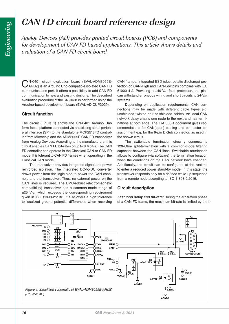
The circuit (Figure 1) shows the CN-0401 Arduino Uno form-factor platform connected via an existing serial periph-eral interface (SPI) to the standalone MCP2518FD control-ler from Microchip and the ADM3055E CAN FD transceiver from Analog Devices. According to the manufacturers, this circuit enables CAN FD bit-rates of up to 8 Mbit/s. The CAN FD controller can operate in the Classical CAN or CAN FD mode. It is tolerant to CAN FD frames when operating in the Classical CAN mode.
The transceiver provides integrated signal and power reinforced isolation. The integrated DC-to-DC converter draws power from the logic side to power the CAN chan-nels and the transceiver. Thus, no external power on the CAN lines is required. The EMC-robust (electromagnetic compatibility) transceiver has a common-mode range of ±25 VDC, which exceeds the corresponding requirement given in ISO 11898-2:2016. It also offers a high tolerance to localized ground potential differences when receiving
CAN frames. Integrated ESD (electrostatic discharge) pro-tection on CAN-High and CAN-Low pins complies with IEC 61000-4-2. Providing a ±40-VDC fault protection, the pins can withstand erroneous wiring and short circuits to 24-VDC systems.
Depending on application requirements, CAN con-nections may be made with different cable types e.g. unshielded twisted-pair or shielded cables. An ideal CAN network daisy chains one node to the next and has termi-nations at both ends. The CiA 303-1 document gives rec-ommendations for CAN(open) cabling and connector pin assignment e.g. for the 9-pin D-Sub connector, as used in the shown circuit.
The switchable termination circuitry connects a 120-Ohm split-termination with a common-mode filtering capacitor between the CAN lines. Switchable termination allows to configure (via software) the termination location when the conditions on the CAN network have changed. Additionally, the circuit can be configured at the runtime to enter a reduced power stand-by mode. In this state, the transceiver responds only on a defined wake-up sequence from a remote node according to ISO 11898-2:2016.
Circuit description
Fast loop delay and bit-rate: During the arbitration phase of a CAN FD frame, the maximum bit-rate is limited by the
Figure 1: Simplified schematic of EVAL-ADM3055E-ARDZ (Source: AD)
5V
D10D9D8D7
2468
1357
P2
P6 P20
P7
SCLKMISOMOSI
D13D12D11
D2
ARDUINO
SCKSDO
CS
VDDU2
MCP2518 U1ADM3055E
SDIINT
TXD
R2160.4Ω
K1AQY221RV
K2AQY221RV
VCC
RXDSTBYAUXIN
SILENT
GND1
TXCANRXCAN
RS
GND2
AGND2
AGND2
AGND2
AGND2
AGND2
AUXOUT
INT0INT1
D4
AGND1
P5
123
321
P19123
GND
CANLCANH
P4
P1
DB9CONNECTOR
123
R2260.4Ω
R203.48kΩ
C94700pFR5
47kΩ
21
21
Engi
neer
ing
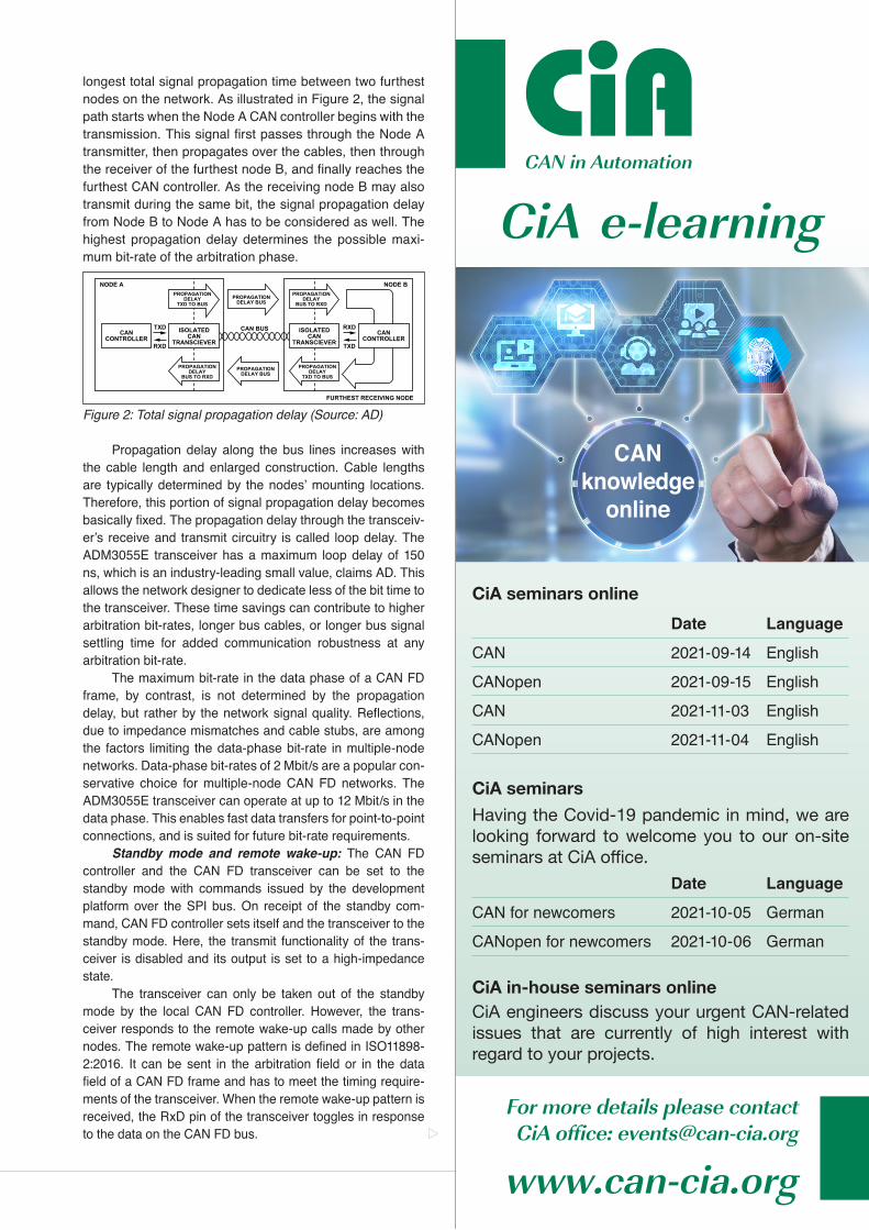
longest total signal propagation time between two furthest nodes on the network. As illustrated in Figure 2, the signal path starts when the Node A CAN controller begins with the transmission. This signal first passes through the Node A transmitter, then propagates over the cables, then through the receiver of the furthest node B, and finally reaches the furthest CAN controller. As the receiving node B may also transmit during the same bit, the signal propagation delay from Node B to Node A has to be considered as well. The highest propagation delay determines the possible maxi-mum bit-rate of the arbitration phase.
Propagation delay along the bus lines increases with the cable length and enlarged construction. Cable lengths are typically determined by the nodes’ mounting locations. Therefore, this portion of signal propagation delay becomes basically fixed. The propagation delay through the transceiv-er’s receive and transmit circuitry is called loop delay. The ADM3055E transceiver has a maximum loop delay of 150 ns, which is an industry-leading small value, claims AD. This allows the network designer to dedicate less of the bit time to the transceiver. These time savings can contribute to higher arbitration bit-rates, longer bus cables, or longer bus signal settling time for added communication robustness at any arbitration bit-rate.
The maximum bit-rate in the data phase of a CAN FD frame, by contrast, is not determined by the propagation delay, but rather by the network signal quality. Reflections, due to impedance mismatches and cable stubs, are among the factors limiting the data-phase bit-rate in multiple-node networks. Data-phase bit-rates of 2 Mbit/s are a popular con-servative choice for multiple-node CAN FD networks. The ADM3055E transceiver can operate at up to 12 Mbit/s in the data phase. This enables fast data transfers for point-to-point connections, and is suited for future bit-rate requirements.
Standby mode and remote wake-up: The CAN FD controller and the CAN FD transceiver can be set to the standby mode with commands issued by the development platform over the SPI bus. On receipt of the standby com-mand, CAN FD controller sets itself and the transceiver to the standby mode. Here, the transmit functionality of the trans-ceiver is disabled and its output is set to a high-impedance state.
The transceiver can only be taken out of the standby mode by the local CAN FD controller. However, the trans-ceiver responds to the remote wake-up calls made by other nodes. The remote wake-up pattern is defined in ISO11898-2:2016. It can be sent in the arbitration field or in the data field of a CAN FD frame and has to meet the timing require-ments of the transceiver. When the remote wake-up pattern is received, the RxD pin of the transceiver toggles in response to the data on the CAN FD bus.
NODE A NODE B
FURTHEST RECEIVING NODE
CANCONTROLLER
TXD CAN BUS
PROPAGATIONDELAY
TXD TO BUS
PROPAGATIONDELAY
BUS TO RXD
PROPAGATIONDELAY BUS
PROPAGATIONDELAY BUS
ISOLATEDCAN
TRANSCIEVERRXD
CANCONTROLLER
RXD
TXD
PROPAGATIONDELAY
BUS TO RXD
PROPAGATIONDELAY
TXD TO BUS
ISOLATEDCAN
TRANSCIEVER
Figure 2: Total signal propagation delay (Source: AD)
CiA e-learning
For more details please contact CiA office: [email protected]
www.can-cia.org
CiA seminars onlineDate Language
CAN 2021-09-14 English
CANopen 2021-09-15 English
CAN 2021-11-03 English
CANopen 2021-11-04 English
Having the Covid-19 pandemic in mind, we are looking forward to welcome you to our on-site seminars at CiA office.
CANknowledge
online
CiA seminars
Date Language
CAN for newcomers 2021-10-05 German
CANopen for newcomers 2021-10-06 German
CiA in-house seminars onlineCiA engineers discuss your urgent CAN-related issues that are currently of high interest with regard to your projects.
18 CAN Newsletter 3/2021
CAN. Implementing the switchable termination circuit with a second SSR allows for addition of a filter capacitor. The latter interacts with the split termination resistors to pro-vide a low-pass filter, reducing the common-mode noise on the bus.
Silent mode and slope control mode: The CN-0401 circuit supports bit-rate detection via a software-configu-rable trial and error function. This is possible in conjunc-tion with the silent mode of the transceiver. Silent mode disables the transceiver’s transmit channel and allows a CAN controller to produce error frames while attempting to synchronize to the bus bit-rate without to interrupt the bus traffic. The CN-0401 circuit provides access to the transceiver’s slope control mode. For low-speed signaling, slope control decreases the slew rate of the CAN-High and CAN-Low recessive-to-dominant transitions. Decreasing of the slew rate minimizes ringing and electromagnetic interference (EMI) caused by fast edges. The slope control mode should not be used for high-speed signaling.
Circuit evaluation and test
This section outlines a simple evaluation procedure for the EVAL-ADM3055E-ARDZ using the EVAL-ADICUP3029 de-velopment board. More information on the hardware and software setup is available on the company’s website.Equipment needed
PC with a USB port and operating system Windows 7 (32-bit) or higher
Serial terminal (e.g. Putty or Tera Term) Two EVAL-ADM3055E-ARDZ circuit evaluation boards Two EVAL-ADICUP3029 development boards Crosscore Embedded Studio or pre-built .hex file
Getting started1. Open the CN0401 project in Crosscore Embedded
Studio2. Check that all user-defined settings are correct, as
detailed in the EVAL-ADM3055E-ARDZ user guide3. Build the project and upload the project to the
ADICUP3029 board (alternatively, copy (drag and drop) the pre-built .hex file into the ADICUP3029 board mass storage device).
Functional test block diagram: Figure 4 shows the functional block diagram of the test setup. The PCB-teth-ered node software sets up a command line interface (CLI), which is commanded via a serial terminal running on a PC. Through the serial terminal, the user is able to command other nodes and send a remote wake-up message.
The state changes on the RxD pin are used to trigger an interrupt to the CAN FD controller. When the transceiver receives the remote wake-up pattern, it does not exit the standby mode. While development it can be determined whether to respond, or to toggle the standby pin of the transceiver to discontinue reception of the low-speed data and to return to the standby mode until the remote wake-up pattern is received again. In the standby mode, the isolated auxiliary channel of the transceiver latches in the last state. Transceiver’s integrated DC-to-DC converter continues to operate providing power to the bus side circuitry.
Isolation: Harsh environments, lengthy physical sep-aration, and different power supply sources between nodes can (and often do) have different local ground potentials. The different potentials cause currents flowing through the ground wire causing common-mode offsets and noises. Isolation of the physical bus lines breaks the ground loops and eliminates these problems. The ADM3055E trans-ceiver breaks ground loops and carries system level safety certification for the 5-kVRMS signal and power isola-tion between the CAN FD node and the CAN bus lines. For applications requiring lower isolation capabilities, the ADM3057E is available. For applications where bus-side power is available, ADM3056E is a reinforced signal iso-lated solution.
Switchable termination: For the best signal integ-rity, termination has to be implemented at both ends of a CAN network. Switchable termination allows to configure the termination location via software. This is useful for on-the-fly network reconfiguration when nodes are removed or added.
To keep the network reliability as high as possible, termination circuitry may not restrict the common-mode range. The termination circuitry may also not be affected by the common-mode range of the signal i.e. the termina-tion circuitry must remain off when set to off and remain on when set to on. To meet the required circuit character-istics, the termination circuitry on the EVAL-ADM3055E-ARDZ evaluation board floats with the transmitting node using very compact optically-isolated SPST (single pole single throw) solid state relays (SSR).
Controlling the relays from the auxiliary isolated chan-nel of the transceiver means that the relays do not bridge the isolation gap. Thus, the relays are not required to pro-
vide a safety isolation function and can have the smallest possible package to save the printed circuit board (PCB) area.
The 120-Ohm termi- nation resistance (Fig-ure 3) can be accom-plished with a single resistor. However, split-ting the resistor into two 60-Ohm resistors offers an inexpensive measure of electrostatic discharge (ESD) protection to both relay pins exposed to the
R2160.4Ω
K1AQY221RV
AUXOUT
CANL
CANH
K2AQY221RV
R203.48kΩ
R2260.4Ω
C94700pF
Figure 3: Switchable 120-Ohm termination resistance using Photomos relays controlled via an auxiliary channel (Source: AD) COMMAND-LINE INTERFACE
CAN BUS NODE CAN BUS NODE
EVAL-ADM3055E-ARDZ
EVAL-ADICUP3029 EVAL-ADICUP3029
P1ORP4
CANH
CANLEVAL-ADM3055E-ARDZ
USB CABLE
P1ORP4
Figure 4: EVAL-ADM3055E-ARDZ functional test block diagram (Source: AD)
Engi
neer
ing
19CAN Newsletter 3/2021
Test setup: A CAN node is set up by mounting the EVAL-ADM3055E-ARDZ atop the EVAL-ADICUP3029 using the Arduino-compatible headers, as shown in Figure 5.
Communication and remote wake-up test: With the sample software built and loaded on two different CAN nodes, the two boards (when connected) communicate with each other through a CAN FD connection. Figure 6 shows a two-node CAN connection.
Default arbitration and data bit-rates are 500 kbit/s and 2 Mbit/s, respectively. The boards are connected to the PC via a USB cable. Each node has its own CLI running on a serial terminal. This configuration sets up a two-way CAN FD communication between the devices acting as two indepen-dent CAN nodes.
At first, the nodes are in sleep mode. Via the CLI a node can be commanded to wake up and to send an Ascii mes-sage via CAN. The message transmission has a timeout of 5 s and is cyclically sent until it is acknowledged by the other node. The message, particularly the slower arbitration phase, wakes up the other node. The latter acknowledges the mes-sage and displays it on the serial terminal connected to its node. Then, both nodes reenter the sleep mode.
Figure 5: CAN node setup using EVAL-ADM3055E-ARDZ and EVAL-ADICUP3029 (Source: AD)
Figure 6: Two-node CAN connection test setup (Source: AD)
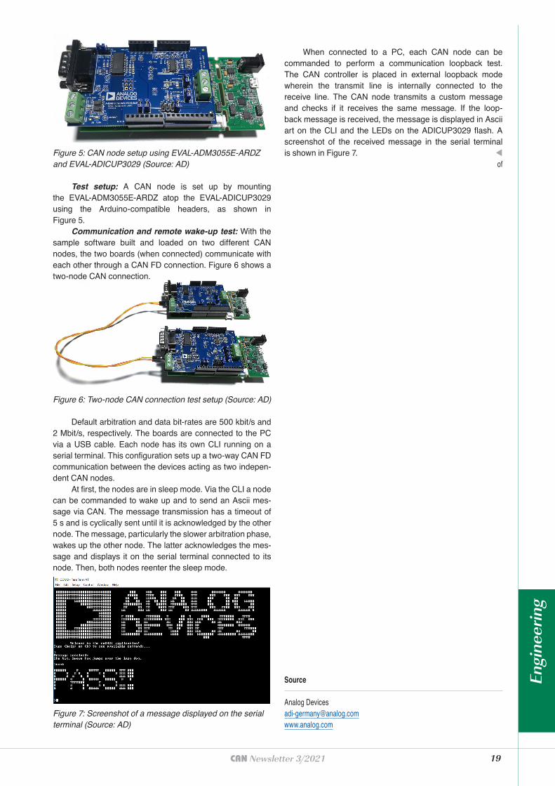
When connected to a PC, each CAN node can be commanded to perform a communication loopback test. The CAN controller is placed in external loopback mode wherein the transmit line is internally connected to the receive line. The CAN node transmits a custom message and checks if it receives the same message. If the loop-back message is received, the message is displayed in Ascii art on the CLI and the LEDs on the ADICUP3029 flash. A screenshot of the received message in the serial terminal is shown in Figure 7. t
of
Figure 7: Screenshot of a message displayed on the serial terminal (Source: AD)
AuthorAnalog Devicesadi-ger-
www.analog.com
Source
Analog [email protected]
Engi
neer
ing