
Burst Mode Q:switched Laser Pulses for Plasma Excitation in LIBS

General DescriptionThe DS1863 controls and monitors all the burst-modetransmitter and video receiver biasing functions for apassive optical network (PON) transceiver. It has anAPC loop with tracking-error compensation that pro-vides the reference for the laser driver’s bias currentand a temperature-indexed lookup table (LUT) thatcontrols the modulation current. It continually monitorsfor high output current, high bias current, and low andhigh transmit power with its internal fast comparators toensure that laser shutdown for eye safety requirementsare met without adding external components. Five ADCchannels monitor VCC, internal temperature, and threeexternal monitor inputs (MON1, MON2, MON3) that canbe used to meet transmitter and receive monitoringrequirements.
ApplicationsBPON, GPON, and GEPON Burst-Mode Transmitters
Laser Control and Monitoring
Broadband Local Access
Features♦ Meets BPON, GPON, and GEPON Timing
Requirements for Burst-Mode Transceivers
♦ Bias Current Control Provided by APC Loop withTracking Error Compensation
♦ Modulation Current Is Controlled by aTemperature-Indexed Lookup Table
♦ Supports 0dB, -3dB, -6dB Power LevelingSettings with No Additional Calibration
♦ Internal Direct-to-Digital Temperature Sensor
♦ Five Analog Monitor Channels: Temperature, VCC,MON1, MON2, and MON3
♦ Comprehensive Fault Management System withMaskable Laser Shutdown Capability
♦ Two-Level Password Access to ProtectCalibration Data
♦ 120 Bytes of Password 1 (PW1) Protected Nonvolatile Memory
♦ 128 Bytes of Password 2 (PW2) Protected Nonvolatile Memory
♦ I2C-Compatible Interface for Calibration andMonitoring
♦ Operating Voltage: 2.85V to 3.9V
♦ Operating Temperature: -40°C to +95°C
♦ 16-Pin, Lead-Free TSSOP Package
DS
18
63
Burst-Mode PON ControllerWith Integrated Monitoring
______________________________________________ Maxim Integrated Products 1
19-4883; Rev 2; 8/09
For pricing, delivery, and ordering information, please contact Maxim Direct at 1-888-629-4642,or visit Maxim’s website at www.maxim-ic.com.
+Denotes a lead(Pb)-free/RoHS-compliant package.T&R = Tape and reel.
Ordering Information
PART TEMP RANGE PIN-PACKAGE
DS1863E+ -40°C to +95°C 16 TSSOP
DS1863E+T&R -40°C to +95°C 16 TSSOP16
15
14
13
12
11
10
1
2
3
4
5
6
7
VCC
BMD
MOD
BIASTX-F
N.C.
TX-D
BEN
TOP VIEW
GND
MON3
MON2SCL
SDA
98 MON1GND
FETG
TSSOP(173 mils)
DS1863
+
Pin Configuration

DS
18
63
Burst-Mode PON ControllerWith Integrated Monitoring
2 _____________________________________________________________________
ABSOLUTE MAXIMUM RATINGS
RECOMMENDED OPERATING CONDITIONS(TA = -40°C to +95°C, unless otherwise noted.)
Stresses beyond those listed under “Absolute Maximum Ratings” may cause permanent damage to the device. These are stress ratings only, and functionaloperation of the device at these or any other conditions beyond those indicated in the operational sections of the specifications is not implied. Exposure toabsolute maximum rating conditions for extended periods may affect device reliability.
Voltage on VCC, SDA and SCL Pin Relative to Ground....................................................................-0.5V to 6VVoltage on BEN, TX-D, TX-F, MON1–MON3,BMD Relative to Ground...............................-0.5V to VCC + 0.5V
(subject to not exceeding +6V)
Operating Temperature Range ...........................-40°C to +95°CProgramming Temperature Range .........................0°C to +70°CStorage Temperature Range .............................-55°C to +125°CSoldering Temperature ...................See J-STD-020 specification
PARAMETER SYMBOL CONDITIONS MIN TYP MAX UNITS
Supply Voltage VCC (Note 1) +2.85 3.9 V
H i gh- Level Inp ut V ol tage ( SD A, S C L, BE N) VIH:1 0.7 x VCC VCC + 0.3 V
Low- Level Inp ut V oltag e ( S DA, SC L, BE N ) VIL:1 -0.3 0.3 x VCC V
High-Level Input Voltage (TX-D) VIH:2 2.0 VCC + 0.3 V
Low-Level Input Voltage (TX-D) VIL:2 -0.3 0.8 V
ELECTRICAL CHARACTERISTICS(VCC= +2.85V to +3.9V, TA = -40°C to +95°C, unless otherwise noted.)
PARAMETER SYMBOL CONDITIONS MIN TYP MAX UNITS
Supply Current ICC (Notes 1, 2) 5 7 mA
Output Leakage (SDA, TX-F) ILO 1 µA
IOL = 4mA 0.4Low-Level Output Voltage(SDA, TX-F, FETG)
VOLIOL = 6mA 0.6
V
High-Level Output Voltage (FETG) VOH IOH = 4mA (Note 2) VCC – 0.4 V
FETG Before Recall (Note 3) 10 100 nA
Inp ut Leakag e C ur r ent ( S C L, BE N , TX - D ) ILI:1 1 µA
Digital Power-On Reset POD 1.0 2.2 V
Analog Power-On Reset POA 2.1 2.75 V
ANALOG INPUT CHARACTERISTICS (BMD)(VCC = +2.85V to +3.9V, TA = -40°C to +95°C, unless otherwise noted.)
PARAMETER SYMBOL CONDITIONS MIN TYP MAX UNITS
BMD Full-Scale Voltage Range VAPC (Note 4) 2.5 V
Resolution (Note 4) 8 bits
VAPC Error TA = +25°C (Note 5) -1.75 +1.75 %FS
VAPC Integral Nonlinearity -1 +1 LSB
VAPC Differential Nonlinearity -1 +1 LSB
VAPC Temp Drift -2.5 +2.5 %FS
Input Resistance 35 50.0 65 kΩ

DS
18
63
Burst-Mode PON ControllerWith Integrated Monitoring
_____________________________________________________________________ 3
ANALOG OUTPUT CHARACTERISTICS(VCC= +2.85V to +3.9V, TA = -40°C to +95°C, unless otherwise noted.)
PARAMETER SYMBOL CONDITIONS MIN TYP MAX UNITS
BIAS Current IBIAS (Note 1) 1.2 mA
IBIAS Shutdown Current IB IA S : OF F 10 100 nA
Voltage at IBIAS 0.7 1.2 1.4 V
MOD Full-Scale Voltage VMOD (Note 6) 1.25 V
MOD Output Impedance (Note 7) 3.14 kΩVMOD Error TA = +25°C (Note 8) -1.25 +1.25 %FS
VMOD Integral Nonlinearity -1 +1 LSB
VMOD Differential Nonlinearity -1 +1 LSB
VMOD Temperature Drift -2 +2 %FS
CONTROL LOOP AND QUICK-TRIP TIMING CHARACTERISTICS(VCC= +2.85V to +3.9V, TA = -40°C to +95°C, unless otherwise noted.)
PARAMETER SYMBOL CONDITIONS MIN TYP MAX UNITS
First BMD Sample Following BEN tFIRST (Note 9)
Remaining Updates During BEN tREP (Note 9)
BEN High Time tBEN:HIGH 420 ns
BEN Low Time tBEN:LOW 96 ns
BIAS and MOD Turn-Off Delay tOFF 5 µs
BIAS and MOD Turn-On Delay tON 5 µs
FETG Turn-On Delay tFETG:ON 5 µs
FETG Turn-Off Delay tFETG:OFF 5 µs
Binary Search Time tSEARCH (Note 10) 5 13BIAS
Samples
ADC Round-Robin Time tRR 65 ms
ANALOG VOLTAGE MONITORING(VCC = +2.85V to +3.9V, TA = -40°C to +95°C, unless otherwise noted.)
PARAMETER SYMBOL CONDITIONS MIN TYP MAX UNITS
ADC Resolution 13 Bits
Input/Supply Accuracy (MON1, MON2, MON3, VCC)
ACC At factory setting 0.25 0.5 %FS
Update Rate for Temperature, MON1, MON2, MON3, VCC
tFRAME:1 52 70 ms
Input/Supply Offset (MON1, MON2, MON3, VCC)
VOS (Note 11) 0 5 LSB
MON1, MON2, MON3 2.5 Factory Setting VCC Full scales are user programmable 6.5536
V

DS
18
63
Burst-Mode PON ControllerWith Integrated Monitoring
4 _____________________________________________________________________
NONVOLATILE MEMORY CHARACTERISTICS(VCC = +2.85V to +3.9V, unless otherwise noted.)
PARAMETER SYMBOL CONDITIONS MIN TYP MAX UNITS
EEPROM Write Cycles +70°C 50,000
I2C AC ELECTRICAL CHARACTERISTICS(VCC = +2.85V to +3.9V, TA = -40°C to +95°C, unless otherwise noted, see Figure 9.)
PARAMETER SYMBOL CONDITIONS MIN TYP MAX UNITS
SCL Clock Frequency fSCL (Note 12) 0 400 kHz
Clock Pulse-Width Low tLOW 1.3 µs
Clock Pulse-Width High tHIGH 0.6 µs
Bus Free Time Between STOP andSTART Condition
tBUF 1.3 µs
START Hold Time tHD:STA 0.6 µs
START Setup Time tSU:STA 0.6 µs
Data-In Hold Time tHD:DAT 0 0.9 µs
Data-In Setup Time tSU:DAT 100 ns
Rise Time of Both SDA andSCL Signals
tR (Note 13) 20 + 0.1CB 300 ns
Fall Time of Both SDA andSCL Signals
tF (Note 13) 20 + 0.1CB 300 ns
STOP Setup Time tSU:STO 0.6 µs
Capacitive Load for Each Bus Line CB (Note 13) 400 pF
EEPROM Write Time tW (Note 14) 20 ms
Note 1: All voltages are referenced to ground. Currents into the IC are positive and out of the IC are negative.Note 2: Digital Inputs are at rail. FETG is disconnected SDA = SCL = 1.Note 3: See the Safety Shutdown (FETG) Output section for details.Note 4: Eight ranges allow the full-scale range to change from 625mV to 2.5V.Note 5: This specification applies to the expected full-scale value for the selected range. See the Comp Ranging byte for available
full-scale ranges.Note 6: Eight ranges allow the full-scale range to change from 312.5mV to 1.25V.Note 7: The output impedance of the DS1863 is proportional to its scale setting. For instance, if using the 1/2 scale, the output
impedance would be 1.5kΩ.Note 8: This specification applies to the expected full-scale value for the selected range. See the Mod Ranging byte for available
full-scale ranges.Note 9: See the APC/Quick-Trip Sample Timing section for details.Note 10: Assuming an appropriate initial step is programmed that would cause the power to exceed the APC set point within 4
steps, the bias current will be within 1% within the time specified by the binary search time.Note 11: Guaranteed by design.Note 12: I2C interface timing shown is for fast-mode (400kHz) operation. This device is also backward-compatible with I2C stan-
dard-mode timing.Note 13: CB—total capacitance of one bus line in picofarads.Note 14: EEPROM write begins after a STOP condition occurs.

DS
18
63
Burst-Mode PON ControllerWith Integrated Monitoring
Typical Operating Characteristics(VCC = 3.3V, TA = +25°C, unless otherwise noted.)
2.50
2.95
2.80
2.65
3.10
3.25
3.40
3.55
3.70
3.85
4.00
2.85 3.853.35 4.35 4.85 5.35
SUPPLY CURRENT vs. SUPPLY VOLTAGE
DS18
63 to
c01
VCC (V)
SUPP
LY C
URRE
NT (m
A)
SDA = SCL = VCC
+95°C
-40°C+25°C
3.00
3.15
3.10
3.05
3.25
3.20
3.45
3.40
3.35
3.30
3.50
-40 -20 0 20 40 60 80 100
SUPPLY CURRENT vs. TEMPERATURE
DS18
63 to
c02
TEMPERATURE (°C)
SUPP
LY C
URRE
NT (m
A)
VCC = 2.85V
VCC = 3.9V
SDA = SCL = VCC
-1.0
-0.4
-0.6
-0.8
-0.2
0
0.2
0.4
0.6
0.8
1.0
0 10050 150 200 250
MOD DNL
DS18
63 to
c03
MOD INPUT CODE (DEC)
MOD
DNL
(LSB
)
-1.0
-0.4
-0.6
-0.8
-0.2
0
0.2
0.4
0.6
0.8
1.0
0 10050 150 200 250
MOD INL
DS18
63 to
c04
MOD INPUT CODE (DEC)
MOD
INL
(LSB
)
0
20
10
40
30
60
50
70
90
80
100
001 010000 011 100 101 110 111
CALCULATED AND DESIRED % CHANGEIN VMOD vs. MOD RANGING
DS18
63 to
c05
MOD RANGING VALUE (DEC)
CHAN
GE IN
VM
OD (%
)
DESIRED VALUE
CALCULATED VALUE
0
20
10
40
30
60
50
70
90
80
100
DESIRED AND CALCULATED CHANGEIN VBMD vs. COMP RANGING
DS18
63 to
c06
COMP RANGING (DEC)
CHAN
GE IN
VBM
D (%
)
001 010000 011 100 101 110 111
DESIRED VALUE
CALCULATED VALUE
-1.0
-0.4
-0.6
-0.8
-0.2
0
0.2
0.4
0.6
0.8
1.0
0 1.00.5 1.5 2.0 2.5
MON1–3 DNL
DS18
63 to
c07
MON1–3 INPUT VOLTAGE (V)
MON
1–3
DNL
(LSB
)
USING FACTORY-PROGRAMMEDFULL-SCALE VALUE OF 2.5V
-1.0
-0.4
-0.6
-0.8
-0.2
0
0.2
0.4
0.6
0.8
1.0
0 1.00.5 1.5 2.0 2.5
MON1–3 INL
DS18
63 to
c08
MON1–3 INPUT VOLTAGE (V)
MON
1–3
INL
(LSB
)
USING FACTORY-PROGRAMMEDFULL-SCALE VALUE OF 2.5V
-1.0
-0.4
-0.6
-0.8
-0.2
0
0.2
0.4
0.6
0.8
1.0
0 10050 150 200 250
VBMD INL vs. APC INDEXDS
1863
toc0
9
APC INDEX (DEC)
V BM
D IN
L (L
SB)
_____________________________________________________________________ 5

DS
18
63
Burst-Mode PON ControllerWith Integrated Monitoring
6 _____________________________________________________________________
Pin Description
PIN NAME DESCRIPTION
1 BEN Burst Enable Input. Triggers the sampling of the APC and Quick-trip monitors.
2 TX-D Transmit Disable Input. Disables BIAS and MOD outputs.
3 N.C. No Connection
4 TX-F Transmit Fault Output. Open-drain.
5 FETG Output to FET Gate. Signals an external N or P Channel MOSFET to enable/disable the laser’s current.
6 SDA I2C Serial Data I/O
7 SCL I2C Serial Clock Input
8 GND Ground
9 MON1
10 MON2
11 MON3
External Analog Inputs. The voltage at these pins is digitized by the internal analog-to-digital converterand can be read through the I2C interface. Alarm and warning values can be assigned to interrupt theprocessor based on the ADC result.
12 GND Ground
13 BIAS Bias Current Output. This current DAC generates the bias current reference for the MAX3643.
14 MODModulation Output Voltage. This 8-bit voltage output has 8 full-scale ranges from 1.25V to 0.3125V.This pin is connected to the MAX3643’s VMSET input to control the modulation current.
15 BMD Monitor Diode Input (Feedback Voltage, Transmit Power Monitor)
16 VCC Power Supply Input

DS
18
63
Burst-Mode PON ControllerWith Integrated Monitoring
_____________________________________________________________________ 7
BMD
BEN
MON2
MON1
MON3
SCL
SDA
GND
VCC
TX-D
BIAS
MOD
FETG
TX-F
HBIAS QUICKTRIP LIMIT
HTXP QUICKTRIP LIMIT
LTXP QUICKTRIP LIMIT
APC SETPOINT FROMTRACKING ERROR TABLE
LATCHENABLE
VCC
TEMPSENSOR
I2CINTERFACE
SAMPLECONTROL
8-BIT DACW/SCALING DIGITAL APC
INTEGRATOR13-BITDAC
ANAL
OG M
UX
MODULATION LOOKUPTABLE (TABLE 04h)
8-BIT DACW/SCALING
MAX BIASQUICKTRIP
INTERRUPTMASK
INTERRUPTLATCH
INTERRUPTMASK
INTERRUPTLATCH
POWER ON ANALOGVCC > VPOA
NONMASKABLEINTERRUPT
13-BITADC
DS1863 MEMORY ORGANIZATION
SRAM RESET
RIGHTSHIFT
TABLE 01hEEPROM
PW1USER MEMORY
AND ALARMTRAPS
TABLE 02hEEPROM
CONFIGURATIONAND
CALIBRATION
TABLE 03hEEPROM
PW2USER MEMORY
LOWER MEMORYEEPROM/SRAM
ADC CONFIG/RESULTSSYSTEM STATUS BITS
ALARM/WARNING COMPARISON RESULTS/THRESHOLDS
TABLE 04hEEPROM
MODULATIONLUT
TABLE 05hEEPROM
TRACKINGERROR LUT
DIGITAL LIMITCOMPARATOR FOR
ADC RESULTS
DS1863
MUX
MUX
MUX
Block Diagram

DS
18
63
Burst-Mode PON ControllerWith Integrated Monitoring
8 _____________________________________________________________________
Detailed DescriptionThe DS1863 integrates the control and monitoring func-tionality required to implement a PON system usingMaxim’s MAX3643 compact burst mode laser driver.The compact laser driver solution offers a considerablecost benefit by integrating control and monitoring fea-tures in low power CMOS process, while leaving onlythe high speed portions to the laser driver IC.
APC ControlBIAS current is controlled by an Average Power Control(APC) loop. The APC loop uses digital techniques toovercome the difficulties associated with controllingburst mode systems.
The APC loop’s feedback is the monitor diode (BMD)current, which is converted to a voltage using an exter-nal resistor. The feedback voltage is compared to an 8-bit scaleable voltage reference, which determines theAPC set point of the system. Scaling of the referencevoltage along with the modulation output can be uti-lized to implement GPON power leveling.
The DS1863 has a Lookup Table to allow the APC setpoint to change as a function of temperature to com-pensate for Tracking Error (TE). The TE LUT (Table05h), has 36 entries that determine the APC setting in4°C windows between -40°C to +100°C.
Ranging of the APC DAC is possible by programming asingle byte in Table 02h.
Typical Operating Circuit
BEN+
BEN-
DISMAX3643
IN-
IN+
OUT-
BIAS-
BIAS+
MDINCOMPACT BURST MODE
LASER DRIVER
DS1863BURST MODE
MONITOR/CONTROL CIRCUIT
MDOUT
OUT+
VCC
TX-F
TX-D
SCL
SDA
MON2
MON3
FETG
MON1
BMD
3.3V
VMSE
T
MOD
SET
VREF
IMAX
GND
BIAS
SET
BENO
UT
MOD BIAS BEN
BIAS
MON
VBES
T
TRANSMIT POWER
RECEIVE POWER
I2C COMMUNICATION
FAULT OUTPUT
DISABLE INPUT

DS
18
63
Burst-Mode PON ControllerWith Integrated Monitoring
_____________________________________________________________________ 9
Modulation ControlThe MOD voltage is controlled using an internal tem-perature indexed Lookup Table.
The MOD output is an 8-bit scaleable voltage output thatinterfaces with the MAX3643’s VMSET input. An externalresistor to ground from the MAX3643’s MODSET pin setsthe maximum current the voltage at VMSET input canproduce for a given output range. This resistor valueshould be chosen to produce the maximum modulationcurrent the laser type requires over temperature. Themodulation LUT can be programmed in 2°C incrementsover the -40°C to +102°C range to provide temperaturecompensation for the laser’s modulation. The modulationDAC’s scaling can be used (with APC scaling) to imple-ment GPON power leveling with a single LUT that worksfor all three power levels.
Ranging of the MOD DAC is possible by programminga single byte in Table 02h.
BIAS and MOD Output During Initial Power-Up
On power-up the modulation and bias outputs willremain off until VCC is above VPOA, a temperature con-version has been completed, and if the VCC LO ADCalarm is enabled, then a VCC conversion above thecustomer defined VCC low alarm level has cleared theVCC low alarm. Once all of these conditions are satis-
fied, the MOD output will be enabled with the valuedetermined by the temperature conversion and themodulation LUT.
When the MOD output is enabled and BEN is high, theIBIAS DAC output will be turned on to a value equal toISTEP (see above). The start-up algorithm checks if thisbias current causes a feedback voltage above the APCset-point, and if it does not it continues increasing theIBIAS by ISTEP until the APC set-point is exceeded.When the APC set point is exceeded, the device willbegin a binary search to quickly reach the bias currentcorresponding to the proper power level. After the bina-ry search is completed the APC integrator is enabled,and single LSB steps are taken to tightly control theaverage power.
All quick-trip and ADC alarm flags are masked until thebinary search is completed. However, the BIAS MAXalarm is monitored during this time to prevent the biasoutput from exceeding MAX IBIAS. During the bias cur-rent initialization, the bias current is not allowed toexceed MAX IBIAS. If this occurs during the ISTEPsequence then the binary search routine is enabled. IfMAX IBIAS is exceeded during the binary search, thenthe next smaller step is activated. ISTEP or binary incre-ments that would cause IBIAS to exceed MAX IBIAS arenot taken. Many of the alarm sources are likely to trip
1 2 3 4 5 6 7 8 9 10 11 12 13
tON
VPOA
BINARY SEARCHAPC
INTEGRATOR ON
tSEARCH
POWER-UP TIMING
MODVOLTAGE
BIASCURRENT
VCC
BIASSAMPLE
ISTEP
4x ISTEP
3x ISTEP
2x ISTEP
Figure 1. DS1863 Power-Up.

DS
18
63
Burst-Mode PON ControllerWith Integrated Monitoring
10 ____________________________________________________________________
during start-up. Masking the alarms until the completionof the binary search prevents false alarms.
ISTEP is programmed by the customer using the Start-up Step register. This value should be programmed tothe maximum safe current increase that is allowableduring start-up. If this value is programmed too low, theDS1863 will still operate, but it could take significantlylonger for the algorithm to converge and hence to con-trol the average power.
If a fault is detected, and TX-D is toggled to re-enable theoutputs, the DS1863 will power up following a similarsequence to an initial power up. The only difference isthat the DS1863 already has determined the present tem-perature, so the tINIT time is not required for the DS1863to recall the APC and MOD set points from EEPROM.
BIAS and MOD Output as a Functionof Transmit Disable (TX-D)
If TX-D is asserted (logic 1) during operation, the out-puts will immediately turn off (tOFF). When TX-D isdeasserted (logic 0), the DS1863 will turn on the MODoutput with the value associated with the present tem-perature, and initialize the IBIAS using the same searchalgorithm as done at start-up. Soft TX-D (LowerMemory, Register 6Eh) when asserted would allow asoftware control identical to the TX-D pin.
APC/Quick-Trip Shared Comparator TimingThe DS1863’s input comparator is shared between theAPC control loop and the three quick-trip alarms(HTXP, LTXP and HBIAS). The comparator polls thealarms in a round-robin multiplexed sequence. Six ofevery eight of the comparator readings will be used forAPC Loop bias current control. The other two updateswill be used to check the HTXP/LTXP (Monitor Diodevoltage) and the HBIAS (MON1) signals against the
internal APC and BIAS reference. The HTXP/LTXP com-parison will check HTXP if the last bias-update compar-ison was above the APC set-point, and LTXP if the lastbias update comparison was below the APC set-point.
The DS1863 has a programmable comparator sampletime based on an internally generated clock to facilitate awide variety of external filtering options suitable for burstmode transmitter data rates between 155Mbits/s and1250Mbits/s. The rising edge of burst enable (BEN) trig-gers the sample to occur, and the Sample Rate registerdetermines the delay. The internal clock is asynchronousto BEN, causing a 100ns uncertainty as to when the firstsample will occur following BEN. After the first sampleoccurs, subsequent samples will occur on a regularinterval. The following sample rate options are available.
Comparisons of the HTXP, LTXP, and HBIAS quick-tripalarms will not occur during the burst enable low time.Any quick-trip alarm that is detected will by defaultremain active until a subsequent comparator sampleshows the condition no longer exists.
A second bias current monitor compares the DS1863’sbias current DAC’s code to a digital value stored in theMAX IBIAS register. This comparison is made everybias current update to ensure that a high bias currentwill be quickly detected.
TX-D TIMING (NORMAL OPERATION)
TX-D
IBIAS
IMOD tOFF tON
tONtOFF
Figure 2. TX-D Timing (Output Disabled During Normal OperatingConditions).
SR3–SR0
MINIMUM TIMEFROM BEN TO FIRST
SAMPLE (tFIRST)±50ns
REPEATED SAMPLEPERIOD FOLLOWINGFIRST SAMPLE (tREP)
0000b 350ns 800ns
0001b 550ns 1200ns
0010b 750ns 1600ns
0011b 950ns 2000ns
0100b 1350ns 2800ns
0101b 1550ns 3200ns
0110b 1750ns 3600ns
0111b 2150ns 4400ns
1000b 2950ns 6000ns
1001b* 3150ns 6400ns
*All codes greater than 1001b (1010b–111b) use the maximumsample time of code 1001b.

DS
18
63
Burst-Mode PON ControllerWith Integrated Monitoring
____________________________________________________________________ 11
Monitors And Fault DetectionMonitors
Monitoring functions on the DS1863 include four quick-trip comparators and five ADC channels
This monitoring combined with the interrupt masksdetermines when/if the DS1863 shuts down its outputsand triggers the TX-F and FETG outputs. All of the mon-itoring levels and interrupt masks are user programma-ble with the exception of POA, which trips at a fixedrange and is non-maskable for safety reasons.
Four Quick-Trip Monitors And AlarmsFour quick-trip monitors are provided to detect potentiallaser safety issues. These monitor
1) High Bias Current (HBIAS)
2) Low Transmit Power (LTXP)
3) High Transmit Power (HTXP)
4) Max Output Current (MAX IBIAS)
The high and low transmit power quick-trip registers(HTXP and LTXP) set the thresholds used to compareagainst the BMD voltage to determine if the transmitpower is within specification. The HBIAS quick-tripcompares the MON1 input (generally from theMAX3643 bias monitor output) against its threshold set-ting to determine if the present bias current is abovespecification. The Max Bias quick-trip is a digital com-parison that determines if the Bias Output code indi-cates the bias current is above specification. The biascurrent will not be allowed to exceed the value set inthis register. When the DS1863 detects the bias is atthe limit it will set the BIAS MAX status bit and hold thebias current at the MAX IBIAS level. The quick-trips arerouted to the TX-F and FETG outputs via interruptmasks to allow combinations of these alarms to beused to trigger these outputs. Any time FETG is trig-gered the DS1863 will also disable its outputs. All the
quick-trip alarm levels and masks are programmablethrough the I2C interface.
Five ADC Monitors And AlarmsThe ADC monitors five channels that measure tempera-ture (internal temp sensor), VCC, MON1, MON2, andMON3 using an analog multiplexer to measure themround robin with a single ADC. Each channel has acustomer programmable full scale range and offsetvalue that will be factory programmed to default value(see below). Additionally, MON1, MON2, and MON3have the ability to right shift results by up to 7 bitsbefore the results are compared to alarm thresholds orread over the I2C bus. This allows customers with spec-ified ADC ranges to calibrate the ADC full scale to afactor of 1/2n of their specified range to measure smallsignals. The DS1863 can then right shift the results by nbits to maintain the bit weight of their specification.
The ADC results (after right shifting, if used) are com-pared to high alarm thresholds (to check if the resultsexceeded this threshold), the low alarm thresholds (tocheck if the ADC results are below this threshold) andthe warning threshold after each conversion (20 com-parisons total), and the corresponding alarms are setwhich can be used to trigger the TX-F or FETG outputs.These ADC thresholds are user programmable via theI2C interface, as are the masking registers that can be
APC LOOP/QUICK TRIP SAMPLE TIMING
LAST BURST'SBIAS SAMPLE
BEN
BIAS DAC
CODE
QUICK-TRIPSAMPLE TIMES
HBIASSAMPLE
tFIRST
tREPH/LTXP
SAMPLE
BIASSAMPLE
BIASSAMPLE
BIASSAMPLE
BIASSAMPLE
BIASSAMPLE
BIASSAMPLE
BIASSAMPLE
Figure 3. APC/Quick-Trip Alarm Sample Timing.
ADC Default Monitor Full Scale Ranges
SIGNAL (UNITS)+ FS
SIGNAL+ FSHEX
- FSSIGNAL
- FSHEX
Temperature (oC) 127.996 7FFF -128 8000
VCC (V) 6.5528 FFF8 0V 0000
MON1, MON2,MON3 (V)
2.4997 FFF8 0V 0000

DS
18
63
Burst-Mode PON ControllerWith Integrated Monitoring
12 ____________________________________________________________________
used to prevent the alarms from triggering the TX-F andFETG outputs. See below for more detail on the TX-Fand FETG outputs.
ADC TimingThere are five analog channels that are digitized in around robin fashion in the order shown in Figure 4. Thetotal time required to convert all five channels is tRR(see electrical specifications for details).
Right Shifting A/D Conversion ResultIf the weighting of the ADC digital reading must con-form to a Predetermined Full-Scale (PFS) value definedby a specification, then right shifting can be used toadjust the PFS analog measurement range while main-taining the weighting of the ADC results. The DS1863’srange is wide enough to cover all requirements; whenmaximum input value is far short of the FS value, rightshifting can be used to obtain greater accuracy. Forinstance, the maximum voltage might be 1/8 of thespecified PFS value, so only 1/8 of the converter’srange is effective over this range. An alternative is tocalibrate the ADC’s full scale range to 1/8 the readablePFS value and use a right-shift value of 3. With thisimplementation, the resolution of the measurement hasincreased by a factor of 8, and because the result isdigitally divided by 8 by right shifting, the bit weight ofthe measurement still meets the standard.
The right shift operation on the A/D converter results iscarried out based on the contents of Right Shift ControlRegisters (Table 02h Registers 8Eh to 8Fh) in EEPROM.Three analog channels: MON1 to MON3 each have 3bits allocated to set the number of right shifts. Up to 7right shift operations are allowed and will be executedas a part of every conversion before the results arecompared to the high and low alarm levels, or loadedinto their corresponding measurement registers 62h to
69h. This is true during the setup of internal calibrationas well as during subsequent data conversions.
Transmit Fault (TX-F) OutputThe TX-F output has masking registers for the five ADCalarms and the four QT alarms to select which compar-isons cause it to assert. In addition, the FETG alarm isselectable via the TX-F mask to cause TX-F to assert.All alarms, with the exception of FETG, will only causeTX-F to remain active while the alarm condition persists.However, the TX-F latch bit can enable the TX-F outputto remain active until it is cleared by the TX-F reset bit,TX-D, soft TX-D, or by power cycling the part. If theFETG output is configured to trigger TX-F, then it is indi-cating that the DS1863 is in shutdown, and will requireTX-D, soft TX-D, or cycling power to reset. The ADCand Quick-trip alarms (with the exception of BIAS MAX)are ignored for the first 8-10 bias current updates dur-ing power up. Only enabled alarms will activate TX-F.
The following table shows TX-F as a function of TX-Dand the alarm sources.
Safety Shutdown (FETG) OutputThe FETG output has masking registers (separate fromTX-F) for the five ADC alarms and the four QT alarms toselect which comparisons cause it to assert. Unlike TX-F,
NORMAL ADC SAMPLE TIMING
TEMP VCC MON1 MON2 MON3 TEMP VCC
ONE ROUND-ROBIN ADC CYCLE
MON3
tRR
Figure 4. ADC Round-Robin Timing.
If VCC low alarm is set for either the TX-F or FETG output, the Round Robin timing will cycle between only TEMP and VCC.
TX-F as a Function of TX-D and AlarmSources
VCC > VPOA TX-DNON-MASKEDTX-F ALARM
TX-F
No X X 1
Yes 0 0 0
Yes 0 1 1
Yes 1 X 0

DS
18
63
Burst-Mode PON ControllerWith Integrated Monitoring
____________________________________________________________________ 13
FETG output is always latched in case it is triggered byan unmasked alarm condition. Its output polarity is pro-grammable to allow an external N or P MOSFET to openduring alarms to shut off the laser diode current. If theFETG output triggers indicating the DS1863 is in shut-down, then it requires TX-D, soft TX-D, or cycling powerto be reset. Under all conditions when the analog outputsare re-initialized after being disabled, all the alarms withthe exception of the VCC low ADC alarm will be cleared.The VCC low alarm must remain active to prevent the out-put from attempting to operate when inadequate VCCexists to operate the laser driver. Once adequate VCC ispresent to clear the VCC low alarm, the outputs will beenabled following the same sequence as power up.
As mentioned before the FETG is an output used to dis-able the laser current via a series N or P MOSFET. Thisrequires that the FETG output is capable of sinking orsourcing current. Because the DS1863 will not know if itshould sink or source current before VCC exceedsVPOA, which triggers the EE recall, this output will behigh impedance when VCC is below VPOA. (see “LowVoltage Operation” section for details and diagram).The application circuit must use a pull-up or pull-downresistor on this pin that pulls FETG to the alarm/shut-down state (high for a PMOS, low for a NMOS). OnceVCC is above VPOA, the DS1863 will pull the FETG out-put to the state determined by the FETG DIR bit (Table02h, Register 89h). FETG DIR will be 0 if an NMOS isused and 1 if a PMOS is used.
Determining Alarm Causes Using The I2C Interface
To determine the cause of the TX-F or FETG alarm, thesystem processor can read the DS1863’s Alarm TrapBytes (ATB) through the I2C interface (in Table 01h). TheATB have a bit for each alarm. Any time an alarm occurs,regardless of the mask bit’s state, the DS1863 sets thecorresponding bit in the ATB. Active ATB bits will remainset until written to zeros via the I2C interface. On powerup the ATB will be zeros until alarms dictate otherwise.
Die IdentificationDS1863 will have an ID hard coded to its die. Two reg-isters (Table 02h bytes 86h–87h) are assigned for thisfeature. Byte 86h will read 63h to identify the part as theDS1863, byte 87h will read to A1h (for A1 die revision).
Low-Voltage OperationThe DS1863 contains two Power-On Reset (POR) lev-els. The lower level is a Digital POR (VPOD) and the
TX-F LATCHED OPERATION
TX-F NON-LATCHED OPERATION
DETECTION OFTX-F FAULT
TX-D ORTX-F RESET
TX-F
DETECTION OFTX-F FAULT
TX-F
Figure 5. DS1863 TX-F Timing.
FETG and MOD and BIAS Outputs as aFunction of TX-D and Alarm Sources
VCC >VPOA
TX-DNON-MASKEDFETG ALARM
FETGMOD AND
BIASOUTPUTS
Yes 0 0 FETG DIR Enabled
Yes 0 1 FETG DIR Disabled
Yes 1 X FETG DIR Disabled

DS
18
63
Burst-Mode PON ControllerWith Integrated Monitoring
14 ____________________________________________________________________
higher level is an Analog POR (VPOA). At start up,before the supply voltage rises above VPOA, the out-puts are disabled (FETG and BIAS outputs are highimpedance, MOD is low), all SRAM outputs are low(including Shadowed EEPROM), and all analog circuit-ry is disabled. When VCC reaches VPOA, the SEE isrecalled, and the analog circuitry is enabled. WhileVCC remains above VPOA, the device is in its normaloperating state, and it responds based on its non-volatile configuration. If during operation VCC fallsbelow VPOA, but is still above VPOD, then the SRAMwill retain the SEE settings from the first SEE recall, butthe device analog will be shut down and the outputsdisabled. FETG will be driven to its alarm state definedby the FETG DIR bit (Table 02h, Register 89h). If thesupply voltage recovers back above VPOA, then thedevice will immediately resume normal functioning. Ifthe supply voltage falls below VPOD, then the deviceSRAM will be placed in its default state and anotherSEE recall will be required to reload the nonvolatile set-tings. The EEPROM recall will occur the next time VCCnext exceeds VPOA. Figure 7 shows the sequence ofevents as the voltage varies.
Any time VCC is above VPOD, the I2C interface can beused to determine if VCC is below the VPOA level. Thisis accomplished by checking the RDYB bit in the Status
(6Eh) byte. RDYB is set when VCC is below VPOA; whenVCC rises above VPOA RDYB is timed (within 500µs) togo to 0, at which point the part is fully functional.
For all Device Addresses sourced from EEPROM (Byte8Ch, Table 01h in memory) the default Device Addressis A2h until VCC exceeds VPOA allowing the deviceaddress to be recalled from the EEPROM.
Power-On Analog (POA)POA holds the DS1863 in reset until VCC is at a suitablelevel (VCC > VPOA) for the part to accurately measurewith its ADC and compare analog signals with its quick-trip monitors. Because VCC cannot be measured by theADC when VCC is less than VPOA, POA also asserts theVCC low alarm, which must be cleared by a VCC ADCconversion that is greater than the customer programma-ble VCC low ADC limit. This prevents the TX-F and FETGoutputs from glitching during a slow power up. The TX-Fand FETG output will not latch until there is a conversionabove VCC low limit.
The POA alarm is non-maskable. The TX-F, and FETGoutputs shuts off any time VCC is below VPOA. See LowVoltage Operation section for more information.
FETG/OUTPUT DISABLE TIMING (FAULT CONDITION DETECTED)
IBIAS
IMOD
DETECTION OFFETG FAULT
tOFFtON
tONtOFF
TX-D
tFETG:ONFETG tFETG:OFF
Figure 6. FETG/Modulation and Bias Timing (Fault Condition Detected).

DS
18
63
Burst-Mode PON ControllerWith Integrated Monitoring
____________________________________________________________________ 15
DS1863 Memory MapMemory Organization
The DS1863 features six memory banks that include thefollowing.
The Lower Memory is addressed from 00h to 7Fh andcontains alarm and warning thresholds, flags, masks,several control registers, password entry area (PWE),and the Table Select byte. The Table Select Byte deter-mines which Table (01h–05h) will be mapped into theupper memory locations.
Table 01h primarily contains user EEPROM (with PW1level access) as well as some Alarm and Warning sta-tus bytes.
Table 02h is a multifunction space that containsConfiguration registers, scaling and offset values,Passwords, interrupt registers as well as other miscella-neous control bytes.
Table 03h is strictly user EEPROM that is protected bya PW2 level password.
Table 04h contains a temperature indexed Look upTable (LUT) for control of the modulation voltage. Themodulation LUT can be programmed in 2°C incrementsover the -40°C to +102°C range. Access to this registeris protected by a PW2 level password.
Table 05h contains another LUT which allows the APCset point to change as a function of temperature tocompensate for Tracking Error (TE). This TE LUT, has36 entries that determine the APC setting in 4°C win-dows between -40°C to 100°C. Access to this registeris protected by a PW2 level password.
Complete detail of each byte’s function, as well asRead/Write permissions for each Byte for each table isprovided in the Register Descriptions sections.
Shadowed EEPROMMany nonvolatile (NV) memory locations (listed withinthe Detailed Register Description section) are actuallyShadowed-EEPROM which are controlled by the SEEBbit in Table 02h, Byte 80h.
The DS1863 incorporates Shadowed EEPROM memorylocations for key memory addresses that may be re-written many times. By default the Shadowed EEPROMBit, SEEB, is not set and these locations act as ordinaryEEPROM. By setting SEEB these locations function likeSRAM cells, which allow an infinite number of writecycles without concern of wearing out the EEPROM.This also eliminates the requirement for the EEPROMwrite time, tWR. Because changes made with SEEBenabled do not affect the EEPROM, these changes arenot retained through power cycles. The power-up valueis the last value written with SEEB disabled. This func-tion can be used to limit the number of EEPROM writesduring calibration or to change the monitor thresholdsperiodically during normal operation helping to reducethe number of times EEPROM is written. The MemoryMap description indicates which locations are shad-owed-EEPROM.
VCC
VPOA
VPOD
FETG
SEE*
HIGH IMPEDANCE
HIGH IMPEDANCE
HIGH IMPEDANCE
NORMAL OPERATION
DRIVEN TO FETG DIR
NORMALOPERATION
PRECHARGEDTO 0
PRECHARGEDTO 0
PRECHARGEDTO 0
RECALLEDVALUE
RECALLEDVALUE
DRIVEN TO FETG DIR
NORMAL OPERATION
DRIVEN TO FETG DIR
SEE RECALL SEE RECALL
Figure 7. DS1863 Digital and Analog Power-On Reset.

DS
18
63
Burst-Mode PON ControllerWith Integrated Monitoring
16 ____________________________________________________________________
I2C DefinitionsMaster Device: The master device controls the slavedevices on the bus. The master device generates SCLclock pulses, START and STOP conditions.
Slave Devices: Slave devices send and receive dataat the master’s request.
Bus Idle or Not Busy: Time between STOP and STARTconditions when both SDA and SCL are inactive and intheir logic-high states. When the bus is idle it often initi-ates a low-power mode for slave devices.
START Condition: A START condition is generated bythe master to initiate a new data transfer with a slave.
Transitioning SDA from high to low while SCL remainshigh generates a START condition. See the timing dia-gram for applicable timing.
STOP Condition: A STOP condition is generated bythe master to end a data transfer with a slave.Transitioning SDA from low to high while SCL remainshigh generates a STOP condition. See the timing dia-gram for applicable timing.
Repeated START Condition: The master can use arepeated START condition at the end of one data trans-fer to indicate that it will immediately initiate a new datatransfer following the current one. Repeated STARTSare commonly used during read operations to identify a
TABLE SELECT BYTE
MISC. CONTROL BITS
PASSWORD ENTRY (PWE)(4 BYTES)
DIGITAL DIAGNOSTICFUNCTIONS
7Fh
I2C SLAVE ADDRESS A2h
00h
FFh
80h
PW1 LEVEL ACCESSEEPROM
(120 BYTES)
TABLE 01h
LOWER MEMORY
FFh
F7h
80h
C0h
CONFIGURATION ANDCONTROL
EMPTY
TABLE 02h
FFh
80h
PW2 LEVEL ACCESSEEPROM
(128 BYTES)
TABLE 03h
C7h
80h
MODULATION VOLTAGECONTROL TEMPERATURE
INDEXED LUT
TABLE 04h
A7h
80h
TRACKING ERROR LUTFOR TEMPERATURE
INDEXED CONTROL OFAPC SET-POINT
TABLE 05h
DEC0
HEX0
127 7F
128 80
248 F8
255 FF
Figure 8. DS1863 Memory Map.

DS
18
63
Burst-Mode PON ControllerWith Integrated Monitoring
____________________________________________________________________ 17
specific memory address to begin a data transfer. Arepeated START condition is issued identically to a nor-mal START condition. See the timing diagram forapplicable timing.
Bit Write: Transitions of SDA must occur during the lowstate of SCL. The data on SDA must remain valid andunchanged during the entire high pulse of SCL plus thesetup and hold-time requirements (Figure 9). Data is shift-ed into the device during the rising edge of the SCL.
Bit Read: At the end of a write operation, the mastermust release the SDA bus line for the proper amount ofsetup time before the next rising edge of SCL during abit read. The device shifts out each bit of data on SDA atthe falling edge of the previous SCL pulse and the databit is valid at the rising edge of the current SCL pulse.Remember that the master generates all SCL clockpulses including when it is reading bits from the slave.
Acknowledgement (ACK and NACK): An Acknowledge-ment (ACK) or Not Acknowledge (NACK) is always the9th bit transmitted during a byte transfer. The devicereceiving data (the master during a read or the slaveduring a write operation) performs an ACK by transmit-ting a zero during the 9th bit. A device performs aNACK by transmitting a one during the 9th bit. Timingfor the ACK and NACK is identical to all other bit writes.An ACK is the acknowledgment that the device is prop-erly receiving data. A NACK is used to terminate a readsequence or as an indication that the device is notreceiving data.
Byte Write: A byte write consists of 8 bits of informationtransferred from the master to the slave (most signifi-cant bit first) plus a 1-bit acknowledgement from theslave to the master. The 8 bits transmitted by the mas-
ter are done according to the bit write definition and theacknowledgement is read using the bit read definition.
Byte Read: A byte read is an 8-bit information transferfrom the slave to the master plus a 1-bit ACK or NACKfrom the master to the slave. The 8 bits of informationthat are transferred (most significant bit first) from theslave to the master are read by the master using the bitread definition, and the master transmits an ACK usingthe bit write definition to receive additional data bytes.The master must NACK the last byte read to terminatecommunication so the slave will return control of SDA tothe master.
Slave Address Byte: Each slave on the I2C busresponds to a slave addressing byte (Figure 10) sentimmediately following a START condition. The slaveaddress byte contains the slave address in the most sig-nificant 7 bits and the R/W bit in the least significant bit.
The DS1863’s slave address can be configured to anyvalue between 00h to FEh using the Device AddressByte (Table 02h, Register 8Ch). The user also has to setthe ASEL bit (Table 02h, Register 89h) for this address tobe active. The default address is A2h (see Figure 10). Bywriting the correct slave address with R/W = 0, the mas-ter indicates it will write data to the slave. If R/W = 1, themaster will read data from the slave. If an incorrect slaveaddress is written, the DS1863 will assume the master iscommunicating with another I2C device and ignore thecommunications until the next START condition is sent.
Memory Address: During an I2C write operation, themaster must transmit a memory address to identify thememory location where the slave is to store the data.The memory address is always the second byte trans-mitted during a write operation following the slaveaddress byte.
SDA
SCL
tHD:STA
tLOW
tHIGH
tR tF
tHD:DAT
tSU:DAT REPEATEDSTART
tSU:STA
tHD:STA
tSU:STO
tSP
STOP START
tBUF
NOTE: TIMING IS REFERENCED TO VIL(MAX) AND VIH(MIN).
Figure 9. I2C Timing Diagram.

DS
18
63
Burst-Mode PON ControllerWith Integrated Monitoring
18 ____________________________________________________________________
I2C CommunicationWriting a Single Byte to a Slave: The master mustgenerate a START condition, write the slave addressbyte (R/W = 0), write the byte of data, and generate aSTOP condition. The master must read the slave’sacknowledgement during all byte write operations.
Writing Multiple Bytes to a Slave: To write multiplebytes to a slave, the master generates a start condition,writes the slave address byte (R/W = 0), writes thememory address, writes up to 8 data bytes, and gener-ates a stop condition. The DS1863 writes 1 to 8 bytes (1page or row) with a single write transaction. This isinternally controlled by an address counter that allowsdata to be written to consecutive addresses withouttransmitting a memory address before each data byte issent. The address counter limits the write to one 8-bytepage (one row of the memory map). Attempts to write toadditional pages of memory without sending a stopcondition between pages results in the address counterwrapping around to the beginning of the present row.
Example: A 3-byte write starts at address 06h andwrites three data bytes (11h, 22h, and 33h) to three“consecutive” addresses. The result is that addresses06h and 07h would contain 11h and 22h, respectively,and the third data byte, 33h, would be written toaddress 00h.
To prevent address wrapping from occurring, the mas-ter must send a stop condition at the end of the page,then wait for the bus-free or EEPROM-write time toelapse. Then the master can generate a new start con-dition, and write the slave address byte (R/W = 0) andthe first memory address of the next memory rowbefore continuing to write data.
Acknowledge Polling: Any time an EEPROM locationis written, the DS1863 requires the EEPROM write time(tW) after the STOP condition to write the contents ofthe byte of data to EEPROM. During the EEPROM writetime, the device will not acknowledge its slave addressbecause it is busy. It is possible to take advantage ofthat phenomenon by repeatedly addressing theDS1863, which allows the next page to be written assoon as the DS1863 is ready to receive the data. Thealternative to acknowledge polling is to wait for a maxi-mum period of tW to elapse before attempting to writeagain to the device.
EEPROM Write Cycles: When EEPROM writes occur tothe memory, the DS1863 will write to all three EEPROMmemory locations, even if only a single byte was modi-fied. Because all three bytes are written, the bytes thatwere not modified during the write transaction are stillsubject to a write cycle. This can result in all three bytesbeing worn out over time by writing a single byte repeat-edly. The DS1863’s EEPROM write cycles are specified inthe NV Memory Characteristics table. The specificationshown is at the worst-case temperature. If zero-crossingdetection is enabled, EEPROM write cycles cannot beginuntil after the zero-crossing detection is complete.
Reading a Single Byte from a Slave: To read a singlebyte from the slave, the master generates a START con-dition, writes the slave address byte with R/W = 1, readsthe data byte with a NACK to indicate the end of thetransfer, and generates a STOP condition. When a singlebyte is read, it will always be the Potentiometer 0 value.
Reading Multiple Bytes from a Slave: The read oper-ation can be used to read multiple bytes with a singletransfer. When reading bytes from the slave, the mastersimply ACKs the data byte if it desires to read anotherbyte before terminating the transaction. After the mas-ter reads the last byte, it NACKs to indicate the end ofthe transfer and generates a STOP condition. The firstbyte read will be the Potentiometer 0 Wiper Setting. Thenext byte will be the Potentiometer 1 Wiper Setting. Thethird byte is the Configuration Register byte. If an ACKis issued by the master following the ConfigurationRegister byte, then the DS1863 wil l send thePotentiometer 0 Wiper Setting again. This round robinreading will occur as long as each byte read is followedby an ACK from the master.
THE DEFAULT SLAVE ADDRESS IS SHOWN, HOWEVER IT CAN BE CHANGEDUSING THE DEVICE ADDRESS BYTE (TABLE 02h, BYTE 8Ch)., AND ASEL BIT.
1
MSB
SLAVE ADDRESS*
LSB
0 1 0 0 0 1 R/W
READ/WRITEBIT
Figure 10. DS1863 Slave Address Byte (Default)

DS
18
63
Burst-Mode PON ControllerWith Integrated Monitoring
____________________________________________________________________ 19
LOWER MEMORY
WORD 0 WORD 1 WORD 2 WORD 3ROW(HEX)
ROWNAME BYTE 0/8 BYTE 1/9 BYTE 2/A BYTE 3/B BYTE 4/C BYTE 5/D BYTE 6/E BYTE 7/F
00 <1>THRESHOLD0 TEMP ALARM HI TEMP ALARM LO TEMP WARN HI TEMP WARN LO
08 <1>THRESHOLD1 VCC ALARM HI VCC ALARM LO VCC WARN HI VCC WARN LO
10 <1>THRESHOLD2 MON1 ALARM HI MON1 ALARM LO MON1 WARN HI MON1 WARN LO
18 <1>THRESHOLD3 MON2 ALARM HI MON2 ALARM LO MON2 WARN HI MON2 WARN LO
20 <1>THRESHOLD4 MON3 ALARM HI MON3 ALARM LO MON3 WARN HI MON3 WARN LO
28 <1>SHADOWED EE SEE SEE SEE SEE SEE SEE SEE SEE
30 <1>PW2 EE EE EE EE EE EE EE EE EE
38 <1>PW2 EE EE EE EE EE EE EE EE EE
40 <1>PW2 EE EE EE EE EE EE EE EE EE
48 <1>PW2 EE EE EE EE EE EE EE EE EE
50 <1>PW2 EE EE EE EE EE EE EE EE EE
58 <1>PW2 EE EE EE EE EE EE EE EE EE
60 <2>ADC VALUES0 TEMP VALUE VCC VALUE MON1 VALUE MON2 VALUE
68 <0> ADC VALUES1 <2>MON3 VALUE <2>RESERVED <2>RESERVED <0>STATUS <3>UPDATE
70 <2>ALARM/WARN ALARM3 ALARM2 ALARM1 ALARM0 WARN3 WARN2 RESERVED
78 <0>TABLE SELECT <6>RESERVED <6>RESERVED <6>RESERVED <6>PWE MSB <6>PWE LSB <5>TBL SEL
Access Code <0> <1> <2> <3> <4> <5> <6> <7> <8> <9> <10> <11>
Read Access All All All PW2 All N/A PW1 PW2 N/A PW2 All
Write Access
S ee eachb i t /b yt e
s ep ar at el y PW2 N/A Al l andDS1863
Har dwar e
PW2 +mode bit
All All PW1 PW2 PW2 N/A PW1
Lower Memory Register Map
This register map shows each byte/word in terms of therow it is on in the memory. The first byte in the row islocated in memory at the row address (hexadecimal) inthe left most column. Each subsequent byte on the row is
one/ two memory locations beyond the previousbyte/word’s address. A total of eight bytes are presenton each row. For more information about each of thesebytes see the corresponding register description.

DS
18
63
Burst-Mode PON ControllerWith Integrated Monitoring
20 ____________________________________________________________________
Table 01h. Register MapTABLE 01h (PW1)
WORD 0 WORD 1 WORD 2 WORD 3ROW(HEX)
ROWNAME BYTE 0/8 BYTE 1/9 BYTE 2/A BYTE 3/B BYTE 4/C BYTE 5/D BYTE 6/E BYTE 7/F
80 <7>PW1 EE EE EE EE EE EE EE EE EE
88 <7>PW1 EE EE EE EE EE EE EE EE EE
90 <7>PW1 EE EE EE EE EE EE EE EE EE
98 <7>PW1 EE EE EE EE EE EE EE EE EE
A0 <7>PW1 EE EE EE EE EE EE EE EE EE
A8 <7>PW1 EE EE EE EE EE EE EE EE EE
B0 <7>PW1 EE EE EE EE EE EE EE EE EE
B8 <7>PW1 EE EE EE EE EE EE EE EE EE
C0 <7>PW1 EE EE EE EE EE EE EE EE EE
C8 <7>PW1 EE EE EE EE EE EE EE EE EE
D0 <7>PW1 EE EE EE EE EE EE EE EE EE
D8 <7>PW1 EE EE EE EE EE EE EE EE EE
E0 <7>PW1 EE EE EE EE EE EE EE EE EE
E8 <7>PW1 EE EE EE EE EE EE EE EE EE
F0 <7>PW1 EE EE EE EE EE EE EE EE EE
F8 <11>ALARM TRAP ALARM3 ALARM2 ALARM1 ALARM0 WARN3 WARN2 RESERVED
Access Code <0> <1> <2> <3> <4> <5> <6> <7> <8> <9> <10> <11>
Read Access All All All PW2 All N/A PW1 PW2 N/A PW2 All
Write Access
S ee eachb i t /b yt e
s ep ar at el y PW2 N/A Al l andDS1863
Har dwar e
PW2 +mode bit
All All PW1 PW2 PW2 N/A PW1

DS
18
63
Burst-Mode PON ControllerWith Integrated Monitoring
____________________________________________________________________ 21
Table 02h. Register MapTABLE 02h (PW2)
WORD 0 WORD 1 WORD 2 WORD 3ROW(HEX)
ROWNAME BYTE 0/8 BYTE 1/9 BYTE 2/A BYTE 3/B BYTE 4/C BYTE 5/D BYTE 6/E BYTE 7/F
80 <0>CONFIG0 <8>MODE <4>TINDEX <4>MOD DAC <4>APC DAC < 4> BIAS DAC2 < 4> BIAS DAC2 < 10 > DEV ICE ID <10>DEVICE VER
88 <8>CONFIG1UPDATE
RATECONFIG
START-UPSTEP
MODRANGING
DEVICEADDRESS
COMPRANGING
RSHIFT1 RSHIFT0
90 <8>SCALE0 RESERVED VCC SCALE MON1 SCALE MON2 SCALE
98 <8>SCALE1 MON3 SCALE RESERVED RESERVED RESERVED
A0 <8>OFFSET0 RESERVED VCC OFFSET MON1 OFFSET MON2 OFFSET
A8 <8>OFFSET1 MON3 OFFSET RESERVED RESERVED INTERNAL TEMP OFFSET*
B0 < 9> P WD V ALU E PW1 MSB PW1 LSB PW2 MSB PW2 LSB
B8 <8>INTERRUPT FETG EN1 FETG EN0 TX-F EN1 TX-F EN0 HTXP LTXP HBIAS MAX IBIAS
C0-F7 EMPTY EMPTY EMPTY EMPTY EMPTY EMPTY EMPTY EMPTY EMPTY
F8 <4>MAN IBIAS MAN IBIAS0 MAN IBIAS1 MAN_CNTL RESERVED RESERVED RESERVED RESERVED RESERVED
Access Code <0> <1> <2> <3> <4> <5> <6> <7> <8> <9> <10> <11>
Read Access All All All PW2 All N/A PW1 PW2 N/A PW2 All
Write Access
S ee eachb i t /b yt e
s ep ar at el y PW2 N/A Al l andDS1863
Har dwar e
PW2 +mode bit
All All PW1 PW2 PW2 N/A PW1
*The Final Result must be XOR’ed with BB40h before writing to this register.

DS
18
63
Burst-Mode PON ControllerWith Integrated Monitoring
22 ____________________________________________________________________
Table 03h. Register MapTABLE 03h (PW2)
WORD 0 WORD 1 WORD 2 WORD 3ROW(HEX)
ROWNAME BYTE 0/8 BYTE 1/9 BYTE 2/A BYTE 3/B BYTE 4/C BYTE 5/D BYTE 6/E BYTE 7/F
80 <8>PW2 EE EE EE EE EE EE EE EE EE
88 <8>PW2 EE EE EE EE EE EE EE EE EE
90 <8>PW2 EE EE EE EE EE EE EE EE EE
98 <8>PW2 EE EE EE EE EE EE EE EE EE
A0 <8>PW2 EE EE EE EE EE EE EE EE EE
A8 <8>PW2 EE EE EE EE EE EE EE EE EE
B0 <8>PW2 EE EE EE EE EE EE EE EE EE
B8 <8>PW2 EE EE EE EE EE EE EE EE EE
C0 <8>PW2 EE EE EE EE EE EE EE EE EE
C8 <8>PW2 EE EE EE EE EE EE EE EE EE
D0 <8>PW2 EE EE EE EE EE EE EE EE EE
D8 <8>PW2 EE EE EE EE EE EE EE EE EE
E0 <8>PW2 EE EE EE EE EE EE EE EE EE
E8 <8>PW2 EE EE EE EE EE EE EE EE EE
F0 <8>PW2 EE EE EE EE EE EE EE EE EE
F8 <8>PW2 EE EE EE EE EE EE EE EE EE
Access Code <0> <1> <2> <3> <4> <5> <6> <7> <8> <9> <10> <11>
Read Access All All All PW2 All N/A PW1 PW2 N/A PW2 All
Write Access
S ee eachb i t /b yt e
s ep ar at el y PW2 N/A Al l andDS1863
Har dwar e
PW2 +mode bit
All All PW1 PW2 PW2 N/A PW1

DS
18
63
Burst-Mode PON ControllerWith Integrated Monitoring
____________________________________________________________________ 23
Table 04h. Register MapTABLE 04h (LUT FOR MOD)
WORD 0 WORD 1 WORD 2 WORD 3ROW(HEX)
ROWNAME BYTE 0/8 BYTE 1/9 BYTE 2/A BYTE 3/B BYTE 4/C BYTE 5/D BYTE 6/E BYTE 7/F
80 <8>LUT4 MOD MOD MOD MOD MOD MOD MOD MOD
88 <8>LUT4 MOD MOD MOD MOD MOD MOD MOD MOD
90 <8>LUT4 MOD MOD MOD MOD MOD MOD MOD MOD
98 <8>LUT4 MOD MOD MOD MOD MOD MOD MOD MOD
A0 <8>LUT4 MOD MOD MOD MOD MOD MOD MOD MOD
A8 <8>LUT4 MOD MOD MOD MOD MOD MOD MOD MOD
B0 <8>LUT4 MOD MOD MOD MOD MOD MOD MOD MOD
B8 <8>LUT4 MOD MOD MOD MOD MOD MOD MOD MOD
C0 <8>LUT4 MOD MOD MOD MOD MOD MOD MOD MOD
Table 05h. Register MapTABLE 05h (LUT FOR APC)
WORD 0 WORD 1 WORD 2 WORD 3ROW(HEX)
ROWNAME BYTE 0/8 BYTE 1/9 BYTE 2/A BYTE 3/B BYTE 4/C BYTE 5/D BYTE 6/E BYTE 7/F
80 <8>LUT5 APC REF APC REF APC REF APC REF APC REF APC REF APC REF APC REF
88 <8>LUT5 APC REF APC REF APC REF APC REF APC REF APC REF APC REF APC REF
90 <8>LUT5 APC REF APC REF APC REF APC REF APC REF APC REF APC REF APC REF
98 <8>LUT5 APC REF APC REF APC REF APC REF APC REF APC REF APC REF APC REF
A0 <8>LUT5 APC REF APC REF APC REF APC REF RE SE RV ED RE SE RV ED RE SE RV ED RE SE RV ED
Access Code <0> <1> <2> <3> <4> <5> <6> <7> <8> <9> <10> <11>
Read Access All All All PW2 All N/A PW1 PW2 N/A PW2 All
Write Access
S ee eachb i t /b yt e
s ep ar at el y PW2 N/A Al l andDS1863
Har dwar e
PW2 +mode bit
All All PW1 PW2 PW2 N/A PW1
SPRINGER

DS
18
63
Burst-Mode PON ControllerWith Integrated Monitoring
24 ____________________________________________________________________
Lower Memory Register 00h to 01h: Temp Alarm Hi
FACTORY DEFAULT: 7FFFh
READ ACCESS All
WRITE ACCESS PW2
MEMORY TYPE: Nonvolatile (SEE)
00h S 26 25 24 23 22 21 20
01h 2-1 2-2 2-3 2-4 2-5 2-6 2-7 2-8
bit7 bit0
Temperature measurements above this 2’s complement threshold will set its corresponding alarm bit. Measurements equal to orbelow this threshold will clear its alarm bit.
Lower Memory Register 02h to 03h: Temp Alarm Lo
FACTORY DEFAULT: 8000h
READ ACCESS All
WRITE ACCESS PW2
MEMORY TYPE: Nonvolatile (SEE)
02h S 26 25 24 23 22 21 20
03h 2-1 2-2 2-3 2-4 2-5 2-6 2-7 2-8
bit7 bit0
Temperature measurements above this 2’s complement threshold will set its corresponding alarm bit. Measurements equal to orbelow this threshold will clear its alarm bit.
Lower Memory Register 04h to 05h: Temp Warn Hi
FACTORY DEFAULT: 7FFFh
READ ACCESS All
WRITE ACCESS PW2
MEMORY TYPE: Nonvolatile (SEE)
04h S 26 25 24 23 22 21 20
05h 2-1 2-2 2-3 2-4 2-5 2-6 2-7 2-8
bit7 bit0
Temperature measurements above this 2’s complement threshold will set its corresponding warning bit. Measurements equal to orbelow this threshold will clear its warning bit.
Lower Memory Registers Description
DS
18
63
Burst-Mode PON ControllerWith Integrated Monitoring
____________________________________________________________________ 25
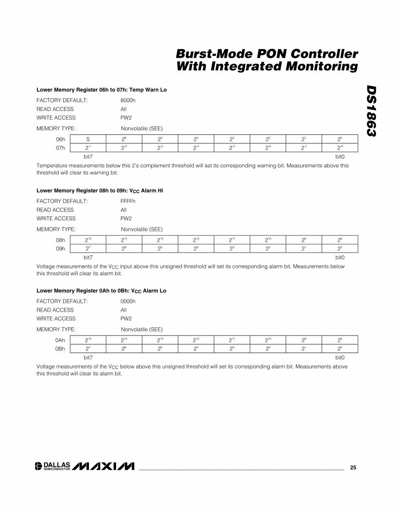
Lower Memory Register 06h to 07h: Temp Warn Lo
FACTORY DEFAULT: 8000h
READ ACCESS All
WRITE ACCESS PW2
MEMORY TYPE: Nonvolatile (SEE)
06h S 26 25 24 23 22 21 20
07h 2-1 2-2 2-3 2-4 2-5 2-6 2-7 2-8
bit7 bit0
Temperature measurements below this 2’s complement threshold will set its corresponding warning bit. Measurements above thisthreshold will clear its warning bit.
Lower Memory Register 08h to 09h: VCC Alarm Hi
FACTORY DEFAULT: FFFFh
READ ACCESS All
WRITE ACCESS PW2
MEMORY TYPE: Nonvolatile (SEE)
08h 215 214 213 212 211 210 29 28
09h 27 26 25 24 23 22 21 20
bit7 bit0
Voltage measurements of the VCC input above this unsigned threshold will set its corresponding alarm bit. Measurements belowthis threshold will clear its alarm bit.
Lower Memory Register 0Ah to 0Bh: VCC Alarm Lo
FACTORY DEFAULT: 0000h
READ ACCESS All
WRITE ACCESS PW2
MEMORY TYPE: Nonvolatile (SEE)
0Ah 215 214 213 212 211 210 29 28
0Bh 27 26 25 24 23 22 21 20
bit7 bit0
Voltage measurements of the VCC below above this unsigned threshold will set its corresponding alarm bit. Measurements abovethis threshold will clear its alarm bit.

DS
18
63
Burst-Mode PON ControllerWith Integrated Monitoring
26 ____________________________________________________________________
Lower Memory Register 0Eh to 0Fh: VCC Warn Lo
FACTORY DEFAULT: 0000h
READ ACCESS All
WRITE ACCESS PW2
MEMORY TYPE: Nonvolatile (SEE)
0Eh 215 214 213 212 211 210 29 28
0Fh 27 26 25 24 23 22 21 20
bit7 bit0
V ol tag e m easur em ents of the V C C b el ow ab ove thi s unsi g ned thr eshol d w i l l set i ts cor r esp ond i ng w ar ni ng b i t. M easur em ents ab ovethi s thr eshol d w i l l cl ear i ts w ar ni ng b i t.
Lower Memory Register 10h to 11h: MON1 Alarm Hi
FACTORY DEFAULT: FFFFh
READ ACCESS All
WRITE ACCESS PW2
MEMORY TYPE: Nonvolatile (SEE)
10h 215 214 213 212 211 210 29 28
11h 27 26 25 24 23 22 21 20
bit7 bit0
Voltage measurements of the MON1 input above this unsigned threshold will set its corresponding alarm bit. Measurements belowthis threshold will clear its alarm bit.
Lower Memory Register 0Ch to 0Dh: VCC Alarm Hi
FACTORY DEFAULT: FFFFh
READ ACCESS All
WRITE ACCESS PW2
MEMORY TYPE: Nonvolatile (SEE)
0Ch 215 214 213 212 211 210 29 28
0Dh 27 26 25 24 23 22 21 20
bit7 bit0
Voltage measurements of the VCC input above this unsigned threshold will set its corresponding warning bit. Measurements belowthis threshold will clear its warning bit.

DS
18
63
Burst-Mode PON ControllerWith Integrated Monitoring
____________________________________________________________________ 27
Lower Memory Register 12h to 13h: MON1 Alarm Lo
FACTORY DEFAULT: 0000h
READ ACCESS All
WRITE ACCESS PW2
MEMORY TYPE: Nonvolatile (SEE)
12h 215 214 213 212 211 210 29 28
13h 27 26 25 24 23 22 21 20
bit7 bit0
Voltage measurements of the MON1 input below this unsigned threshold will set its corresponding alarm bit. Measurements abovethis threshold will clear its alarm bit.
Lower Memory Register 14h to 15h: MON1 Warn Hi
FACTORY DEFAULT: FFFFh
READ ACCESS All
WRITE ACCESS PW2
MEMORY TYPE: Nonvolatile (SEE)
14h 215 214 213 212 211 210 29 28
15h 27 26 25 24 23 22 21 20
bit7 bit0
Voltage measurements of the MON1 input above this unsigned threshold will set its corresponding warning bit. Measurementsbelow this threshold will clear its warning bit.
Lower Memory Register 16h to 17h: MON1 Warn Lo
FACTORY DEFAULT: 0000h
READ ACCESS All
WRITE ACCESS PW2
MEMORY TYPE: Nonvolatile (SEE)
16h 215 214 213 212 211 210 29 28
17h 27 26 25 24 23 22 21 20
bit7 bit0
Voltage measurements of the MON1 input below this unsigned threshold will set its corresponding warning bit. Measurementsabove this threshold will clear its warning bit.

DS
18
63
Burst-Mode PON ControllerWith Integrated Monitoring
28 ____________________________________________________________________
Lower Memory Register 18h to 19h: MON2 Alarm Hi
FACTORY DEFAULT: FFFFh
READ ACCESS All
WRITE ACCESS PW2
MEMORY TYPE: Nonvolatile (SEE)
18h 215 214 213 212 211 210 29 28
19h 27 26 25 24 23 22 21 20
bit7 bit0
Voltage measurements of the MON2 input above this unsigned threshold will set its corresponding alarm bit. Measurements belowthis threshold will clear its alarm bit.
Lower Memory Register 1Ah to 1Bh: MON2 Alarm Lo
FACTORY DEFAULT: 0000h
READ ACCESS All
WRITE ACCESS PW2
MEMORY TYPE: Nonvolatile (SEE)
1Ah 215 214 213 212 211 210 29 28
1Bh 27 26 25 24 23 22 21 20
bit7 bit0
Voltage measurements of the MON2 input below this unsigned threshold will set its corresponding alarm bit. Measurements abovethis threshold will clear its alarm bit.
Lower Memory Register 1Ch to 1Dh: MON2 Alarm Hi
FACTORY DEFAULT: FFFFh
READ ACCESS All
WRITE ACCESS PW2
MEMORY TYPE: Nonvolatile (SEE)
1Ch 215 214 213 212 211 210 29 28
1Dh 27 26 25 24 23 22 21 20
bit7 bit0
Voltage measurements of the MON2 input above this unsigned threshold will set its corresponding warning bit. Measurementsbelow this threshold will clear its warning bit.

DS
18
63
Burst-Mode PON ControllerWith Integrated Monitoring
____________________________________________________________________ 29
Lower Memory Register 1Eh to 1Fh: MON2 Warn Lo
FACTORY DEFAULT: 0000h
READ ACCESS All
WRITE ACCESS PW2
MEMORY TYPE: Nonvolatile (SEE)
1Eh 215 214 213 212 211 210 29 28
1Fh 27 26 25 24 23 22 21 20
bit7 bit0
Voltage measurements of the MON2 input below this unsigned threshold will set its corresponding warning bit. Measurementsabove this threshold will clear its warning bit.
Lower Memory Register 20h to 21h: MON3 Alarm Hi
FACTORY DEFAULT: FFFFh
READ ACCESS All
WRITE ACCESS PW2
MEMORY TYPE: Nonvolatile (SEE)
20h 215 214 213 212 211 210 29 28
21h 27 26 25 24 23 22 21 20
bit7 bit0
Voltage measurements of the MON3 input above this unsigned threshold will set its corresponding alarm bit. Measurements belowthis threshold will clear its alarm bit.
Lower Memory Register 22h to 23h: MON3 Alarm Lo
FACTORY DEFAULT: 0000h
READ ACCESS All
WRITE ACCESS PW2
MEMORY TYPE: Nonvolatile (SEE)
22h 215 214 213 212 211 210 29 28
23h 27 26 25 24 23 22 21 20
bit7 bit0
Voltage measurements of the MON3 input below this unsigned threshold will set its corresponding alarm bit. Measurements abovethis threshold will clear its alarm bit.

DS
18
63
Burst-Mode PON ControllerWith Integrated Monitoring
30 ____________________________________________________________________
Lower Memory Register 24h to 25h: MON3 Warn Hi
FACTORY DEFAULT: FFFFh
READ ACCESS All
WRITE ACCESS PW2
MEMORY TYPE: Nonvolatile (SEE)
24h 215 214 213 212 211 210 29 28
25h 27 26 25 24 23 22 21 20
bit7 bit0
Voltage measurements of the MON3 input above this unsigned threshold will set its corresponding warning bit. Measurementsbelow this threshold will clear its warning bit.
Lower Memory Register 26h to 27h: MON3 Warn Lo
FACTORY DEFAULT: 0000h
READ ACCESS All
WRITE ACCESS PW2
MEMORY TYPE: Nonvolatile (SEE)
26h 215 214 213 212 211 210 29 28
27h 27 26 25 24 23 22 21 20
bit7 bit0
Voltage measurements of the MON3 input below this unsigned threshold will set its corresponding warning bit. Measurementsabove this threshold will clear its warning bit.
Lower Memory Register 28h to 2Fh: Shadowed EEPROM
FACTORY DEFAULT: 00h
READ ACCESS All
WRITE ACCESS PW2
MEMORY TYPE: Nonvolatile (SEE)
28h-2Fh SEE SEE SEE SEE SEE SEE SEE SEE
bit7 bit0
Shadowed EEPROM memory (see details in Memory Map section). PW2 level access controlled ROM data for end user.

DS
18
63
Burst-Mode PON ControllerWith Integrated Monitoring
____________________________________________________________________ 31
Lower Memory Register 30h to 5Fh: PW2 EE
FACTORY DEFAULT: 00h
READ ACCESS All
WRITE ACCESS PW2
MEMORY TYPE: Nonvolatile (EE)
30h-5Fh EE EE EE EE EE EE EE EE
bit7 bit0
Nonvolatile EEPROM memory. PW2 level access controlled ROM data for end user.
Lower Memory Register 60h to 61h: Temp Value
POWER-ON VALUE 0000h
READ ACCESS All
WRITE ACCESS N/A
MEMORY TYPE: Volatile
60h S 26 25 24 23 22 21 20
61h 2-1 2-2 2-3 2-4 2-5 2-6 2-7 2-8
bit7 bit0
Signed 2’s complement Direct-to-Temperature measurement.
Lower Memory, Register 62h–63h: VCC ValueLower Memory, Register 64h–65h: MON1 ValueLower Memory, Register 66h–67h: MON2 ValueLower Memory, Register 68h–69h: MON3 Value
POWER-ON VALUE 0000h
READ ACCESS All
WRITE ACCESS N/A
MEMORY TYPE: Volatile
62h 215 214 213 212 211 210 29 28
63h 27 26 25 24 23 22 21 20
64h 215 214 213 212 211 210 29 28
65h 27 26 25 24 23 22 21 20
66h 215 214 213 212 211 210 29 28
67h 27 26 25 24 23 22 21 20
68h 215 214 213 212 211 210 29 28
69h 27 26 25 24 23 22 21 20
bit7 bit0
Unsigned voltage measurement.

DS
18
63
Burst-Mode PON ControllerWith Integrated Monitoring
32 ____________________________________________________________________
Lower Memory, Register 6Ah to 6D: Reserved
POWER-ON VALUE 00h
READ ACCESS All
WRITE ACCESS N/A
MEMORY TYPE
These registers are reserved. The value when read is 00h.
Lower Memory, Register 6Eh: Status
POWER-ON VALUE x000 0x0x b
READ ACCESS All
WRITE ACCESS See Below
MEMORY TYPE Volatile
WriteAccess N/A All N/A All All N/A N/A N/A
6EhFETG
STATUSSOFTFETG
RESERVEDTX-F
RESETSOFTTX-D
TX-FSTATUS
RESERVED RDYB
bit7 bit0
bit7FETG STATUS: Reflects the active state of FETG.0 = Bias and modulation outputs are enabled.1 = The FETG output is asserted to disable the bias and modulation outputs.
bit6SOFT FETG:0 = (Default)1 = Force the bias and modulation outputs to their off states and asserts the FETG output.
bit5 Reserved (Default = 0)
bit4
TX-F RESET:0 = Does not affect the TX-F output (Default).
1 = Resets the latch for the TX-F output.This bit is self clearing after the reset.
bit3
SOFT TX-D: This bit allows a software control that is identical to the TX-D pin. Please see section onTX-D for further information. It’s value is wired OR’ed with the logic value on TX-D pin.0 = Internal TX-D signal is equal to external TX-D pin.1 = Internal TX-D signal is high.
bit2
TX-F STATUS: Reflects the active state of TX-F.
0 = TX-F pin is not active.1 = TX-F pin is active.
bit1 RESERVED (Default = 0)
bit0
RDYB: Ready Bar.
0 = VCC is above POA.
1 = VCC is below POA or too low to communicate over the I2C bus.

DS
18
63
Burst-Mode PON ControllerWith Integrated Monitoring
____________________________________________________________________ 33
Lower Memory, Register 6Fh: Update
POWER-ON VALUE 00h
READ ACCESS All
WRITE ACCESS All + DS1863 Hardware
MEMORY TYPE Volatile
6Fh TEMP RDY VCC RDY MON1 RDY MON2 RDY MON3 RDY RESERVED RESERVED RESERVED
bit7 bit0
Status of completed conversions. At Power-On, these bits are cleared and will be set as each conversion is completed. These bitscan be cleared so that a completion of a new conversion is verified.
bit7
TEMP RDY:0 = Temperature conversion is not ready (Default).
1 = Temperature conversion is ready.
bit6
VCC RDY:
0 = VCC conversion is not ready (Default).
1 = VCC conversion is ready.
bit5
MON1 RDY:0 = MON1 conversion is not ready (Default).1 = MON1 conversion is ready.
bit4
MON2 RDY:0 = MON2 conversion is not ready (Default).1 = MON2 conversion is ready.
bit3
MON3 RDY:0 = MON3 conversion is not ready (Default).
1 = MON3 conversion is ready.
bit2:0 RESERVED

DS
18
63
Burst-Mode PON ControllerWith Integrated Monitoring
34 ____________________________________________________________________
Lower Memory, Register 70h: Alarm3
POWER-ON VALUE 10h
READ ACCESS All
WRITE ACCESS N/A
MEMORY TYPE Volatile
70h TEMP HI TEMP LO VCC HI VCC LO MON1 HI MON1 LO MON2 HI MON2 LO
bit7 bit0
Alarm Status Bits
bit7
TEMP HI: High Alarm Status for Temperature measurement.0 = (Default) Last measurement was equal to or below threshold setting.
1 = Last measurement was above threshold setting.
bit6TEMP LO: Low Alarm Status for Temperature measurement.0 = (Default) Last measurement was equal to or above threshold setting.1 = Last measurement was below threshold setting.
bit5
VCC HI: High Alarm Status for VCC measurement.
0 = (Default) Last measurement was equal to or below threshold setting.
1 = Last measurement was above threshold setting.
bit4
VCC LO: Low Alarm Status for VCC measurement. This bit is set when the VCC supply is below thePOA trip point value. It will clear itself when a VCC measurement is completed and the value is abovethe low threshold.0 = Last measurement was equal to or above threshold setting.1 = (Default) Last measurement was below threshold setting.
bit3
MON1 HI: High Alarm Status for MON1 measurement.0 = (Default) Last measurement was equal to or below threshold setting.
1 = Last measurement was above threshold setting.
bit2
MON1 LO: Low Alarm Status for MON1 measurement.0 = (Default) Last measurement was equal to or above threshold setting.1 = Last measurement was below threshold setting.
bit1
MON2 HI: High Alarm Status for MON2 measurement.0 = (Default) Last measurement was equal to or below threshold setting.
1 = Last measurement was above threshold setting.
bit0
MON2 LO: Low Alarm Status for MON2 measurement.0 = (Default) Last measurement was equal to or above threshold setting.1 = Last measurement was below threshold setting.

DS
18
63
Burst-Mode PON ControllerWith Integrated Monitoring
____________________________________________________________________ 35
Lower Memory, Register 71h: Alarm2
POWER-ON VALUE 00h
READ ACCESS All
WRITE ACCESS N/A
MEMORY TYPE Volatile
71h MON3 HI MON3 LO RESERVED RESERVED RESERVED RESERVED RESERVED RESERVED
bit7 bit0
Alarm Status Bits
bit7
MON3 HI: High Alarm Status for MON3 measurement.0 = (Default) Last measurement was equal to or below threshold setting.
1 = Last measurement was above threshold setting.
bit6MON3 LO: Low Alarm Status for MON3 measurement.0 = (Default) Last measurement was equal to or above threshold setting.1 = Last measurement was below threshold setting.
bit5:0 RESERVED

DS
18
63
Burst-Mode PON ControllerWith Integrated Monitoring
36 ____________________________________________________________________
Lower Memory, Register 72h: Alarm1
POWER-ON VALUE 00h
READ ACCESS All
WRITE ACCESS N/A
MEMORY TYPE Volatile
72h RESERVED RESERVED RESERVED RESERVED BIAS HI RESERVED TX-P HI TX-P LO
bit7 bit0
Alarm Status Bits
bit7:4 RESERVED
bit3BIAS HI: High Alarm Status Bias; Fast Comparison.
0 = (Default) Last measurement was equal to or below threshold setting.1 = Last measurement was above threshold setting.
bit2 RESERVED
bit1TX-P HI: High Alarm Status TX-P; Fast Comparison.0 = (Default) Last measurement was equal to or below threshold setting.1 = Last measurement was above threshold setting.
bit0
TX-P LO: Low Alarm Status TX-P; Fast Comparison.0 = Last measurement was equal to or above threshold setting.
1 = Last measurement was below threshold setting.
Lower Memory, Register 73h: Alarm0
POWER-ON VALUE 00h
READ ACCESS All
WRITE ACCESS N/A
MEMORY TYPE Volatile
73h RESERVED RESERVED RESERVED RESERVED BIAS MAX RESERVED RESERVED RESERVED
bit7 bit0
Alarm Status Bits
bit7:4 RESERVED
bit3 BIAS MAX: Maximum digital setting for IBIAS.
0 = (Default) The value of IBIAS is equal to or below MAX IBIAS setting.1 = Requested value of IBIAS is greater than MAX IBIAS setting.
bit2:0 RESERVED

DS
18
63
Burst-Mode PON ControllerWith Integrated Monitoring
____________________________________________________________________ 37
Lower Memory, Register 74h: Warn3
POWER-ON VALUE 10h
READ ACCESS All
WRITE ACCESS N/A
MEMORY TYPE Volatile
74h TEMP HI TEMP LO VCC HI VCC LO MON1 HI MON1 LO MON2 HI MON2 LO
bit7 bit0
Warning Status Bits
bit7 TEMP HI: High Warning Status for Temperature measurement.0 = (Default) Last measurement was equal to or below threshold setting.
1 = Last measurement was above threshold setting.
bit6 TEMP LO: Low Warning Status for Temperature measurement.
0 = (Default) Last measurement was equal to or above threshold setting.1 = Last measurement was below threshold setting.
bit5 VCC HI: High Warning Status for VCC measurement.
0 = (Default) Last measurement was equal to or below threshold setting.
1 = Last measurement was above threshold setting.
bit4 VCC LO: Low Warning Status for VCC measurement. This bit is set when the VCC supply is below thePOA trip point value. It will clear itself when a VCC measurement is completed and the value is abovethe low threshold.
0 = Last measurement was equal to or above threshold setting.1 = (Default) Last measurement was below threshold setting.
bit3 MON1 HI: High Warning Status for MON1 measurement.0 = (Default) Last measurement was equal to or below threshold setting.1 = Last measurement was above threshold setting.
bit2 MON1 LO: Low Warning Status for MON1 measurement.
0 = (Default) Last measurement was equal to or above threshold setting.1 = Last measurement was below threshold setting.
bit1 MON2 HI: High Warning Status for MON2 measurement.0 = (Default) Last measurement was equal to or below threshold setting.
1 = Last measurement was above threshold setting.
bit0 MON2 LO: Low Warning Status for MON2 measurement.0 = (Default) Last measurement was equal to or above threshold setting.1 = Last measurement was below threshold setting.

DS
18
63
Burst-Mode PON ControllerWith Integrated Monitoring
38 ____________________________________________________________________
Lower Memory, Register 75h: Warn2
POWER-ON VALUE 10h
READ ACCESS All
WRITE ACCESS N/A
MEMORY TYPE Volatile
75h MON3 HI MON3 LO RESERVED RESERVED RESERVED RESERVED RESERVED RESERVED
bit7 bit0
Warning Status Bits
bit7 MON3 HI: High Warning Status for Mon3 measurement.0 = (Default) Last measurement was equal to or below threshold setting.
1 = Last measurement was above threshold setting.
bit6 MON3 LO: Low Warning Status for Mon3 measurement.0 = (Default) Last measurement was equal to or above threshold setting.1 = Last measurement was below threshold setting.
bit5 RESERVED
Lower Memory, Register 76h to 7Ah: Reserved
POWER-ON VALUE 00h
READ ACCESS All
WRITE ACCESS N/A
MEMORY TYPE
These registers are reserved. The value when read is 00h.
Lower Memory, Register 7Bh to 7Eh: Password Entry (PWE)
FACTORY DEFAULT FFFF FFFFh
READ ACCESS N/A
WRITE ACCESS All
MEMORY TYPE Volatile
7Bh 231 230 229 228 227 226 225 224
7Ch 223 222 221 220 219 218 217 216
7Dh 215 214 213 212 211 210 29 28
7Eh 27 26 25 24 23 22 21 20
bit7 bit0
Password Entry. There are two passwords for the DS1863. Each password is 4 bytes long. The lower level password (PW1) willhave all the access of a normal user plus those made available with PW1. The higher level password (PW2) will have all of theaccess of PW1 plus those made available with PW2. The values of the passwords reside in EE inside of PW2 memory. At Power upall PWE bits are set to 1. All reads to this location are 0.

DS
18
63
Burst-Mode PON ControllerWith Integrated Monitoring
____________________________________________________________________ 39
Lower Memory Register 7Fh: Table Select (TBL SEL)
POWER-ON VALUE 00h
READ ACCESS All
WRITE ACCESS All
MEMORY TYPE Volatile
7Fh 27 26 25 24 23 22 21 20
bit7 bit0
The upper memory tables (Table 01h–Table 05h) of the DS1863 are accessible by writing the correct table value in this register.

DS
18
63
Burst-Mode PON ControllerWith Integrated Monitoring
40 ____________________________________________________________________
Table 01h, Register F8h: Alarm3
POWER-ON VALUE 00h
READ ACCESS All
WRITE ACCESS PW1
MEMORY TYPE Volatile
F8h TEMP HI TEMP LO VCC HI VCC LO MON1 HI MON1 LO MON2 HI MON2 LO
bit7 bit0
Layout is identical to Alarm3 in Lower Memory Register 70h with two exceptions.1. VCC Low alarm is not set at power-on.2. These bits are latched. They are cleared by power-down or a write with PW1 access.
Table 01h, Register 80h to F7h: PW1 EEPROM
POWER-ON VALUE 00h
READ ACCESS PW1
WRITE ACCESS PW1
MEMORY TYPE Nonvolatile(EE)
80h-F7h EE EE EE EE EE EE EE EE
bit7 bit0
EEPROM for PW1 level access.
Table 01h, Registers
Table 01h, Register F9h: Alarm2
POWER-ON VALUE 00h
READ ACCESS All
WRITE ACCESS PW1
MEMORY TYPE Volatile
F9h MON3 HI MON3 LO RESERVED RESERVED RESERVED RESERVED RESERVED RESERVED
bit7 bit0
Layout is identical to Alarm2 in Lower Memory Register 71h with one exception.1. These bits are latched. They are cleared by power-down or a write with PW1 access.

DS
18
63
Burst-Mode PON ControllerWith Integrated Monitoring
____________________________________________________________________ 41
Table 01h, Register FBh: Alarm0
POWER-ON VALUE 00h
READ ACCESS All
WRITE ACCESS PW1
MEMORY TYPE Volatile
72h RESERVED RESERVED RESERVED RESERVED BIAS MAX RESERVED RESERVED RESERVED
bit7 bit0
Layout is identical to Alarm0 in Lower Memory Register 73h with one exception.1. These bits are latched. They are cleared by power-down or a write with PW1 access
Table 01h, Register FAh: Alarm1
POWER-ON VALUE 00h
READ ACCESS All
WRITE ACCESS PW1
MEMORY TYPE Volatile
FAh BIAS HI TX-P HI TX-P LO RESERVED RESERVED RESERVED RESERVED RESERVED
bit7 bit0
Layout is identical to Alarm1 in Lower Memory Register 72h with one exception.1. These bits are latched. They are cleared by power-down or a write with PW1 access.
Table 01h, Register FCh: Warn3
POWER-ON VALUE 00h
READ ACCESS All
WRITE ACCESS PW1
MEMORY TYPE Volatile
FCh TEMP HI TEMP LO VCC HI VCC LO MON1 HI MON1 LO MON2 HI MON2 LO
bit7 bit0
Layout is identical to Warn3 in Lower Memory Register 74h with two exceptions.1. VCC Low Warning is not set at power-on.2. These bits are latched. They are cleared by power-down or a write with PW1 access.

DS
18
63
Burst-Mode PON ControllerWith Integrated Monitoring
42 ____________________________________________________________________
Table 01h, Register FDh: Warn2
POWER-ON VALUE 00h
READ ACCESS All
WRITE ACCESS PW1
MEMORY TYPE Volatile
FDh MON3 HI MON3 LO RESERVED RESERVED RESERVED RESERVED RESERVED RESERVED
bit7 bit0
Layout is identical to Warn2 in Lower Memory Register 75h with one exception.1. These bits are latched. They are cleared by power-down or a write with PW1 access.
Table 01h, Register FEh to FFh: Reserved
POWER-ON VALUE 00h
READ ACCESS All
WRITE ACCESS PW1
MEMORY TYPE Volatile
These registers are reserved.

DS
18
63
Burst-Mode PON ControllerWith Integrated Monitoring
____________________________________________________________________ 43
Table 02h, Register 80h: Mode
POWER-ON VALUE 0Fh
READ ACCESS PW2
WRITE ACCESS PW2
MEMORY TYPE Volatile
80h SEEB RESERVED RESERVED RESERVED AEN MOD-EN APC-EN BIAS-EN
bit7 bit0
bit7
SEEB:0 = Enables EEPROM writes to SEE bytes in Table 02h (Default).1 = Disables EEPROM writes to SEE bytes during configuration, so that the configuration of the part isnot delayed by the EE cycle time. Once the values are known, write this bit to a 0 and write the SEElocations again for data to be written to the EEPROM.
bit6:4 RESERVED
bit3
AEN:0 = The temperature calculated index value (‘T Index’) is write-able by the user and the updates ofcalculated indexes are disabled. This allows the user to interactively test their modules by controllingthe indexing for the look-up tables. The recalled values from the LUTs will appear in the DAC registersafter the next completion of a temperature conversion (just like it would happen is auto mode). BothDACs will update at the same time (just like auto mode).1 = Enables auto control of the LUT (Default).
bit2
MOD-EN:0 = “MOD DAC” is write-able by the user and the LUT recalls are disabled. This allows the user tointeractively test their modules by writing the DAC value for modulation. The output is updated withthe new value at the end of the write cycle. The I_C Stop condition is the end of the write cycle.1 = Enables auto control of the LUT for modulation (Default).
bit1
APC-EN:0 = “APC DAC” is write-able by the user and the LUT recalls are disabled. This allows the user tointeractively test their modules by writing the DAC value for APC reference. The output is updatedwith the new value at the end of the write cycle. The I_C Stop condition is the end of the write cycle.1 = Enables auto control of the LUT for APC reference (Default).
bit0
BIAS-EN:0 = “BIAS DAC” is controlled by the user and the APC is open loop. The “BIAS DAC” value is writtento the “MAN IBIAS” Register. All values that are written to “MAN IBIAS” and are greater than the “MAXIBIAS” register setting are not updated and will set the “BIAS MAX” alarm bit. The “BIAS DAC”register will continue to reflect the value of the Bias DAC. This allows the user to interactively test theirmodules by writing the DAC value for bias. The output is updated with the new value at the end of thewrite cycle to the “MAN IBIAS” register. The I2C Stop condition is the end of the write cycle.
1 = Enables auto control for the APC feedback (Default).
Table 02h, Registers
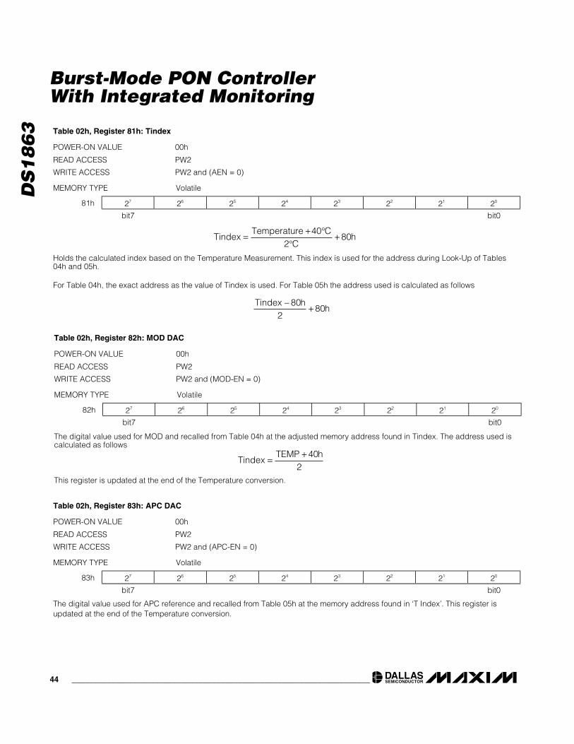
DS
18
63
Burst-Mode PON ControllerWith Integrated Monitoring
44 ____________________________________________________________________
Table 02h, Register 81h: Tindex
POWER-ON VALUE 00h
READ ACCESS PW2
WRITE ACCESS PW2 and (AEN = 0)
MEMORY TYPE Volatile
81h 27 26 25 24 23 22 21 20
bit7 bit0
Holds the calculated index based on the Temperature Measurement. This index is used for the address during Look-Up of Tables04h and 05h.
For Table 04h, the exact address as the value of Tindex is used. For Table 05h the address used is calculated as follows
Table 02h, Register 82h: MOD DAC
POWER-ON VALUE 00h
READ ACCESS PW2
WRITE ACCESS PW2 and (MOD-EN = 0)
MEMORY TYPE Volatile
82h 27 26 25 24 23 22 21 20
bit7 bit0
The digital value used for MOD and recalled from Table 04h at the adjusted memory address found in Tindex. The address used iscalculated as follows
This register is updated at the end of the Temperature conversion.
Tindex hh
−+
802
80
TindexTemperature C
Ch=
+ °°
+40
280
Tindex =+TEMP h40
2
Table 02h, Register 83h: APC DAC
POWER-ON VALUE 00h
READ ACCESS PW2
WRITE ACCESS PW2 and (APC-EN = 0)
MEMORY TYPE Volatile
83h 27 26 25 24 23 22 21 20
bit7 bit0
The digital value used for APC reference and recalled from Table 05h at the memory address found in ‘T Index’. This register isupdated at the end of the Temperature conversion.
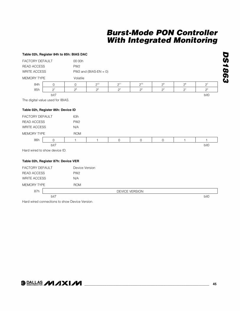
DS
18
63
Burst-Mode PON ControllerWith Integrated Monitoring
____________________________________________________________________ 45
Table 02h, Register 84h to 85h: BIAS DAC
FACTORY DEFAULT 00 00h
READ ACCESS PW2
WRITE ACCESS PW2 and (BIAS-EN = 0)
MEMORY TYPE Volatile
84h 0 0 212 211 210 29 28 27
85h 27 26 25 24 23 22 21 20
bit7 bit0
The digital value used for IBIAS.
Table 02h, Register 86h: Device ID
FACTORY DEFAULT 63h
READ ACCESS PW2
WRITE ACCESS N/A
MEMORY TYPE ROM
86h 0 1 1 0 0 0 1 1
bit7 bit0
Hard wired to show device ID.
Table 02h, Register 87h: Device VER
FACTORY DEFAULT Device Version
READ ACCESS PW2
WRITE ACCESS N/A
MEMORY TYPE ROM
87h DEVICE VERSION
bit7 bit0
Hard wired connections to show Device Version.

DS
18
63
Burst-Mode PON ControllerWith Integrated Monitoring
46 ____________________________________________________________________
Table 02h, Register 88h: Update Rate
FACTORY DEFAULT 00h
READ ACCESS PW2
WRITE ACCESS PW2
MEMORY TYPE Nonvolatile (SEE)
Defines the update rate for comparison of APC control.
88h 0 0 0 0 SR(3:0)
bit7 bit0
bit7:4 0
bit3:0 SR(3:0) : 4-bit update rate for comparison of APC control.
SR3–SR0
MINIMUM TIMEFROM BEN TO FIRST
SAMPLE (tFIRST)±50ns
REPEATED SAMPLEPERIOD FOLLOWINGFIRST SAMPLE (tREP)
0000b 350ns 800ns
0001b 550ns 1200ns
0010b 750ns 1600ns
0011b 950ns 2000ns
0100b 1350ns 2800ns
0101b 1550ns 3200ns
0110b 1750ns 3600ns
0111b 2150ns 4400ns
1000b 2950ns 6000ns
1001b* 3150ns 6400ns
*All codes greater than 1001b (1010b–111b) use the maximumsample time of code 1001b.

DS
18
63
Burst-Mode PON ControllerWith Integrated Monitoring
____________________________________________________________________ 47
Table 02h, Register 8Ah: Startup Step
FACTORY DEFAULT: 00h
READ ACCESS PW2
WRITE ACCESS PW2
MEMORY TYPE: Nonvolatile (SEE)
8Ah 212 211 210 29 28 27 26 25
bit7 bit0
This value will define the maximum allowed step for the upper 8 bits of IBIAS output during start-up.
Table 02h, Register 89h: Config
FACTORY DEFAULT 00h
READ ACCESS PW2
WRITE ACCESS PW2
MEMORY TYPE Nonvolatile (SEE)
89h FE TG D IR TX - F E N RE S E RV E D AS E L RE S E RV E D RE S E RV E D RE S E RV E D RE S E RV E D
bit7 bit0
Configure the memory location and the polarity of the digital outputs.
bit7
FETG DIR: Chooses the direction or polarity of the FETG output for normal operation.
0 = Under normal operation, FETG will be pulled low. (Default)1 = Under normal operation, FETG will be pulled high.
bit6
TX-F EN:0 = The alarm bits will immediately reflect the status of the last comparison. (Default)
1 = The alarm bits are latched until cleared by a TX-D transition or Power-down. If VCC low alarm isenabled for either FETG or TX-F then latching is disabled until after the first VCC measurement ismade above the VCC to set-point to allow for proper operation during slow power-on cycles.
bit5 RESERVED
bit4
ASEL: Address SELect.0 = Device Address of A2h (Default).1 = Device-Address is equal to the value found in byte ‘device_address’ (Table 02h, 8Ch).
bit3:0 RESERVED
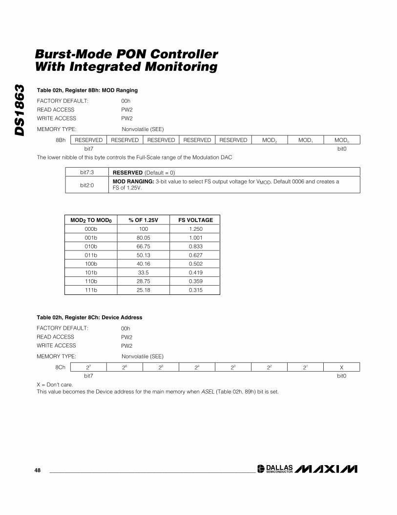
DS
18
63
Burst-Mode PON ControllerWith Integrated Monitoring
48 ____________________________________________________________________
Table 02h, Register 8Bh: MOD Ranging
FACTORY DEFAULT: 00h
READ ACCESS PW2
WRITE ACCESS PW2
MEMORY TYPE: Nonvolatile (SEE)
8Bh RESERVED RESERVED RESERVED RESERVED RESERVED MOD2 MOD1 MOD0
bit7 bit0
The lower nibble of this byte controls the Full-Scale range of the Modulation DAC
bit7:3 RESERVED (Default = 0)
bit2:0MOD RANGING: 3-bit value to select FS output voltage for VMOD. Default 0006 and creates aFS of 1.25V.
Table 02h, Register 8Ch: Device Address
FACTORY DEFAULT: 00h
READ ACCESS PW2
WRITE ACCESS PW2
MEMORY TYPE: Nonvolatile (SEE)
8Ch 27 26 25 24 23 22 21 X
bit7 bit0
X = Don't care.This value becomes the Device address for the main memory when ASEL (Table 02h, 89h) bit is set.
MOD2 TO MOD0 % OF 1.25V FS VOLTAGE
000b 100 1.250
001b 80.05 1.001
010b 66.75 0.833
011b 50.13 0.627
100b 40.16 0.502
101b 33.5 0.419
110b 28.75 0.359
111b 25.18 0.315

DS
18
63
Burst-Mode PON ControllerWith Integrated Monitoring
____________________________________________________________________ 49
Table 02h, Register 8Dh: Comp Ranging
FACTORY DEFAULT: 00h
READ ACCESS PW2
WRITE ACCESS PW2
MEMORY TYPE: Nonvolatile (SEE)
8Dh RESERVED RESERVED RESERVED RESERVED RESERVED APC2 APC1 APC0
bit7 bit0
This byte controls the Full-Scale range for the Quick-Trip monitoring of the APC reference as well as the closed loop monitoring ofAPC.
bit7:3 RESERVED (Default = 0)
bit2:0APC RANGING: 3-bit value to select the FS comparison voltage for BMD with the APC. Default is000b and creates a FS voltage of 2.5V.
Table 02h, Register 8Eh: Right Shift1
FACTORY DEFAULT: 00h
READ ACCESS PW2
WRITE ACCESS PW2
MEMORY TYPE: Nonvolatile (SEE)
8Eh RESERVED MON1_2 MON1_1 MON1_0 RESERVED MON2_2 MON2_1 MON2_0
bit7 bit0
Allows for right-shifting the final answer of MON1 and MON2 voltage measurements. This allows for scaling the measurements tothe smallest Full-scale voltage and then right-shifting the final result so the reading is weighted to the correct LSB.
APC2 TO APC0 % OF 2.5V FS VOLTAGE
000b 100 2.500
001b 80.07 2.002
010b 66.79 1.670
011b 50.18 1.255
100b 40.22 1.006
101b 33.57 0.839
110b 28.82 0.721
111b 25.26 0.632

DS
18
63
Burst-Mode PON ControllerWith Integrated Monitoring
50 ____________________________________________________________________
Table 02h, Register 8Fh: Right Shift0
FACTORY DEFAULT: 00h
READ ACCESS PW2
WRITE ACCESS PW2
MEMORY TYPE: Nonvolatile (SEE)
8Fh RESERVED MON3_2 MON3_1 MON3_0 RESERVED RESERVED RESERVED RESERVED
bit7 bit0
Allows for right-shifting the final answer of MON3 voltage measurements. This allows for scaling the measurements to the smallestfull-scale voltage and then right-shifting the final result so the reading is weighted to the correct LSB.
Table 02h, Register 90h to 91h: Reserved
FACTORY DEFAULT: 0000h
READ ACCESS PW2
WRITE ACCESS PW2
MEMORY TYPE: Nonvolatile (SEE)
These registers are reserved.
Table 02h, Register 92h to 93h: VCC Scale
FACTORY CALIBRATED
READ ACCESS PW2
WRITE ACCESS PW2
MEMORY TYPE Nonvolatile (SEE)
92h 215 214 213 212 211 210 29 28
93h 27 26 25 24 23 22 21 20
bit7 bit0
Controls the Scaling or Gain of the VCC measurements. The factory-calibrated value will produce a FS voltage of 6.5536V.

DS
18
63
Burst-Mode PON ControllerWith Integrated Monitoring
____________________________________________________________________ 51
Table 02h, Register 94h to 95h: MON1 ScaleTable 02h, Register 96h to 97h: MON2 ScaleTable 02h, Register 98h to 99h: MON3 Scale
FACTORY CALIBRATED
READ ACCESS PW2
WRITE ACCESS PW2
MEMORY TYPE Nonvolatile (SEE)
94h 215 214 213 212 211 210 29 28
95h 27 26 25 24 23 22 21 20
96h 215 214 213 212 211 210 29 28
97h 27 26 25 24 23 22 21 20
98h 215 214 213 212 211 210 29 28
99h 27 26 25 24 23 22 21 20
bit7 bit0
Controls the Scaling or Gain of the MON1, MON2, and MON3 measurements. The default hexadecimal value will correspond to2.5V. The factory-calibrated value will produce a FS voltage of 2.5V.
Table 02h, Register 9Ah to A1h: Reserved
FACTORY DEFAULT 0000h
READ ACCESS PW2
WRITE ACCESS PW2
MEMORY TYPE Nonvolatile (SEE)
These registers are reserved.
Table 02h, Register A2h to A3h: VCC Offset
FACTORY DEFAULT 0000h
READ ACCESS PW2
WRITE ACCESS PW2
MEMORY TYPE Nonvolatile (SEE)
A2h S S 215 214 213 212 211 210
A3h 29 28 27 26 25 24 23 22
bit7 bit0
Allows for offset control of VCC measurement if desired.

DS
18
63
Burst-Mode PON ControllerWith Integrated Monitoring
52 ____________________________________________________________________
Table 02h, Register A4h to A5h: MON1 OffsetTable 02h, Register A6h to A7h: MON2 OffsetTable 02h, Register A8h to A9h: MON3 Offset
FACTORY DEFAULT 0000h
READ ACCESS PW2
WRITE ACCESS PW2
MEMORY TYPE Nonvolatile (SEE)
A4h S S 215 214 213 212 211 210
A5h 29 28 27 26 25 24 23 22
A6h S S 215 214 213 212 211 210
A7h 29 28 27 26 25 24 23 22
A8h S S 215 214 213 212 211 210
A9h 29 28 27 26 25 24 23 22
bit7 bit0
Allows for offset control of MON1, MON2, and MON3 measurement if desired.
Table 02h, Register AAh to ADh: Reserved
FACTORY DEFAULT 0000 0000h
READ ACCESS PW2
WRITE ACCESS PW2
MEMORY TYPE Nonvolatile (SEE)
These registers are reserved.
Table 02h, Register AEh to AFh: Temp Offset
FACTORY CALIBRATED
READ ACCESS PW2
WRITE ACCESS PW2
MEMORY TYPE Nonvolatile (SEE)
AEh S 28 27 26 25 24 23 22
AFh 21 20 2-1 2-2 2-3 2-4 2-5 2-6
bit7 bit0
Allows for offset control of Temp measurement if desired. The Final Result must be XOR’ed with BB40h before writing to thisregister. Factory calibration contains the desired value for a reading of the temperature in degrees celcius.

DS
18
63
Burst-Mode PON ControllerWith Integrated Monitoring
____________________________________________________________________ 53
Table 02h, Register B0h to B3h: PW1
FACTORY DEFAULT FFFF FFFFh
READ ACCESS N/A
WRITE ACCESS PW2
MEMORY TYPE Nonvolatile (SEE)
B0h 231 230 229 228 227 226 225 224
B1h 223 222 221 220 219 218 217 216
B2h 215 214 213 212 211 210 29 28
B3h 27 26 25 24 23 22 21 20
bit7 bit0
The PWE value is compared against the value written to this location to enable PW1 access. At power-on, the PWE value is set to allones. Thus writing these bytes to all ones grants PW1 access on power-up without writing the password entry. All reads of thisregister are 00h.
Table 02h, Register B4h to B7h: PW2
FACTORY DEFAULT FFFF FFFFh
READ ACCESS N/A
WRITE ACCESS PW2
MEMORY TYPE Nonvolatile (SEE)
B4h 231 230 229 228 227 226 225 224
B5h 223 222 221 220 219 218 217 216
B6h 215 214 213 212 211 210 29 28
B7h 27 26 25 24 23 22 21 20
bit7 bit0
The PWE value is compared against the value written to this location to enable PW2 access. At power-on, the PWE value is set to allones. Thus writing these bytes to all ones grants PW2 access on power-up without writing the password entry. All reads of thisregister are 00h.

DS
18
63
Burst-Mode PON ControllerWith Integrated Monitoring
54 ____________________________________________________________________
Table 02h, Register B8h: FETG Enable1
FACTORY DEFAULT 00h
READ ACCESS PW2
WRITE ACCESS PW2
MEMORY TYPE Nonvolatile (SEE)
B8h TE M P E N V C C E N M ON 1 E N M ON 2 E N M ON 3 E N RE S E RV E D RE S E RV E D RE S E RV E D
bit7 bit0
Configures the maskable interrupt for the FETG pin.
bit7
TEMP EN: Enables/Disables active interrupts on the FETG pin due to temperature measurementsoutside the threshold limits.0 = Disable (Default)
1 = Enable
bit6
VCC EN: Enables/Disables active interrupts on the FETG pin due to VCC measurements outside thethreshold limits.0 = Disable (Default)1 = Enable
bit5
MON1 EN: Enables/Disables active interrupts on the FETG pin due to MON1 measurementsoutside the threshold limits.0 = Disable (Default)
1 = Enable
bit4
MON2 EN: Enables/Disables active interrupts on the FETG pin due to MON2 measurementsoutside the threshold limits.0 = Disable (Default)1 = Enable
bit3
MON3 EN: Enables/Disables active interrupts on the FETG pin due to MON3 measurementsoutside the threshold limits.0 = Disable (Default)1 = Enable
bit2:0 RESERVED (Default = 0)

DS
18
63
Burst-Mode PON ControllerWith Integrated Monitoring
____________________________________________________________________ 55
Table 02h, Register B9h: FETG Enable0
FACTORY DEFAULT 00h
READ ACCESS PW2
WRITE ACCESS PW2
MEMORY TYPE Nonvolatile (SEE)
B9h TX P - H I E N TX P - LO E N BIAS - H I E N BIAS M AX E N RE S E RV E D RE S E RV E D RE S E RV E D RE S E RV E D
bit7 bit0
Configures the maskable interrupt for the FETG pin.
bit7
TX-P-HI EN: Enables/Disables active interrupts on the FETG pin due to Tx-P fast comparisonsabove the threshold limit.0 = Disable (Default)
1 = Enable.
bit6
TX-P-LO EN: Enables/Disables active interrupts on the FETG pin due to Tx-P fast comparisonsbelow the threshold limit.0 = Disable (Default)1 = Enable
bit5
BIAS-HI EN: Enables/Disables active interrupts on the FETG pin due to BIAS fast comparisonsabove the threshold limit.0 = Disable (Default)1 = Enable
bit4
BIAS MAX EN: Enables/Disables active interrupts on the FETG pin due to BIAS fast comparisonsbelow the threshold limit.
0 = Disable (Default)1 = Enable
bit3:0 RESERVED (Default = 0)

DS
18
63
Burst-Mode PON ControllerWith Integrated Monitoring
56 ____________________________________________________________________
Table 02h, Register BAh: TX-F Enable1
FACTORY DEFAULT 00h
READ ACCESS PW2
WRITE ACCESS PW2
MEMORY TYPE Nonvolatile (SEE)
BAh TE M P E N V C C E N M ON 1 E N M ON 2 E N M ON 3 E N RE S E RV E D RE S E RV E D RE S E RV E D
bit7 bit0
Configures the maskable interrupt for the TX-F pin.
bit7
TEMP EN: Enables/Disables active interrupts on the TX-F pin due to temperature measurementsoutside the threshold limits.0 = Disable (Default)
1 = Enable
bit6
VCC EN: Enables/Disables active interrupts on the TX-F pin due to VCC measurements outside thethreshold limits.0 = Disable (Default)1 = Enable
bit5
MON1 EN: Enables/Disables active interrupts on the TX-F pin due to MON1measurements outsidethe threshold limits.0 = Disable (Default)
1 = Enable
bit4
MON2 EN: Enables/Disables active interrupts on the TX-F pin due to MON2 measurements outsidethe threshold limits.0 = Disable (Default)1 = Enable.
bit3
MON3 EN: Enables/Disables active interrupts on the TX-F pin due to MON3 measurements outsidethe threshold limits.0 = Disable (Default)1 = Enable
bit2:0 RESERVED (Default = 0)

DS
18
63
Burst-Mode PON ControllerWith Integrated Monitoring
____________________________________________________________________ 57
Table 02h, Register BBh: TX-F Enable0
FACTORY DEFAULT 00h
READ ACCESS PW2
WRITE ACCESS PW2
MEMORY TYPE Nonvolatile (SEE)
BBh TX P - H I E N TX P - LO E N BIAS - H I E N BIAS M AX E N RE S E RV E D RE S E RV E D RE S E RV E D FE TG E N
bit7 bit0
Configures the maskable interrupt for the Tx-F pin.
bit7
TXP-HI EN: Enables/Disables active interrupts on the Tx-F pin due to Tx-P fast comparisons abovethe threshold limit.0 = Disable (Default)
1 = Enable.
bit6
TXP-LO EN: Enables/Disables active interrupts on the Tx-F pin due to Tx-P fast comparisons belowthe threshold limit.0 = Disable (Default)1 = Enable
bit5
BIAS-HI EN: Enables/Disables active interrupts on the Tx-F pin due to BIAS fast comparisonsabove the threshold limit.0 = Disable (Default)1 = Enable
bit4
BIAS MAX EN: Enables/Disables active interrupts on the Tx-F pin due to BIAS fast comparisonsabove the threshold limit.
0 = Disable (Default)1 = Enable
bit3:1 RESERVED (Default = 0)
bit0FETG EN:0 = Normal FETG operation (Default)1 = Enables FETG to act as an input to Tx-F output.
DS
18
63
Burst-Mode PON ControllerWith Integrated Monitoring
58 ____________________________________________________________________
Table 02h, Register BCh: HTXP
FACTORY DEFAULT: 00h
READ ACCESS PW2
WRITE ACCESS PW2
MEMORY TYPE: Nonvolatile (SEE)
BCh 27 26 25 24 23 22 21 20
bit7 bit0
Fast comparison DAC adjust for High TXP. This value is added to the APC_DAC value recalled from Table 04h. If the sum is greaterthan 0xFF then 0xFF is used. Comparisons greater than APC_DAC plus this value, found on the BMD pin, will create a TX-P HIalarm.
Table 02h, Register BDh: LTXP
FACTORY DEFAULT: 00h
READ ACCESS PW2
WRITE ACCESS PW2
MEMORY TYPE: Nonvolatile (SEE)
BDh 27 26 25 24 23 22 21 20
bit7 bit0
Fast comparison DAC adjust for Low TXP. This value is subtracted from the APC_DAC value recalled from Table 04h. If thedifference is less than 0x00 then 0x00 is used. Comparisons less than APC_DAC minus this value, found on the BMD pin, willcreate a TX-PLO alarm.
Table 02h, Register BEh: HBIAS
FACTORY DEFAULT: 00h
READ ACCESS PW2
WRITE ACCESS PW2
MEMORY TYPE: Nonvolatile (SEE)
BEh 27 26 25 24 23 22 21 20
bit7 bit0
Fast comparison DAC setting for High BIAS.

DS
18
63
Burst-Mode PON ControllerWith Integrated Monitoring
____________________________________________________________________ 59
Table 02h, Register C0h to F7h: Empty
Table 02h, Register F8h–F9h: MAN IBIAS
FACTORY DEFAULT: 00h
READ ACCESS PW2
WRITE ACCESS PW2 and (BIAS-EN = 0)
MEMORY TYPE: Volatile
F8h RESERVED RESERVED 212 211 210 29 28 27
F9h 27 26 25 24 23 22 21 20
bit7 bit0
When “BIAS-EN” (Table 02h, 80h) is written to 0, writes to these bytes will control the lower portion of the IBIAS DAC [7:0].
Table 02h, Register FAh: MAN_CNTL
FACTORY DEFAULT: 00h
READ ACCESS PW2
WRITE ACCESS PW2 and (BIAS-EN = 0)
MEMORY TYPE: Volatile
FAh RESERVED RESERVED RESERVED RESERVED RESERVED RESERVED RESERVED MAN_CLK
bit7 bit0
When “BIAS-EN” bit (Table 02h, 80h) is written to zero, bit zero of this byte will control the updates of the MAN IBIAS value to theBias output. The Values of MAN IBIAS should be written with a separate write command. Setting bit zero to a ‘1’ will clock the MANIBIAS value to the output DAC.1. Write the MAN IBIAS value with a write command.2. Set the MAN CLK bit to a ‘1’ with a separate write command.3. Clear the MAN CLK bit to a ‘0’ with a separate write command.
Table 02h, Register BFh: MAX IBIAS
FACTORY DEFAULT: 00h
READ ACCESS PW2
WRITE ACCESS PW2
MEMORY TYPE: Nonvolatile (SEE)
BFh 212 211 210 29 28 27 26 25
bit7 bit0
Thi s val ue w i l l d efi ne the m axi m um D AC val ue al l ow ed for the up p er 8 b i ts of IBIAS outp ut d ur i ng al l op er ati ons. D ur i ng the i ni ti al step and b i nar y sear ch, thi s val ue w i l l not cause an al ar m b ut w i l l sti l l cl am p the IBIAS D AC outp ut. After the star tup seq uence ( or nor m al AP C op er ati ons) , i f the AP C l oop tr i es to cr eate an IBIAS val ue g r eater than thi s setti ng , IBIAS i s cl am p ed , and cr eates a BIAS M AX al ar m . S etti ng s 00h thr oug h FE h ar e i ntend ed for nor m al AP C m od e of op er ati on. S etti ng FFh i s r eser ved for m anual IBIAS m od e.
DS
18
63
Burst-Mode PON ControllerWith Integrated Monitoring
60 ____________________________________________________________________
Table 02h, Register FBh to FFh: Reserved
FACTORY DEFAULT
READ ACCESS
WRITE ACCESS
MEMORY TYPE:
These registers are reserved.
Table 03h, Register 80h to FFh: PW2 EEPROM
FACTORY DEFAULT 00h
READ ACCESS PW2
WRITE ACCESS PW2
MEMORY TYPE: Nonvolatile (EE)
80h-FFh EE EE EE EE EE EE EE EE
bit7 bit0
PW2 general-purpose EEPROM.
Table 04h, Register 80h to C7h: Modulation LUT
FACTORY DEFAULT 00h
READ ACCESS PW2
WRITE ACCESS PW2
MEMORY TYPE: Nonvolatile (EE)
80h-C7h 27 26 25 24 23 22 21 20
bit7 bit0
The unsigned value for modulation DAC output.
The Modulation LUT is a set of registers assigned to hold the temperature profile for the Modulation DAC. The values in this tablecombined with the MOD bits in the MOD Ranging register (Table 02h, Register 8Bh) determine the set point for the ModulationVoltage. The temperature measurement is used to index the LUT (T INDEX, Table 02h, Register 81h) in 2°C increments from -40°Cto +102°C, starting at 80h in Table 04h. Register 80h defines the -40°C to -38°C MOD output, register 81h defines -38°C to -36°CMOD output, and so on. Values recalled from this EEPROM memory table are written into the MOD DAC location which holds thevalue until the next temperature conversion. The part can be placed into a manual mode (Mod_En bit, Table 02h, Register 80h),where MOD DAC can be directly controlled for calibration. If the temperature compensation functionality is not required, thenprogram the entire Table 04h, to the desired modulation setting.
Table 03h, Register Descriptions
Table 04h, Register Descriptions

DS
18
63
Burst-Mode PON ControllerWith Integrated Monitoring
____________________________________________________________________ 61
Table 05h, Register 80h to C7h: APC Tracking Error LUT
FACTORY DEFAULT 00h
READ ACCESS PW2
WRITE ACCESS PW2
MEMORY TYPE: Nonvolatile (EE)
80h-A3h 27 26 25 24 23 22 21 20
bit7 bit0
The Tracking Error LUT is set of registers assigned to hold the temperature profile for the APC reference DAC. The values in thistable combined with the APC bits in the Comp Ranging register (Table 02h, Register 8Dh) determine the set point for the APC loop.The on board temperature measurement is used to index the LUT (T INDEX, Table 02h, Register 81h) in 4°C increments from -40°Cto +100°C, starting at register 80h in Table 05h. Register 80h defines the -40°C to -36°C APC reference value, register 81h defines-36°C to -32°C APC reference value, and so on. Values recalled from this EEPROM memory table are written into the APC DAClocation, which holds the value until the next temperature conversion. The part can be placed into a manual mode (Apc_En bit,Table 02h, Register 80h), where APC DAC can be directly controlled for calibration. If tracking error temperature compensation isnot required by the application, program the entire LUT to the APC set-point.
Table 05h, Register A3h to A7h: Reserved
FACTORY DEFAULT
READ ACCESS
WRITE ACCESS
MEMORY TYPE:
These registers are reserved.
Table 05h, Register Descriptions
PACKAGE TYPE PACKAGE CODE DOCUMENT NO.
16 TSSOP U16+1 21-0066
Package InformationFor the latest package outline information and land patterns, go to www.maxim-ic.com/packages.

DS
18
63
Burst-Mode PON ControllerWith Integrated Monitoring
Maxim cannot assume responsibility for use of any circuitry other than circuitry entirely embodied in a Maxim product. No circuit patent licenses areimplied. Maxim reserves the right to change the circuitry and specifications without notice at any time.
62 ____________________Maxim Integrated Products, 120 San Gabriel Drive, Sunnyvale, CA 94086 408-737-7600
© 2009 Maxim Integrated Products Maxim is a registered trademark of Maxim Integrated Products, Inc.
is a registered trademark of Dallas Semiconductor Corporation.
Revision HistoryREVISION NUMBER
REVISION DATE
DESCRIPTIONPAGES
CHANGED
0 10/06 Initial release. —
Changed “triplexer” to “transceiver” in the General Description. 1
Added “Turn-Off Delay” and “Turn-On Delay” to the tOFF and tON PARAMETER specs in the Control Loop and Quick-Trip Timing Characteristics table.
3
Corrected reference of “312-5mV” in Note 6 to “312.5mV.” 4
Changed IINIT to tON in Figure 1. 9
Corrected reference of “BIAS MAX” to MAX IBIAS” in the BIAS and MOD Output During Initial Power-Up section.
9
Corrected reference of “MAX IBIAS” to “BIAS MAX” in the BIAS-EN (Table 02h) bit description.
43
1 12/06
Corrected reference of “Factory Default” to “Power-On Value” in the register descriptions for Tindex, MOD DAC, and APC DAC.
44
Replaced all instances of 5.5V with 3.9V. 1–5 2 8/09
Added the Analog Voltage Monitoring table. 5


![BLP25RFE001 - Ampleon · Signal generator for RF energy solutions 8.3.1 SPI-bus write protocol burst mode Operand Code Op[1:0] = 00. Fig 3. SPI-bus write protocol burst mode aaa-012951](https://static.fdocuments.net/doc/165x107/60084813eba80a226b110a89/blp25rfe001-ampleon-signal-generator-for-rf-energy-solutions-831-spi-bus-write.jpg)