BR MABA6 2014 V1 rev3 - SUSS MicroTec · ACADEMIA The MA/BA6 stands for versatility and ease of...
10
MA/BA6 HIGH-PRECISION MASK AND BOND ALIGNER
Transcript of BR MABA6 2014 V1 rev3 - SUSS MicroTec · ACADEMIA The MA/BA6 stands for versatility and ease of...

MA/BA6
HIGH-PRECISION MASK AND BOND ALIGNER

2
The SUSS MA/BA6 mask aligner is widely
recognized as a benchmark in semiconductor
submicron research and microsystems pro-
duction. With its innovative design the platform
meets customer needs for precision, fl exibility
and low cost of ownership. Processes designed
on the MA/BA6 in a laboratory environment
are easily transferred to volume production on
automated SUSS mask aligners.
+ Top side / bottom side / infrared alignment
+ Customized illumination and diffraction-reducing
exposure optics
+ Manual or motorized stage
+ Processing of wafers or squares from 2" to 150 mm
+ Processing of fragile, warped or uneven wafers and pieces
+ Pieces down to a few millimeters in top side or
bottom side alignment mode
HIGHLIGHTS
The MA/BA6 is designed for all standard litho-
graphy applications and wafer sizes of up to
150 mm. For thick-resist MEMS applications,
the MA/BA6 offers high resolution and optimum
edge quality. The bottom side alignment option
allows for pattern printing on both sides of
the substrate. The MA/BA6 additionally provides
tailored features for fragile III-V compounds,
thinned or warped wafers, transparent substrates
and pieces or single dies.
UNIVERSAL FULL-FIELD EXPOSURE TOOL
MAXIMUM FLEXIBILITY FOR VARIOUS APPLICATIONS
+ High accuracy bond alignment
+ Imprint lithography for full wafer and small area printing
of geometries in nanometer range
+ Lithography simulation software
OPTIONS
3
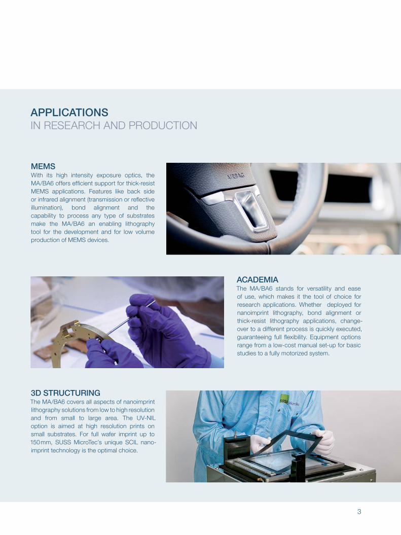
MEMSWith its high intensity exposure optics, the
MA/BA6 offers effi cient support for thick-resist
MEMS applications. Features like back side
or infrared alignment (transmission or refl ective
illumination), bond alignment and the
capability to process any type of substrates
make the MA/BA6 an enabling lithography
tool for the development and for low volume
production of MEMS devices.
ACADEMIAThe MA/BA6 stands for versatility and ease
of use, which makes it the tool of choice for
research applications. Whether deployed for
nanoimprint lithography, bond alignment or
thick-resist lithography applications, change-
over to a different process is quickly executed,
guaranteeing full fl exibility. Equipment options
range from a low-cost manual set-up for basic
studies to a fully motorized system.
3D STRUCTURINGThe MA/BA6 covers all aspects of nanoimprint
lithography solutions from low to high resolution
and from small to large area. The UV-NIL
option is aimed at high resolution prints on
small substrates. For full wafer imprint up to
150 mm, SUSS MicroTec’s unique SCIL nano-
imprint technology is the optimal choice.
APPLICATIONS
IN RESEARCH AND PRODUCTION
4
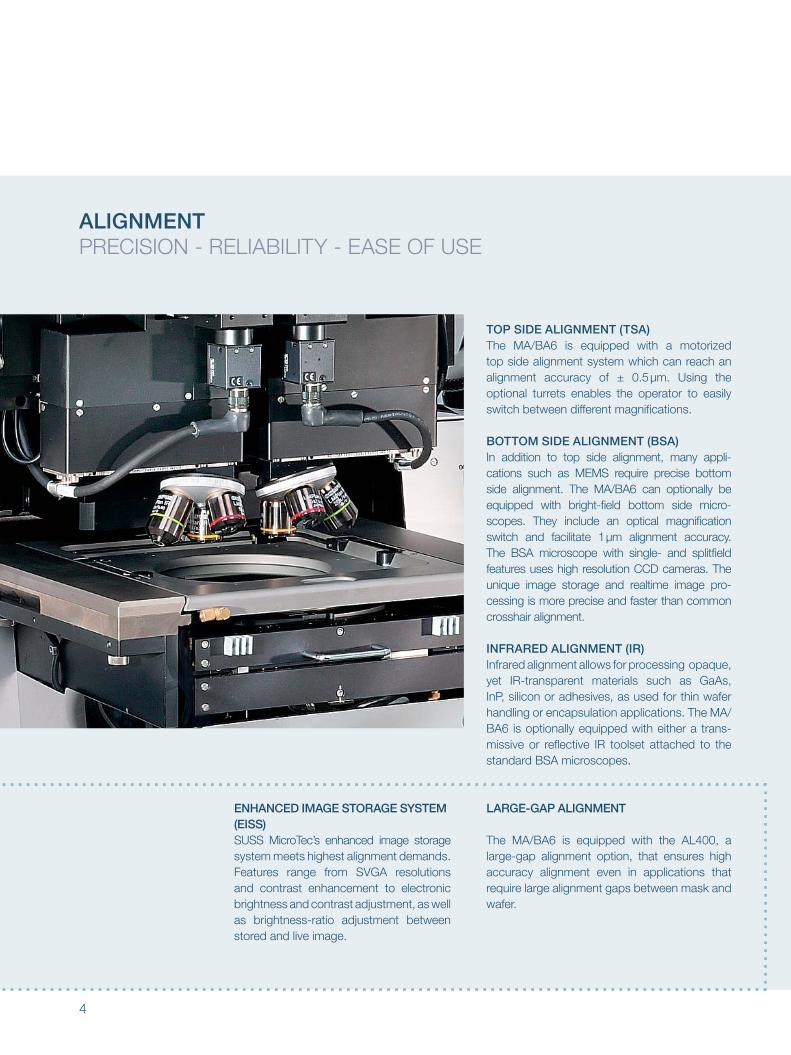
TOP SIDE ALIGNMENT (TSA)
The MA/BA6 is equipped with a motorized
top side alignment system which can reach an
alignment accuracy of ± 0.5 μm. Using the
optional turrets enables the operator to easily
switch between different magnifi cations.
BOTTOM SIDE ALIGNMENT (BSA)
In addition to top side alignment, many appli-
cations such as MEMS require precise bottom
side alignment. The MA/BA6 can optionally be
equipped with bright-fi eld bottom side micro-
scopes. They include an optical magnifi cation
switch and facilitate 1 μm alignment accuracy.
The BSA microscope with single- and splitfi eld
features uses high resolution CCD cameras. The
unique image storage and realtime image pro-
cessing is more precise and faster than common
crosshair alignment.
INFRARED ALIGNMENT (IR)
Infrared alignment allows for processing opaque,
yet IR-transparent materials such as GaAs,
InP, silicon or adhesives, as used for thin wafer
handling or encapsulation applications. The MA/
BA6 is optionally equipped with either a trans-
missive or refl ective IR toolset attached to the
standard BSA microscopes.
ALIGNMENT
PRECISION - RELIABILITY - EASE OF USE
ENHANCED IMAGE STORAGE SYSTEM
(EISS)
SUSS MicroTec’s enhanced image storage
system meets highest alignment demands.
Features range from SVGA resolutions
and contrast enhancement to electronic
brightness and contrast adjustment, as well
as brightness-ratio adjustment between
stored and live image.
LARGE-GAP ALIGNMENT
The MA/BA6 is equipped with the AL400, a
large-gap alignment option, that ensures high
accuracy alignment even in applications that
require large alignment gaps between mask and
wafer.

5
Available Optics Systems in the MA/BA6
- High-Resolution Optics (HR Optics)
- Large-Gap Optics (LGO)
- MO Exposure Optics® (MOEO)
HIGH-RESOLUTION OPTICS
The special HR Optics have been optimized for
highest optical performance in small exposur gaps
or in contact exposure mode.
The high resolution optics achieve resoluti-
on down to 2.5 μm at 20 μm exposure gap and
submicron resolution in contact.
LARGE-GAP OPTICS
SUSS MicroTecs Large-Gap Optics are tailored
to achieve high resolution when exposing in
large mask-to-wafer distances through a dedi-
cated illumination angle setting. This optics are
typically used for applications with high topo-
graphy substrates or thick resist applications.
MO EXPOSURE OPTICS®
MO Exposure Optics are based on unique
high-quality microlens arrays that are combined
with an exchangeable Illumination Filter Plate
(IFP). They provide outstanding light uniformity
and allow quick and easy changeover between
both classical SUSS exposure optics, HR-
and Large-Gap Optics. MO Exposure Optics
additionally allow customized illumination
through modifi cation of the IFP and enable
use of enhanced lithography techniques such
as source-mask optimization (SMO) or Optical
Proximity Correction (OPC).
EXPOSURE OPTICS
TAILORED SOLUTIONS FOR ANY REQUIREMENT
DIFFRACTION REDUCING SYSTEM
SUSS MicroTec’s unique exposure system
minimizes resolution-limiting diffraction effects at
feature edges. The system allows simultaneous
exposure with a certain number of illumination
angles to smooth out the printed features -
a technology that results in signifi cant improve-
ment of resolution and yield.
Strong diffraction effects from parallel illumination (graphics left) vs. SUSS diffraction-reducing op-tics (graphics right). SUSS MicroTec is the only semiconductor equipment supplier offering diffraction reducing optical setups.

6
MA/BA6 RESOLUTION
EXPOSURE MODE UV400 UV300 UV250
Vacuum Contact < 0.8 μm < 0.7 μm < 0.6 μm
Hard Contact < 1.5 μm < 1.0 μm -
Soft Contact < 2.5 μm < 2.0 μm -
Proximity (20 μm) < 3.0 μm < 2.5 μm -
Accurate leveling and gap control of mask and wafer is essential for optimum CD-control. It ensures the parallelism of mask
and substrate during alignment and exposure as well as precise gap control, to avoid parallax errors and to achieve higher
resolution. The leveling and gap calibration system of the MA/BA6 is designed to fulfi ll highest demands with regards to
accuracy and reliability.
WAFER LEVELING AND EXPOSURE GAP CONTROL
PRECISION FOR HIGHEST RESOLUTION
Line, Space resolution achieved on 150 mm Si-wafer in 1.2 μm thick resist AZ 4110 (UV400, UV300) and 0.8 μm thick resist (UV6, UV250) respectively.
Achievable resolution depends on wafer size, wafer fl atness, resist type, clean room condition, and therefore, might vary for different processes.
EXPOSURE MODES
The MA/BA6 offers various exposure modes
to meet any requirements for a broad range of
applications. Soft, hard and vacuum contact
printing is used to achieve highest resolution
down to submicron range. Proximity printing is
applied to avoid any mask/wafer contact. The
prevention of mask contamination directly trans-
lates into higher yield.
EXPOSURE
INTENSITY ADAPTED TO APPLICATION NEEDS
Optical System of a SUSS MA/BA6 Mask Aligner

7
BOND ALIGNMENT
The MA/BA6 offers a highly precise alignment
function for wafer-to-wafer bonding. Based on
SUSS MicroTec´s enhanced image storage
system (EISS), the bond alignment system
achieves alignment accuracy of 0.5 μm. The
SUSS bond fi xture maintains the alignment
precision of the wafer stack during manual
transfer from the aligner to a SUSS bonder
and ensures a controlled gap between the
substrates. The bond alignment functionality
is either integrated in the MA/BA6 or
available as a stand-alone bond aligner,
SUSS BA6/8.
FUSION BONDING
The MA/BA6 supports fusion bonding pro-
cesses in the tool itself. After precise alignment,
the two wafers are brought into direct contact,
thus initiating the fusion pre-bond process in the
bond aligner.
OPTIONSOPTIONAL ENHANCEMENTS
BEYOND STANDARD LITHOGRAPHY
Software simulation of critical features and shortenings, optimized with customized illumi-nation and OPC
Courtesy: FhG IISB
LAB® SIMULATION SOFTWARE
The SUSS version of the LAB lithography simu-
lation software incorporates all SUSS MicroTec
optics solutions, such as HR-, LGO and MO
Exposure Optics including their individual char-
acteristics. The software reduces the need for
experimental layout optimization and simplifi es
process development. Together with MO Ex-
posure Optics, LAB simulation software is the
enabling technology for mask aligner source-
mask optimization.
8
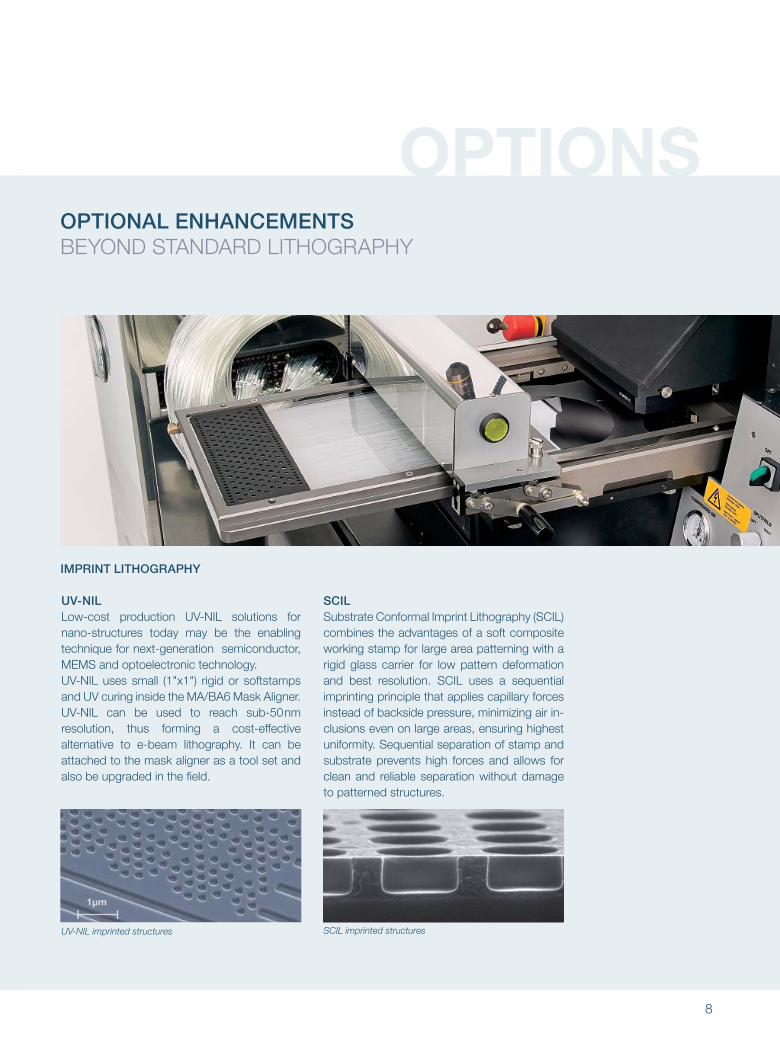
UV-NIL
Low-cost production UV-NIL solutions for
nano-structures today may be the enabling
technique for next-generation semiconductor,
MEMS and optoelectronic technology.
UV-NIL uses small (1"x1") rigid or softstamps
and UV curing inside the MA/BA6 Mask Aligner.
UV-NIL can be used to reach sub-50 nm
resolution, thus forming a cost-effective
alternative to e-beam lithography. It can be
attached to the mask aligner as a tool set and
also be upgraded in the fi eld.
UV-NIL imprinted structures SCIL imprinted structures
SCIL
Substrate Conformal Imprint Lithography (SCIL)
combines the advantages of a soft composite
working stamp for large area patterning with a
rigid glass carrier for low pattern deformation
and best resolution. SCIL uses a sequential
imprinting principle that applies capillary forces
instead of backside pressure, minimizing air in-
clusions even on large areas, ensuring highest
uniformity. Sequential separation of stamp and
substrate prevents high forces and allows for
clean and reliable separation without damage
to patterned structures.
OPTIONSOPTIONAL ENHANCEMENTS
BEYOND STANDARD LITHOGRAPHY
IMPRINT LITHOGRAPHY

9
TECHNICAL DATA
MASK AND WAFER / SUBSTRATE
Wafer Size up to 150 mm
Substrate Size up to 6" x 6"
Pieces down to 5 x 5 mm
Mask Size SEMI spec, standard up to 7" x 7"
EXPOSURE MODES
Contact soft, hard, low vacuum, vacuum
Proximity exposure gap 1-999 μm
Flood Exposure Mode Yes
Gap Setting Accuracy 1 μm
Vacuum Contact adjustable to 200 mbar abs
EXPOSURE OPTICS
Resolution see page 5
down to 0.5 μm
Wavelength Range UV400 350 - 450 nm
UV300 280 - 350 nm
UV250 240 - 260 nm
Exposure Source Hg lamps 200 - 1000 W
HgXe lamp 500 W
Intensity Uniformity ± 5 %
± 2.5 % (MO Exposure Optics)
ALIGNMENT METHODS
Top Side Alignment (TSA); Bottom Side Alignment (BSA); Infrared Alignment
(IR), Large Gap Alignment (AL300)
Dual Focus Alignment System AL400
Enhanced Image Storage Alignment System
Accuracy TSA down to 0.5 μm
Accuracy BSA down to 1 μm
Alignment Gap 1 - 999 μm
1 - 300 μm (with AL300)
ALIGNMENT STAGE
Movement Range X: ± 10 mm
Y: ± 5 mm
θ: ± 5°
Mechanical Accuracy 0.1 μm (step size)
Data, design and specifi cation of custom built machines depend on individual process conditions and can vary according to equipment confi gurations. Not all specifi cations may be valid simultaneously. Illustrations in this brochure are not legally binding. SUSS MicroTec reserves the right to change machine specifi cations without prior notice.
TSA MICROSCOPE STAGE
Single Field X: ± 25 mm
Y: ± 25/-75 mm
Split Field X: ± 25 mm
Y: ± 15/-75 mm; θ: ± 3°
X: optional ± 50 mm
TOPSIDE MICROSCOPE TSA
Single Field M500 up to 200 x
Split Field M306 up to 335 x
DVM6 up to 1045 x (17" screen)
IRDVM6 up to 1045 x (17" screen)
Objective Magnifi cation standard 2.5x, 5 x, 10 x, 20 x
optional 5 x IR, 10 x IR
Split Field Objective Separation with turret: 32-160 mm
without turret: 27-160 mm
BOTTOMSIDE SPLITFIELD MICROSCOPE BSA
Objective Separation 15 - 100 mm
(62 - 148 mm optional)
Movement Range Y: + 50/- 20 mm
Magnifi cation 112/355 on 17" screen
Field of View 0.92 x 0.69 mm2
(high magnifi cation, full fi eld)
UTILITIES
Vacuum <-0.8 bar, 200 mbar abs
Compressed Air 5 bar (75 psi)
Nitrogen > 1 bar (15 psi)
With 350 W Lamp
With 1000 W Lamp
0.3 m3/h
0.9 m3/h
POWER REQUIREMENTS
Power Voltage AC 230 V
Frequency 50 - 60 Hz
Consumption with
350 W Lamp
500 W Lamp
1000 W Lamp
1500 W
1700 W
2300 W
PHYSICAL DIMENSIONS
H x W x D (LH1000) 1570 x 1214 x 1300 mm
H x W x D (LH350) 1535 x 1214 x 1300 mm
Weight 320 - 340 kg

www.suss.com
Visit www.suss.com/locations for your nearest SUSS representative or contact us:
SÜSS MicroTec AG | Phone: +49 89 32 007-0 | [email protected]
NORTH AMERICA EUROPE ASIA
USA Singapore China
Korea
Japan
Taiwan
Germany
Switzerland
France
United Kingdom
Headquarters
Production
SalesM
A/B
A6
· 0
9/20
14 ·
BR
_M
AB
A6_
2014
· V
2