BLF988; BLF988S - ampleon.com · A 600WLDMOS RF power transistor for transmitter applications and...
18
1. Product profile 1.1 General description A 600 W LDMOS RF power transistor for transmitter applications and industrial applications. The excellent ruggedness of this device makes it ideal for digital and analog transmitter applications. 1.2 Features and benefits Excellent ruggedness (VSWR 40 : 1 through all phases) Optimum thermal behavior and reliability, R th(j-c) = 0.15 K/W High power gain High efficiency Designed for broadband operation (400 MHz to 1000 MHz) Internal input matching for high gain and optimum broadband operation Excellent reliability Easy power control Compliant to Directive 2002/95/EC, regarding Restriction of Hazardous Substances (RoHS) 1.3 Applications Communication transmitter applications Industrial applications BLF988; BLF988S Power LDMOS transistor Rev. 3 — 1 September 2015 Product data sheet Table 1. Application information Test signal f P L(AV) P L(M) G p D IMD3 (MHz) (W) (W) (dB) (%) (dBc) RF performance in a common source 860 MHz narrowband test circuit 2-tone, class-AB f 1 = 860; f 2 = 860.1 250 - 20.8 46 32 pulsed, class-AB 860 - 600 19.8 58 -
-
Upload
hoangxuyen -
Category
Documents
-
view
215 -
download
0
Transcript of BLF988; BLF988S - ampleon.com · A 600WLDMOS RF power transistor for transmitter applications and...

1. Product profile
1.1 General description
A 600 W LDMOS RF power transistor for transmitter applications and industrial applications. The excellent ruggedness of this device makes it ideal for digital and analog transmitter applications.
1.2 Features and benefits
Excellent ruggedness (VSWR 40 : 1 through all phases)
Optimum thermal behavior and reliability, Rth(j-c) = 0.15 K/W
High power gain
High efficiency
Designed for broadband operation (400 MHz to 1000 MHz)
Internal input matching for high gain and optimum broadband operation
Excellent reliability
Easy power control
Compliant to Directive 2002/95/EC, regarding Restriction of Hazardous Substances (RoHS)
1.3 Applications
Communication transmitter applications
Industrial applications
BLF988; BLF988SPower LDMOS transistorRev. 3 — 1 September 2015 Product data sheet
Table 1. Application information
Test signal f PL(AV) PL(M) Gp D IMD3
(MHz) (W) (W) (dB) (%) (dBc)
RF performance in a common source 860 MHz narrowband test circuit
2-tone, class-AB f1 = 860; f2 = 860.1 250 - 20.8 46 32
pulsed, class-AB 860 - 600 19.8 58 -

BLF988; BLF988SPower LDMOS transistor
2. Pinning information
[1] Connected to flange.
3. Ordering information
4. Limiting values
[1] Continuous use at maximum temperature will affect the reliability. For details refer to the on-line MTF calculator.
Table 2. Pinning
Pin Description Simplified outline Graphic symbol
BLF988 (SOT539A)
1 drain1
2 drain2
3 gate1
4 gate2
5 source [1]
BLF988S (SOT539B)
1 drain1
2 drain2
3 gate1
4 gate2
5 source [1]
5
1 2
434
35
1
2sym117
5
1 2
434
35
1
2sym117
Table 3. Ordering information
Type number Package
Name Description Version
BLF988 - flanged balanced ceramic package; 2 mounting holes; 4 leads SOT539A
BLF988S - earless flanged balanced ceramic package; 4 leads SOT539B
Table 4. Limiting valuesIn accordance with the Absolute Maximum Rating System (IEC 60134).
Symbol Parameter Conditions Min Max Unit
VDS drain-source voltage - 110 V
VGS gate-source voltage 0.5 +11 V
Tstg storage temperature 65 +150 C
Tj junction temperature [1] - 225 C
BLF988_BLF988S#3 All information provided in this document is subject to legal disclaimers. © Ampleon The Netherlands B.V. 2015. All rights reserved.
Product data sheet Rev. 3 — 1 September 2015 2 of 18

BLF988; BLF988SPower LDMOS transistor
5. Thermal characteristics
[1] Rth(j-c) is measured under RF conditions.
6. Characteristics
[1] ID is the drain current.
[1] Capacitance values without internal matching.
Table 5. Thermal characteristics
Symbol Parameter Conditions Typ Unit
Rth(j-c) thermal resistance from junction to case Tcase = 80 C; PL(AV) = 250 W [1] 0.15 K/W
Table 6. DC characteristicsTj = 25 C; per section unless otherwise specified.
Symbol Parameter Conditions Min Typ Max Unit
V(BR)DSS drain-source breakdown voltage VGS = 0 V; ID = 2.4 mA [1] 110 - - V
VGS(th) gate-source threshold voltage VDS = 10 V; ID = 240 mA [1] 1.4 1.9 2.4 V
IDSS drain leakage current VGS = 0 V; VDS = 50 V - - 2.8 A
IDSX drain cut-off current VGS = VGS(th) + 3.75 V; VDS = 10 V
- 36 - A
IGSS gate leakage current VGS = 10 V; VDS = 0 V - - 280 nA
RDS(on) drain-source on-state resistance VGS = VGS(th) + 3.75 V; ID = 8.5 A
[1] - 143 - m
Table 7. AC characteristicsTj = 25 C; per section unless otherwise specified.
Symbol Parameter Conditions Min Typ Max Unit
Ciss input capacitance VGS = 0 V; VDS = 50 V; f = 1 MHz [1] - 220 - pF
Coss output capacitance VGS = 0 V; VDS = 50 V; f = 1 MHz - 74 - pF
Crss reverse transfer capacitance
VGS = 0 V; VDS = 50 V; f = 1 MHz - 1.2 - pF
Table 8. RF characteristicsRF characteristics in Ampleon production narrowband test circuit; Tcase = 25 C unless otherwise specified.
Symbol Parameter Conditions Min Typ Max Unit
2-Tone, class-AB
VDS drain-source voltage - 50 - V
IDq quiescent drain current [1] - 1.3 - A
PL(AV) average output power f1 = 860 MHz; f2 = 860.1 MHz 250 - - W
Gp power gain f1 = 860 MHz; f2 = 860.1 MHz 19.8 20.8 - dB
D drain efficiency f1 = 860 MHz; f2 = 860.1 MHz 42 46 - %
IMD3 third-order intermodulation distortion
f1 = 860 MHz; f2 = 860.1 MHz - 32 28 dBc
BLF988_BLF988S#3 All information provided in this document is subject to legal disclaimers. © Ampleon The Netherlands B.V. 2015. All rights reserved.
Product data sheet Rev. 3 — 1 September 2015 3 of 18
BLF988; BLF988SPower LDMOS transistor
[1] IDq for total device
7. Test information
7.1 Ruggedness in class-AB operation
The BLF988 and BLF988S are capable of withstanding a load mismatch corresponding to VSWR 40 : 1 through all phases under the following conditions: VDS = 50 V; IDq = 1.3 A; PL = 600 W (pulsed); f = 860 MHz.
Pulsed, class-AB
VDS drain-source voltage - 50 - V
IDq quiescent drain current [1] - 1.3 - A
PL(M) peak output power f = 860 MHz - 600 - W
Gp power gain f = 860 MHz 17.2 19.8 - dB
D drain efficiency f = 860 MHz 54 58 - %
tp pulse duration - 100 - s
duty cycle - 20 - %
VGS = 0 V; f = 1 MHz.
Fig 1. Output capacitance as a function of drain-source voltage; typical values per section
Table 8. RF characteristics …continuedRF characteristics in Ampleon production narrowband test circuit; Tcase = 25 C unless otherwise specified.
Symbol Parameter Conditions Min Typ Max Unit
001aam579
VDS (V)0 604020
200
100
300
400
Coss(pF)
0
BLF988_BLF988S#3 All information provided in this document is subject to legal disclaimers. © Ampleon The Netherlands B.V. 2015. All rights reserved.
Product data sheet Rev. 3 — 1 September 2015 4 of 18
BLF988; BLF988SPower LDMOS transistor
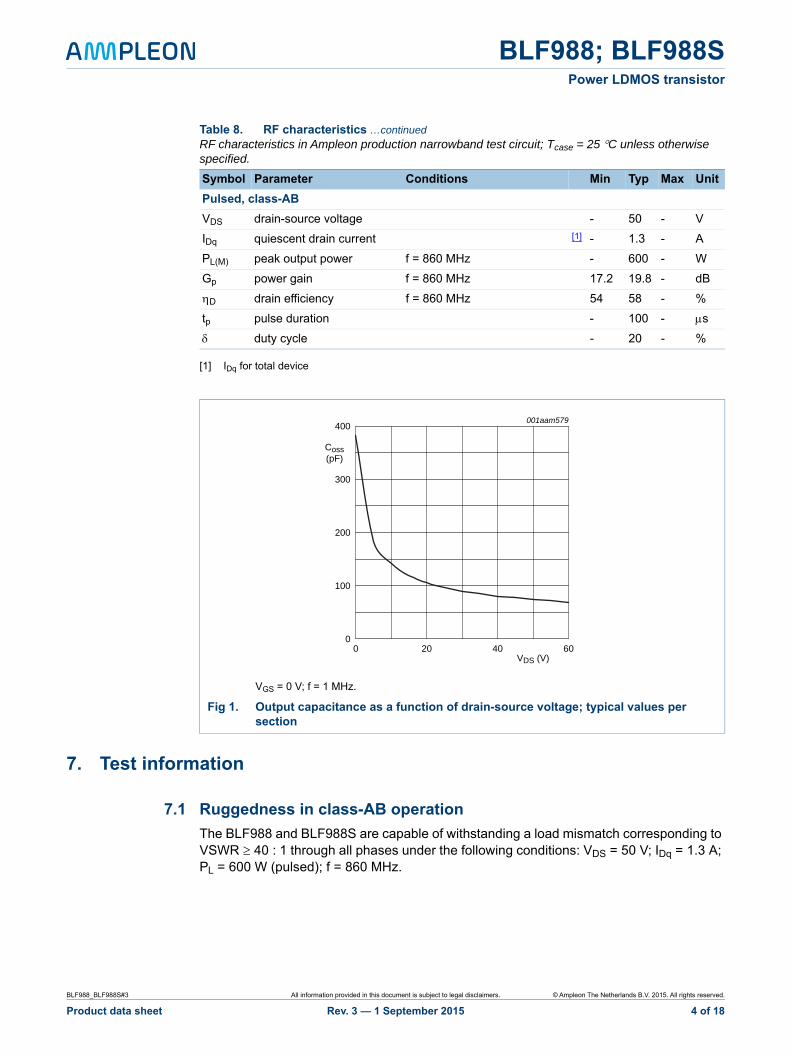
7.2 Impedance information
Table 9. Typical push-pull impedanceSimulated Zi and ZL device impedance; impedance info at VDS = 50 V and PL(AV) = 600 W (pulsed CW). See Figure 2 for definition of transistor impedance.
f Zi ZL
MHz
300 0.607 + j0 5.495 + j1.936
325 0.622 j1.441 5.324 + j2.008
350 0.639 j1.121 5.151 + j2.065
375 0.658 j0.826 4.977 + j2.107
400 0.679 j0.551 4.805 + j2.136
425 0.703 j0.291 4.634 + j2.153
450 0.73 j0.044 4.466 + j2.157
475 0.76 + j0.194 4.301 + j2.151
500 0.793 + j0.424 4.14 + j2.134
525 0.83 + j0.648 3.984 + j2.109
550 0.872 + j0.869 3.833 + j2.075
575 0.919 + j1.088 3.687 + j2.033
600 0.972 + j1.305 3.546 + j1.985
625 1.032 + j1.523 3.411 + j1.931
650 1.101 + j1.741 3.281 + j1.871
675 1.179 + j1.963 3.156 + j1.807
700 1.268 + j2.187 3.036 + j1.738
725 1.371 + j2.416 2.922 + j1.666
750 1.49 + j2.651 2.813 + j1.591
775 1.629 + j2.891 2.708 + j1.512
800 1.792 + j3.138 2.609 + j1.432
825 1.984 + j3.39 2.514 + j1.349
850 2.212 + j3.649 2.423 + j1.264
875 2.484 + j3.91 2.336 + j1.178
900 2.812 + j4.17 2.254 + j1.091
925 3.209 + j4.421 2.175 + j1.003
950 3.689 + j4.648 2.1 + j0.913
975 4.27 + j4.829 2.029 + j0.823
1000 4.967 + j4.927 1.96 + j0.733
BLF988_BLF988S#3 All information provided in this document is subject to legal disclaimers. © Ampleon The Netherlands B.V. 2015. All rights reserved.
Product data sheet Rev. 3 — 1 September 2015 5 of 18
BLF988; BLF988SPower LDMOS transistor
7.3 Test circuit information
Fig 2. Definition of transistor impedance
001aan207
gate 1
gate 2
drain 2
drain 1
Zi ZL
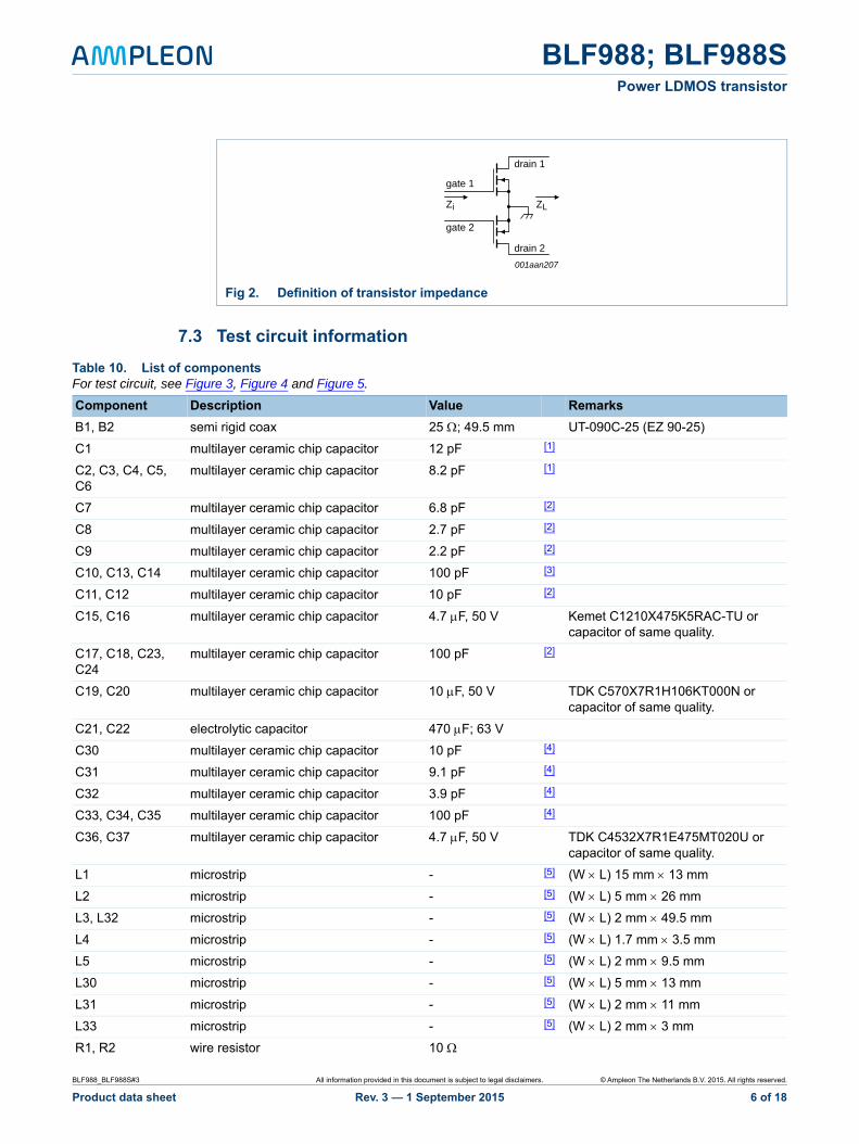
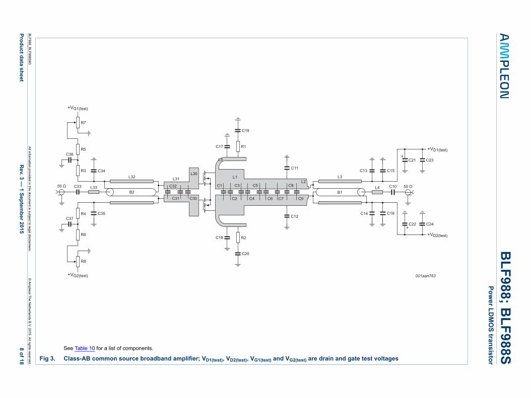
Table 10. List of componentsFor test circuit, see Figure 3, Figure 4 and Figure 5.
Component Description Value Remarks
B1, B2 semi rigid coax 25 ; 49.5 mm UT-090C-25 (EZ 90-25)
C1 multilayer ceramic chip capacitor 12 pF [1]
C2, C3, C4, C5, C6
multilayer ceramic chip capacitor 8.2 pF [1]
C7 multilayer ceramic chip capacitor 6.8 pF [2]
C8 multilayer ceramic chip capacitor 2.7 pF [2]
C9 multilayer ceramic chip capacitor 2.2 pF [2]
C10, C13, C14 multilayer ceramic chip capacitor 100 pF [3]
C11, C12 multilayer ceramic chip capacitor 10 pF [2]
C15, C16 multilayer ceramic chip capacitor 4.7 F, 50 V Kemet C1210X475K5RAC-TU or capacitor of same quality.
C17, C18, C23, C24
multilayer ceramic chip capacitor 100 pF [2]
C19, C20 multilayer ceramic chip capacitor 10 F, 50 V TDK C570X7R1H106KT000N or capacitor of same quality.
C21, C22 electrolytic capacitor 470 F; 63 V
C30 multilayer ceramic chip capacitor 10 pF [4]
C31 multilayer ceramic chip capacitor 9.1 pF [4]
C32 multilayer ceramic chip capacitor 3.9 pF [4]
C33, C34, C35 multilayer ceramic chip capacitor 100 pF [4]
C36, C37 multilayer ceramic chip capacitor 4.7 F, 50 V TDK C4532X7R1E475MT020U or capacitor of same quality.
L1 microstrip - [5] (W L) 15 mm 13 mm
L2 microstrip - [5] (W L) 5 mm 26 mm
L3, L32 microstrip - [5] (W L) 2 mm 49.5 mm
L4 microstrip - [5] (W L) 1.7 mm 3.5 mm
L5 microstrip - [5] (W L) 2 mm 9.5 mm
L30 microstrip - [5] (W L) 5 mm 13 mm
L31 microstrip - [5] (W L) 2 mm 11 mm
L33 microstrip - [5] (W L) 2 mm 3 mm
R1, R2 wire resistor 10
BLF988_BLF988S#3 All information provided in this document is subject to legal disclaimers. © Ampleon The Netherlands B.V. 2015. All rights reserved.
Product data sheet Rev. 3 — 1 September 2015 6 of 18

BLF988; BLF988SPower LDMOS transistor
[1] American technical ceramics type 800R or capacitor of same quality.
[2] American technical ceramics type 800B or capacitor of same quality.
[3] American technical ceramics type 180R or capacitor of same quality.
[4] American technical ceramics type 100A or capacitor of same quality.
[5] Printed-Circuit Board (PCB): Taconic RF35; r = 3.5 F/m; height = 0.762 mm; Cu (top/bottom metallization); thickness copper plating = 35 m.
R3, R4 SMD resistor 5.6 0805
R5, R6 wire resistor 100
R7, R8 potentiometer 10 k
Table 10. List of components …continuedFor test circuit, see Figure 3, Figure 4 and Figure 5.
Component Description Value Remarks
BLF988_BLF988S#3 All information provided in this document is subject to legal disclaimers. © Ampleon The Netherlands B.V. 2015. All rights reserved.
Product data sheet Rev. 3 — 1 September 2015 7 of 18
xxxxxxxxxxxxxxxxxxxxx xxxxxxxxxxxxxxxxxxxxxxxxxx xxxxxxx x x x xxxxxxxxxxxxxxxxxxxxxxxxxxxxxx xxxxxxxxxxxxxxxxxxx xx xx xxxxx xxxxxxxxxxxxxxxxxxxxxxxxxxx xxxxxxxxxxxxxxxxxxx xxxxxx xxxxxxxxxxxxxxxxxxxxxxxxxxxxxxxxxxx xxxxxxxxxxxx x x xxxxxxxxxxxxxxxxxxxxx xxxxxxxxxxxxxxxxxxxxxxxxxxxxxx xxxxx xxxxxxxxxxxxxxxxxxxxxxxxxxxxxxxxxxxxxxxxxxxxxxxxxx xxxxxxxx xxxxxxxxxxxxxxxxxxxxxxxxx xxxxxxxxxxxxxxxxxxxx xxx
BLF
988_B
LF
988
Pro
du
ct data sh
eet
Rev. 3
— 1 S
eptem
ber 2015
8 o
f 18
BL
F988; B
LF
988SP
ow
er L
DM
OS
tran
sis
tor voltages
+VD1(test)
+VD2(test)
C15
C10 50 ΩL4
C21
C22
C16
001aan763
C23
C24
S#3
All inform
ation provided in this docum
ent is su
bject to legal disclaimers.
© A
mpleon T
he Ne
therlands B
.V. 2
015. All rights reserved
.
See Table 10 for a list of components.
Fig 3. Class-AB common source broadband amplifier; VD1(test), VD2(test), VG1(test) and VG2(test) are drain and gate test
+VG1(test)
C32
C31 C30
C19
C20
50 Ω
C13
C14
C9C7C6C4
C8C5C3
C2
C1
+VG2(test)
L30L1
L2
R1
L5
L31
C34
C36
C33
C37
L33
C35
L3
B1
R3L32
B2
R4
R6
R8
R5
R7
C11
C12
C17
R2C18

BLF988; BLF988SPower LDMOS transistor
See Table 10 for a list of components.
Fig 4. Printed-Circuit Board (PCB) for class-AB common source amplifier
50 mm
001aam588105 mm
L33
L32
L32
L31
L30
L30
L1
L5
L5
L1
L2
L2
L3
L3
L4L31
See Table 10 for a list of components.
Fig 5. Component layout for class-AB common source amplifier
-
+
-
+
6.3 mm
4 mm
+VG2(test) +VD2(test)
+VD1(test)+VG1(test)
001aan764
R8
R7
R6C37
C35
C34C32 C30
C31
C36
C17
C19
C11
C12
C7 C9
C8
C1
C2
C3
C4
C5
C6
C21
C23
C24
C22
C20
C18R2
C15
C13
C14
C16
R1
C3350 Ω
C10
50 Ω
R4
R3
R5
49.6 mm
36.8 mm26.3 mm25.3 mm
44 mm
BLF988_BLF988S#3 All information provided in this document is subject to legal disclaimers. © Ampleon The Netherlands B.V. 2015. All rights reserved.
Product data sheet Rev. 3 — 1 September 2015 9 of 18

BLF988; BLF988SPower LDMOS transistor
7.4 Graphical data
7.4.1 Pulsed
VDS = 50 V; IDq = 1300 mA; f = 860 MHz; tp = 100 s; = 20 %.
(1) PL(1dB) = 57.6 dBm (575 W)
(2) PL(3dB) = 58.1 dBm (649 W)
VDS = 50 V; f = 860 MHz; tp = 100 s; = 20 %.
(1) IDq = 100 mA
(2) IDq = 200 mA
(3) IDq = 600 mA
(4) IDq = 1000 mA
(5) IDq = 1300 mA
Fig 6. Output power as a function of input power; typical values
Fig 7. Power gain as a function of output power; typical values
Pi (dBm)413935 40383634 37
aaa-007877
59
57
61
63
PL(dBm)
55
Ideal PL
PL
(1)
(2)
aaa-007878
0 100 200 300 400 500 600 70015
17
19
21
23
PL (W)
GpGp(dB)(dB)(dB)
(1)(1)(1)(2)(2)(2)
(3)(3)(3)
(4)(4)(4)(5)(5)(5)
BLF988_BLF988S#3 All information provided in this document is subject to legal disclaimers. © Ampleon The Netherlands B.V. 2015. All rights reserved.
Product data sheet Rev. 3 — 1 September 2015 10 of 18

BLF988; BLF988SPower LDMOS transistor
VDS = 50 V; f = 860 MHz; tp = 100 s; = 20 %.
(1) IDq = 100 mA
(2) IDq = 200 mA
(3) IDq = 600 mA
(4) IDq = 1000 mA
(5) IDq = 1300 mA
VDS = 50 V; IDq = 1300 mA; f = 860 MHz; tp = 100 s; = 20 %.
Fig 8. Drain efficiency as a function of output power; typical values
Fig 9. Power gain and drain efficiency as function of output power; typical values
IDq = 1300 mA; f = 860 MHz; tp = 100 s; = 20 %.
(1) VDS = 50 V
(2) VDS = 45 V
(3) VDS = 40 V
(4) VDS = 35 V
(5) VDS = 30 V
IDq = 1300 mA; f = 860 MHz; tp = 100 s; = 20 %.
(1) VDS = 50 V
(2) VDS = 45 V
(3) VDS = 40 V
(4) VDS = 35 V
(5) VDS = 30 V
Fig 10. Power gain as a function of output power; typical values
Fig 11. Drain efficiency as a function of output power; typical values
aaa-007879
0 100 200 300 400 500 600 7000
20
40
60
80
PL (W)
ηDηD(%)(%)(%)
(1)(1)(1)(2)(2)(2)(3)(3)(3)(4)(4)(4)(5)(5)(5)
aaa-007880
0 100 200 300 400 500 600 70018 0
19 20
20 40
21 60
22 80
PL (W)
GpGp(dB)(dB)(dB)
ηDηD(%)(%)(%)
GpGp
ηDηD
aaa-007881
0 100 200 300 400 500 600 70016
18
20
22
24
PL (W)
GpGp(dB)(dB)(dB)
(1)(1)(1)(2)(2)(2)(3)(3)(3)
(4)(4)(4)(5)(5)(5)
aaa-007882
0 100 200 300 400 500 600 7000
20
40
60
80
PL (W)
ηDηD(%)(%)(%)
(1)(1)(1)(2)(2)(2)(3)(3)(3)(4)(4)(4)
(5)(5)(5)
BLF988_BLF988S#3 All information provided in this document is subject to legal disclaimers. © Ampleon The Netherlands B.V. 2015. All rights reserved.
Product data sheet Rev. 3 — 1 September 2015 11 of 18
BLF988; BLF988SPower LDMOS transistor
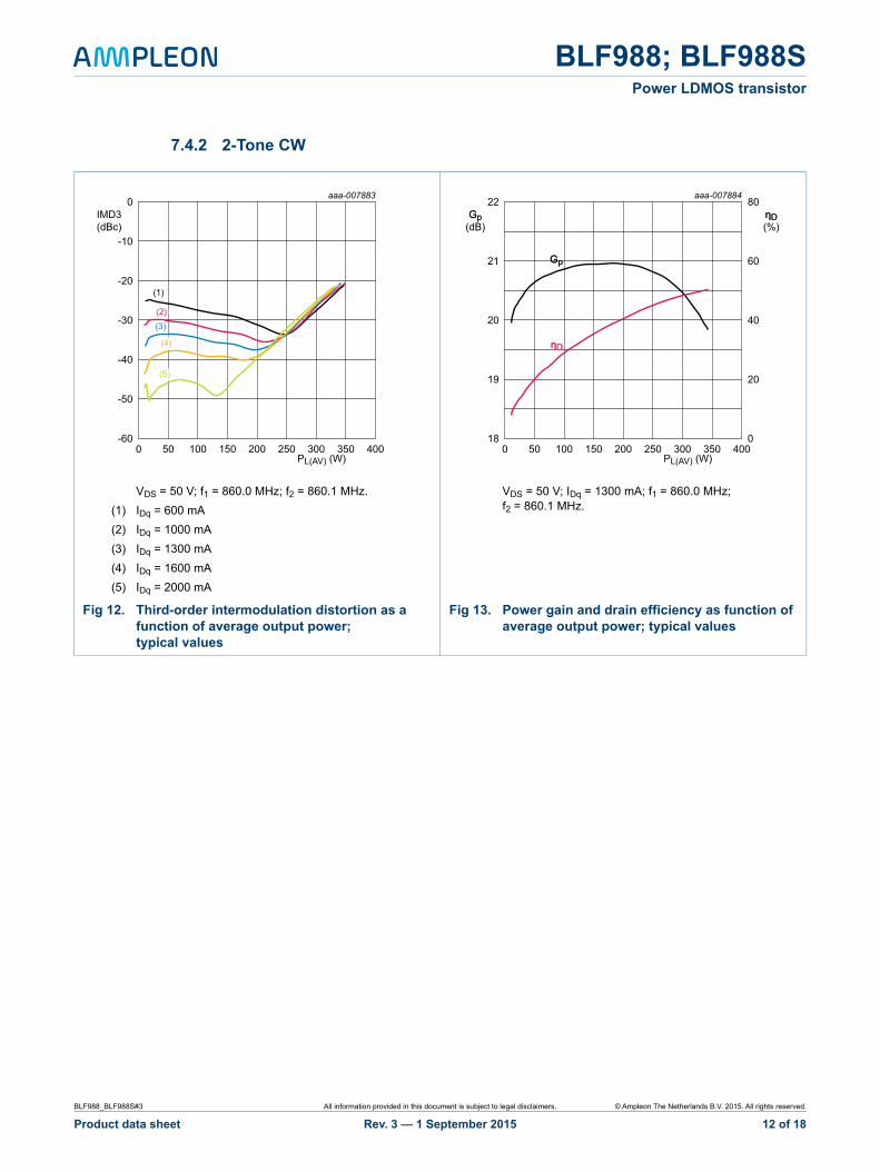
7.4.2 2-Tone CW
VDS = 50 V; f1 = 860.0 MHz; f2 = 860.1 MHz.
(1) IDq = 600 mA
(2) IDq = 1000 mA
(3) IDq = 1300 mA
(4) IDq = 1600 mA
(5) IDq = 2000 mA
VDS = 50 V; IDq = 1300 mA; f1 = 860.0 MHz; f2 = 860.1 MHz.
Fig 12. Third-order intermodulation distortion as a function of average output power; typical values
Fig 13. Power gain and drain efficiency as function of average output power; typical values
aaa-007883
0 50 100 150 200 250 300 350 400-60
-50
-40
-30
-20
-10
0
PL(AV) (W)
IMD3IMD3IMD3(dBc)(dBc)(dBc)
(1)(1)(1)
(2)(2)(2)(3)(3)(3)
(4)(4)(4)
(5)(5)(5)
aaa-007884
0 50 100 150 200 250 300 350 40018 0
19 20
20 40
21 60
22 80
PL(AV) (W)
GpGp(dB)(dB)(dB)
ηDηD(%)(%)(%)
GpGp
ηDηD
BLF988_BLF988S#3 All information provided in this document is subject to legal disclaimers. © Ampleon The Netherlands B.V. 2015. All rights reserved.
Product data sheet Rev. 3 — 1 September 2015 12 of 18

BLF988; BLF988SPower LDMOS transistor
8. Package outline
Fig 14. Package outline SOT539A
REFERENCESOUTLINEVERSION
EUROPEANPROJECTION ISSUE DATE
IEC JEDEC EIAJ
SOT539A 12-05-0210-02-02
0 5 10 mm
scale
p
AF
b
e
D
U2
L
H
Q
c
5
1 2
43
D1
E
A
w1 A BM M M
q
U1
H1
C
B
M Mw2 C
E1
Mw3
UNIT A
mm
Db
11.8111.56
0.180.10
31.5530.94 13.72 9.53
9.2717.1216.10
10.2910.03
4.74.2
c e U2
0.250.25 0.51
w3
35.56
q w2w1F
1.751.50
U1
41.2841.02
H1
25.5325.27
p
3.303.05
Q
2.262.01
E E1
9.509.30
inches 0.4650.455
0.0070.004
1.2421.218
D1
31.5230.96
1.2411.219 0.540 0.375
0.3650.6740.634
0.4050.395
0.1850.165 0.0100.010 0.0201.4000.069
0.0591.6251.615
1.0050.995
0.1300.120
0.0890.079
0.3740.366
H
3.482.97
0.1370.117
L
DIMENSIONS (millimetre dimensions are derived from the original inch dimensions)
Flanged balanced ceramic package; 2 mounting holes; 4 leads SOT539A
Note1. millimeter dimensions are derived from the original inch dimensions.2. recommended screw pitch dimension of 1.52 inch (38.6 mm) based on M3 screw.
BLF988_BLF988S#3 All information provided in this document is subject to legal disclaimers. © Ampleon The Netherlands B.V. 2015. All rights reserved.
Product data sheet Rev. 3 — 1 September 2015 13 of 18

BLF988; BLF988SPower LDMOS transistor
Fig 15. Package outline SOT539B
ReferencesOutlineversion
Europeanprojection Issue date
IEC JEDEC JEITA
SOT539B
sot539b_po
12-05-0213-05-24
Unit(1)
mmmaxnommin
4.7
4.2
11.81
11.56
31.55
30.94
31.52
30.96
9.5
9.3
9.53
9.27
1.75
1.50
17.12
16.10
3.48
2.97
10.29
10.030.25
A
Dimensions
Earless flanged balanced ceramic package; 4 leads SOT539B
b c
0.18
0.10
D D1 E E1 e
13.72
F H H1
25.53
25.27
L Q
2.26
2.01
U1
32.39
32.13
U2 w2
0.25
inchesmaxnommin
0.185
0.165
0.465
0.455
1.242
1.218
1.241
1.219
0.374
0.366
0.375
0.365
0.069
0.059
0.674
0.634
0.137
0.117
0.405
0.3950.01
0.007
0.0040.54
1.005
0.995
0.089
0.079
1.275
1.2650.01
w3
0 5 10 mm
scale
c
E
Q
E1
e
H
L
b
H1
U1
U2
Dw2
w3
1 2
3 4
D
D
AF
D1
5
Note1. millimeter dimensions are derived from the original inch dimensions.
BLF988_BLF988S#3 All information provided in this document is subject to legal disclaimers. © Ampleon The Netherlands B.V. 2015. All rights reserved.
Product data sheet Rev. 3 — 1 September 2015 14 of 18

BLF988; BLF988SPower LDMOS transistor
9. Handling information
10. Abbreviations
11. Revision history
CAUTION
This device is sensitive to ElectroStatic Discharge (ESD). Observe precautions for handling electrostatic sensitive devices.
Such precautions are described in the ANSI/ESD S20.20, IEC/ST 61340-5, JESD625-A or equivalent standards.
Table 11. Abbreviations
Acronym Description
CCDF Complementary Cumulative Distribution Function
CW Continuous Wave
LDMOS Laterally Diffused Metal-Oxide Semiconductor
SMD Surface Mounted Device
VSWR Voltage Standing-Wave Ratio
Table 12. Revision history
Document ID Release date Data sheet status Change notice Supersedes
BLF988_BLF988S#3 20150901 Product data sheet BLF988_BLF988S v.2
Modifications: • The format of this document has been redesigned to comply with the new identity guidelines of Ampleon.
• Legal texts have been adapted to the new company name where appropriate.
BLF988_BLF988S v.2 20130801 Product data sheet - BLF988_BLF988S v.1
BLF988_BLF988S v.1 20121009 Objective data sheet - -
BLF988_BLF988S#3 All information provided in this document is subject to legal disclaimers. © Ampleon The Netherlands B.V. 2015. All rights reserved.
Product data sheet Rev. 3 — 1 September 2015 15 of 18

BLF988; BLF988SPower LDMOS transistor
12. Legal information
12.1 Data sheet status
[1] Please consult the most recently issued document before initiating or completing a design.
[2] The term ‘short data sheet’ is explained in section “Definitions”.
[3] The product status of device(s) described in this document may have changed since this document was published and may differ in case of multiple devices. The latest product status information is available on the Internet at URL http://www.ampleon.com.
12.2 Definitions
Draft — The document is a draft version only. The content is still under internal review and subject to formal approval, which may result in modifications or additions. Ampleon does not give any representations or warranties as to the accuracy or completeness of information included herein and shall have no liability for the consequences of use of such information.
Short data sheet — A short data sheet is an extract from a full data sheet with the same product type number(s) and title. A short data sheet is intended for quick reference only and should not be relied upon to contain detailed and full information. For detailed and full information see the relevant full data sheet, which is available on request via the local Ampleon sales office. In case of any inconsistency or conflict with the short data sheet, the full data sheet shall prevail.
Product specification — The information and data provided in a Product data sheet shall define the specification of the product as agreed between Ampleon and its customer, unless Ampleon and customer have explicitly agreed otherwise in writing. In no event however, shall an agreement be valid in which the Ampleon product is deemed to offer functions and qualities beyond those described in the Product data sheet.
12.3 Disclaimers
Limited warranty and liability — Information in this document is believed to be accurate and reliable. However, Ampleon does not give any representations or warranties, expressed or implied, as to the accuracy or completeness of such information and shall have no liability for the consequences of use of such information. Ampleon takes no responsibility for the content in this document if provided by an information source outside of Ampleon.
In no event shall Ampleon be liable for any indirect, incidental, punitive, special or consequential damages (including - without limitation - lost profits, lost savings, business interruption, costs related to the removal or replacement of any products or rework charges) whether or not such damages are based on tort (including negligence), warranty, breach of contract or any other legal theory.
Notwithstanding any damages that customer might incur for any reason whatsoever, Ampleon’ aggregate and cumulative liability towards customer for the products described herein shall be limited in accordance with the Terms and conditions of commercial sale of Ampleon.
Right to make changes — Ampleon reserves the right to make changes to information published in this document, including without limitation specifications and product descriptions, at any time and without notice. This document supersedes and replaces all information supplied prior to the publication hereof.
Suitability for use — Ampleon products are not designed, authorized or warranted to be suitable for use in life support, life-critical or safety-critical systems or equipment, nor in applications where failure or malfunction of an
Ampleon product can reasonably be expected to result in personal injury, death or severe property or environmental damage. Ampleon and its suppliers accept no liability for inclusion and/or use of Ampleon products in such equipment or applications and therefore such inclusion and/or use is at the customer’s own risk.
Applications — Applications that are described herein for any of these products are for illustrative purposes only. Ampleon makes no representation or warranty that such applications will be suitable for the specified use without further testing or modification.
Customers are responsible for the design and operation of their applications and products using Ampleon products, and Ampleon accepts no liability for any assistance with applications or customer product design. It is customer’s sole responsibility to determine whether the Ampleon product is suitable and fit for the customer’s applications and products planned, as well as for the planned application and use of customer’s third party customer(s). Customers should provide appropriate design and operating safeguards to minimize the risks associated with their applications and products.
Ampleon does not accept any liability related to any default, damage, costs or problem which is based on any weakness or default in the customer’s applications or products, or the application or use by customer’s third party customer(s). Customer is responsible for doing all necessary testing for the customer’s applications and products using Ampleon products in order to avoid a default of the applications and the products or of the application or use by customer’s third party customer(s). Ampleon does not accept any liability in this respect.
Limiting values — Stress above one or more limiting values (as defined in the Absolute Maximum Ratings System of IEC 60134) will cause permanent damage to the device. Limiting values are stress ratings only and (proper) operation of the device at these or any other conditions above those given in the Recommended operating conditions section (if present) or the Characteristics sections of this document is not warranted. Constant or repeated exposure to limiting values will permanently and irreversibly affect the quality and reliability of the device.
Terms and conditions of commercial sale — Ampleon products are sold subject to the general terms and conditions of commercial sale, as published at http://www.ampleon.com/terms, unless otherwise agreed in a valid written individual agreement. In case an individual agreement is concluded only the terms and conditions of the respective agreement shall apply. Ampleon hereby expressly objects to applying the customer’s general terms and conditions with regard to the purchase of Ampleon products by customer.
No offer to sell or license — Nothing in this document may be interpreted or construed as an offer to sell products that is open for acceptance or the grant, conveyance or implication of any license under any copyrights, patents or other industrial or intellectual property rights.
Export control — This document as well as the item(s) described herein may be subject to export control regulations. Export might require a prior authorization from competent authorities.
Document status[1][2] Product status[3] Definition
Objective [short] data sheet Development This document contains data from the objective specification for product development.
Preliminary [short] data sheet Qualification This document contains data from the preliminary specification.
Product [short] data sheet Production This document contains the product specification.
BLF988_BLF988S#3 All information provided in this document is subject to legal disclaimers. © Ampleon The Netherlands B.V. 2015. All rights reserved.
Product data sheet Rev. 3 — 1 September 2015 16 of 18
BLF988; BLF988SPower LDMOS transistor
Non-automotive qualified products — Unless this data sheet expressly states that this specific Ampleon product is automotive qualified, the product is not suitable for automotive use. It is neither qualified nor tested in accordance with automotive testing or application requirements. Ampleon accepts no liability for inclusion and/or use of non-automotive qualified products in automotive equipment or applications.
In the event that customer uses the product for design-in and use in automotive applications to automotive specifications and standards, customer (a) shall use the product without Ampleon’ warranty of the product for such automotive applications, use and specifications, and (b) whenever customer uses the product for automotive applications beyond Ampleon’ specifications such use shall be solely at customer’s own risk, and (c) customer fully indemnifies Ampleon for any liability, damages or failed product claims resulting from customer design and use of the product for automotive applications beyond Ampleon’ standard warranty and Ampleon’ product specifications.
Translations — A non-English (translated) version of a document is for reference only. The English version shall prevail in case of any discrepancy between the translated and English versions.
12.4 TrademarksNotice: All referenced brands, product names, service names and trademarks are the property of their respective owners.
Any reference or use of any ‘NXP’ trademark in this document or in or on thesurface of Ampleon products does not result in any claim, liability orentitlement vis-à-vis the owner of this trademark. Ampleon is no longer part ofthe NXP group of companies and any reference to or use of the ‘NXP’ trademarks will be replaced by reference to or use of Ampleon’s own Any reference or use of any ‘NXP’ trademark in this document or in or on thesurface of Ampleon products does not result in any claim, liability orentitlement vis-à-vis the owner of this trademark. Ampleon is no longer part ofthe NXP group of companies and any reference to or use of the ‘NXP’trademarks will be replaced by reference to or use of Ampleon’s own trademarks.
13. Contact information
For more information, please visit: http://www.ampleon.com
For sales office addresses, please visit: http://www.ampleon.com/sales
BLF988_BLF988S#3 All information provided in this document is subject to legal disclaimers. © Ampleon The Netherlands B.V. 2015. All rights reserved.
Product data sheet Rev. 3 — 1 September 2015 17 of 18
BLF988; BLF988SPower LDMOS transistor
14. Contents
1 Product profile . . . . . . . . . . . . . . . . . . . . . . . . . . 11.1 General description . . . . . . . . . . . . . . . . . . . . . 11.2 Features and benefits . . . . . . . . . . . . . . . . . . . . 11.3 Applications . . . . . . . . . . . . . . . . . . . . . . . . . . . 1
2 Pinning information. . . . . . . . . . . . . . . . . . . . . . 2
3 Ordering information. . . . . . . . . . . . . . . . . . . . . 2
4 Limiting values. . . . . . . . . . . . . . . . . . . . . . . . . . 2
5 Thermal characteristics . . . . . . . . . . . . . . . . . . 3
6 Characteristics. . . . . . . . . . . . . . . . . . . . . . . . . . 3
7 Test information . . . . . . . . . . . . . . . . . . . . . . . . . 47.1 Ruggedness in class-AB operation . . . . . . . . . 47.2 Impedance information . . . . . . . . . . . . . . . . . . . 57.3 Test circuit information . . . . . . . . . . . . . . . . . . . 67.4 Graphical data . . . . . . . . . . . . . . . . . . . . . . . . 107.4.1 Pulsed. . . . . . . . . . . . . . . . . . . . . . . . . . . . . . . 107.4.2 2-Tone CW . . . . . . . . . . . . . . . . . . . . . . . . . . . 12
8 Package outline . . . . . . . . . . . . . . . . . . . . . . . . 13
9 Handling information. . . . . . . . . . . . . . . . . . . . 15
10 Abbreviations. . . . . . . . . . . . . . . . . . . . . . . . . . 15
11 Revision history. . . . . . . . . . . . . . . . . . . . . . . . 15
12 Legal information. . . . . . . . . . . . . . . . . . . . . . . 1612.1 Data sheet status . . . . . . . . . . . . . . . . . . . . . . 1612.2 Definitions. . . . . . . . . . . . . . . . . . . . . . . . . . . . 1612.3 Disclaimers . . . . . . . . . . . . . . . . . . . . . . . . . . . 1612.4 Trademarks. . . . . . . . . . . . . . . . . . . . . . . . . . . 17
13 Contact information. . . . . . . . . . . . . . . . . . . . . 17
14 Contents . . . . . . . . . . . . . . . . . . . . . . . . . . . . . . 18
© Ampleon The Netherlands B.V. 2015. All rights reserved.
For more information, please visit: http://www.ampleon.comFor sales office addresses, please visit: http://www.ampleon.com/sales
Date of release: 1 September 2015
Document identifier: BLF988_BLF988S#3
Please be aware that important notices concerning this document and the product(s)described herein, have been included in section ‘Legal information’.