Biosensors and Bioelectronics - Michael Burns
12
Contents lists available at ScienceDirect Biosensors and Bioelectronics journal homepage: www.elsevier.com/locate/bios An extended core nanocoax pillar architecture for enhanced molecular detection L.A. D’Imperio a,1 , A.E. Valera b,1 , J.R. Naughton a , M.M. Archibald b , J.M. Merlo a , T.J. Connolly b , M.J. Burns a , T.C. Chiles b , M.J. Naughton a, ⁎ a Department of Physics, Boston College, Chestnut Hill, MA 02467, United States b Department of Biology, Boston College, Chestnut Hill, MA 02467, United States ARTICLE INFO Keywords: Nanocoax Nanofabrication Extended-core Biosensor High-sensitivity ELISA ABSTRACT Biosensors that incorporate nanomaterials and nanofabrication techniques enable molecular detection of che- mical and biological macromolecules with a high degree of specificity and ultrasensitivity. Here, we present a novel fabrication process that yields a nanostructure capable of detecting biological macromolecules. The ex- tended core nanocoax (ECC) structure builds on a previously reported nanocoaxial-based sensor. The fabrication of the device incorporates an extended inner pillar, with controllable extension above the annulus and into the surrounding solution. This new design eliminates structural constraints inherent in the original nanocoax ar- chitecture. We also provide results demonstrating improvement in biosensing capability. Specifically, we show the capability of the new architecture to detect the B subunit of the Vibrio cholerae toxin at improved sensitivity (100 pg/ml) in comparison to optical enzyme-linked immunosorbant assay (1 ng/ml) and previously reported coaxial nanostructures (2 ng/ml). 1. Introduction Developments in on-chip, portable electrochemical biosensing tools, which are suited to point-of-care (POC) use, are limited in part by a lack of appropriate surface architectures. Signal transduction and overall sensor performance is dictated by electrode design, and as a con- sequence, simplistic structures, such as planar gold, may not be suffi- cient to maintain high sensitivity on a miniaturized platform (Grieshaber et al., 2008; Lowe, 1984; Kasemo, 1998). As such, the field of biosensing has greatly benefited from the utilization of nanomater- ials and nanofabrication techniques in order to overcome these lim- itations (Chen et al., 2010; Roy and Gao, 2009; Brazaca et al., 2017; Wongkaew et al., 2018; Zhang et al., 2017; Zhu et al., 2015; Rizal et al., 2013). This can be understood in part by consideration of typical spatial dimensions of targets of biosensing devices, e.g. viruses, proteins, and other virulence factors, on the order of single-to-tens of nanometers (Erickson, 2009; Purohit et al., 2005). Nanoscale sensing devices im- prove and enable detection mechanisms by taking advantage of prop- erties inherent to nanoscale structures, such as high surface-to-volume ratio (Liu et al., 2014), single molecule-sized pores (Feng et al., 2015), and small path lengths in nanogap electrode arrays (Shim et al., 2013; Li et al., 2010). These and other nanoscale properties facilitate the existence and enhancements of phenomena key to biosensing, such as redox cycling (Wolfrum et al., 2016), localized electric fields (MacKay et al., 2015), and Faradaic-to-capacitive signal ratio (Morgan and Weber, 1984; Otero et al., 2016). Since these phenomena depend on the nanoscale features, small, judicious changes to these parameters can potentially result in significant improvements in device capability (Rizal et al., 2013; Arroyo-Currás et al., 2017). A nanogap-based architecture, the nanocoax, was previously re- ported and shown to be able to transmit visible light (Rybczynski et al., 2007; Merlo et al., 2014), convert light to electricity (Naughton et al., 2010), and detect volatile organic compounds (Zhao et al., 2012). The nanocoax has also been used as an optrode for neurophysiology (Naughton et al., 2016). Its architecture consists of vertically oriented, concentric metal-insulator-metal layers, previously with inner and outer electrodes having the same height. The high sensitivity demon- strated in chemical (Zhao et al., 2012) and electrochemical (Rizal et al., 2013) detection indicated that the nanocoax might also hold promise for biomolecular sensing. Herein, we show how our novel fabrication, wherein the inner metal is extended above the annulus, affords a high density of biofunctionalization, greater sensitivity, and applicability for https://doi.org/10.1016/j.bios.2019.03.045 Received 24 January 2019; Received in revised form 13 March 2019; Accepted 21 March 2019 ⁎ Corresponding author. E-mail address: [email protected] (M.J. Naughton). 1 These authors contributed equally to this work. Biosensors and Bioelectronics 134 (2019) 83–89 Available online 22 March 2019 0956-5663/ © 2019 Elsevier B.V. All rights reserved. T
Transcript of Biosensors and Bioelectronics - Michael Burns

Contents lists available at ScienceDirect
Biosensors and Bioelectronics
journal homepage: www.elsevier.com/locate/bios
An extended core nanocoax pillar architecture for enhanced moleculardetection
L.A. D’Imperioa,1, A.E. Valerab,1, J.R. Naughtona, M.M. Archibaldb, J.M. Merloa, T.J. Connollyb,M.J. Burnsa, T.C. Chilesb, M.J. Naughtona,⁎
a Department of Physics, Boston College, Chestnut Hill, MA 02467, United StatesbDepartment of Biology, Boston College, Chestnut Hill, MA 02467, United States
A R T I C L E I N F O
Keywords:NanocoaxNanofabricationExtended-coreBiosensorHigh-sensitivityELISA
A B S T R A C T
Biosensors that incorporate nanomaterials and nanofabrication techniques enable molecular detection of che-mical and biological macromolecules with a high degree of specificity and ultrasensitivity. Here, we present anovel fabrication process that yields a nanostructure capable of detecting biological macromolecules. The ex-tended core nanocoax (ECC) structure builds on a previously reported nanocoaxial-based sensor. The fabricationof the device incorporates an extended inner pillar, with controllable extension above the annulus and into thesurrounding solution. This new design eliminates structural constraints inherent in the original nanocoax ar-chitecture. We also provide results demonstrating improvement in biosensing capability. Specifically, we showthe capability of the new architecture to detect the B subunit of the Vibrio cholerae toxin at improved sensitivity(100 pg/ml) in comparison to optical enzyme-linked immunosorbant assay (1 ng/ml) and previously reportedcoaxial nanostructures (2 ng/ml).
1. Introduction
Developments in on-chip, portable electrochemical biosensing tools,which are suited to point-of-care (POC) use, are limited in part by a lackof appropriate surface architectures. Signal transduction and overallsensor performance is dictated by electrode design, and as a con-sequence, simplistic structures, such as planar gold, may not be suffi-cient to maintain high sensitivity on a miniaturized platform(Grieshaber et al., 2008; Lowe, 1984; Kasemo, 1998). As such, the fieldof biosensing has greatly benefited from the utilization of nanomater-ials and nanofabrication techniques in order to overcome these lim-itations (Chen et al., 2010; Roy and Gao, 2009; Brazaca et al., 2017;Wongkaew et al., 2018; Zhang et al., 2017; Zhu et al., 2015; Rizal et al.,2013). This can be understood in part by consideration of typical spatialdimensions of targets of biosensing devices, e.g. viruses, proteins, andother virulence factors, on the order of single-to-tens of nanometers(Erickson, 2009; Purohit et al., 2005). Nanoscale sensing devices im-prove and enable detection mechanisms by taking advantage of prop-erties inherent to nanoscale structures, such as high surface-to-volumeratio (Liu et al., 2014), single molecule-sized pores (Feng et al., 2015),and small path lengths in nanogap electrode arrays (Shim et al., 2013;
Li et al., 2010). These and other nanoscale properties facilitate theexistence and enhancements of phenomena key to biosensing, such asredox cycling (Wolfrum et al., 2016), localized electric fields (MacKayet al., 2015), and Faradaic-to-capacitive signal ratio (Morgan andWeber, 1984; Otero et al., 2016). Since these phenomena depend on thenanoscale features, small, judicious changes to these parameters canpotentially result in significant improvements in device capability(Rizal et al., 2013; Arroyo-Currás et al., 2017).
A nanogap-based architecture, the nanocoax, was previously re-ported and shown to be able to transmit visible light (Rybczynski et al.,2007; Merlo et al., 2014), convert light to electricity (Naughton et al.,2010), and detect volatile organic compounds (Zhao et al., 2012). Thenanocoax has also been used as an optrode for neurophysiology(Naughton et al., 2016). Its architecture consists of vertically oriented,concentric metal-insulator-metal layers, previously with inner andouter electrodes having the same height. The high sensitivity demon-strated in chemical (Zhao et al., 2012) and electrochemical (Rizal et al.,2013) detection indicated that the nanocoax might also hold promisefor biomolecular sensing. Herein, we show how our novel fabrication,wherein the inner metal is extended above the annulus, affords a highdensity of biofunctionalization, greater sensitivity, and applicability for
https://doi.org/10.1016/j.bios.2019.03.045Received 24 January 2019; Received in revised form 13 March 2019; Accepted 21 March 2019
⁎ Corresponding author.E-mail address: [email protected] (M.J. Naughton).
1 These authors contributed equally to this work.
Biosensors and Bioelectronics 134 (2019) 83–89
Available online 22 March 20190956-5663/ © 2019 Elsevier B.V. All rights reserved.
T
on-chip biosensing not possible in earlier iterations of the nanocoaxstructure (Archibald et al., 2015).
2. Materials and methods
2.1. Chemicals and reagents
Cholera toxin beta subunit antigen (CTX), ferrocenecarboxylic acid(FCA), ethanol, ethylenediaminetetraacetic acid (EDTA), and glycerolwere purchased from Sigma-Aldrich (St. Louis, MO). Anti-cholera toxinsubunit B polyclonal and monoclonal antibodies and alkaline phos-phatase- (ALP) conjugated antibody were obtained from Abnova(Taipei, Taiwan). p-aminophenylphosphate (pAPP) was purchased fromGold Biotechnology, Inc. (St. Louis, MO). The BluePhos phosphatasesubstrate system was purchased from KPL (Gaithersburg, MD). Bovineserum albumin (BSA), Tween-20, phosphate buffered saline (PBS), andTris base were obtained from Fisher Scientific (Pittsburgh, PA). ProteinG was purchased from Protein Mods (Madison, WI). The Innovacoatgold nanoparticle 40 nm conjugation kit was obtained from NovusBiologicals (Littleton, CO).
Shipley 1813 photoresist, MF-319 developer, Microposit 1165, LOR-3B resist, and SU-8 were purchased from MicroChem Corp.(Westborough, MA). Transetch-N and Cr 1020 etchants were purchasedfrom the Transene Company, Inc. (Danvers, MA). Epon resin 828 andEpikure 3140 curing agent were obtained from Miller-StephensonChemical Co. Inc. (Danbury, CT). Hydrogen peroxide (27%) and am-monium hydroxide (28%) were procured from Alfa Aesar (Ward Hill,MA).
2.2. Device structure and fabrication
A schematic of the fabrication process is shown in Fig. 1. The na-nostructures were fabricated on a hexagonal array of conical Si pillarswith base diameter 400 nm, top diameter 200 nm, and pitch 1.3 µm(Fig. 1a). Onto these pillars was sputter-deposited a photo-lithographically-patterned, 10 nm-thick Ti adhesion layer followed by a100 nm-thick Au layer. This TiAu layer forms macroscopic contact pads(not shown) and what will become the cores of the coaxes, the latteralso functioning as electrochemical working electrodes (Fig. 1b). Next,annuli of the coaxial structures were formed by depositing a 150 nmthick insulating layer of Al2O3 by atomic layer deposition (ALD)(Fig. 1c). The Al2O3 was removed by wet etching with phosphoric acid(Transetch-N) from the regions above the macroscopic gold contacts inorder to enable electrical contact, though the Al2O3 is unchanged in thepillar regions. Next, a photolithographically-patterned 110 nm-thick Crlayer was deposited by sputtering in order to form additional macro-scopic contacts (not shown) and what will become the coax shields thatwill function as the electrochemical counter electrodes (Fig. 1d). Posi-tive tone photoresist S1805 was then applied by spin coating at2000 rpm for 45 s and soft-baked for 3min at 110 °C on a hotplate(Fig. 1e). The thickness of the resist in the planar regions was ap-proximately 150 nm less than the pillar heights, and the resist formed avery thin layer on top of the pillar tops. A short 1.3 s UV flood exposure
of the resist provided a dose sufficient to expose only the region at thepillar tops. Upon development in MF-319, the pillar tops became un-covered (Fig. 1f). Etching in nitric acid / ceric ammonium nitrate(chromium etchant 1020) removed the topmost Cr region. Subsequentetching in phosphoric acid (Transetch-N) removed the topmost Al2O3
region (Fig. 1g). The Cr and Al2O3 etch processes were repeated tofurther expose the inner Au electrode (Fig. 1h). This 2nd etch step re-sults in the inner Au extending above the concentric Cr and Al2O3
layers, and the structure is thusly named the extended core coax (ECC).The samples were rinsed with acetone, isopropanol, and deionized H2Obefore drying with N2 gas after each photolithographic step, includingproducing the final structure (Fig. 1i). In order to promote adhesion,each of the Au, Cr, and Al2O3 deposition steps was preceded by treat-ment in an O2 plasma at 400W, 270mTorr, and 50 SCCM O2 flowratefor 1min (PVA Tepla PS-210). Each sample is fabricated on a 16mm ×30mm Si substrate with 7 spatially and electrically separate regionscomprised of arrays of ECCs.
2.3. Characterization of nanostructures
ECC arrays were first tested for electrical integrity using a 6512Electrometer (Keithley Instruments, Cleveland, OH). Resistance be-tween the working and counter electrodes was measured, and any arraywith a resistance less than 106 Ω was considered electrically shortedand not used for further characterization. A scanning electron micro-scope (SEM, JOEL 7001F, Peabody, MA) was used to collect structureimages, while another SEM (JEOL JCM 6000, Peabody, MA) was usedfor energy-dispersive x-ray (EDX) analysis to confirm that the nanos-tructure was composed of Si, Au, Al2O3 and Cr. Initial sensing cap-abilities of ECCs were assessed by differential pulse voltammetry (DPV)using a potentiostat (Gamry Instruments Interface 1000, Warminster,PA). The gold core functioned as the working electrode (WE), while thechrome shield was the counter electrode (CE). An external Pt wireserved as the reference electrode (RE). The current vs. applied potentialof the redox species FCA was measured, where the oxidation of 1mMFCA in PBS (pH 7.4) is used as a benchmark assay for electrochemicalperformance. FCA is a commonly-used redox species in electrochemicalsensing, which has been highly characterized (Stepnika, 2008). A po-tential range from 0mV to 500mV was used in order to encompass theFCA redox potential at 300mV. The potential step was 2mV, the pulseamplitude was 50mV, the pulse width was 50ms, the pulse period was100ms, and the equilibrium time was 10 s.
2.4. On-chip enzyme-linked immunosorbant assay (ELISA)
ECC sensing arrays were biofunctionalized using a thiolated proteinG diluted to 1mg/ml in tris buffered saline (TBS). Substrates preparedas per Fig. 1 were incubated with protein G for 2 h at room temperaturewith rocking, after which the chips were rinsed thoroughly 3x in TBS.They were then incubated for 48 h at 4 °C with a primary anti-choleratoxin polyclonal antibody diluted to 1mg/ml in 10mM HEPES. Afterincubation, they were rinsed 3x in TBS with tween-20 (TBST), andblocked for 1 h at room temperature using 5% bovine serum albumin
Fig. 1. Cross-sectional tilted schematic of pro-cess steps that yield coaxial nanopillar arrayswith extended inner cores. (a) Si pillar array.(b) Sputtered Au preceded by 10 nm Ti adhe-sion layer. (c) ALD-deposited Al2O3. (d)Sputtered Cr. (e) Spin coated photoresist. (f)Developed resist after a short UV exposureuncovering topmost region of pillars. (g) Wetchemical etched Cr and Al2O3. (h) Further wetetched Cr and Al2O3. (i) Resist dissolved andrinsed away.
L.A. D’Imperio, et al. Biosensors and Bioelectronics 134 (2019) 83–89
84

(BSA) and 5% glycerol in TBST to prevent nonspecific binding to thewell. A range of concentrations of CTX (100 pg/ml – 10 μg/ml) wasprepared in 2% BSA/TBST, and incubated on the chip surfaces for 1 h atroom temperature. The chips were again rinsed 3x with TBST. A sec-ondary anti-cholera toxin antibody was diluted to 50 ng/ml in 2% BSA/TBST and was added to the chip surfaces for 1 h at room temperature,after which the chips were washed 3x with TBST.
Anti-mouse IgG conjugated to ALP was added at a concentration of2.7 μg/ml for 1 h at room temperature. The chip was washed 6x withTBST and then 1mM pAPP was added to the chip surface and incubatedfor 30min in the dark at room temperature. The reaction was termi-nated with 20 μL of 50mM EDTA in TBS. The 4-aminophenol (4-AP)generated in the reaction was oxidized directly on the sensing array viaDPV in a potential range of− 300–200mV (to encompass the oxidationpotential of 4-AP at −100mV), with a potential step of 2mV, a pulseamplitude of 50mV, a pulse width of 50ms, a sample period of 100ms,and an equilibrium time of 10 s. Titrations of cholera toxin were ana-lyzed by overlapping DVP signals. Nonspecific peaks were subtractedfrom all data points. Raw DPV signals were also subtracted to zero at− 200mV to ensure that observed peak currents were accurate.
2.5. Off-chip electrochemical ELISA
Off-chip electrochemical ELISA assessments were carried out simi-larly to on-chip, with the following modifications. A 96-well microtiterplate was used in place of the gold chip surface for tethering of theprimary capture antibody. In order to facilitate binding to the plasticmicrotiter plate, the primary antibody was diluted in 0.1M NaHCO3 for2 h. The plate was then blocked overnight in 5% BSA in TBST. Allsubsequent reagent applications (cholera toxin, secondary antibody,tertiary antibody, and enzyme substrate) and wash steps were per-formed in the microtiter plate as previously described. The final redoxproduct, 4-AP, was applied to the surface of the ECC for electrochemicalmeasurement. DPV settings were as previously described for 4-APredox.
2.6. Optical ELISA
Optical ELISAs were performed identically to the off-chip ELISA,with the exception that for the last step, the BluePhos phosphatasesystem replaced pAPP as the reaction substrate. Absorbance was mea-sured spectroscopically at λ=600 nm on a SpectraMax M5 (MolecularDevices, Sunnyvale, CA).
3. Results
3.1. Fabrication
SEM images of the structure at different steps of the fabricationprocess are shown in Fig. 2a-f. Fig. 2g shows the final ECC structure atx5 lower magnification than in Fig. 2f, while Fig. 2h shows a x150lower magnification view of the final structure, with a wide enoughfield of view to show the leads to the 250 μm-diameter sensing region.
Our work was motivated by an earlier generation nanocoax devicethat was capable of CTX detection via electrochemical ELISA using anoff-chip strategy (Archibald et al., 2015). In that work, all steps of theELISA were performed in a standard 96-well microtiter plate, with onlythe electrochemical detection carried out on the nanocoax array. Thearrangement of the nanoscale gap between the working and counterelectrodes precluded liquid exchange, preventing fully on-chip detec-tion (i.e. the tethering of all sensing components to a chip surface).
To overcome this limitation, the gold core of the nanocoax reportedherein is extended above the chrome shield, resulting in the ECC asdescribed above. This retains the benefits of the coaxial architecture,with its nanoscale proximity of the WE and CE and also allows for facilereagent exchange. It also creates an unobstructed WE gold surface,
which introduces the possibility for biofunctionalization.In developing the ECC architecture, a set of fabrication parameters
was identified to provide superior performance in response to FCAoxidation relative to that in a previously reported nanocoaxial sensor(Rizal et al., 2013). One focus was the size of the annulus gap, which isthe dielectric layer between the WE and CE. In order to function as ananogap electrode and allow for high sensitivity, as gauged by thecurrent response during electrochemical oxidation, the WE and CE mustbe in nanoscale proximity. Previous non-ECC iterations fabricated withsub-100 nm annulus gaps experienced inconsistent liquid exchange in
Fig. 2. SEMs of different stages and magnifications during the fabricationprocess (30° tilt). (a) Si pillar array. (b) Sputtered Au preceded by 10 nm Tiadhesion layer. (c) After ALD Al2O3 and sputtered Cr. (d) Spin coated, exposedand developed photoresist uncovering topmost region of pillars. (e) After wetchemical etched Cr and Al2O3 with resist removed. (f-h) After 2nd wet etchedCr and Al2O3 with resist removed at different magnifications. Scale bar in (a) is1 µm for images (a-f), 5 µm for (g), and 150 µm (h).
L.A. D’Imperio, et al. Biosensors and Bioelectronics 134 (2019) 83–89
85
washing steps, and also experienced relatively lower manufacturingyield, possibly associated with electrical shorting caused by the size ofthe gap. Because of a necessity to be able to wash the chips betweenreagent incubation steps, as well as a desire for higher manufacturingyield, an annulus gap of 150 nm was used for all ECC chips. Al2O3
thicknesses above 150 nm were not used in order to maintain the na-nogap electrode proximity. The 100 nm thickness of the Au and Crlayers was chosen to be thick enough for sufficient conductivity forthese electrodes, while thin enough to maintain the aspect ratio in thepillar geometry.
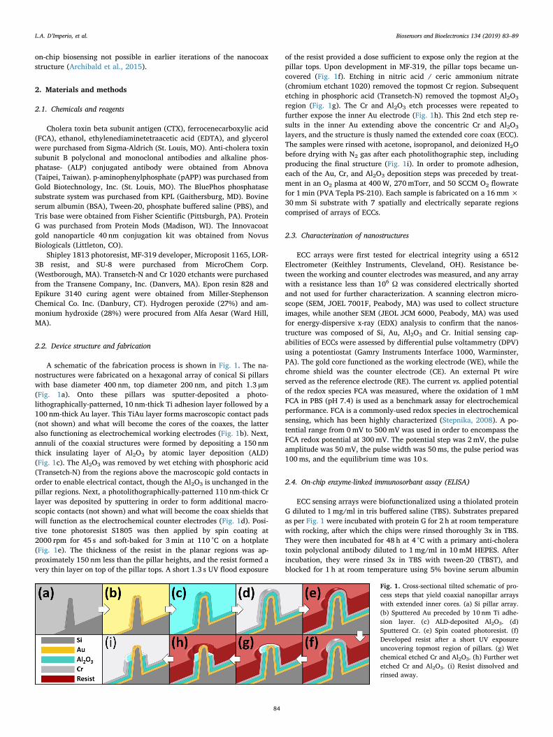
We further explored a number of modifications at several steps infabrication parameters in order to develop the final protocol shown inFigs. 1 and 2. For example, we explored fabricating devices on severaldifferent-shaped silicon arrays (Supplementary information Fig. S1),and identified a core electrode shape that provided both a high level ofreproducibility and a high manufacturing yield. We next focused onmodifications to the etching steps involved in forming the extendedcore (Fig. 2e and f). The effects of all changes were gauged by FCAredox performance and compared against the non-ECC devices andplanar Au electrodes, in order to maximize sensitivity. Computer si-mulations performed in COMSOL Multiphysics were used to informdesign changes. As an example, Fig. 3a and b show the normalizedelectric field distribution corresponding to different shield heights forthe nanocoax. The greater penetration of the Au WE into the highelectric field region suggested that extended core configurations wouldfacilitate higher current response and device sensitivity, which wascorroborated by FCA (1mM) redox data (Fig. 3c). Based on thesefindings, we finalized our ECC architecture as a chip containing 7 in-dividually-addressed sensing arrays, each array comprised of ~30,000nanocoaxes connected in parallel. The measured electrochemical cur-rent in response to 1mM FCA oxidation of these arrays demonstrated ahigh level of experimental reproducibility i.e., ~9% variation in peakcurrent over 9 consecutive measurements (Supplementary informationFig. S2a). This consistency was not achievable on previous nanocoaxes,which exhibited a drop in peak FCA oxidation current in each sub-sequent run until finally stabilizing at a significantly lower current(likely because of liquid exchange issues) (Supplementary informationFig. S2b). Variation in peak current between independently fabricatedECCs is larger than that in repeated measurements on an individualsensing region (Supplementary information, Fig. S2c). It should benoted that this variation does not affect an individual region's viabilityand that the important metric for detection is a region's response to 4-AP redox, which falls in the nA range. Thus, to overcome any potentialissues resulting from the variability of individually fabricated chips, abaseline of 1 μA current in response to FCA oxidation was established tobe the minimum acceptable performance. This corresponds to ~20 μA/mm2 current density, which is also comparable to that used for the non-ECC (Archibald et al., 2015).
Fig. 4a shows a comparison of the peak current density achieved on3 sensing platforms: a simple planar electrode, the non-ECC, and theECC nanocoax. It is apparent from the results that the ECC represents asignificant improvement over its predecessor, as well as over simpler tofabricate architectures lacking a nanogap.
3.2. ECCs as biosensors
3.2.1. Off-chip ELISAAfter fabrication optimization and confirmation of electrochemical
function, ECCs were evaluated for their biosensing capabilities andcompared to the non-ECC version. Non-ECCs had previously been usedto detect CTX in an off-chip setup; in other words, all ELISA steps wereperformed in a 96 well microtiter plate and only the final redox productwas applied to the chip surface for detection. As a baseline for com-parison of the non-ECC and the ECC as biosensors, an off-chip elec-trochemical ELISA was performed. CTX was chosen as the biomarker ofinterest due to its clinical relevance and overall stability. The off-chip
ELISA was performed identically on the ECC and non-ECC, and in turnwas identical to a standard optical ELISA, with the exception of thereadout. For the electrochemical ELISA, pAPP was added as the enzy-matic substrate as opposed to Bluephos for the optical readout. The
Fig. 3. Cross-sectional view of geometry with overlaid simulated electric fieldnorm for 1 V applied to coaxial terminals for the (a) high shield configurationand (b) the low shield configuration (simulated in COMSOL). Inset linear colorscale ranges from 0 V/m (blue) to 2×10⁵ V/m (red) and inset white scale bar is1 µm. (c) DPV current response of oxidizing 1mM FCA comparing the twoshield configurations (3 runs each) shows that the electric field distribution ofthe low shield results in a 4x relative increase in the current response, a metricof sensitivity. (For interpretation of the references to color in this figure legend,the reader is referred to the web version of this article).
L.A. D’Imperio, et al. Biosensors and Bioelectronics 134 (2019) 83–89
86

current response of the ECC off-chip ELISA (Fig. 4b) was superior tothat of the non-ECC (100 pg/ml vs. 2 ng/ml). The ECC demonstrated alinear sensitivity range between 0.1 and 100 ng/ml. An optical ELISAutilizing the same antibodies was capable of detecting as low as 1 ng/mlof CTX, meaning the ECC outperformed this clinical standard. Whencurrent density was taken into account, the ECC vastly outperformedthe non-ECC, as the ECC sensing area was significantly smaller than thatof the non-ECC (0.049mm2 vs. 1.8mm2) (Fig. 4c).
3.2.2. On-chip biofunctionalizationProtein G was utilized to facilitate antibody tethering to the ECC
surface. This is a bacterially-derived protein with a high affinity and
specificity for the Fc region of IgGs (Björck and Kronvall, 1984; Sjöbringet al., 1991). For the purposes herein, it was modified with a thiolgroup, in order to also facilitate binding with a gold surface (Pensaet al., 2012). We first obtained visual (SEM) proof-of-concept of te-thering by conjugating a 40 nm gold nanoparticle to our tertiary ELISAantibody (Supplementary information Fig. S3). These results confirmedbiofunctionalization of the gold core of the ECC with an IgG. We nextsought to complete a full on-chip ELISA on the ECC. Our results de-monstrate on-chip detection of CTX by an ECC functionalized withprotein G (Fig. 5).
4. Discussion
The ECC device was developed in response to architectural con-straints that prevented adequate fluid exchange within the annulus ofthe nanocoax. In order to enable on-chip biofunctionalization, we fab-ricated the ECC to have a gold core that extended outside of the shield,which would be highly available to reagents, and allow for easywashing. The resulting ECC demonstrated a significant increase insensitivity to FCA redox compared to prior generations of nanocoax,and to a planar control electrode.
The increase in current density, which nanocoax architectures ex-hibit over planar electrodes, may be explained by the phenomenon ofredox cycling. Redox cycling occurs between nanogap electrodes,where a species in oxidized at the WE, then reduced at the proximateCE, where it can then rapidly diffuse back to the proximate WE to beoxidized again (Wolfrum et al., 2016; White and McKelvey, 2018).Improvement in signal can be obtained by decreasing the size of theannulus gap that, in turn, may allow for faster redox cycling (Rizalet al., 2013), though eliminating electrical shorting for sub-100 nmannuli needs to be addressed. A simple planar gold electrode withmillimeter-to-centimeter scale distances between electrodes cannotmatch the sensitivity because this cycling does not occur, and thussensitivity is dominated by the rate of reagent diffusion to the electrodesurface.
As both nanocoaxial architectures contain nanogap electrodes, theincrease in current density that the ECC exhibits over the non-ECC maybe explained by the ease of liquid exchange. In order to interact withthe WE it will be necessary for liquid reagents to diffuse into the
Fig. 4. Electrochemical comparisons of the ECC vs. planar and non-ECC ar-chitectures. (a) The average current density resulting from the detection of theoxidation of 1mM FCA is shown for a representative ECC array, a non-ECCarray and a planar gold electrode. (b) Current as a function of applied potentialfor electrochemical ELISAs performed off-chip for CTX concentrations rangingfrom 100 pg/ml to 10 μg/ml, analyzed on the ECC. All measurements weremade on the same ECC array to minimize variability. (c) Peak ELISA currentdensity as a function of CTX concentration, measured on an ECC chip and a non-ECC chip, showing both increased response and lower limit-of-detection for theECC configuration. All error bars represent the standard deviation of 3 trials.
Fig. 5. Current response as a function of applied voltage for ECCs in on-chipdetection of CTX, using protein G to tether antibodies to the sensor surface.Shown are one trial for each condition of 500 ng/ml (red, solid) and 100 ng/ml(blue, dash) concentrations alongside a control sample with no CTX (green).Each trial was performed on a separate array on the same ECC chip. Data weresubtracted to a baseline at −200mV to better show peak current. Deviationsfrom −100mV for the 4-AP oxidation peak are likely due to the use of apseudo-reference electrode. (For interpretation of the references to color in thisfigure legend, the reader is referred to the web version of this article).
L.A. D’Imperio, et al. Biosensors and Bioelectronics 134 (2019) 83–89
87

annulus gap of the non-extended core nanocoax. In actuality, highsurface tension and morphology-induced hydrophobicity caused by thesize of the gap hindered this, and additionally made it difficult to washthe chip surface for further reagent application. By contrast, the ECCWE extends into the solution and so it may be easier for FCA and 4-APmolecules to move from the bulk solution to the electrode surface to beoxidized.
The ECC demonstrated a greater sensitivity toward CTX than anoptical ELISA, with the ECC detecting at 100 pg/ml in an off-chipformat vs. 1 ng/ml for optical. However, the ECC holds the potential tobe functionalized, allowing for all detection steps to be performed on aminiaturized platform, making it a more portable and lower-cost al-ternative to an optical ELISA. This is because the nanocoax deviceachieves its sensitivity while requiring significantly less analyte (aslittle as 10-5 as much) compared to macroscopic optical ELISAs, low-ering the cost per assay. Based on this, we suggest the ECC is a pro-mising architecture for further development toward fully on-chip bio-marker detection. We have established preliminary on-chip detection,but future experiments, including measuring a broader range of CTXconcentrations with the on-chip configuration, are needed to fully va-lidate the ECC architecture as a clinically-viable candidate for a POCdiagnostic tool.
As it stands, however, the current device is competitive with na-nogap devices reported in literature (Table 1). Once full on-chip cap-abilities are confirmed, the ECC will represent a promising alternativeto simpler, planar nanogap-style electrodes because of the increase infunctionalizable surface area resulting from the number of coaxes ineach array, and their 3D architecture. We also believe that the protein Gbiofunctionalization assay represents a much simpler method of anti-body tethering than those frequently used in the literature, such as si-lane or cysteamine functionalization.
Another important feature of the ECC is its amenability to repeateduse. The non-ECC chips exhibited signal degradation over the course ofseveral uses. Conversely, ECC chips maintained signal integrity withless than 10% change in response over 9 runs, suggesting that the ECCsare relatively stable structures. Taken together, these data confirm thatthe ECC represents a significant improvement over the non-ECC ar-chitecture. However, while we have demonstrated the ECC's capabilityof consistent repeated use for measurements that are solely chemicaldetection, e.g., in FCA and 4-AP tests, it is important to note that eachECC sensing region is currently used for a single on-chip detectionassay. The regeneration of biosensing devices has shown promise forenabling repeated use, thereby potentially reducing diagnostic costs,although only a third of reported electrochemical biosensor studiesmeet previously-reported criteria (Goode et al., 2015). To forgo thisproblem, we made 7 separate submillimeter size sensing regions on anindividual sample, thereby achieving the same end-of-line benefit assample regeneration. Furthermore, the number of sensing regions couldbe increased beyond 7, as each region is less than 0.1% of the activesample area.
Lastly, in order for the benefits of such a biosensing device to berelevant to diagnostic applications, it must be affordable in order to
meet the demands of the resource-limited areas where diseases likecholera are most prevalent. Several aspects of the ECC facilitate thiscriterion. The photolithographic processes involved in patterning eachlayer are amenable to large wafer-scale throughput. The chemical wetetching processes are high-throughput, while the chemicals are in-expensive and can be reused for extended periods, given the nanoscopicamount of material etched. Multiple sensing regions on a given chip, aspreviously discussed, can further reduce a sample's cost per test. Sipillar arrays used herein can be easily and inexpensively replicated inpolymer (e.g. SU8) by nanoimprint lithography (NIL). As an electro-chemical sensor, detection using an ECC is performed with equipmentthat is less expensive than that used in standard optical ELISA. As such,further reduction of electrochemical equipment cost is possible by in-corporation of inexpensive microcontroller units such as Arduino.
5. Conclusions
We have demonstrated that an extended core nanocoax is capable ofsensitive and repeatable detection of a target antigen in an off-chipsetup with a detection limit of 100 pg/ml, with preliminary data sug-gesting it possesses utility as an on-chip electrochemical biosensor. Wehave demonstrated that the ECC architecture is a viable and promisingalternative to the non-ECC nanocoax architecture. Future directionsmay include examining more coax core pillar shapes to further improvedevice sensitivity. We have demonstrated that the ECC fabrication iscomprised of processes and chemicals that are suitable for high-throughput, and future works will target these advantages in order tofurther decrease the cost per sample. Future works will also include thefabrication of a more sophisticated chip housing that incorporates mi-crofluidics and a portable analysis system in order to enable the ECC'suse for POC detection of infectious disease biomarkers, offering thepotential to meet the diagnostic needs of resource-limited areas.
Acknowledgements
The authors thank Steve Shepard in the Boston College IntegratedScience Clean Room Facility for advice and assistance in device fabri-cation, Richard Pijar for assistance making and repairing electroniccomponents for experiments, and Roger J. Fleischmann for technicalsupport.
Declaration of interest statement
All authors certify that they have no affiliations with or involvementin any organization or entity with any financial interest, or non-fi-nancial interest in the subject matter or materials discussed in thismanuscript.
Author contributions
A.E. Valera planned the study, performed experiments related tobiological detection, analyzed results and co-wrote the original draft of
Table 1A comparison of nanogap-based protein detection platforms.
Citation Biomarker Lowest concentration detected (ng/ml) Recognition scheme Transduction
Current device Cholera toxin subunit B 0.1 (off chip) Thiolated protein G antibody tethering DPV100 (on chip)
(Singh et al., 2010) C reactive protein 0.1 Cysteamine SAM EIS(Hsueh and Lin, 2016) Cardiac-troponin T 0.1 Silane functionalization CV(Ilyas et al., 2012) Epidermal growth factor receptor 50 Immobilized aptamer Impedance(Whited et al., 2012) HE4 Biomarker 1.5 (standalone) Cysteamine SAM EIS
0.1 (mixed)(Kim et al., 2009) Prostate specific antigen 0.0001 Protein G antibody tethering Electrical(Carlo and Lee, 2003) Laminin 10 Silane funcitonalization Capacitive
L.A. D’Imperio, et al. Biosensors and Bioelectronics 134 (2019) 83–89
88

the manuscript. L.A. D’Imperio optimized ECC design, fabricated alldevices, performed quality control, and co-wrote the original draft ofthe manuscript. J.R. Naughton established the ECC fabrication metho-dology. M.M. Archibald developed the initial off-chip ELISA metho-dology. J.M. Merlo provided scientific supervision in the fabrication ofdevices. T.J. Connolly and M.J. Burns provided scientific supervision asexperts in biology and physics. T.C. Chiles co-supervised experiments.M.J. Naughton conceptualized the ECC design, provided scientific su-pervision and laboratory equipment for analysis, and co-conceived ofthe original nanocoaxial architecture. All authors also reviewed andedited the manuscript.
Appendix A. Supplementary material
Supplementary data associated with this article can be found in theonline version at doi:10.1016/j.bios.2019.03.045.
References
Archibald, M.M., Rizal, B., Connolly, T., Burns, M.J., Naughton, M.J., Chiles, T.C., 2015.A nanocoaxial-based electrochemical sensor for the detection of cholera toxin.Biosens. Bioelectron. 74, 406–410. https://doi.org/10.1016/j.bios.2015.06.069.
Arroyo-Currás, N., Scida, K., Ploense, K.L., Kippin, T.E., Plaxco, K.W., 2017. High surfacearea electrodes generated via electrochemical roughening improve the signaling ofelectrochemical aptamer-based biosensors. Anal. Chem. 89, 12185–12191. https://doi.org/10.1021/acs.analchem.7b02830.
Björck, L., Kronvall, G., 1984. Purification and some properties of streptococcal protein G,a novel IgG-binding reagent. J. Immunol. 133, 969–974. https://doi.org/10.1385/1-59259-076-4:281.
Brazaca, L.C., Ribovski, L., Janegitz, B.C., Zucolotto, V., 2017. Nanostructured materialsand nanoparticles for point of care (POC) medical biosensors. Med. Biosens. PointCare Appl. 229–254. https://doi.org/10.1016/B978-0-08-100072-4.00010-1.
Carlo, C.D., and, Lee, L.P., 2003. Nanogap-based dielectric immunosensing, In:Transducers ’03. Proceedings of the 12th International Conference on Solid-StateSensors, Actuators and Microsystems. Digest of Technical Papers (Cat. No.03TH8664), pp. 1180–1183 vol.2. ⟨http://dx.doi.org/10.1109/SENSOR.2003.1216982⟩.
Chen, X., Guo, Z., Yang, G.M., Li, J., Li, M.Q., Liu, J.H., Huang, X.J., 2010. Electricalnanogap devices for biosensing. Mater. Today 13, 28–41. https://doi.org/10.1016/S1369-7021(10)70201-7.
Erickson, H.P., 2009. Size and shape of protein molecules at the nanometer level de-termined by sedimentation, gel filtration, and electron microscopy. Biol. Proced.Online 11, 32–51. https://doi.org/10.1007/s12575-009-9008-x.
Feng, Y., Zhang, Y., Ying, C., Wang, D., Du, C., 2015. Nanopore-based fourth-generationDNA sequencing technology. Genom. Proteom. Bioinforma. 13, 4–16. https://doi.org/10.1016/j.gpb.2015.01.009.
Goode, J.A., Rushworth, J.V.H., Millner, P.A., 2015. Biosensor regeneration: a review ofcommon techniques and outcomes. Langmuir 31, 6267–6276. https://doi.org/10.1021/la503533g.
Grieshaber, D., MacKenzie, R., Vörös, J., Reimhult, E., 2008. Electrochemical biosensors -Sensor principles and architectures. Sensors. https://doi.org/10.3390/s8031400.
Hsueh, H.-T., Lin, C.-T., 2016. An incremental double-layer capacitance of a planar nanogap and its application in cardiac-troponin T detection. Biosens. Bioelectron. 79,636–643. https://doi.org/10.1016/j.bios.2015.12.105.
Ilyas, A., Asghar, W., Allen, P.B., Duhon, H., Ellington, A.D., Iqbal, S.M., 2012. Electricaldetection of cancer biomarker using aptamers with nanogap break-junctions.Nanotechnology 23, 275502. https://doi.org/10.1088/0957-4484/23/27/275502.
Kasemo, B., 1998. Biological surface science. Curr. Opin. Solid State Mater. Sci. 3,451–459. https://doi.org/10.1016/S1359-0286(98)80006-5.
Kim, S.K., Cho, H., Park, H.-J., Kwon, D., Lee, J.M., Chung, B.H., 2009. Nanogap bio-sensors for electrical and label-free detection of biomolecular interactions.Nanotechnology 20, 455502. https://doi.org/10.1088/0957-4484/20/45/455502.
Li, T., Hu, W., Zhu, D., 2010. Nanogap electrodes. Adv. Mater. 22, 286–300. https://doi.org/10.1002/adma.200900864.
Liu, S., Wang, Z., Wang, F., Yu, B., Zhang, T., 2014. High surface area mesoporous CuO: a
high-performance electrocatalyst for non-enzymatic glucose biosensing. RSC Adv. 4,33327–33331. https://doi.org/10.1039/c4ra04700a.
Lowe, C.R., 1984. Biosensors. Trends Biotechnol. 2, 59–65. https://doi.org/10.1016/0167-7799(84)90011-8.
MacKay, S., Hermansen, P., Wishart, D., Chen, J., 2015. Simulations of interdigitatedelectrode interactions with gold nanoparticles for impedance-based biosensing ap-plications. Sensors (Switz.) 15, 22192–22208. https://doi.org/10.3390/s150922192.
Merlo, J.M., Ye, F., Rizal, B., Burns, M.J., Naughton, M.J., 2014. Near-field observation oflight propagation in nanocoax waveguides. Opt. Express 22, 14148. https://doi.org/10.1364/OE.22.014148.
Morgan, D.M., Weber, S.G., 1984. Noise and signal-to-noise ratio in electrochemical de-tectors. Anal. Chem. 56, 2560–2567. https://doi.org/10.1021/ac00277a065.
Naughton, J.R., Connolly, T., Varela, J.A., Lundberg, J., Burns, M.J., Chiles, T.C.,Christianson, J.P., Naughton, M.J., 2016. Shielded coaxial optrode arrays for neu-rophysiology. Front. Neurosci. 10, 1–10. https://doi.org/10.3389/fnins.2016.00252.
Naughton, M.J., Kempa, K., Ren, Z.F., Gao, Y., Rybczynski, J., Argenti, N., Gao, W., Wang,Y., Peng, Y., Naughton, J.R., McMahon, G., Paudel, T., Lan, Y.C., Burns, M.J.,Shepard, A., Clary, M., Ballif, C., Haug, F.J., Söderström, T., Cubero, O., Eminian, C.,2010. Efficient nanocoax-based solar cells. Phys. Status Solidi - Rapid Res. Lett. 4,181–183. https://doi.org/10.1002/pssr.201004154.
Otero, T.F., Martinez, J.G., Asaka, K., 2016. Faradaic and capacitive components of theCNT electrochemical responses. Front. Mater. 3, 1–11. https://doi.org/10.3389/fmats.2016.00003.
Pensa, E., Cortés, E., Corthey, G., Carro, P., Vericat, C., Fonticelli, M.H., Benítez, G.,Rubert, A.A., Salvarezza, R.C., 2012. The chemistry of the sulfur-gold interface: Insearch of a unified model. Acc. Chem. Res. 45, 1183–1192. https://doi.org/10.1021/ar200260p.
Purohit, P.K., Inamdar, M.M., Grayson, P.D., Squires, T.M., Kondev, J., Phillips, R., 2005.Forces during bacteriophage DNA packaging and ejection. Biophys. J. 88, 851–866.https://doi.org/10.1529/biophysj.104.047134.
Rizal, B., Archibald, M.M., Connolly, T., Shepard, S., Burns, M.J., Chiles, T.C., Naughton,M.J., 2013. Nanocoax-based electrochemical sensor. Anal. Chem. 85, 10040–10044.https://doi.org/10.1021/ac402441x.
Roy, S., Gao, Z., 2009. Nanostructure-based electrical biosensors. Nano Today 4,318–334. https://doi.org/10.1016/j.nantod.2009.06.003.
Rybczynski, J., Kempa, K., Herczynski, A., Wang, Y., Naughton, M.J., Ren, Z.F., Huang,Z.P., Cai, D., Giersig, M., 2007. Subwavelength waveguide for visible light. Appl.Phys. Lett. 90. https://doi.org/10.1063/1.2430400.
Shim, J.S., Rust, M.J., Ahn, C.H., 2013. A large area nano-gap interdigitated electrodearray on a polymer substrate as a disposable nano-biosensor. J. Micromech.Microeng. 23. https://doi.org/10.1088/0960-1317/23/3/035002.
Singh, K.V., Whited, A.M., Ragineni, Y., Barrett, T.W., King, J., Solanki, R., 2010. 3Dnanogap interdigitated electrode array biosensors. Anal. Bioanal. Chem. 397,1493–1502. https://doi.org/10.1007/s00216-010-3682-z.
Sjöbring, U., Björck, L., Kastern, W., 1991. Streptococcal protein G. J. Biol. Chem. 266,399–405. https://doi.org/10.1099/mic.0.039578-0.
Stepnika, P., 2008. Ferrocenes: Ligands, Materials and Biomolecules. Wiley.White, H.S., McKelvey, K., 2018. Redox cycling in nanogap electrochemical cells. Curr.
Opin. Electrochem. 7, 48–53. https://doi.org/10.1016/J.COELEC.2017.10.021.Whited, A.M., Singh, K.V., Evans, D., Solanki, R., 2012. An electronic sensor for detection
of early-stage biomarker/s for ovarian cancer. BioNanoSci 2, 161–170. https://doi.org/10.1007/s12668-012-0049-2.
Wolfrum, B., Kätelhön, E., Yakushenko, A., Krause, K.J., Adly, N., Hüske, M., Rinklin, P.,2016. Nanoscale electrochemical sensor arrays: redox cycling amplification in dual-electrode systems. Acc. Chem. Res. 49, 2031–2040. https://doi.org/10.1021/acs.accounts.6b00333.
Wongkaew, N., Simsek, M., Griesche, C., Baeumner, A.J., 2018. Functional nanomaterialsand nanostructures enhancing electrochemical biosensors and lab-on-a-chip perfor-mances: recent progress, applications, and future perspective. Chem. Rev. https://doi.org/10.1021/acs.chemrev.8b00172.
Zhang, S., Geryak, R., Geldmeier, J., Kim, S., Tsukruk, V.V., 2017. Synthesis, assembly,and applications of hybrid nanostructures for biosensing. Chem. Rev. 117,12942–13038. https://doi.org/10.1021/acs.chemrev.7b00088.
Zhao, H., Rizal, B., McMahon, G., Wang, H., Dhakal, P., Kirkpatrick, T., Ren, Z., Chiles,T.C., Naughton, M.J., Cai, D., 2012. Ultrasensitive chemical detection using a na-nocoax sensor. ACS Nano 6, 3171–3178. https://doi.org/10.1021/nn205036e.
Zhu, C., Yang, G., Li, H., Du, D., Lin, Y., 2015. Electrochemical sensors and biosensorsbased on nanomaterials and nanostructures. Anal. Chem. 87, 230–249. https://doi.org/10.1021/ac5039863.
L.A. D’Imperio, et al. Biosensors and Bioelectronics 134 (2019) 83–89
89

1
SUPPLEMENTARY MATERIALS DOCUMENT
An extended core nanocoax pillar architecture for enhanced molecular detection
L.A. D’Imperio*, A.E. Valera*, J.R. Naughton, M.M. Archibald, J.M. Merlo, T.J. Connolly,
M.J. Burns, T.C. Chiles, and M.J. Naughton
* These authors contributed equally to this work.
Abstract
Biosensors that incorporate nanomaterials and nanofabrication techniques enable
molecular detection of chemical and biological macromolecules with a high degree of specificity
and ultrasensitivity. Here, we present a novel fabrication process that yields a nanostructure
capable of detecting biological macromolecules. The extended core nanocoax structure builds on
a previously reported nanocoaxial-based sensor. The fabrication of the device incorporates an
extended inner pillar, with controllable extension above the annulus and into the surrounding
solution. This new design eliminates structural constraints inherent in the original nanocoax
architecture. We also provide results demonstrating improvement in biosensing capability.
Specifically, we show the capability of the new architecture to detect the B subunit of the Vibrio
cholerae toxin at improved sensitivity in comparison to optical enzyme-linked immunosorbant
assay and the previously reported coaxial nanostructures.
Keywords
Nanocoax, nanofabrication, extended-core, biosensor, high-sensitivity, ELISA

2
Supplementary Figures
Supp. Fig. 1. Several types of Si pillar arrays were evaluated. FCA electrochemical results, in
addition to the availability of chips, dictated the shape used for final testing. Slightly conical-
shaped Si pillars (a) were chosen for further work. Sharp (b), cylindrical (c), and high-aspect
ratio (d) pillars did not provide sufficient electrical and electrochemical consistency for further
use. Scale bar inset is 1 μm for (a-c) and 2 μm for (d). SEM images taken at 30o tilt. Si substrates
were imaged with a layer of Au deposited in order to reduce image distortion due to charge
accumulation.

3
Supp. Fig. 2. Measured current density of (a) non-ECC and (b) ECC arrays for multiple repeated
runs on the same region. The peak current density for non-ECC drops off quickly for subsequent
runs, whereas for ECC, it shows high repeatability over 9 runs. Note the different axis ranges
used. (c) Peak current and standard deviation from 6 separate sensing regions, each from
independently-fabricated ECC samples.

4
Supp. Fig. 3. SEM images of the extended core nanocoax. SEMs of two separate arrays on the
same ECC chip, (a) one incubated without protein G (- Protein G), and (b) one with protein G
(Protein G), both prior to AuNP-conjugated antibody application. Corresponding 30° tilted
views are shown in (c) and (d), respectively. AuNPs of ~40 nm diameter are visible around the
extended cores of the test array (+ Protein G), but not the control array (-Protein G). Note that a
particular iteration of ECC was utilized in this study, expected to be representative of the
behavior of all ECC chips. Inset scale bar is 1µm in length.

5
Supp. Fig. 4. Picture of a 16 mm x 30 mm final sample with 7 separate sensing regions. Inset
image is a x100 magnification of an individual sensing region, showing the leads for the inner
(Au) and outer (Cr) electrodes converging to the circular nanocoax array.


![Biosensors & Bioelectronics - OMICS International | Open … · Biosensors & Bioelectronics ... Mi-Kyung Park, Materials Research and Education Center, ... [18]. E2 phage was provided](https://static.fdocuments.net/doc/165x107/5acd99ae7f8b9a93268dcd3a/biosensors-bioelectronics-omics-international-open-bioelectronics-mi-kyung.jpg)