
Basic Electrical & Electronics - Indian Railways
298
Phase I - Module No. FC-03
Transcript of Basic Electrical & Electronics - Indian Railways

Phase I - Module No. FC-03

Basic Electrical & Electronics
1. Various terms, units, theory of passive components – L,C,R, basic principle of electricity and Electromagnetic induction and various law i.e. Ohm’s law, Kirchoff’s law, etc.
2. Classification of electronics components, Active Components, Semiconductor physics, construction and operating principle.
3. Brief on Power Diodes, Zener diodes, LEDs, BJTs, UJT, MOSFET, SCR, GTO and IGBT etc.
4. Practical work on – oscilloscopes, testing of passive electronics components, Testing of active components.

Basic Electrical & Electronics
I. Various terms,
II. Units,
III. Theory of passive components – L,C,R,
IV. Basic principle of electricity and
V. Electromagnetic induction and
VI. Various law i.e. Ohm’s law,
VII. Kirchoff’s law,etc.

Module No. Brief Description Duration
FC 03
Basic Electrical & Electronicsa. Various terms, units, theory of passive
components – L,C,R, basic principle of electricity and Electromagnetic induction and various law i.e. Ohm’s law, Kirchoff’slaw, etc.
b. Classification of electronics components, Active Components, Semiconductor physics, construction and operating principle.
c. Brief onPower Diodes,Zenerdiodes,LEDs,BJTs,UJT,MOSFET,SCR,GTOand IGBT etc.
d. Practical work on –oscilloscopes, testing of passive electronics components, Testing of active components.
6 Days

Various terms & units

• Ambient Temperature
• Temperature of the air surrounding a component.
• Ampere
• Ampere(s), the unit of electrical current. Current is defined as the amount of charge that flows past a give point, per unit of time.
• The symbol I is used for current in equations and A is the abbreviation for ampere.
Terms & Units

• Ampere-hour• A measure of charge (or current flow over time).
• One ampere-hour (or amp-hour or Ah) is a current of one ampere flowing for one hour. The amount of charge transferred in that hour is 3,600 coulombs (ampere-seconds).
• A milliampere-hour (mAh or milliamp-hour) is a thousandth of an amp-hour.
• An ampere-second (A-s or amp-second) is an amp supplied for one second.
Terms & Units

• mA
• Milliampere, or milliamp: 1/1000 of an Ampere. Ampere is the basic unit for measuring electrical current.
• pF
• Picofarad. A Farad is the unit of capacitance. A pF is 10-12 of a Farad. (1000pF = 1nF, 1000nF = 1 microfarad).
Terms & Units

• Volt
• Volt (or Volts): Unit of measure for electromotiveforce (EMF), the electrical potential between twopoints. An electrical potential of 1 volt will push 1ampere of current through a 1-ohm resistive load.
• In equations, the symbol E is often used (as in: E =IR). V is the symbol for the unit of measure, Volt.
Terms & Units

• Volt-Ampere
• A volt-ampere (VA) is the voltage times the current feeding an electrical load. A kilovolt-ampere (kVA) is 1000 volt-amperes.
• Electrical power is measured in watts (W): The voltage times the current measured each instant. In a direct current system or for resistive loads, the wattage and VA measurements will be identical. But for reactive loads, the voltage and current are out of phase and the volt-ampere spec will be greater than the wattage.
Terms & Units

• Joule
• Joule (abbreviated J): A measurement of energy or work. In mechanical systems, it's the a force of one newton, moving an object a distance of one meter.
• In electronics, it's the same amount of energy, in electrical units. One joule is one watt of power, applied for one second (a watt-second); or a coulomb of electrical charge raised to a potential of one volt.
Terms & Units
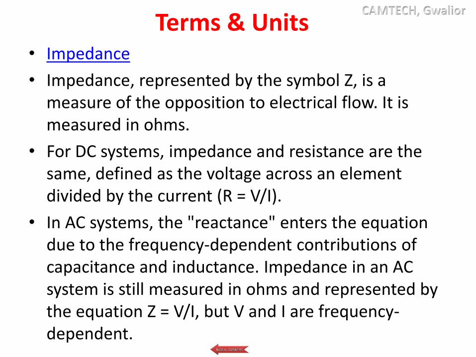
• Impedance
• Impedance, represented by the symbol Z, is a measure of the opposition to electrical flow. It is measured in ohms.
• For DC systems, impedance and resistance are the same, defined as the voltage across an element divided by the current (R = V/I).
• In AC systems, the "reactance" enters the equation due to the frequency-dependent contributions of capacitance and inductance. Impedance in an AC system is still measured in ohms and represented by the equation Z = V/I, but V and I are frequency-dependent.
Terms & Units
Basic principle of electricity
and
Electromagnetic induction
and
various law
i.e. Ohm’s law, Kirchoff’s law,etc.

Basic Principle of Electricity

Definition:
Electricity is a form of energy that can be easily changed to other forms.
What is Electricity ??
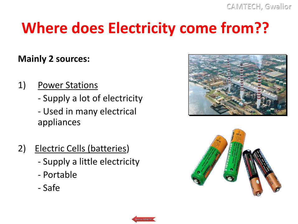
Where does Electricity come from??
Mainly 2 sources:
1) Power Stations
- Supply a lot of electricity
- Used in many electrical appliances
2) Electric Cells (batteries)
- Supply a little electricity
- Portable
- Safe

How does an Electrical Appliance Work??
• To make an electrical appliance work, electricity must flow through it.
• The flow of electricity is called an electric current.
• The path along which the electric current moves is called
the electric circuit.

What is an Electric Current??
Definition - An electric current is the rate of flow of electric charges in a circuit.
connecting
wire
electric
cell
filament
flow of electrons

Electric Charges
• Electric charges are made up of positive charges (protons) and negative charges (electrons).
• When these charges flow in a circuit, a current is
produced.

How does electricity flow??
• The battery in a circuit gives energy to the electrons and pushes them around a circuit, from the negative terminal of the cell, round the circuit and back to the positive terminal of the cell.
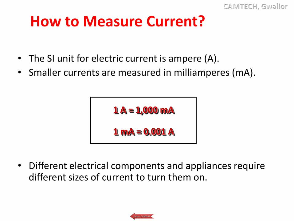
• The SI unit for electric current is ampere (A).
• Smaller currents are measured in milliamperes (mA).
• Different electrical components and appliances require different sizes of current to turn them on.
How to Measure Current?
1 A = 1,000 mA
1 mA = 0.001 A
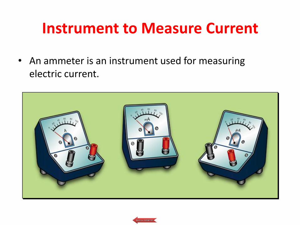
Instrument to Measure Current
• An ammeter is an instrument used for measuring electric current.
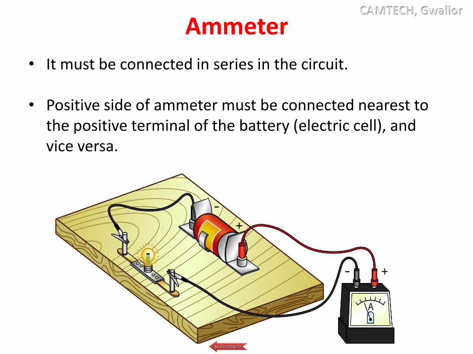
Ammeter
• It must be connected in series in the circuit.
• Positive side of ammeter must be connected nearest to the positive terminal of the battery (electric cell), and vice versa.

Electric Circuits
• Electric circuits are made up of electrical components
• These components must be joined together without any gap in between to form a closed circuit.
connecting wires
electric cell
circuit boardlight bulb
Note:Components refer to the light bulb, wires, battery

Electric Circuits
• Incomplete circuits are called open circuits.
connecting wire is
missing
no source of
electrical energy
Both the circuits in the diagram are incomplete, hence they are known as “open circuits”.
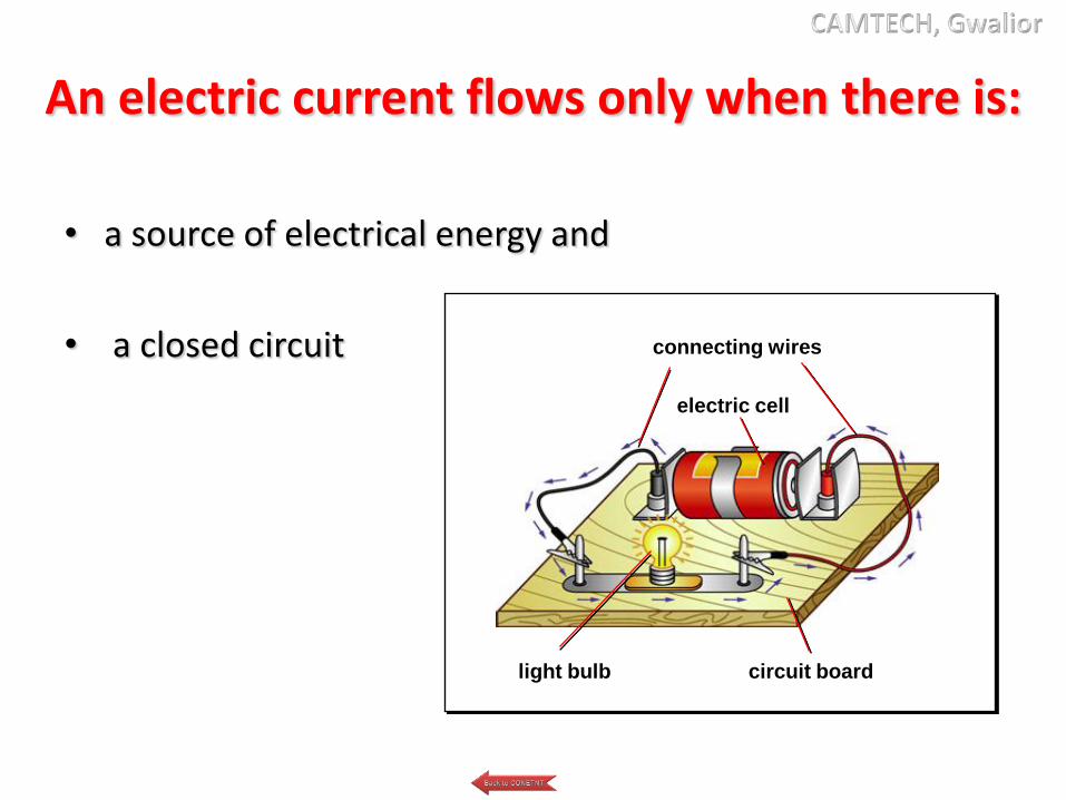
An electric current flows only when there is:
• a source of electrical energy and
• a closed circuit connecting wires
electric cell
circuit boardlight bulb

How to draw Circuit Diagrams
Component Symbol Component Symbol
An electric cell Battery
Light bulb (lamp) Switch
Switch (open)
Switch (closed)
Connecting wires (not joined)
Connecting wires (joined)
+ +
Symbols are used to represent the various electrical components in circuits.

Symbol

Symbol
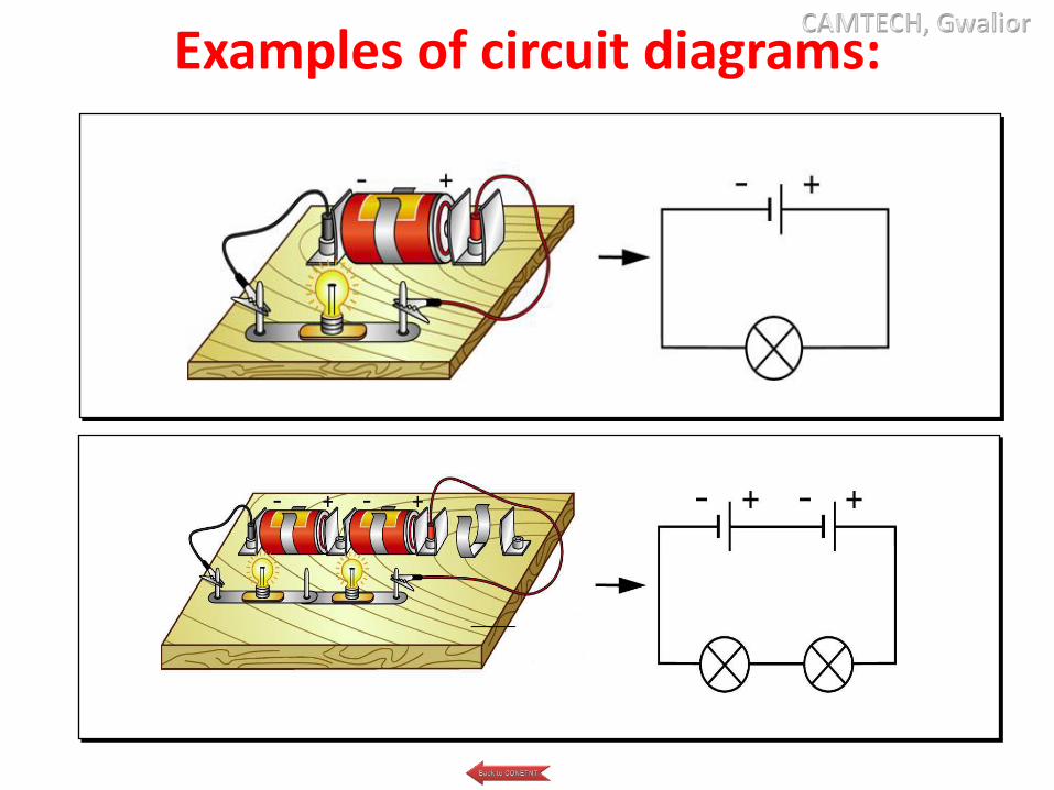
Examples of circuit diagrams:
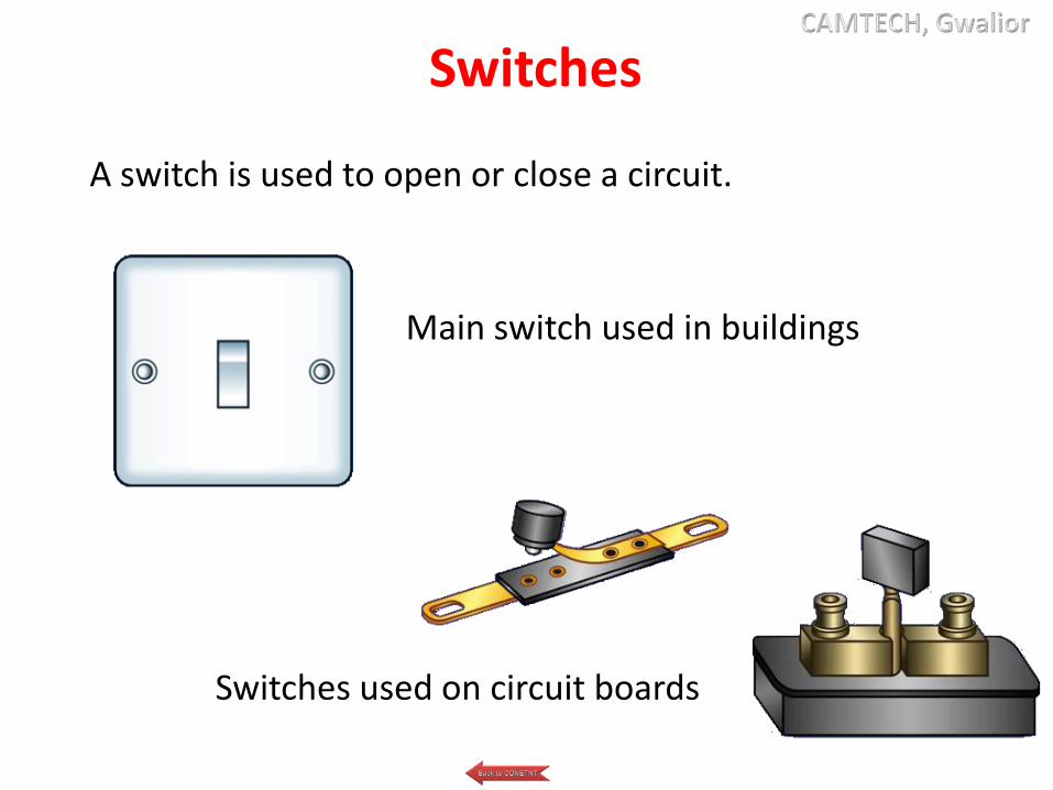
Switches
A switch is used to open or close a circuit.
Main switch used in buildings
Switches used on circuit boards

Circuit diagrams for open and closed circuits
Open circuit -Bulb does not light up when the switch is open.
Close circuit -Bulb will light up when the switch is closed.

Series and Parallel
There are 2 ways in which an electric circuit can be arranged:
1. Series
2. Parallel

Series Circuit
• A series circuit connects the components one after the other.
• A single loop is formed.
• A break in any part of a series circuit stops the flow of current in the whole circuit.
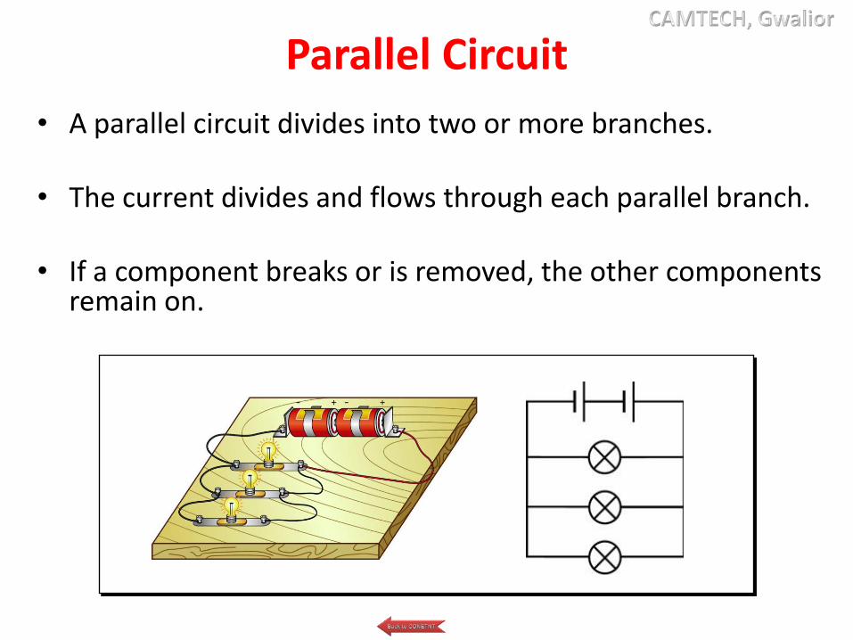
Parallel Circuit
• A parallel circuit divides into two or more branches.
• The current divides and flows through each parallel branch.
• If a component breaks or is removed, the other components remain on.
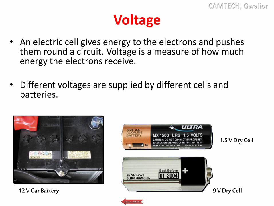
Voltage
• An electric cell gives energy to the electrons and pushes them round a circuit. Voltage is a measure of how much energy the electrons receive.
• Different voltages are supplied by different cells and batteries.
12 V Car Battery
1.5 V Dry Cell
9 V Dry Cell

How to Measure Voltage??
• The SI unit for voltage is volt (V).
• A voltmeter is an instrument used for measuring voltages.

Voltmeter
• Voltmeters must be connected in parallel to the circuit.
• The positive side of voltmeter is connected to the positive terminal of the cell, and vice versa.
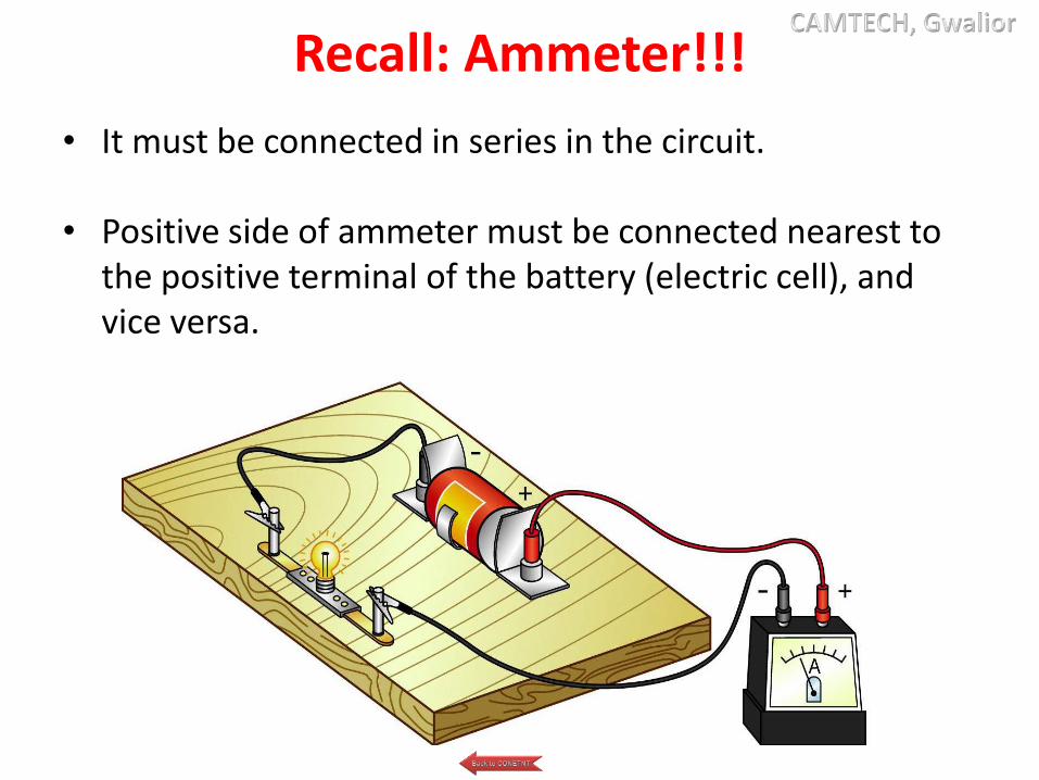
Recall: Ammeter!!!
• It must be connected in series in the circuit.
• Positive side of ammeter must be connected nearest to the positive terminal of the battery (electric cell), and vice versa.

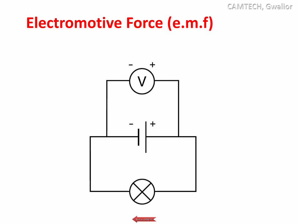
Electromotive Force (e.m.f)
• Electromotive force is the same as voltage.
• E.m.f refers to the amount of energy supplied by the electric source (eg. battery) to each unit of electric charge.
• E.m.f is also measured by a voltmeter
Electromotive Force (e.m.f)

Potential Difference (P.d.)
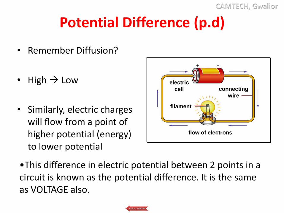
Potential Difference (p.d)
• Remember Diffusion?
• High Low
• Similarly, electric charges will flow from a point of higher potential (energy) to lower potential
connecting
wire
electric
cell
filament
flow of electrons
•This difference in electric potential between 2 points in a circuit is known as the potential difference. It is the same as VOLTAGE also.

Heating Effect of Electric Current
• When an electric current flows through a wire, the wire heats up. Electrical energy has been converted into heat energy.
• The greater the resistance of the wire, the greater the amount of heat produced. This heating effect is used in common electrical appliances.
Iron Kettle Hair Dryer

A kettle uses both copper and nichrome wires.Copper has low resistance while nichrome has high resistance.Which material, copper or nichrome, should be used for the heating element, and for the external wire?
Use copper wire for the external wire as it has low resistance & produces less heat
Use nichrome wire for the heating element as it has high resistance& produces a lot of heat
Heating Effect of Electric Current

Filament wire produces heat and light
In a light bulb, the heated filament which isalso a resistance wire, becomes so hot thatlight is also emitted.
Heating Effect of Electric Current
ARGON (inert/unreactive gas)

Chemical Effect of Electric Current
What is ELECTROLYSIS?
Definition:• Electrolysis is the chemical change that occurs when an
electric current passes through solutions or molten compounds.

Electrolysis
There are 2 uses of electrolysis:
1) Electroplating
2) Extraction of Metals

1. Electroplating
• In electroplating, a key is covered with a thin layer of copper when electricity is passed through the solution.
key copper
wire
copper
sulphate
solutionstart after a few minutes
copper on
the key
- +

2. Extraction of metals
• Some metals (eg. sodium, aluminium) are obtained by electrolysis.
• To extract the metal
– heat the solid compound of the metal until it melts
– pass an electric current through the molten compound

Magnetic Effect of a Current
• A straight wire is placed near a compass. When anelectric current flows through the wire, the compassneedle is deflected. This shows that an electric currenthas a magnetic effect.
compass needle is deflectedcurrent in
wire

Electromagnet
• An electromagnet is a magnet that is made by using electricity
• It consist of a wire coiled around a metal rod (eg. Iron)
coil of wire
to battery
iron core
compass needle is strongly
attracted to iron core

Electromagnet
The magnetic effect of the electromagnet can be increased by :
1. increasing the current (by using more batteries)
2. increasing the number of turns of wire in the coil
3. Using an iron rod

Differences between an electromagnet and a magnet:
Electromagnet Magnet
A temporary magnet which can be turned on and off
using electric current.
A permanent magnet which retains magnetism until it is
purposely demagnetised(spoilt).
Magnet can be made stronger or weaker
Magnet remains the same strength

Uses of Electromagnets
• Cranes that lift iron/steel
• Iron/steel separators
• Electric bells
• Magnetically levitated trains
• Electric motors crane
Electric motor in fans
Electric bell

Electromagnetic Induction

Induced Current
• When a conductor moves across flux lines, magnetic forces on the free electrons induce an electric current.• Right-hand force rule shows current outward for down and inward for up motion. (Verify)
Down I
Down
v
BF
Up v
B
F
Up
I
B
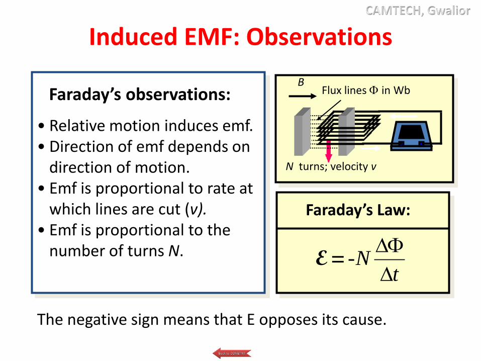
Induced EMF: Observations
BFlux lines F in Wb
N turns; velocity v
Faraday’s Law:
Faraday’s observations:
• Relative motion induces emf.• Direction of emf depends on
direction of motion.• Emf is proportional to rate at
which lines are cut (v).• Emf is proportional to the
number of turns N. -Nt
F
E =
The negative sign means that E opposes its cause.

Magnetic Flux Density
f
Magnetic Flux
density:
ABA
F
• Magnetic flux lines F are continuous and closed.
• Direction is that of the B vector at any point.
; = B BAA
F F
When area A is perpendicular to flux:
The unit of flux density is the weber per square meter.
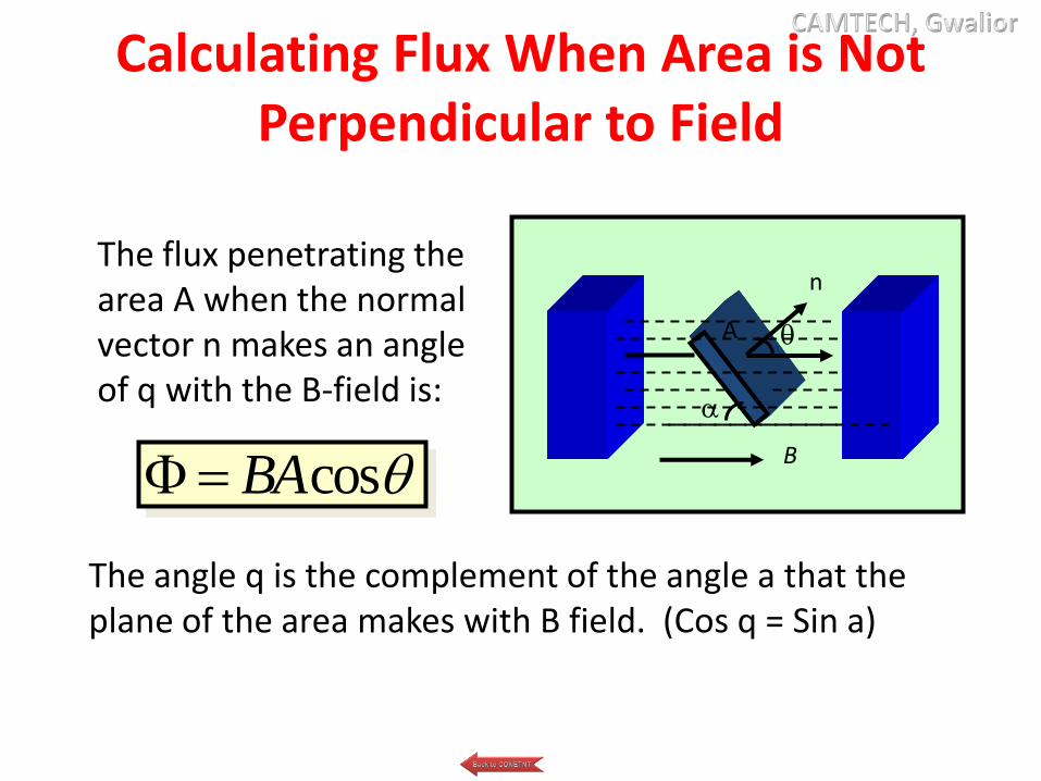
Calculating Flux When Area is Not Perpendicular to Field
The flux penetrating the area A when the normal vector n makes an angle of q with the B-field is:
cosBA F
The angle q is the complement of the angle a that the plane of the area makes with B field. (Cos q = Sin a)
n
A
a
B

Application of Faraday’s Law
Faraday’s Law:
-Nt
F
E =
A change in flux F can occur by a change in area or by a change in the B-field:
F = B A F = A B
n
n
n
Rotating loop = B A Loop at rest = A B
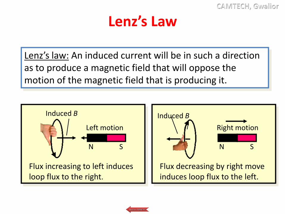
Lenz’s Law
Lenz’s law: An induced current will be in such a direction as to produce a magnetic field that will oppose the motion of the magnetic field that is producing it.
Flux decreasing by right move induces loop flux to the left.
N S
Left motion
Induced B
Flux increasing to left induces loop flux to the right.
N S
Right motionI
Induced B

x x x x x x x x x x xx x x x x x x x x x xx x x x x x x x x x xx x x x x x x x x x xx x x x x x x x x x xx x x x x
Directions of Forces and EMFs
vL
vI
I
x
BI
v
Induced emf
An emf E is induced by moving wire at velocity v in constant B field. Note direction of I.
From Lenz’s law, we see that a reverse field (out) is created. This field causes a leftward force on the wire that offers resistance to the motion. Use right-hand force rule to show this.
x x x xx x xx x xx x xx x xx x
B
I
Lenz’s law
v

Motional EMF in a Wire
L v
I
I
x
x x x x x x x x x x x x x x x x x x x x x x x x x x x x x x x x x x x x x x x x x x x x x x
BF
v
Force F on charge q in wire:
F = qvB; Work = FL = qvBL
Work qvBL
q qE =
EMF: BLvE=
If wire of length L moves with velocity v an angle with B:
Induced Emf E
v sin v
B
sinBLv E=
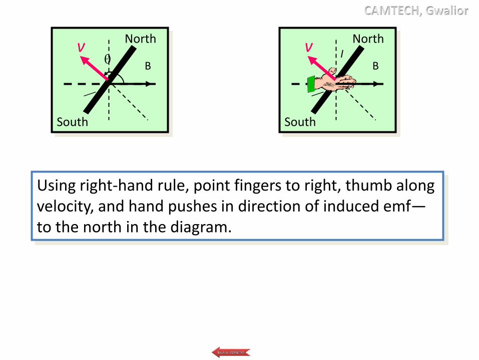
v
B
North
South
Using right-hand rule, point fingers to right, thumb along velocity, and hand pushes in direction of induced emf—to the north in the diagram.
vB
North
South
I

The AC Generator
Rotating Loop in B-field• An alternating AC current is produced by rotating a loop in a constant B-field.
• Current on left is outward by right-hand rule.
• The right segment has an inward current.
• When loop is vertical, the current is zero.
v
B
I
v
B
I
I in R is right, zero, left, and then zero as loop rotates.
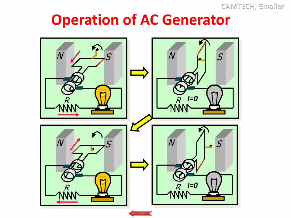
Operation of AC Generator
I=0
I=0

Sinusoidal Current of Generator
The emf varies sinusoidally with max and min emf
+E
-E
sinNBA EFor N turns, the EMF is:
x.
x.

The DC Generator
DC Generator
The simple ac generator can be converted to a dc generator by using a single split-ring commutator to reverse connections twice per revolution.
Commutator
For the dc generator: The emf fluctuates in magnitude, but always has the same direction (polarity).
tE

The Electric Motor
In a simple electric motor, a current loop experiences a torque which produces rotational motion. Such motion induces a back emf to oppose the motion.
Electric Motor
V
V – Eb = IR
Applied voltage – back emf = net voltage
Since back emf Eb increases with rotational frequency, the starting current is high and the operating
current is low: Eb = NBA sin
Eb
I

Armature and Field Windings
In the commercial motor, many coils of wire around the armature will produce a smooth torque. (Note directions of I in wires.)
Series-Wound Motor: The field and armature wiring are connected in series.
Motor
Shunt-Wound Motor: The field windings and the armature windings are connected in parallel.
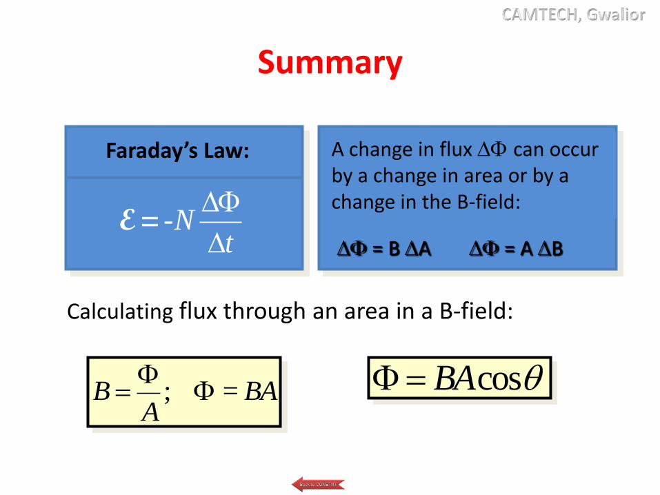
Summary
Faraday’s Law:
-Nt
F
E =
A change in flux F can occur by a change in area or by a change in the B-field:
F = B A F = A B
cosBA F ; = B BAA
F F
Calculating flux through an area in a B-field:

Summary (Cont.)
Lenz’s law: An induced current will be in such a direction as to produce a magnetic field that will oppose the motion of the magnetic field that is producing it.
Flux decreasing by right move induces loop flux to the left.
N S
Left motion
I
Induced B
Flux increasing to left induces loop flux to the right.
N S
Right motionI
Induced B

Summary (Cont.)
sinBLv E= Induced Emf E
v sin v
BAn emf is induced by a wire moving with a velocity v at an angle with a B-field.
sinNBA EFor N turns, the EMF is:
In general for a coil of N turns of area A rotating with a frequency in a B-field, the generated emfis given by the following relationship:

Summary (Cont.)
DC Generator Electric Motor
V
The ac generator is shown to the right. The dc generator and a dc motor are shown below:

Summary (Cont.)
V – Eb = IR
The rotor generates a back emf in the operation of a motor that reduces the applied voltage. The following relationship exists:
Applied voltage – back emf= net voltage Motor

Ohm’s Law
• Georg Simon Ohm (1787-1854), A German physicist, discovered Ohm’s law in 1826.
• Statement of Ohm's Law
The current through a conductor is proportional tothe potential difference between its ends, providedthe temperature of the conductor remains constant.

Ohm’s Law
• Georg Ohm showed that the flow of an electric currentthrough a wire depended on its 'resistance' and thepotential difference between its ends.
A graph drawn between the voltmeter readings and ammeterreadings, shows a straight line pattern. The straight lineindicates a relationship and is named as ohm's law.Expressed mathematically,
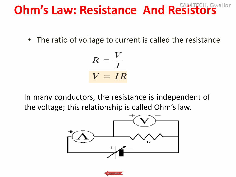
Ohm’s Law: Resistance And Resistors
• The ratio of voltage to current is called the resistance
In many conductors, the resistance is independent ofthe voltage; this relationship is called Ohm’s law.

Kirchhoff’s Current Law (KCL)
• The sum of currents entering any point in a circuit is equal to the sum of currents leaving that point.
• Otherwise, charge would accumulate at the point, reducing or obstructing the conducting path.
• Kirchhoff’s Current Law may also be stated as
IIN = IOUT
In Fig. : Current IC out from point P equals 5A + 3A into P.

Kirchhoff’s Voltage Law (KVL)
• A loop is a closed path.
• This approach uses the algebraic equations for the voltage around the loops of a circuit to determine the branch currents.
• Use the IR drops and KVL to write the loop equations.
• A loop equation specifies the voltages around the
loop.
• Loop Equations
– ΣV = VT means the sum of the IR voltage drops must equal the applied voltage. This is another way of stating Kirchhoff’s Voltage Law.

Phase I - Module No. FC-03

ACTIVE COMPONENTS AND
PASSIVE COMPONENTS
Components are classified as Active components and Passive components.
• Active components have their own gain or directionality. Semiconductor devices (various types of transistors) and vaccum tubes come under active components.
• Passive components do not have gain or directionality. In the perspective of electrical technology, Passive components are known as electrical components or elements. Passive components are capacitors, inductors,resistorsand diodes.
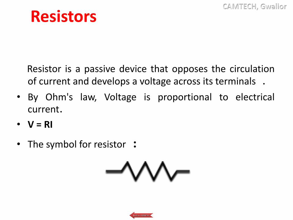
Resistor is a passive device that opposes the circulationof current and develops a voltage across its terminals .
• By Ohm's law, Voltage is proportional to electricalcurrent.
• V = RI
• The symbol for resistor :
Resistors

Resistors
• Resistors can be either fixed or variable in value
• Fixed resistors come in a variety of different shapes, sizes and forms
• Axial lead resistors have the value of resistance printed on them or as a colour code
• Surface mount resistors have a numerical code indicating a value
• All resistors have a tolerance value

Resistors
• Variable resistors are called potentiometers
• There is a fixed value of resistance between two terminals
• The moving part of the potentiometer is called the wiper

Resistors
• Four band resistor colour code
• 1st band provides the first digit of the code
• 2nd band provides the second digit of the code
• 3rd band is the multiplier
• 4th band indicates the tolerance value

Resistors
Resistor colour code calculation-
• The first band red has a value of 2
• The second band purple has a value of 7
• The third band has a multiplier of x 10
• The last band indicates a tolerance value of +/-5%
• Resistance value is 270Ω +/-5%
2
7
x10
+/-5%


Temperature Coefficient of Resistance (TCR)
• A resistor's Temperature Coefficient ofResistance (TCR) tells how much its valuechanges as its temperature changes. It isusually expressed in ppm/°C (parts per millionper degree Centigrade) units.

Resistance
• When an electric current flows through a circuit, there will be some resistance that opposes it. (similar to friction)
• It can be measured by dividing voltage by the current.
R = V
I
R = ResistanceV = VoltageI = Current

Resistance
• Good conductors of electricity have low resistance. (Eg. Metal objects)
– Electricity is able to flow through them very easily
• Poor conductors of electricity have high resistance. (Eg. Wood, cloth)
– Electricity is not able to flow through them easily
• The SI unit for resistance is ohm ()
• Different electrical components have different resistance
• For example, nichrome wires have a higher resistance than
copper wires.
Resistance

Example
• An electric rice cooker operates at 240 V and uses a current of 8 A. What is the resistance of the rice cooker?
Voltage (V) = 240 VCurrent (I) = 8 A
R = V
I
R = 240
8
= 30

Resistors
• An electrical component that is specially made to have a certain resistance is called a resistor.
• They can be connected in a circuit to resist the current flow.

Fixed Resistors and Variable Resistors
• Fixed resistors have only one resistance value
• Variable resistors can be adjusted to change the resistance.
fixed resistor symbol variable resistor symbol
Variable resistors are useful in light dimmers and other electric appliances

Resistors
• Resistors can be connected in series or parallel
single resistor
extra resistor in
series results in
dimmer bulb
extra resistor in
parallel results
in brighter bulb

Resistors in Series
2 3
The total resistance for this circuit is:
2 + 3 = 5
• When resistors are connected in series, the resistance will add up and increase.
• R = R1 + R2 + R3…

• When resistors are connected in parallel, the resistance will decrease
• This is because they will provide alternate routes for the current to flow.
Resistors in Parallel
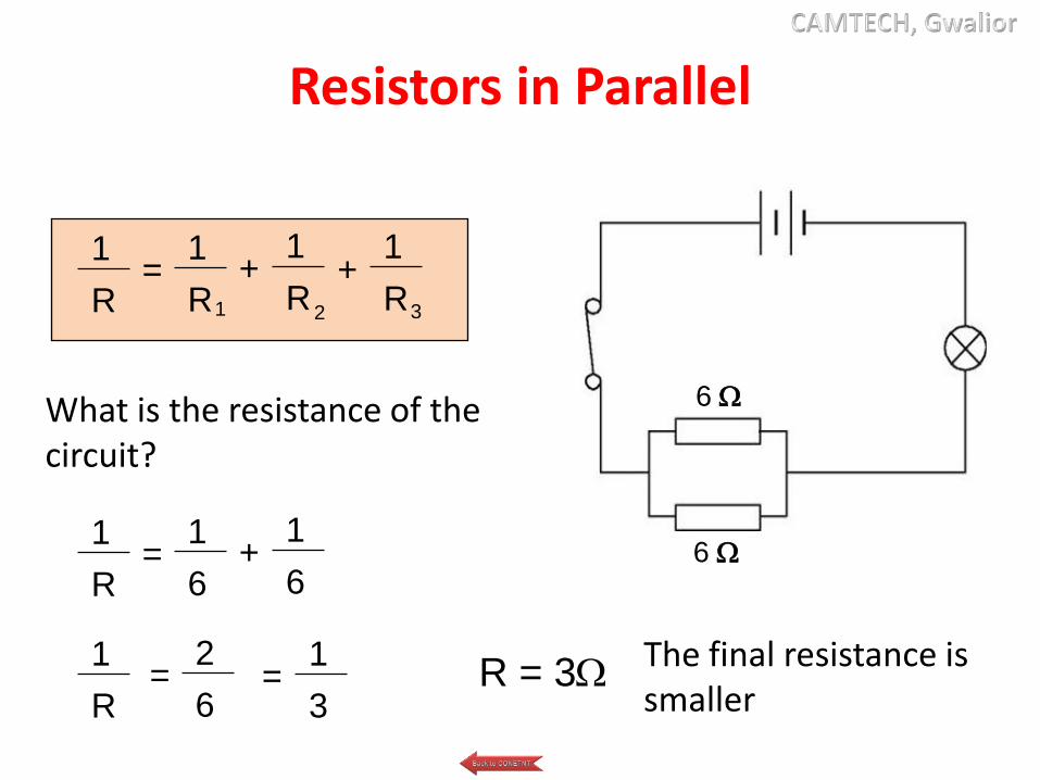
Resistors in Parallel
6
6
1
R=
1
R
1
R
1
R+ +
1 2 3
What is the resistance of the circuit?
1
R=
1
6
1
6+
1
R=
2
6
1
3= R = 3
The final resistance is smaller

Capacitors
• A basic capacitor has two parallel plates separated by an insulating material
• A capacitor stores an electrical charge between the two plates
• The unit of capacitance is Farads (F)
• Capacitance values are normally smaller, such as µF, nF or pF

Capacitors
• Basic capacitor construction
Dielectric material
Plate 1
Plate 2The dielectric material is an insulator therefore no current flows through the capacitor

Capacitors
Storing a charge between the plates -
• Electrons on the left plate are attracted toward the positive terminal of the voltage source
• This leaves an excess of positively charged holes
• The electrons are pushed toward the right plate
• Excess electrons leave a negative charge
+ -
+_
+ _

Capacitors
Types of capacitors –
• The dielectric material determines the type of capacitor
• Common types of capacitors are:
– Mica
– Ceramic
– Plastic film

Capacitors
• Some capacitors are polarised, they can only be connected one way around
• Electrolytic capacitors are polarised

Capacitors
• Variable capacitors are used in communication equipment, radios, televisions and VCRs
• They can be adjusted by consumers by tuning controls
• Trimmers are internal adjusted capacitors that a consumer cannot adjust

Capacitors
• These variable capacitors would be difficult to squeeze into your mobile phone and iPod
• Current technology uses semi-conductor variable capacitors called varactors (varicaps)
Inductor
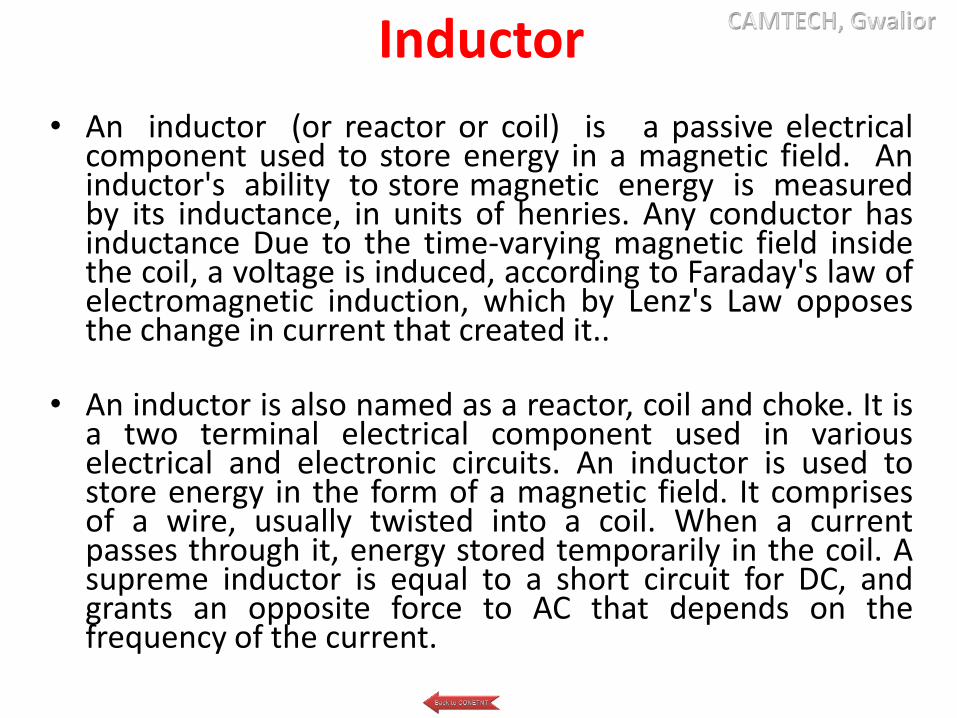
• An inductor (or reactor or coil) is a passive electricalcomponent used to store energy in a magnetic field. Aninductor's ability to store magnetic energy is measuredby its inductance, in units of henries. Any conductor hasinductance Due to the time-varying magnetic field insidethe coil, a voltage is induced, according to Faraday's law ofelectromagnetic induction, which by Lenz's Law opposesthe change in current that created it..
• An inductor is also named as a reactor, coil and choke. It isa two terminal electrical component used in variouselectrical and electronic circuits. An inductor is used tostore energy in the form of a magnetic field. It comprisesof a wire, usually twisted into a coil. When a currentpasses through it, energy stored temporarily in the coil. Asupreme inductor is equal to a short circuit for DC, andgrants an opposite force to AC that depends on thefrequency of the current.

• A diverse electronic component used in a wide range ofapplications requires various types of inductors. Theseare of different shapes, sizes including the wire woundand multilayer inductors. Different types of inductorsinclude high-frequency inductors, power supply lineinductors or power inductors and inductors for generalcircuits. Differentiation of the inductors is based on thetype of winding as well as the core used.
Types of Inductors
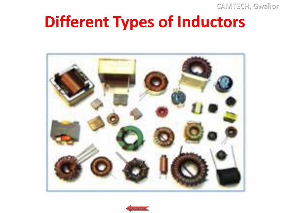
Different Types of Inductors

Air Core Inductors
Ferro Magnetic or Iron Core
Inductors
Ferrite Core Inductors
Toroidal Core Inductors
Bobbin based Inductors
Multi Layer Inductors
Thin Film Inductors
Different Types of Inductors
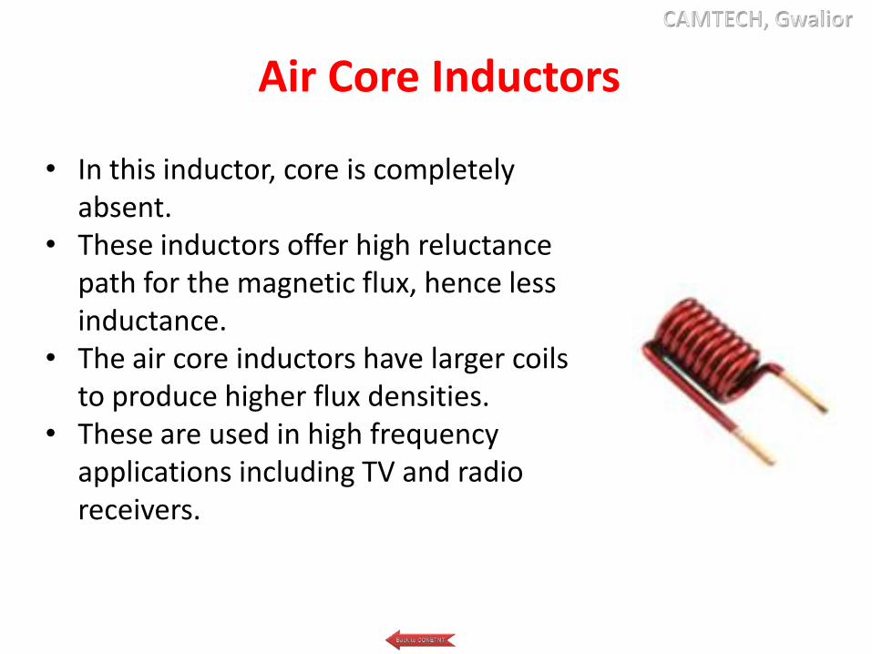
Air Core Inductors
• In this inductor, core is completely absent.
• These inductors offer high reluctance path for the magnetic flux, hence less inductance.
• The air core inductors have larger coils to produce higher flux densities.
• These are used in high frequency applications including TV and radio receivers.

Ferro Magnetic or Iron Core Inductors
• Due to their higher magnetic permeability these have high inductance property.
• These are high power inductors but limited in higher frequency capacity due to the hysteresis and eddy current losses.
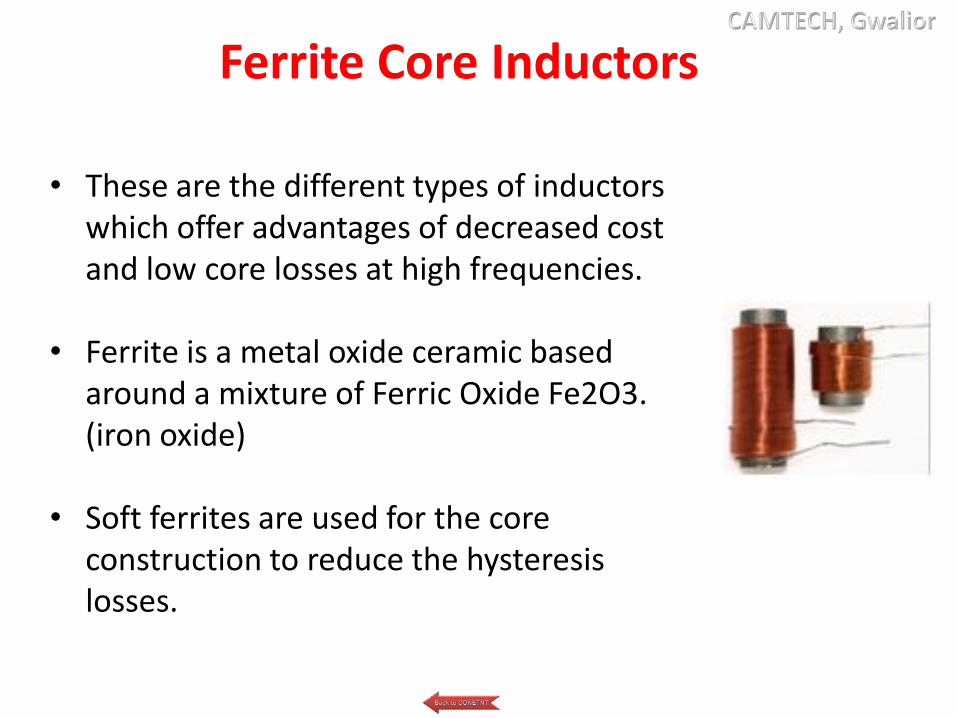
Ferrite Core Inductors
• These are the different types of inductors which offer advantages of decreased cost and low core losses at high frequencies.
• Ferrite is a metal oxide ceramic based around a mixture of Ferric Oxide Fe2O3. (iron oxide)
• Soft ferrites are used for the core construction to reduce the hysteresis losses.

Toroidal Core Inductors
• In these inductors, a coil is wounded on a toroid circular former.
• Flux leakage is very low in this type of inductor.
• Special winding machines are required to design this type of inductor.
• Sometimes ferrite core is also used to decrease the losses in this design.

Bobbin based Inductors
• In this type of Inductor coil is wounded on the bobbin.
• Bobbin wound inductor designs vary widely in terms of power rating, voltage and current levels, operating frequency, etc.
• These are mostly used in switch mode power supplies and power conversion applications.
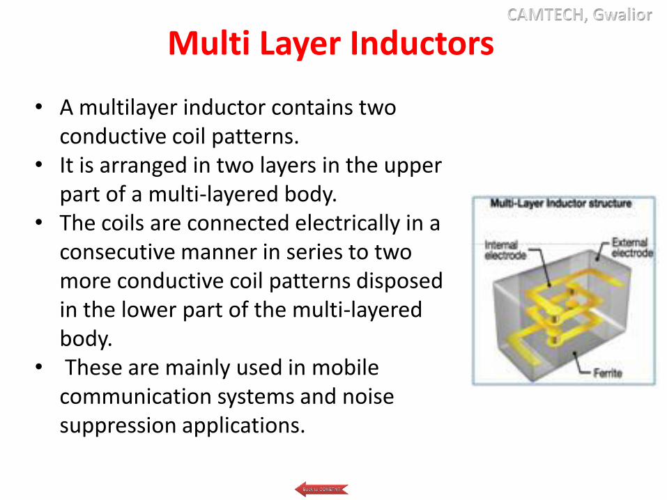
Multi Layer Inductors
• A multilayer inductor contains two conductive coil patterns.
• It is arranged in two layers in the upper part of a multi-layered body.
• The coils are connected electrically in a consecutive manner in series to two more conductive coil patterns disposed in the lower part of the multi-layered body.
• These are mainly used in mobile communication systems and noise suppression applications.

Thin Film Inductors
• These are completely different from the conventional chip-type inductors wound with copper wire.
• In this type of inductors , tiny inductors are formed using thin-film processing to create the chip inductor for high-frequency applications, which ranges from about nano Henry.

How Inductor Works ??
• An inductor is often referred to as AC resistor. It resiststhe changes in the current and stores energy in the formof the magnetic field. These are simple in construction,consisting of the coils of copper wire wounded on acore. This core might be magnetic or air.

Semiconductor Physics, Construction and Operating principle
Semiconductor Materials

• A Silcon Atom.• Some materials, such as copper, aluminium and brass
pass electric currents very easily. As they conductelectricity readily, their ability to resist the flow ofcurrent is low. They therefore have very low resistivityand so are classed as conductors.
• Other materials such as plastics or glass have extremelyhigh resistivity so do not conduct electricity. Thesematerials are called insulators.
• Materials that have a resistivity mid-way between theconductors and insulators do conduct current, but verypoorly at normal room temperatures, and so these arecalled semi-conductors.
• How well or poorly any material conducts electricitydepends on the atomic structure of the material.
Semiconductor Materials

• Silicon and Germanium, materials in the semiconductorgroup are widely used in the manufacture of transistorsand diodes, as well as integrated circuits such asmicroprocessors.
• To make such semiconductor materials suitable for use intransistors and diodes the resistivity of the material ismodified in a controlled way by first making very purecrystals of the semiconductor material. These crystalscontain only atoms of one type (for example silicon)arranged in a regular lattice formation. This very purematerial is then "doped" by adding tiny amounts ofimpurity atoms (about 1 impurity atom in every 10million).
Semiconductor Materials

• The idea is that pure semiconductors conduct poorly,because the electrons in their lattice structure are mostlybound very tightly to their atoms, leaving only a fewelectrons free to move, from atom to atom, through thematerial, so forming a very weak electric current. Byadding impurities with different atomic structures eithermore, or in other cases, less free electrons are added.This controls the ability of the semiconductor to passcurrent, by effectively changing the resistivity of thematerial.
Semiconductor Materials

• Some impurities such as Arsenic and Phosphorus addextra free electrons (negative charge carriers) to thematerial. This is called N type semiconductor.
• Other impurities such as Aluminium and Boron can beadded in order to remove free electrons, so that theresulting material has fewer free electrons than before.Each missing electron within the crystal structure iscalled a "hole". As free electrons are negative chargecarriers, these holes in the structure are really positivecharge carriers. Material doped in this way is called Ptype semiconductor.
Semiconductor Materials
• Putting P type and N type materials next to each other ina circuit creates a PN junction, and makes a useful devicethat is called a diode. When a voltage is applied across adiode a current will flow through the diode in onedirection but not the other.
• Making a three-part sandwich (PNP or NPN) and carefullycontrolling the levels of doping in the three layers createsa transistor capable of amplification, as well as manyother useful functions.
Semiconductor Materials

• Transistors, diodes and integrated circuits can all beclassified as semiconductors because they are made fromsemiconductor materials, Silicon and Germanium beingthe most common. Early types of transistors and diodeswere made from Germanium, but Silicon is used today forthe vast majority of devices. Some germanium types arestill used however, because they possess a number ofuseful properties that silicon does not.
• The resistance of a material indicates how well or howbadly the material conducts (allows the movement ofelectrons under the influence of an electric potential orvoltage). The higher the value of resistance, the moredifficult it is to move the electrons. materials with higherresistance will therefore need a higher potential (highervoltage) applied to cause a given amount of current,(movement of electrons).
Silicon and Germanium in Diodes and Transistors

• As temperature rises within the conductor, thevibration of the atomic structure increases, and sothere are more free electrons being shaken loosefrom their orbits. This gives rise to more collisionswith the electrons moving under the influence of theelectric potential, making the flow of electronstowards the positive electrical potential moredifficult. Therefore the resistance of a conductorslightly increases as its temperature rises.
• Heat also causes a vibration within the atomicstructure and this vibration "shakes loose" some ofthe more easily detached electrons allowing them tomigrate randomly from atom to atom.
The Effects of temperature on a conductor
• An insulator has all its electrons tightly bonded tothe nucleus and so it takes very large forces of eitherheat or potential to dislodge them.
• Insulators do not normally pass current. In somecases, for example at high temperatures or with veryhigh voltages applied, some insulating materials willconduct. In these circumstances the insulatingmaterial is said to have "Broken down" and usuallythe structure of the material is permanentlydamaged.
INSULATORS

• In some insulators (glass for example) heating thematerial to a high temperature will vibrate the atomsso violently that it will shake free enough electronsfor conduction to occur. Cooling the material oncemore stops conduction. In most insulators however,conduction in a normally insulating material,whether caused by excessive heat or by excessivevoltage will permanently destroy the material.
• For this reason insulating materials for electricalinsulators, each have a safe working limit quoted bythe manufacturer using the material, for both voltageand temperature.
INSULATORS

• Semiconductors fall between these twogroups. They do not normally pass currenteasily at room temperature, having aresistivity, somewhere between conductorsand insulators. They have properties howeverwhich make them very useful in electronicdevices.
• The difference between the three groups ofmaterials lies in the number of easilydetached electrons within the atomicstructure. The electrons concerned are moreor less loosely held in the outermost electronshells called valence shells and so theseelectrons are called valence electrons.
Semiconductors

• In a semiconductor the bond betweenthe Valence electrons and their nucleus ismuch stronger than in a conductor, so farfewer electrons are free to move when apotential is applied. When current doesflow, the chances of a collision betweenthe electrons moving due to the electricpotential, and randomly movingelectrons due to heat, is much less.
Semiconductors

• Additionally the heating of the material frees electronspreviously held by their atoms and so these electrons arealso free to add to the current flow. Although of coursethe total current flow is much less than in a conductor,the amount by which current flow increases due to heatis proportionally greater. In use therefore, it is importantto keep components made from semiconductormaterials, such as transistors, cool. Otherwise an effectcalled thermal runaway can occur.
• This is when an increase in temperature causes anincrease in current, which in turn causes a furtherincrease in temperature, leading to increasing current. Aprocess that can escalate until the material passes somuch current it is destroyed.
Semiconductors

Phase I - Module No. FC-03

Diode
Diodes
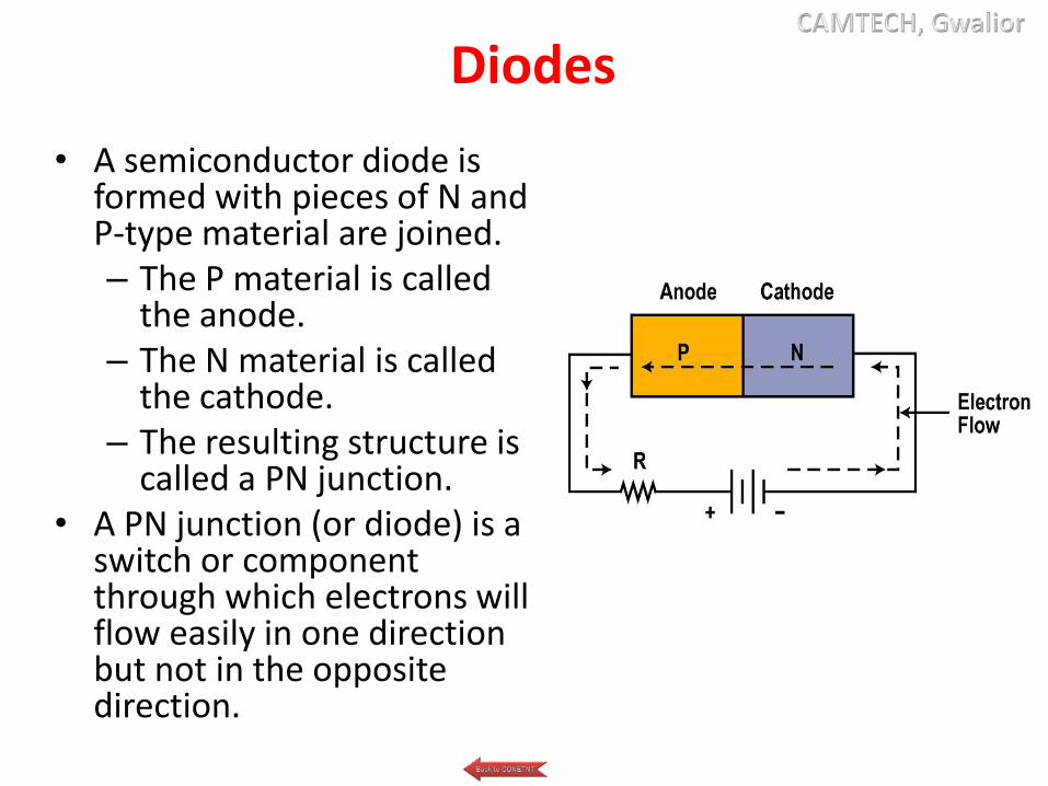
• A semiconductor diode is formed with pieces of N and P-type material are joined. – The P material is called
the anode. – The N material is called
the cathode.– The resulting structure is
called a PN junction.• A PN junction (or diode) is a
switch or component through which electrons will flow easily in one direction but not in the opposite direction.

Biasing a PN Junction
• To get current to flow in PN junction or diode, you have to apply an external voltage called bias.
• With this connection, current only flows freely from cathode across the junction to the anode.
• You’d say the switch is closed when electrons can flow through the diode.
• Note: The current flow may be so high that an external resistance R is usually needed to minimize the current flow to a level a diode can withstand.
• This arrangement is called forward bias.
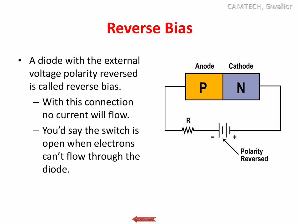
Reverse Bias
• A diode with the external voltage polarity reversed is called reverse bias.
– With this connection no current will flow.
– You’d say the switch is open when electrons can’t flow through the diode.
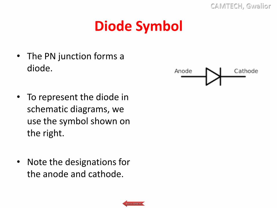
Diode Symbol
• The PN junction forms a diode.
• To represent the diode in schematic diagrams, we use the symbol shown on the right.
• Note the designations for the anode and cathode.

Diode Current Flow
• The direction of current flow (electrons) is shown by the arrow.

A Practical Diode
• A practical diode has two wire leads.
• Note the end with the band circling the body is the cathode end.

Diode Voltage Drop
• Diodes also have a voltage drop while they areconducting. This is called forward voltage drop. It is 0.7volts for silicon diode.
• The forward drop in a germanium diode is 0.3 volts.• Diodes also have a threshold voltage approximately
equal to the forward voltage drop. This is the minimumamount of forward voltage that must be applied to getthe diode to conduct.
• For example if you apply a forward bias of less than abut0.7 volts to a silicon diode, it will not conduct. As soonas the bias voltage rises about 0.7 volts the diode willconduct.

PN Junction Diode characteristics

Zener Diode

Zener Diode
Introduction
The zener diode is a silicon pn junction devices that differsfrom rectifier diodes because it is designed for operation inthe reverse-breakdown region. The breakdown voltage of azener diode is set by carefully controlling the level duringmanufacture. The basic function of zener diode is to maintaina specific voltage across it’s terminals within given limits ofline or load change. Typically it is used for providing a stablereference voltage for use in power supplies and otherequipment.

Example

Construction of Zener
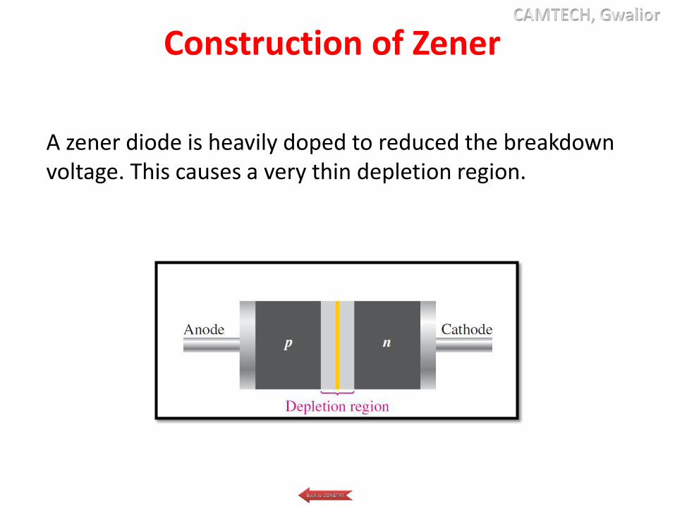
Zener diodes are designed to operate in reverse breakdown. Two types of reverse breakdown in a zenerdiode are avalanche and zener. The avalanche break down occurs in both rectifier and zener diodes at a sufficiently high reverse voltage. Zener breakdown occurs in a zenerdiode at low reverse voltages.
Construction of Zener
A zener diode is heavily doped to reduced the breakdown voltage. This causes a very thin depletion region.

Working of Zener
A zener diode is much like a normal diode. The exception being is that it is placed in the circuit in reverse bias and operates in reverse breakdown. This typical characteristic curve illustrates the operating range for a zener. Note that it’s forward characteristics are just like a normal diode.

DIFFERENCE BETWEEN ZENER AND AVALANCHE BREAKDOWN
Zener Breakdown1.This occurs at junctions which being
heavily doped have narrow depletion
layers
2. This breakdown voltage sets a
very strong electric field across
this narrow layer.
3. Here electric field is very strong
to rupture the covalent bonds
thereby generating electron-hole
pairs. So even a small increase in
reverse voltage is capable of producing
Large number of current carriers.
4. Zener diode exhibits negative temp:
coefficient. Ie. breakdown voltage
decreases as temperature increases.
Avalanche breakdown1. This occurs at junctions which
being lightly doped have wide depletion layers.
2. Here electric field is not strong
enough to produce Zener breakdown.
3. Her minority carriers collide with semi conductor atoms in the depletion region, which breaks the covalent bonds and electron-hole pairs are generated. Newly generated charge carriers are accelerated by the electric field which results in more collision and generates avalanche of charge carriers. This results in avalanche breakdown.
4. Avalanche diodes exhibits positive temp: coefficient. i.e breakdown voltage increases with increase in temperature.
157
LIGHT EMITTING DIODES

158
A light emitting diode (LED) is essentially a PNjunction opto-semiconductor that emits amonochromatic (single color) light when operated ina forward biased direction.
LEDs convert electrical energy into lightenergy. They are frequently used as "pilot" lights inelectronic appliances to indicate whether the circuitis closed or not.
L E D

The most important part of a light emitting diode(LED) is the semi-conductor chip located in the center of thebulb as shown at the right. The chip has two regionsseparated by a junction. The p region is dominated bypositive electric charges, and the n region is dominated bynegative electric charges. The junction acts as a barrier to theflow of electrons between the p and the n regions. Onlywhen sufficient voltage is applied to the semi-conductorchip, can the current flow, and the electrons cross thejunction into the p region.

How Does A LED Work??
• When sufficient voltage is applied tothe chip across the leads of the LED,electrons can move easily in only onedirection across the junction betweenthe p and n regions.
•In the p region there are many morepositive than negative charges.
•When a voltage is applied and thecurrent starts to flow, electrons in the nregion have sufficient energy to moveacross the junction into the p region.

• Each time an electron recombines with a positive charge, electric potential energy is converted into electromagnetic energy.
• For each recombination of a negative and a positive charge, a quantum of electromagnetic energy is emitted in the form of a photon of light with a frequency characteristic of the semi-conductor material (usually a combination of the chemical elements gallium, arsenic and phosphorus)..
How Does A LED Work??

Testing LEDs
• Never connect an LED directly to abattery or power supply! It will bedestroyed almost instantly becausetoo much current will pass throughand burn it out.
• LEDs must have a resistor in seriesto limit the current to a safe value,for quick testing purposes a 1kresistor is suitable for most LEDs ifyour supply voltage is 12V or less.
Remember to connect the LED thecorrect way round!

APPLICATIONS
• Sensor Applications
• Mobile Applications
• Sign Applications
• Automative Uses
• LED Signals
• Illuminations
• Indicators

Sensor Applications
• Medical Instrumentation
• Bar Code Readers
• Color & Money Sensors
• Encoders
• Optical Switches
• Fiber Optic Communication

Mobile Applications
• Mobile Phone
• PDA's
• Digital Cameras
• Lap Tops
• General Backlighting

Signal Appications• Traffic • Rail • Aviation • Tower Lights • Runway Lights • Emergency/Police Vehicle Lighting
LEDs offer enormous benefits over traditional incandescent lamps including:
• Energy savings (up to 85% less power than incandescent)
• Reduction in maintenance costs • Increased visibility in daylight and adverse weather
conditions

Indication
• Household appliances
• VCR/ DVD/ Stereo and other audio and video devices
• Toys/Games
• Instrumentation
• Security Equipment
• Switches

Colours of LEDs (1/3)
LEDs are made fromgallium-based crystals that containone or more additional materialssuch as phosphorous to produce adistinct color. Different LED chiptechnologies emit light in specificregions of the visible lightspectrum and produce differentintensity levels.
Colours of LEDs (1/3)
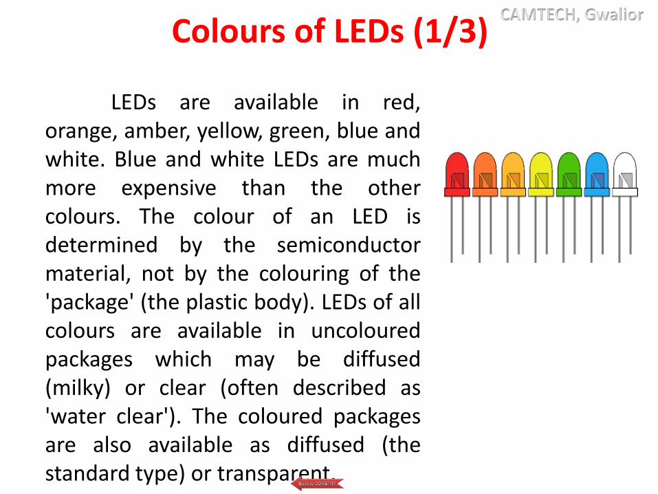
LEDs are available in red,orange, amber, yellow, green, blue andwhite. Blue and white LEDs are muchmore expensive than the othercolours. The colour of an LED isdetermined by the semiconductormaterial, not by the colouring of the'package' (the plastic body). LEDs of allcolours are available in uncolouredpackages which may be diffused(milky) or clear (often described as'water clear'). The coloured packagesare also available as diffused (thestandard type) or transparent.

Colours of LEDs (2/3)
Tri-colour LEDs -The most popular type of tri-colour LED has a red
and a green LED combined in one package with threeleads. They are called tri-colour because mixed red andgreen light appears to be yellow and this is producedwhen both the red and green LEDs are on.
The diagram shows the construction of a tri -colour LED. Note the different lengths of the three leads.The centre lead (k) is the common cathode for both LEDs,the outer leads (a1 and a2) are the anodes to the LEDsallowing each one to be lit separately, or both together togive the third colour.

Colours of LEDs (3/3)
Bi-colour LEDs
A bi-colour LED has two LEDswired in 'inverse parallel' (oneforwards, one backwards) combinedin one package with two leads. Onlyone of the LEDs can be lit at one timeand they are less useful than the tri-colour LEDs described above.

LED Performance
Operating Life
Because LEDs are solid-state devices they are notsubject to catastrophic failure when operated withindesign parameters. LEDs are designed to operateupwards of 100,000 hours at 25°C ambient temperature.Operating life is characterized by the degradation of LEDintensity over time. When the LED degrades to half of itsoriginal intensity after 100,000 hours it is at the end of itsuseful life although the LED will continue to operate asoutput diminishes.

LED Performance
Voltage/Design Current
LEDs are current-driven devices, not voltage driven.Although drive current and light output are directlyrelated, exceeding the maximum current rating willproduce excessive heat within the LED chip due toexcessive power dissipation. The result will be reducedlight output and reduced operating life.
LEDs that are designed to operate at a specificvoltage contain a built-in current-limiting resistor.Additional circuitry may include a protection diode for ACoperation or full-bridge rectifier for bipolar operation. Theoperating current for a particular voltage is designed tomaintain LED reliability over its operating life.

Bargraph 7-segment Starburst Dot matrix
Some Types of LEDs

Transistors

Introduction
A transistor is a device that can be used as either an amplifier or a switch. There are two types of transistor
NPN transistor and PNP transistor.

Transistor Structure
With diodes there is one p-n junction. With bipolar junctiontransistors (BJT), there are three layers and two p-njunctions. Transistors can be either pnp or npn type.

• A transistor is a 3-terminal semiconductor device that is used to amplify or switch.
• By applying an external DC voltage, current will flow from terminal 1 through the device to terminal 3.
• A resistor is used to set the current level.
• A voltage or current applied to terminal 2 is used to control how much current flows from terminals 1 to 3.
• A very small voltage or current variation at terminal 2 can produce a very large current variation between terminals 1 and 3.

• The transistor is connected inseries with a resistor.
• With no (zero) voltage onterminal 2, no current will flowin the transistor. The transistoracts like an open switch. Theoutput voltage is 3 volts asseen through the resistor R.
• If a large enough voltage isapplied to terminal 2, thetransistor will conduct heavilyand act like a very lowresistance between terminals 1and 3. It then acts like a closedswitch. The output voltage isnear zero.
How Transistors Switch

• The circuit is the same as the switch.
• With a small voltage on terminal 2, a large variation in current from terminals 1 to 3 occurs.
• For example, if a sine wave is applied to the input, the current through the transistor will be a sine wave and it will produce a sine wave voltage across the resistor and the transistor.
• Since the current variation in the transistor is very large, the out put voltage is larger than the smaller input voltage.
• The transistor amplifier is said to have gain.
How a Transistor Amplifies
Basic Transistor Operation
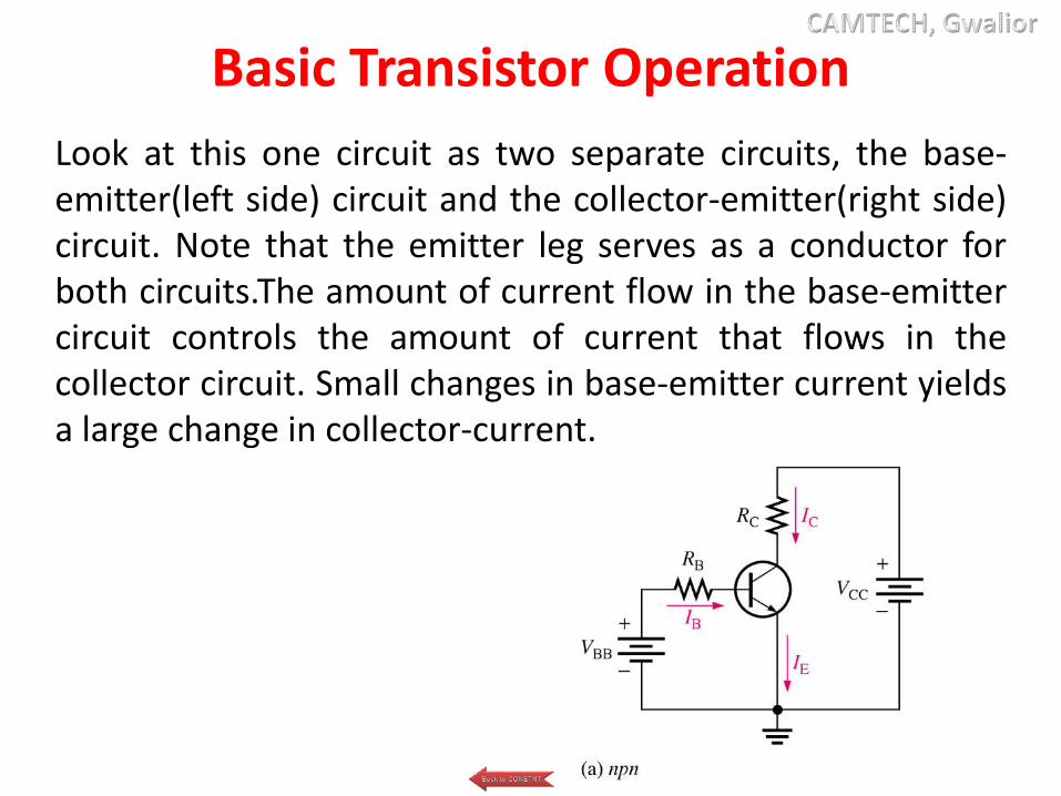
Look at this one circuit as two separate circuits, the base-emitter(left side) circuit and the collector-emitter(right side)circuit. Note that the emitter leg serves as a conductor forboth circuits.The amount of current flow in the base-emittercircuit controls the amount of current that flows in thecollector circuit. Small changes in base-emitter current yieldsa large change in collector-current.

Transistor Characteristics and Parameters
As previouslydiscussed, base-emittercurrent changes yield largechanges in collector-emitter current. The factorof this change is calledbeta ().
= IC / IB
Transistor Bias Circuits

Introduction
For the transistor to properly operate it must be biased.
There are three types of biasing circuit –
1. Voltage-Divider Bias2. Base Bias3. Collector-Feedback Bias
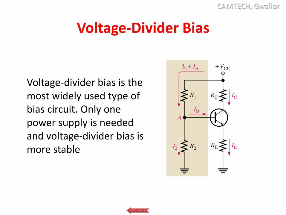
Voltage-Divider Bias
Voltage-divider bias is the most widely used type of bias circuit. Only one power supply is needed and voltage-divider bias is more stable

Base Bias
This type of circuit is very unstable since its changes with temperature and collector current. Base biasing circuits are mainly limited to switching applications.
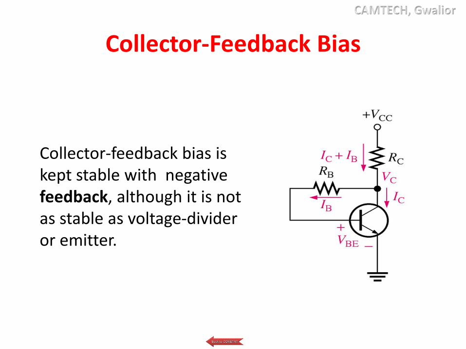
Collector-Feedback Bias
Collector-feedback bias is kept stable with negativefeedback, although it is not as stable as voltage-divider or emitter.

Unijunction Transistor

Unijunction Transistor Symbol and Construction

• The Unijunction Transistor or UJT for short, is anothersolid state three terminal device that can be used in gatepulse, timing circuits and trigger generator applicationsto switch and control either thyristors and triacs for ACpower control type applications.
UJT Symbol and Construction

U J T
• Although the Unijunction Transistor has the name of atransistor, its switching characteristics are very differentfrom those of a conventional bipolar or field effecttransistor as it can not be used to amplify a signal butinstead is used as a ON-OFF switching transistor.
• It consists of n-type silicon bar with an electricalconnection on each end. Leads to these connectionis called base leads. Base 1 and base 2. PN junction isformed between a p-type emitter and bar. Lead iscalled emitter lead E.

• Since emitter is located nearer to B2 more VBB
appears
• Between E & B1.
It will establishes reverse bias on PN junction and emitter current is cut off. Only leakage current will flow.
Working of UJT
No Voltage
V1

• If VEE is applied pn junction will remain in reverse bias till VEE < V1. When VE >V1 pn junction will forward bias .internal voltage drop will decrease.IE increases. The device will turn ON.
• If negative pulse is applied to emitter the pn- junction is reverse biased and emitter current is cut off. The device is turn OFF.
V1
IB
IB
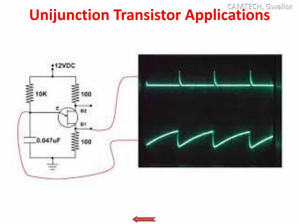
Unijunction Transistor Applications
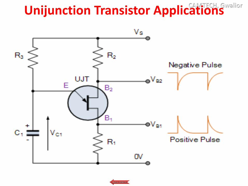
Unijunction Transistor Applications

• When a voltage (Vs) is firstly applied, the unijunctiontransistor is “OFF” and the capacitor C1 is fullydischarged but begins to charge up exponentially throughresistorR3. As the Emitter of the UJT is connected to thecapacitor, when the charging voltage Vc across thecapacitor becomes greater than the diode volt dropvalue, the p-n junction behaves as a normal diode andbecomes forward biased triggering the UJT intoconduction. The unijunction transistor is “ON”.
Unijunction Transistor Applications

• As the ohmic value of resistor R1 is very low, the capacitordischarges rapidly through the UJT and a fast rising voltagepulse appears across R1. Also, because the capacitordischarges more quickly through the UJT than it doescharging up through resistor R3, the discharging time is lessthan the charging time as the capacitor discharges throughthe low resistance UJT.
• When the voltage across the capacitor decreases below theholding point of the p-n junction ( VOFF ), the UJT turns“OFF” and no current flows into the Emitter junction soonce again the capacitor charges up through resistor R3 andthis charging and discharging processbetween VON and VOFF is constantly repeated while there is asupply voltage, Vs applied.
Unijunction Transistor Applications

UJT Oscillator Waveforms

Unijunction Transistor Speed Control

• Using the circuit above, we can control the speed of auniversal series motor (or whichever type of load we want,heaters, lamps, etc) by regulating the current flowingthrough the SCR. To control the motors speed, simplychange the frequency of the sawtooth pulse, which isachieved by varying the value of the potentiometer.
Unijunction Transistor Speed Control

Field Effect Transistors

The JFET
The terminals of a JFET are the source, gate, and drain.
A JFET can be either p channel or n channel.

The JFET
The junction field effect transistor, like a BJT, controls current flow. The difference is that ,The JFET uses voltage to control the current flow. As you will recall the transistor uses current flow through the base-emitter junction to control current. JFETs can be used as an amplifier just like the BJT.
VGG voltage levels control current flow in the VDD, RD circuit.

The JFET
The current is controlled by a field that is developed bythe reverse biased gate-source junction (gate is connectedto both sides). With more VGG (reverse bias) the field (inwhite) grows larger. This field or resistance limits theamount of current flow through RD. With low or no VGG
current flow is at maximum.

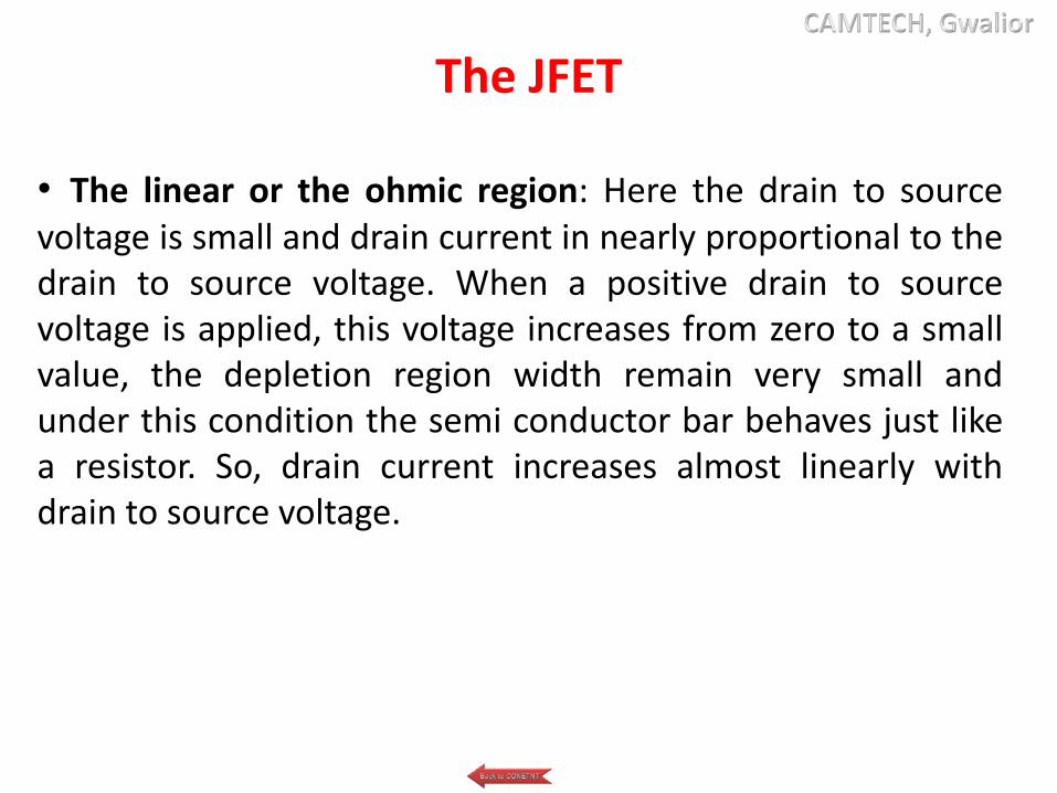
• The linear or the ohmic region: Here the drain to sourcevoltage is small and drain current in nearly proportional to thedrain to source voltage. When a positive drain to sourcevoltage is applied, this voltage increases from zero to a smallvalue, the depletion region width remain very small andunder this condition the semi conductor bar behaves just likea resistor. So, drain current increases almost linearly withdrain to source voltage.
The JFET

• The saturation of the active region: Here the draincurrent is almost constant and it is not dependent on thedrain to source voltage actually. When the drain tosource voltage continuous to increase the channelresistance increases and at some point, the depletionregions meet near the drain to pinch off the channel.Beyond that pinch off voltage, the drain, current attainssaturation.
• The breakdown voltage: Here the drain current increasesrapidly with a small increase of the drain to sourcevoltage. Actually for large value of drain to sourcevoltage, a breakdown of the gate junction takes placewhich results a sharp increase of the drain current.
The JFET

The MOSFET
The IGFET or MOSFET is a voltage controlled fieldeffect transistor that differs from a JFET in that it has a“Metal Oxide” Gate electrode which is electrically insulatedfrom the main semiconductor n-channel or p-channel by avery thin layer of insulating material usually silicon dioxide,commonly known as glass.
This ultra thin insulated metal gate electrode can bethought of as one plate of a capacitor. The isolation of thecontrolling Gate makes the input resistance of theMOSFET extremely high way up in the Mega-ohms ( MΩ )region thereby making it almost infinite.

MOSFETs are three terminal devices witha Gate, Drainand Source and both P-channel (PMOS) and N-channel (NMOS) MOSFETs are available. The main differencethis time is that MOSFETs are available in two basic forms:Depletion Type – the transistor requires the Gate-Sourcevoltage, ( VGS ) to switch the device “OFF”. The depletionmode MOSFET is equivalent to a “Normally Closed” switch.Enhancement Type – the transistor requires a Gate-Sourcevoltage, ( VGS ) to switch the device “ON”. The enhancementmode MOSFET is equivalent to a “Normally Open” switch.
The MOSFET

The symbols and basic construction

The line between the drain and source connectionsrepresents the semi conductive channel. If this is a solidunbroken line then this represents a “Depletion”(normally-ON) type MOSFET as drain current can flowwith zero gate potential. If the channel line is showndotted or broken it is an “Enhancement” (normally-OFF)type MOSFET as zero drain current flows with zero gatepotential. The direction of the arrow indicates whetherthe conductive channel is a p-type or an n-typesemiconductor device.
The MOSFET

The MOSFET
The D-MOSFET can be operated in depletion
or enhancement modes. To be operated in depletion mode, the
gate is made more negative effectively
narrowing the channel or depleting the
channel of electrons.

The MOSFET
To be operated in the enhancement mode the
gate is made more positive, attracting more
electrons into the channel for better
current flow. Remember we are using n channel MOSFETs for discussion purposes. For p channel
MOSFETs, polarities would change.

The MOSFET
The E-MOSFET or enhancement MOSFET can
operate in only the enhancement mode. With a positive voltage on the
gate the p substrate is made more conductive.

Silicon controlled rectifier

SCR
• Most important type of power semiconductordevice.
• Have the highest power handling capability.They have a rating of 5000V / 6000A withswitching frequencies ranging from 1KHz to20KHz.

• Used as a latching switch that can be turnedon by the control terminal but cannot beturned off by the gate.
SCR
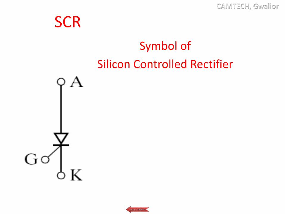
SCR
Symbol of
Silicon Controlled Rectifier

Structure
Gate Cathode
J3
J2
J1
Anode
10 cm17 -3
10 -5 x 10 cm13 14 -3
10 cm17 -3
10 cm19 -3
10 cm19 -3
10 cm19 -3
n+
n+
p-
n–
p
p+
10 m
30-100 m
50-1000 m
30-50 m

Structure

Working of SCR
• The SCR is a four-layer, three-junction and a three-terminal device. The end P-region is the anode, theend N-region is the cathode and the inner P-region isthe gate.
• The anode to cathode is connected in series with theload circuit. Essentially the device is a switch.
• Ideally it remains off (voltage blocking state), orappears to have an infinite impedance until both theanode and gate terminals have suitable positivevoltages with respect to the cathode terminal.

• The SCR then switches on and current flows and continues toconduct without further gate signals.
• Ideally the SCR has zero impedance in conduction state. Forswitching off or reverting to the blocking state, there must beno gate signal and the anode current must be reduced to zero.Current can flow only in one direction.
• SCR can be switched off by applying negative voltage to theanode (reverse mode), the SCR be switched off.
Working of SCR

Equivalent circuit of SCR

Equivalent circuit of SCR
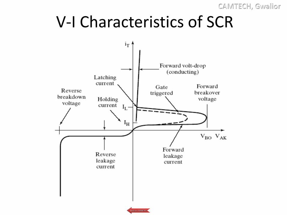
V-I Characteristics of SCR

Effects of gate current

Turn-on Characteristics
on d rt t t

Turn-off Characteristics
Anode currentbegins todecrease
tCtq
t
t
Commutationdidt
Recovery Recombination
t1 t2 t3 t4 t5
trr tgr
tq
tc
VAK
IA
tq=device off time
tc=circuit off time

Methods of Thyristor Turn-on
• Thermal Turn-on.
• Light.
• High Voltage.
• Gate Current.
• dv/dt.

Application of SCR

R-Triggering
LOAD
vO
a b
i R1
R2
D
R Vg
VT
v =V sin tS m
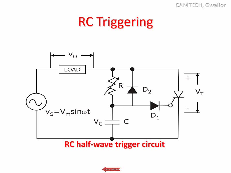
RC Triggering
RC half-wave trigger circuit
LOAD
vO
R
C
VT
v =V sin tS m
D2
VC
+
-D1

Insulated Gate Bipolar Transistor

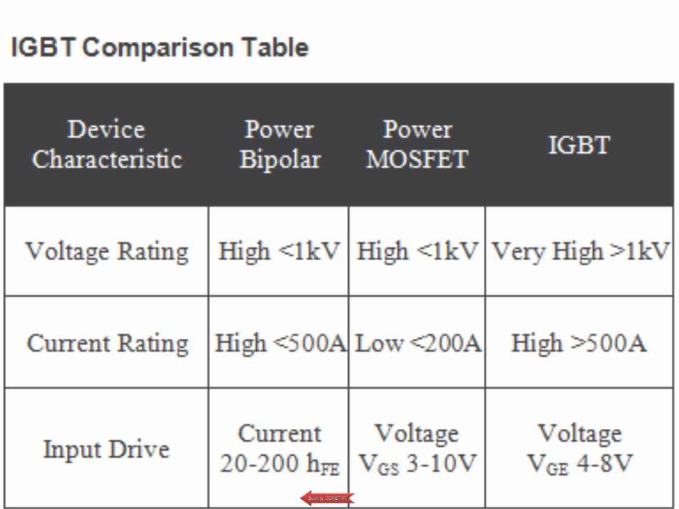
• The Insulated Gate Bipolar Transistoral so calledan IGBT for short, is something of a cross between aconventional Bipolar Junction Transistor, (BJT) anda Metal oxide Field Effect Transistor, (MOSFET) making itideal as a semiconductor switching device.
• The IGBT transistor takes the best parts of these twotypes of transistors, the high input impedance and highswitching speeds of a MOSFET with the low saturationvoltage of a bipolar transistor, and combines themtogether to produce another type of transistor switchingdevice that is capable of handling large collector-emittercurrents with virtually zero gate current drive.
Insulated Gate Bipolar Transistor

• The Insulated Gate Bipolar Transistor, (IGBT) uses theinsulated gate (hence the first part of its name) technology ofthe MOSFET with the output performance characteristics of aconventional bipolar transistor, (hence the second part of itsname). The result of this hybrid combination is that the “IGBTTransistor” has the output switching and conductioncharacteristics of a bipolar transistor but is voltage-controlledlike a MOSFET.
• IGBTs are mainly used in power electronics applications, suchas inverters, converters and power supplies, were thedemands of the solid state switching device are not fully metby power bipolars and power MOSFETs. High-current andhigh-voltage bipolars are available, but their switching speedsare slow, while power MOSFETs may have higher switchingspeeds, but high-voltage and high-current devices areexpensive and hard to achieve.
Insulated Gate Bipolar Transistor

• The advantage gained by the insulated gate bipolartransistor device over a BJT or MOSFET is that it offersgreater power gain than the standard bipolar typetransistor combined with the higher voltage operationand lower input losses of the MOSFET.
• Device that combines an insulated gate N-channel MOSFET input with a PNP bipolar transistor output connected in a type of Darlington configuration. As a result the terminals are labeled as: Collector, Emitter and Gate. Two of its terminals (C-E) are associated with the conductance path which passes current, while its third terminal (G) controls the device.
Insulated Gate Bipolar Transistor

• The Insulated Gate Bipolar Transistor can be used in smallsignal amplifier circuits in much the same way as the BJT orMOSFET type transistors. But as the IGBT combines the lowconduction loss of a BJT with the high switching speed of apower MOSFET an optimal solid state switch exists which isideal for use in power electronics applications.
• Also, the IGBT has a much lower “on-state”resistance, RON than an equivalent MOSFET. This meansthat the I2R drop across the bipolar output structure for agiven switching current is much lower. The forwardblocking operation of the IGBT transistor is identical to apower MOSFET
Insulated Gate Bipolar Transistor

• When used as static controlled switch, the insulated gatebipolar transistor has voltage and current ratings similarto that of the bipolar transistor. However, the presence ofan isolated gate in an IGBT makes it a lot simpler to drivethan the BJT as much less drive power is needed.
• An insulated gate bipolar transistor is simply turned “ON”or “OFF” by activating and deactivating its Gate terminal.Applying a positive input voltage signal across the Gateand the Emitter will keep the device in its “ON” state,while making the input gate signal zero or slightlynegative will cause it to turn “OFF” in much the sameway as a bipolar transistor or eMOSFET. Anotheradvantage of the IGBT is that it has a much lower on-state channel resistance than a standard MOSFET.
Insulated Gate Bipolar Transistor
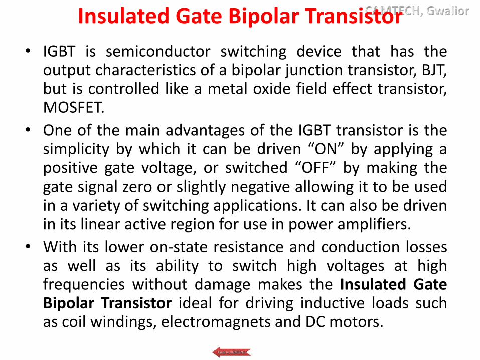
• IGBT is semiconductor switching device that has theoutput characteristics of a bipolar junction transistor, BJT,but is controlled like a metal oxide field effect transistor,MOSFET.
• One of the main advantages of the IGBT transistor is thesimplicity by which it can be driven “ON” by applying apositive gate voltage, or switched “OFF” by making thegate signal zero or slightly negative allowing it to be usedin a variety of switching applications. It can also be drivenin its linear active region for use in power amplifiers.
• With its lower on-state resistance and conduction lossesas well as its ability to switch high voltages at highfrequencies without damage makes the Insulated GateBipolar Transistor ideal for driving inductive loads suchas coil windings, electromagnets and DC motors.
Insulated Gate Bipolar Transistor
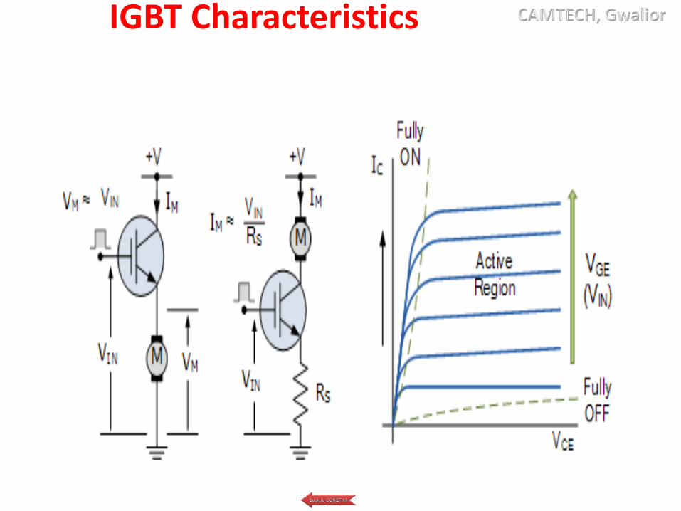
IGBT Characteristics
• Because the IGBT is a voltage-controlled device, it onlyrequires a small voltage on the Gate to maintainconduction through the device unlike BJT’s which requirethat the Base current is continuously supplied in asufficient enough quantity to maintain saturation.
• Also the IGBT is a unidirectional device, meaning it canonly switch current in the “forward direction”, that isfrom Collector to Emitter unlike MOSFET’s which have bi-directional current switching capabilities (controlled inthe forward direction and uncontrolled in the reversedirection).
IGBT Characteristics

• The principal of operation and Gate drive circuits for theinsulated gate bipolar transistor are very similar to that of theN-channel power MOSFET. The basic difference is that theresistance offered by the main conducting channel whencurrent flows through the device in its “ON” state is verymuch smaller in the IGBT. Because of this, the current ratingsare much higher when compared with an equivalent powerMOSFET.
• The main advantages of using the Insulated Gate BipolarTransistor over other types of transistor devices are its highvoltage capability, low ON-resistance, ease of drive, relativelyfast switching speeds and combined with zero gate drivecurrent makes it a good choice for moderate speed, highvoltage applications such as in pulse-width modulated (PWM),variable speed control, switch-mode power supplies or solarpowered DC-AC inverter and frequency converter applicationsoperating in the hundreds of kilohertz range.
IGBT Characteristics

GTO
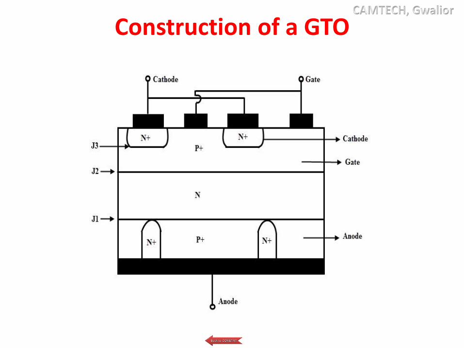
Introduction• Although the thyristor is extensively used in high power
applications, it always suffered from being a semi-controlled device. Even though it could be switched ONby applying a gate signal, it has to be turned OFF byinterrupting the main current using a commutationcircuit. In case of DC to DC and DC to AC conversioncircuits, this becomes a serious deficiency with thyristordue to the absence of natural current zero (as in case ofAC circuits). Hence, the development of Gate Turn offThyristor (GTO) addresses the major problem of thethyristor by ensuring the turn OFF mechanism throughthe gate terminal.

Gate Turn-Off Thyristor
• A Gate Turn off Thyristor or GTO is a three terminal, bipolar(current controlled minority carrier) semiconductorswitching device. Similar to conventional thyristor, theterminals are anode, cathode and gate . As the nameindicates, it has gate turn off capability. These are capablenot only to turn ON the main current with a gate drivecircuit, but also to turn it OFF. A small positive gate currenttriggers the GTO into conduction mode and also by anegative pulse on the gate, it is capable of being turned off.

Observe in below figure that the gate has double arrowsThis indicates the bidirectional current flow through thegate terminal.

• The gate current required to turn off the GTO isrelatively high.
• For example, a GTO rated with 4000V and 3000Amay need -750A gate current to switch it off.
• So the typical turn off gain of GTO is low and is in therange of 4 to 5. Due to this large negative current,GTOs are used in low power applications. On theother hand, during the conduction state GTObehaves just like a thyristor with a small ON statevoltage drop.
• The GTO has faster switching speed than thethyristor and has higher voltage and current ratingsthan the power transistors.
Gate Turn-Off Thyristor

• Consider the below structure of GTO, which is almostsimilar to the thyristor. It is also a four layer, threejunction P-N-P-N device like a standard thyristor. In this,the n+ layer at the cathode end is highly doped to obtainhigh emitter efficiency. This result the breakdown voltageof the junction J3 is low which is typically in the range of20 to 40 volts.
• The doping level of the p type gate is highly gradedbecause the doping level should be low to maintain highemitter efficiency, whereas for having a good turn OFFproperties, doping of this region should be high.
Construction of a GTO
• The junction between the P+ anode and N base is calledanode junction. A heavily doped P+ anode region isrequired to obtain the higher efficiency anode junction sothat a good turn ON properties is achieved.
• However, the turn OFF capabilities are affected with suchGTOs. This problem can be solved by introducing heavilydoped N+ layers at regular intervals in P+ anode layer asshown in figure. So this N+ layer makes a direct contactwith N layer at junction J1. This cause the electrons totravel from base N region directly to anode metal contactwithout causing hole injection from P+ anode. This is calledas a anode shorted GTO structure.
• Due to these anode shorts, the reverse blocking capacity ofthe GTO is reduced to the reverse breakdown voltage ofjunction j3 and hence speeds up the turn OFF mechanism.
Construction of a GTO

• The turn ON operation of GTO is similar to aconventional thyristor. When the anode terminal is madepositive with respect to cathode by applying a positivegate current, the hole current injection from gateforward bias the cathode p-base junction. This results inthe emission of electrons from the cathode towards theanode terminal. This induces the hole injection from theanode terminal into the base region. This injection ofholes and electrons continuous till the GTO comes intothe conduction state.
Gate Turn-Off Thyristor Operation Principles
• To turn OFF a conducting GTO, a reverse bias is applied atthe gate by making the gate negative with respect tocathode. A part of the holes from the P base layer isextracted through the gate which suppress the injectionof electrons from the cathode. In response to this, morehole current is extracted through the gate results moresuppression of electrons from the cathode. Eventually,the voltage drop across the p base junction causes toreverse bias the gate cathode junction and hence theGTO is turned OFF.
Gate Turn-Off Thyristor Operation Principles

• Due to the advantages like excellent switchingcharacteristics, no need of commutation circuit,maintenance-free operation, etc makes the GTO usagepredominant over thyristor in many applications. It isused as a main control device in choppers and inverters.Some of these applications are
• AC drives
• DC drives or DC choppers
• AC stabilizing power supplies
• DC circuit breakers
• Induction heating
• And other low power applications
Gate Turn-Off Thyristor Applications

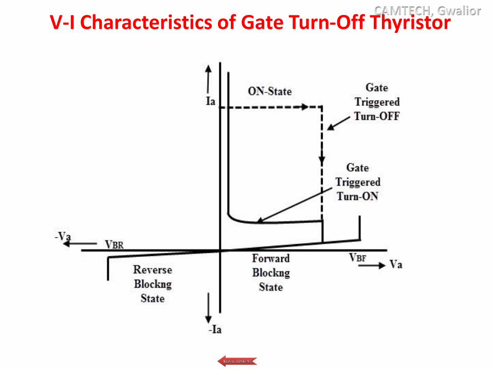
• During the turn ON, GTO is similar to thyristor in itsoperates.So the first quadrant characteristics are similarto the thyristor. When the anode is made positive withrespect to cathode, the device operates in forwardblocking mode. By the application of positive gate signaltriggers the GTO into conduction state. The latchingcurrent and forward leakage currents are considerablyhigher in GTO compared to the thyristor as shown infigure. The gate drive can be removed if the anodecurrent is above the holding current level.
V-I Characteristics of Gate Turn-Off Thyristor

• But it is recommended not to remove the positive gate driveduring conduction and to hold at value more than the maximumcritical gate current. This is because the cathode is subdividedinto small finger elements as discussed above to assist the turnOFF process. This causes the anode current dips below theholding current level transiently, which forces a high anodecurrent at a high rate back into the GTO. This can be potentiallydestructive. Therefore, some manufacturers recommend thecontinuous gate signal during the conduction state.
V-I Characteristics of Gate Turn-Off Thyristor
V-I Characteristics of Gate Turn-Off Thyristor


Phase I - Module No. FC-03

Testing of Resistance

• Switch on your multimeter, and set the dial toresistance mode. Resistance is measured in ohms,indicated by the Ω symbol.
• Most multimeters are not autoranging, meaning youwill need to set the correct range for the resistanceyou expect to measure. If you're not sure, start withthe highest setting.
Testing of Resistance
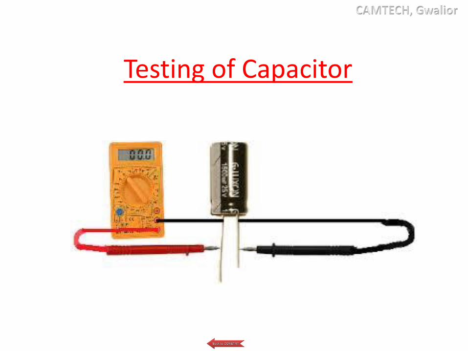
Testing of Capacitor

1. Disconnect the capacitor from its circuit.2. Set your multimeter to its resistance setting. This
setting may be marked with the word “OHM” (Ω), setthe range to 1000 ohm = 1K or higher.
3. Connect the multimeter leads to the capacitorterminals. Again, connect the red lead to the positive(longer) terminal and the black lead to the negative(shorter) terminal.
4. Observe the multimeter reading. Write down theinitial resistance value, if you wish. The value shouldsoon revert to what it was before you connected theleads.
5. Disconnect and reconnect the capacitor severaltimes. You should see the same results as on the firsttest. If you do, the capacitor is good. If, however, theresistance value does not change on any of the tests,the capacitor is dead /defective.
Testing of Capacitor

Capacitor Colour Codes
Types of Capacitor Codes
1. Color coding
2. Number coding

Capacitor Colour Codes
• Generally, the actual values of Capacitance, Voltage orTolerance are marked onto the body of the capacitorsin the form of alphanumeric characters.
• However, when the value of the capacitance is of adecimal value problems arise with the marking of the“Decimal Point” as it could easily not be noticedresulting in a misreading of the actual capacitancevalue. Instead letters such as p (pico) or n (nano) areused in place of the decimal point to identify itsposition and the weight of the number.
Capacitor Colour Codes
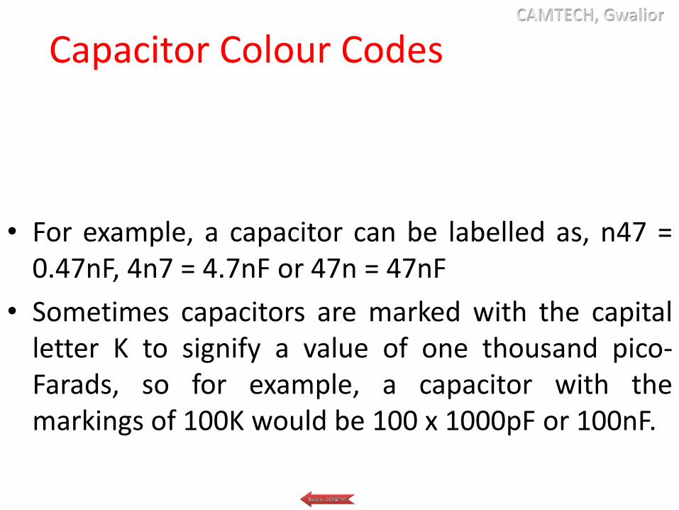
• For example, a capacitor can be labelled as, n47 =0.47nF, 4n7 = 4.7nF or 47n = 47nF
• Sometimes capacitors are marked with the capitalletter K to signify a value of one thousand pico-Farads, so for example, a capacitor with themarkings of 100K would be 100 x 1000pF or 100nF.

Capacitor Colour Codes
• To reduce the confusion regarding letters, numbers anddecimal points, an International colour coding schemewas developed as a simple way of identifying capacitorvalues and tolerances. It consists of coloured bands (inspectral order) known commonly as the CapacitorColour Code system
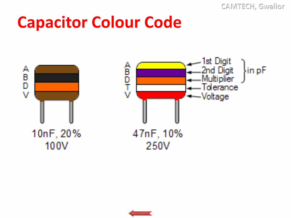
Capacitor Colour Code

Capacitor Colour Code Table

Capacitor Voltage Colour Code Table

Capacitor Voltage Reference
• Type J – Dipped Tantalum Capacitors.
• Type K – Mica Capacitors.
• Type L – Polyester/Polystyrene Capacitors.
• Type M – Electrolytic 4 Band Capacitors.
• Type N – Electrolytic 3 Band Capacitors.

Disc & Ceramic Capacitor

Example

Here we have color coded polyester capacitor. Noting the colors we can formulate the codes and finally we can find out the capacitance value.
Digit 1 Orange 3
Digit 2 Yellow 4
Multiplier White 0.1
Tolerance Red ±0.25pF
There fore Capacitor Value as per equation(1) = 34*0.1 ± 0.25 pF= 3.4 ± 0.25 pF
Example
Number Coding
• The ceramic capacitors have number coding. Theimportant one to be noted is that usually capacitorvalues range is Pico farads (10-12F). Most of them have3 numbers. The 3 numbers are having uniquesignificance. The 1st and 2nd numbers are significantdigits and 3rd one is a multiplier. Mostly the last digitsignifies how many zeroes to be added after the firsttwo digits.

Third Digit Multiplier Value
0 1
1 10
2 100
3 1000
4 10000
5 100000
6 Not Used
7 Not Used
8 0.01
9 0.1
The multiplier table is given below.

Example
• 104K means 10+4 zeroes in pF which is also same as 0.1uF or 100nF.Same procedure in the case of capacitor marked as 103,102 etc.
• The alphabet represents the tolerance.
• Here K means it is having a tolerance of
• +/- 10%

Various letters are used for corresponding tolerances.
Code Tolerance Code Tolerance
A ±0.05pF K ±10%
B ±0.1pF L ±15%
C ±0.25pF M ±20%
D ±0.5pF N ±30%
E ±0.5% P 0 to 100%
F ±1% S -20 to 50%
G ±2% W 0 to 200%
H ±3% X -20 to 40%
J ±5% Z -20 to 80%

Testing of Inductor
• The best test to check whether an inductor is good or not isby testing the inductor's resistance with your multimeterset to the ohmmeter setting.
• By taking the inductor's resistance, we can determinewhether the inductor is good or bad.
• The inductor should read a very low resistance across itsterminals, only a few ohms. If an inductor reads a highresistance, it is defective and should be replaced in thecircuit.
• If an inductor is reading very, very small resistance, lessthan an ohm (very close to 0Ω), this may be a sign that it'sshorted. Functional inductors normally read a few ohms,greater than 1Ω and normally less than 10Ω. This is ahealthy range for an inductance value. Outside this rangeand this is normally a sign the inductor is bad.
Testing of Inductor

Testing of Diode & Zener Diode

• Multimeter set to the ohmmeter setting.• Anode-Cathode Diode Resistance Test• First take the ohmmeter and place the positive probe
on the anode of the diode and the negative probe onthe cathode of the diode .In this setup, the diodeshould read a moderately low resistance, maybe a fewhundred thousands of ohms. For example, you mayread around 450KΩ.
• Cathode-Anode Diode Resistance Test• Now take the ohmmeter and switch the probes around
so that the positive probe of the multimeter is now onthe cathode of the diode and the negative lead on theanode. In this setup now, the diode should read a muchhigher resistance, well over 1MΩ. A typical readingmay, for example, be 2.3MΩ. The multimeter may evenindicate 'OL' for an open circuit, since the resistance isso high.
Testing of Diode & Zener Diode
• Open Diode• If a Diode / Zener diode reads high resistance in both
directions, this is a sign that the diode is open. A diodeshould not measure very high resistance in the forwardbiased direction. The diode should be replaced in thecircuit.
• Shorted Diode• If the Zener diode reads low resistances in both
directions, this is a sign that the diode is shorted. Adiode should not measure low resistance in the reversebiased direction. The diode should be replaced in thecircuit.
Testing of Diode & Zener Diode

Testing of LED

Light emitting diode (LED)is a small component used in almost every electronic device. Led has 2 terminals or legs. The bigger leg is the anode or positive terminal and shorter leg is cathode or negative terminal.
Testing of LED

• Set the digital multimeter on the continuity mode. If you touch the testing leads to each other the multimeter will give a continuous beep sound. The beep sound means that the multimeter is working perfectly.
• Crocodile probes are connected to the LED terminal according to their polarity. Longer leg is connected to the positive supply and shorter to negative (grounded).
1. Power ON the multimeter2. Set the knob on the continuity mode.3. LED will glow indicating that it is in working condition4. If the LED doesn’t glows then check the connections else
the LED is faulty.
Testing of LED

Testing of Transistor
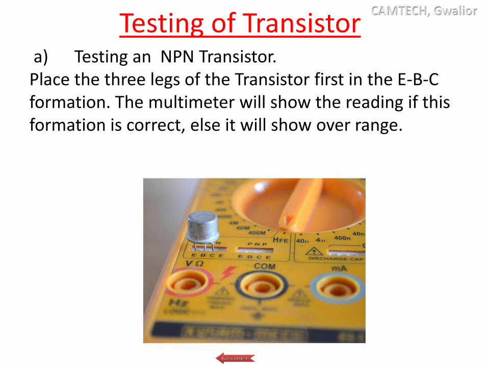
a) Testing an NPN Transistor.Place the three legs of the Transistor first in the E-B-C formation. The multimeter will show the reading if this formation is correct, else it will show over range.
Testing of Transistor

If the previous method doesn’t work, place the threelegs of the Transistor in the B-C-E formation. Ifmultimeter shows reading then it’s correct. The readingis nothing but thr HFE of that transistor.
Testing of Transistor

b) Testing PNP Transistor.Place the three legs of the transistor in the same manner as discussed above.
Testing of Transistor

After placing the transistor in the correct formation, multimeter would show the HFEvalue of the transistor.
Testing of Transistor

• hFE of a transistor is the current gain or amplification factor of a transistor.
• hFE (which is also referred to as β) is the factor by which the base current is amplified which is fed into the transistor.
• A transistor works by feeding a base current into the base of the transistor. The base current is then amplified by hFE to yield its amplified current. The formula is below:
IC= hFEIB=βIB• So if 1mA is fed into the base of a transistor and it has a hFE of
100, the collector current will be 100mA.• Every transistor has its own unique hFE. The hFE is normally
seen to be a constant value, normally around 10 to 500, but it may change slightly with temperature and with changes in collector-to-emitter voltage.
• Check the transistor's datasheet for the hFE value in its specifications.
Testing of Transistor

Testing of FET

• FET are checked by measuring differentresistances by a multimeter. When resistance ischecked between source and drain, it should beof the order of 10 kohms.
• When a JFET is checked as a diode multimetershould indicate low resistance between gate andsource with one polarity and very high resistancebetween gate and source with meter polarityreversed.
• If the meter indicates high resistance with boththe polarities, it means that the gate junction isopen. On the other hand, if meter indicates lowresistance with both polarities, it means that thegate junction is shorted.
Testing of FET

Testing of MOSFET

• While checking MOSFET, the resistancemeasured between gate and drain should beinfinitely high in either polarity. Low resistancemeans faulty device.
Testing of MOSFET

Testing of SCR

• Put the multimeter selector switch in a high resistanceposition. Connect the positive lead of multimeter to theanode of SCR and negative lead to the cathode. Themultimeter will show an open circuit. Now reverse theconnections and the multimeter will again show an opencircuit.
• Then connect the anode and gate terminals of the SCR to thepositive lead of multimeter and cathode to the negative lead.The multimeter will show a low resistance indicating theswitch ON of SCR. Now carefully remove the gate terminalfrom the anode and again the multimeter will show a lowresistance reading indicating the latching condition. Here themultimeter battery supplies the holding current for the SCR. Ifall of the above tests are positive we can assume the SCR tobe working fine.
Testing of SCR