ATOMIC SCALE NANOWIRES -...
54
ATOMIC SCALE NANOWIRES Onur Yavuzçetin Fakultät für Naturwissenschaften Department Physik 1
Transcript of ATOMIC SCALE NANOWIRES -...
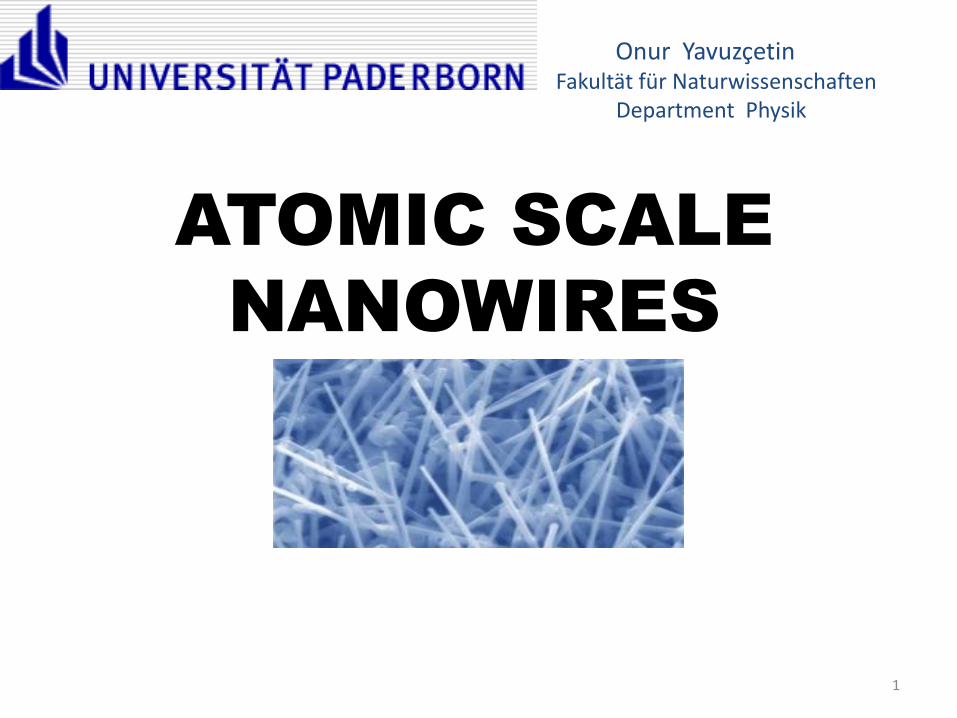
ATOMIC SCALE
NANOWIRES
Onur YavuzçetinFakultät für Naturwissenschaften
Department Physik
1

What is a Nanowire?
• It is a nanostructure with the diameter of the order of a nanometer (10−9 meters) which is extremely small.
• There is no restriction on how wide they can grow, but cannot grow more than a few nanometers in height.
• Have nanometer size in one of the dimension which produces quantum confinement in material and changes its properties.
2
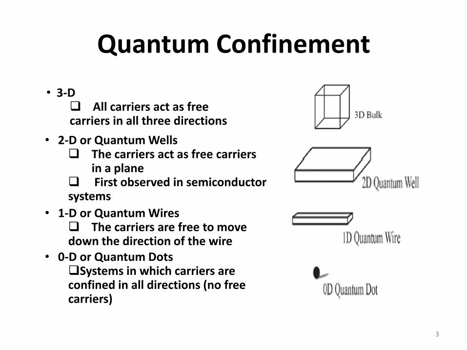
Quantum Confinement
• 2-D or Quantum Wells The carriers act as free carriers
in a plane First observed in semiconductor systems
• 1-D or Quantum Wires The carriers are free to move down the direction of the wire
• 0-D or Quantum DotsSystems in which carriers are confined in all directions (no free carriers)
• 3-D All carriers act as free carriers in all three directions
3

Quantum confinement is responsible for the increase of energy difference between energy states and band gap.
4

1D nanostructures(Quantum Wires)
• 1D nanostructures represent the smallest dimension
structure that can efficiently transport electrical carriers.
• 1D nanostructures can also exhibit such device functions that can be exploited as both wiring and device elements in future architectures for functional nanosystems.
• In this regard, two material classes:
I. (NTs) carbon nanotubes
II. (NWs) nanowires
have shown particular promise
5
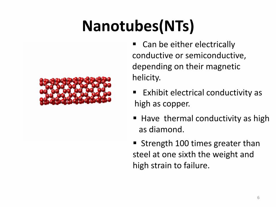
Nanotubes(NTs) Can be either electrically conductive or semiconductive, depending on their magnetic helicity.
Exhibit electrical conductivity ashigh as copper.
Have thermal conductivity as high as diamond.
Strength 100 times greater than steel at one sixth the weight and high strain to failure.
6
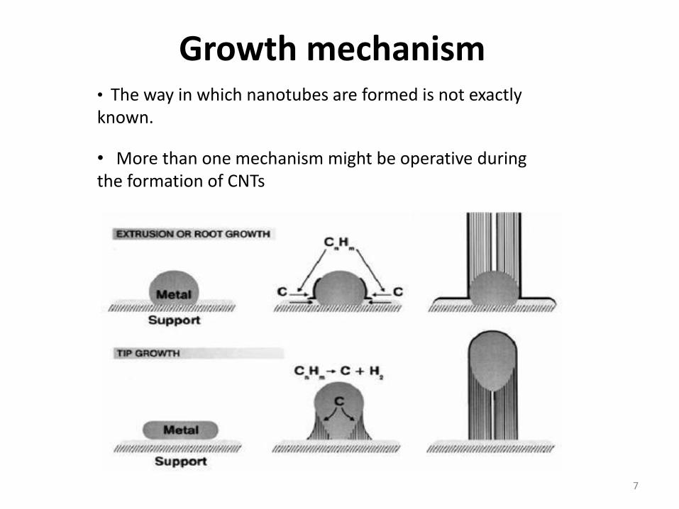
Growth mechanism• The way in which nanotubes are formed is not exactly known.
• More than one mechanism might be operative during the formation of CNTs
7

Synthesis1) Arc discharge
8

Production of SWNTs• a) Inert Gas: Argon with lower diffusion coefficient and
thermal conductivity smaller diameter (1.2nm)
• b)Optical Plasma Control:distance between anode and cathode is increases, anode vaporization increases, The nanotubes diameter ranges from 1.27 to 1.37 nanometer.
• c) Catalyst: By changing metal catalyst, the nanotubeswith a diameter of 0.6 to 1.2nm are produced. Catalysts used are Co and Mo.
• d)Open Air Synthesis with Welding Arc Torch: Steelbased electrode, torch arc aimed at the edge of target and soot is deposited on substrate.
9

Production of MWNTs
• a) Synthesis in Liquid Nitrogen: Arc- discharge generated in liquid nitrogen. Yield is about 70% of reaction product.
• b)Magnetic Field Synthesis :Arc- discharge is controlled by a magnetic field around the arc plasma. Extremely pure graphite rods (purity > 99.999 %) are used as electrodes. Highly pure MWNTs (purity > 95 %) are obtained.
• c) Plasma Rotating Arc Discharge14: The centrifugal force caused by the rotation generates turbulence Plasma volume and the plasma temperature raises. The yield can be increased up to 90% after purification if the rotation speed(5000rpm)
10
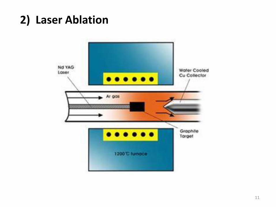
2) Laser Ablation
11
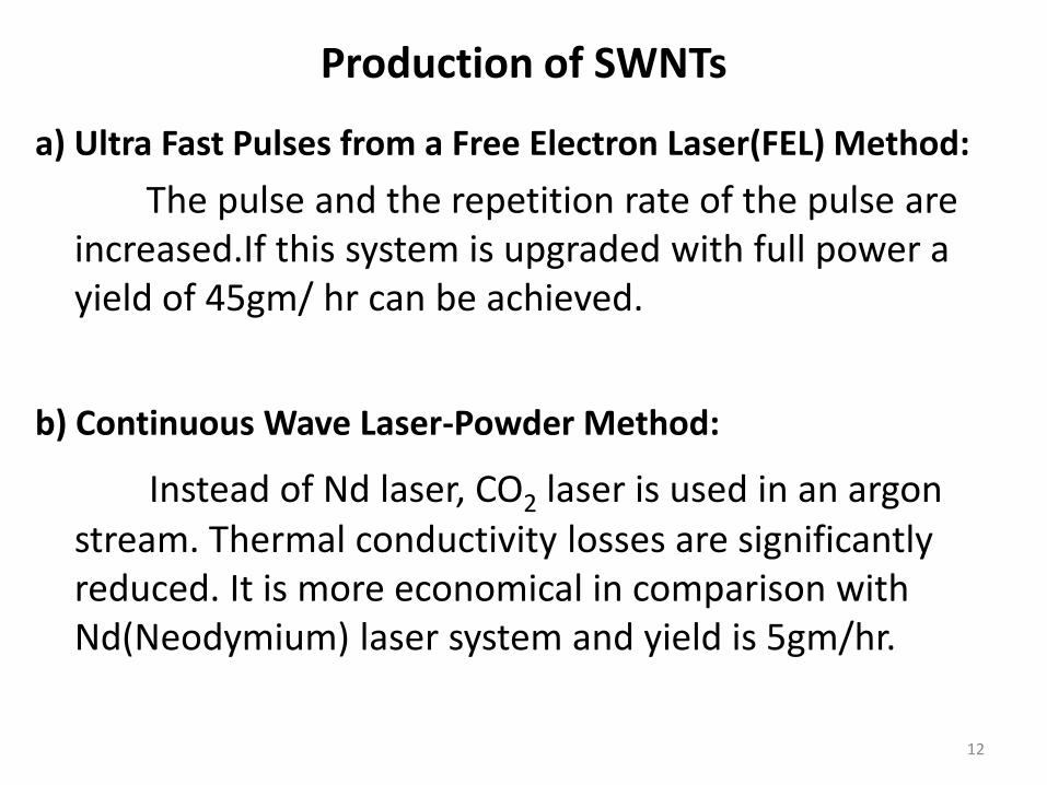
Production of SWNTs
a) Ultra Fast Pulses from a Free Electron Laser(FEL) Method:
The pulse and the repetition rate of the pulse are increased.If this system is upgraded with full power a yield of 45gm/ hr can be achieved.
b) Continuous Wave Laser-Powder Method:
Instead of Nd laser, CO2 laser is used in an argon stream. Thermal conductivity losses are significantly reduced. It is more economical in comparison with Nd(Neodymium) laser system and yield is 5gm/hr.
12

3) Chemical vapour deposition(CVD)
13

Meshes on which the metal catalyst is coated, used in flame synthesis
4) Flame synthesis
14

Types of carbon nanotubes
1) A "chiral" carbon nanotube.
2) A "zig-zag" carbon nanotube
3) An "armchair" carbon nanotube.
15
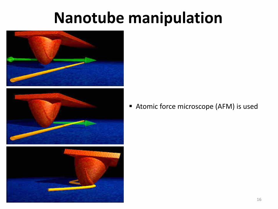
Nanotube manipulation
Atomic force microscope (AFM) is used
16
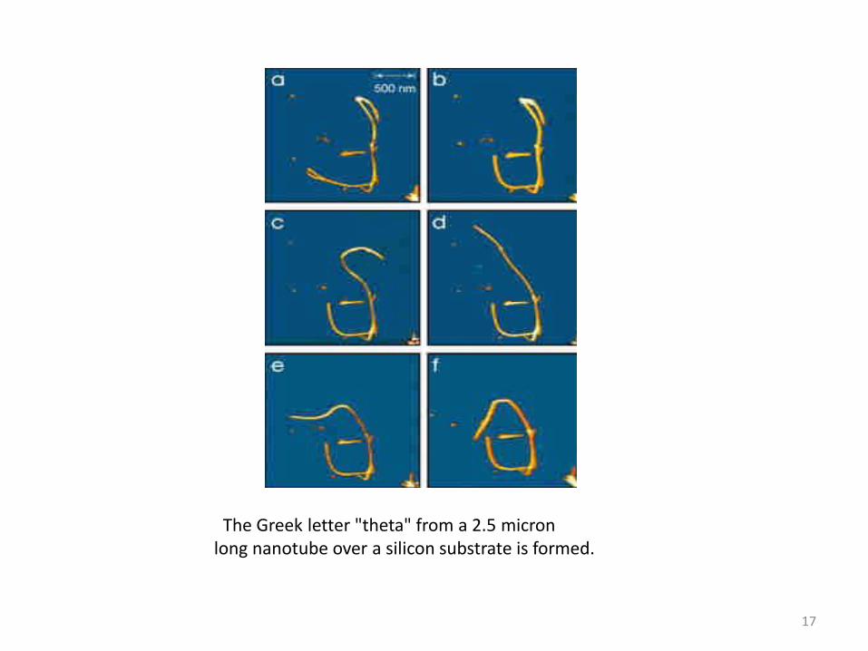
The Greek letter "theta" from a 2.5 micronlong nanotube over a silicon substrate is formed.
17

Applications
• Field-effect transistors
18
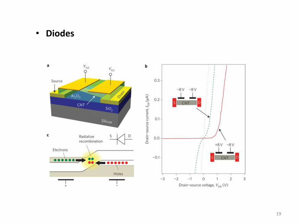
• Diodes
19

• Logic circuits
20
Disadvantages• Difficulties in manipulating individual NTs.
• Difficulties to control whether building blocks are semiconducting or metallic.
• Up to date,device fabrication by NT largely is a random event , posing a significant barrier to achieving highly integrated nanocircuits.
• Stretching a nanotube can either increase or decrease its conductivity--depending on the type of nanotube.
21
Types of Nanowires
• Metallic - Made from Nickel,Platinum or Gold
• Semi-conducting - Comprises of Silicon,Indium phosphide or Gallium Nitride
• Insulating - Silicon Dioxide or Titanium dioxide
• Molecular – Involves repeating organic or inorganic molecular units
22
Synthesis
• Spontaneous growth Evaporation(Dissolution) condensation
Vapor(or solid)-Liquid-Solid growth(VLS or SLS)
Stress induced re-crystallization
• Template-based synthesis Electrochemical deposition
Electrophoretic deposition
Colloid dispersion,melt or solution filling
Conversion with chemical reaction
• Electro-spinning
• Lithography (top-down)
23

Spontaneous Growth
General Idea:
• Anisotropic growth is required.
• Crystal growth proceeds along one direction, where as there is no growth along other direction.
• Uniformly sized nanowires (i.e. the same diameter along the longitudinal direction of a given nanowire)
24
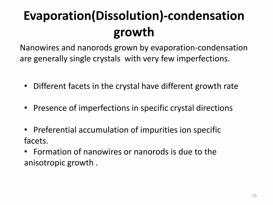
Evaporation(Dissolution)-condensation growth
Nanowires and nanorods grown by evaporation-condensation are generally single crystals with very few imperfections.
• Different facets in the crystal have different growth rate
• Presence of imperfections in specific crystal directions
• Preferential accumulation of impurities ion specific facets. • Formation of nanowires or nanorods is due to the anisotropic growth .
25
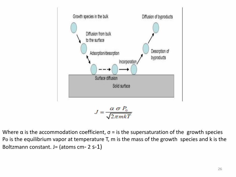
Where α is the accommodation coefficient, σ = is the supersaturation of the growth speciesPo is the equilibrium vapor at temperature T, m is the mass of the growth species and k is the
Boltzmann constant. J= (atoms cm- 2 s-1)
26

At low concentration, growth is diffusion limited and thus increases linear with increasing reactant concentration. At high concentration, surface reaction is the limit step and thus the growth rate becomes independent of reactant concentration.
27
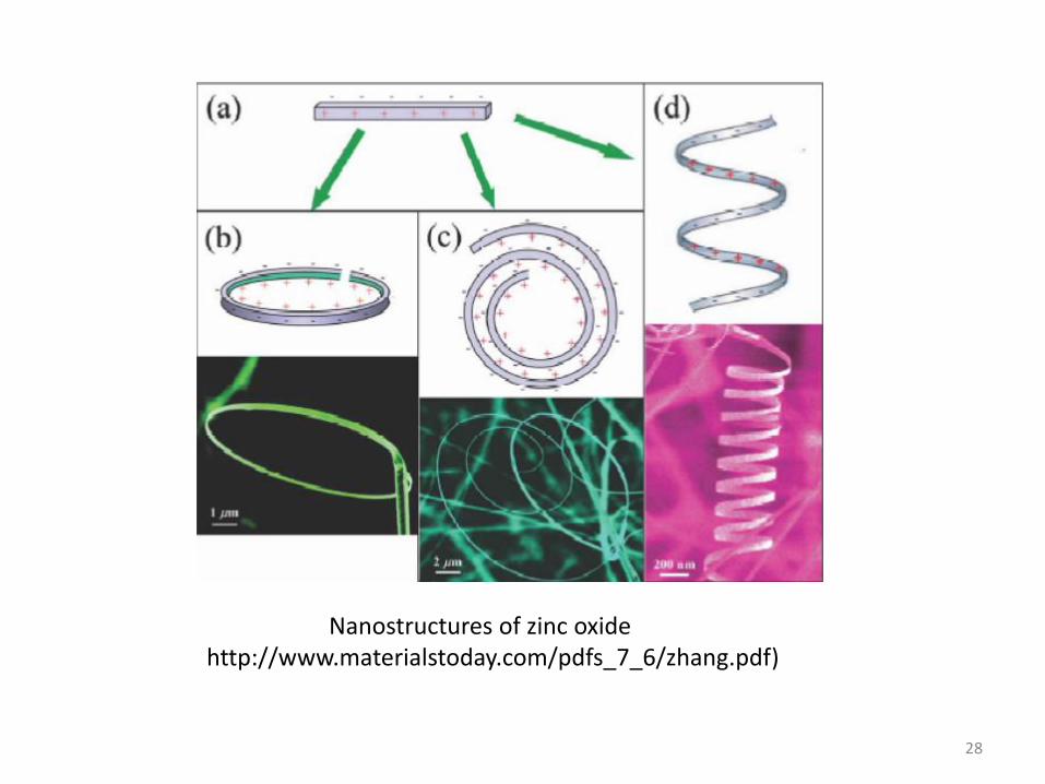
Nanostructures of zinc oxide http://www.materialstoday.com/pdfs_7_6/zhang.pdf)
28
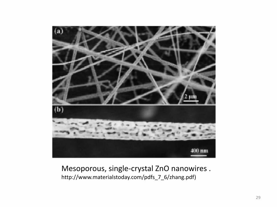
Mesoporous, single-crystal ZnO nanowires .http://www.materialstoday.com/pdfs_7_6/zhang.pdf)
29

Vapor Liquid Solid Growth (VLS)• Catalyst forms a liquid droplet by itself.
• Acts as a trap for growth species.
• The growth species is evaporated first and then diffuses and dissolves into a liquid droplet.
• It precipitates at the interface between the substrate and the liquid.
30
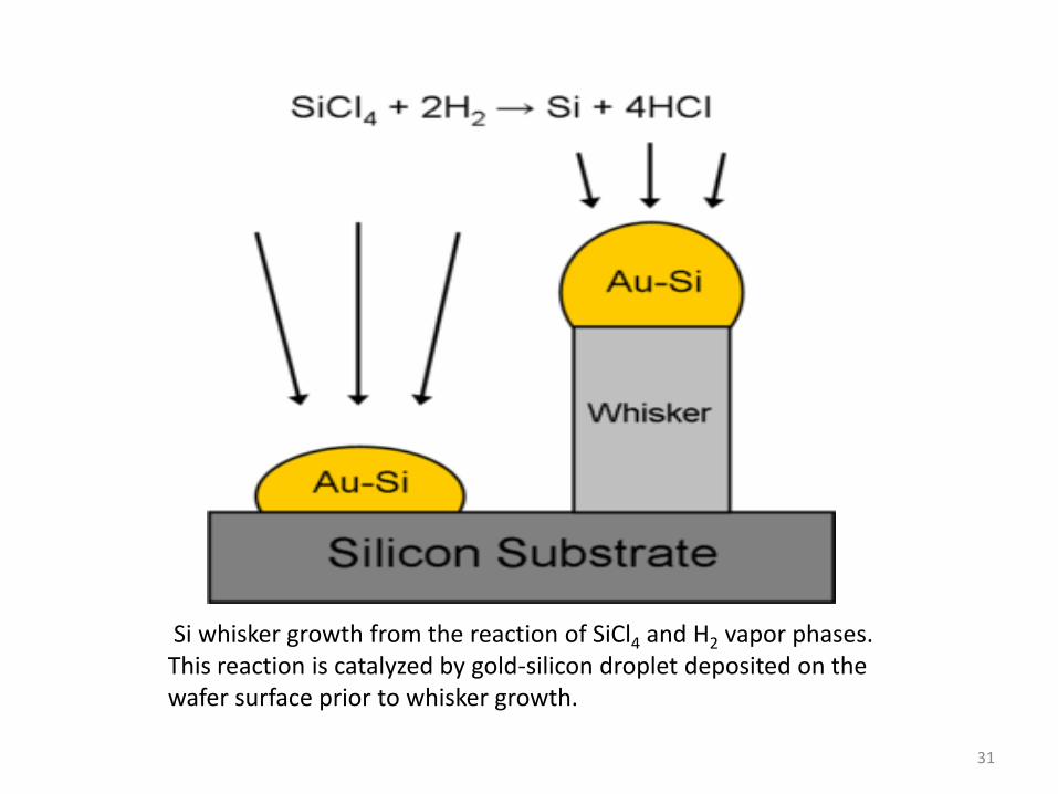
Si whisker growth from the reaction of SiCl4 and H2 vapor phases. This reaction is catalyzed by gold-silicon droplet deposited on the wafer surface prior to whisker growth.
31

A Non-Traditional Vapor-Liquid-Solid Method for Bulk Synthesis of Semiconductor Nanowires
www.cvd.louisville.edu/Publications/recentpublications/proceedings_mrs_fall2001.pdf
32
Stress induced re-crystallization
• Application of pressure on solids at elevated temperatures is
known to result in the growth of whiskers or nanowires with
diameters as small as 50 nm.
• It was demonstrated that the growth rate of tin whiskers
increased proportionally with the applied pressure and could be
four orders of magnitude when a pressure of 7500 psi was applied.
• This technique is not widely explored in the recent studies on the
growth of nanorods and nanowires.
33
Template Base synthesisGeneral Idea:• Use in fabrication of nanorods, nanowires, and
nanotubes of polymers, metals, semiconductors,
and oxides.
• Some porous membrane with nano-size
channels(pores) are used as templates to conduct the
growing of nanowires.
• Pore size ranging from 10 nm to 100 mm can be
achieved.
34
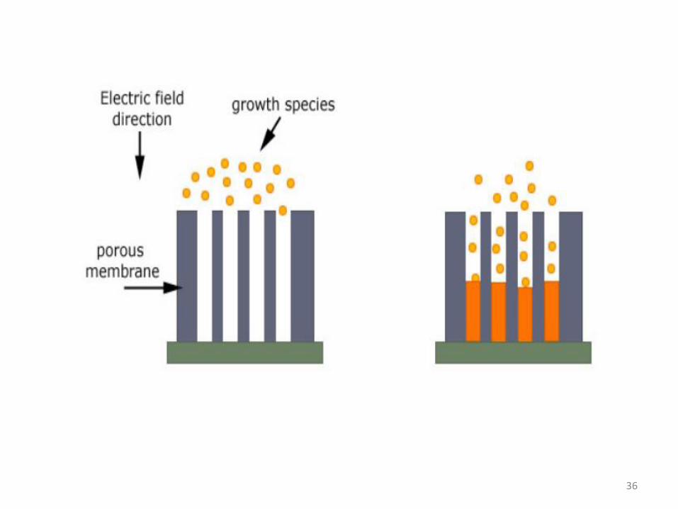
Electrochemical deposition
• This is a self-propagating process
• Only applicable to electrically conductive materials
(metals, alloys, semiconductors, and electrical conductive
Polymers)
• Use prefabricated cylindrical nanopores in a solid material as templates.
• If dissolve away the host solid material, freestanding nanowires are obtained.
35
36
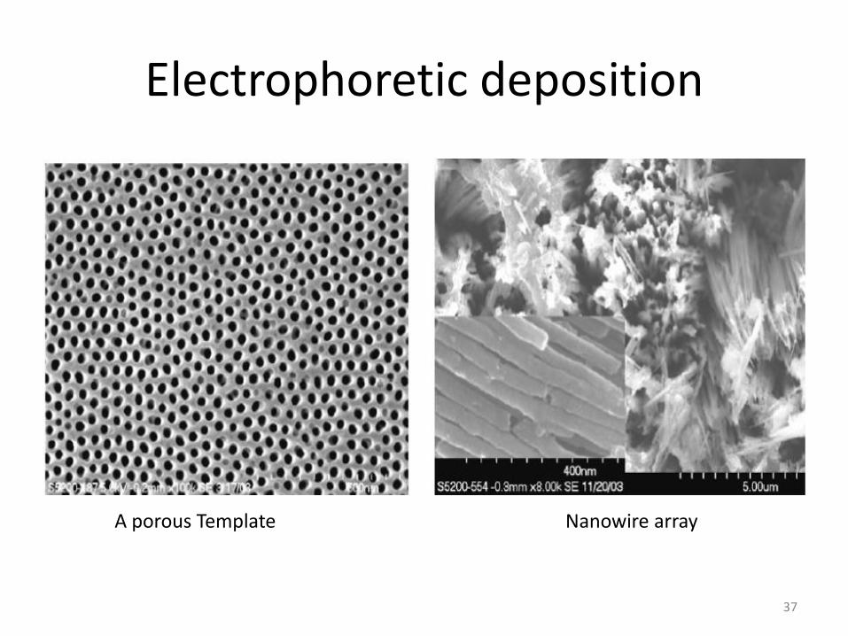
Electrophoretic deposition
A porous Template Nanowire array
37
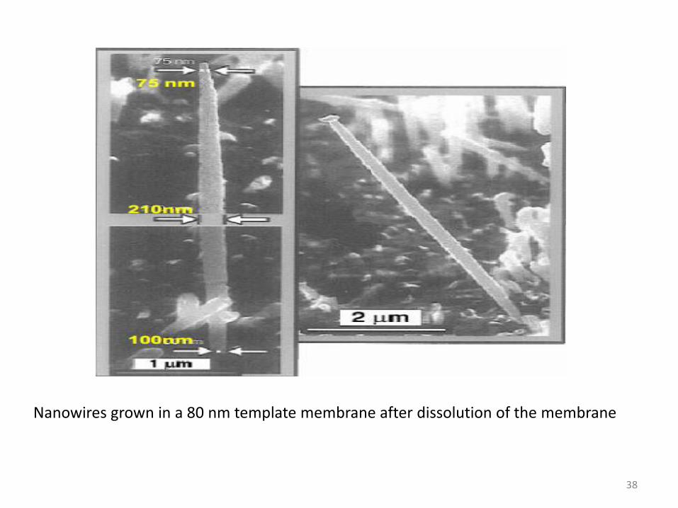
Nanowires grown in a 80 nm template membrane after dissolution of the membrane
38
Advantages
• The ability to create highly conductive nanowires
because electro-deposition relies on electron transfer,
which is the fastest along the highest conductive path.
• Electro-deposited nanowires tend to be dense
continuous and highly crystalline in contrast to other
deposition methods.
• The ability to control the aspect ratio of the metal
nanowires by monitoring the total amount of passed
charge.
39

Electrophoretic Deposition
• Differs from electrochemical deposition in several aspects.
• The deposit doesn’t need to be electrically conductive.
• Particular method for obtaining oxide nanowires like SiO2, TiO2, Bi2O3, etc.
40
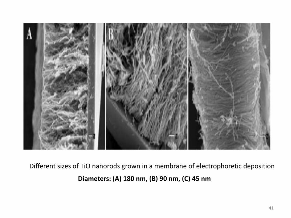
Different sizes of TiO nanorods grown in a membrane of electrophoretic deposition
Diameters: (A) 180 nm, (B) 90 nm, (C) 45 nm
41
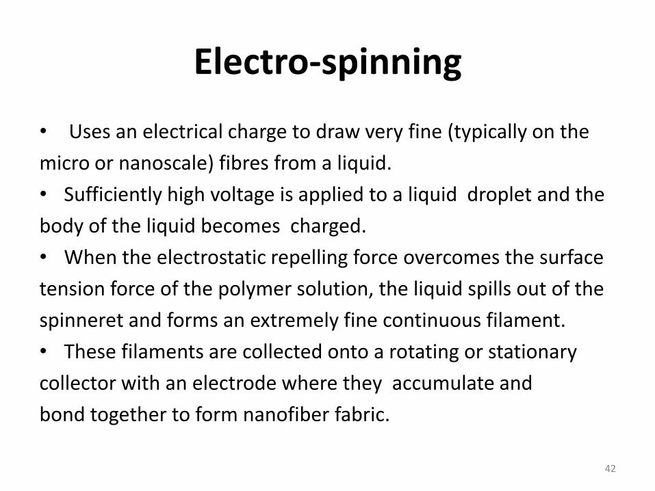
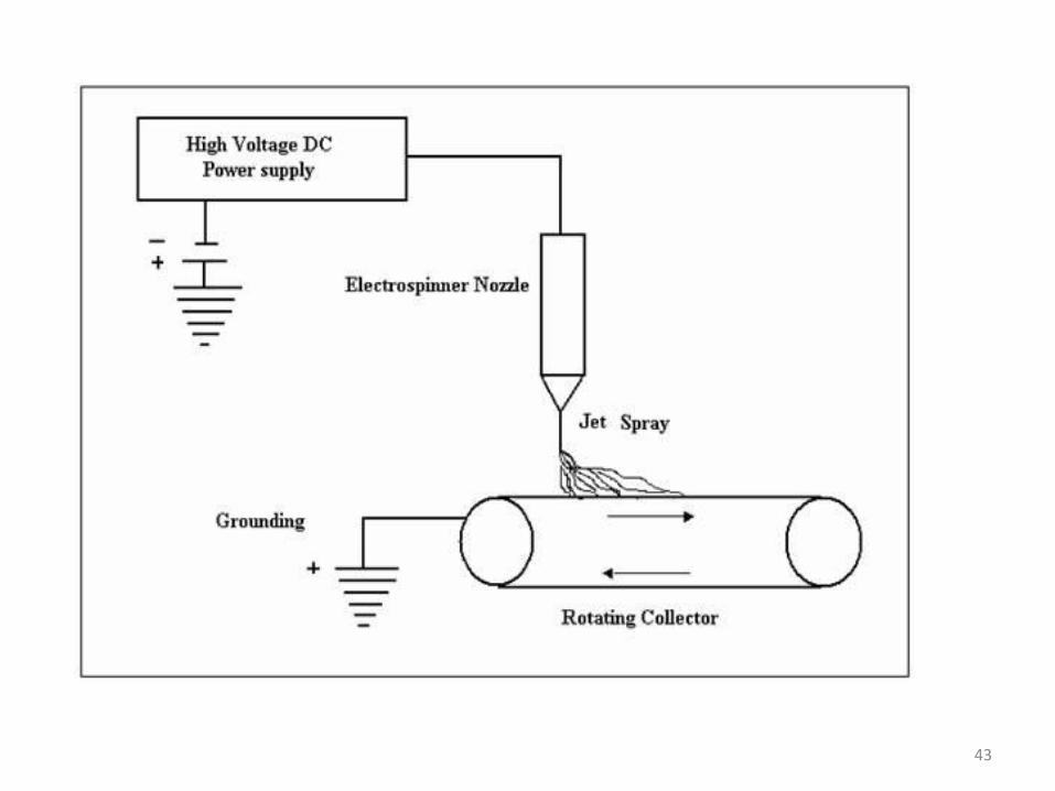
Electro-spinning
• Uses an electrical charge to draw very fine (typically on the
micro or nanoscale) fibres from a liquid.
• Sufficiently high voltage is applied to a liquid droplet and the
body of the liquid becomes charged.
• When the electrostatic repelling force overcomes the surface
tension force of the polymer solution, the liquid spills out of the
spinneret and forms an extremely fine continuous filament.
• These filaments are collected onto a rotating or stationary
collector with an electrode where they accumulate and
bond together to form nanofiber fabric.
42
43
Lithography
• Connects high proportion of the nanowires to theelectrodes,without the necessity to link the two components individually.
• It is the process of transferring geometric shapes on a mask to the surface of a silicon wafer
44

45

Using the lithographically patterned nanowire electrodeposition (LPNE) method, photolithography is used to define the position and two-dimensional trajectory of nanowires (5 nm (h) and 11 nm (w)
46

Applications of Nanowires
Nanowires are promising materials for many
novel applications for their unique geometry
and unique physical properties such as:
– electrical
– magnetic
– optical
– mechanical
47
Types of Nanowires
• Metal nanowires
• Semiconductor nanowires (Silicon nanowires)
• Oxide nanowires
• Multi-segment nanowires
• Semiconductor quantum wires
48
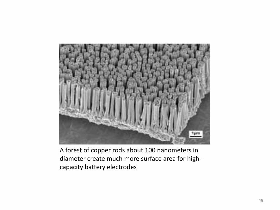
A forest of copper rods about 100 nanometers in diameter create much more surface area for high-capacity battery electrodes
49
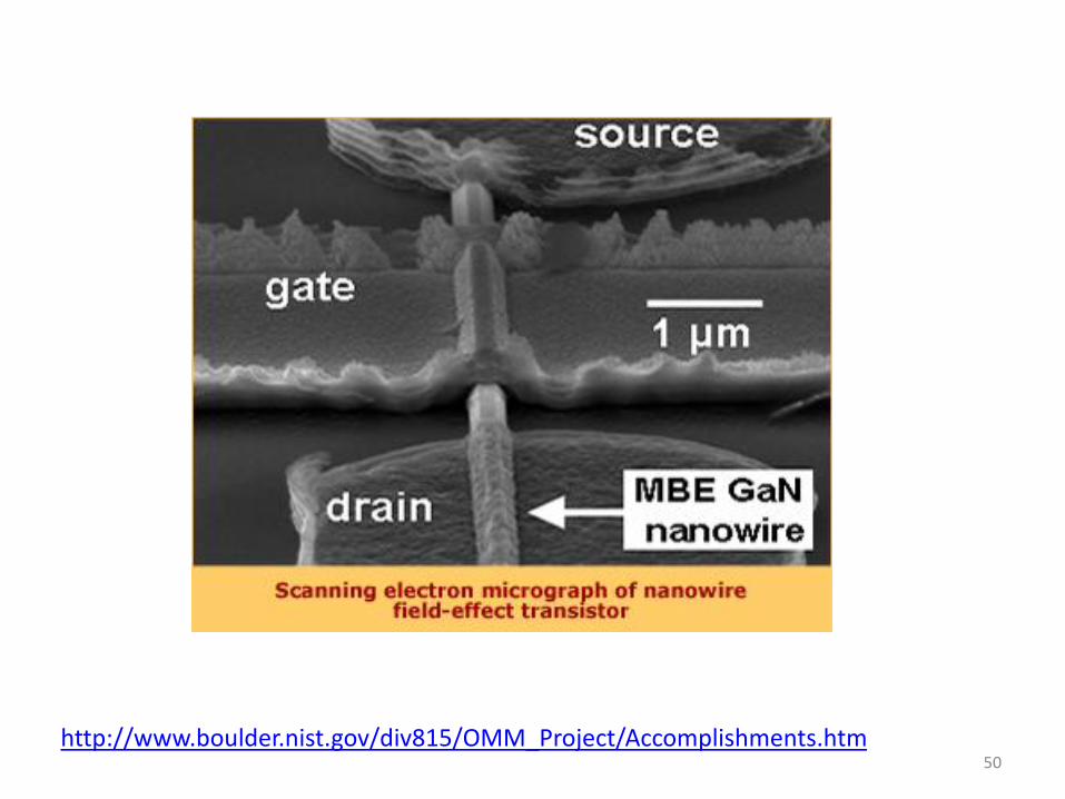
http://www.boulder.nist.gov/div815/OMM_Project/Accomplishments.htm50
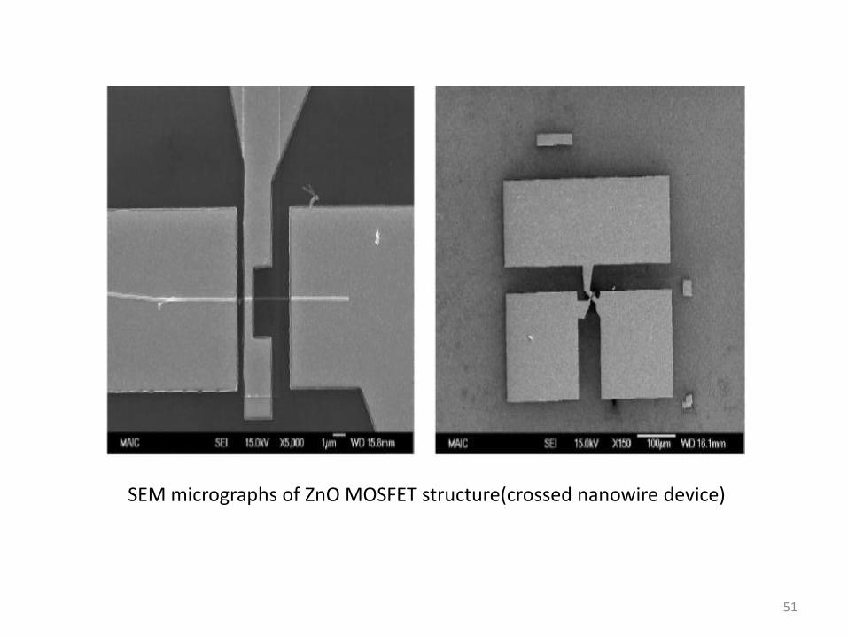
SEM micrographs of ZnO MOSFET structure(crossed nanowire device)
51
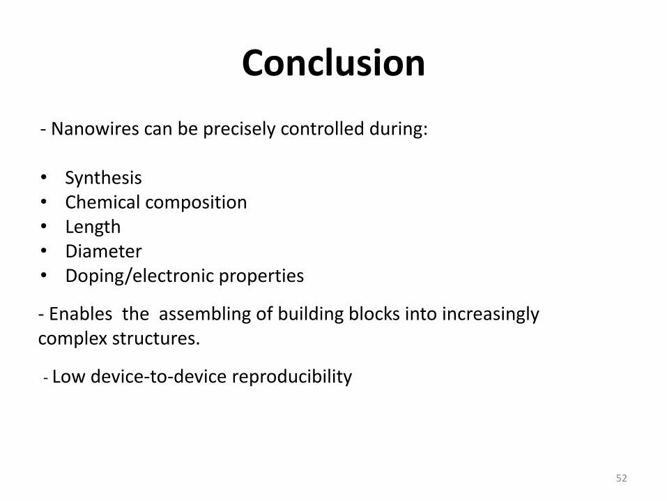
Conclusion
- Nanowires can be precisely controlled during:
• Synthesis• Chemical composition• Length• Diameter• Doping/electronic properties
- Enables the assembling of building blocks into increasingly complex structures.
- Low device-to-device reproducibility
52

REFERENCES• http://en.wikipedia.org/wiki/Potential_well• http://phycomp.technion.ac.il/~anastasy/thesis/node10.html• http://mrsec.wisc.edu/Edetc/cineplex/nanotube/index.html• http://www.chm.bris.ac.uk/webprojects2001/andrews/nanotubes-synthesis.html• http://students.chem.tue.nl/ifp03/synthesis.html• http://www.fy.chalmers.se/atom/research/nanotubes/experimental.xml• http://nanogloss.com/nanotubes/what-is-carbon-nanotube-synthesis/#axzz1NJyWPECS• http://www.personal.reading.ac.uk/~scsharip/tubes.htm• http://www.research.ibm.com/nanoscience/manipulation.html• http://eeesrikar.blogspot.com/p/ppts.html• http://www.nature.com/nnano/journal/v5/n1/fig_tab/nnano.2009.319_F1.html• http://www.ioap.tu-berlin.de/fileadmin/i5/AG_Moeller/Papers/anderes/QC_in_Ge_nanocrystals_-
_APL_84__4056__2004_.pdf• http://www.nano.ugent.be/index.php?Itemid=89&id=31&option=com_content§ionid=2&task=category• http://www.nanotech-now.com/nanotube-buckyball-sites.htm• http://www.ece.rochester.edu/courses/ECE580/docs/Quantum_Dot_Lasers.pdf• http://physics.schooltool.nl/quantumoptics/qd.php• http://www.chm.bris.ac.uk/webprojects2001/andrews/nanotubes-synthesis.html• http://students.chem.tue.nl/ifp03/synthesis.html• http://www.pharmainfo.net/reviews/methods-carbon-nanotube-and-nanohorn-synthesis-review• http://www.engr.utk.edu/mse/Textiles/Nanofiber%20Nonwovens.htm• http://www.ece.gatech.edu/research/labs/vc/theory/photolith.html• http://en.wikipedia.org/wiki/Photolithography• http://www.physicscentral.com/explore/action/lithium-links.cfm• http://focus.aps.org/story/v11/st15• http://sundoc.bibliothek.uni-halle.de/diss-online/07/07H121/prom.pdf• http://www.engr.colostate.edu/ECE581/fall07/Nanowires%20and%20Nanorods.pdf
53

THANKS FOR YOUR ATTENTION!
54