
Atmel AT89S8253 Data Sheet - Utah State University · The AT89S8253 is a low-power,...
56
Features • Compatible with MCS ® -51 Products • 12K Bytes of In-System Programmable (ISP) Flash Program Memory – SPI Serial Interface for Program Downloading – Endurance: 10,000 Write/Erase Cycles • 2K Bytes EEPROM Data Memory – Endurance: 100,000 Write/Erase Cycles • 64-byte User Signature Array • 2.7V to 5.5V Operating Range • Fully Static Operation: 0 Hz to 24 MHz • Three-level Program Memory Lock • 256 x 8-bit Internal RAM • 32 Programmable I/O Lines • Three 16-bit Timer/Counters • Nine Interrupt Sources • Enhanced UART Serial Port with Framing Error Detection and Automatic Address Recognition • Enhanced SPI (Double Write/Read Buffered) Serial Interface • Low-power Idle and Power-down Modes • Interrupt Recovery from Power-down Mode • Programmable Watchdog Timer • Dual Data Pointer • Power-off Flag • Flexible ISP Programming (Byte and Page Modes) – Page Mode: 64 Bytes/Page for Code Memory, 32 Bytes/Page for Data Memory • Four-level Enhanced Interrupt Controller • Programmable and Fuseable x2 Clock Option • Internal Power-on Reset • 42-pin PDIP Package Option for Reduced EMC Emission Description The AT89S8253 is a low-power, high-performance CMOS 8-bit microcontroller with 12K bytes of In-System Programmable (ISP) Flash program memory and 2K bytes of EEPROM data memory. The device is manufactured using Atmel’s high-density non- volatile memory technology and is compatible with the industry-standard MCS-51 instruction set and pinout. The on-chip downloadable Flash allows the program mem- ory to be reprogrammed in-system through an SPI serial interface or by a conventional nonvolatile memory programmer. By combining a versatile 8-bit CPU with download- able Flash on a monolithic chip, the Atmel AT89S8253 is a powerful microcontroller which provides a highly-flexible and cost-effective solution to many embedded control applications. The AT89S8253 provides the following standard features: 12K bytes of In-System Pro- grammable Flash, 2K bytes of EEPROM, 256 bytes of RAM, 32 I/O lines, programmable watchdog timer, two data pointers, three 16-bit timer/counters, a six- vector, four-level interrupt architecture, a full duplex serial port, on-chip oscillator, and clock circuitry. In addition, the AT89S8253 is designed with static logic for operation down to zero frequency and supports two software selectable power saving modes. The Idle Mode stops the CPU while allowing the RAM, timer/counters, serial port, and interrupt system to continue functioning. The Power-down mode saves the RAM con- tents but freezes the oscillator, disabling all other chip functions until the next external interrupt or hardware reset. The on-board Flash/EEPROM is accessible through the SPI serial interface. Holding RESET active forces the SPI bus into a serial programming interface and allows the program memory to be written to or read from, unless one or more lock bits have been activated. Rev. 3286A–MICRO–7/04 8-bit Microcontroller with 12K Bytes Flash and 2K Bytes EEPROM AT89S8253 Preliminary
Transcript of Atmel AT89S8253 Data Sheet - Utah State University · The AT89S8253 is a low-power,...
Rev. 3286A–MICRO–7/04
8-bit Microcontroller with 12K Bytes Flash and 2K Bytes EEPROM
AT89S8253
Preliminary
Features• Compatible with MCS®-51 Products• 12K Bytes of In-System Programmable (ISP) Flash Program Memory
– SPI Serial Interface for Program Downloading– Endurance: 10,000 Write/Erase Cycles
• 2K Bytes EEPROM Data Memory– Endurance: 100,000 Write/Erase Cycles
• 64-byte User Signature Array• 2.7V to 5.5V Operating Range• Fully Static Operation: 0 Hz to 24 MHz• Three-level Program Memory Lock• 256 x 8-bit Internal RAM• 32 Programmable I/O Lines• Three 16-bit Timer/Counters• Nine Interrupt Sources• Enhanced UART Serial Port with Framing Error Detection and Automatic Address
Recognition• Enhanced SPI (Double Write/Read Buffered) Serial Interface• Low-power Idle and Power-down Modes• Interrupt Recovery from Power-down Mode• Programmable Watchdog Timer• Dual Data Pointer• Power-off Flag• Flexible ISP Programming (Byte and Page Modes)
– Page Mode: 64 Bytes/Page for Code Memory, 32 Bytes/Page for Data Memory• Four-level Enhanced Interrupt Controller• Programmable and Fuseable x2 Clock Option• Internal Power-on Reset• 42-pin PDIP Package Option for Reduced EMC Emission
DescriptionThe AT89S8253 is a low-power, high-performance CMOS 8-bit microcontroller with12K bytes of In-System Programmable (ISP) Flash program memory and 2K bytes ofEEPROM data memory. The device is manufactured using Atmel’s high-density non-volatile memory technology and is compatible with the industry-standard MCS-51instruction set and pinout. The on-chip downloadable Flash allows the program mem-ory to be reprogrammed in-system through an SPI serial interface or by a conventionalnonvolatile memory programmer. By combining a versatile 8-bit CPU with download-able Flash on a monolithic chip, the Atmel AT89S8253 is a powerful microcontrollerwhich provides a highly-flexible and cost-effective solution to many embedded controlapplications.The AT89S8253 provides the following standard features: 12K bytes of In-System Pro-grammable Flash, 2K bytes of EEPROM, 256 bytes of RAM, 32 I/O l ines,programmable watchdog timer, two data pointers, three 16-bit timer/counters, a six-vector, four-level interrupt architecture, a full duplex serial port, on-chip oscillator, andclock circuitry. In addition, the AT89S8253 is designed with static logic for operationdown to zero frequency and supports two software selectable power saving modes.The Idle Mode stops the CPU while allowing the RAM, timer/counters, serial port, andinterrupt system to continue functioning. The Power-down mode saves the RAM con-tents but freezes the oscillator, disabling all other chip functions until the next externalinterrupt or hardware reset.The on-board Flash/EEPROM is accessible through the SPI serial interface. HoldingRESET active forces the SPI bus into a serial programming interface and allows theprogram memory to be written to or read from, unless one or more lock bits have beenactivated.
1

Pin ConfigurationsPDIP
TQFP
1234567891011121314151617181920
4039383736353433323130292827262524232221
(T2) P1.0(T2 EX) P1.1
P1.2P1.3
(SS) P1.4(MOSI) P1.5(MISO) P1.6(SCK) P1.7
RST(RXD) P3.0(TXD) P3.1(INT0) P3.2(INT1) P3.3
(T0) P3.4(T1) P3.5
(WR) P3.6(RD) P3.7
XTAL2XTAL1
GND
VCCP0.0 (AD0)P0.1 (AD1)P0.2 (AD2)P0.3 (AD3)P0.4 (AD4)P0.5 (AD5)P0.6 (AD6)P0.7 (AD7)EA/VPPALE/PROGPSENP2.7 (A15)P2.6 (A14)P2.5 (A13)P2.4 (A12)P2.3 (A11)P2.2 (A10)P2.1 (A9)P2.0 (A8)
1234567891011
3332313029282726252423
44 43 42 41 40 39 38 37 36 35 34
12 13 14 15 16 17 18 19 20 21 22
(MOSI) P1.5(MISO) P1.6(SCK) P1.7
RST(RXD) P3.0
NC(TXD) P3.1(INT0) P3.2(INT1) P3.3
(T0) P3.4(T1) P3.5
P0.4 (AD4)P0.5 (AD5)P0.6 (AD6)P0.7 (AD7)EA/VPPNCALE/PROGPSENP2.7 (A15)P2.6 (A14)P2.5 (A13)
P1.
4 (S
S)
P1.
3P
1.2
P1.
1 (T
2 E
X)
P1.
0 (T
2)N
CV
CC
P0.
0 (A
D0)
P0.
1 (A
D1)
P0.
2 (A
D2)
P0.
3 (A
D3)
(WR
) P
3.6
(RD
) P
3.7
XT
AL2
XT
AL1
GN
DG
ND
(A8)
P2.
0(A
9) P
2.1
(A10
) P
2.2
(A11
) P
2.3
(A12
) P
2.4
2 AT89S8253 [Preliminary]
PLCC
PDIP
7891011121314151617
3938373635343332313029
(MOSI) P1.5(MISO) P1.6(SCK) P1.7
RST(RXD) P3.0
NC(TXD) P3.1(INT0) P3.2(INT1) P3.3
(T0) P3.4(T1) P3.5
P0.4 (AD4)P0.5 (AD5)P0.6 (AD6)P0.7 (AD7)EA/VPPNCALE/PROGPSENP2.7 (A15)P2.6 (A14)P2.5 (A13)
6 5 4 3 2 1 44 43 42 41 40
18 19 20 21 22 23 24 25 26 27 28
(WR
) P
3.6
(RD
) P
3.7
XT
AL2
XT
AL1
GN
DN
C(A
8) P
2.0
(A9)
P2.
1(A
10)
P2.
2(A
11)
P2.
3(A
12)
P2.
4
P1.
4 (S
S)
P1.
3P
1.2
P1.
1 (T
2 E
X)
P1.
0 (T
2)N
CV
CC
P0.
0 (A
D0)
P0.
1 (A
D1)
P0.
2 (A
D2)
P0.
3 (A
D3)
123456789101112131415161718192021
424140393837363534333231302928272625242322
RST(RXD) P3.0(TXD) P3.1(INT0) P3.2(INT1) P3.3
(T0) P3.4(T1) P3.5
(WR) P3.6(RD) P3.7
XTAL2XTAL1
GNDPWRGND(A8) P2.0(A9) P2.1
(A10) P2.2(A11) P2.3(A12) P2.4(A13) P2.5(A14) P2.6(A15) P2.7
P1.7 (SCK)P1.6 (MISO)P1.5 (MOSI)P1.4 (SS)P1.3P1.2P1.1 (T2EX)P1.0 (T2)VDDPWRVDDP0.0 (AD0)P0.1 (AD1)P0.2 (AD2)P0.3 (AD3)P0.4 (AD4)P0.5 (AD5)P0.6 (AD6)P0.7 (AD7)EA/VPPALE/PROGPSEN
3286A–MICRO–7/04
AT89S8253 [Preliminary]
Pin Description
VCC Supply voltage (all packages except 42-PDIP).
GND Ground (all packages except 42-PDIP; for 42-PDIP GND connects only the logic core and theembedded program/data memories).
VDD Supply voltage for the 42-PDIP which connects only the logic core and the embedded pro-gram/data memories.
PWRVDD Supply voltage for the 42-PDIP which connects only the I/O Pad Drivers.
The application board must connect both VDD and PWRVDD to the board supply voltage.
PWRGND Ground for the 42-PDIP which connects only the I/O Pad Drivers. PWRGND and GND areweakly connected through the common silicon substrate, but not through any metal links. Theapplication board must connect both GND and PWRGND to the board ground.
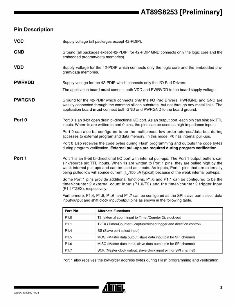
Port 0 Port 0 is an 8-bit open drain bi-directional I/O port. As an output port, each pin can sink six TTLinputs. When 1s are written to port 0 pins, the pins can be used as high-impedance inputs.
Port 0 can also be configured to be the multiplexed low-order address/data bus duringaccesses to external program and data memory. In this mode, P0 has internal pull-ups.
Port 0 also receives the code bytes during Flash programming and outputs the code bytesduring program verification. External pull-ups are required during program verification.
Port 1 Port 1 is an 8-bit bi-directional I/O port with internal pull-ups. The Port 1 output buffers cansink/source six TTL inputs. When 1s are written to Port 1 pins, they are pulled high by theweak internal pull-ups and can be used as inputs. As inputs, Port 1 pins that are externallybeing pulled low will source current (IIL,150 µA typical) because of the weak internal pull-ups.
Some Port 1 pins provide additional functions. P1.0 and P1.1 can be configured to be thetimer/counter 2 external count input (P1.0/T2) and the timer/counter 2 trigger input(P1.1/T2EX), respectively.
Furthermore, P1.4, P1.5, P1.6, and P1.7 can be configured as the SPI slave port select, datainput/output and shift clock input/output pins as shown in the following table.
Port 1 also receives the low-order address bytes during Flash programming and verification.
Port Pin Alternate Functions
P1.0 T2 (external count input to Timer/Counter 2), clock-out
P1.1 T2EX (Timer/Counter 2 capture/reload trigger and direction control)
P1.4 SS (Slave port select input)
P1.5 MOSI (Master data output, slave data input pin for SPI channel)
P1.6 MISO (Master data input, slave data output pin for SPI channel)
P1.7 SCK (Master clock output, slave clock input pin for SPI channel)
33286A–MICRO–7/04
Port 2 Port 2 is an 8-bit bi-directional I/O port with internal pull-ups. The Port 2 output buffers cansink/source six TTL inputs. When 1s are written to Port 2 pins, they are pulled high by theweak internal pull-ups and can be used as inputs. As inputs, Port 2 pins that are externallybeing pulled low will source current (IIL,150 µA typical) because of the weak internal pull-ups.
Port 2 emits the high-order address byte during fetches from external program memory andduring accesses to external data memory that use 16-bit addresses (MOVX @ DPTR). In thisapplication, Port 2 uses strong internal pull-ups when emitting 1s. During accesses to externaldata memory that use 8-bit addresses (MOVX @ RI), Port 2 emits the contents of the P2Special Function Register.
Port 2 also receives the high-order address bits and some control signals during Flashprogramming and verification.
Port 3 Port 3 is an 8-bit bi-directional I/O port with internal pull-ups. The Port 3 output buffers cansink/source six TTL inputs. When 1s are written to Port 3 pins, they are pulled high by theweak internal pull-ups and can be used as inputs. As inputs, Port 3 pins that are externallybeing pulled low will source current (IIL,150 µA typical) because of the weak internal pull-ups.
Port 3 receives some control signals for Flash programming and verification.
Port 3 also serves the functions of various special features of the AT89S8253, as shown in thefollowing table.
Note: 1. All pins in ports 1 and 2 and almost all pins in port 3 (the exceptions are P3.2 INT0 and P3.3INT1) have their weak internal pull-ups disabled in the Power-down mode. Port pins P3.2(INT0) and P3.1 (INT1) are active even in Power-down mode (to be able to sense aninterrupt request to exit the Power-down mode) and as such still have their weak internalpull-ups turned on.
RST Reset input. A high on this pin for at least two machine cycles while the oscillator is runningresets the device.
ALE/PROG Address Latch Enable. ALE/PROG is an output pulse for latching the low byte of the address(on its falling edge) during accesses to external memory. This pin is also the program pulseinput (PROG) during Flash programming.
In normal operation, ALE is emitted at a constant rate of 1/6 the oscillator frequency and maybe used for external timing or clocking purposes. Note, however, that one ALE pulse isskipped during each access to external data memory.
Port Pin Alternate Functions
P3.0 RXD (serial input port)
P3.1 TXD (serial output port)
P3.2 INT0 (external interrupt 0)(1)
P3.3 INT1 (external interrupt 1)(1)
P3.4 T0 (timer 0 external input)
P3.5 T1 (timer 1 external input)
P3.6 WR (external data memory write strobe)
P3.7 RD (external data memory read strobe)
4 AT89S8253 [Preliminary]3286A–MICRO–7/04

AT89S8253 [Preliminary]
If desired, ALE operation can be disabled by setting bit 0 of the AUXR SFR at location 8EH.With the bit set, ALE is active only during a MOVX or MOVC instruction. Otherwise, the pin isweakly pulled high. Setting the ALE-disable bit has no effect if the microcontroller is in externalexecution mode.
PSEN Program Store Enable. PSEN is the read strobe to external program memory (active low).
When the AT89S8253 is executing code from external program memory, PSEN is activatedtwice each machine cycle, except that two PSEN activations are skipped during each accessto external data memory.
EA/VPP External Access Enable. EA must be strapped to GND in order to enable the device to fetchcode from external program memory locations starting at 0000H up to FFFFH. Note, however,that if lock bit 1 is programmed, EA will be internally latched on reset.
EA should be strapped to VCC for internal program executions. This pin also receives the12-volt programming enable voltage (VPP) during Flash programming when 12-volt program-ming is selected.
XTAL1 Input to the inverting oscillator amplifier and input to the internal clock operating circuit.
XTAL2 Output from the inverting oscillator amplifier.
53286A–MICRO–7/04
Block Diagram
PORT 2 DRIVERS
PORT 2LATCH
P2.0 - P2.7
FLASHPORT 0LATCHRAMEEPROM
PROGRAMADDRESSREGISTER
BUFFER
PCINCREMENTER
PROGRAMCOUNTER
DUALDPTR
INSTRUCTIONREGISTER
BREGISTER
INTERRUPT, SERIAL PORT,AND TIMER BLOCKS
STACKPOINTERACC
TMP2 TMP1
ALU
PSW
TIMINGAND
CONTROL
PORT 1 DRIVERS
P1.0 - P1.7
PORT 3LATCH
PORT 3 DRIVERS
P3.0 - P3.7
OSC
GND
VCC
PSEN
ALE/PROG
EA / VPP
RST
RAM ADDR.REGISTER
PORT 0 DRIVERS
P0.0 - P0.7
PORT 1LATCH
WATCHDOG
SPIPORT
PROGRAMLOGIC
6 AT89S8253 [Preliminary]3286A–MICRO–7/04
AT89S8253 [Preliminary]
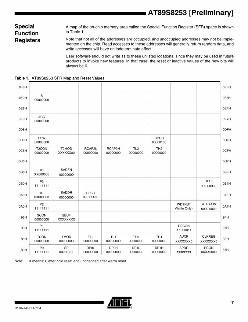
Special Function Registers
A map of the on-chip memory area called the Special Function Register (SFR) space is shownin Table 1.
Note that not all of the addresses are occupied, and unoccupied addresses may not be imple-mented on the chip. Read accesses to these addresses will generally return random data, andwrite accesses will have an indeterminate effect.
User software should not write 1s to these unlisted locations, since they may be used in futureproducts to invoke new features. In that case, the reset or inactive values of the new bits willalways be 0.
Note: # means: 0 after cold reset and unchanged after warm reset.
Table 1. AT89S8253 SFR Map and Reset Values
0F8H 0FFH
0F0HB
000000000F7H
0E8H 0EFH
0E0HACC
000000000E7H
0D8H 0DFH
0D0HPSW
00000000SPCR
000001000D7H
0C8HT2CON
00000000T2MOD
XXXXXX00RCAP2L
00000000RCAP2H00000000
TL200000000
TH200000000
0CFH
0C0H 0C7H
0B8HIP
XX000000SADEN
000000000BFH
0B0HP3
11111111IPH
XX0000000B7H
0A8HIE
0X000000SADDR
00000000SPSR
000XXX000AFH
0A0HP2
11111111WDTRST
(Write Only)WDTCON
0000 00000A7H
98HSCON
00000000SBUF
XXXXXXXX9FH
90HP1
11111111EECON
XX00001197H
88HTCON
00000000TMOD
00000000TL0
00000000TL1
00000000TH0
00000000TH1
00000000AUXR
XXXXXXX0
CLKREG
XXXXXXX08FH
80HP0
11111111SP
00000111DP0L
00000000DP0H
00000000DP1L
00000000DP1H
00000000SPDR
########PCON
0XXX000087H
73286A–MICRO–7/04

Auxiliary Register The AUXR Register contains a single active bit called DISALE.
Clock Register The CLKREG register contains a single active bit called X2.
SPI Registers Control and status bits for the Serial Peripheral Interface are contained in registers SPCR (seeTable 11 on page 25) and SPSR (see Table 12 on page 26). The SPI data bits are containedin the SPDR register. In normal SPI mode, writing the SPI data register during serial datatransfer sets the Write Collision bit (WCOL) in the SPSR register. In enhanced SPI mode, theSPDR is also write double-buffered because WCOL works as a Write Buffer Full Flag insteadof being a collision flag. The values in SPDR are not changed by Reset.
Interrupt Registers The global interrupt enable bit and the individual interrupt enable bits are in the IE register. Inaddition, the individual interrupt enable bit for the SPI is in the SPCR register. Four prioritiescan be set for each of the six interrupt sources in the IP and IPH registers.
IPH bits have the same functions as IP bits, except IPH has higher priority than IP. By usingIPH in conjunction with IP, a priority level of 0, 1, 2, or 3 may be set for each interrupt.
Dual Data Pointer Registers
To facilitate accessing both internal EEPROM and external data memory, two banks of 16-bitData Pointer Registers are provided: DP0 at SFR address locations 82H - 83H and DP1 at84H - 85H. Bit DPS = 0 in SFR WMCON selects DP0 and DPS = 1 selects DP1. The usershould ALWAYS initialize the DPS bit to the appropriate value before accessing the respectiveData Pointer Register.
Table 2. AUXR – Auxiliary Register
AUXR Address = 8EH Reset Value = XXXX XXX0B
Not Bit Addressable
– – – – – – – DISALE
Bit 7 6 5 4 3 2 1 0
Symbol Function
DISALE When DISALE = 0, ALE is emitted at a constant rate of 1/6 the oscillator frequency (except during MOVX when 1 ALE pulse is missing). When DISALE = 1, ALE is active only during a MOVX or MOVC instruction.
Table 3. CLKREG – Clock Register
CLKREG Address = 8FH Reset Value = XXXX XXX0B
Not Bit Addressable
– – – – – – – X2
Bit 7 6 5 4 3 2 1 0
Symbol Function
X2 When X2 = 0, the oscillator frequency (at XTAL1 pin) is internally divided by 2 before it is used as the device system frequency.When X2 = 1, the divider by 2 is no longer used and the XTAL1 frequency becomes the device system frequency. This enables the user to choose a 6 MHz crystal instead of a 12 MHz crystal, for example, in order to reduce EMI.
8 AT89S8253 [Preliminary]3286A–MICRO–7/04
AT89S8253 [Preliminary]
Power Off Flag The Power Off Flag (POF), located at bit_4 (PCON.4) in the PCON SFR. POF, is set to “1”during power up. It can be set and reset under software control and is not affected by RESET.
Data Memory – EEPROM and RAM
The AT89S8253 implements 2K bytes of on-chip EEPROM for data storage and 256 bytes ofRAM. The upper 128 bytes of RAM occupy a parallel space to the Special Function Registers.That means the upper 128 bytes have the same addresses as the SFR space but are physi-cally separate from SFR space.
When an instruction accesses an internal location above address 7FH, the address modeused in the instruction specifies whether the CPU accesses the upper 128 bytes of RAM or theSFR space. Instructions that use direct addressing access the SFR space.
For example, the following direct addressing instruction accesses the SFR at location 0A0H(which is P2).
MOV 0A0H, #data
Instructions that use indirect addressing access the upper 128 bytes of RAM. For example, thefollowing indirect addressing instruction, where R0 contains 0A0H, accesses the data byte ataddress 0A0H, rather than P2 (whose address is 0A0H).
MOV @R0, #data
Note that stack operations are examples of indirect addressing, so the upper 128 bytes of dataRAM are available as stack space.
The on-chip EEPROM data memory is selected by setting the EEMEN bit in the EECON regis-ter at SFR address location 96H. The EEPROM address range is from 000H to 7FFH. MOVXinstructions are used to access the EEPROM. To access off-chip data memory with the MOVXinstructions, the EEMEN bit needs to be set to “0”.
The EEMWE bit in the EECON register needs to be set to “1” before any byte location in theEEPROM can be written. User software should reset EEMWE bit to “0” if no further EEPROMwrite is required. EEPROM write cycles in the serial programming mode are self-timed andtypically take 4 ms. The progress of EEPROM write can be monitored by reading theRDY/BSY bit (read-only) in SFR EECON. RDY/BSY = 0 means programming is still inprogress and RDY/BSY = 1 means an EEPROM write cycle is completed and another writecycle can be initiated. Bit EELD in EECON controls whether the next MOVX instruction willonly load the write buffer of the EEPROM or will actually start the programming cycle. By set-ting EELD, only load will occur. Before the last MOVX in a given page of 32 bytes, EELDshould be cleared so that after the last MOVX the entire page will be programmed at the sametime. This way, 32 bytes will only require 4 ms of programming time instead of 128 msrequired in single byte programming.
In addition, during EEPROM programming, an attempted read from the EEPROM will fetch thebyte being written with the MSB complemented. Once the write cycle is completed, true dataare valid at all bit locations.
93286A–MICRO–7/04
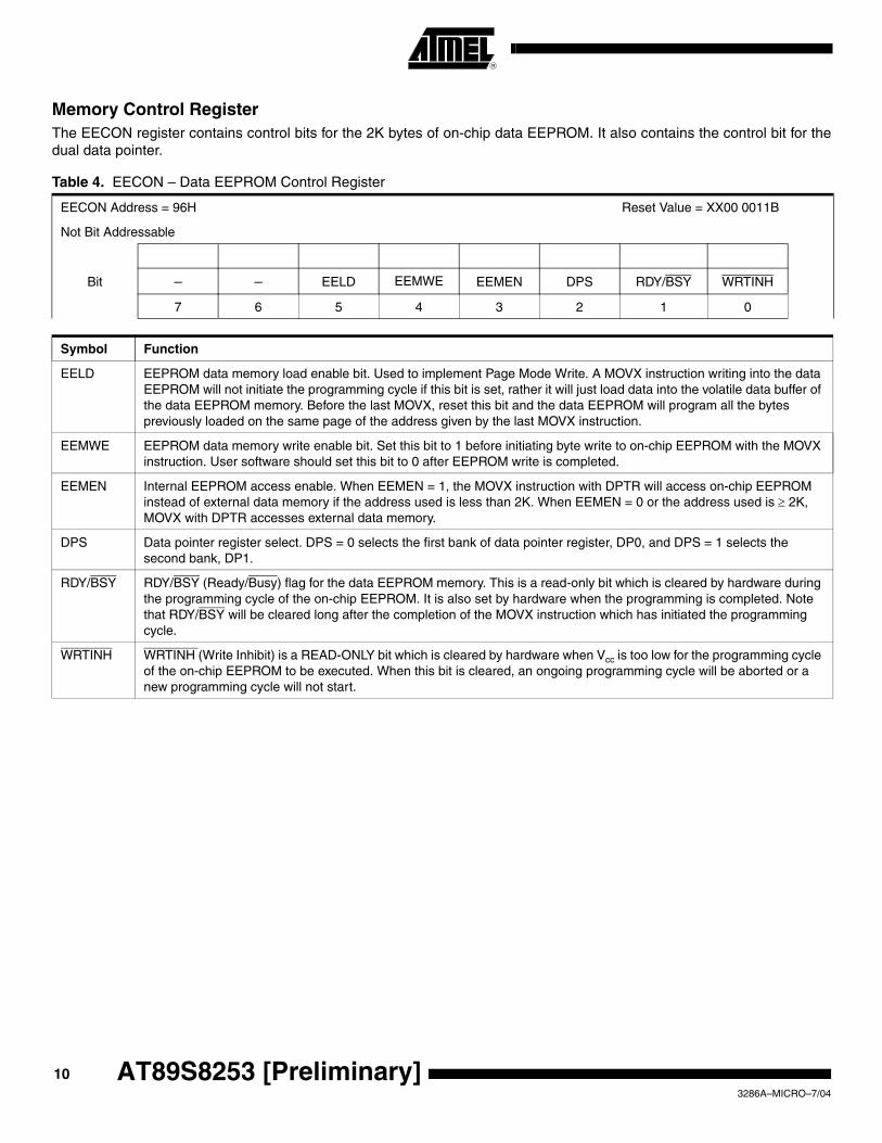
Memory Control RegisterThe EECON register contains control bits for the 2K bytes of on-chip data EEPROM. It also contains the control bit for thedual data pointer.
Table 4. EECON – Data EEPROM Control Register
EECON Address = 96H Reset Value = XX00 0011B
Not Bit Addressable
Bit – – EELD EEMWE EEMEN DPS RDY/BSY WRTINH
7 6 5 4 3 2 1 0
Symbol Function
EELD EEPROM data memory load enable bit. Used to implement Page Mode Write. A MOVX instruction writing into the data EEPROM will not initiate the programming cycle if this bit is set, rather it will just load data into the volatile data buffer of the data EEPROM memory. Before the last MOVX, reset this bit and the data EEPROM will program all the bytes previously loaded on the same page of the address given by the last MOVX instruction.
EEMWE EEPROM data memory write enable bit. Set this bit to 1 before initiating byte write to on-chip EEPROM with the MOVX instruction. User software should set this bit to 0 after EEPROM write is completed.
EEMEN Internal EEPROM access enable. When EEMEN = 1, the MOVX instruction with DPTR will access on-chip EEPROM instead of external data memory if the address used is less than 2K. When EEMEN = 0 or the address used is ≥ 2K, MOVX with DPTR accesses external data memory.
DPS Data pointer register select. DPS = 0 selects the first bank of data pointer register, DP0, and DPS = 1 selects the second bank, DP1.
RDY/BSY RDY/BSY (Ready/Busy) flag for the data EEPROM memory. This is a read-only bit which is cleared by hardware during the programming cycle of the on-chip EEPROM. It is also set by hardware when the programming is completed. Note that RDY/BSY will be cleared long after the completion of the MOVX instruction which has initiated the programming cycle.
WRTINH WRTINH (Write Inhibit) is a READ-ONLY bit which is cleared by hardware when Vcc is too low for the programming cycle of the on-chip EEPROM to be executed. When this bit is cleared, an ongoing programming cycle will be aborted or a new programming cycle will not start.
10 AT89S8253 [Preliminary]3286A–MICRO–7/04
AT89S8253 [Preliminary]
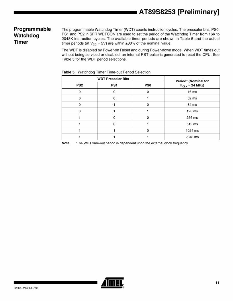
Programmable Watchdog Timer
The programmable Watchdog Timer (WDT) counts instruction cycles. The prescaler bits, PS0,PS1 and PS2 in SFR WDTCON are used to set the period of the Watchdog Timer from 16K to2048K instruction cycles. The available timer periods are shown in Table 5 and the actualtimer periods (at VCC = 5V) are within ±30% of the nominal value.
The WDT is disabled by Power-on Reset and during Power-down mode. When WDT times outwithout being serviced or disabled, an internal RST pulse is generated to reset the CPU. SeeTable 5 for the WDT period selections.
Note: *The WDT time-out period is dependent upon the external clock frequency.
Table 5. Watchdog Timer Time-out Period Selection
WDT Prescaler BitsPeriod* (Nominal for
FCLK = 24 MHz)PS2 PS1 PS0
0 0 0 16 ms
0 0 1 32 ms
0 1 0 64 ms
0 1 1 128 ms
1 0 0 256 ms
1 0 1 512 ms
1 1 0 1024 ms
1 1 1 2048 ms
113286A–MICRO–7/04

Watchdog Control Register
The WDTCON register contains control bits for the Watchdog Timer (shown in Table 6).
Table 6. WDTCON – Watchdog Control Register
WDTCON Address = A7H Reset Value = 0000 0000B
Not Bit Addressable
PS2 PS1 PS0 WDIDLE DISRTO HWDT WSWRST WDTEN
Bit 7 6 5 4 3 2 1 0
Symbol Function
PS2PS1PS0
Prescaler bits for the watchdog timer (WDT). When all three bits are cleared to 0, the watchdog timer has a nominal period of 16K machine cycles, (i.e. 16 ms at a XTAL frequency of 24 MHz in normal mode). When all three bits are set to 1, the nominal period is 2048K machine cycles, (i.e. 2048 ms at 24 MHz clock frequency).
WDIDLE Disable/enable the Watchdog Timer in IDLE mode. When WDIDLE = 0, WDT continues to count in IDLE mode. When WDIDLE = 1, WDT freezes while the device is in IDLE mode.
DISRTO Disable/enable the WDT-driven Reset Out (WDT drives the RST pin). When DISRTO = 0, the RST pin is driven high after WDT times out and the entire board is reset. When DISRTO = 1, the RST pin remains only as an input and the WDT resets only the microcontroller internally after WDT times out.
HWDT Hardware mode select for the WDT. When HWDT = 0, the WDT can be turned on/off by simply setting or clearing WDTEN in the same register (this is the software mode for WDT). When HWDT = 1, the WDT has to be set by writing the sequence 1EH/E1H to the WDTRST register (with address 0A6H) and after being set in this way, WDT cannot be turned off except by reset, warm or cold (this is the hardware mode for WDT). To prevent the hardware WDT from resetting the entire device, the same sequence 1EH/E1H must be written to the same WDTRST SFR before the timeout interval.
WSWRST Watchdog software reset bit. When HWDT = 0 (i.e. WDT is in software controlled mode), this bit resets WDT. After being set by software, WSWRST is reset by hardware during the next machine cycle. If HWDT = 1, this bit has no effect, and if set by software, it will not be cleared by hardware.
WDTEN Watchdog software enable bit. When HWDT = 0 (i.e. WDT is in software-controlled mode), this bit enables WDT when set to 1 and disables WDT when cleared to 0 (it does not reset WDT in this case, but just freezes the existing counter state). If HWDT = 1, this bit is READ-ONLY and reflects the status of the WDT (whether it is running or not).
12 AT89S8253 [Preliminary]3286A–MICRO–7/04
AT89S8253 [Preliminary]
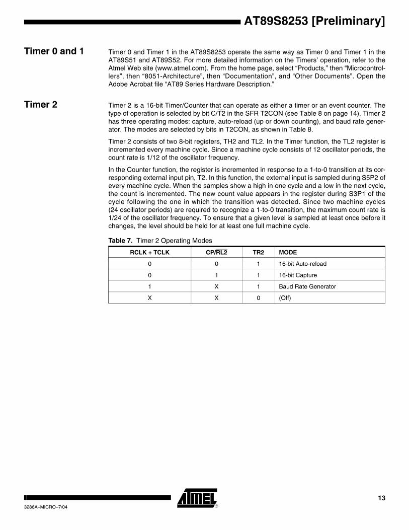
Timer 0 and 1 Timer 0 and Timer 1 in the AT89S8253 operate the same way as Timer 0 and Timer 1 in theAT89S51 and AT89S52. For more detailed information on the Timers’ operation, refer to theAtmel Web site (www.atmel.com). From the home page, select “Products,” then “Microcontrol-lers”, then “8051-Architecture”, then “Documentation”, and “Other Documents”. Open theAdobe Acrobat file “AT89 Series Hardware Description.”
Timer 2 Timer 2 is a 16-bit Timer/Counter that can operate as either a timer or an event counter. Thetype of operation is selected by bit C/T2 in the SFR T2CON (see Table 8 on page 14). Timer 2has three operating modes: capture, auto-reload (up or down counting), and baud rate gener-ator. The modes are selected by bits in T2CON, as shown in Table 8.
Timer 2 consists of two 8-bit registers, TH2 and TL2. In the Timer function, the TL2 register isincremented every machine cycle. Since a machine cycle consists of 12 oscillator periods, thecount rate is 1/12 of the oscillator frequency.
In the Counter function, the register is incremented in response to a 1-to-0 transition at its cor-responding external input pin, T2. In this function, the external input is sampled during S5P2 ofevery machine cycle. When the samples show a high in one cycle and a low in the next cycle,the count is incremented. The new count value appears in the register during S3P1 of thecycle following the one in which the transition was detected. Since two machine cycles(24 oscillator periods) are required to recognize a 1-to-0 transition, the maximum count rate is1/24 of the oscillator frequency. To ensure that a given level is sampled at least once before itchanges, the level should be held for at least one full machine cycle.
Table 7. Timer 2 Operating Modes
RCLK + TCLK CP/RL2 TR2 MODE
0 0 1 16-bit Auto-reload
0 1 1 16-bit Capture
1 X 1 Baud Rate Generator
X X 0 (Off)
133286A–MICRO–7/04
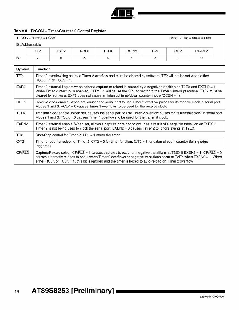
Table 8. T2CON – Timer/Counter 2 Control Register
T2CON Address = 0C8H Reset Value = 0000 0000B
Bit Addressable
TF2 EXF2 RCLK TCLK EXEN2 TR2 C/T2 CP/RL2
Bit 7 6 5 4 3 2 1 0
Symbol Function
TF2 Timer 2 overflow flag set by a Timer 2 overflow and must be cleared by software. TF2 will not be set when either RCLK = 1 or TCLK = 1.
EXF2 Timer 2 external flag set when either a capture or reload is caused by a negative transition on T2EX and EXEN2 = 1. When Timer 2 interrupt is enabled, EXF2 = 1 will cause the CPU to vector to the Timer 2 interrupt routine. EXF2 must be cleared by software. EXF2 does not cause an interrupt in up/down counter mode (DCEN = 1).
RCLK Receive clock enable. When set, causes the serial port to use Timer 2 overflow pulses for its receive clock in serial port Modes 1 and 3. RCLK = 0 causes Timer 1 overflows to be used for the receive clock.
TCLK Transmit clock enable. When set, causes the serial port to use Timer 2 overflow pulses for its transmit clock in serial port Modes 1 and 3. TCLK = 0 causes Timer 1 overflows to be used for the transmit clock.
EXEN2 Timer 2 external enable. When set, allows a capture or reload to occur as a result of a negative transition on T2EX if Timer 2 is not being used to clock the serial port. EXEN2 = 0 causes Timer 2 to ignore events at T2EX.
TR2 Start/Stop control for Timer 2. TR2 = 1 starts the timer.
C/T2 Timer or counter select for Timer 2. C/T2 = 0 for timer function. C/T2 = 1 for external event counter (falling edge triggered).
CP/RL2 Capture/Reload select. CP/RL2 = 1 causes captures to occur on negative transitions at T2EX if EXEN2 = 1. CP/RL2 = 0 causes automatic reloads to occur when Timer 2 overflows or negative transitions occur at T2EX when EXEN2 = 1. When either RCLK or TCLK = 1, this bit is ignored and the timer is forced to auto-reload on Timer 2 overflow.
14 AT89S8253 [Preliminary]3286A–MICRO–7/04
AT89S8253 [Preliminary]
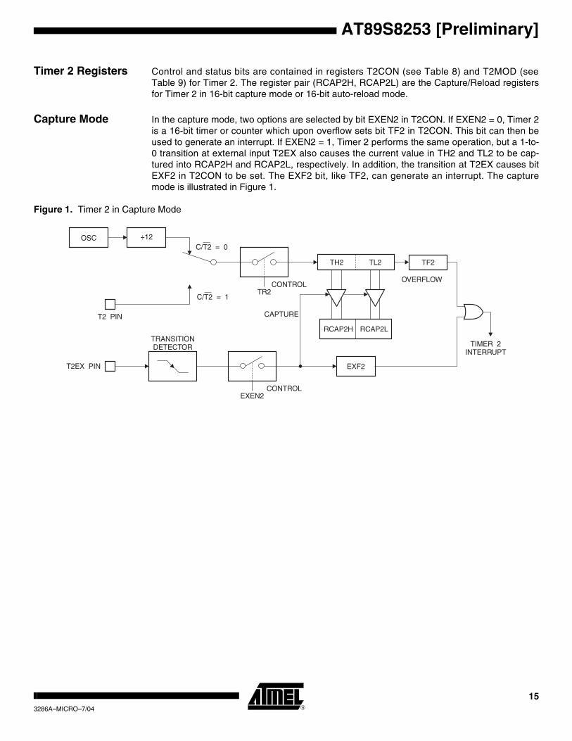
Timer 2 Registers Control and status bits are contained in registers T2CON (see Table 8) and T2MOD (seeTable 9) for Timer 2. The register pair (RCAP2H, RCAP2L) are the Capture/Reload registersfor Timer 2 in 16-bit capture mode or 16-bit auto-reload mode.
Capture Mode In the capture mode, two options are selected by bit EXEN2 in T2CON. If EXEN2 = 0, Timer 2is a 16-bit timer or counter which upon overflow sets bit TF2 in T2CON. This bit can then beused to generate an interrupt. If EXEN2 = 1, Timer 2 performs the same operation, but a 1-to-0 transition at external input T2EX also causes the current value in TH2 and TL2 to be cap-tured into RCAP2H and RCAP2L, respectively. In addition, the transition at T2EX causes bitEXF2 in T2CON to be set. The EXF2 bit, like TF2, can generate an interrupt. The capturemode is illustrated in Figure 1.
Figure 1. Timer 2 in Capture Mode
OSC
EXF2T2EX PIN
T2 PIN
TR2
EXEN2
C/T2 = 0
C/T2 = 1
CONTROL
CAPTURE
OVERFLOW
CONTROL
TRANSITIONDETECTOR TIMER 2
INTERRUPT
÷12
RCAP2LRCAP2H
TH2 TL2 TF2
153286A–MICRO–7/04
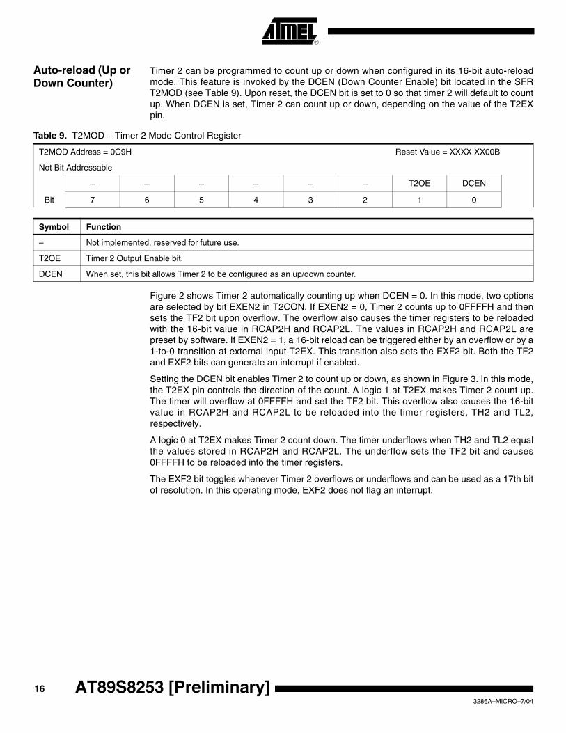
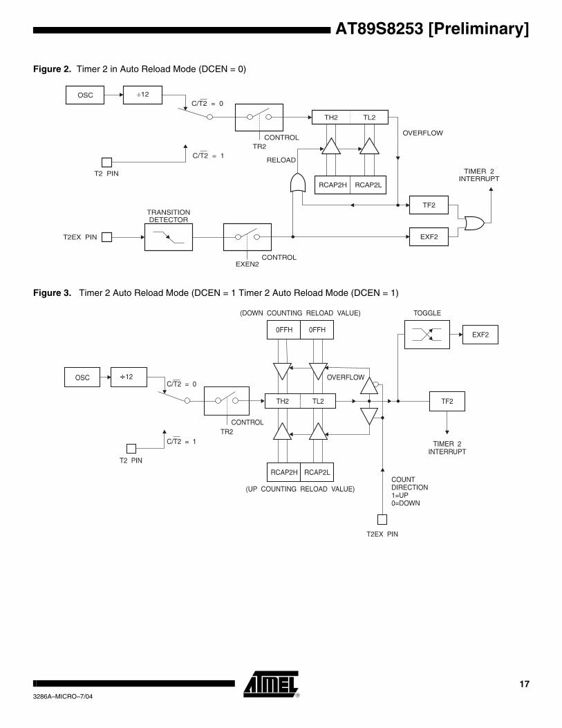
Auto-reload (Up or Down Counter)
Timer 2 can be programmed to count up or down when configured in its 16-bit auto-reloadmode. This feature is invoked by the DCEN (Down Counter Enable) bit located in the SFRT2MOD (see Table 9). Upon reset, the DCEN bit is set to 0 so that timer 2 will default to countup. When DCEN is set, Timer 2 can count up or down, depending on the value of the T2EXpin.
Figure 2 shows Timer 2 automatically counting up when DCEN = 0. In this mode, two optionsare selected by bit EXEN2 in T2CON. If EXEN2 = 0, Timer 2 counts up to 0FFFFH and thensets the TF2 bit upon overflow. The overflow also causes the timer registers to be reloadedwith the 16-bit value in RCAP2H and RCAP2L. The values in RCAP2H and RCAP2L arepreset by software. If EXEN2 = 1, a 16-bit reload can be triggered either by an overflow or by a1-to-0 transition at external input T2EX. This transition also sets the EXF2 bit. Both the TF2and EXF2 bits can generate an interrupt if enabled.
Setting the DCEN bit enables Timer 2 to count up or down, as shown in Figure 3. In this mode,the T2EX pin controls the direction of the count. A logic 1 at T2EX makes Timer 2 count up.The timer will overflow at 0FFFFH and set the TF2 bit. This overflow also causes the 16-bitvalue in RCAP2H and RCAP2L to be reloaded into the timer registers, TH2 and TL2,respectively.
A logic 0 at T2EX makes Timer 2 count down. The timer underflows when TH2 and TL2 equalthe values stored in RCAP2H and RCAP2L. The underflow sets the TF2 bit and causes0FFFFH to be reloaded into the timer registers.
The EXF2 bit toggles whenever Timer 2 overflows or underflows and can be used as a 17th bitof resolution. In this operating mode, EXF2 does not flag an interrupt.
Table 9. T2MOD – Timer 2 Mode Control Register
T2MOD Address = 0C9H Reset Value = XXXX XX00B
Not Bit Addressable
– – – – – – T2OE DCEN
Bit 7 6 5 4 3 2 1 0
Symbol Function
– Not implemented, reserved for future use.
T2OE Timer 2 Output Enable bit.
DCEN When set, this bit allows Timer 2 to be configured as an up/down counter.
16 AT89S8253 [Preliminary]3286A–MICRO–7/04
AT89S8253 [Preliminary]
Figure 2. Timer 2 in Auto Reload Mode (DCEN = 0)
Figure 3. Timer 2 Auto Reload Mode (DCEN = 1 Timer 2 Auto Reload Mode (DCEN = 1)
173286A–MICRO–7/04

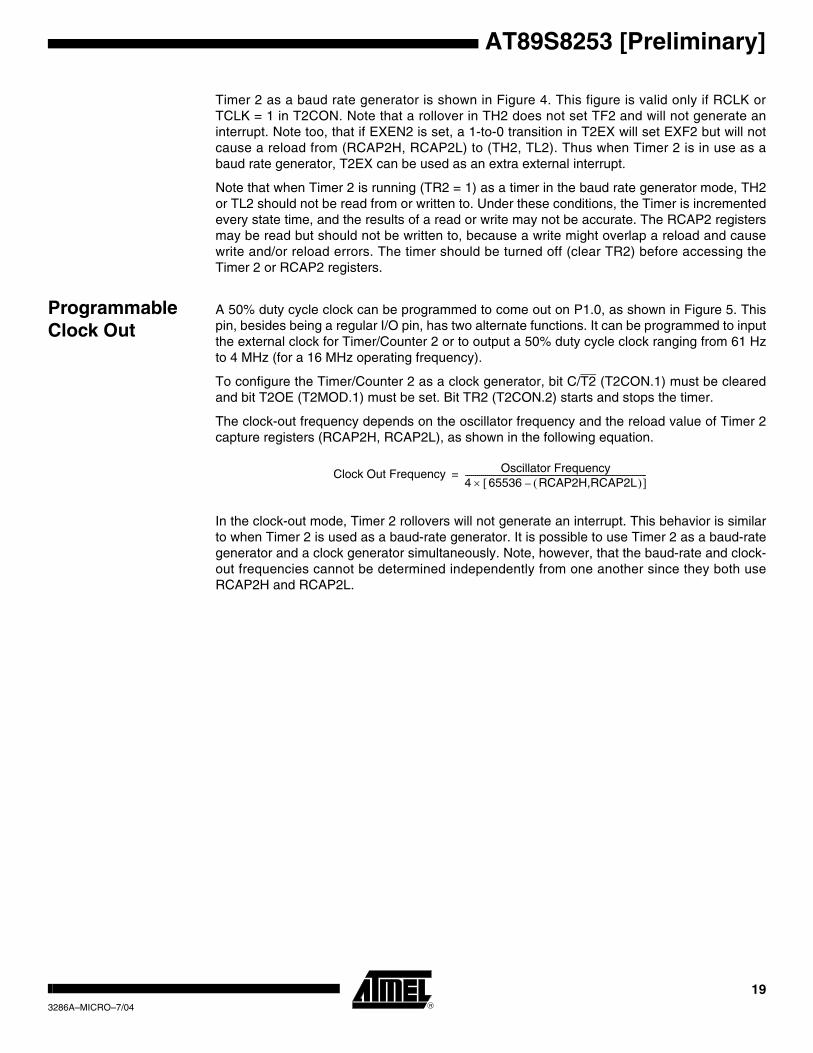
Figure 4. Timer 2 in Baud Rate Generator Mode
Baud Rate Generator
Timer 2 is selected as the baud rate generator by setting TCLK and/or RCLK in T2CON (Table8). Note that the baud rates for transmit and receive can be different if Timer 2 is used for thereceiver or transmitter and Timer 1 is used for the other function. Setting RCLK and/or TCLKputs Timer 2 into its baud rate generator mode, as shown in Figure 4.
The baud rate generator mode is similar to the auto-reload mode, in that a rollover in TH2causes the Timer 2 registers to be reloaded with the 16-bit value in registers RCAP2H andRCAP2L, which are preset by software.
The baud rates in Modes 1 and 3 are determined by Timer 2’s overflow rate according to thefollowing equation.
The Timer can be configured for either timer or counter operation. In most applications, it isconfigured for timer operation (CP/T2 = 0). The timer operation is different for Timer 2 when itis used as a baud rate generator. Normally, as a timer, it increments every machine cycle (at1/12 the oscillator frequency). As a baud rate generator, however, it increments every statetime (at 1/2 the oscillator frequency). The baud rate formula is given below.
where (RCAP2H, RCAP2L) is the content of RCAP2H and RCAP2L taken as a 16-bitunsigned integer.
OSC
SMOD1
RCLK
TCLK
RxCLOCK
TxCLOCK
T2EX PIN
T2 PIN
TR2CONTROL
"1"
"1"
"1"
"0"
"0"
"0"
TIMER 1 OVERFLOW
NOTE: OSC. FREQ. IS DIVIDED BY 2, NOT 12
TIMER 2INTERRUPT
2
2
16
16
RCAP2LRCAP2H
TH2 TL2
C/T2 = 0
C/T2 = 1
EXF2
CONTROL
TRANSITIONDETECTOR
EXEN2
÷
÷
÷
÷
Modes 1 and 3 Baud Rates Timer 2 Overflow Rate16
------------------------------------------------------------=
Modes 1 and 3Baud Rate
--------------------------------------- Oscillator Frequency32 65536 RCAP2H,RCAP2L( )–[ ]×----------------------------------------------------------------------------------------------=
18 AT89S8253 [Preliminary]3286A–MICRO–7/04
AT89S8253 [Preliminary]
Timer 2 as a baud rate generator is shown in Figure 4. This figure is valid only if RCLK orTCLK = 1 in T2CON. Note that a rollover in TH2 does not set TF2 and will not generate aninterrupt. Note too, that if EXEN2 is set, a 1-to-0 transition in T2EX will set EXF2 but will notcause a reload from (RCAP2H, RCAP2L) to (TH2, TL2). Thus when Timer 2 is in use as abaud rate generator, T2EX can be used as an extra external interrupt.
Note that when Timer 2 is running (TR2 = 1) as a timer in the baud rate generator mode, TH2or TL2 should not be read from or written to. Under these conditions, the Timer is incrementedevery state time, and the results of a read or write may not be accurate. The RCAP2 registersmay be read but should not be written to, because a write might overlap a reload and causewrite and/or reload errors. The timer should be turned off (clear TR2) before accessing theTimer 2 or RCAP2 registers.
Programmable Clock Out
A 50% duty cycle clock can be programmed to come out on P1.0, as shown in Figure 5. Thispin, besides being a regular I/O pin, has two alternate functions. It can be programmed to inputthe external clock for Timer/Counter 2 or to output a 50% duty cycle clock ranging from 61 Hzto 4 MHz (for a 16 MHz operating frequency).
To configure the Timer/Counter 2 as a clock generator, bit C/T2 (T2CON.1) must be clearedand bit T2OE (T2MOD.1) must be set. Bit TR2 (T2CON.2) starts and stops the timer.
The clock-out frequency depends on the oscillator frequency and the reload value of Timer 2capture registers (RCAP2H, RCAP2L), as shown in the following equation.
In the clock-out mode, Timer 2 rollovers will not generate an interrupt. This behavior is similarto when Timer 2 is used as a baud-rate generator. It is possible to use Timer 2 as a baud-rategenerator and a clock generator simultaneously. Note, however, that the baud-rate and clock-out frequencies cannot be determined independently from one another since they both useRCAP2H and RCAP2L.
Clock Out Frequency Oscillator Frequency4 65536 RCAP2H,RCAP2L( )–[ ]×-------------------------------------------------------------------------------------------=
193286A–MICRO–7/04

Figure 5. Timer 2 in Clock-out Mode
UART The UART in the AT89S8253 operates the same way as the UART in the AT89S51 andAT89S52. For more detailed information on the UART operation refer to the Atmel Web site(www.atmel.com). From the home page, select “Products,” then “Microcontrollers”, then“8051-Architecture,” then “Documentation”, and “Other Documents”. Open the Adobe Acrobatfile “AT89 Series Hardware Description.”
Enhanced UART In addition to all of its usual modes, the UART can perform framing error detection by lookingfor missing stop bits, and automatic address recognition. The UART also fully supports multi-processor communication as does the standard 80C51 UART.
When used for framing error detect, the UART looks for missing stop bits in the communica-tion. A missing bit will set the FE bit in the SCON register. The FE bit shares the SCON.7 bitwith SM0 and the function of SCON.7 is determined by PCON.6 (SMOD0). If SMOD0 is setthen SCON.7 functions as FE. SCON.7 functions as SM0 when SMOD0 is cleared. Whenused as FE, SCON.7 can only be cleared by software.
Automatic Address Recognition
Automatic Address Recognition is a feature which allows the UART to recognize certainaddresses in the serial bit stream by using hardware to make the comparisons. This featuresaves a great deal of software overhead by eliminating the need for the software to examineevery serial address which passes by the serial port. This feature is enabled by setting theSM2 bit in SCON. In the 9-bit UART modes, mode 2 and mode 3, the Receive Interrupt flag(RI) will be automatically set when the received byte contains either the “Given” address or the“Broadcast” address. The 9-bit mode requires that the 9th information bit is a 1 to indicate thatthe received information is an address and not data.
The 8-bit mode is called mode 1. In this mode the RI flag will be set if SM2 is enabled and theinformation received has a valid stop bit following the 8 address bits and the information iseither a Given or Broadcast address.
20 AT89S8253 [Preliminary]3286A–MICRO–7/04
AT89S8253 [Preliminary]
Mode 0 is the Shift Register mode and SM2 is ignored.
Using the Automatic Address Recognition feature allows a master to selectively communicatewith one or more slaves by invoking the given slave address or addresses. All of the slavesmay be contacted by using the Broadcast address. Two special Function Registers are usedto define the slave’s address, SADDR, and the address mask, SADEN. SADEN is used todefine which bits in the SADDR are to be used and which bits are “don’t care”. The SADENmask can be logically ANDed with the SADDR to create the “Given” address which the masterwill use for addressing each of the slaves. Use of the Given address allows multiple slaves tobe recognized while excluding others. The following examples will help to show the versatilityof this scheme:
Slave 0 SADDR = 1100 0000
SADEN = 1111 1101
Given = 1100 00X0
Slave 1 SADDR = 1100 0000
SADEN = 1111 1110
Given = 1100 000X
In the previous example SADDR is the same and the SADEN data is used to differentiatebetween the two slaves. Slave 0 requires a 0 in bit 0 and it ignores bit 1. Slave 1 requires a 0in bit 1 and bit 0 is ignored. A unique address for slave 0 would be 1100 0010 since slave 1requires a 0 in bit 1. A unique address for slave 1 would be 1100 0001 since a 1 in bit 0 willexclude slave 0. Both slaves can be selected at the same time by an address which has bit 0= 0 (for slave 0) and bit 1 = 0 (for slave 1). Thus, both could be addressed with 1100 0000.
In a more complex system the following could be used to select slaves 1 and 2 while excludingslave 0:
Slave 0 SADDR = 1100 0000
SADEN = 1111 1001
Given = 1100 0XX0
Slave 1 SADDR = 1110 0000
SADEN = 1111 1010
Given = 1110 0X0X
Slave 2 SADDR = 1110 0000
SADEN = 1111 1100
Given = 1110 00XX
In the above example the differentiation among the 3 slaves is in the lower 3 address bits.Slave 0 requires that bit 0 = 0 and it can be uniquely addressed by 1110 0110. Slave 1requires that bit 1 = 0 and it can be uniquely addressed by 1110 and 0101. Slave 2 requiresthat bit 2 = 0 and its unique address is 1110 0011. To select Slaves 0 and 1 and exclude Slave2, use address 1110 0100, since it is necessary to make bit 2 = 1 to exclude slave 2.
213286A–MICRO–7/04

The Broadcast Address for each slave is created by taking the logical OR of SADDR andSADEN. Zeros in this result are trended as don’t-cares. In most cases, interpreting the don’t-cares as ones, the broadcast address will be FF hexadecimal.
Upon reset SADDR (SFR address 0A9H) and SADEN (SFR address 0B9H) are leaded with0s. This produces a given address of all “don’t cares” as well as a Broadcast address of all“don’t cares”. This effectively disables the Automatic Addressing mode and allows the micro-controller to use standard 80C51-type UART drivers which do not make use of this feature.
Notes: 1. SMOD is located at PCON.7.2. fosc = oscillator frequency.
Table 10. SCON – Serial Port Control Register
SCON Address = 98H Reset Value = 0000 0000B
Bit Addressable
SM0/FE SM1 SM2 REN TB8 RB8 T1 RI
Bit 7 6 5 4 3 2 1 0
(SMOD = 0/1)(1)
Symbol Function
FE Framing error bit. This bit is set by the receiver when an invalid stop bit is detected. The FE bit is not cleared by valid frames but should be cleared by software. The SMOD0 bit must be set to enable access to the FE bit. FE will be set regardless of the state of SMOD.
SM0 Serial Port Mode Bit 0, (SMOD must = 0 to access bit SM0)
SM1 Serial Port Mode Bit 1
SM2 Enables the Automatic Address Recognition feature in modes 2 or 3. If SM2 = 1 then Rl will not be set unless the received 9th data bit (RB8) is 1, indicating an address, and the received byte is a Given or Broadcast Address. In mode 1, if SM2 = 1 then Rl will not be activated unless a valid stop bit was received, and the received byte is a Given or Broadcast Address. In Mode 0, SM2 should be 0.
REN Enables serial reception. Set by software to enable reception. Clear by software to disable reception.
TB8 The 9th data bit that will be transmitted in modes 2 and 3. Set or clear by software as desired.
RB8 In modes 2 and 3, the 9th data bit that was received. In mode 1, if SM2 = 0, RB8 is the stop bit that wasreceived. In mode 0, RB8 is not used.
TI Transmit interrupt flag. Set by hardware at the end of the 8th bit time in mode 0, or at the beginning of thestop bit in the other modes, in any serial transmission. Must be cleared by software.
RI Receive interrupt flag. Set by hardware at the end of the 8th bit time in mode 0, or halfway through the stopbit time in the other modes, in any serial reception (except see SM2). Must be cleared by software.
SM0 SM1 Mode Description Baud Rate(2)
0 0 0 shift register fosc/12
0 1 1 8-bit UART variable
1 0 2 9-bit UART fosc/64 or fosc/32
1 1 3 9-bit UART variable
22 AT89S8253 [Preliminary]3286A–MICRO–7/04

AT89S8253 [Preliminary]
Serial Peripheral Interface
The serial peripheral interface (SPI) allows high-speed synchronous data transfer between theAT89S8253 and peripheral devices or between multiple AT89S8253 devices. The AT89S8253SPI features include the following:
• Full-Duplex, 3-Wire Synchronous Data Transfer
• Master or Slave Operation
• Maximum Bit Frequency = f/4 (f/2 if in x2 Clock Mode)
• LSB First or MSB First Data Transfer
• Four Programmable Bit Rates in Master Mode
• End of Transmission Interrupt Flag
• Write Collision Flag Protection
• Double-Buffered Receive
• Double-Buffered Transmit (Enhanced Mode only)
• Wakeup from Idle Mode (Slave Mode only)
The interconnection between master and slave CPUs with SPI is shown in Figure 6. The fourpins in the interface are Master-In/Slave-Out (MISO), Master-Out/Slave-In (MOSI), Shift Clock(SCK), and Slave Select (SS). The SCK pin is the clock output in master mode, but is the clockinput in slave mode. The MSTR bit in SPCR determines the directions of MISO and MOSI.Also notice that MOSI connects to MOSI and MISO to MISO. In master mode, SS/P1.4 isignored and may be used as a general-purpose input or output. In slave mode, SS must bedriven low to select an individual device as a slave. When SS is driven high, the slave’s SPIport is deactivated and the MOSI/P1.5 pin can be used as a general-purpose input.
Figure 6. SPI Master-Slave Interconnection
8-BIT SHIFT REGISTER
MASTER
CLOCK GENERATORSPI
MISO
8-BIT SHIFT REGISTER
SLAVEMISO
MOSI MOSI
SCK SCK
SS SS
VCC
MSB LSB MSB LSB
233286A–MICRO–7/04

Figure 7. SPI Block Diagram
The SPI has two modes of operation: normal (non-buffered write) and enhanced (bufferedwrite). In normal mode, writing to the SPI data register (SPDR) of the master CPU starts theSPI clock generator and the data written shifts out of the MOSI pin and into the MOSI pin ofthe slave CPU. Transmission may start after an initial delay while the clock generator waits forthe next full bit slot of the specified baud rate. After shifting one byte, the SPI clock generatorstops, setting the end of transmission flag (SPIF) and transferring the received byte to the readbuffer (SPDR). If both the SPI interrupt enable bit (SPIE) and the serial port interrupt enable bit(ES) are set, an interrupt is requested. Note that SPDR refers to either the write data buffer orthe read data buffer, depending on whether the access is a write or read. In normal mode,because the write buffer is transparent (and a write access to SPDR will be directed to the shiftbuffer), any attempt to write to SPDR while a transmission is in progress will result in a writecollision with WCOL set. However, the transmission will still complete normally, but the newbyte will be ignored and a new write access to SPDR will be necessary.
Enhanced mode is similar to normal mode except that the write buffer holds the next byte tobe transmitted. Writing to SPDR loads the write buffer and sets WCOL to signify that the bufferis full and any further writes will overwrite the buffer. WCOL is cleared by hardware when thebuffered byte is loaded into the shift register and transmission begins. If the master SPI is cur-rently idle, i.e. if this is the first byte, then after loading SPDR, transmission of the byte startsand WCOL is cleared immediately. While this byte is transmitting, the next byte may be writtento SPDR. The Load Enable flag (LDEN) in SPSR can be used to determine when transmissionhas started. LDEN is asserted during the first four bit slots of a SPI transfer. The master CPUshould first check that LDEN is set and that WCOL is cleared before loading the next byte. Inenhanced mode, if WCOL is set when a transfer completes, i.e. the next byte is available, thenthe SPI immediately loads the buffered byte into the shift register, resets WCOL, and contin-ues transmission without stopping and restarting the clock generator. As long as the CPU cankeep the write buffer full in this manner, multiple bytes may be transferred with minimal latencybetween bytes.
OSCILLATOR
8/16-BIT SHIFT REGISTER
READ DATA BUFFER
PIN
CO
NT
RO
L LO
GIC
SPI CONTROL
SPI STATUS REGISTER
SPI INTERRUPTREQUEST
INTERNALDATA BUS
SELECTSPI CLOCK (MASTER)
DIVIDER÷4÷16÷64÷128
SPI CONTROL REGISTER
8
8
8
SP
IF
WC
OL
SP
R1
MSTR
SP
IE
CLOCKLOGIC
CLOCK
MSB
S
M
SP
E
DO
RD
MS
TR
CP
OL
CP
HA
SP
R1
SP
R0
MS
TR
SP
E
DO
RD
LSB
S
MM
S
MISOP1.6
MOSIP1.5
SCK1.7
SSP1.4
SP
R0
SPE
WRITE DATA BUFFER
24 AT89S8253 [Preliminary]3286A–MICRO–7/04
AT89S8253 [Preliminary]
Notes: 1. Set up the clock mode before enabling the SPI: set all bits needed in SPCR except the SPE bit, then set SPE.2. Enable the master SPI prior to the slave device.3. Slave echoes master on next Tx if not loaded with new data.
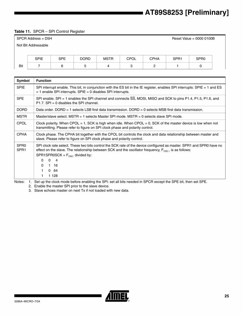
Table 11. SPCR – SPI Control Register
SPCR Address = D5H Reset Value = 0000 0100B
Not Bit Addressable
SPIE SPE DORD MSTR CPOL CPHA SPR1 SPR0
Bit 7 6 5 4 3 2 1 0
Symbol Function
SPIE SPI interrupt enable. This bit, in conjunction with the ES bit in the IE register, enables SPI interrupts: SPIE = 1 and ES = 1 enable SPI interrupts. SPIE = 0 disables SPI interrupts.
SPE SPI enable. SPI = 1 enables the SPI channel and connects SS, MOSI, MISO and SCK to pins P1.4, P1.5, P1.6, and P1.7. SPI = 0 disables the SPI channel.
DORD Data order. DORD = 1 selects LSB first data transmission. DORD = 0 selects MSB first data transmission.
MSTR Master/slave select. MSTR = 1 selects Master SPI mode. MSTR = 0 selects slave SPI mode.
CPOL Clock polarity. When CPOL = 1, SCK is high when idle. When CPOL = 0, SCK of the master device is low when not transmitting. Please refer to figure on SPI clock phase and polarity control.
CPHA Clock phase. The CPHA bit together with the CPOL bit controls the clock and data relationship between master and slave. Please refer to figure on SPI clock phase and polarity control.
SPR0SPR1
SPI clock rate select. These two bits control the SCK rate of the device configured as master. SPR1 and SPR0 have no effect on the slave. The relationship between SCK and the oscillator frequency, FOSC., is as follows:
SPR1SPR0SCK = FOSC. divided by:
0 0 40 1 16
1 0 64
1 1 128
253286A–MICRO–7/04

Table 12. SPSR – SPI Status Register
SPSR Address = AAH Reset Value = 000X XX00B
Not Bit Addressable
SPIF WCOL LDEN – – – DISSO ENH
Bit 7 6 5 4 3 2 1 0
Symbol Function
SPIF SP interrupt flag. When a serial transfer is complete, the SPIF bit is set and an interrupt is generated if SPIE = 1 and ES = 1. The SPIF bit is cleared by reading the SPI status register with SPIF and WCOL bits set, and then reading/writing the SPI data register.
WCOL When ENH = 0: Write collision flag. The WCOL bit is set if the SPI data register is written during a data transfer. During data transfer, the result of reading the SPDR register may be incorrect, and writing to it has no effect. The WCOL bit (and the SPIF bit) are cleared by reading the SPI status register with SPIF and WCOL set, and then reading/writing the SPI data register.
When ENH = 1: WCOL works in Enhanced mode as Tx Buffer Full. Writing during WCOL = 1 in enhanced mode will overwrite the waiting data already present in the Tx Buffer. In this mode, WCOL is no longer reset by the SPIF reset but is reset when the write buffer has been unloaded into the serial shift register.
LDEN Load enable for the Tx buffer in enhanced SPI mode.
When ENH is set, it is safe to load the Tx Buffer while LDEN = 1 and WCOL = 0. LDEN is high during bits 0 - 3 and is low during bits 4 - 7 of the SPI serial byte transmission time frame.
DISSO Disable slave output bit.
When set, this bit causes the MISO pin to be tri-stated so more than one slave device can share the same interface with a single master. Normally, the first byte in a transmission could be the slave address and only the selected slave should clear its DISSO bit.
ENH Enhanced SPI mode select bit. When ENH = 0, SPI is in normal mode, i.e. without write double buffering.
When ENH = 1, SPI is in enhanced mode with write double buffering. The Tx buffer shares the same address with the SPDR register.
Table 13. SPDR – SPI Data Register
SPDR Address = 86H Reset Value = 00H (after cold reset) unchanged (after warm reset)
Not Bit Addressable
SPD7 SPD6 SPD5 SPD4 SPD3 SPD2 SPD1 SPD0
Bit 7 6 5 4 3 2 1 0
26 AT89S8253 [Preliminary]3286A–MICRO–7/04
AT89S8253 [Preliminary]
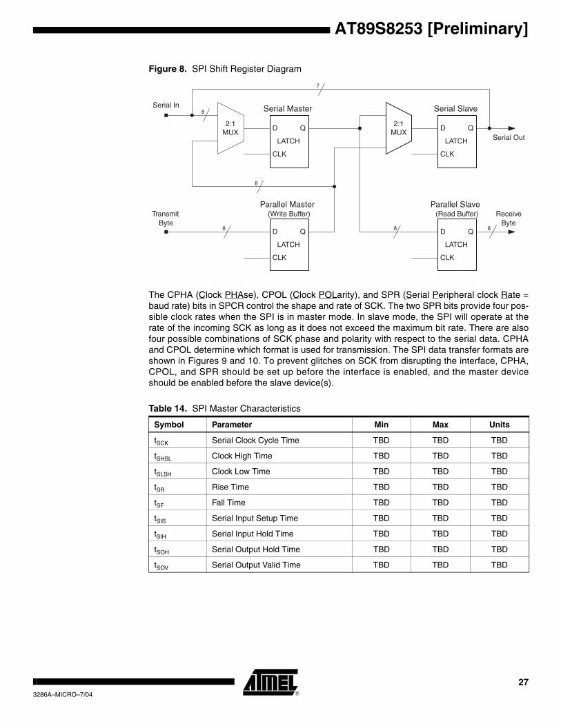
Figure 8. SPI Shift Register Diagram
The CPHA (Clock PHAse), CPOL (Clock POLarity), and SPR (Serial Peripheral clock Rate =baud rate) bits in SPCR control the shape and rate of SCK. The two SPR bits provide four pos-sible clock rates when the SPI is in master mode. In slave mode, the SPI will operate at therate of the incoming SCK as long as it does not exceed the maximum bit rate. There are alsofour possible combinations of SCK phase and polarity with respect to the serial data. CPHAand CPOL determine which format is used for transmission. The SPI data transfer formats areshown in Figures 9 and 10. To prevent glitches on SCK from disrupting the interface, CPHA,CPOL, and SPR should be set up before the interface is enabled, and the master deviceshould be enabled before the slave device(s).
Table 14. SPI Master Characteristics
Symbol Parameter Min Max Units
tSCK Serial Clock Cycle Time TBD TBD TBD
tSHSL Clock High Time TBD TBD TBD
tSLSH Clock Low Time TBD TBD TBD
tSR Rise Time TBD TBD TBD
tSF Fall Time TBD TBD TBD
tSIS Serial Input Setup Time TBD TBD TBD
tSIH Serial Input Hold Time TBD TBD TBD
tSOH Serial Output Hold Time TBD TBD TBD
tSOV Serial Output Valid Time TBD TBD TBD
2:1MUX
2:1MUX
Serial Master Serial Slave
LATCH
D Q
CLK
LATCH
D Q
CLK
LATCH
D Q
CLK
LATCH
D Q
CLK
Parallel Slave(Read Buffer)
Parallel Master(Write Buffer)
Serial Out
ReceiveByte
Serial In
TransmitByte
8 8
8
8
7
8
273286A–MICRO–7/04
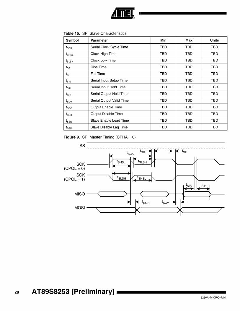
Figure 9. SPI Master Timing (CPHA = 0)
Table 15. SPI Slave Characteristics
Symbol Parameter Min Max Units
tSCK Serial Clock Cycle Time TBD TBD TBD
tSHSL Clock High Time TBD TBD TBD
tSLSH Clock Low Time TBD TBD TBD
tSR Rise Time TBD TBD TBD
tSF Fall Time TBD TBD TBD
tSIS Serial Input Setup Time TBD TBD TBD
tSIH Serial Input Hold Time TBD TBD TBD
tSOH Serial Output Hold Time TBD TBD TBD
tSOV Serial Output Valid Time TBD TBD TBD
tSOE Output Enable Time TBD TBD TBD
tSOX Output Disable Time TBD TBD TBD
tSSE Slave Enable Lead Time TBD TBD TBD
tSSD Slave Disable Lag Time TBD TBD TBD
SS
SCK(CPOL = 0)
SCK(CPOL = 1)
MISO
MOSI
tSRtSCK
tSLSH
tSLSH
tSHSL
tSHSL
tSOH
tSF
tSIS tSIH
tSOV
28 AT89S8253 [Preliminary]3286A–MICRO–7/04
AT89S8253 [Preliminary]
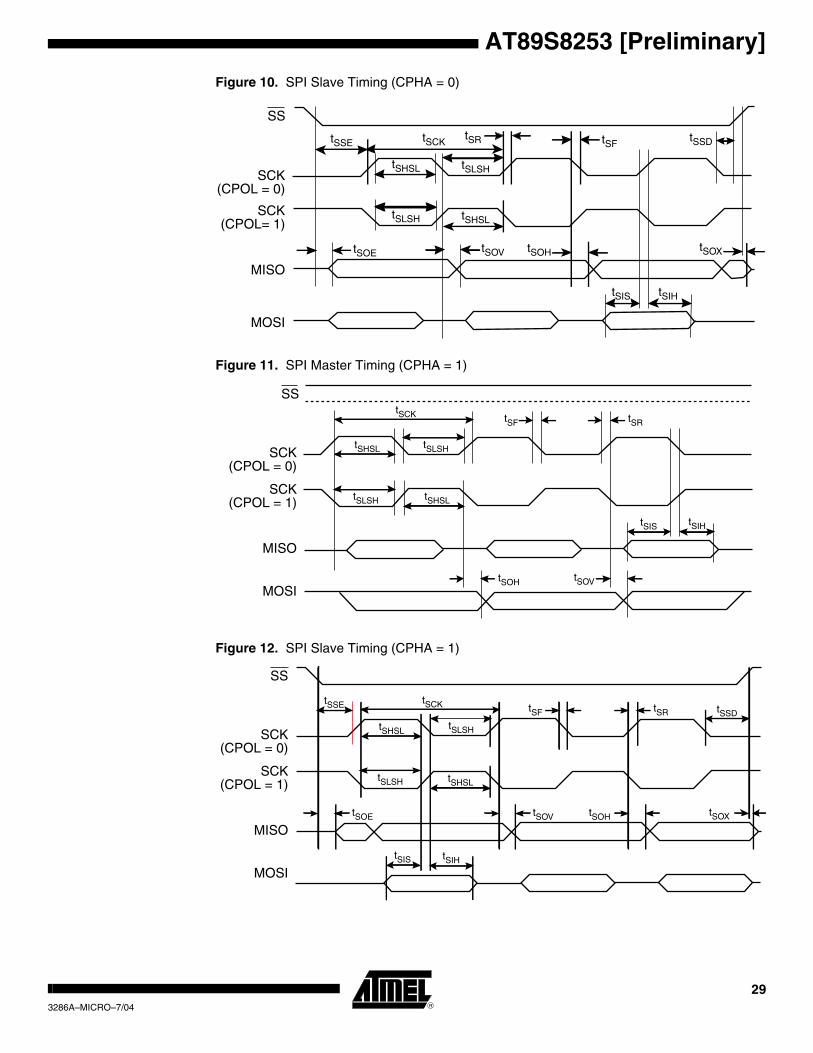
Figure 10. SPI Slave Timing (CPHA = 0)
Figure 11. SPI Master Timing (CPHA = 1)
Figure 12. SPI Slave Timing (CPHA = 1)
tSRtSSE
tSLSH
tSHSL
tSOV
tSF
tSOX
tSSDtSCK
tSLSH
tSHSL
tSOE tSOH
tSIHtSIS
SS
SCK(CPOL = 0)
SCK(CPOL= 1)
MISO
MOSI
tSHSL tSLSH
tSHSLtSLSH
tSCK
tSOH
tSF tSR
tSIS
tSOV
tSIH
SS
SCK(CPOL = 0)
SCK(CPOL = 1)
MISO
MOSI
SS
SCK(CPOL = 0)
SCK(CPOL = 1)
MISO
MOSI
tSCKtSSE
tSHSL
tSHSLtSLSH
tSLSH
tSSD
tSIHtSIS
tSOE tSOV tSOH tSOX
tSF tSR
293286A–MICRO–7/04

Figure 13. SPI Transfer Format with CPHA = 0
Note: *Not defined but normally MSB of character just received
Figure 14. SPI Transfer Format with CPHA = 1
Note: *Not defined but normally LSB of previously transmitted character
Interrupts The AT89S8253 has a total of six interrupt vectors: two external interrupts (INT0 and INT1),three timer interrupts (Timers 0, 1, and 2), and the serial port interrupt. These interrupts are allshown in Figure 15.
Each of these interrupt sources can be individually enabled or disabled by setting or clearing abit in Special Function Register IE. IE also contains a global disable bit, EA, which disables allinterrupts at once.
Note that Table 16 shows that bit position IE.6 is unimplemented. User software should notwrite a 1 to this bit position, since it may be used in future AT89 products.
Timer 2 interrupt is generated by the logical OR of bits TF2 and EXF2 in register T2CON. Nei-ther of these flags is cleared by hardware when the service routine is vectored to. In fact, theservice routine may have to determine whether it was TF2 or EXF2 that generated the inter-rupt, and that bit will have to be cleared in software.
The serial interrupt is the logical OR of bits RI and TI in register SCON and also bit SPIF inSPSR (if SPIE in SPCR is set). None of these flags is cleared by hardware when the serviceroutine is vectored to. The service routine may have to determine whether the UART or SPIgenerated the interrupt.
The Timer 0 and Timer 1 flags, TF0 and TF1, are set at S5P2 of the cycle in which the timersoverflow. The values are then polled by the circuitry in the next cycle. However, the Timer 2flag, TF2, is set at S2P2 and is polled in the same cycle in which the timer overflows.
MSB 6 5 4 3 2 1 LSB
1 2 3 4 5 6 7 8
MSB* 6 5 4 3 2 1 LSB
SCK CYCLE #(FOR REFERENCE)
SCK (CPOL = 0)
SCK (CPOL = 1)
MOSI(FROM MASTER)
MISO(FROM SLAVE)
SS (TO SLAVE)
30 AT89S8253 [Preliminary]3286A–MICRO–7/04
AT89S8253 [Preliminary]
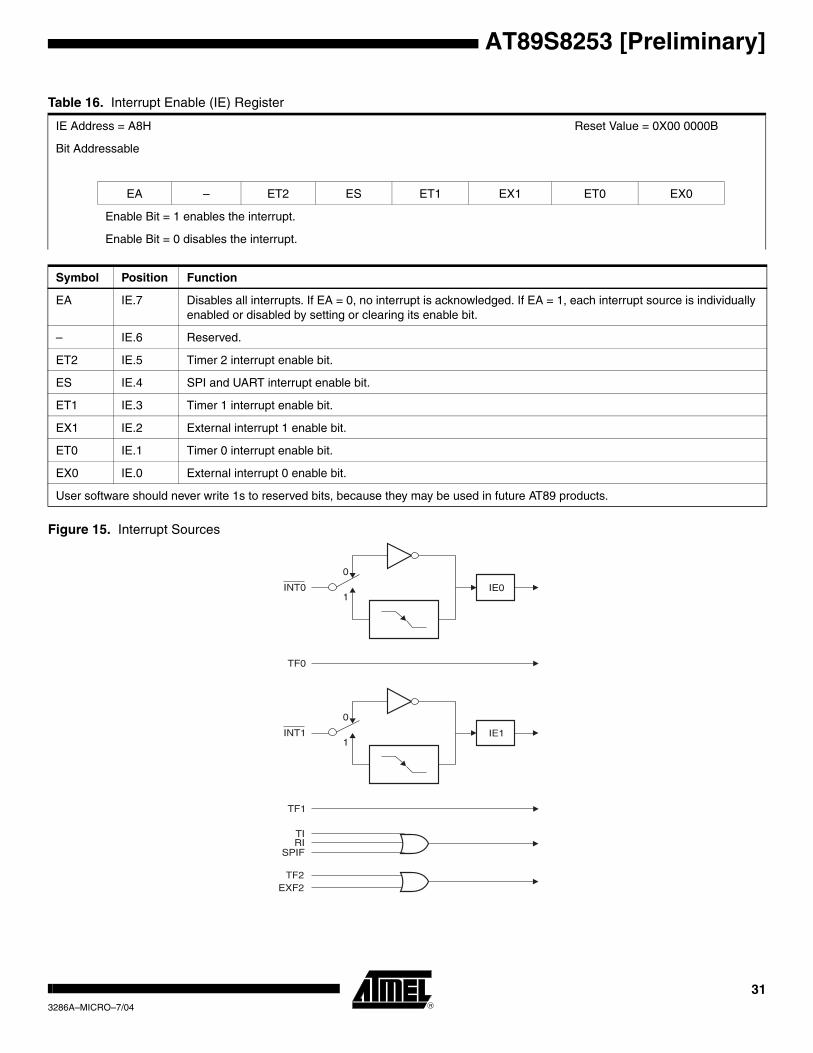
Figure 15. Interrupt Sources
Table 16. Interrupt Enable (IE) Register
IE Address = A8H Reset Value = 0X00 0000B
Bit Addressable
EA – ET2 ES ET1 EX1 ET0 EX0
Enable Bit = 1 enables the interrupt.
Enable Bit = 0 disables the interrupt.
Symbol Position Function
EA IE.7 Disables all interrupts. If EA = 0, no interrupt is acknowledged. If EA = 1, each interrupt source is individually enabled or disabled by setting or clearing its enable bit.
– IE.6 Reserved.
ET2 IE.5 Timer 2 interrupt enable bit.
ES IE.4 SPI and UART interrupt enable bit.
ET1 IE.3 Timer 1 interrupt enable bit.
EX1 IE.2 External interrupt 1 enable bit.
ET0 IE.1 Timer 0 interrupt enable bit.
EX0 IE.0 External interrupt 0 enable bit.
User software should never write 1s to reserved bits, because they may be used in future AT89 products.
313286A–MICRO–7/04
Oscillator Characteristics
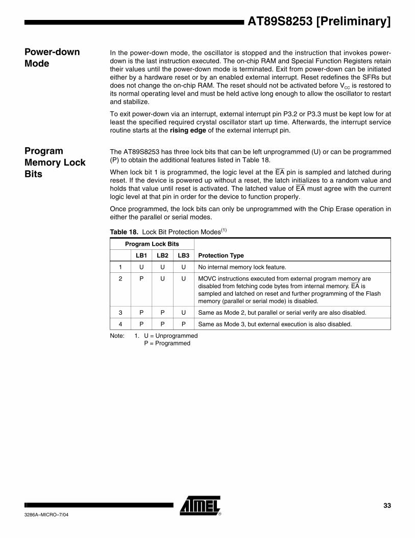
XTAL1 and XTAL2 are the input and output, respectively, of an inverting amplifier that can beconfigured for use as an on-chip oscillator, as shown in Figure 16. Either a quartz crystal orceramic resonator may be used. To drive the device from an external clock source, XTAL2should be left unconnected while XTAL1 is driven, as shown in Figure 17. There are norequirements on the duty cycle of the external clock signal, since the input to the internal clock-ing circuitry is through a divide-by-two flip-flop, but minimum and maximum voltage high andlow time specifications must be observed.
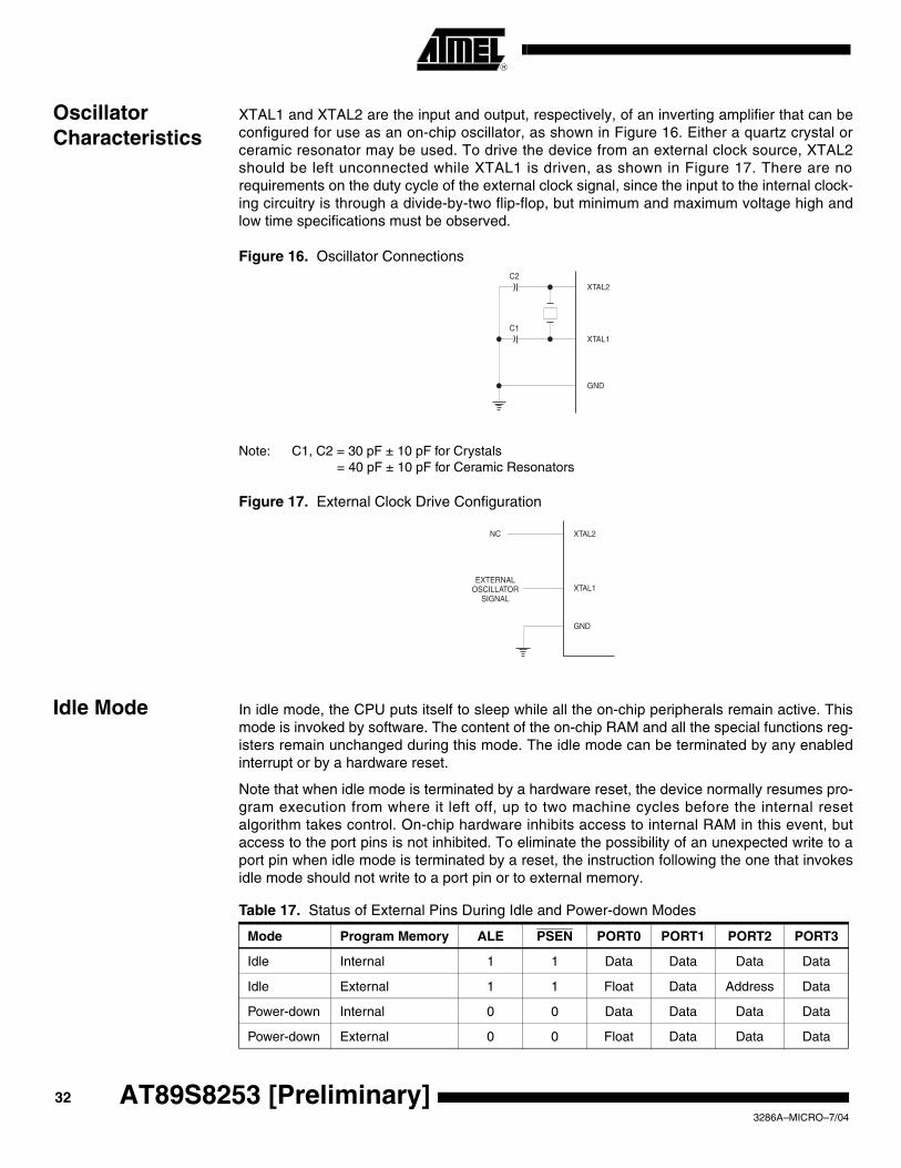
Figure 16. Oscillator Connections
Note: C1, C2 = 30 pF ± 10 pF for Crystals= 40 pF ± 10 pF for Ceramic Resonators
Figure 17. External Clock Drive Configuration
Idle Mode In idle mode, the CPU puts itself to sleep while all the on-chip peripherals remain active. Thismode is invoked by software. The content of the on-chip RAM and all the special functions reg-isters remain unchanged during this mode. The idle mode can be terminated by any enabledinterrupt or by a hardware reset.
Note that when idle mode is terminated by a hardware reset, the device normally resumes pro-gram execution from where it left off, up to two machine cycles before the internal resetalgorithm takes control. On-chip hardware inhibits access to internal RAM in this event, butaccess to the port pins is not inhibited. To eliminate the possibility of an unexpected write to aport pin when idle mode is terminated by a reset, the instruction following the one that invokesidle mode should not write to a port pin or to external memory.
Table 17. Status of External Pins During Idle and Power-down Modes
Mode Program Memory ALE PSEN PORT0 PORT1 PORT2 PORT3
Idle Internal 1 1 Data Data Data Data
Idle External 1 1 Float Data Address Data
Power-down Internal 0 0 Data Data Data Data
Power-down External 0 0 Float Data Data Data
32 AT89S8253 [Preliminary]3286A–MICRO–7/04
AT89S8253 [Preliminary]
Power-down Mode
In the power-down mode, the oscillator is stopped and the instruction that invokes power-down is the last instruction executed. The on-chip RAM and Special Function Registers retaintheir values until the power-down mode is terminated. Exit from power-down can be initiatedeither by a hardware reset or by an enabled external interrupt. Reset redefines the SFRs butdoes not change the on-chip RAM. The reset should not be activated before VCC is restored toits normal operating level and must be held active long enough to allow the oscillator to restartand stabilize.
To exit power-down via an interrupt, external interrupt pin P3.2 or P3.3 must be kept low for atleast the specified required crystal oscillator start up time. Afterwards, the interrupt serviceroutine starts at the rising edge of the external interrupt pin.
Program Memory Lock Bits
The AT89S8253 has three lock bits that can be left unprogrammed (U) or can be programmed(P) to obtain the additional features listed in Table 18.
When lock bit 1 is programmed, the logic level at the EA pin is sampled and latched duringreset. If the device is powered up without a reset, the latch initializes to a random value andholds that value until reset is activated. The latched value of EA must agree with the currentlogic level at that pin in order for the device to function properly.
Once programmed, the lock bits can only be unprogrammed with the Chip Erase operation ineither the parallel or serial modes.
Note: 1. U = UnprogrammedP = Programmed
Table 18. Lock Bit Protection Modes(1)
Program Lock Bits
Protection TypeLB1 LB2 LB3
1 U U U No internal memory lock feature.
2 P U U MOVC instructions executed from external program memory are disabled from fetching code bytes from internal memory. EA is sampled and latched on reset and further programming of the Flash memory (parallel or serial mode) is disabled.
3 P P U Same as Mode 2, but parallel or serial verify are also disabled.
4 P P P Same as Mode 3, but external execution is also disabled.
333286A–MICRO–7/04

Programming the Flash and EEPROM
Atmel’s AT89S8253 Flash microcontroller offers 12K bytes of In-System reprogrammableFlash code memory and 2K bytes of EEPROM data memory.
The AT89S8253 is normally shipped with the on-chip Flash code and EEPROM data memoryarrays in the erased state (i.e. contents = FFH) and ready to be programmed. This device sup-ports a parallel programming mode and a serial programming mode. The serial programmingmode provides a convenient way to reprogram the AT89S8253 inside the user’s system. Theparallel programming mode is compatible with conventional third-party Flash or EPROMprogrammers.
The code and data memory arrays are mapped via separate address spaces in the paralleland serial programming modes: 0000H to 2FFFH for code memory and 000H to 7FFH for datamemory.
The code and data memory arrays in the AT89S8253 are programmed byte-by-byte or bypage in either programming mode. To reprogram any non-blank byte in the parallel or serialmode, the user needs to invoke the Chip Erase operation first to erase both arrays.
Parallel Programming Algorithm: To program and verify the AT89S8253 in the parallel pro-gramming mode, the following sequence is recommended (see Figure 21):
1. Power-up sequence:
Apply power between VCC and GND pins.
Set RST pin to “H”.
Apply a 3 MHz to 24 MHz clock to XTAL1 pin and wait for at least 10 ms.
2. Set PSEN pin to “L”
ALE pin to “H”
EA pin to “H” and all other pins to “H”.
3. Raise EA/VPP to 12V to enable Flash programming, erase or verification. Enable the P3.0 pull-up (10 KΩ typical) for RDY/BSY operation.
4. Apply the appropriate combination of “H” or “L” logic levels to pins P3.3, P3.4, P3.5, P3.6, P3.7 to select one of the programming operations shown in the Flash Program-ming Modes table.
5. Apply the desired byte address to pins P1.0 to P1.7 and P2.0 to P2.5.
Apply data to pins P0.0 to P0.7 for write code operation.
6. Pulse ALE/PROG once to load a byte in the code memory array, the data memory array, or the lock bits.
7. Repeat steps 5 and 6, changing the address and data for up to 64 bytes in the code memory page or 32 bytes in the data memory (EEPROM) page. When loading a page with individual bytes, the interval between consecutive byte loads should be no longer than 150 µs. Otherwise the device internally times out and assumes that the page load sequence is completed, rejecting any further loads before the page programming sequence has finished. This timing restriction also applies to Page Write of the 64-byte User Row.
8. After the last byte of the current page has been loaded, wait for 5 ms or monitor the RDY/BUSY pin until it transitions high. The page write cycle is self-timed and typically takes less than 5 ms.
9. To verify the last byte of the page just programmed, bring pin P3.4 to “L” and read the programmed data at pins P0.0 to P0.7.
10. Repeat steps 4 through 7 changing the address and data for the entire array or until the end of the object file is reached.
34 AT89S8253 [Preliminary]3286A–MICRO–7/04

AT89S8253 [Preliminary]
11. Power-off sequence:
Tri-state the address and data inputs.
Disable the P3.0 pullup used for RDY/BUSY operation.
Set XTAL1 to “L”.
Set RST and EA pins to “L”.
Turn VCC power off.
Data Polling: The AT89S8253 features DATA Polling to indicate the end of a byte write cycle.During a write cycle in the parallel or serial programming mode, an attempted read of the lastloaded byte will result in the complement of the written datum on P0.7 (parallel mode), and onthe MSB of the serial output byte on MISO (serial mode). Once the write cycle has been com-pleted, true data are valid on all outputs, and the next cycle may begin. DATA Polling maybegin any time after a write cycle has been initiated.
Ready/Busy: The progress of byte programming in the parallel programming mode can alsobe monitored by the RDY/BSY output signal. Pin P3.0 is pulled Low after ALE goes High dur-ing programming to indicate BUSY. P3.0 is pulled High again when programming is done toindicate READY. P3.0 needs an external pullup (typical 10 KΩ) when functioning as RDY/BSY.
Program Verify: If lock bits LB1 and LB2 have not been programmed, the programmed Codeor Data byte can be read back via the address and data lines for verification. The state of thelock bits can also be verified directly in the parallel and serial programming modes.
Chip Erase: Both Flash and EEPROM arrays are erased electrically at the same time. In theparallel programming mode, Chip Erase is initiated by using the proper combination of controlsignals. The code and data arrays are written with all “1”s during the Chip Erase operation.The User Row will also be erased if the UsrRowProEn fuse (Fuse3) = 0 (enabled state).
In the serial programming mode, a chip erase operation is initiated by issuing the Chip Eraseinstruction. In this mode, Chip Erase is self-timed and also takes about 8 ms.
During Chip Erase, a serial read from any address location will return 00H at the data outputs.
Serial Programming Fuse: A programmable fuse is available to disable Serial Programmingif the user needs maximum system security. The Serial Programming Fuse can beenabled/disabled in both the Parallel/Serial Programming Modes.
The AT89S8253 is shipped with the Serial Programming Mode enabled.
Reading the Signature Bytes: The signature bytes are read by the same procedure as a nor-mal verification of locations 030H and 031H, except that P3.6 and P3.7 must be pulled to alogic low. The values returned are as follows:
(030H) = 1EH indicates manufactured by Atmel(031H) = 73H indicates AT89S8253
Programming Interface
Every code byte in the Flash and EEPROM arrays can be written, and the entire array can beerased, by using the appropriate combination of control signals. The write operation cycle isself-timed and once initiated, will automatically time itself to completion.
Most worldwide major programming vendors offer support for the Atmel AT89 microcontrollerseries. Please contact your local programming vendor for the appropriate software revision.
353286A–MICRO–7/04
Serial Downloading
Both the code and data memory arrays can be programmed using the serial SPI bus whileRST is pulled to VCC. The serial interface consists of pins SCK, MOSI (input) and MISO (out-put). After RST is set high, the Programming Enable instruction must be executed first beforeother operations can be executed.
The Chip Erase operation turns the content of every memory location in both the Code andData arrays into FFH.
The code and data memory arrays have separate address spaces:
0000H to 2FFFH for code memory and 000H to 7FFH for data memory.
Either an external system clock is supplied at pin XTAL1 or a crystal needs to be connectedacross pins XTAL1 and XTAL2. The maximum serial clock (SCK) frequency should be lessthan 1/16 of the crystal frequency. With a 24 MHz oscillator clock, the maximum SCK fre-quency is 1.5 MHz.
Serial Programming Algorithm
To program and verify the AT89S8253 in the serial programming mode, the followingsequence is recommended:
1. Power-up sequence:
Apply power between VCC and GND pins.
Set RST pin to “H”.
If a crystal is not connected across pins XTAL1 and XTAL2, apply a 3 MHz to 24 MHzclock to XTAL1 pin and wait for at least 10 ms with RST pin high and P1.7 (SCK) low.
2. Enable serial programming by sending the Programming Enable serial instruction to pin MOSI/P1.5. The frequency of the shift clock supplied at pin SCK/P1.7 needs to be less than the CPU clock at XTAL1 divided by 16.
3. The code or data array is programmed one byte or one page at a time by supplying the address and data together with the appropriate Write instruction. The write cycle is self-timed and typically takes less than 4.0 ms at 5V.
4. Any memory location can be verified by using the Read instruction which returns the content at the selected address at serial output MISO/P1.6.
5. At the end of a programming session, RST can be set low to commence normal operation.
Power-off sequence (if needed):
Set XTAL1 to “L” (if a crystal is not used).
Set RST to “L”.
Turn VCC power off.
36 AT89S8253 [Preliminary]3286A–MICRO–7/04
AT89S8253 [Preliminary]
Serial Programming InstructionThe Instruction Set for Serial Programming follows a 4-byte protocol and is shown in Table 19.
After Reset signal is high, SCK should be low for at least 64 system clocks before it goes high to clock in the enable databytes. No pulsing of Reset signal is necessary. SCK should be no faster than 1/16 of the system clock at pin XTAL1.For Page Read/Write, the data always starts from byte 0 to 31 or 63. After the command byte and upper address byte arelatched, each byte thereafter is treated as data until all 32 or 64 bytes are shifted in/out. Then the next instruction will beready to be decoded.
Table 19. Serial Programming Instruction Set
Instruction
Instruction Format
OperationByte 1 Byte 2 Byte 3 Byte 4 Byte n
Programming Enable 1010 1100 0101 0011 xxxx xxxx xxxx xxxx Enable Serial Programming while RST is high
Chip Erase 1010 1100 100x xxxx xxxx xxxx xxxx xxxx Chip Erase both the 12K and 2K memory arrays
Write Program Memory(Byte Mode)
0100 0000 xx Write data to Program Memory – Byte Mode
Read Program Memory(Byte Mode)
0010 0000 xx Read data from Program Memory – Byte Mode
Write Program Memory(Page Mode)
0101 0000 xx 00 0000 Byte 0 ... Byte 63 Write data to Program Memory – Page Mode (64 bytes)
Read Program Memory(Page Mode)
0011 0000 xx 00 0000 Byte 0 ... Byte 63 Read data from Program Memory – Page Mode (64 bytes)
Write Data Memory(Byte Mode)
1100 0000 xxxx x Write data to Data Memory – Byte Mode
Read Data Memory(Byte Mode)
1010 0000 xxxx x Read data from Data Memory – Byte Mode
Write Data Memory(Page Mode)
1101 0000 xxxx x 0 0000 Byte 0 ... Byte 31 Write data to Data Memory – Page Mode (32 bytes)
Read Data Memory(Page Mode)
1011 0000 xxxx x 0 0000 Byte 0 ... Byte 31 Read data from Data Memory – Page Mode (32 bytes)
Write User Fuses 1010 1100 0001 1 xxxx xxxx xxxx xxxx Write user fuse bits
Read User Fuses 0010 0001 xxxx xxxx xxxx xxxx xxxx x Read back status of user fuse bits
Write Lock Bits 1010 1100 1110 0 xxxx xxxx xxxx xxxx Write the lock bits
Read Lock Bits 0010 0100 xxxx xxxx xxxx xxxx xxxx x Read back current status of the lock bits (a programmed lock bit reads back as a “1”)
Write User Sgn. Byte 0100 0010 xxxx xxxx xx
Read User Sgn. Byte 0010 0010 xxxx xxxx xx
Write User Sgn. Page 0101 0010 xxxx xxxx xxxx xxxx Byte 0 ... Byte 63
Read User Sgn. Page 0011 0010 xxxx xxxx xxxx xxxx Byte 0 ... Byte 63
Read ATMEL Sgn. Byte 0010 1000 xxxx xxxx xx Read Signature Byte
A13
A12
A11
A10 A
9A
8
A7
A6
A5
A4
A3
A2
A1
A0
D7
D6
D5
D4
D3
D2
D1
D0
A13
A12
A11
A10 A
9A
8
A7
A6
A5
A4
A3
A2
A1
A0
D7
D6
D5
D4
D3
D2
D1
D0
A13
A12
A11
A10 A
9A
8 A7
A6
A13
A12
A11
A10 A9
A8 A7
A6
A10 A
9A
8
A7
A6
A5
A4
A3
A2
A1
A0
D7
D6
D5
D4
D3
D2
D1
D0
A10 A
9A
8
A7
A6
A5
A4
A3
A2
A1
A0
D7
D6
D5
D4
D3
D2
D1
D0
A10 A9
A8
A7
A6
A5
A10 A
9A
8
A7
A6
A5
FU
SE
3F
US
E2
FU
SE
1
FU
SE
3F
US
E2
FU
SE
1
LB3
LB2
LB1
LB3
LB2
LB1
A13
A12
A11
A10 A
9A
8
D7
D6
D5
D4
D3
D2
D1
D0
A13
A12
A11
A10 A
9A
8
D7
D6
D5
D4
D3
D2
D1
D0
A13
A12
A11
A10 A
9A
8
D7
D6
D5
D4
D3
D2
D1
D0
373286A–MICRO–7/04
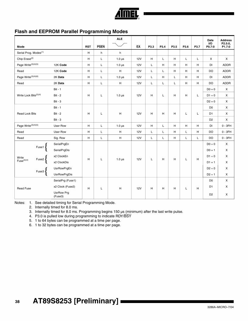
Notes: 1. See detailed timing for Serial Programming Mode.2. Internally timed for 8.0 ms.3. Internally timed for 8.0 ms. Programming begins 150 µs (minimum) after the last write pulse.4. P3.0 is pulled low during programming to indicate RDY/BSY5. 1 to 64 bytes can be programmed at a time per page.6. 1 to 32 bytes can be programmed at a time per page.
Flash and EEPROM Parallel Programming Modes
Mode RST PSEN
ALE
EA P3.3 P3.4 P3.5 P3.6 P3.7
Data I/O
P0.7:0
Address P2.5:0, P1.7:0
Serial Prog. Modes(1) H h h
Chip Erase(2) H L 1.0 µs 12V H L H L L X X
Page Write(3)(4)(5) 12K Code H L 1.0 µs 12V L H H H H DI ADDR
Read 12K Code H L H 12V L L H H H DO ADDR
Page Write(3)(4)(6) 2K Data H L 1.0 µs 12V L H L H H DI ADDR
Read 2K Data H L H 12V L L L H H DO ADDR
Write Lock Bits(2)(4)
Bit - 1
H L 1.0 µs 12V H L H H L
D0 = 0 X
Bit - 2 D1 = 0 X
Bit - 3 D2 = 0 X
Read Lock Bits
Bit - 1
H L H 12V H H H L L
D0 X
Bit - 2 D1 X
Bit - 3 D2 X
Page Write(3)(4)(5) User Row H L 1.0 µs 12V H L H H H DI 0 - 3FH
Read User Row H L H 12V L L H L H DO 0 - 3FH
Read Sig. Row H L H 12V L L H L L DO 0 - 3FH
Write Fuse(2)(4)
Fuse1SerialPrgEn
H L 1.0 µs 12V L H H L H
D0 = 0 X
SerialPrgDis D0 = 1 X
Fuse2x2 ClockEn D1 = 0 X
x2 ClockDis D1 = 1 X
Fuse3UsrRowPrgEn D2 = 0 X
UsrRowPrgDis D2 = 1 X
Read Fuse
SerialPrg (Fuse1)
H L H 12V H H H L H
D0 X
x2 Clock (Fuse2) D1 X
UsrRow Prg (Fuse3)
D2 X
38 AT89S8253 [Preliminary]3286A–MICRO–7/04

AT89S8253 [Preliminary]
Figure 18. Programming the Flash/EEPROM MemoryFigure 19. Verifying the Flash/EEPROM Memory
P1
P3.3
P3.5
P2.0 - P2.5
A0 - A7ADDR.
0000H/37FFH
SEE FLASHPROGRAMMINGMODES TABLE
3-24 MHz
A8 - A13P0
P3.4
PGMDATA
PROG
VPP
VIH
ALE
P3.6
P3.7
XTAL2 EA
RST
PSEN
XTAL1
GND
VCC
AT89S8253
P3.0 RDY/BSY(USE 10KPULLUP)
VCC
P1
P3.3
P3.5
P2.0 - P2.5
A0 - A7ADDR.
0000H/37FFH
SEE FLASHPROGRAMMINGMODES TABLE
3-24 Mhz
A8 - A13P0
VCC
P3.4
PGM DATA(USE 10KPULLUPS)
VI H
VI HALE
P3.6
P3.7
XTAL2 EA
RST
PSEN
XTAL1
GND
VCC
AT89S8253
VPP
393286A–MICRO–7/04
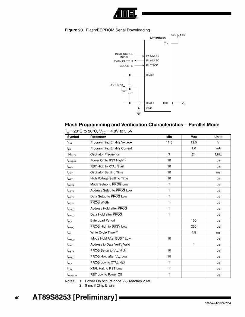
Figure 20. Flash/EEPROM Serial Downloading
Notes: 1. Power On occurs once VCC reaches 2.4V.2. 9 ms if Chip Erase.
Flash Programming and Verification Characteristics – Parallel ModeTA = 20°C to 30°C, VCC = 4.0V to 5.5V
Symbol Parameter Min Max Units
VPP Programming Enable Voltage 11.5 12.5 V
IPP Programming Enable Current 1.0 mA
1/tCLCL Oscillator Frequency 3 24 MHz
tPWRUP Power On to RST High (1) 10 µs
tRHX RST High to XTAL Start 10 µs
tOSTL Oscillator Settling Time 10 ms
tHSTL High Voltage Settling Time 10 µs
tMSTP Mode Setup to PROG Low 1 µs
tASTP Address Setup to PROG Low 1 µs
tDSTP Data Setup to PROG Low 1 µs
tPGW PROG Width 1 µs
tAHLD Address Hold after PROG 1 µs
tDHLD Data Hold after PROG 1 µs
tBLT Byte Load Period 150 µs
tPHBL PROG High to BUSY Low 256 µs
tWC Write Cycle Time(2) 4.5 ms
tMHLD Mode Hold After BUSY Low 10 µs
tVFY Address to Data Verify Valid 1 µs
tPSTP PROG Setup to VPP High 10 µs
tPHLD PROG Hold after VPP Low 10 µs
tPLX PROG Low to XTAL Halt 1 µs
tXRL XTAL Halt to RST Low 1 µs
tPWRDN RST Low to Power Off 1 µs
P1.7/SCK
DATA OUTPUT
INSTRUCTIONINPUT
CLOCK IN
3-24 MHz
4.0V to 5.5V
P1.5/MOSI
VIH
XTAL2
RSTXTAL1
GND
VCC
AT89S8253
P1.6/MISO
40 AT89S8253 [Preliminary]3286A–MICRO–7/04

AT89S8253 [Preliminary]
Figure 21. Flash/EEPROM Programming and Verification Waveforms – Parallel Mode
VC
C
RS
T
XTA
L 1
PS
EN
EA
/VP
P
ALE
/PR
OG
P3.
3...P
3.7
P1.
0...P
1.7
and
P2.
0...P
2.5
PO
RT
0
P3.
0(R
DY
/BS
Y)
t PW
RD
N
Run
ning
at 3
MH
z
t OS
TL
t HS
TL
t MS
TP
t PG
W
t AS
TP
t PS
TP
t DS
TP
t AH
LD t DH
LD
t BLT
t MH
LD
t MS
TP
t VF
Y
t XR
L
t PLX
t PH
LD
t WC
t PH
BL
AD
DR
0A
DD
R1
DAT
A0
DAT
A1
AD
DR
0A
DD
R1
DAT
A0
DAT
A1
t PW
RU
P
t RH
X
413286A–MICRO–7/04
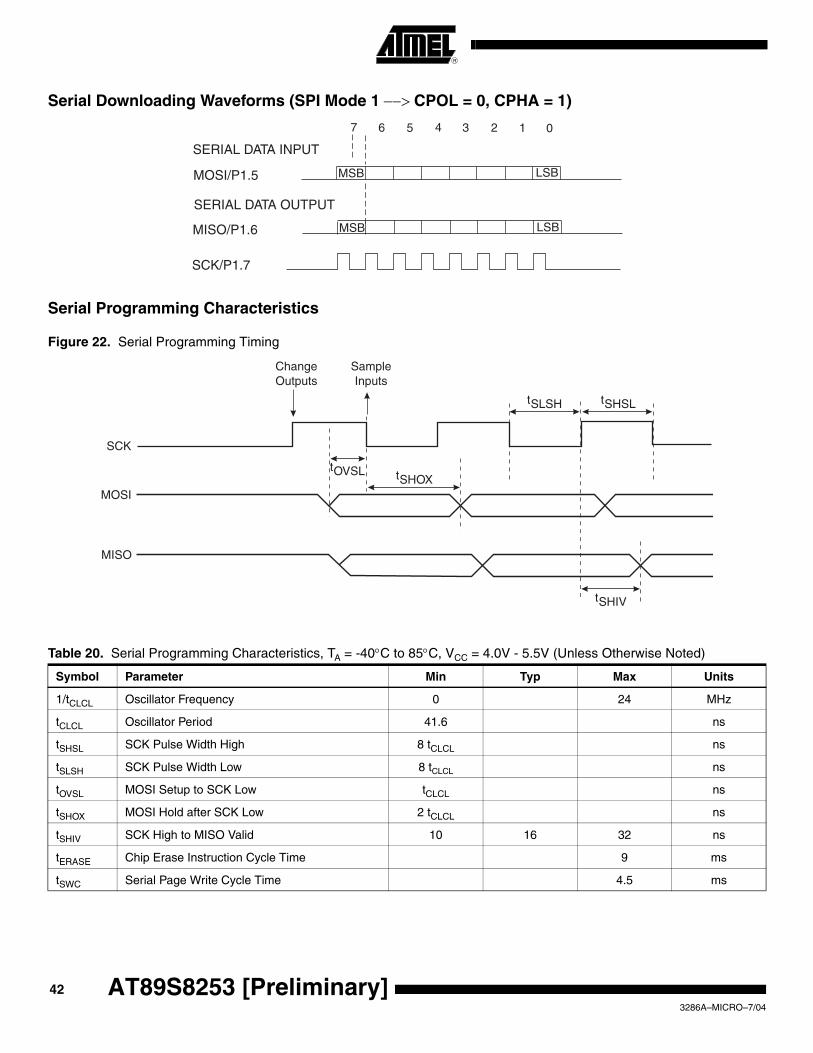
Serial Downloading Waveforms (SPI Mode 1 −−> CPOL = 0, CPHA = 1)
Serial Programming Characteristics
Figure 22. Serial Programming Timing
Table 20. Serial Programming Characteristics, TA = -40°C to 85°C, VCC = 4.0V - 5.5V (Unless Otherwise Noted)
Symbol Parameter Min Typ Max Units
1/tCLCL Oscillator Frequency 0 24 MHz
tCLCL Oscillator Period 41.6 ns
tSHSL SCK Pulse Width High 8 tCLCL ns
tSLSH SCK Pulse Width Low 8 tCLCL ns
tOVSL MOSI Setup to SCK Low tCLCL ns
tSHOX MOSI Hold after SCK Low 2 tCLCL ns
tSHIV SCK High to MISO Valid 10 16 32 ns
tERASE Chip Erase Instruction Cycle Time 9 ms
tSWC Serial Page Write Cycle Time 4.5 ms
SERIAL DATA INPUT
SCK/P1.7
MOSI/P1.5
MISO/P1.6
SERIAL DATA OUTPUT
01234567
MSB
MSB
LSB
LSB
SCK
MISO
MOSI
tOVSL
SHIVt
SHSLtSLSHt
SHOXt
ChangeOutputs
SampleInputs
42 AT89S8253 [Preliminary]3286A–MICRO–7/04
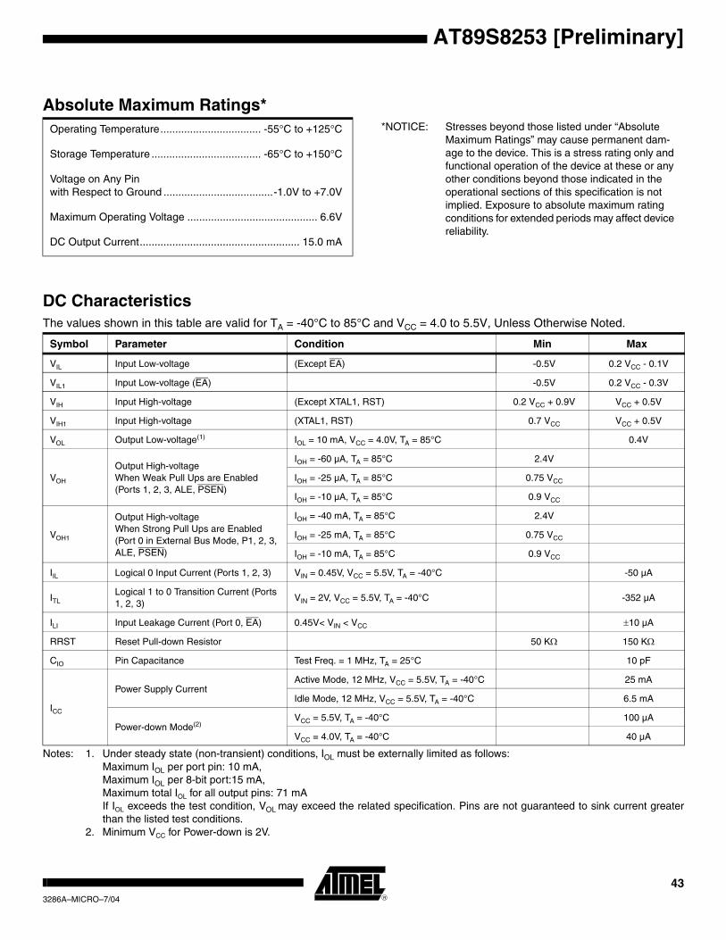
AT89S8253 [Preliminary]
Notes: 1. Under steady state (non-transient) conditions, IOL must be externally limited as follows: Maximum IOL per port pin: 10 mA, Maximum IOL per 8-bit port:15 mA, Maximum total IOL for all output pins: 71 mAIf IOL exceeds the test condition, VOL may exceed the related specification. Pins are not guaranteed to sink current greaterthan the listed test conditions.
2. Minimum VCC for Power-down is 2V.
Absolute Maximum Ratings*Operating Temperature.................................. -55°C to +125°C *NOTICE: Stresses beyond those listed under “Absolute
Maximum Ratings” may cause permanent dam-age to the device. This is a stress rating only and functional operation of the device at these or any other conditions beyond those indicated in the operational sections of this specification is not implied. Exposure to absolute maximum rating conditions for extended periods may affect device reliability.
Storage Temperature ..................................... -65°C to +150°C
Voltage on Any Pinwith Respect to Ground .....................................-1.0V to +7.0V
Maximum Operating Voltage ............................................ 6.6V
DC Output Current...................................................... 15.0 mA
DC CharacteristicsThe values shown in this table are valid for TA = -40°C to 85°C and VCC = 4.0 to 5.5V, Unless Otherwise Noted.
Symbol Parameter Condition Min Max
VIL Input Low-voltage (Except EA) -0.5V 0.2 VCC - 0.1V
VIL1 Input Low-voltage (EA) -0.5V 0.2 VCC - 0.3V
VIH Input High-voltage (Except XTAL1, RST) 0.2 VCC + 0.9V VCC + 0.5V
VIH1 Input High-voltage (XTAL1, RST) 0.7 VCC VCC + 0.5V
VOL Output Low-voltage(1) IOL = 10 mA, VCC = 4.0V, TA = 85°C 0.4V
VOH
Output High-voltage When Weak Pull Ups are Enabled(Ports 1, 2, 3, ALE, PSEN)
IOH = -60 µA, TA = 85°C 2.4V
IOH = -25 µA, TA = 85°C 0.75 VCC
IOH = -10 µA, TA = 85°C 0.9 VCC
VOH1
Output High-voltage When Strong Pull Ups are Enabled(Port 0 in External Bus Mode, P1, 2, 3, ALE, PSEN)
IOH = -40 mA, TA = 85°C 2.4V
IOH = -25 mA, TA = 85°C 0.75 VCC
IOH = -10 mA, TA = 85°C 0.9 VCC
IIL Logical 0 Input Current (Ports 1, 2, 3) VIN = 0.45V, VCC = 5.5V, TA = -40°C -50 µA
ITLLogical 1 to 0 Transition Current (Ports 1, 2, 3)
VIN = 2V, VCC = 5.5V, TA = -40°C -352 µA
ILI Input Leakage Current (Port 0, EA) 0.45V< VIN < VCC ±10 µA
RRST Reset Pull-down Resistor 50 KΩ 150 KΩ
CIO Pin Capacitance Test Freq. = 1 MHz, TA = 25°C 10 pF
ICC
Power Supply CurrentActive Mode, 12 MHz, VCC = 5.5V, TA = -40°C 25 mA
Idle Mode, 12 MHz, VCC = 5.5V, TA = -40°C 6.5 mA
Power-down Mode(2)VCC = 5.5V, TA = -40°C 100 µA
VCC = 4.0V, TA = -40°C 40 µA
433286A–MICRO–7/04
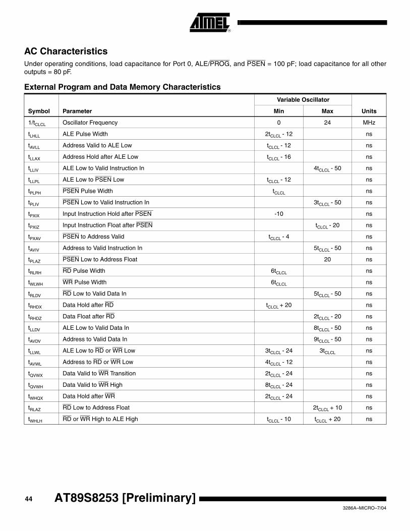
AC CharacteristicsUnder operating conditions, load capacitance for Port 0, ALE/PROG, and PSEN = 100 pF; load capacitance for all otheroutputs = 80 pF.
External Program and Data Memory Characteristics
Symbol Parameter
Variable Oscillator
UnitsMin Max
1/tCLCL Oscillator Frequency 0 24 MHz
tLHLL ALE Pulse Width 2tCLCL - 12 ns
tAVLL Address Valid to ALE Low tCLCL - 12 ns
tLLAX Address Hold after ALE Low tCLCL - 16 ns
tLLIV ALE Low to Valid Instruction In 4tCLCL - 50 ns
tLLPL ALE Low to PSEN Low tCLCL - 12 ns
tPLPH PSEN Pulse Width tCLCL ns
tPLIV PSEN Low to Valid Instruction In 3tCLCL - 50 ns
tPXIX Input Instruction Hold after PSEN -10 ns
tPXIZ Input Instruction Float after PSEN tCLCL - 20 ns
tPXAV PSEN to Address Valid tCLCL - 4 ns
tAVIV Address to Valid Instruction In 5tCLCL - 50 ns
tPLAZ PSEN Low to Address Float 20 ns
tRLRH RD Pulse Width 6tCLCL ns
tWLWH WR Pulse Width 6tCLCL ns
tRLDV RD Low to Valid Data In 5tCLCL - 50 ns
tRHDX Data Hold after RD tCLCL + 20 ns
tRHDZ Data Float after RD 2tCLCL - 20 ns
tLLDV ALE Low to Valid Data In 8tCLCL - 50 ns
tAVDV Address to Valid Data In 9tCLCL - 50 ns
tLLWL ALE Low to RD or WR Low 3tCLCL - 24 3tCLCL ns
tAVWL Address to RD or WR Low 4tCLCL - 12 ns
tQVWX Data Valid to WR Transition 2tCLCL - 24 ns
tQVWH Data Valid to WR High 8tCLCL - 24 ns
tWHQX Data Hold after WR 2tCLCL - 24 ns
tRLAZ RD Low to Address Float 2tCLCL + 10 ns
tWHLH RD or WR High to ALE High tCLCL - 10 tCLCL + 20 ns
44 AT89S8253 [Preliminary]3286A–MICRO–7/04

AT89S8253 [Preliminary]
External Program Memory Read Cycle
External Data Memory Read Cycle
453286A–MICRO–7/04
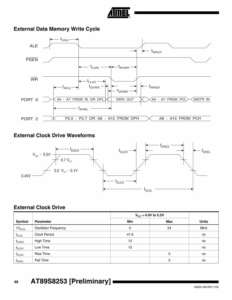
External Data Memory Write Cycle
External Clock Drive Waveforms
External Clock Drive
Symbol Parameter
VCC = 4.0V to 5.5V
UnitsMin Max
1/tCLCL Oscillator Frequency 0 24 MHz
tCLCL Clock Period 41.6 ns
tCHCX High Time 12 ns
tCLCX Low Time 12 ns
tCLCH Rise Time 5 ns
tCHCL Fall Time 5 ns
46 AT89S8253 [Preliminary]3286A–MICRO–7/04
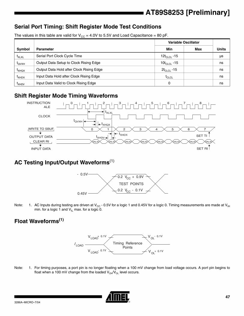
AT89S8253 [Preliminary]
Shift Register Mode Timing Waveforms
AC Testing Input/Output Waveforms(1)
Note: 1. AC Inputs during testing are driven at VCC - 0.5V for a logic 1 and 0.45V for a logic 0. Timing measurements are made at VIHmin. for a logic 1 and VIL max. for a logic 0.
Float Waveforms(1)
Note: 1. For timing purposes, a port pin is no longer floating when a 100 mV change from load voltage occurs. A port pin begins tofloat when a 100 mV change from the loaded VOH/VOL level occurs.
Serial Port Timing: Shift Register Mode Test ConditionsThe values in this table are valid for VCC = 4.0V to 5.5V and Load Capacitance = 80 pF.
Symbol Parameter
Variable Oscillator
UnitsMin Max
tXLXL Serial Port Clock Cycle Time 12tCLCL -15 µs
tQVXH Output Data Setup to Clock Rising Edge 10tCLCL -15 ns
tXHQX Output Data Hold after Clock Rising Edge 2tCLCL -15 ns
tXHDX Input Data Hold after Clock Rising Edge tCLCL ns
tXHDV Input Data Valid to Clock Rising Edge 0 ns
473286A–MICRO–7/04
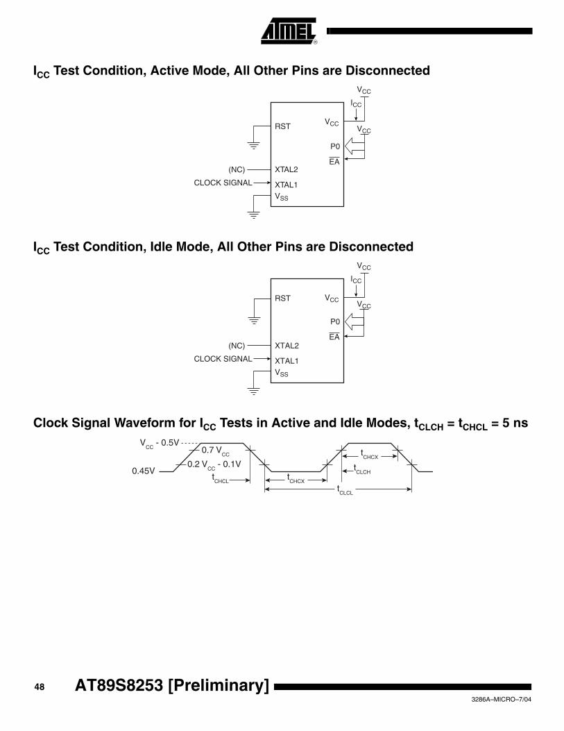
ICC Test Condition, Active Mode, All Other Pins are Disconnected
ICC Test Condition, Idle Mode, All Other Pins are Disconnected
Clock Signal Waveform for ICC Tests in Active and Idle Modes, tCLCH = tCHCL = 5 ns
XTAL2
RSTVCC
VCC
VCC
ICC
XTAL1
P0
EA
VSS
(NC)
CLOCK SIGNAL
XTAL2
RST VCC
VCC
VCC
ICC
XTAL1
P0
EA
VSS
(NC)
CLOCK SIGNAL
VCC
- 0.5V
0.45V0.2 V
CC - 0.1V
0.7 VCC
tCHCX
tCHCX
tCLCH
tCHCL
tCLCL
48 AT89S8253 [Preliminary]3286A–MICRO–7/04
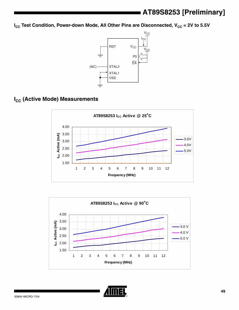
AT89S8253 [Preliminary]
ICC Test Condition, Power-down Mode, All Other Pins are Disconnected, VCC = 2V to 5.5V
ICC (Active Mode) Measurements
XTAL2
RST VCC
VCC
VCC
ICC
XTAL1
P0
EA
VSS
(NC)
AT89S8253 ICC Active @ 25oC
1.50
2.00
2.50
3.00
3.50
4.00
1 2 3 4 5 6 7 8 9 10 11 12
Frequency (MHz)
I CC
Act
ive
(mA
)
3.0V
4.0V
5.0V
AT89S8253 ICC Active @ 90oC
1.50
2.00
2.50
3.00
3.50
4.00
1 2 3 4 5 6 7 8 9 10 11 12
Frequency (MHz)
I CC
Act
ive
(mA
)
3.0 V
4.0 V
5.0 V
493286A–MICRO–7/04
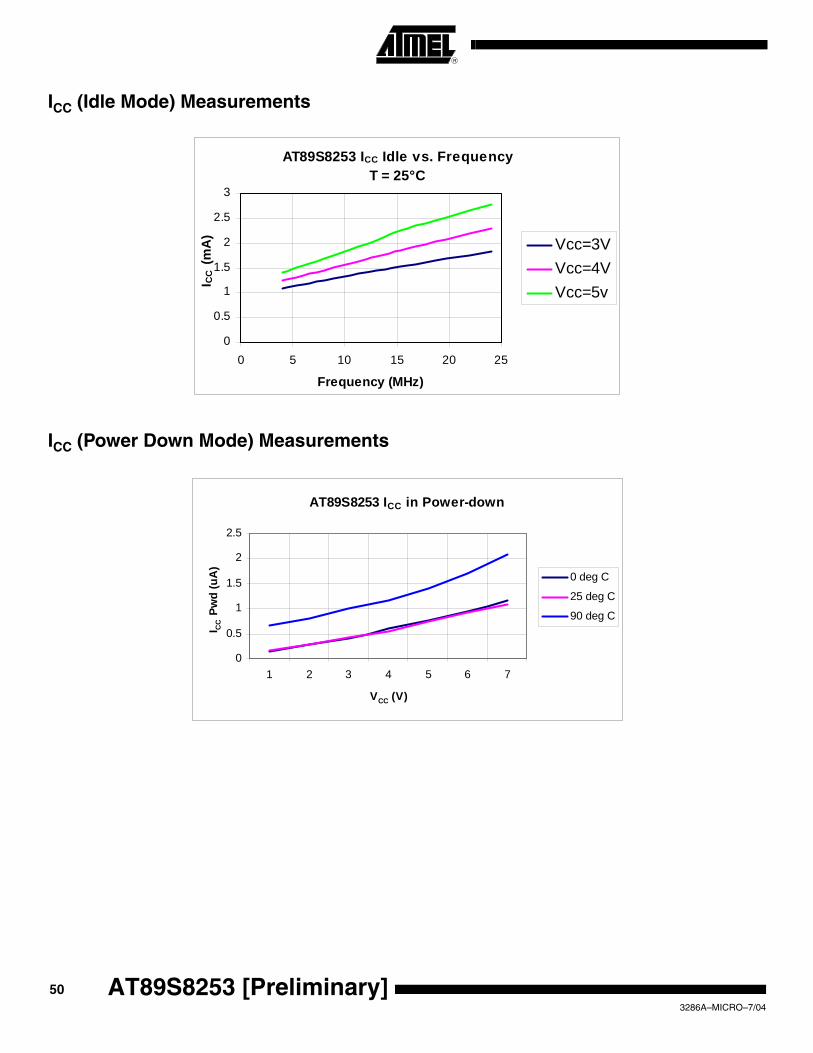
ICC (Idle Mode) Measurements
ICC (Power Down Mode) Measurements
AT89S8253 ICC Idle vs. FrequencyT = 25°C
0
0.5
1
1.5
2
2.5
3
0 5 10 15 20 25
Frequency (MHz)
I CC
(mA
) Vcc=3VVcc=4VVcc=5v
AT89S8253 ICC in Power-down
0
0.5
1
1.5
2
2.5
1 2 3 4 5 6 7
VCC (V)
I CC P
wd
(uA
)
0 deg C
25 deg C
90 deg C
50 AT89S8253 [Preliminary]3286A–MICRO–7/04

AT89S8253 [Preliminary]
Ordering Information Speed(MHz)
PowerSupply Ordering Code Package Operation Range
24 2.7V to 5.5V AT89S8253-24AC
AT89S8253-24JCAT89S8253-24PC
AT89S8253-24SC
44A
44J40P6
42PS6
Commercial
(0°C to 70°C)
2.7V to 5.5V AT89S8253-24AI
AT89S8253-24JI
AT89S8253-24PIAT89S8253-24SI
44A
44J
40P642PS6
Industrial
(-40°C to 85°C)
Package Type
44A 44-lead, Thin Plastic Gull Wing Quad Flat Package (TQFP)
44J 44-lead, Plastic J-leaded Chip Carrier (PLCC)
40P6 40-lead, 0.600" Wide, Plastic Dual Inline Package (PDIP)
42PS6 42-lead, 0.600" Wide, Plastic Dual Inline Package (PDIP)
513286A–MICRO–7/04
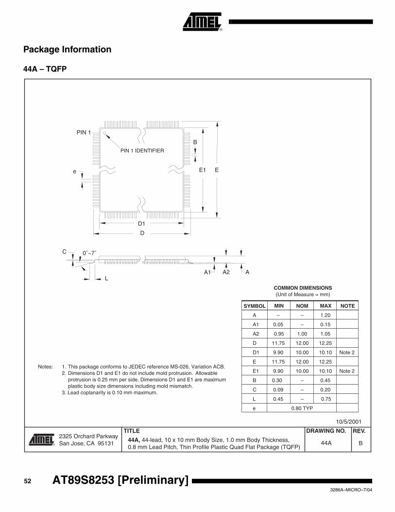
Package Information
44A – TQFP
2325 Orchard Parkway San Jose, CA 95131
TITLE DRAWING NO.
R
REV.
44A, 44-lead, 10 x 10 mm Body Size, 1.0 mm Body Thickness,0.8 mm Lead Pitch, Thin Profile Plastic Quad Flat Package (TQFP)
B44A
10/5/2001
PIN 1 IDENTIFIER
0˚~7˚
PIN 1
L
C
A1 A2 A
D1
D
e E1 E
B
COMMON DIMENSIONS(Unit of Measure = mm)
SYMBOL MIN NOM MAX NOTE
Notes: 1. This package conforms to JEDEC reference MS-026, Variation ACB. 2. Dimensions D1 and E1 do not include mold protrusion. Allowable
protrusion is 0.25 mm per side. Dimensions D1 and E1 are maximum plastic body size dimensions including mold mismatch.
3. Lead coplanarity is 0.10 mm maximum.
A – – 1.20
A1 0.05 – 0.15
A2 0.95 1.00 1.05
D 11.75 12.00 12.25
D1 9.90 10.00 10.10 Note 2
E 11.75 12.00 12.25
E1 9.90 10.00 10.10 Note 2
B 0.30 – 0.45
C 0.09 – 0.20
L 0.45 – 0.75
e 0.80 TYP
52 AT89S8253 [Preliminary]3286A–MICRO–7/04
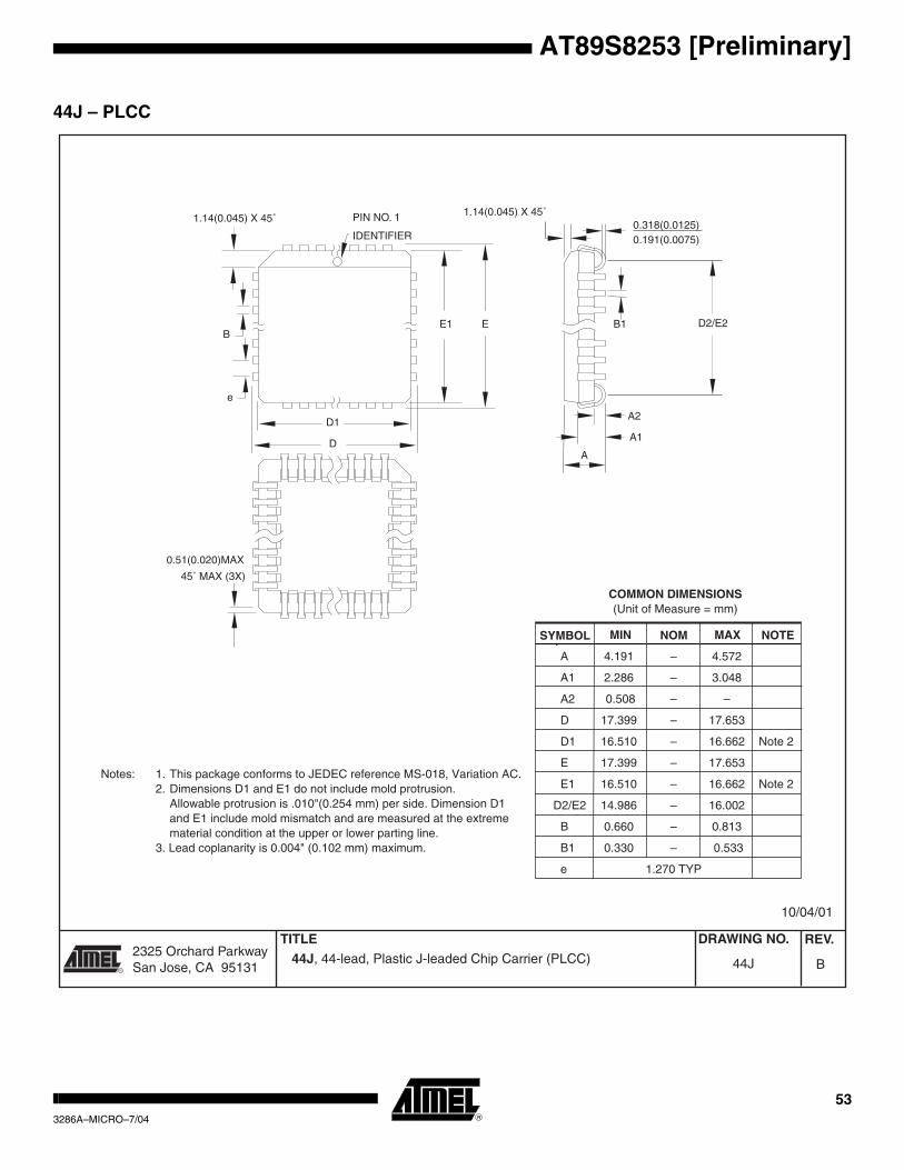
AT89S8253 [Preliminary]
44J – PLCC
Notes: 1. This package conforms to JEDEC reference MS-018, Variation AC. 2. Dimensions D1 and E1 do not include mold protrusion.
Allowable protrusion is .010"(0.254 mm) per side. Dimension D1and E1 include mold mismatch and are measured at the extremematerial condition at the upper or lower parting line.
3. Lead coplanarity is 0.004" (0.102 mm) maximum.
A 4.191 – 4.572
A1 2.286 – 3.048
A2 0.508 – –
D 17.399 – 17.653
D1 16.510 – 16.662 Note 2
E 17.399 – 17.653
E1 16.510 – 16.662 Note 2
D2/E2 14.986 – 16.002
B 0.660 – 0.813
B1 0.330 – 0.533
e 1.270 TYP
COMMON DIMENSIONS(Unit of Measure = mm)
SYMBOL MIN NOM MAX NOTE
1.14(0.045) X 45˚ PIN NO. 1
IDENTIFIER
1.14(0.045) X 45˚
0.51(0.020)MAX
0.318(0.0125)0.191(0.0075)
A2
45˚ MAX (3X)
A
A1
B1 D2/E2B
e
E1 E
D1
D
44J, 44-lead, Plastic J-leaded Chip Carrier (PLCC) B44J
10/04/01
2325 Orchard Parkway San Jose, CA 95131
TITLE DRAWING NO.
R
REV.
533286A–MICRO–7/04

40P6 – PDIP
2325 Orchard Parkway San Jose, CA 95131
TITLE DRAWING NO.
R
REV. 40P6, 40-lead (0.600"/15.24 mm Wide) Plastic Dual Inline Package (PDIP) B40P6
09/28/01
PIN1
E1
A1
B
REF
E
B1
C
L
SEATING PLANE
A
0º ~ 15º
D
e
eB
COMMON DIMENSIONS(Unit of Measure = mm)
SYMBOL MIN NOM MAX NOTE
A – – 4.826
A1 0.381 – –
D 52.070 – 52.578 Note 2
E 15.240 – 15.875
E1 13.462 – 13.970 Note 2
B 0.356 – 0.559
B1 1.041 – 1.651
L 3.048 – 3.556
C 0.203 – 0.381
eB 15.494 – 17.526
e 2.540 TYP
Notes: 1. This package conforms to JEDEC reference MS-011, Variation AC. 2. Dimensions D and E1 do not include mold Flash or Protrusion.
Mold Flash or Protrusion shall not exceed 0.25 mm (0.010").
54 AT89S8253 [Preliminary]3286A–MICRO–7/04

AT89S8253 [Preliminary]
42PS6 – PDIP
2325 Orchard Parkway San Jose, CA 95131
TITLE DRAWING NO.
R
REV. 42PS6, 42-lead (0.600"/15.24 mm Wide) Plastic Dual Inline Package (PDIP) A42PS6
11/6/03
PIN1
E1
A1
B
REF
E
B1
C
L
SEATING PLANE
A
0º ~ 15º
D
e
eB
COMMON DIMENSIONS(Unit of Measure = mm)
SYMBOL MIN NOM MAX NOTE
A – – 4.83
A1 0.51 – –
D 36.70 – 36.96 Note 2
E 15.24 – 15.88
E1 13.46 – 13.97 Note 2
B 0.38 – 0.56
B1 0.76 – 1.27
L 3.05 – 3.43
C 0.20 – 0.30
eB – – 18.55
e 1.78 TYP
Notes: 1. This package conforms to JEDEC reference MS-011, Variation AC. 2. Dimensions D and E1 do not include mold Flash or Protrusion.
Mold Flash or Protrusion shall not exceed 0.25 mm (0.010").
553286A–MICRO–7/04

Printed on recycled paper.
3286A–MICRO–7/04 xM
Disclaimer: Atmel Corporation makes no warranty for the use of its products, other than those expressly contained in the Company’s standardwarranty which is detailed in Atmel’s Terms and Conditions located on the Company’s web site. The Company assumes no responsibility for anyerrors which may appear in this document, reserves the right to change devices or specifications detailed herein at any time without notice, anddoes not make any commitment to update the information contained herein. No licenses to patents or other intellectual property of Atmel aregranted by the Company in connection with the sale of Atmel products, expressly or by implication. Atmel’s products are not authorized for useas critical components in life support devices or systems.
Atmel Corporation Atmel Operations
2325 Orchard ParkwaySan Jose, CA 95131, USATel: 1(408) 441-0311Fax: 1(408) 487-2600
Regional Headquarters
EuropeAtmel SarlRoute des Arsenaux 41Case Postale 80CH-1705 FribourgSwitzerlandTel: (41) 26-426-5555Fax: (41) 26-426-5500
AsiaRoom 1219Chinachem Golden Plaza77 Mody Road TsimshatsuiEast KowloonHong KongTel: (852) 2721-9778Fax: (852) 2722-1369
Japan9F, Tonetsu Shinkawa Bldg.1-24-8 ShinkawaChuo-ku, Tokyo 104-0033JapanTel: (81) 3-3523-3551Fax: (81) 3-3523-7581
Memory2325 Orchard ParkwaySan Jose, CA 95131, USATel: 1(408) 441-0311Fax: 1(408) 436-4314
Microcontrollers2325 Orchard ParkwaySan Jose, CA 95131, USATel: 1(408) 441-0311Fax: 1(408) 436-4314
La ChantrerieBP 7060244306 Nantes Cedex 3, FranceTel: (33) 2-40-18-18-18Fax: (33) 2-40-18-19-60
ASIC/ASSP/Smart CardsZone Industrielle13106 Rousset Cedex, FranceTel: (33) 4-42-53-60-00Fax: (33) 4-42-53-60-01
1150 East Cheyenne Mtn. Blvd.Colorado Springs, CO 80906, USATel: 1(719) 576-3300Fax: 1(719) 540-1759
Scottish Enterprise Technology ParkMaxwell BuildingEast Kilbride G75 0QR, Scotland Tel: (44) 1355-803-000Fax: (44) 1355-242-743
RF/AutomotiveTheresienstrasse 2Postfach 353574025 Heilbronn, GermanyTel: (49) 71-31-67-0Fax: (49) 71-31-67-2340
1150 East Cheyenne Mtn. Blvd.Colorado Springs, CO 80906, USATel: 1(719) 576-3300Fax: 1(719) 540-1759
Biometrics/Imaging/Hi-Rel MPU/High Speed Converters/RF Datacom
Avenue de RochepleineBP 12338521 Saint-Egreve Cedex, FranceTel: (33) 4-76-58-30-00Fax: (33) 4-76-58-34-80
Literature Requestswww.atmel.com/literature
© Atmel Corporation 2004. All rights reserved. Atmel® and combinations thereof are the registered trademarks of Atmel Corporation or itssubsidiaries. MCS® is the registered trademark of Intel Corporation. Other terms and product names may be the trademarks of others.


![Atmel AT89S8253 Data Sheet - Keil3 AT89S8253 [Preliminary] 3286A–MICRO–7/04 Pin Description VCC Supply voltage (all packages except 42-PDIP). GND Ground (all packages except 42-PDIP;](https://static.fdocuments.net/doc/165x107/60dd23df6697805a7823cf15/atmel-at89s8253-data-sheet-keil-3-at89s8253-preliminary-3286aamicroa704.jpg)