ASSGMT 2
54
Project Title: Design and Implementation of Microcontroller-Based Temperature Monitoring System Task 1: To describe basic block diagram of the s ystem structure. (To show overall flow of signals through the project) Answer: 8051 Hardware Architecture
Transcript of ASSGMT 2
8/8/2019 ASSGMT 2
http://slidepdf.com/reader/full/assgmt-2 1/54
Project Title: Design and Implementation of Microcontroller-Based Temperature
Monitoring System
Task 1: To describe basic block diagram of the system structure. (To show overall flow
of signals through the project)
Answer:
8051 Hardware Architecture
8/8/2019 ASSGMT 2
http://slidepdf.com/reader/full/assgmt-2 2/54
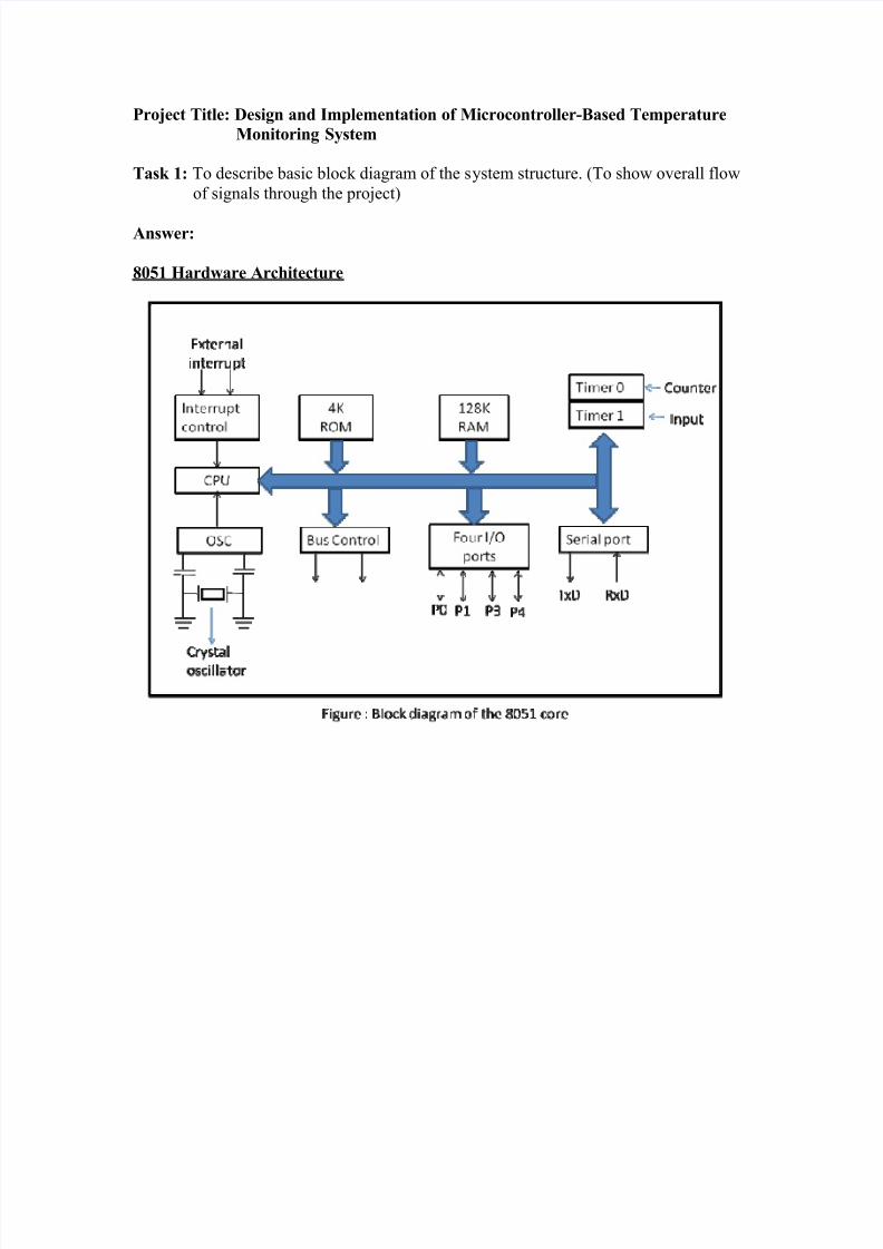
System structure
1. A microcomputer is design to monitor various processes (conveyer belt) on the
floor of a manufacturing plant, presented schematically in given figure.
2. A microcomputer has two input port addresses are F1H and F2H and output port
with addresses F3H. Input port F1H has 6 switches, 5 of which corresponding to
data line D4-D0 control the conveyer belt through the output port F3H.
3. Switch S7 corresponding to the data line D7, is reserved to indicate an energy on
the floor.
4. As a precautionary measured input port F2H is controlled by the foreman and its
switch, S7 is also used to indicate energy.
5. Output line D6 of port F3H is connected to the emergency alarm.
Special Function Register (SFR)

8/8/2019 ASSGMT 2
http://slidepdf.com/reader/full/assgmt-2 3/54
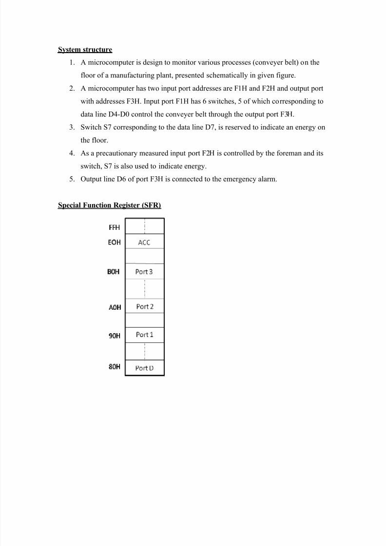
The circuit diagram of temperature monitoring of a cooker using 8051
microcontroller.
The monitoring process is:
1.
The temperature of the cooker is sensed by a temperature sensor LM352. The ADC0804 converts the analogue output voltage from the LM35 to an 8- bit digital value.
3. The digital value is then read by the 8051 microcontroller.
4. If a digital value of the cooker temperature over C r120 is read, the 8051
microcontroller will light up the Red LED, and otherwise it will light up the
Green LED.5. The steps (2) to (4) are repeated continuously.
8/8/2019 ASSGMT 2
http://slidepdf.com/reader/full/assgmt-2 4/54
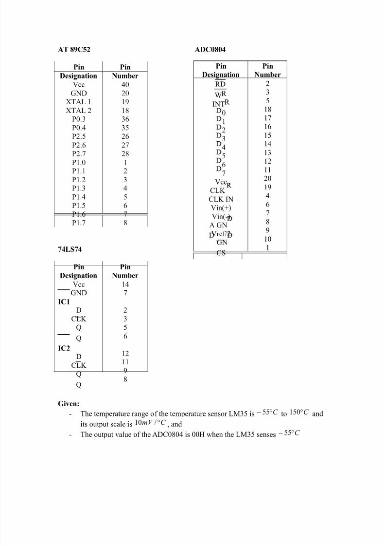
AT 89C52 ADC0804
Pin
Designation
Pin
Number
Vcc
GNDXTAL 1
XTAL 2P0.3
P0.4P2.5
P2.6P2.7
P1.0P1.1
P1.2
P1.3P1.4P1.5
P1.6P1.7
40
2019
1836
3526
2728
1 2
3
456
78
74LS74
Pin
Designation
Pin
Number
VccGND
IC1D
CLK Q
Q
IC2D
CLK Q
Q
147
2
35
6
1211
9
8
Given:
- The temperature range of the temperature sensor LM35 is C r 55 to C r150 and
its output scale is C mV r/10 , and
- The output value of the ADC0804 is 00H when the LM35 senses C r 55
Pin
Designation
Pin
Number
WINT
01
23
45
67
Vcc
CLK CLK INVin(+)
Vin(-)A GN
Vref /2GN
CS
2
3518
1716
1514
1312
11 20
19 4
67
89
101
8/8/2019 ASSGMT 2
http://slidepdf.com/reader/full/assgmt-2 5/54
8051 SERIAL COMMUNICATION
Computers transfer data in two ways: parallel and series. In parallel data transfers,often 8 or more lines (wire conductors) are used to transfer data to a device that is only a
few feet away. Examples of parallel transfer are printers and hard disks; each uses cables
with many wire strips. Although in such cases a lot of data can be transferred in a shortamount of time by using many wires in parallel, the distance cannot be great. To transfer to a device located many meters away, the serial method is used. In serial
communication, the data is sent one bit at a time, in contrast to parallel communication,in which the data is sent a byte or more at a time. Serial communication of the 8051 is the
topic of this chapter. The 8051 has serial communication capability built into it, therebymaking possible fast data transfer using only a few wires.
In this chapter we first discuss the basics of serial communication. In Section
10.2, 8051 interfacing to RS232 connectors via MAX232 line drives is discussed. Serialcommunication programming of the 8051 is discussed in Section 10.3.
SECTION 10.1: BASICS OF SERIAL COMMUNICATION
When microprocessor communicates with the outside world, it provides the datain byte-size chunks. In some cases, such as printers, the information is simply grabbed
from the 8-bit data bus and presented to 8-bit data bus of the printer. This can work onlyif the cable is not too long, since long cables diminish and even distort signals.
Furthermore, an 8-bit data path is expensive. For these reasons, serial communication isused for transferring data between two systems located at distance of hundreds of feet to
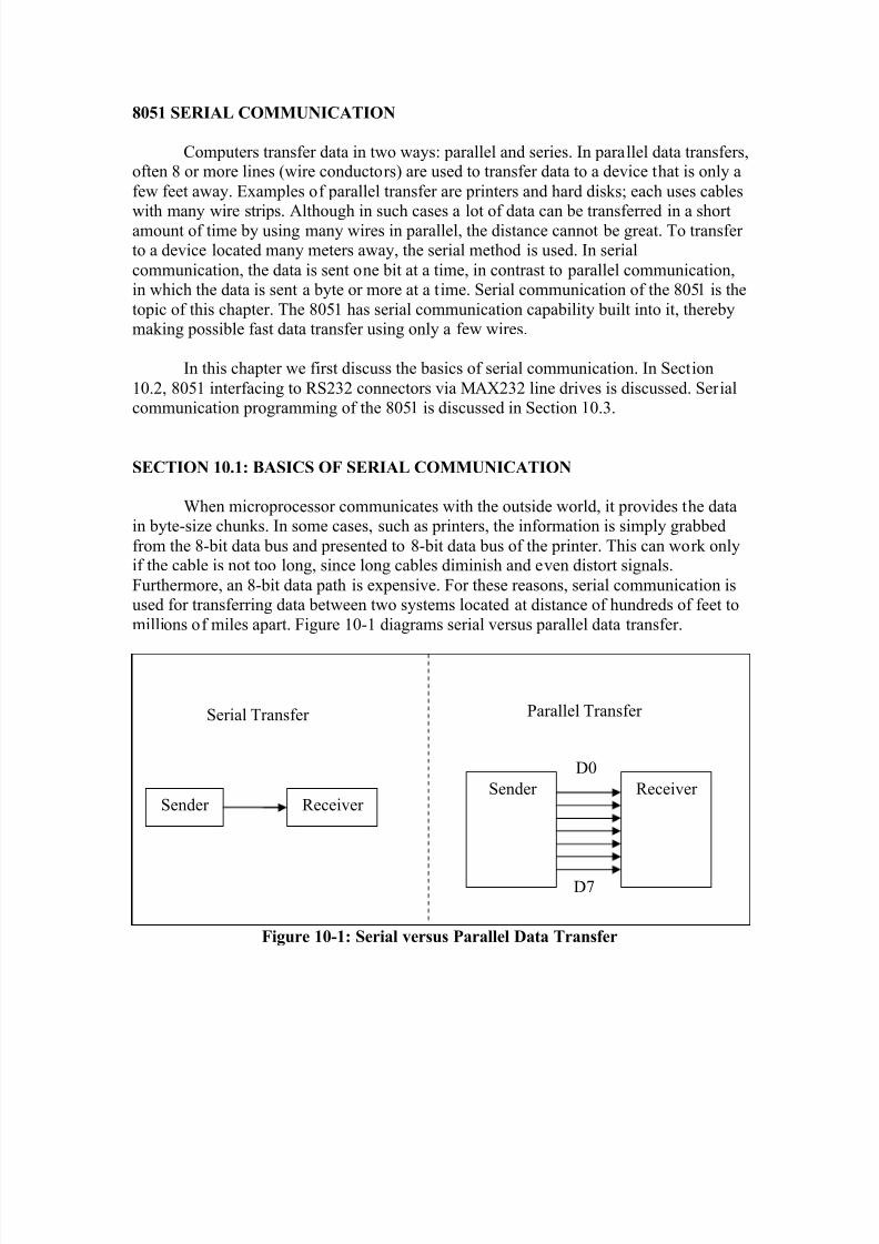
millions of miles apart. Figure 10-1 diagrams serial versus parallel data transfer.
Figure 10-1: Serial versus Parallel Data Transfer
Receiver Sender Receiver Sender
Serial Transfer
D0
D7
Parallel Transfer

8/8/2019 ASSGMT 2
http://slidepdf.com/reader/full/assgmt-2 6/54
The fact that in serial communication a single data line is used instead of the 8-bitdata line of parallel communication makes it not only much cheaper but also makes it
possible for two computers located in two different cities to communicate over thetelephone.
For serial data communication to work the byte of data must be converted to serial bits using a parallel-in-serial-out shift register; then it can be transmitted over a singledata line. This also means that at the receiving end there must be a serial-in-parallel-out
shift register to receive the serial data and pack them into a byte. Of course, if data is to be transferred on the telephone line, it must be converted from 0s and 1s to audio tones,
which are sinusoidal-shaped signals. This conversion is performed by a peripheral devicecalled a modem, which stands for ³modulator /demodulator.´
When the distance is short, the digital signal can be transferred as it is on a simple
wire and requires no modulation. This is how IBM PC keyboard transfer data to themotherboard. However, for long-distance data transfers using communication lines such
as a telephone, serial data communication requires a modem to modulate (convert from0s and 1s to audio tones) and demodulate (converting from audio tones to 0s and 1s).
Serial data communication uses two methods, asynchronous and synchronous.
The synchronous method transfers a block of data (characters) data a time and theasynchronous transfers a single byte at a time. It is possible to write software to use either
of these methods, but the programs can be tedious and long. For this reason, there arespecial IC chips made by many manufacturers for serial data communications. These
chips are commonly referred to as UART (universal asynchronous receiver-transmitter)and ASART (universal synchronous-asynchronous receiver-transmitter). The 8051 chip
has a built-in UART, which is discussed in detail in Section 10.3
Figure 10-2: Simplex, Half-, and Full-Duplex Transfer.
Transmitter
Transmitter
Transmitter
Transmitter
Transmitter
Receiver
Receiver
Receiver
Receiver
Receiver
Simplex
Half Duplex
Full Duplex

8/8/2019 ASSGMT 2
http://slidepdf.com/reader/full/assgmt-2 7/54
Half- and full-duplex transmission
In data transmission if the can be transmitted and received, it is a duplextransmission. This is in contrast to simplex transmissions such as with printers, in which
the computer only sends data. Duplex transmissions can be half or full duplex, depending
on whether or not the data transfer simultaneous. If data is transmitted one way at a time,it is referred to as half duplex. If the data can go both ways at the same time, it is fullduplex. Of course, full duplex requires two wire conductors for the data lines (in addition
to the signal ground (one for transmission and one for reception, in order to transfer andreceive data simultaneously. See Figure 10-2.
Asynchronous serial communication and data framing
The data coming in at the receiving end of the data line in a serial data transfer is
all 0s and 1s; it is difficult to make sense of the data unless the sender and receiver agreeon a set of rules, a protocol, on how the data is packed, how many bits constitute a
character, and when the data begins and ends.
Start and stop bits
Asynchronous serial data communication is widely used for character-orientedtransmissions, while block-oriented data transfers use the synchronous method. In the
asynchronous method, each character is placed in between start and stop bits. This iscalled framing. In data framing for asynchronous communications, the data, such as
ASCII characters, are packed in between a start bit and a stop bit. The start bit is alwaysone bit but the stop bit can be one or two bits. The start bit is always a 0 (low) and the
stop bit(s) is 1 (high). For example, look at Figure 10-3 in which the ASCII character ³A´(8-bit binary 0100 0001) is framed in between the start bit and a single stop bit. Notice
that the LSB is sent out first.
Figure 10-3: Framing ASCII ³A´ (41H)
Space
Goes out last
Stop
bit
0 0 0 0 01 0 1
Start bit
Goes out first
D7 D0 mark
8/8/2019 ASSGMT 2
http://slidepdf.com/reader/full/assgmt-2 8/54
Notice in Figure 10-3 that when there is no transfer, the signal 1 (high), which isreferred to as mark. The 0 (low) is referred to as space. Notice that the transmission
begins with a start bit followed by D0, the LSB, then the rest of the bits until MSB (D7),and finally, the one stop bit indicating the end of the character ³A´.
In asynchronous serial communications, peripheral chips and modems can be programmed for data that is 7 or 8 bits wide. This is in addition to the number of stop bits, 1 or 2. While in older systems ASCII characters were 7-bit, in recent years due to the
extended ASCII characters, 8-bit data has become common. In some older systems, dueto the slowness of the receiving mechanical device, two stop bits were used to give the
device sufficient time to organize itself before transmission of the next byte. However, inmodern PCs the use of one stop bit is standard. Assuming that we are transferring a text
file of ASCII characters using 1 stop bit, we have a total of 10 bits for each character: 8 bits for the ASCII code, and 1 bit each for the start and stop bits. Therefore, for each 8-bit
character there are an extra 2 bits, which gives 25% overhead.
In some systems in order to maintain data integrity, the parity bit of the character byte is included in the data frame. This means that for each character (7- or 8-bit,
depending on the system) we have a single parity bit in addition to start and stop bits. The parity bit is odd or even. In this case of an odd-parity bit the number of data bits,
including the parity bit, has an odd number of 1s. Similarly, in an even-parity bit systemthe total number of bits, including the parity bit, is even. For example, the ASCII
character ³A´, binary 0100 0001, has 0 for the even-parity bit. UART chips allow programming of the parity bit for odd-, even-, and no-parity options.
Data transfer rate
The rate of data transfer in serial data communication is stated in bps (bits per second). Another widely used terminology for bps is baud rate. However, the baud and
bps rates are not necessarily equal. This is due to the fact that baud rate is modemterminology and is defined as the number of signal changes per second. In modems, there
are occasions when a single change of signal transfers several bits of data. As far as theconductor wire is concerned, the baud rate and bps are the same, and for this reason in
this book we use the terms bps and baud interchangeably.
The data transfer rate of a given computer system depends on communication ports incorporated into that system. For example, the early IBM PC/XT could transfer
data at rate of 100 to 9600 bps. However in recent years, Pentium based PCs transfer dataat rates as high as 56K bps. It must be noted in asynchronous serial data communication,
the baud rate is generally limited to 100,000 bps.
8/8/2019 ASSGMT 2
http://slidepdf.com/reader/full/assgmt-2 9/54
Task 2: To design and develop the complete hardware circuit diagram which exploresreal-world applications of the microcontroller. (Interface microcontroller to
devices such as Keypad, LCD/LED, RS232 connector for serial communication,ADC/DAC, sensors, and relays/switches/actuators.)
Answer:
RS232 standards
To allow compatibility among data communication equipment made by various
manufacturers, an interfacing standard called RS232 was set by the Electronics industriesAssociation (EIA) in 1960. In 1963 it was modified and called RS232A. RS232B and
RS232C were issued in 1965 and 1969, respectively. In this book we refer to it simply asRS232. Today, RS232 is the most widely used serial I/O interfacing standard. This
standard is used in PCs and numerous types of equipment. However, since the standardwas set long before the advent of the TTL logic family, its input and output voltage levels
are not TTL compatible. In RS232, a 1 is represented by -3 to -25V
, while a 0 bit is +3 to+25V, making -3 to +3 undefined. For this reason, to connect any RS232 to a
microcontroller system we must use voltage converters such as MAX232 IC chips arecommonly referred to as line drivers.
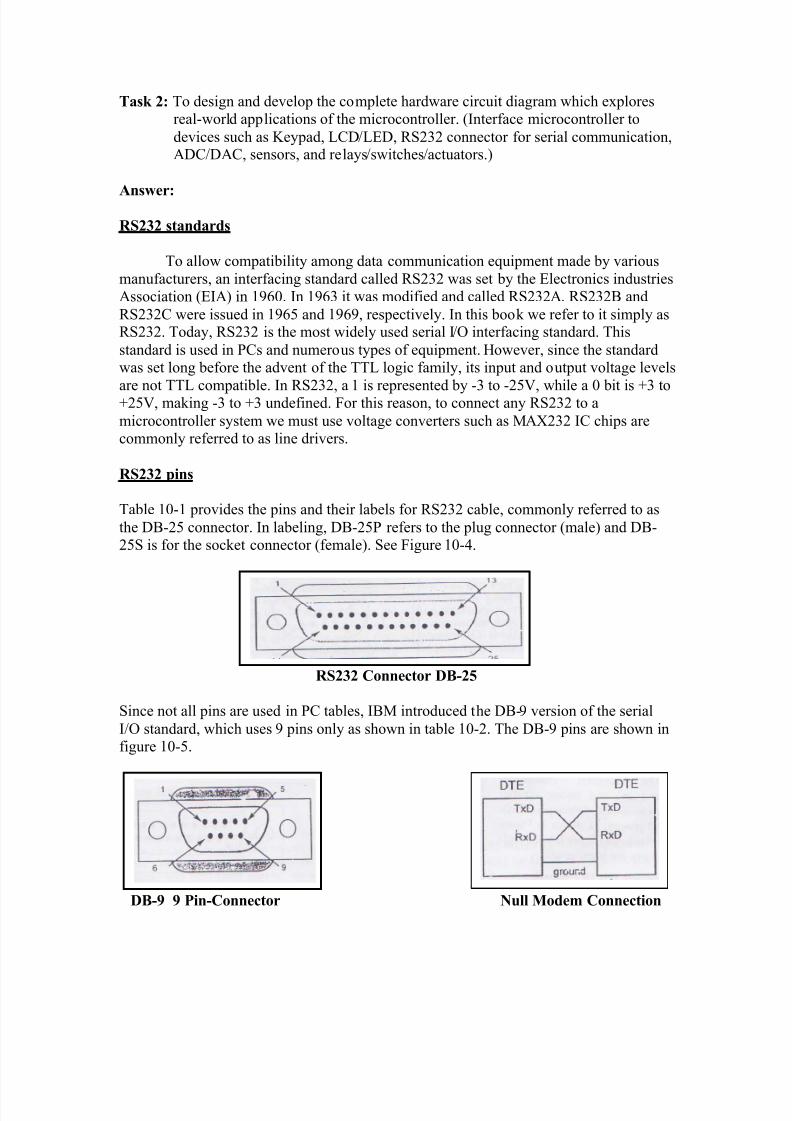
RS232 pins
Table 10-1 provides the pins and their labels for RS232 cable, commonly referred to as
the DB-25 connector. In labeling, DB-25P refers to the plug connector (male) and DB-25S is for the socket connector (female). See Figure 10-4.
RS232 Connector DB-25
Since not all pins are used in PC tables, IBM introduced the DB-9 version of the serial
I/O standard, which uses 9 pins only as shown in table 10-2. The DB-9 pins are shown infigure 10-5.
DB-9 9 Pin-Connector Null Modem Connection
8/8/2019 ASSGMT 2
http://slidepdf.com/reader/full/assgmt-2 10/54
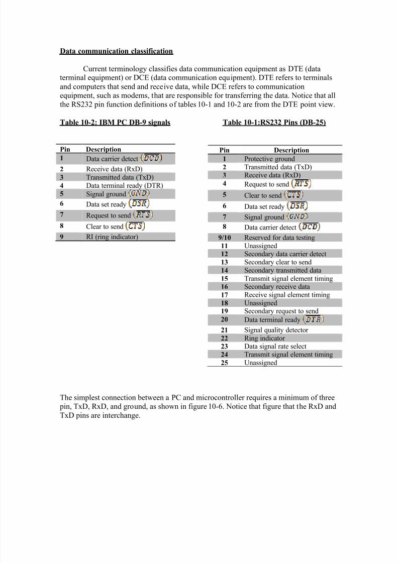
Data communication classification
Current terminology classifies data communication equipment as DTE (dataterminal equipment) or DCE (data communication equipment). DTE refers to terminals
and computers that send and receive data, while DCE refers to communication
equipment, such as modems, that are responsible for transferring the data. Notice that allthe RS232 pin function definitions of tables 10-1 and 10-2 are from the DTE point view.
Table 10-2: IBM PC DB-9 signals Table 10-1:RS232 Pins (DB-25)
Pin Description
1 Data carrier detect
2 Receive data (RxD)
3 Transmitted data (TxD)
4 Data terminal ready (DTR)
5 Signal ground6 Data set ready
7 Request to send
8 Clear to send
9 RI (ring indicator)
The simplest connection between a PC and microcontroller requires a minimum of three pin, TxD, RxD, and ground, as shown in figure 10-6. Notice that figure that the RxD and
TxD pins are interchange.
Pin Description
1 Protective ground
2 Transmitted data (TxD)3 Receive data (RxD)
4 Request to send
5 Clear to send6 Data set ready
7 Signal ground
8 Data carrier detect
9/10 Reserved for data testing
11 Unassigned12 Secondary data carrier detect
13 Secondary clear to send
14 Secondary transmitted data
15 Transmit signal element timing16 Secondary receive data
17 Receive signal element timing18 Unassigned19 Secondary request to send
20 Data terminal ready
21 Signal quality detector
22 Ring indicator 23 Data signal rate select
24 Transmit signal element timing
25 Unassigned
8/8/2019 ASSGMT 2
http://slidepdf.com/reader/full/assgmt-2 11/54
Examining RS232 handshaking signal
To ensure fast and reliable data transmission between two devices, the datatransfer must be coordinated. Just as in the case of the printer, due to the fact that in serial
data communication the receiving device may have no room for the data, there must be
away to inform the sender to stop sending data. Many of the pins of the RS232 connector are used for handshaking signals. Their only description is provided below only as areference and they can be passed since they are not supported by the 8051 UART chip.
1. DTR (data terminal ready).
When the terminal (or a PC COM port) is turned on, after going through a self-test, it sends s out signal DTR to indicate that it is ready for communication. If
there is something wrong with the COM port, this signal will not be activated.This is an active low signal and can be used to inform the modem that the
computer is alive and kicking. This is an output pin from DTE (PC COM port)and an input to the modem.
2. DSR (data set ready)
When DCE (modem) is turned on and has gone through the self-test, it asserts
DSR to indicate that it is ready to communicate. Thus, it is an output from themodem (DCE) and input to the PC (DTE). This is an active low signal. If for nay
reason the modem cannot make a connection to the telephone, this signal remainsinactive, indicating to the PC (or terminal) that it cannot accept or send data.
3. RTS (request to send)
When the DTE device (such as a PC) has a byte to transmit, it asserts RTS to
signal the modem that it has a byte of data to transmit. RTS is an active low
output from the DTE and an input to the modem.
4. CTS (clear to send)
In response to the RTS, when the modem has room for storing the data it is to
receive, it sends out signal CTS to the DTE (PC) to indicate that it can receive thedata now. This input signal to the DTE is used by the DTE to start transmission.
5. DCD (carrier detect or data carrier detect)
The modem asserts signal DCD to inform the DTE (PC) that a valid carrier has
been detected and that contact between it and the other modem is established.Therefore, DCD is an output from the modem and an input to the PC (DTE).
6. RI (ring indicator)
An output from the modem (DCE) and an input to a PC (DTE) indicates that thetelephone is ringing. It goes on and off in synchronization with the ringing sound.
Of the 6 handshake signals, this is the least often used, due to the fact thatmodems take care of answering the phone. However, if in a given system the PC
is in charge of answering the phone, this signal can be used.
8/8/2019 ASSGMT 2
http://slidepdf.com/reader/full/assgmt-2 12/54
From the above description, PC and modem communication can be summarizedas follows: while signals DTR and DSR are used by the PC and modem, respectively, to
indicate that they are alive and well, it is RTS and CTS that actually control the flow of data. When the PC wants to send data it asserts RTS, and in response, if the modem is
ready (has room) to accept the data, it send back CTS. If, for lack of room, the modem
does not active CTS, the PC will deassert DTR and try again. RTS and CTS are alsoreferred to as hardware control flow signals. This concludes the description of the 9 mostimportant pins of the RS232 handshake signal plus TxD, RxD, and ground is also
referred to as SG (signal ground)
8051 CONNECTION TO RS232
In this section, the details of the physical connections of the 8051 to RS232
connectors are given. As stated in Section 10.2, the RS232 standard is not TTLcompatible; therefore, it requires a line diver such as the MAX232 chip to convert RS232
voltage levels to TTL levels, and vice versa. The interfacing of 8051 with RS232connectors via the MAX232 chip is the main topic of this section.
RxD and TxD pins in the 8051
The 8051 has two pins that are used specifically for transferring and receiving
data serially. These two pins are called TxD and RxD and are part of the port 3 group(P3.0 and P3.1). Pin 11 of the 8051 (P3.1) is assigned to TxD and pin 10 (P3.0) is
designated as RxD. These pins are TTL compatible; therefore, they require a line driver to make them RS232 compatible. One such line driver is the MAX232 chip. This is
discussed next.
MAX232
Since the RS232 is not compatible with today¶s microprocessors andmicrocontrollers we need a line driver (voltage converter) to convert the RS232¶s signals
to TTL voltage levels that will be acceptable to the 8051¶s TxD and RxD pins. Oneexample of such a converter is MAX232from Maxim Corp. (www.maxim-ic.com). The
MAX232 converts from RS232 voltage levels to TTL voltage levels, and vice versa. Oneadvantage of the MAX232 chip is that is uses a +5V power source which is the same as
the source voltage for the 8051. In other words, with a single +5V power supply we can power both the 8051 and MAX232, with no need for the dual power supplies that are
common in many older systems.

8/8/2019 ASSGMT 2
http://slidepdf.com/reader/full/assgmt-2 13/54
(a) Inside MAX 232 and (b) its connection to the 8051 (Null Modem)
The line drivers used for TxD are called T1 and T2, while the line drivers for RxD
are designated as R 1 and R2. In many applications only one of each is used. For example,T1 and R 1 are used together for TxD and RxD of the 8051, and the second set is left
unused. Notice in MAX232 that the T1 line driver has a designation of T1in and T1outon pin numbers 11 and 14, respectively. The T1in pin is the TTL side and is connected to
TxD of the microcontroller, while T1out is the RS232 side that is connected to the RxD pin of the RS232 DB connector. The R 1 line driver has a designation of R 1in and R 1out
on pin numbers 13 and 12, respectively. The R 1in (pin13) is the RS232 side that isconnected to the TxD pin of the RS232 DB connector, and R 1out (pin 12) is the TTL side
that is connected to the RxD pin of the microcontroller. See figure 10-7. Notice the nulimodem connection where RxD for one is TxD for the other.
MAX232 requires four capacitors ranging from 1 to 22µF. the most widely used value for these capacitors is 22µF.
IBM PC/ compatible COM ports
IBM PC/ compatible computer based on x86 (8086, 286, 386, 486, and Pentium)microprocessor family normally have two COM ports. Both COM ports have RS232-type
connectors. Many PCs use n each of the DB-25 and DB-29 RS232 connectors. The COM ports are designated as COM 1 and COM 2. In recent years, COM 1 used for the mouse
and COM 2 is available for devices such as a modem. We cannot the 8051 serial port tothe COM 2 port of a PC for serial communication; we are ready to look at the 8051.
8/8/2019 ASSGMT 2
http://slidepdf.com/reader/full/assgmt-2 14/54
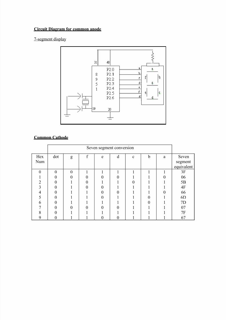
Circuit Diagram for common anode
7-segment display
Common Cathode
Seven segment conversion
Hex Num
dot g f e d c b a Sevensegment
equivalent0
1 2
34
56
78
9
0
00
00
00
00
0
0
01
1 1
1 1
01
1
1
00
01
1 1
01
1
1
01
00
01
01
0
1
01
1 0
1 1
01
0
1
1 0
1 1
1 1
1 1
1
1
1 1
1 1
00
1 1
1
1
01
1 0
1 1
1 1
1
3F
065B
4F66
6D7D
077F
67

8/8/2019 ASSGMT 2
http://slidepdf.com/reader/full/assgmt-2 15/54
Common Anode
Seven segment conversion
Hex
Num
dot g f e d c b a Seven
segmentequivalent
01
23
45
67
89
1 1
1 1
1 1
1 1
1 1
1 1
00
00
01
00
01
1 1
00
01
00
01
01
1 1
01
01
01
00
1 0
01
01
00
1 0
00
00
00
00
00
01
1 0
00
01
00
1 0
00
00
C0F9
A4B0
99 92
82F8
8098

8/8/2019 ASSGMT 2
http://slidepdf.com/reader/full/assgmt-2 16/54

8/8/2019 ASSGMT 2
http://slidepdf.com/reader/full/assgmt-2 17/54
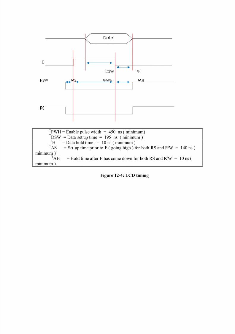
RS, register select
There are two very important registers inside the LCD. The RS pin is used for their selection as follows. If RS=0, the instruction command code register is selected,
allowing the user to send a command such as clear display cursor at home, etc. If RS=1
the data register is selected, allowing the user to send data to be displayed on the LCD.
RW, read/write.
R /W input allows the user to write information to the LCD or read informationfrom it. R /W=1 when reading; R /W=0 when writing.
E, enable
The enable pin is used by the LCD to latch information to its data pins. When datais supplied to data pins, a high-to-low pulse must be applied to this pin in order for the
LCD to latch in the data pins. This pulse must be a minimum of 450 ns wide.
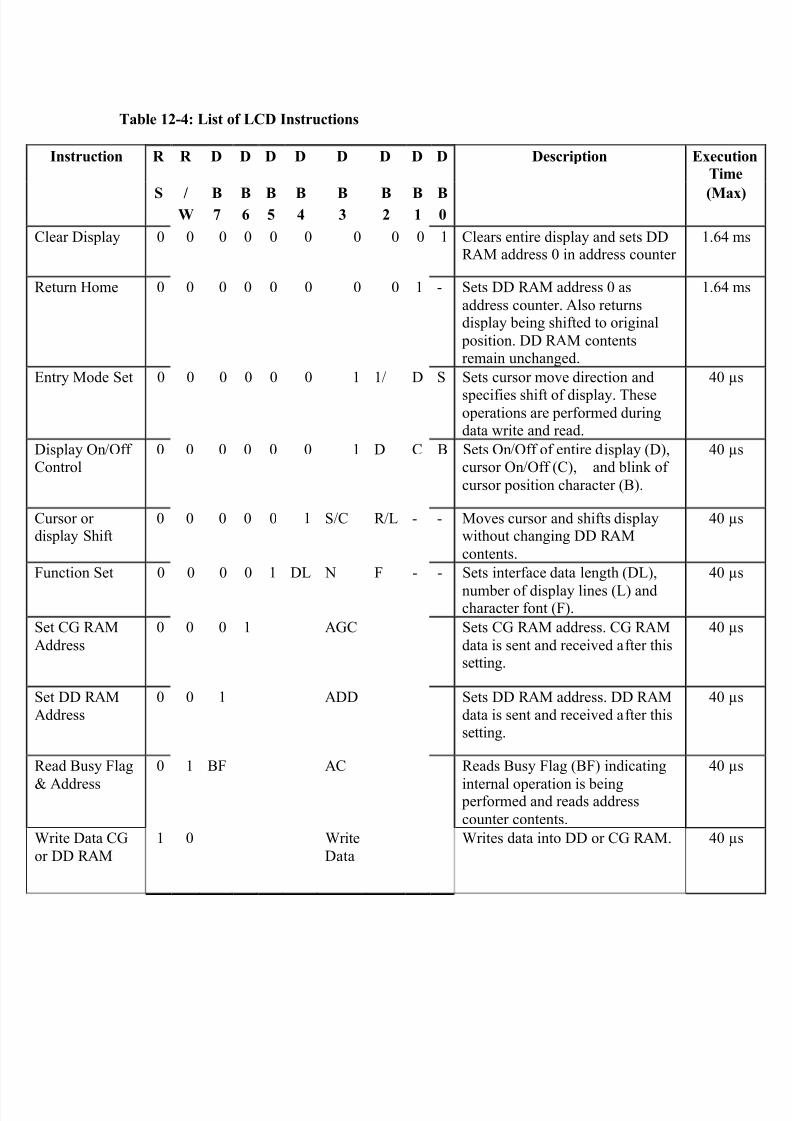
D0-D7 The 8-bit data pins, D0-D7, are used to send information to the LCD or read the
contents of the LCD¶s internal register. To display letters and numbers, we send ASCIIcodes for the letters A-Z, a-z and number 0-9 to these pins while making RS=1. There are
also instruction command codes that can be sent to the LCD to clear the display or forcethe cursor to the home position or blink the cursor. The tables 12-2 list the instruction
command codes.
Table 12-2: LCD Command Codes
(Hex) Register
1 Clear display screen
2 Return home
4 Decrement cursor (shift cursor to left)
6 Increment cursor (shift cursor to right)
5 Shift display right
7 Shift display left
8 Display off, cursor off
A Display off, cursor on
C Display on, cursor off
E Display on, cursor blinking
F Display on, cursor blinking
10 Shift cursor position to left
14 Shift cursor position to right
18 Shift the entire display to the right1C Shift the entire display to the left
80 Force cursor to beginning of 1st
line
C0 Force cursor to beginning of 2nd
line
38 2 lines and 5x7 matrix
8/8/2019 ASSGMT 2
http://slidepdf.com/reader/full/assgmt-2 18/54
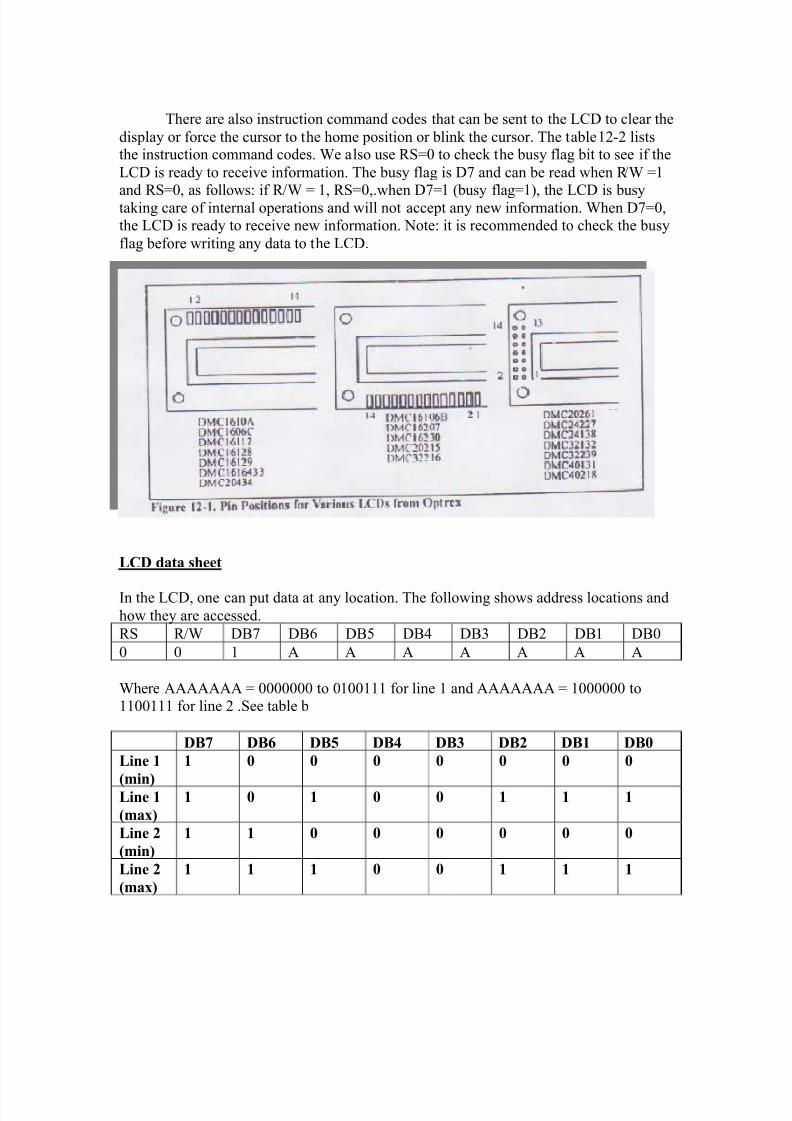
There are also instruction command codes that can be sent to the LCD to clear the
display or force the cursor to the home position or blink the cursor. The table 12-2 liststhe instruction command codes. We also use RS=0 to check the busy flag bit to see if the
LCD is ready to receive information. The busy flag is D7 and can be read when R /W =1
and RS=0, as follows: if R /W = 1, RS=0,.when D7=1 (busy flag=1), the LCD is busytaking care of internal operations and will not accept any new information. When D7=0,
the LCD is ready to receive new information. Note: it is recommended to check the busy
flag before writing any data to the LCD.
LCD data sheet
In the LCD, one can put data at any location. The following shows address locations and
how they are accessed.
RS R /W DB7 DB6 DB5 DB4 DB3 DB2 DB1 DB0
0 0 1 A A A A A A A
Where AAAAAAA = 0000000 to 0100111 for line 1 and AAAAAAA = 1000000 to1100111 for line 2 .See table b
DB7 DB6 DB5 DB4 DB3 DB2 DB1 DB0
Line 1
(min)
1 0 0 0 0 0 0 0
Line 1
(max)
1 0 1 0 0 1 1 1
Line 2
(min)
1 1 0 0 0 0 0 0
Line 2
(max)
1 1 1 0 0 1 1 1
8/8/2019 ASSGMT 2
http://slidepdf.com/reader/full/assgmt-2 19/54
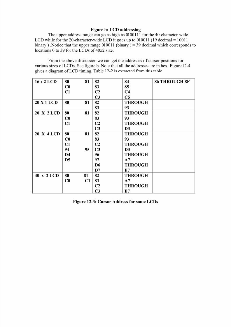
Figure b: LCD addressingThe upper address range can go as high as 0100111 for the 40-character-wide
LCD while for the 20-character-wide LCD it goes up to 010011 (19 decimal = 10011 binary ) .Notice that the upper range 010011 (binary ) = 39 decimal which corresponds to
locations 0 to 39 for the LCDs of 40x2 size.
From the above discussion we can get the addresses of cursor positions for various sizes of LCDs. See figure b. Note that all the addresses are in hex. Figure 12-4
gives a diagram of LCD timing. Table 12-2 is extracted from this table.
16 x 2 LCD 80 81
C0
C1
82
83
C2
C3
84
85
C4
C5
86 THROUGH 8F
20 X 1 LCD 80 81 82
83
THROUGH
93
20 X 2 LCD 80 81C0
C1
8283
C2
C3
THROUGH93
THROUGH
D3
20 X 4 LCD 80 81
C0
C1
94 95
D4
D5
82
83
C2
C3
96
97
D6
D7
THROUGH
93
THROUGH
D3
THROUGH
A7
THROUGH
E740 x 2 LCD 80 81
C0 C1
82
83
C2
C3
THROUGH
A7
THROUGH
E7
Figure 12-3: Cursor Address for some LCDs
8/8/2019 ASSGMT 2
http://slidepdf.com/reader/full/assgmt-2 20/54
TPWH = Enable pulse width = 450 ns ( minimum)TDSW = Data set up time = 195 ns ( minimum )TH = Data hold time = 10 ns ( minimum )
TAS = Set up time prior to E ( going high ) for both RS and R /W = 140 ns (
minimum )TAH = Hold time after E has come down for both RS and R /W = 10 ns (
minimum )
Figure 12-4: LCD timing
8/8/2019 ASSGMT 2
http://slidepdf.com/reader/full/assgmt-2 21/54
Table 12-4: List of LCD Instructions
Instruction R R D D D D D D D D Description Executi
Time
S / B B B B B B B B (MaxW 7 6 5 4 3 2 1 0
Clear Display 0 0 0 0 0 0 0 0 0 1 Clears entire display and sets DDR AM address 0 in address counter
1.64 m
Return Home 0 0 0 0 0 0 0 0 1 - Sets DD R AM address 0 as
address counter. Also returnsdisplay being shifted to original
position. DD R AM contentsremain unchanged.
1.64 m
Entry Mode Set 0 0 0 0 0 0 1 1/ D S Sets cursor move direction and
specifies shift of display. Theseoperations are performed duringdata write and read.
40 µs
Display On/Off Control
0 0 0 0 0 0 1 D C B Sets On/Off of entire display (D),cursor On/Off (C), and blink of
cursor position character (B).
40 µs
Cursor or display Shift
0 0 0 0 0 1 S/C R /L - - Moves cursor and shifts displaywithout changing DD R AM
contents.
40 µs
Function Set 0 0 0 0 1 DL N F - - Sets interface data length (DL),
number of display lines (L) andcharacter font (F).
40 µs
Set CG R AM
Address
0 0 0 1 AGC Sets CG R AM address. CG R AM
data is sent and received after thissetting.
40 µs
Set DD R AM
Address
0 0 1 ADD Sets DD R AM address. DD R AM
data is sent and received after thissetting.
40 µs
Read Busy Flag
& Address
0 1 BF AC Reads Busy Flag (BF) indicating
internal operation is being performed and reads address
counter contents.
40 µs
Write Data CG
or DD R AM
1 0 Write
Data
Writes data into DD or CG R AM. 40 µs
8/8/2019 ASSGMT 2
http://slidepdf.com/reader/full/assgmt-2 22/54
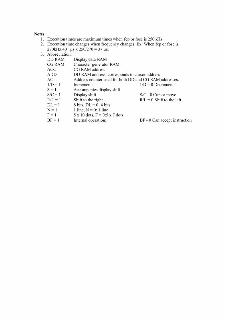
Notes:
1. Execution times are maximum times when fcp or fosc is 250 k Hz.2. Execution time changes when frequency changes. Ex: When fcp or fosc is
270k Hz:40 µs x 250/270 = 37 µs.
3. A bbreviation:DD R AM Display data R AMCG R AM Character generator R AM
ACC CG R AM addressADD DD R AM address, corresponds to cursor address
AC Address counter used for both DD and CG R AM addresses.1/D = 1 Increment 1/D = 0 Decrement
S = 1 Accompanies display shiftS/C = 1 Display shift S/C - 0 Cursor move
R /L = 1 Shift to the right R /L = 0 Shift to the leftDL = 1 8 bits, DL = 0: 4 bits
N = 1 1 line, N = 0: 1 lineF = 1 5 x 10 dots, F = 0:5 x 7 dots
BF = 1 Internal operation; BF - 0 Can accept instruction

8/8/2019 ASSGMT 2
http://slidepdf.com/reader/full/assgmt-2 23/54
8051 INTERFACING TO ADC
This section will explore interfacing ADC (analog-to-digital converter) chips and
temperature sensors to the 8051. First, we describe ADC chips, then show how tointerface an ADC to the 8051. Then we examine the characteristics of the LM35temperature sensor and show how to interface it to the 8051.
ADC devices
Analog-to-digital converters are among the most widely used devices for data
acquisition. Digital computers use binary (discrete) values, but in the physical worldeverything is analog (continuous). Temperature, pressure (wind or liquid), humidity and
velocity are a few examples of physical quantities that we deal with every day. A physical quantity is converted to electrical (voltage, current) signal using a device called
a transducer. Transducers are also referred to as sensors. Although there are sensors for temperature, velocity, pressure, light, and many other natural quantities, they produce an
output that is voltage (or current). Therefore, we need an analog-to-digital converter totranslate the analog signals to digital numbers so that the microcontroller can read them.
A widely used ADC chip is the ADC804.
ADC804 chip
The ADC804 IC is an analog ±to-digital converter in the family of the ADC800series from National Semiconductor. It is also available from many other manufacturers.
It works with +5 volts and has resolution of 8 bits. In addition to resolution, conversiontime is another major factor in judging an ADC. Conversion time is defined as the time it
takes the ADC to convert the analog input to a digital (binary) number. In the ADC804,the conversion time varies depending on the clocking signals applied to the CLK R and
CLK IN pins, but it cannot be faster than 110µs. the ADC804 pin descriptions follow.
CS
Chip select is an active low input used to activate the ADC804 chip. To access theADC804, this pin must be low.
RD (read)
This is an input signal and is active low. The ADC convert the analog input to is
binary equivalent and holds it in an internal register. RD is used to get the converted dataout of the ADC804 chip. When CS = 0, if a high-to-low pulse is applied to the RD pin,
the 8-bit digital output shows up at the D0 ± D7 data pins. The RD pin is also referred toas output enable.
8/8/2019 ASSGMT 2
http://slidepdf.com/reader/full/assgmt-2 24/54
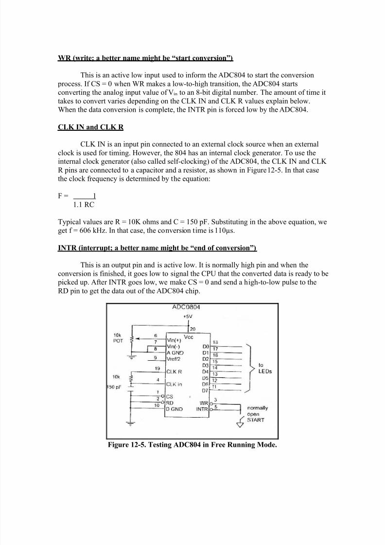
WR (write; a better name might be ³start conversion´)
This is an active low input used to inform the ADC804 to start the conversion
process. If CS = 0 when WR makes a low-to-high transition, the ADC804 starts
converting the analog input value of V
in to an 8-bit digital number. The amount of time ittakes to convert varies depending on the CLK IN and CLK R values explain below.When the data conversion is complete, the INTR pin is forced low by the ADC804.
CLK IN and CLK R
CLK IN is an input pin connected to an external clock source when an external
clock is used for timing. However, the 804 has an internal clock generator. To use theinternal clock generator (also called self-clocking) of the ADC804, the CLK IN and CLK
R pins are connected to a capacitor and a resistor, as shown in Figure 12-5. In that casethe clock frequency is determined by the equation:
F = 1
1.1 RC
Typical values are R = 10K ohms and C = 150 pF. Substituting in the above equation, weget f = 606 k Hz. In that case, the conversion time is 110µs.
INTR (interrupt; a better name might be ³end of conversion´)
This is an output pin and is active low. It is normally high pin and when the
conversion is finished, it goes low to signal the CPU that the converted data is ready to be picked up. After INTR goes low, we make CS = 0 and send a high-to-low pulse to the
RD pin to get the data out of the ADC804 chip.
Figure 12-5. Testing ADC804 in Free Running Mode.

8/8/2019 ASSGMT 2
http://slidepdf.com/reader/full/assgmt-2 25/54
Vin (+) and Vin (-)
These are the differential analog inputs where Vin = Vin (+) ± Vin (-).
Often the Vin (-) pin is connected to ground and the Vin (+) pin is used as the analog input
to be converted to digital.
VCC
This is the +5 volt power supply. It is also as a reference voltage when the Vref /2 input
(pin 9) is open (not connect). This is discussed next.Vref /2
Pin 9 is an input voltage used for the reference voltage. If this pin is open (notconnected), the analog input voltage for the ADC804 is in the range of 0 to 5 volts (the
same as the VCC pin). However, there are many applications where the analog inputapplied to Vin needs to be other than the 0 to +5V range. Vref /2 is used to implement
analog input voltages other than 0 ± 5 V. For example, if the analog input range needs to be 0 to 4 volts, Vref /2 is connected to 2 volts. Table 12-5 shows the Vin range for various
Vref /2 inputs.
Vref /2 (V) Vin (V) Step Size (mV)
Not connected* 0 to 5 5/256 = 19.53
2.0 0 to 4 4/255 = 15.62
1.5 0 to 3 3/256 = 11.71
1.28 0 to 2.56 2.56/256 = 10
1.0 0 to 2 2/256 = 7.81
0.5 0 to 1 1/256 = 3.90
Notes: V CC =5 V
*When not connected (open), V ref /2 (V) is measured at 2.5 volts for V CC = 5V.
Step size (resolution) is the smallest change that can be discerned by an ADC.

8/8/2019 ASSGMT 2
http://slidepdf.com/reader/full/assgmt-2 26/54
8/8/2019 ASSGMT 2
http://slidepdf.com/reader/full/assgmt-2 27/54
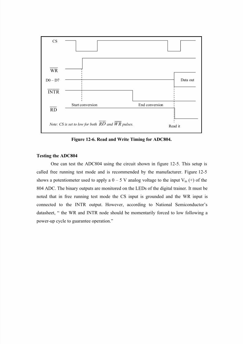
Figure 12-6. Read and Write Timing for ADC804.
Testing the ADC804
One can test the ADC804 using the circuit shown in figure 12-5. This setup is
called free running test mode and is recommended by the manufacturer. Figure 12-5
shows a potentiometer used to apply a 0 ± 5 V analog voltage to the input Vin (+) of the
804 ADC. The binary outputs are monitored on the LEDs of the digital trainer. It must be
noted that in free running test mode the CS input is grounded and the WR input is
connected to the INTR output. However, according to National Semiconductor¶s
datasheet, ³ the WR and INTR node should be momentarily forced to low following a
power-up cycle to guarantee operation.´
Read it
End conversionStart conversion
D0 ± D7
CS
R W
R T NI
DR
Data out
Note: CS is set to low for both
R and RW pulses.

8/8/2019 ASSGMT 2
http://slidepdf.com/reader/full/assgmt-2 28/54
8051
P2.5
P2.6
P1.0
P1.7
P2.7
ADC8045 V
150pF10k
10k
POT
D¡
VCC
¡ W CLK ¢
CLK IN
D0
Vin (+)
Vin (-)
A GND
Vref /2
GND
D7
INT¢
£ C

8/8/2019 ASSGMT 2
http://slidepdf.com/reader/full/assgmt-2 29/54
INTERFACING A TEMPERATURE SENSOR TO THE 8051
Transducers convert physical data such as temperature, light intensity, flow, and
speed to electrical signals. Depending on the transducer, the output produced is in the
form of voltage, current resistance, or capacitance. For example, temperature is converted
to electrical signals using a transducer called a thermistor. A thermistor responds to
temperature change by changing resistance, but its response is not linear, as seen in Table
12-6.
Table 12-6. Thermistor Resistance vs. Temperature.
Temperature (ºC) Tf (K ohms)
0 29.490
25 10.000
50 3.893
75 1.700
100 0.817
The complexity associated with writing software with such non-linear devices has
led many manufactures to market the linear temperature sensor. Simple and widely used
linear temperature sensors include the LM34 and LM35 series from National
Semiconductor Corp.
Table 12-7. LM35 Temperature Sensor Series Selection Guide.
Part Temperature Range Accuracy Output Scale
LM35A -55 ºC to +150 ºC +1.0 ºC 10 mV/F
LM35 -55 ºC to +150 ºC +1.5 ºC 10 mV/F
LM35CA -40 ºC to +110 ºC +1.0 ºC 10 mV/F
LM35C -40 ºC to +110 ºC +1.5 ºC 10 mV/F
LM35D 0 ºC to +100 ºC +2.0 ºC 10 mV/F
8/8/2019 ASSGMT 2
http://slidepdf.com/reader/full/assgmt-2 30/54
LM35 temperature sensors
The sensors of the LM35 series sensor are precision integrated-circuit temperature
sensors whose output voltage is linearly proportional to the Celsius (centrigate)
temperature. The LM35 requires no external calibration since it is inherently calibrated.
It outputs 10 mV for each degree of centigrade temperature. Table 12-8 is the selection
guide for the LM35.
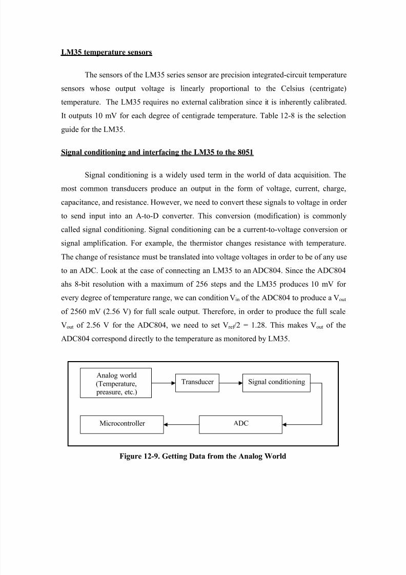
Signal conditioning and interfacing the LM35 to the 8051
Signal conditioning is a widely used term in the world of data acquisition. The
most common transducers produce an output in the form of voltage, current, charge,
capacitance, and resistance. However, we need to convert these signals to voltage in order
to send input into an A-to-D converter. This conversion (modification) is commonly
called signal conditioning. Signal conditioning can be a current-to-voltage conversion or
signal amplification. For example, the thermistor changes resistance with temperature.
The change of resistance must be translated into voltage voltages in order to be of any use
to an ADC. Look at the case of connecting an LM35 to an ADC804. Since the ADC804
ahs 8-bit resolution with a maximum of 256 steps and the LM35 produces 10 mV for
every degree of temperature range, we can condition Vin
of the ADC804 to produce a Vout
of 2560 mV (2.56 V) for full scale output. Therefore, in order to produce the full scale
Vout of 2.56 V for the ADC804, we need to set Vref /2 = 1.28. This makes Vout of the
ADC804 correspond directly to the temperature as monitored by LM35.
Figure 12-9. Getting Data from the Analog World
Analog world
(Temperature, preasure, etc.)
Transducer Signal conditioning
ADCMicrocontroller
8/8/2019 ASSGMT 2
http://slidepdf.com/reader/full/assgmt-2 31/54
Table 12-9. Temperature v. Vout of the ADC804
Temperature (ºC) Vin (mV) Vout (D7 ± D0)
0 0 0000 0000
1 10 0000 0001
2 20 0000 0010
3 30 0000 0011
10 100 0000 1010
30 300 0001 1110
Figure 12-10 shows connection of a temperature sensor to the ADC804. Notice
that we use the LM336-2.5 Zener diode to fix the voltage across the 10K pot at 2.5 volts.The use of the LM336-2.5 should overcome any fluctuations in the power supply.
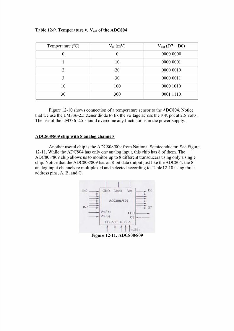
ADC808/809 chip with 8 analog channels
Another useful chip is the ADC808/809 from National Semiconductor. See Figure12-11. While the ADC804 has only one analog input, this chip has 8 of them. The
ADC808/809 chip allows us to monitor up to 8 different transducers using only a singlechip. Notice that the ADC808/809 has an 8-bit data output just like the ADC804. the 8
analog input channels re multiplexed and selected according to Table 12-10 using three
address pins, A, B, and C.
Figure 12-11. ADC808/809
8/8/2019 ASSGMT 2
http://slidepdf.com/reader/full/assgmt-2 32/54
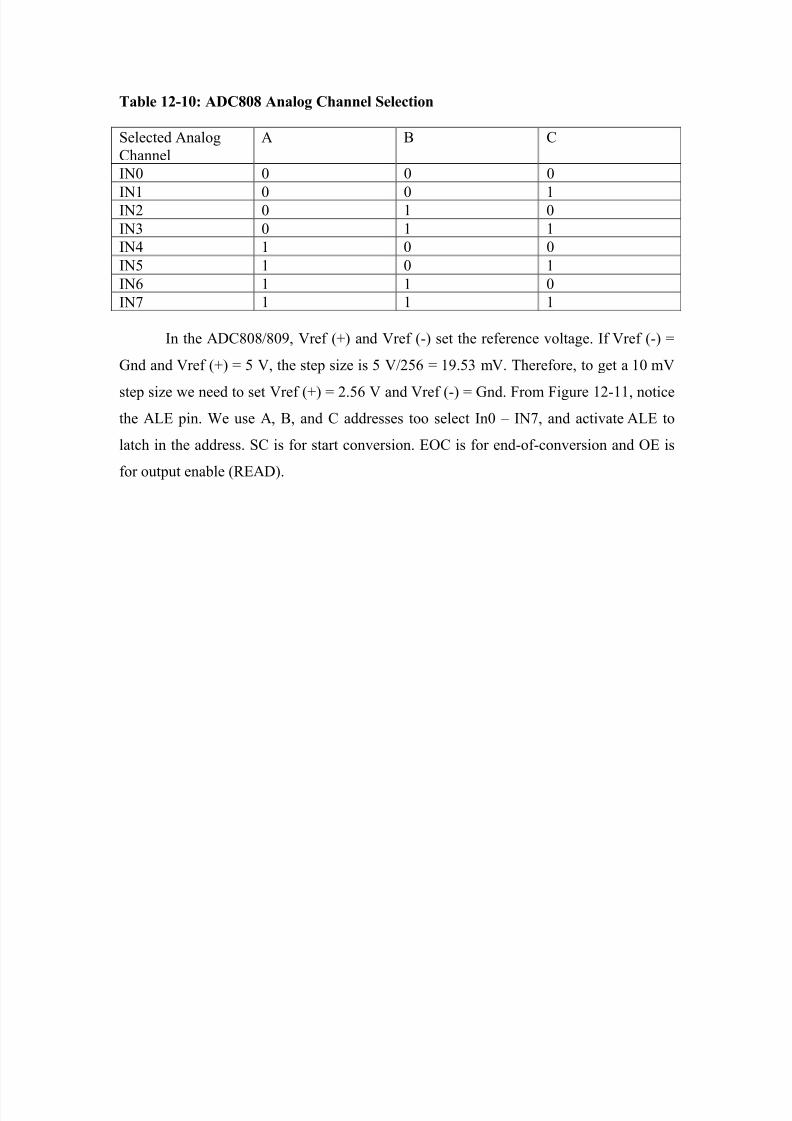
Table 12-10: ADC808 Analog Channel Selection
Selected Analog
Channel
A B C
IN0 0 0 0
IN1 0 0 1 IN2 0 1 0
IN3 0 1 1
IN4 1 0 0
IN5 1 0 1
IN6 1 1 0
IN7 1 1 1
In the ADC808/809, Vref (+) and Vref (-) set the reference voltage. If Vref (-) =
Gnd and Vref (+) = 5 V, the step size is 5 V/256 = 19.53 mV. Therefore, to get a 10 mV
step size we need to set Vref (+) = 2.56 V and Vref (-) = Gnd. From Figure 12-11, notice
the ALE pin. We use A, B, and C addresses too select In0 ± IN7, and activate ALE to
latch in the address. SC is for start conversion. EOC is for end-of-conversion and OE is
for output enable (READ).

8/8/2019 ASSGMT 2
http://slidepdf.com/reader/full/assgmt-2 33/54
INTERFACING TO THE KEYBOARD
Keyboard and LCDs are the most widely used input/output devices of the 8051,
and a basic understanding of them is essential.
Interfacing the keyboard to the 8051
At the lowest level, keyboards are organized in a matrix of rows and columns.
The CPU accesses both rows and columns through ports; therefore, with two 8-bit ports,
an 8 x 8 matrix of keys can be connected to a microprocessor. When a key is pressed, a
row and a column make a contact; otherwise, there is no connection between rows and
columns. In IBM PC keyboards, a single microcontroller takes care of hardware and
software interfacing of the keyboard. In such systems, it is the function of programs
stored in the EPROM of the microcontroller to scan the keys continuously, identify which
one has been activated, and present it to the motherboard.
Microcontroller Application
Numerical Keypads
R = Row
C = Column
1 2 3 A
4 5
9 87
B6
#0*
C
D
R 1 R2 R3 R4 C4C3C2C1
8/8/2019 ASSGMT 2
http://slidepdf.com/reader/full/assgmt-2 34/54
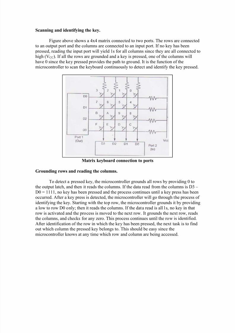
Scanning and identifying the key.
Figure above shows a 4x4 matrix connected to two ports. The rows are connectedto an output port and the columns are connected to an input port. If no key has been
pressed, reading the input port will yield 1s for all columns since they are all connected to
high (V
CC). If all the rows are grounded and a key is pressed, one of the columns willhave 0 since the key pressed provides the path to ground. It is the function of themicrocontroller to scan the keyboard continuously to detect and identify the key pressed.
Matrix keyboard connection to ports
Grounding rows and reading the columns.
To detect a pressed key, the microcontroller grounds all rows by providing 0 tothe output latch, and then it reads the columns. If the data read from the columns is D3 ±
D0 = 1111, no key has been pressed and the process continues until a key press has beenoccurred. After a key press is detected, the microcontroller will go through the process of
identifying the key. Starting with the top row, the microcontroller grounds it by providinga low to row D0 only; then it reads the columns. If the data read is all 1s, no key in that
row is activated and the process is moved to the next row. It grounds the next row, readsthe columns, and checks for any zero. This process continues until the row is identified.
After identification of the row in which the key has been pressed, the next task is to findout which column the pressed key belongs to. This should be easy since the
microcontroller knows at any time which row and column are being accessed.
8/8/2019 ASSGMT 2
http://slidepdf.com/reader/full/assgmt-2 35/54
Algorithm
1. Function of the microcontroller to scan the keyboard continuously to detect andidentify the key pressed.
2. Microcontroller reads the columns (digits).
3.
If the data (digital 4bits) read from the columns is D3 - D0 = 1111, no key has been pressed.4. This process continues until a key press is detected.
5. Microcontroller reads D3 ~ D0 = 1101, this means that a key in column one (C1 =D1) has been pressed.
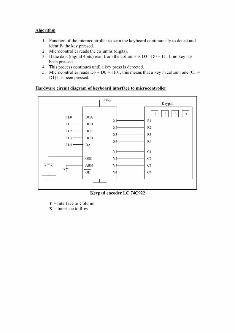
Hardware circuit diagram of keyboard interface to microcontroller
Keypad encoder I.C 74C922
Y = Interface to ColumnX = Interface to Row
1 2 3 4
R 1
R2
R3
R4
C1
C2
C3
C4
X3
X4
Y1
Y2
Y3
Y4
X2
X1 DOA
DOB
DOC
DOD
DA
OE
ABM
OSC
P1.0
P1.1
P1.2
P1.3
P1.4
+VccKeypad

8/8/2019 ASSGMT 2
http://slidepdf.com/reader/full/assgmt-2 36/54
74C922 Keypad Encoder Truth Table
Key
pressed
DA DOD
23
DOC
22
DOB
21
DOA
20
Hex
4 bit
1 1 0 0 0 0 0
2 1 0 0 0 1 1 3 1 0 0 1 0 2
A 1 0 0 1 1 3
4 1 0 1 0 0 4
5 1 0 1 0 1 5
6 1 0 1 1 0 6
B 1 0 1 1 1 7
7 1 1 0 0 0 8
8 1 1 0 0 1 9
9 1 1 0 1 0 A = 1010
C 1 1 0 1 1 B = 1011
* 1 1 1 0 0 C = 11000 1 1 1 0 1 D = 1101
# 1 1 1 1 0 E = 1110
D 1 1 1 1 1 F = 1111
Keypad
pressed
0 Z Z Z Z

8/8/2019 ASSGMT 2
http://slidepdf.com/reader/full/assgmt-2 37/54
Program given 13-1 is the 8051 Assembly language program for detection and
identification of key activation. In this program, it is assumed that P1 and P2 are
initialized as output and input, respectively. Program 13-1 goes through the following
four major stages:
1. To make sure that the preceding key has been released, 0s are output to all rows at
once, and the columns are read and checked repeatedly until all the columns are
high. When all columns are found to be high, the program waits for a short amount
of time before it goes to the next stage of waiting for a key to be pressed.
2. To see if any key is pressed, the columns are scanned over and over in an infinite
loop until one of them has a 0 on it. Remember that the output latches connected to
rows still have their initial zeros (provided in stage 1), making them grounded, after
the key press detection, it waits 20 ms for the bounce and then scans the columns
again. This serves two functions:
1. It ensures that the first key press detection was not an erroneous one due to
a spike noise.
2. The 20 ms delay prevents the same key press from being interpreted as
multiple key presses. If after the 20 ms delay the key is still pressed, it
goes to the next stage to detect which row it belongs to; otherwise, it goes
back into the loop to detect a real key press
3. To detect which row the key press belongs to, it grounds one row at a time, reading
the columns each time. If it finds that all columns are high, this means that the key
press cannot belong to that row; therefore, it grounds the next row and continues
until it finds the row the key press belongs to. Upon finding the row that the key
press belongs to, it sets up the starting address for the look-up table holding the scan
codes (or the ASCII value) for that row and goes to the next stage to identify the
key.
4. To identify the key press, it rotates the column bits, one bit at a time, into the carry
flag and checks to see if it is low. Upon finding the zero, it pulls out the ASCII code
for that key from the look-up table; otherwise, it increments the pointer to point to
the next element of the look-up table. Figure 13-6 flowcharts this process.

8/8/2019 ASSGMT 2
http://slidepdf.com/reader/full/assgmt-2 38/54
Keyboard scanning flow chart
While the key is press detection is standard for all keyboards, the process for
determining which key is pressed varies. The look-up table method, shown in Program13-1 can be modified to work with any matrix up to 8 x 8. Figure 13-6 provides the
flowchart for program 13-1 for scanning and identifying the pressed key.

8/8/2019 ASSGMT 2
http://slidepdf.com/reader/full/assgmt-2 39/54
Task 3: To design and develop assembly language software which explores real-worldapplications of the microcontroller. (Interface microcontroller to devices such as
Keypad, LCD/LED, RS232 connector for serial communication, ADC/DAC,sensors, and relays/switches/actuators.)
Answer:
8051 SERIAL COMMUNICATION PROGRAMMING
In this section we discuss the serial communication registers of the 8051 and show how
to program them to transfer and receive data serially. Since IBM PC/compatiblecomputers are so widely used to communicate with 8051-based systems, we will
emphasize serial communications of the 8051 with the COM port of the PC. To allowdata transfer between the PC and an 8051 system without any error, we must make sure
that the baud rate of the 8051 system matches the baud rate of the PC¶s COM port. The baud rates supported by PC BIOS are listed in Table10-3. You can examine these baud
rates by going to the Windows Terminal program and clicking on the CommunicationSettings option. The terminal.exe program comes with Windows 3.1 and an iso works in
Windows 95 and 98. In Windows 95 and higher you can use the HyperTerminal function.HyperTerminal supports baud rates much higher than the ones listed in table 10-3.
Table10-3: PC
Baud Rates
110
150
300
600
12002400
4800
9600
19200
Band Rate TH1 (Decimal) TH1 ( HEX)
9600 -3 FD
4800 -6 FA
2400 -12 F41200 -24 E8
Figure: 10-4 Timer 1 TH1 register values for various band rates
8/8/2019 ASSGMT 2
http://slidepdf.com/reader/full/assgmt-2 40/54
BAUD RATE IN THE 8051
The 8051 transfers and receives data serially at many different band rates, the band rate in the 8051 is programmable. This is done with the help of timer 1. Before we
discuss how to do that, we will look at the relationship between the crystal frequency and
the band rate in the 8051.As discussed in previous chapters, the 8051 devides the crystal frequency by 12 toget the machine cycle frequency . in the case of XTAL = 11.0592Mhz. the machine cycle
frequency is 921.6k Hz (11.0592MHz/12 = 921.6 k Hz) . the 8051¶s serial communicationUART circuitry devides the machine cycle frequency of 921.6k Hz by 32 once more
before it is used by timer 1 to set the band, rate. Therefore m 921,6k Hz divided by 31 gives 28,800 Hz. This is the number we will use throughout this section to find the timer
I value to set the band rate. When timer 1 is used to set the band rate is must be programmed in mode 1 , that is 8-bit,auto reload. To get band rates compatible with the
PC, we must load TH1 with the values shown in table 10-3.
SBUF register.
SBUF is an 8-bit register used solely for serial communication in the 8051. For a byte of
data to be transferred via the TxD line it must be placed in the SBUF register. Similarly,SBUF holds the byte if data when it is received by the 8051¶s R x D line . SBUF holds
the byte of data when it is received by the 8051¶s R x D line. SBUF can be accessed likeany other register in the 8051.Look at the following examples of how this register is
accessed :
MOV SBUF, #¶D¶ ;load SBUF = 44H ,ASCII for D¶MOV SBUF ,A ;copy accumulator into SBUF
MOV A,SBUF ;copy SBUF into accumulator]
The moment a byte is written into SBUF , it is framed with the start and stop bits andtransferred serially via the T D pin. Similarly, when then bits are received serially via R
x D line . SBUF can be accessed line any other register in the 8051 deframes. It byeliminating the stop and start bits, making a byte out of data received, and then placing it
in the SBUF.

8/8/2019 ASSGMT 2
http://slidepdf.com/reader/full/assgmt-2 41/54
SCON (serial control) register
The SCON register is an 8 bit register used to program the start bit, stop bit, anddata bits of data framing, among other things.
The following describes various bits of the SCON register.
SM0 SM1 SM2 REN TB8 RB8 T1 R 1
SM0 SCON.7 serial port mode specific
SM1 SCON.6 serial port mode specificSM2 SCON.5 used for multiprocessor communication ( make it 0)
REN SCON.4 set/cleared by software to enable/disable receptionTB8 SCON.3 Not widely used
RB8 SCON.2 not widely usedT1 SCON.1 transmit interrupt flag. Set by hardware at the beginning of
the stop bitin mode 1 . Must be cleared by software.
R 1 SCON.0 Receive interrupt flag. Set by hardware halfway through
the stop bittime in mode 1. Must be cleared by software.
Figure : SCON serial port control register.( bit addressable)
SMO,SM1
SMO and SM1 are D7 and D6 of the SCON register; respectively .these two bits
determine the fragming of data by specifying the number of bits per character and thestart and stop bits. They take the following combinations.
SM0 SM1
0 0 Serial Mode 0
0 1 Serial mode 1, 8bit data, 1 stop bit, 1 start
bit
1 0 Serial mode 2
1 1 Serial mode 3
Of the 4 serial modes, only mode 1 is of interest to us. Further explaination for theother three modes is in appendix A.3. They are rarely used today. In the SCON register
when serial mode 1 is chosen. The data framing is 8- bits, 1 stop bit and 1 start bit, whichmakes it compatible with the COM port of IBM/ compatible PCs. More importantly,
serial mode 1 allows the bad rate to be variable and is set by timer 1 of the 8051. In theserial mode 1 , for each character a total of 10 bits are transferred, where the first bits is
the start bit, followed by 8 bits of data and finally 1 stop bits.
8/8/2019 ASSGMT 2
http://slidepdf.com/reader/full/assgmt-2 42/54
SM2
SM2 is the D5 bit of the SCON register. This bit enables the multiprocessing capabilityof the 8051 and is beyond the discussion of this chapter. For our applications, we will
make SM2=0 since we are not using the 8051 in a multiprocessor environment.
REN
The REN bits is D4 of the SCON register. The REN bits also referred to as SCON.4 sinceSCON is a bit- addressable register . when the REN bit is high, it allows the 8051 to
receive data on the RxD pin of the 8051. As a result if we want the 8051 to both transfer and receive data, REN must be set to 1. By making REN = 0 ,the receiver is disabled.
Making REN = 1 or REN = 0 can be achieved by the instructions ³ SET B SCON.4 ³ and³CLR SCON .4 ³.
TB8
TB8 is bit D3 of SCON. It is used for serial modes 2 and 3 . we make TB8 =0 since it is
used in our applications.
RB8
RB8 is bit D2 of the SCON register. In serial mode 1 , this bit gets a copy of the stop bitwhen an 8 bit data is received. This bit is rarely used anymore.
T1
T1 is bit D1 of the SCON register. This is an extremely important flag bit in SCON
register. When the 8051 receives data serially via R x D , it gets rid of the start and stop bits and places the byte in the SBUF register.
8/8/2019 ASSGMT 2
http://slidepdf.com/reader/full/assgmt-2 43/54
PROGRAMMING THE 8051 TO TRANSFER DATA SERIALLY
In programming the 8051 to transfer character bytes serially, the following stepsmust be taken.
1. The TMOD register is loaded with the value 20H , indicating the use of timer 1 in
mode 2 ( 8 bit auto reload ) to set the baud rate.2. The TH1 is loaded with the value 50H ,indicating serial mode 1, where an 8 bit
data is framed with start and stop bits.
3. TR 1 is set to 1 to start timer 1
4. T1 is cleared by the ³ CLR T1´ instruction
5. The T1 flag bits is monitored with the use of the instruction ³ JNB T1, XX´ to see
if the character has been transferred completely.
6. The character byte to be transferred serially is written into the SBUF register.
7. To transfer the next character, go to step 4
IMPORTANCE OF THE T1 FLAG
To understand the importance of the role of T1, look at the following sequence of
steps that the 8051 goes through in transmitting a character via T x D .1. The byte character to be transmitted is written into the SBUF register.
2. It transfers the start bit.3. The 8 bit character is transferred one bit at a time.
4. The stop bit is transferred . it is during the transfer of the stop bit that the 8051 raises the T1 flag, indicating that the last character was transmitted and it is ready
to transfer the next character.
5. By monitoring the T1 flag, we make sure that we are not overloading the SBUFregister. IF we write another byte into the SBUF register before T1 is raised, theuntransmitted portion of the previous byte will be lost. In other words when the
8051 finished transferring a byte, it raises the TI flag to indicate it is ready for thenext character.
6. After SBUF is loaded with a new byte, the TI flag bit must be forced to 0 by the³CLR TI´ instruction in order for this new byte to be transferred.
From the above discussion we conclude that by checking the TI flag bit, we know
whether or not the 8051 is ready to transfer another byte. More importantly, it must benoted that the TI flag bit is raised by the 8051 itself when it finishes the transfer of data,
whereas it must be cleared by the programmer with an instruction such as ³CLR TI´. Italso must be noted that if we write a byte into SBUF before the TI flag bit is raised, we
risk the loss of a portion of the byte being transferred. The TI flag bit can be checked bythe instruction ³JNB TI,«..´ or we can use an interrupt.

8/8/2019 ASSGMT 2
http://slidepdf.com/reader/full/assgmt-2 44/54
Programming the 8051 to receive data serially
In the programming of the 8051 to received character bytes serially, the followingsteps must be taken:
1. The TMOD register is loaded with the value 20H, indicating the use of timer 1 in
mode 2 (8-bit auto-reload) to set the baud rate.2. TH1 is loaded with one of the values to set the baud rate (assuming XTAL =11.0592 MHz).
3. The SCON register is loaded with the value 50H, indicating serial mode 1, where8-bit data is framed with start and stop bits.
4. TR 1 is set to 1 to start timer 1.5. R 1 is cleared with the ³CLR RI´ instruction.
6. The RI flag bit is monitored with the use of the instruction ³JNB RI,xx´ to see if an entire character has been received yet.
7. When RI is raised, SBUF has the byte. Its contents are moved into a safe place.8. To receive the next character, go to step 5.
8/8/2019 ASSGMT 2
http://slidepdf.com/reader/full/assgmt-2 45/54
Importance of the RI flag bit
In receiving bits via its RxD pin,
the 8051 goes trough
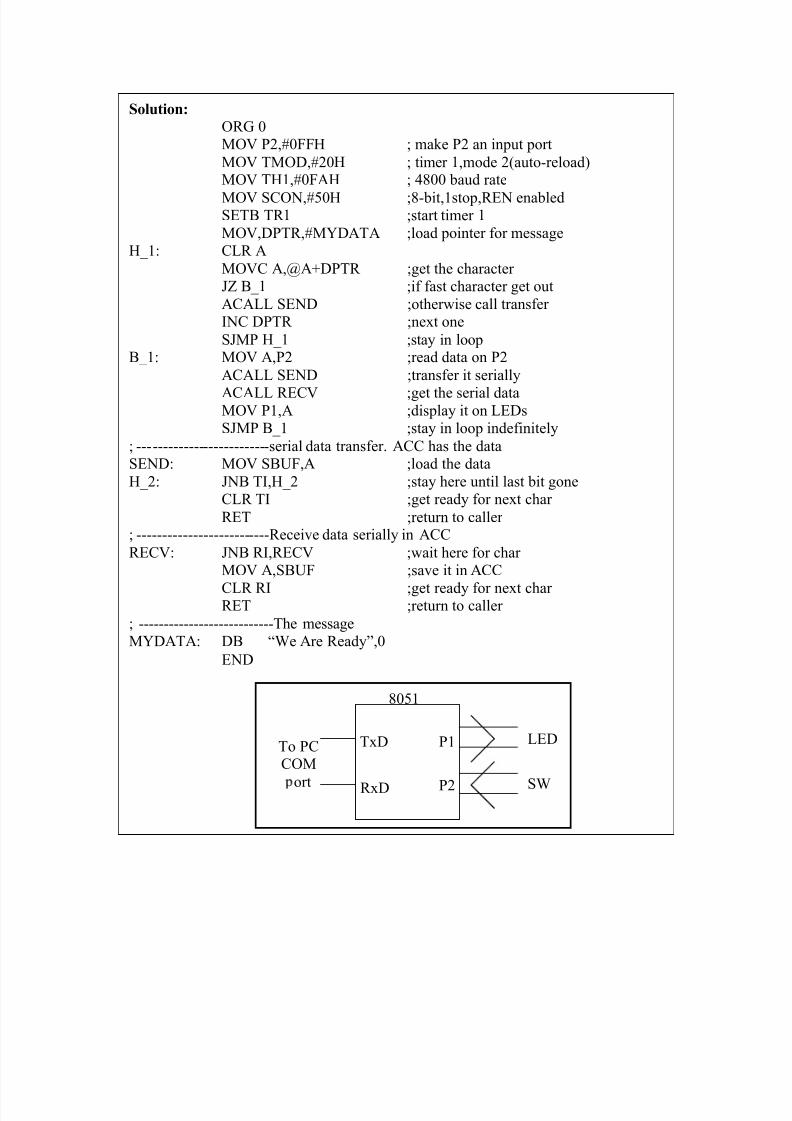
Solution:
ORG 0MOV P2,#0FFH ; make P2 an input port
MOV TMOD,#20H ; timer 1,mode 2(auto-reload)MOV TH1,#0FAH ; 4800 baud rate
MOV SCON,#50H ;8-bit,1stop,REN enabledSETB TR 1 ;start timer 1
MOV,DPTR,#MYDATA ;load pointer for messageH_1: CLR A
MOVC A,@A+DPTR ;get the character JZ B _1 ;if fast character get out
ACALL SEND ;otherwise call transfer INC DPTR ;next one
SJMP H_1 ;stay in loopB _1: MOV A,P2 ;read data on P2
ACALL SEND ;transfer it serially
ACALL RECV ;get the serial dataMOV P1,A ;display it on LEDsSJMP B _1 ;stay in loop indefinitely
; --------------------------serial data transfer. ACC has the dataSEND: MOV SBUF,A ;load the data
H_ 2: JNB TI,H_ 2 ;stay here until last bit goneCLR TI ;get ready for next char
RET ;return to caller ; --------------------------Receive data serially in ACC
RECV: JNB RI,RECV ;wait here for char MOV A,SBUF ;save it in ACC
CLR RI ;get ready for next char RET ;return to caller
; ---------------------------The messageMYDATA: DB ³We Are Ready´,0
END
TxD
RxD
P1
P2
8051
To PCCOM
ort
LED
SW
8/8/2019 ASSGMT 2
http://slidepdf.com/reader/full/assgmt-2 46/54
Importance of the RI flag bit
In receiving bits via its RxD pin, the 8051 goes trough the following steps.
1. It receives the start bit indicating that the next bit is the first bit of the character
byte it is about to receive.2. The 8-bit character is received one bit at time. When the last bit is received, a byteis formed and placed in SBUF.
3. The stop bit is received. It is during receiving the stop bit that the 8051 makes RI= 1, indicating that an entire character byte has been received and must be picked
up before it gets overwritten by an incoming character.4. By checking the RI flag bit when it is raised, we know that a character has been
received and is sitting in the SBUF register. We copy the SBUF contents to a safe place in some other register or memory before it is lost.
5. After the SBUF contents are copied into a safe place, the RI flag bit must beforced to 0 by the ³CLR RI´ instruction in order to allow the next received
character byte to be placed in SBUF. Failure to do this causes loss of the receivedcharacter.
From the above discussion we conclude that by checking the RI flag bit we know
whether or not the 8051 has received a character byte. If we fail to copy SBUF into a safe place, we risk the loss of the received byte. More importantly, it must be noted that the RI
flag bit is raised by the 8051, but it must be noted cleared by the programmer with aninstruction such as ³CLR TI´. It also must be noted that if we copy SBUF into a safe
place before the RI flag bit raised, we risk copying garbage. The RI flag bit can bechecked by the instruction ³JNB RI, xx´ or by using an interrupt, as we will see in
Chapter II.
8/8/2019 ASSGMT 2
http://slidepdf.com/reader/full/assgmt-2 47/54
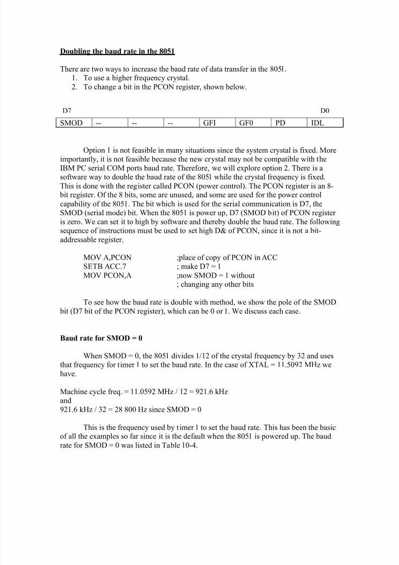
Doubling the baud rate in the 8051
There are two ways to increase the baud rate of data transfer in the 8051.1. To use a higher frequency crystal.
2. To change a bit in the PCON register, shown below.
SMOD -- -- -- GFI GF0 PD IDL
Option 1 is not feasible in many situations since the system crystal is fixed. Moreimportantly, it is not feasible because the new crystal may not be compatible with the
IBM PC serial COM ports baud rate. Therefore, we will explore option 2. There is asoftware way to double the baud rate of the 8051 while the crystal frequency is fixed.
This is done with the register called PCON (power control). The PCON register is an 8-
bit register. Of the 8 bits, some are unused, and some are used for the power controlcapability of the 8051. The bit which is used for the serial communication is D7, theSMOD (serial mode) bit. When the 8051 is power up, D7 (SMOD bit) of PCON register
is zero. We can set it to high by software and thereby double the baud rate. The followingsequence of instructions must be used to set high D& of PCON, since it is not a bit-
addressable register.
MOV A,PCON ;place of copy of PCON in ACCSETB ACC.7 ; make D7 = 1
MOV PCON,A ;now SMOD = 1 without; changing any other bits
To see how the baud rate is double with method, we show the pole of the SMOD
bit (D7 bit of the PCON register), which can be 0 or 1. We discuss each case.
Baud rate for SMOD = 0
When SMOD = 0, the 8051 divides 1/12 of the crystal frequency by 32 and usesthat frequency for timer 1 to set the baud rate. In the case of XTAL = 11.5092 MHz we
have.
Machine cycle freq. = 11.0592 MHz / 12 = 921.6 k Hzand
921.6 k Hz / 32 = 28 800 Hz since SMOD = 0
This is the frequency used by t imer 1 to set the baud rate. This has been the basicof all the examples so far since it is the default when the 8051 is powered up. The baud
rate for SMOD = 0 was listed in Table 10-4.
D7 D0

8/8/2019 ASSGMT 2
http://slidepdf.com/reader/full/assgmt-2 48/54
Baud rate for SMOD = 1
With the fixed crystal frequency, we can double the baud rate by making SMOD= 1. When the SMOD bit (D7 of the PCON register) is set to 1, 1/12 of XTAL is divided
by 16 (instead of 32) and that is the frequency used by timer 1 to set the baud rate. In the
case of XTAL = 11.0592 MHz, we have:
Machine cycle freq. = 11.0592 MHz / 12 = 921.6 k Hz
and921.6 k Hz / 16 = 57 600 Hz since SMOD
This is the frequency used by t imer 1 to set the baud rate.
Table 10-5 shows that the values loaded into THI are the same for both cases; however,the baud rates are doubles when SMOD = 1. Look at the following examples to clarify
the data given in table 10-5.
Table 10-5: Baud Rate Comparison for SMOD = 0 and SMOD = 1
TH1 (Decimal) (Hex) SMOD = 0 SMOD = 1
-3 FD 9 600 19 200
-6 FA 4 800 9 600
-12 F4 2 400 4 800
-24 E8 1 200 2 400
Note: XTAL = 11.0592 MHz
8/8/2019 ASSGMT 2
http://slidepdf.com/reader/full/assgmt-2 49/54
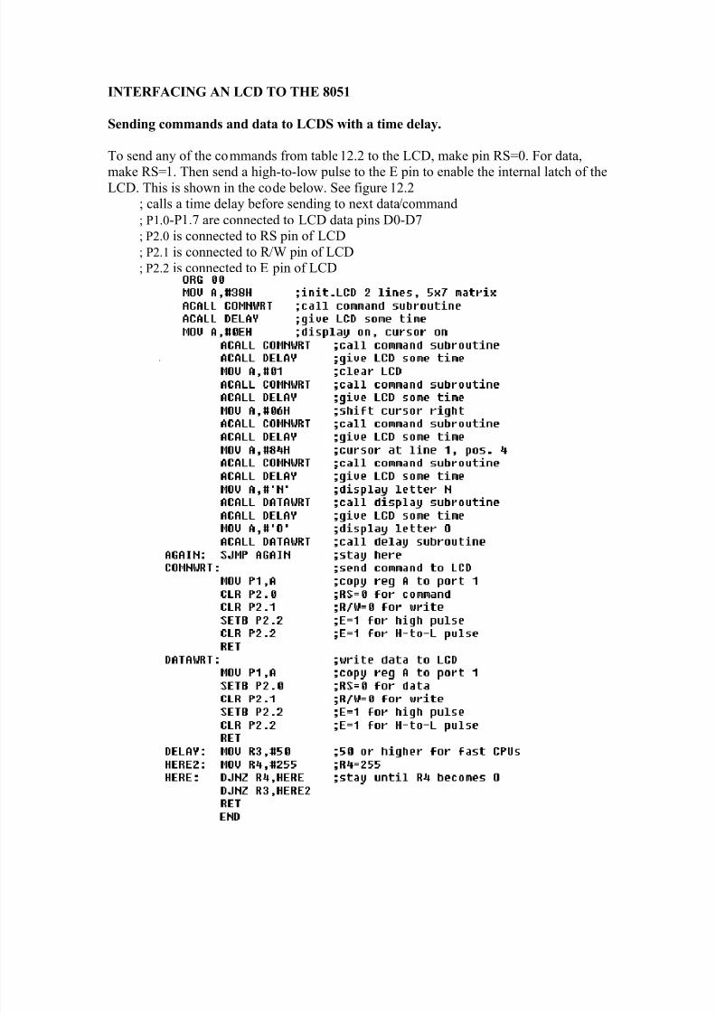
INTERFACING AN LCD TO THE 8051
Sending commands and data to LCDS with a time delay.
To send any of the commands from table 12.2 to the LCD, make pin RS=0. For data,
make RS=1. Then send a high-to-low pulse to the E pin to enable the internal latch of theLCD. This is shown in the code below. See figure 12.2; calls a time delay before sending to next data/command
; P1.0-P1.7 are connected to LCD data pins D0-D7; P2.0 is connected to RS pin of LCD
; P2.1 is connected to R /W pin of LCD; P2.2 is connected to E pin of LCD
8/8/2019 ASSGMT 2
http://slidepdf.com/reader/full/assgmt-2 50/54
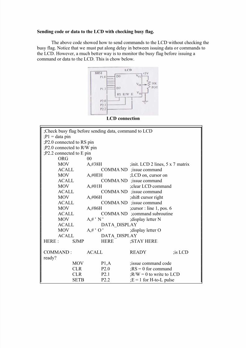
Sending code or data to the LCD with checking busy flag.
The above code showed how to send commands to the LCD without checking the busy flag. Notice that we must put along delay in between issuing data or commands to
the LCD. However, a much better way is to monitor the busy flag before issuing a
command or data to the LCD. This is chow below.
LCD connection
;Check busy flag before sending data, command to LCD
;P1 = data pin
;P2.0 connected to RS pin;P2.0 connected to R /W pin
;P2.2 connected to E pinORG 00
MOV A,#38H ;init. LCD 2 lines, 5 x 7 matrixACALL COMMA ND ;issue command
MOV A,#0EH ;LCD on, cursor on
ACALL COMMA ND ;issue commandMOV A,#01H ;clear LCD commandACALL COMMA ND ;issue command
MOV A,#06H ;shift cursor rightACALL COMMA ND ;issue command
MOV A,#86H ;cursor : line 1, pos. 6ACALL COMMA ND ;command subroutine
MOV A,# N ;display letter NACALL DATA_ DISPLAYMOV A,# O ;display letter O
ACALL DATA_ DISPLAYHERE : SJMP HERE ;STAY HERE
COMMA ND : ACALL READY ;is LCD
ready?MOV P1,A ;issue command code
CLR P2.0 ;RS = 0 for commandCLR P2.1 ;R /W = 0 to write to LCD
SETB P2.2 ;E = 1 for H-to-L pulse

8/8/2019 ASSGMT 2
http://slidepdf.com/reader/full/assgmt-2 51/54
Notice in the above program that the busy flag is D7 of the command register. Toread the command register we make R /W = 1 ,RS = 0 , and a H-to-L pulse for the E pin
will provide us the command register. After reading the command register, if bit D7 (the busy flag) is high, the LCD is busy and no information (command or data) should be
issued to it. Only when D7 = 0 can we send data or commands to the LCD. Notice in thismethod that there are no time delays used since we are checking the busy flag before
issuing commands or data to the LCD.
CLR P2.2 ;E = 0 latch in
RETDATA_ DISPLAY :
ACALL READY ;is LCD ready?MOV P1,A ;issue data
SETB P2,0 ;RS = 1 for data
CLR P2.1 ;R /W = 0 to write to LCDSETB P2.2 ;E = 1 for H-to-L pulseCLR P2.2 ;E= 0,latch in
READY :SETB P1.7 ;make P1.7 input port
CLR P2.0 ;RS=0 access command regSETB P2.1 ;R /W = 1 read command reg
;read command reg and check busy flagBACK: CLR P2.2 ;E=1 for H-to-L pulse
SETB P2.2 ;E=0 H-to-L pulseJB P1.7,BACK ;stay until busy flag = 0
RETEND
8/8/2019 ASSGMT 2
http://slidepdf.com/reader/full/assgmt-2 52/54
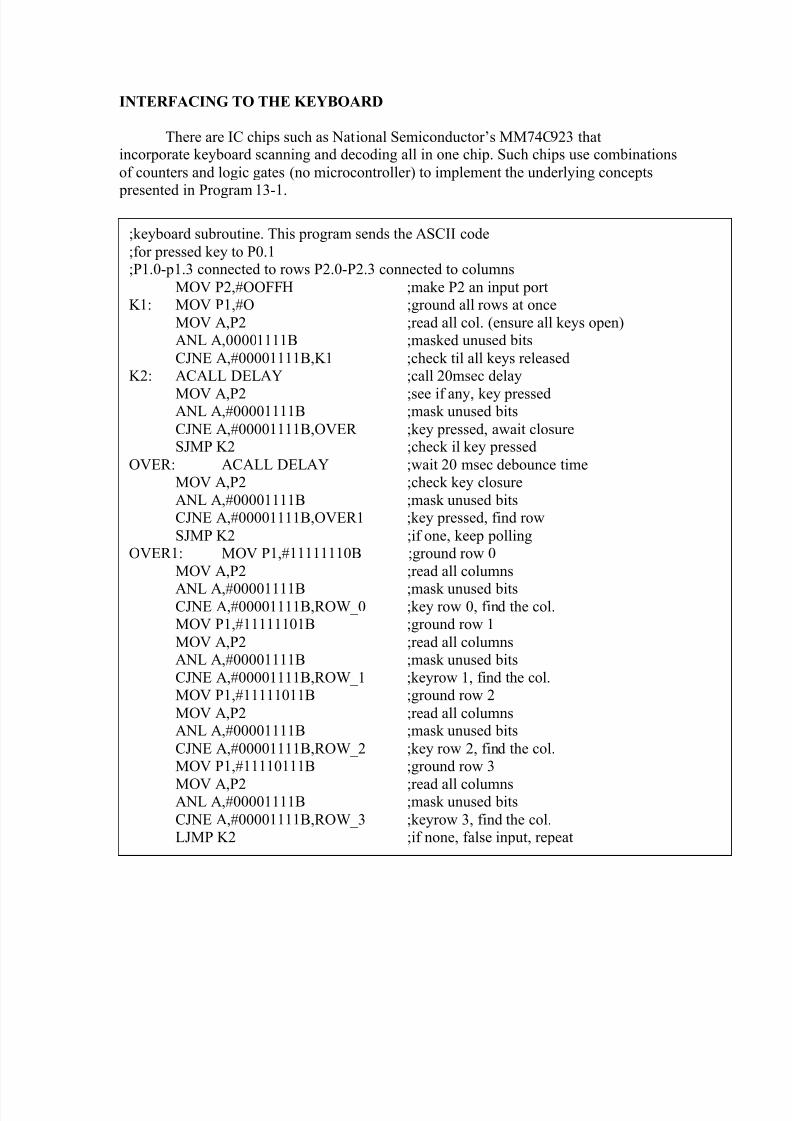
INTERFACING TO THE KEYBOARD
There are IC chips such as National Semiconductor¶s MM74C923 thatincorporate keyboard scanning and decoding all in one chip. Such chips use combinations
of counters and logic gates (no microcontroller) to implement the underlying concepts
presented in Program 13-1.
;keyboard subroutine. This program sends the ASCII code
;for pressed key to P0.1 ;P1.0-p1.3 connected to rows P2.0-P2.3 connected to columns
MOV P2,#OOFFH ;make P2 an input portK 1: MOV P1,#O ;ground all rows at once
MOV A,P2 ;read all col. (ensure all keys open)A NL A,00001111B ;masked unused bits
CJNE A,#00001111B,K 1 ;check til all keys releasedK2: ACALL DELAY ;call 20msec delay
MOV A,P2 ;see if any, key pressedA NL A,#00001111B ;mask unused bits
CJNE A,#00001111B,OVER ;key pressed, await closureSJMP K2 ;check il key pressed
OVER: ACALL DELAY ;wait 20 msec debounce timeMOV A,P2 ;check key closure
A NL A,#00001111B ;mask unused bitsCJNE A,#00001111B,OVER 1 ;key pressed, find row
SJMP K2 ;if one, keep pollingOVER 1: MOV P1,#11111110B ;ground row 0
MOV A,P2 ;read all columns
A NL A,#00001111B ;mask unused bitsCJNE A,#00001111B,ROW _ 0 ;key row 0, find the col.MOV P1,#11111101B ;ground row 1
MOV A,P2 ;read all columnsA NL A,#00001111B ;mask unused bits
CJNE A,#00001111B,ROW _1 ;keyrow 1, find the col.MOV P1,#11111011B ;ground row 2
MOV A,P2 ;read all columnsA NL A,#00001111B ;mask unused bits
CJNE A,#00001111B,ROW _ 2 ;key row 2, find the col.MOV P1,#11110111B ;ground row 3
MOV A,P2 ;read all columnsA NL A,#00001111B ;mask unused bits
CJNE A,#00001111B,ROW _ 3 ;keyrow 3, find the col.LJMP K2 ;if none, false input, repeat
8/8/2019 ASSGMT 2
http://slidepdf.com/reader/full/assgmt-2 53/54
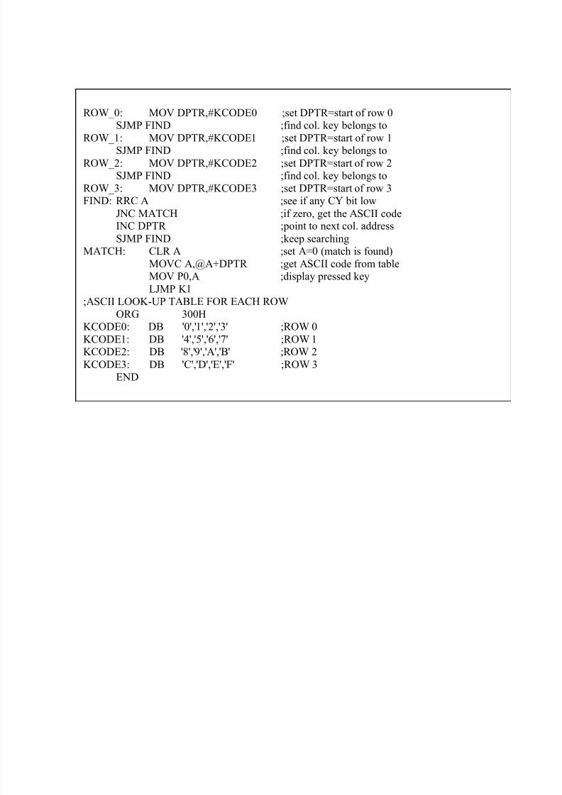
ROW _ 0: MOV DPTR,#KCODE0 ;set DPTR=start of row 0SJMP FIND ;find col. key belongs to
ROW _1: MOV DPTR,#KCODE1 ;set DPTR=start of row 1 SJMP FIND ;find col. key belongs to
ROW _ 2: MOV DPTR,#KCODE2 ;set DPTR=start of row 2SJMP FIND ;find col. key belongs to
ROW _ 3: MOV DPTR,#KCODE3 ;set DPTR=start of row 3FIND: RRC A ;see if any CY bit low
JNC MATCH ;if zero, get the ASCII codeINC DPTR ;point to next col. address
SJMP FIND ;keep searchingMATCH: CLR A ;set A=0 (match is found)
MOVC A,@A+DPTR ;get ASCII code from table
MOV P0,A ;display pressed keyLJMP K 1
;ASCII LOOK-UP TABLE FOR EACH ROW
ORG 300H KCODE0: DB '0','1','2','3' ;ROW 0
KCODE1: DB '4','5','6','7' ;ROW 1 KCODE2: DB '8','9','A','B' ;ROW 2
KCODE3: DB 'C','D','E','F' ;ROW 3END

8/8/2019 ASSGMT 2
http://slidepdf.com/reader/full/assgmt-2 54/54
Task 4: To test and simulate assembly language software using Kiel¶s 8051 IDEsoftware.
Answer: