ASIC1 progress Jamie Crooks, Feb 08. Bonding Problems: Resolved Smaller bonding wedge + revised...
13
ASIC1 progress Jamie Crooks, Feb 08
-
date post
22-Dec-2015 -
Category
Documents
-
view
213 -
download
0
Transcript of ASIC1 progress Jamie Crooks, Feb 08. Bonding Problems: Resolved Smaller bonding wedge + revised...

ASIC1
progress
Jamie Crooks, Feb 08

Bonding Problems: Resolved
Smaller bonding wedge + revised programShorts to seal ring discovered under bonds

Bonding Status
1 8th August 200712 +DPW RAL TD (optics lab) Threshold scan ok (some bumps, not completely normal)
9 19th November 200712 +DPW RAL TD (optics lab)
reworked with new bond program: shorts on pix/aco/dco power nets
1119th November 2007 8
12 +DPW IC reworked with new bond program: threshold scan ok
1519th November 2007 8
12 +DPW RAL TD (optics lab)
reworked with new bond program: (shapers bad; samplers good)
1619th November 2007 2 5 +DPW RAL TD (optics lab) reworked with new bond program: threshold scan ok
1719th November 2007 8
12 +DPW RAL TD (optics lab) reworked with new bond program: threshold scan ok
1919th November 2007
10
12 +DPW RAL TD (optics lab)
reworked with new bond program: threshold scan fails (no RE signals?)
22/1
18/1
29/1
29/1
1/2
22/1
22/1
Bonded # Status Wafer/Split Location Notes
(per diode)
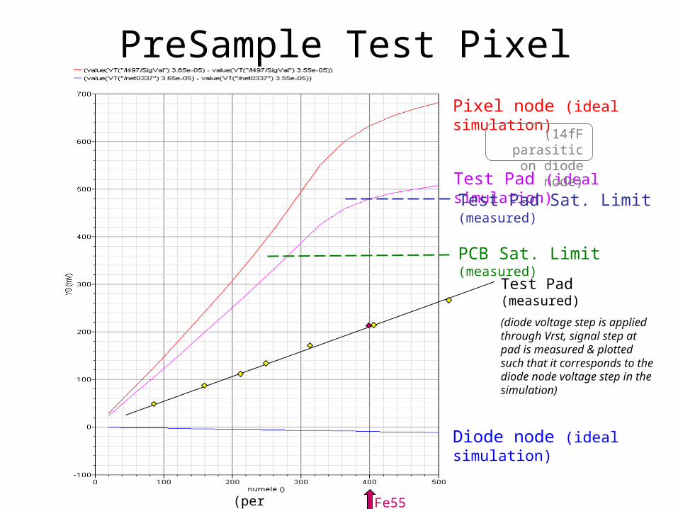
PreSample Test Pixel
Pixel node (ideal simulation)
Test Pad (ideal simulation)
PCB Sat. Limit (measured)
Diode node (ideal simulation)
Test Pad (measured)
(diode voltage step is applied through Vrst, signal step at pad is measured & plotted such that it corresponds to the diode node voltage step in the simulation)
Test Pad Sat. Limit (measured)
(14fF parasitic on diode node)
Fe55

System overview: preSample test pixels
Charge Gain (Diode) Voltage Gain (Electronics)
Q Vdiode Vpix Vpad
Voltage Gain (Buffers)
= 5.7 uV/e- (sim) (Can be estimated from ) Gain ~0.8 from simulations
Can be measured by applying Vstep to Vrst holding pixels in reset
Can be simulated by placing a voltage pulse on the diode node
Fe55 measurement should give calibration of this gain
Can be simulated using ideal or parasitic extracted pixel models and injecting charge

Voltage gainSimulation vs measured response: preSample test pixel
0
100
200
300
400
500
600
700
800
0 5 10 15 20 25 30
mV step applied to diode through Vrst
sig
na
l ste
p m
ag
nit
ud
e (
mV
)
Pixel schematicsimulation
Pixel Extractedsimulation
(Pixel signal:adjusted by 1/0.8gain factor from padmeasurements)
Measured padresponse
Simulations place an ideal voltage step on the diode node therefore independent of Cdiode
Measurements apply a voltage step on the diode node through the VRST transistor, therefore independent of Cdiode
62 V/V
24 V/V
31 V/V
Fe55

Compare with previous dataSimulation vs measured response: preSample test pixel
0
100
200
300
400
500
600
700
800
0 5 10 15 20 25 30
mV step applied to diode through Vrst
sig
na
l ste
p m
ag
nit
ud
e (
mV
)
Pixel schematicsimulation
Pixel Extractedsimulation
(Pixel signal: adjustedby 1/0.8 gain factorfrom padmeasurements)
Measured padresponse
PREVIOUS DATA:IDEAL SIM
PREVIOUS DATA:EXTRACTED SIM
PREVIOUS DATA:EXTRACTED PAD
Ass
um
ing
5.7
uV
/e-
con
vers
ion
Vrs
t st
ep

Measured voltage gain on 4 sensors
Different sensors: Voltage gain consistency check
0
50
100
150
200
250
300
350
400
450
0 5 10 15 20 25
mV step applied to Vrst
mV
ste
p m
easu
red
at
pad
& s
cop
e
pcb17
pcb17(scope)
pcb16
pcb16(scope)
pcb15
pcb16(scope)
pcb01

System overview: preSample test pixels
Charge Gain (Diode) Voltage Gain (Electronics)
Q Vdiode Vpix Vpad
Voltage Gain (Buffers)
These figures combined have been generally quoted before during design phase, in uV/e-
Any measurements taken with the test pixels will include the two buffer stages with gain<1
From Fe55 measurements = 130uV/e-
Est. from Fe55 meas. = 161uV/e-
= 5.7 uV/e- (sim)
= 31 V/V (est. from meas) = 0.8 V/V (sim)
= 24 V/V (measured) (136uV/e-)

Noise • Assumptions
– We are in the linear region of test pixel– Parasitic capacitance estimate of diode node is ~correct
• System gain– from diode to pad
• Noise – measured by Marcel at pad– referred back to diode using gain– Will be sampled in-pixel
during normal operation
• SNR– Typical signal– Worst case signal in corner
= 130uV/e-
= 3.5mV
207mV
1600e-
= 27 e-3.5mV
130uV/e
27 * √2 = 38 e-
250e- = 6.5

Linearity Measurements
0
50
100
150
200
250
300
350
400
450
0 20 40 60 80 100
Series1
Series2
Laser intensity (%)
Sig
nal (
mV
)
Q vs % laser intensity
-2
0
2
4
6
8
10
12
14
16
0 25 50 75 100
% Laser intensity
Q(fC
)
Giulio’s laser calibration Aug 07
Pixel saturation
Laser non-linearity
Series1 Sensor 1: 12um epi +DPW; (PCB modified for AC coupling)
Series2 Sensor 16: 5um epi +DPW(standard PCB design)

Linearity Sweeps
0
10
20
30
40
50
60
70
80
90
100
0 20 40 60 80 100 120
Series1
Series2
0
50
100
150
200
250
300
350
0 20 40 60 80 100 120
Series1
Series2
11x11 shutter
6x6 shutter
16x16 shutter
Non-linear region of laser

(Data from Jamie B)
• samplers with source • samplers without source • shapers with source• shapers without source
• histogram of the number of hits at each timestamp integrated over a very large number of bunch trains (~360k), for thresholds down to 160.