Applied Surface Science - Physics Main | Physics
6
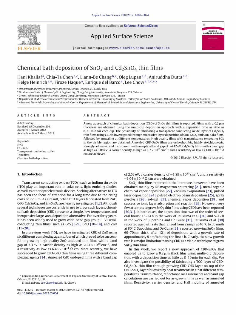
Applied Surface Science 258 (2012) 6069–6074 Contents lists available at SciVerse ScienceDirect Applied Surface Science j our nal ho me p age: www.elsevier.com/loc ate/apsusc Chemical bath deposition of SnO 2 and Cd 2 SnO 4 thin films Hani Khallaf a , Chia-Ta Chen b,c , Liann-Be Chang b,c , Oleg Lupan a,d , Aniruddha Dutta a,e , Helge Heinrich a,e , Firoze Haque a , Enrique del Barco a , Lee Chow a,b,c,e,∗ a Department of Physics, University of Central Florida, Orlando, FL 32816, USA b Graduate Institute of Electro-Optical Engineering, Chang Gung University, Kweishan, Taoyuan 333, Taiwan c Green Technology Research Center, Chang Gung University, Kweishan, Taoyuan 333, Taiwan d Department of Microelectronics and Semiconductor Devices, Technical University of Moldova, 168 Stefan cel Mare Boulevard, MD-2004 Chisinau, Republic of Moldova e Advanced Materials Processing and Analysis Centre, Department of Mechanical, Materials, and Aerospace Engineering, University of Central Florida, Orlando, FL 32816, USA a r t i c l e i n f o Article history: Received 15 December 2011 Accepted 1 March 2012 Available online 7 March 2012 Keywords: SnO2 Cd2SnO4 Transparent conducting oxides Thin films Chemical bath deposition a b s t r a c t A new approach of chemical bath deposition (CBD) of SnO 2 thin films is reported. Films with a 0.2 m thickness are obtained using the multi-dip deposition approach with a deposition time as little as 8–10 min for each dip. The possibility of fabricating a transparent conducting oxide layer of Cd 2 SnO 4 thin films using CBD is investigated through successive layer deposition of CBD-SnO 2 and CBD-CdO films, followed by annealing at different temperatures. High quality films with transmittance exceeding 80% in the visible region are obtained. Annealed CBD-SnO 2 films are orthorhombic, highly stoichiometric, strongly adhesive, and transparent with an optical band gap of ∼4.42 eV. Cd 2 SnO 4 films with a band gap as high as 3.08 eV; a carrier density as high as 1.7 × 10 20 cm −3 ; and a resistivity as low as 1.01 × 10 −2 cm are achieved. © 2012 Elsevier B.V. All rights reserved. 1. Introduction Transparent conducting oxides (TCOs) such as indium tin oxide (ITO) play an important role in solar cells, light emitting diodes, as well as other optoelectronic devices. Seeking alternatives to ITO has been the focus of attention for a long time due to the rising costs of indium. As a result, other TCO layers fabricated from ZnO, CdO, Cd 2 SnO 4 , and Zn 2 SnO 4 are heavily investigated [1,2]. Although several techniques are currently in use to grow such layers, chemi- cal bath deposition (CBD) presents a simple, low temperature, and inexpensive large-area deposition alternative. For over forty years, it has been widely used to grow wide-band gap group II–VI semi- conducting thin films, such as CdS [3–9], CdO [10–14], and ZnO [15–20]. In a previous work [15], we have investigated CBD of ZnO using six different complexing agents, four of which proved to be success- ful in growing high quality ZnO undoped thin films with a band gap of 3.3 eV, a carrier density as high as 2.24 × 10 19 cm −3 , and a resistivity as low as 6.48 × 10 −1 cm. More recently, we have succeeded to grow CBD-CdO thin films using three different com- plexing agents [14]. Annealed CdO undoped films with a band gap ∗ Corresponding author at: Department of Physics, University of Central Florida, Orlando, FL 32816, USA. E-mail address: [email protected] (L. Chow). of 2.53 eV, a carrier density of ∼1.89 × 10 20 cm −3 , and a resistivity ∼1.04 × 10 −2 cm were obtained. SnO 2 thin films reported in the literature, however, have been obtained mainly by RF magnetron sputtering [21], metal organic chemical vapor deposition [22], vacuum evaporation [23], pulsed laser deposition [24], pulsed electron beam deposition [25], spray pyrolysis [26], sol–gel [27], chemical vapor deposition [28], and successive ionic layer adsorption and reaction [29]. However, very few attempts to grow SnO 2 thin films using CBD have been reported [30,31]. In both cases, the deposition time was of the order of sev- eral hours; 15–24 h in the work of Tsukuma et al. [30] and 5–12 h in the work of Supothina and De Guire [31]. Tsukuma et al. [30] reported a growth rate that ranged from 2 nm/h at 40 ◦ C to 50 nm/h at 80 ◦ C. Supothina and De Guire [31] reported growing SnO 2 films, 60–70 nm thick, after 12 h of deposition, with a growth rate of approximately 9 nm/h during the first 4 h. Clearly, the slow growth rate is a major limitation to using CBD as a viable technique to grow SnO 2 thin films. In this work, we report a new approach of CBD-SnO 2 that enabled us to grow a 0.2 m thick film using multi-dip deposi- tion, with a deposition time as little as 8–10 min for each dip. We also investigate the possibility of fabricating a TCO layer of CBD- Cd 2 SnO 4 thin film through growing CBD-CdO layer on top of the CBD-SnO 2 layer followed by heat treatments in air at different tem- peratures. Transmittance, reflectance measurements and band gap calculations are carried out for as-grown films as well as annealed films. Resistivity, carrier density, and Hall mobility of annealed 0169-4332/$ – see front matter © 2012 Elsevier B.V. All rights reserved. doi:10.1016/j.apsusc.2012.03.004
Transcript of Applied Surface Science - Physics Main | Physics
C
HHa
b
c
d
e
a
ARAA
KSCTTC
1
(ahcCsciic[
sfgasp
O
0d
Applied Surface Science 258 (2012) 6069– 6074
Contents lists available at SciVerse ScienceDirect
Applied Surface Science
j our nal ho me p age: www.elsev ier .com/ loc ate /apsusc
hemical bath deposition of SnO2 and Cd2SnO4 thin films
ani Khallafa, Chia-Ta Chenb,c, Liann-Be Changb,c, Oleg Lupana,d, Aniruddha Duttaa,e,elge Heinricha,e, Firoze Haquea, Enrique del Barcoa, Lee Chowa,b,c,e,∗
Department of Physics, University of Central Florida, Orlando, FL 32816, USAGraduate Institute of Electro-Optical Engineering, Chang Gung University, Kweishan, Taoyuan 333, TaiwanGreen Technology Research Center, Chang Gung University, Kweishan, Taoyuan 333, TaiwanDepartment of Microelectronics and Semiconductor Devices, Technical University of Moldova, 168 Stefan cel Mare Boulevard, MD-2004 Chisinau, Republic of MoldovaAdvanced Materials Processing and Analysis Centre, Department of Mechanical, Materials, and Aerospace Engineering, University of Central Florida, Orlando, FL 32816, USA
r t i c l e i n f o
rticle history:eceived 15 December 2011ccepted 1 March 2012vailable online 7 March 2012
a b s t r a c t
A new approach of chemical bath deposition (CBD) of SnO2 thin films is reported. Films with a 0.2 �mthickness are obtained using the multi-dip deposition approach with a deposition time as little as8–10 min for each dip. The possibility of fabricating a transparent conducting oxide layer of Cd2SnO4
thin films using CBD is investigated through successive layer deposition of CBD-SnO2 and CBD-CdO films,
eywords:nO2
d2SnO4
ransparent conducting oxideshin films
followed by annealing at different temperatures. High quality films with transmittance exceeding 80%in the visible region are obtained. Annealed CBD-SnO2 films are orthorhombic, highly stoichiometric,strongly adhesive, and transparent with an optical band gap of ∼4.42 eV. Cd2SnO4 films with a band gapas high as 3.08 eV; a carrier density as high as 1.7 × 1020 cm−3; and a resistivity as low as 1.01 × 10⁻² �cm are achieved.
hemical bath deposition
. Introduction
Transparent conducting oxides (TCOs) such as indium tin oxideITO) play an important role in solar cells, light emitting diodes,s well as other optoelectronic devices. Seeking alternatives to ITOas been the focus of attention for a long time due to the risingosts of indium. As a result, other TCO layers fabricated from ZnO,dO, Cd2SnO4, and Zn2SnO4 are heavily investigated [1,2]. Althougheveral techniques are currently in use to grow such layers, chemi-al bath deposition (CBD) presents a simple, low temperature, andnexpensive large-area deposition alternative. For over forty years,t has been widely used to grow wide-band gap group II–VI semi-onducting thin films, such as CdS [3–9], CdO [10–14], and ZnO15–20].
In a previous work [15], we have investigated CBD of ZnO usingix different complexing agents, four of which proved to be success-ul in growing high quality ZnO undoped thin films with a bandap of 3.3 eV, a carrier density as high as 2.24 × 1019 cm−3, and
resistivity as low as 6.48 × 10⁻¹ � cm. More recently, we have
ucceeded to grow CBD-CdO thin films using three different com-lexing agents [14]. Annealed CdO undoped films with a band gap∗ Corresponding author at: Department of Physics, University of Central Florida,rlando, FL 32816, USA.
E-mail address: [email protected] (L. Chow).
169-4332/$ – see front matter © 2012 Elsevier B.V. All rights reserved.oi:10.1016/j.apsusc.2012.03.004
© 2012 Elsevier B.V. All rights reserved.
of 2.53 eV, a carrier density of ∼1.89 × 1020 cm−3, and a resistivity∼1.04 × 10⁻² � cm were obtained.
SnO2 thin films reported in the literature, however, have beenobtained mainly by RF magnetron sputtering [21], metal organicchemical vapor deposition [22], vacuum evaporation [23], pulsedlaser deposition [24], pulsed electron beam deposition [25], spraypyrolysis [26], sol–gel [27], chemical vapor deposition [28], andsuccessive ionic layer adsorption and reaction [29]. However, veryfew attempts to grow SnO2 thin films using CBD have been reported[30,31]. In both cases, the deposition time was of the order of sev-eral hours; 15–24 h in the work of Tsukuma et al. [30] and 5–12 hin the work of Supothina and De Guire [31]. Tsukuma et al. [30]reported a growth rate that ranged from 2 nm/h at 40 ◦C to 50 nm/hat 80 ◦C. Supothina and De Guire [31] reported growing SnO2 films,60–70 nm thick, after 12 h of deposition, with a growth rate ofapproximately 9 nm/h during the first 4 h. Clearly, the slow growthrate is a major limitation to using CBD as a viable technique to growSnO2 thin films.
In this work, we report a new approach of CBD-SnO2 thatenabled us to grow a 0.2 �m thick film using multi-dip deposi-tion, with a deposition time as little as 8–10 min for each dip. Wealso investigate the possibility of fabricating a TCO layer of CBD-Cd2SnO4 thin film through growing CBD-CdO layer on top of the
CBD-SnO2 layer followed by heat treatments in air at different tem-peratures. Transmittance, reflectance measurements and band gapcalculations are carried out for as-grown films as well as annealedfilms. Resistivity, carrier density, and Hall mobility of annealed
6 ace Science 258 (2012) 6069– 6074
fisfietossr
2
cdsSat[sbTgwu
llfiaae
tCuit[
T
w
e
˛
wtdetepHHr�2wapwoa
070 H. Khallaf et al. / Applied Surf
lms are acquired at room temperatures using Hall effect mea-urements. Crystal structure as well as crystal quality of CBD-SnO2lms are determined using X-ray diffraction (XRD), transmissionlectron microscopy (TEM), and Fourier transform infrared spec-roscopy (FTIR). Film morphology, composition, and binding energyf CBD-SnO2 are studied using atomic force microscopy (AFM) andcanning electron microscopy (SEM), Rutherford backscatteringpectroscopy (RBS), and X-ray photoelectron spectroscopy (XPS),espectively.
. Experimental details
SnO2 films were prepared using aqueous solutions of tinhloride pentahydrate (0.028 M). Each bath contained 120 ml ofe-ionized water (resistivity ∼18.2 M�-cm) that was kept undertirring at 55 ◦C. Films were grown on 38 mm × 38 mm × 1 mmchott Borofloat glass as well as quartz substrates. With the help of
Teflon holder, the glass substrate was kept vertically in the solu-ion. The cleaning steps of the substrate are reported elsewhere6]. To ensure deposition of high-quality and adhesive films, theubstrate was removed from the solution whenever the solutionecomes turbid and the homogeneous reaction starts to take place.he deposition time was about 8–10 min for each dip. In order torow SnO2 films with a ∼0.2 �m thickness, the deposition processas repeated four consecutive times, with fresh solutions beingsed every time.
After annealing the SnO2 film at 400 ◦C in air for 1 h, a 0.2 �mayer of CdO is grown on top of the SnO2 layer using CBD. Bothayers are then annealed at different temperatures in air. CdO thinlms are grown using ammonia and ethanolamine as complexinggents, CdSO4 as cadmium source (NH4)2SO4 as a buffer, and H2O2s an oxidation agent. Details of CBD of CdO thin films are reportedlsewhere [14].
Specular transmittance measurements were carried out at roomemperature in the wavelength range from 200 to 1200 nm, using aary 500 (Varian) double beam UV/vis spectrophotometer. Spec-lar reflectance measurements were performed at an angle of
ncidence of 7◦ in the same wavelength range. The optical absorp-ion coefficient ̨ was calculated for each film using the equation32]:
= (1 − R)2 exp(−˛t) (1)
here T is transmittance, R is reflectance, and t is film thickness.The absorption coefficient ˛ is related to the incident photon
nergy h� as:
= K(h� − Eg)n/2
h�(2)
here K is a constant, Eg is the optical band gap, and n is equalo 1 for direct band gap material such as CdO. The band gap wasetermined for each film by plotting (˛h�)2 versus h� and thenxtrapolating the straight line portion to the energy axis. Resis-ivity, Hall mobility, and carrier density were evaluated by Hallffect measurements at room temperature in a Van der Pauw four-oint probe configuration, using indium contacts, in an automatedall effect system (Ecopia HMS-3000, Bridge Technology, Chandlereights AZ, USA) with a 0.55 T magnetic induction. XRD was car-
ied out using Rigaku D XRD unit (with 40 kV, 30 mA CuK� radiation, = 0.15406 nm). The sample was mounted at 2.5◦ and scanned from0◦ to 80◦ in steps of 0.02◦ with a scan rate of 1.2◦ min−1. TEMas performed using a Tecnai F30 STEM system operating at an
cceleration voltage of 300 kV. Cross sections of CdO films were
repared with FEI 200 focused ion beam system. SEM micrographsere obtained using a JEOL 6400F SEM at an acceleration voltagef 10 kV. The FTIR micro-analysis was performed at room temper-ture using contact ATR optimized objective that covers a range
Fig. 1. Specular transmittance of as-grown and annealed SnO2 films as well asCd2SnO4 films annealed at 200–600 ◦C.
of wavenumbers from 650 cm−1 to 4000 cm−1. RBS measurementswere acquired using a 2.25 MeV �-particles IONIX 1.7 MU Tande-tron, with a surface barrier detector with energy resolution ≤15 keV(full width at half maximum – FWHM), positioned at a scatteringangle of 165◦. XPS was performed on a Physical Electronics PHI5400 ESCA using unmonochromated Mg K� radiation at 1253.6 eV.Each of the XPS spectra was acquired from 30 repeated sweeps.XPS Spectra were corrected from charging effects by referencingthe adventitious C 1s peak to 284.6 eV. AFM images were acquiredusing Veeco Multimode SPM in tapping mode.
3. Results and discussion
It was observed that as-grown SnO2 films are extremely adhe-sive, where highly concentrated sulfuric acid (98%) and nitric acid(96%) could not etch them. Therefore, in order to perform opti-cal measurements, two substrates were tightly mounted togetheron the Teflon sample holder to ensure deposition on only oneside of the substrate. Film thickness was determined using TEM,as will be shown later. Fig. 1 shows the optical transmittance ofas-grown and annealed SnO2 films as well as CdO + SnO2 filmsannealed at 200, 300, 400, 500 and 600 ◦C. As shown, all filmsexhibit high transmittance that, in most cases, exceeds 80% in thevisible region. A red shift in the optical absorption edge is observeddue to formation of Cd2SnO4, which increases with increasingannealing temperature. The sharp absorption edge observed inCd2SnO4 layers indicates that films still maintain high quality, evenafter annealing at temperatures as high as 600 ◦C. Films annealedat higher temperatures did not maintain the same quality and werediscarded from any further characterizations. We have previouslyreported similar thermal-induced degradation of some CBD-ZnOand CBD-CdO films [14,15] that was attributed to stress in as-grownlayers which caused films to lose their integrity after annealing,even at temperatures as low as 200–300 ◦C [15]. Since SnO2 filmsinitially annealed at 400 ◦C maintained their integrity as will beshown later in this work, it is likely that the CdO top-layer is respon-sible for this degradation. However, because CBD-SnO2 films grownin this work were not separately subjected to heat treatments at
◦
temperatures higher than 400 C, we cannot rule out the possibilityof thermal-induced degradation of this layer at higher tempera-tures. Furthermore, growing CdO layer on top of SnO2 using CBDtypically exposes the SnO2 film to a high pH environment due to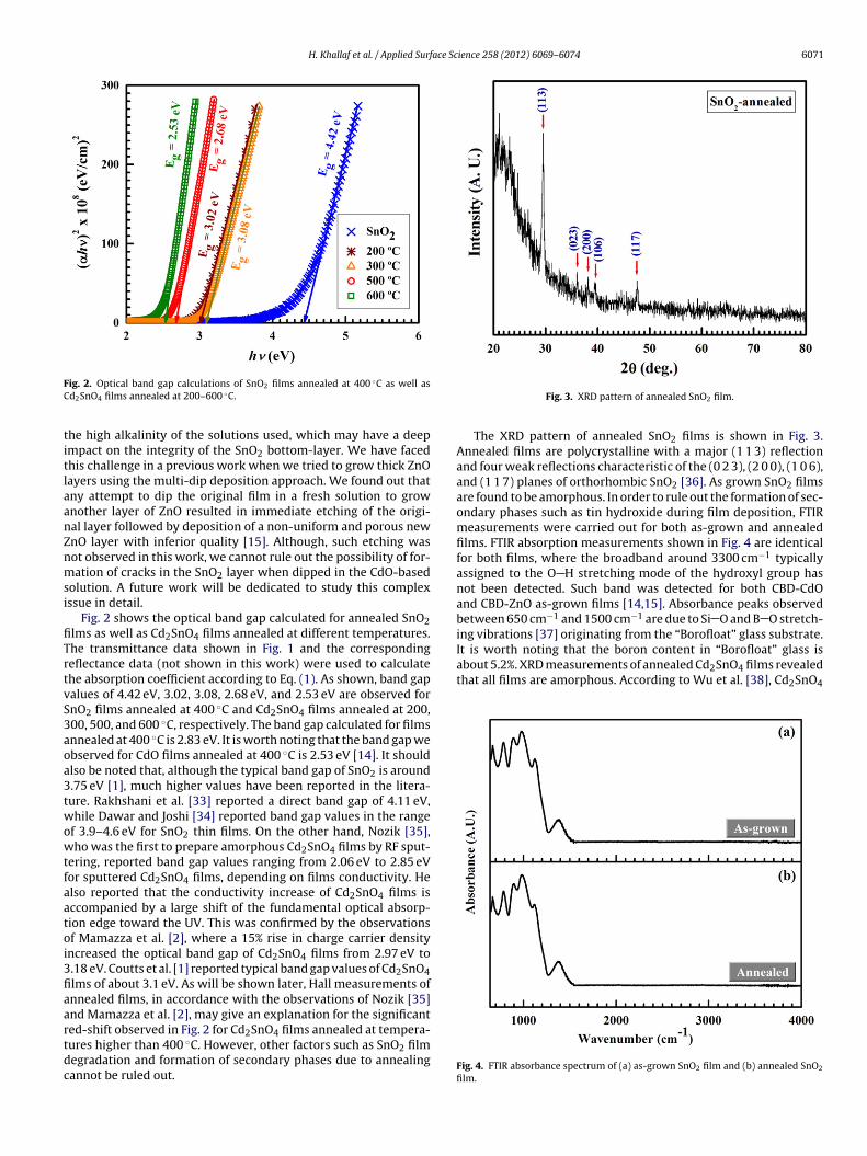
H. Khallaf et al. / Applied Surface Science 258 (2012) 6069– 6074 6071
FC
titlaanZnmsi
fiTrtvS3aoa3twowtfaatoi3fiaartdc
It is worth noting that the boron content in “Borofloat” glass isabout 5.2%. XRD measurements of annealed Cd2SnO4 films revealedthat all films are amorphous. According to Wu et al. [38], Cd2SnO4
ig. 2. Optical band gap calculations of SnO2 films annealed at 400 ◦C as well asd2SnO4 films annealed at 200–600 ◦C.
he high alkalinity of the solutions used, which may have a deepmpact on the integrity of the SnO2 bottom-layer. We have facedhis challenge in a previous work when we tried to grow thick ZnOayers using the multi-dip deposition approach. We found out thatny attempt to dip the original film in a fresh solution to grownother layer of ZnO resulted in immediate etching of the origi-al layer followed by deposition of a non-uniform and porous newnO layer with inferior quality [15]. Although, such etching wasot observed in this work, we cannot rule out the possibility of for-ation of cracks in the SnO2 layer when dipped in the CdO-based
olution. A future work will be dedicated to study this complexssue in detail.
Fig. 2 shows the optical band gap calculated for annealed SnO2lms as well as Cd2SnO4 films annealed at different temperatures.he transmittance data shown in Fig. 1 and the correspondingeflectance data (not shown in this work) were used to calculatehe absorption coefficient according to Eq. (1). As shown, band gapalues of 4.42 eV, 3.02, 3.08, 2.68 eV, and 2.53 eV are observed fornO2 films annealed at 400 ◦C and Cd2SnO4 films annealed at 200,00, 500, and 600 ◦C, respectively. The band gap calculated for filmsnnealed at 400 ◦C is 2.83 eV. It is worth noting that the band gap webserved for CdO films annealed at 400 ◦C is 2.53 eV [14]. It shouldlso be noted that, although the typical band gap of SnO2 is around.75 eV [1], much higher values have been reported in the litera-ure. Rakhshani et al. [33] reported a direct band gap of 4.11 eV,hile Dawar and Joshi [34] reported band gap values in the range
f 3.9–4.6 eV for SnO2 thin films. On the other hand, Nozik [35],ho was the first to prepare amorphous Cd2SnO4 films by RF sput-
ering, reported band gap values ranging from 2.06 eV to 2.85 eVor sputtered Cd2SnO4 films, depending on films conductivity. Helso reported that the conductivity increase of Cd2SnO4 films isccompanied by a large shift of the fundamental optical absorp-ion edge toward the UV. This was confirmed by the observationsf Mamazza et al. [2], where a 15% rise in charge carrier densityncreased the optical band gap of Cd2SnO4 films from 2.97 eV to.18 eV. Coutts et al. [1] reported typical band gap values of Cd2SnO4lms of about 3.1 eV. As will be shown later, Hall measurements ofnnealed films, in accordance with the observations of Nozik [35]nd Mamazza et al. [2], may give an explanation for the significant
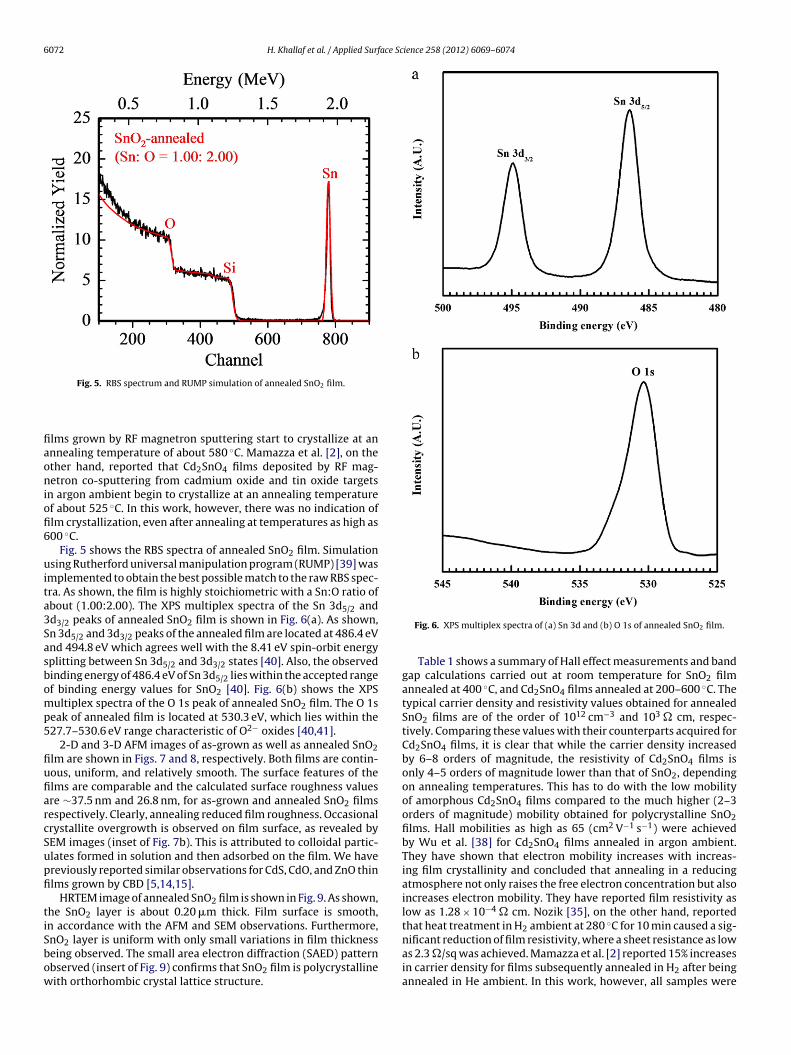
ed-shift observed in Fig. 2 for Cd2SnO4 films annealed at tempera-ures higher than 400 ◦C. However, other factors such as SnO2 filmegradation and formation of secondary phases due to annealingannot be ruled out.Fig. 3. XRD pattern of annealed SnO2 film.
The XRD pattern of annealed SnO2 films is shown in Fig. 3.Annealed films are polycrystalline with a major (1 1 3) reflectionand four weak reflections characteristic of the (0 2 3), (2 0 0), (1 0 6),and (1 1 7) planes of orthorhombic SnO2 [36]. As grown SnO2 filmsare found to be amorphous. In order to rule out the formation of sec-ondary phases such as tin hydroxide during film deposition, FTIRmeasurements were carried out for both as-grown and annealedfilms. FTIR absorption measurements shown in Fig. 4 are identicalfor both films, where the broadband around 3300 cm−1 typicallyassigned to the O H stretching mode of the hydroxyl group hasnot been detected. Such band was detected for both CBD-CdOand CBD-ZnO as-grown films [14,15]. Absorbance peaks observedbetween 650 cm−1 and 1500 cm−1 are due to Si O and B O stretch-ing vibrations [37] originating from the “Borofloat” glass substrate.
Fig. 4. FTIR absorbance spectrum of (a) as-grown SnO2 film and (b) annealed SnO2
film.
6072 H. Khallaf et al. / Applied Surface Science 258 (2012) 6069– 6074
fiaoniofi6
uita3Sasbomp5
fiufiarcSupfi
tiSbow
nificant reduction of film resistivity, where a sheet resistance as lowas 2.3 �/sq was achieved. Mamazza et al. [2] reported 15% increases
Fig. 5. RBS spectrum and RUMP simulation of annealed SnO2 film.
lms grown by RF magnetron sputtering start to crystallize at annnealing temperature of about 580 ◦C. Mamazza et al. [2], on thether hand, reported that Cd2SnO4 films deposited by RF mag-etron co-sputtering from cadmium oxide and tin oxide targets
n argon ambient begin to crystallize at an annealing temperaturef about 525 ◦C. In this work, however, there was no indication oflm crystallization, even after annealing at temperatures as high as00 ◦C.
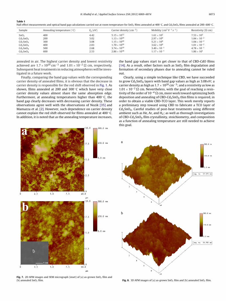
Fig. 5 shows the RBS spectra of annealed SnO2 film. Simulationsing Rutherford universal manipulation program (RUMP) [39] was
mplemented to obtain the best possible match to the raw RBS spec-ra. As shown, the film is highly stoichiometric with a Sn:O ratio ofbout (1.00:2.00). The XPS multiplex spectra of the Sn 3d5/2 andd3/2 peaks of annealed SnO2 film is shown in Fig. 6(a). As shown,n 3d5/2 and 3d3/2 peaks of the annealed film are located at 486.4 eVnd 494.8 eV which agrees well with the 8.41 eV spin-orbit energyplitting between Sn 3d5/2 and 3d3/2 states [40]. Also, the observedinding energy of 486.4 eV of Sn 3d5/2 lies within the accepted rangef binding energy values for SnO2 [40]. Fig. 6(b) shows the XPSultiplex spectra of the O 1s peak of annealed SnO2 film. The O 1s
eak of annealed film is located at 530.3 eV, which lies within the27.7–530.6 eV range characteristic of O2− oxides [40,41].
2-D and 3-D AFM images of as-grown as well as annealed SnO2lm are shown in Figs. 7 and 8, respectively. Both films are contin-ous, uniform, and relatively smooth. The surface features of thelms are comparable and the calculated surface roughness valuesre ∼37.5 nm and 26.8 nm, for as-grown and annealed SnO2 filmsespectively. Clearly, annealing reduced film roughness. Occasionalrystallite overgrowth is observed on film surface, as revealed byEM images (inset of Fig. 7b). This is attributed to colloidal partic-lates formed in solution and then adsorbed on the film. We havereviously reported similar observations for CdS, CdO, and ZnO thinlms grown by CBD [5,14,15].
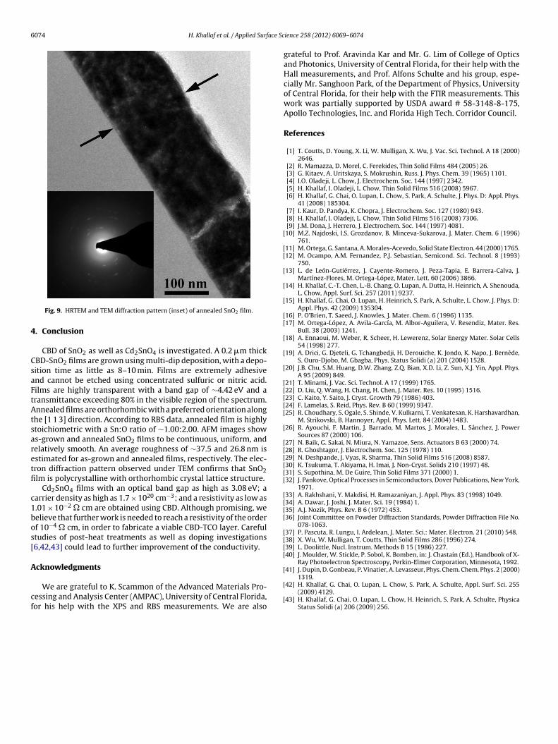
HRTEM image of annealed SnO2 film is shown in Fig. 9. As shown,he SnO2 layer is about 0.20 �m thick. Film surface is smooth,n accordance with the AFM and SEM observations. Furthermore,nO2 layer is uniform with only small variations in film thicknesseing observed. The small area electron diffraction (SAED) pattern
bserved (insert of Fig. 9) confirms that SnO2 film is polycrystallineith orthorhombic crystal lattice structure.Fig. 6. XPS multiplex spectra of (a) Sn 3d and (b) O 1s of annealed SnO2 film.
Table 1 shows a summary of Hall effect measurements and bandgap calculations carried out at room temperature for SnO2 filmannealed at 400 ◦C, and Cd2SnO4 films annealed at 200–600 ◦C. Thetypical carrier density and resistivity values obtained for annealedSnO2 films are of the order of 1012 cm−3 and 103 � cm, respec-tively. Comparing these values with their counterparts acquired forCd2SnO4 films, it is clear that while the carrier density increasedby 6–8 orders of magnitude, the resistivity of Cd2SnO4 films isonly 4–5 orders of magnitude lower than that of SnO2, dependingon annealing temperatures. This has to do with the low mobilityof amorphous Cd2SnO4 films compared to the much higher (2–3orders of magnitude) mobility obtained for polycrystalline SnO2films. Hall mobilities as high as 65 (cm2 V−1 s−1) were achievedby Wu et al. [38] for Cd2SnO4 films annealed in argon ambient.They have shown that electron mobility increases with increas-ing film crystallinity and concluded that annealing in a reducingatmosphere not only raises the free electron concentration but alsoincreases electron mobility. They have reported film resistivity aslow as 1.28 × 10⁻⁴ � cm. Nozik [35], on the other hand, reportedthat heat treatment in H2 ambient at 280 ◦C for 10 min caused a sig-
in carrier density for films subsequently annealed in H2 after beingannealed in He ambient. In this work, however, all samples were
H. Khallaf et al. / Applied Surface Science 258 (2012) 6069– 6074 6073
Table 1Hall effect measurements and optical band gap calculations carried out at room temperature for SnO2 films annealed at 400 ◦C, and Cd2SnO4 films annealed at 200–600 ◦C.
Sample Annealing temperature (◦C) Eg (eV) Carrier density (cm−3) Mobility (cm2 V−1 s−1) Resistivity (� cm)
SnO2 400 4.42 5.15 × 10¹² 1.61 × 10² 7.53 × 10³
Cd2SnO4 200 3.02 1.13 × 10²⁰ 2.97 × 100 1.84 × 10⁻²
Cd2SnO4 300 3.08 1.15 × 10²⁰ 5.21 × 100 1.04 × 10⁻²
.70 ×
20 0 −2
.74 ×
.86 ×
aaSt
ccscFboMcI
F(
Cd2SnO4 400 2.83 1Cd2SnO4 500 2.68 3Cd2SnO4 600 2.53 2
nnealed in air. The highest carrier density and lowest resistivitychieved are 1.7 × 1020 cm−3 and 1.01 × 10⁻² � cm, respectively.ubsequent heat treatments in reducing atmospheres will be inves-igated in a future work.
Finally, comparing the band gap values with the correspondingarrier density of annealed films, it is obvious that the decrease inarrier density is responsible for the red shift observed in Fig. 1. Ashown, films annealed at 200 and 300 ◦C which have very closearrier density values almost share the same absorption edge.urthermore, at annealing temperatures higher than 400 ◦C, theand gap clearly decreases with decreasing carrier density. These
bservations agree well with the observations of Nozik [35] andamazza et al. [2]. However, such dependence on carrier densityannot explain the red shift observed for films annealed at 400 ◦C.n addition, it is noted that as the annealing temperature increases,
ig. 7. 2D AFM images and SEM micrograph (inset) of (a) as-grown SnO2 film andb) annealed SnO2 film.
10 3.62 × 10 1.01 × 101019 3.49 × 10⁻¹ 4.78 × 10⁻¹
1018 1.17 × 10⁻¹ 1.86 × 101
the band gap values start to get closer to that of CBD-CdO films[14]. As a result, other factors such as SnO2 film degradation andformation of secondary phases due to annealing cannot be ruledout.
Clearly, using a simple technique like CBD, we have succeededto grow Cd2SnO4 layers with band gap values as high as 3.08 eV; acarrier density as high as 1.7 × 1020 cm−3; and a resistivity as low as1.01 × 10−2 � cm. Nevertheless, with the goal of reaching a resis-tivity of the order of 10−4 � cm, more work toward optimizing bothdeposition and annealing of CBD-Cd2SnO4 thin films is required, inorder to obtain a viable CBD-TCO layer. This work merely reportsa preliminary step toward using CBD to fabricate a TCO layer ofCd2SnO4. Careful studies of post-heat treatments using differentambient such as He, Ar, and H2; as well as thorough investigationsof CBD-Cd2SnO4 film crystallinity, stoichiometry, and composition
as a function of annealing temperature are still needed to achievethis goal.Fig. 8. 3D AFM images of (a) as-grown SnO2 film and (b) annealed SnO2 film.
6074 H. Khallaf et al. / Applied Surface Sc
4
CsaFtAtsaretfi
c1bos[
A
cf
[
[[
[
[
[
[[
[
[
[
[[[[[
[
[[[[[[
[[[[
[[[[
[
Fig. 9. HRTEM and TEM diffraction pattern (inset) of annealed SnO2 film.
. Conclusion
CBD of SnO2 as well as Cd2SnO4 is investigated. A 0.2 �m thickBD-SnO2 films are grown using multi-dip deposition, with a depo-ition time as little as 8–10 min. Films are extremely adhesivend cannot be etched using concentrated sulfuric or nitric acid.ilms are highly transparent with a band gap of ∼4.42 eV and aransmittance exceeding 80% in the visible region of the spectrum.nnealed films are orthorhombic with a preferred orientation along
he [1 1 3] direction. According to RBS data, annealed film is highlytoichiometric with a Sn:O ratio of ∼1.00:2.00. AFM images shows-grown and annealed SnO2 films to be continuous, uniform, andelatively smooth. An average roughness of ∼37.5 and 26.8 nm isstimated for as-grown and annealed films, respectively. The elec-ron diffraction pattern observed under TEM confirms that SnO2lm is polycrystalline with orthorhombic crystal lattice structure.
Cd2SnO4 films with an optical band gap as high as 3.08 eV; aarrier density as high as 1.7 × 1020 cm−3; and a resistivity as low as.01 × 10−2 � cm are obtained using CBD. Although promising, weelieve that further work is needed to reach a resistivity of the orderf 10−4 � cm, in order to fabricate a viable CBD-TCO layer. Carefultudies of post-heat treatments as well as doping investigations6,42,43] could lead to further improvement of the conductivity.
cknowledgments
We are grateful to K. Scammon of the Advanced Materials Pro-essing and Analysis Center (AMPAC), University of Central Florida,or his help with the XPS and RBS measurements. We are also
[
[
ience 258 (2012) 6069– 6074
grateful to Prof. Aravinda Kar and Mr. G. Lim of College of Opticsand Photonics, University of Central Florida, for their help with theHall measurements, and Prof. Alfons Schulte and his group, espe-cially Mr. Sanghoon Park, of the Department of Physics, Universityof Central Florida, for their help with the FTIR measurements. Thiswork was partially supported by USDA award # 58-3148-8-175,Apollo Technologies, Inc. and Florida High Tech. Corridor Council.
References
[1] T. Coutts, D. Young, X. Li, W. Mulligan, X. Wu, J. Vac. Sci. Technol. A 18 (2000)2646.
[2] R. Mamazza, D. Morel, C. Ferekides, Thin Solid Films 484 (2005) 26.[3] G. Kitaev, A. Uritskaya, S. Mokrushin, Russ. J. Phys. Chem. 39 (1965) 1101.[4] I.O. Oladeji, L. Chow, J. Electrochem. Soc. 144 (1997) 2342.[5] H. Khallaf, I. Oladeji, L. Chow, Thin Solid Films 516 (2008) 5967.[6] H. Khallaf, G. Chai, O. Lupan, L. Chow, S. Park, A. Schulte, J. Phys. D: Appl. Phys.
41 (2008) 185304.[7] I. Kaur, D. Pandya, K. Chopra, J. Electrochem. Soc. 127 (1980) 943.[8] H. Khallaf, I. Oladeji, L. Chow, Thin Solid Films 516 (2008) 7306.[9] J.M. Dona, J. Herrero, J. Electrochem. Soc. 144 (1997) 4081.10] M.Z. Najdoski, I.S. Grozdanov, B. Minceva-Sukarova, J. Mater. Chem. 6 (1996)
761.11] M. Ortega, G. Santana, A. Morales-Acevedo, Solid State Electron. 44 (2000) 1765.12] M. Ocampo, A.M. Fernandez, P.J. Sebastian, Semicond. Sci. Technol. 8 (1993)
750.13] L. de León-Gutiérrez, J. Cayente-Romero, J. Peza-Tapia, E. Barrera-Calva, J.
Martínez-Flores, M. Ortega-López, Mater. Lett. 60 (2006) 3866.14] H. Khallaf, C.-T. Chen, L.-B. Chang, O. Lupan, A. Dutta, H. Heinrich, A. Shenouda,
L. Chow, Appl. Surf. Sci. 257 (2011) 9237.15] H. Khallaf, G. Chai, O. Lupan, H. Heinrich, S. Park, A. Schulte, L. Chow, J. Phys. D:
Appl. Phys. 42 (2009) 135304.16] P. O’Brien, T. Saeed, J. Knowles, J. Mater. Chem. 6 (1996) 1135.17] M. Ortega-López, A. Avila-García, M. Albor-Aguilera, V. Resendiz, Mater. Res.
Bull. 38 (2003) 1241.18] A. Ennaoui, M. Weber, R. Scheer, H. Lewerenz, Solar Energy Mater. Solar Cells
54 (1998) 277.19] A. Drici, G. Djeteli, G. Tchangbedji, H. Derouiche, K. Jondo, K. Napo, J. Bernède,
S. Ouro-Djobo, M. Gbagba, Phys. Status Solidi (a) 201 (2004) 1528.20] J.B. Chu, S.M. Huang, D.W. Zhang, Z.Q. Bian, X.D. Li, Z. Sun, X.J. Yin, Appl. Phys.
A 95 (2009) 849.21] T. Minami, J. Vac. Sci. Technol. A 17 (1999) 1765.22] D. Liu, Q. Wang, H. Chang, H. Chen, J. Mater. Res. 10 (1995) 1516.23] C. Kaito, Y. Saito, J. Cryst. Growth 79 (1986) 403.24] F. Lamelas, S. Reid, Phys. Rev. B 60 (1999) 9347.25] R. Choudhary, S. Ogale, S. Shinde, V. Kulkarni, T. Venkatesan, K. Harshavardhan,
M. Strikovski, B. Hannoyer, Appl. Phys. Lett. 84 (2004) 1483.26] R. Ayouchi, F. Martin, J. Barrado, M. Martos, J. Morales, L. Sánchez, J. Power
Sources 87 (2000) 106.27] N. Baik, G. Sakai, N. Miura, N. Yamazoe, Sens. Actuators B 63 (2000) 74.28] R. Ghoshtagor, J. Electrochem. Soc. 125 (1978) 110.29] N. Deshpande, J. Vyas, R. Sharma, Thin Solid Films 516 (2008) 8587.30] K. Tsukuma, T. Akiyama, H. Imai, J. Non-Cryst. Solids 210 (1997) 48.31] S. Supothina, M. De Guire, Thin Solid Films 371 (2000) 1.32] J. Pankove, Optical Processes in Semiconductors, Dover Publications, New York,
1971.33] A. Rakhshani, Y. Makdisi, H. Ramazaniyan, J. Appl. Phys. 83 (1998) 1049.34] A. Dawar, J. Joshi, J. Mater. Sci. 19 (1984) 1.35] A.J. Nozik, Phys. Rev. B 6 (1972) 453.36] Joint Committee on Powder Diffraction Standards, Powder Diffraction File No.
078-1063.37] P. Pascuta, R. Lungu, I. Ardelean, J. Mater. Sci.: Mater. Electron. 21 (2010) 548.38] X. Wu, W. Mulligan, T. Coutts, Thin Solid Films 286 (1996) 274.39] L. Doolittle, Nucl. Instrum. Methods B 15 (1986) 227.40] J. Moulder, W. Stickle, P. Sobol, K. Bomben, in: J. Chastain (Ed.), Handbook of X-
Ray Photoelectron Spectroscopy, Perkin-Elmer Corporation, Minnesota, 1992.41] J. Dupin, D. Gonbeau, P. Vinatier, A. Levasseur, Phys. Chem. Chem. Phys. 2 (2000)
1319.42] H. Khallaf, G. Chai, O. Lupan, L. Chow, S. Park, A. Schulte, Appl. Surf. Sci. 255
(2009) 4129.43] H. Khallaf, G. Chai, O. Lupan, L. Chow, H. Heinrich, S. Park, A. Schulte, Physica
Status Solidi (a) 206 (2009) 256.