Applied Surface Science - BYU Physics and Astronomy InGaAs... · Applied Surface Science 296 (2014)...
7
Applied Surface Science 296 (2014) 8–14 Contents lists available at ScienceDirect Applied Surface Science journal h om epa ge: www.elsevier.com/locate/apsusc Growth and temperature dependent photoluminescence of InGaAs quantum dot chains Haeyeon Yang a,∗ , Dong-Jun Kim b , John S. Colton c , Tyler Park c , David Meyer c , Aaron M. Jones c,1 , Scott Thalman c , Dallas Smith c , Ken Clark c , Steve Brown c a Department of Nanoscience and Nanoengineering, South Dakota School of Mines and Technology, Rapid City, SD 57701, United States b IPG Photonics Corporation, Oxford, MA 01540, United States c Department of Physics and Astronomy, Brigham Young University, Provo, UT 84602, United States a r t i c l e i n f o Article history: Received 4 November 2013 Accepted 30 December 2013 Available online 14 January 2014 Keywords: Self-assembled quantum dots Annealing Molecular beam epitaxy Scanning tunneling microscopy Transmission electron microscopy Photoluminescence InGaAs GaAs a b s t r a c t We report a study of growth and photoluminescence from a single stack of MBE-grown In 0.4 Ga 0.6 As quantum dot chains. The InGaAs epilayers were grown at a low temperature so that the resulting surfaces remain flat with platelets even though their thicknesses exceed the critical thickness of the conventional Stranski–Krastanov growth mode. The flat InGaAs layers were then annealed at elevated temperatures to induce the formation of quantum dot chains. A reflection high energy electron diffraction study suggests that, when the annealing temperature is at or below 480 ◦ C, the surface of growth front remains flat during the periods of annealing and growth of a 10 nm thick GaAs capping layer. Surprisingly, transmission electron microscopy images do indicate the formation of quantum dot chains, however, so the dot- chains in those samples may form from precursory platelets during the period of temperature ramping and subsequent capping with GaAs due to intermixing of group III elements. The optical emission from the quantum dot layer demonstrates that there is a critical annealing temperature of 480–500 ◦ C above which the properties of the low temperature growth approach are lost, as the optical properties begin to resemble those of quantum dots produced by the conventional Stranski–Krastanov technique. © 2014 Elsevier B.V. All rights reserved. 1. Introduction Photoluminescence (PL) has commonly been employed to study properties of quantum dots (QDs), in ways that include: identify- ing discrete energy levels via the state-filling effect [1], optimizing growth conditions e.g. in atomic layer epitaxy [2], correlating the optical properties of QDs with molecular beam epitaxy (MBE) growth parameters [3], studying the temperature dependence of carrier hopping between QDs [4], studying inter-diffusion between QDs during rapid thermal annealing [5], studying the relationship between the wetting layer and QDs [6], and investigating the role of the wetting layer on carrier escape as a function of temperature [7]. In addition, PL has been useful in studying the indium segrega- tion effect during MBE growth of InGaAs/GaAs quantum wells (QW) [8,9] and a segregation induced transition from InGaAs QW layers to QDs by metal organic vapor phase epitaxy (MOVPE) [10]. Charac- terizing the opto-electronic properties of QDs is an important step ∗ Corresponding author. Tel.: +1 6053941613. E-mail address: [email protected] (H. Yang). 1 Current address: Department of Physics, University of Washington, Seattle, Washington 98195, USA. in determining particular sets of growth parameters which take advantage of the novelties of QDs for device applications. Tempera- ture dependent behaviors of the photo-excited carriers in QDs have been studied extensively [2,4,11–13] for their potential such as QD lasers operating at room temperature [14,15]. Recently we reported [16] a modified Stranski–Krastanov (S–K) growth technique that allows us to selectively grow quantum nanostructures with various morphologies: QDs, quantum dashes and dot-chains [17]. Unlike the conventional S–K growth method, the self-assembly occurs after deposition of the InGaAs layer, either during the subsequent ramping up of temperature or later in situ annealing of the flat strained epilayers at a higher temperature (depending on arsenic overpressure). The epilayers are thicker than the critical thickness of the typical S–K transition but stay flat and smooth because of the low growth temperature and high arsenic overpressure. Compared to samples grown via the conventional S–K method, the indium composition in samples produced by this modified method is closer to the nominal value, as indium des- orbs less at low temperature [18]. The composition is also more uniform as indium segregates less during the growth at low tem- peratures [8,10] for a given arsenic overpressure. This modified approach has benefits of controlling size and shape of quantum nanostructures over the S–K mode, due to the additional controls 0169-4332/$ – see front matter © 2014 Elsevier B.V. All rights reserved. http://dx.doi.org/10.1016/j.apsusc.2013.12.176
Transcript of Applied Surface Science - BYU Physics and Astronomy InGaAs... · Applied Surface Science 296 (2014)...

Gq
HAa
b
c
a
ARAA
KSAMSTPIG
1
pigogcQbo[t[tt
W
0h
Applied Surface Science 296 (2014) 8–14
Contents lists available at ScienceDirect
Applied Surface Science
journa l h om epa ge: www.elsev ier .com/ locate /apsusc
rowth and temperature dependent photoluminescence of InGaAsuantum dot chains
aeyeon Yanga,∗, Dong-Jun Kimb, John S. Coltonc, Tyler Parkc, David Meyerc,aron M. Jonesc,1, Scott Thalmanc, Dallas Smithc, Ken Clarkc, Steve Brownc
Department of Nanoscience and Nanoengineering, South Dakota School of Mines and Technology, Rapid City, SD 57701, United StatesIPG Photonics Corporation, Oxford, MA 01540, United StatesDepartment of Physics and Astronomy, Brigham Young University, Provo, UT 84602, United States
r t i c l e i n f o
rticle history:eceived 4 November 2013ccepted 30 December 2013vailable online 14 January 2014
eywords:elf-assembled quantum dotsnnealing
a b s t r a c t
We report a study of growth and photoluminescence from a single stack of MBE-grown In0.4Ga0.6Asquantum dot chains. The InGaAs epilayers were grown at a low temperature so that the resulting surfacesremain flat with platelets even though their thicknesses exceed the critical thickness of the conventionalStranski–Krastanov growth mode. The flat InGaAs layers were then annealed at elevated temperatures toinduce the formation of quantum dot chains. A reflection high energy electron diffraction study suggeststhat, when the annealing temperature is at or below 480 ◦C, the surface of growth front remains flat duringthe periods of annealing and growth of a 10 nm thick GaAs capping layer. Surprisingly, transmission
olecular beam epitaxycanning tunneling microscopyransmission electron microscopyhotoluminescencenGaAsaAs
electron microscopy images do indicate the formation of quantum dot chains, however, so the dot-chains in those samples may form from precursory platelets during the period of temperature rampingand subsequent capping with GaAs due to intermixing of group III elements. The optical emission fromthe quantum dot layer demonstrates that there is a critical annealing temperature of 480–500 ◦C abovewhich the properties of the low temperature growth approach are lost, as the optical properties begin toresemble those of quantum dots produced by the conventional Stranski–Krastanov technique.
© 2014 Elsevier B.V. All rights reserved.
. Introduction
Photoluminescence (PL) has commonly been employed to studyroperties of quantum dots (QDs), in ways that include: identify-
ng discrete energy levels via the state-filling effect [1], optimizingrowth conditions e.g. in atomic layer epitaxy [2], correlating theptical properties of QDs with molecular beam epitaxy (MBE)rowth parameters [3], studying the temperature dependence ofarrier hopping between QDs [4], studying inter-diffusion betweenDs during rapid thermal annealing [5], studying the relationshipetween the wetting layer and QDs [6], and investigating the rolef the wetting layer on carrier escape as a function of temperature7]. In addition, PL has been useful in studying the indium segrega-ion effect during MBE growth of InGaAs/GaAs quantum wells (QW)
8,9] and a segregation induced transition from InGaAs QW layerso QDs by metal organic vapor phase epitaxy (MOVPE) [10]. Charac-erizing the opto-electronic properties of QDs is an important step∗ Corresponding author. Tel.: +1 6053941613.E-mail address: [email protected] (H. Yang).
1 Current address: Department of Physics, University of Washington, Seattle,ashington 98195, USA.
169-4332/$ – see front matter © 2014 Elsevier B.V. All rights reserved.ttp://dx.doi.org/10.1016/j.apsusc.2013.12.176
in determining particular sets of growth parameters which takeadvantage of the novelties of QDs for device applications. Tempera-ture dependent behaviors of the photo-excited carriers in QDs havebeen studied extensively [2,4,11–13] for their potential such as QDlasers operating at room temperature [14,15].
Recently we reported [16] a modified Stranski–Krastanov (S–K)growth technique that allows us to selectively grow quantumnanostructures with various morphologies: QDs, quantum dashesand dot-chains [17]. Unlike the conventional S–K growth method,the self-assembly occurs after deposition of the InGaAs layer, eitherduring the subsequent ramping up of temperature or later in situannealing of the flat strained epilayers at a higher temperature(depending on arsenic overpressure). The epilayers are thicker thanthe critical thickness of the typical S–K transition but stay flat andsmooth because of the low growth temperature and high arsenicoverpressure. Compared to samples grown via the conventionalS–K method, the indium composition in samples produced by thismodified method is closer to the nominal value, as indium des-orbs less at low temperature [18]. The composition is also more
uniform as indium segregates less during the growth at low tem-peratures [8,10] for a given arsenic overpressure. This modifiedapproach has benefits of controlling size and shape of quantumnanostructures over the S–K mode, due to the additional controls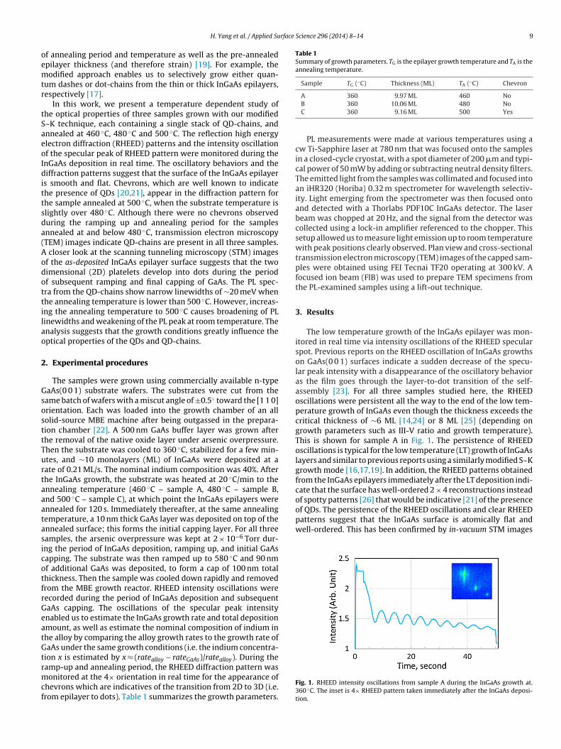
rface Science 296 (2014) 8–14 9
oemtr
tSaeoIdittsda(Aodottilao
2
GsosttTurtaaatasicotfrGeatGtrmcf
Table 1Summary of growth parameters. TG is the epilayer growth temperature and TA is theannealing temperature.
Sample TG (◦C) Thickness (ML) TA (◦C) Chevron
A 360 9.97 ML 460 No
of QDs. The persistence of the RHEED oscillations and clear RHEEDpatterns suggest that the InGaAs surface is atomically flat andwell-ordered. This has been confirmed by in-vacuum STM images
H. Yang et al. / Applied Su
f annealing period and temperature as well as the pre-annealedpilayer thickness (and therefore strain) [19]. For example, theodified approach enables us to selectively grow either quan-
um dashes or dot-chains from the thin or thick InGaAs epilayers,espectively [17].
In this work, we present a temperature dependent study ofhe optical properties of three samples grown with our modified–K technique, each containing a single stack of QD-chains, andnnealed at 460 ◦C, 480 ◦C and 500 ◦C. The reflection high energylectron diffraction (RHEED) patterns and the intensity oscillationf the specular peak of RHEED pattern were monitored during thenGaAs deposition in real time. The oscillatory behaviors and theiffraction patterns suggest that the surface of the InGaAs epilayer
s smooth and flat. Chevrons, which are well known to indicatehe presence of QDs [20,21], appear in the diffraction pattern forhe sample annealed at 500 ◦C, when the substrate temperature islightly over 480 ◦C. Although there were no chevrons observeduring the ramping up and annealing period for the samplesnnealed at and below 480 ◦C, transmission electron microscopyTEM) images indicate QD-chains are present in all three samples.
closer look at the scanning tunneling microscopy (STM) imagesf the as-deposited InGaAs epilayer surface suggests that the twoimensional (2D) platelets develop into dots during the periodf subsequent ramping and final capping of GaAs. The PL spec-ra from the QD-chains show narrow linewidths of ∼20 meV whenhe annealing temperature is lower than 500 ◦C. However, increas-ng the annealing temperature to 500 ◦C causes broadening of PLinewidths and weakening of the PL peak at room temperature. Thenalysis suggests that the growth conditions greatly influence theptical properties of the QDs and QD-chains.
. Experimental procedures
The samples were grown using commercially available n-typeaAs(0 0 1) substrate wafers. The substrates were cut from theame batch of wafers with a miscut angle of ±0.5◦ toward the [1 1 0]rientation. Each was loaded into the growth chamber of an allolid-source MBE machine after being outgassed in the prepara-ion chamber [22]. A 500 nm GaAs buffer layer was grown afterhe removal of the native oxide layer under arsenic overpressure.hen the substrate was cooled to 360 ◦C, stabilized for a few min-tes, and ∼10 monolayers (ML) of InGaAs were deposited at aate of 0.21 ML/s. The nominal indium composition was 40%. Afterhe InGaAs growth, the substrate was heated at 20 ◦C/min to thennealing temperature (460 ◦C – sample A, 480 ◦C – sample B,nd 500 ◦C – sample C), at which point the InGaAs epilayers werennealed for 120 s. Immediately thereafter, at the same annealingemperature, a 10 nm thick GaAs layer was deposited on top of thennealed surface; this forms the initial capping layer. For all threeamples, the arsenic overpressure was kept at 2 × 10⁻⁶ Torr dur-ng the period of InGaAs deposition, ramping up, and initial GaAsapping. The substrate was then ramped up to 580 ◦C and 90 nmf additional GaAs was deposited, to form a cap of 100 nm totalhickness. Then the sample was cooled down rapidly and removedrom the MBE growth reactor. RHEED intensity oscillations wereecorded during the period of InGaAs deposition and subsequentaAs capping. The oscillations of the specular peak intensitynabled us to estimate the InGaAs growth rate and total depositionmount, as well as estimate the nominal composition of indium inhe alloy by comparing the alloy growth rates to the growth rate ofaAs under the same growth conditions (i.e. the indium concentra-
ion x is estimated by x ≈ (ratealloy − rateGaAs)/ratealloy). During the
amp-up and annealing period, the RHEED diffraction pattern wasonitored at the 4× orientation in real time for the appearance ofhevrons which are indicatives of the transition from 2D to 3D (i.e.rom epilayer to dots). Table 1 summarizes the growth parameters.
B 360 10.06 ML 480 NoC 360 9.16 ML 500 Yes
PL measurements were made at various temperatures using acw Ti-Sapphire laser at 780 nm that was focused onto the samplesin a closed-cycle cryostat, with a spot diameter of 200 �m and typi-cal power of 50 mW by adding or subtracting neutral density filters.The emitted light from the samples was collimated and focused intoan iHR320 (Horiba) 0.32 m spectrometer for wavelength selectiv-ity. Light emerging from the spectrometer was then focused ontoand detected with a Thorlabs PDF10C InGaAs detector. The laserbeam was chopped at 20 Hz, and the signal from the detector wascollected using a lock-in amplifier referenced to the chopper. Thissetup allowed us to measure light emission up to room temperaturewith peak positions clearly observed. Plan view and cross-sectionaltransmission electron microscopy (TEM) images of the capped sam-ples were obtained using FEI Tecnai TF20 operating at 300 kV. Afocused ion beam (FIB) was used to prepare TEM specimens fromthe PL-examined samples using a lift-out technique.
3. Results
The low temperature growth of the InGaAs epilayer was mon-itored in real time via intensity oscillations of the RHEED specularspot. Previous reports on the RHEED oscillation of InGaAs growthson GaAs(0 0 1) surfaces indicate a sudden decrease of the specu-lar peak intensity with a disappearance of the oscillatory behavioras the film goes through the layer-to-dot transition of the self-assembly [23]. For all three samples studied here, the RHEEDoscillations were persistent all the way to the end of the low tem-perature growth of InGaAs even though the thickness exceeds thecritical thickness of ∼6 ML [14,24] or 8 ML [25] (depending ongrowth parameters such as III-V ratio and growth temperature).This is shown for sample A in Fig. 1. The persistence of RHEEDoscillations is typical for the low temperature (LT) growth of InGaAslayers and similar to previous reports using a similarly modified S–Kgrowth mode [16,17,19]. In addition, the RHEED patterns obtainedfrom the InGaAs epilayers immediately after the LT deposition indi-cate that the surface has well-ordered 2 × 4 reconstructions insteadof spotty patterns [26] that would be indicative [21] of the presence
Fig. 1. RHEED intensity oscillations from sample A during the InGaAs growth at.360 ◦C. The inset is 4× RHEED pattern taken immediately after the InGaAs deposi-tion.

1 rface
ia
ocooIokt
awwSsBwastrasoasdobinaA
RtdRdtattts
Ffbtj
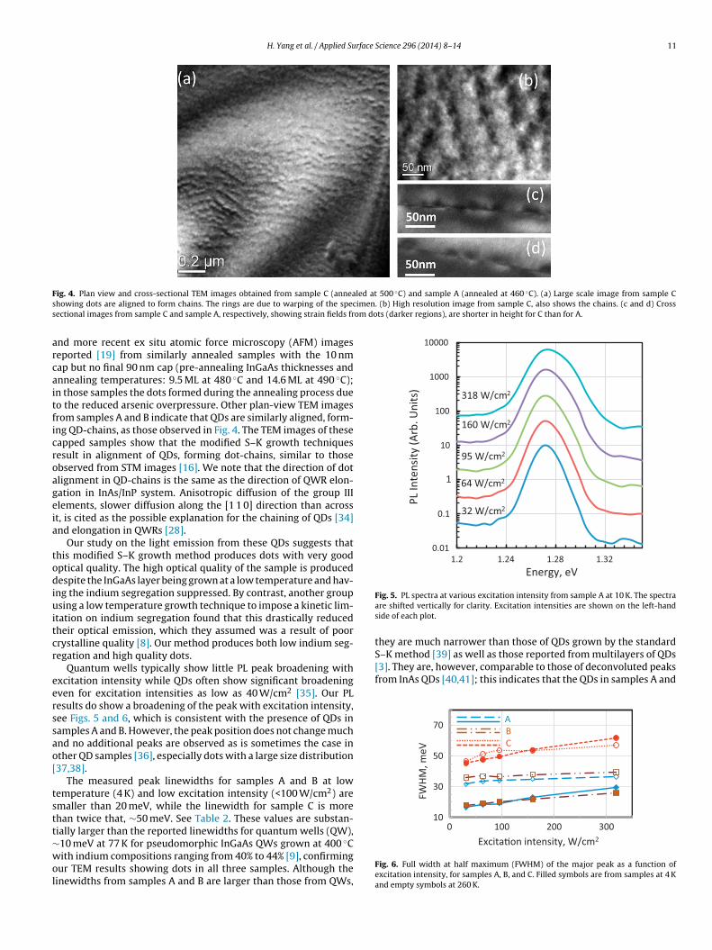
Chaining of QDs is clearly shown in plan-view TEM images. See
0 H. Yang et al. / Applied Su
n our previous report [16] as well as by others [23,26] from thes-grown pre-capped surfaces.
It has been reported that almost no indium segregation isbserved when the substrate temperature is below 370 ◦C [8]. Theonditions that minimize the concentration of group III adatomsn the surface, namely low growth temperature and high arsenicverpressure, have low values for the segregation coefficient [10].n addition to reducing indium segregation, using a high arsenicverpressure during the ramping up and annealing phases helpseep the InGaAs surface smooth and planar, as demonstrated byhe persistent RHEED oscillations.
For sample C, chevrons indicating the formation of QDsppeared at a temperature slightly above 480 ◦C, as the temperatureas increasing to the annealing temperature of 500 ◦C. No chevronsere seen from samples A and B, annealed at lower temperatures.
ince the appearance of chevrons is attributed to the onset of theelf-assembly of QDs [27], the lack of chevrons in samples A and
suggests that the annealed InGaAs surface has a smooth surfaceith platelets [16,23,26], has a very small QD density [19], or has
morphology similar to InAs quantum wires (QWRs) with flat-topurface on InP(0 0 1) in which no chevrons were observed duringhe growth of quantum wires [28]. By contrast, in our previouseport on QD-chains, chevrons appeared at a much lower temper-ture than has been observed here [16]. Part of the reason for theuppression of chevrons in these samples compared to the previ-us ones is the higher arsenic overpressure during the ramping upnd subsequent annealing period; the S–K transition is known to beuppressed under high arsenic overpressure [18] due to the shortiffusion length [29] of group III elements. The effect of arsenicverpressure on diffusion of group III elements is further supportedy the reported observation of the transformation of InAs QWRs
nto QDs on InP(0 0 1) when QWRs are annealed for 120 s undero arsenic overpressure [28]. Despite the lack of chevrons duringnnealing, there is still clear evidence of QD formation in samples
and B; this is described more below.During the initial capping of GaAs, it was possible to obtain
HEED intensity oscillations from sample A and B, persisting tohe end of the GaAs growth, as the RHEED spot of the specular peakid not change after annealing: see Fig. 2. As are confirmed by theHEED and STM studies [23], the observation of RHEED oscillationsuring the whole period of the initial GaAs capping suggests thathe epitaxial growth front remains flat during the periods of thennealing and subsequent GaAs capping. The RHEED patterns afterhe initial GaAs capping, shown in insets in Fig. 2, are less streaky
han those from the pre-annealed InGaAs surface, which suggestshe surface has well-ordered 2 × 4 reconstructions. For these twoamples A and B, the second capping of 90 nm thick GaAs also showig. 2. RHEED intensity oscillations during the initial capping of GaAs immediatelyollowing the annealing. The solid blue line is from sample A at 460 ◦C and dottedrown from sample B at 480 ◦C. The insets are RHEED patterns from sample A, (a)aken immediately after the initial 10 nm GaAs capping at 460 ◦C and (b) at 580 ◦Cust before the deposition of the final 90 nm thick GaAs.
Science 296 (2014) 8–14
good RHEED patterns as well as strong intensity oscillations. Theoscillations of the specular peak were not recorded from sample C,annealed at 500 ◦C, because the specular peak position moved afterthe appearance of chevrons.
Surprisingly, even though the RHEED oscillations continue tobe visible to the end of the initial GaAs capping layer for samplesA and B – which argues against the presence of QDs–TEM imagesof these samples do clearly show QDs. See Fig. 3 as an examplefor sample A, where the wetting layer running along the [1 1 0]direction (the dark line below the dots) is also shown. The seem-ingly contradictory observations of QDs by TEM and well-definedRHEED oscillations during the initial GaAs capping indicate thatthe QDs in samples A and B are induced during the period of ramp-ing up and capping of the top 90 nm of GaAs, instead of during theannealing period. A possible explanation is that platelets act as pre-cursors to QD-chains as they develop into full grown dots due tothe intermixing between Ga and In during ramping up and growthof 90 nm capping at a relatively high temperature of 580 ◦C. Thetemperature of final capping is lower than the typical temperaturein rapid thermal annealing (RTA) [30] but high enough to inducesignificant intermixing [31]. These platelets do not contribute toproduce chevrons as their height is relatively short, about two tothree monolayers, ∼1 nm high, so that the surface is still flat enoughto produce the RHEED oscillations seen both in our study here andby others [23]. A closer look at STM images of the strained-but-flatInGaAs layer confirms the presence of these high density (about 10platelets in 100 × 100 nm2 image, ∼1011/cm2) platelets that haveheights of two to three monolayers and widths of about 10–20 nmwide, see the inset image in Fig. 1 of our previous report [16] as wellas Fig. 1(b) from the report [23] on flat InGaAs layers by anothergroup. The intermixing may dilute the indium concentration in the‘precursor’ platelets but makes them large due to an influx of gal-lium as well as an outflow of indium that expands the boundarywhile the underlying wetting layer connects them to form dot-chains. The transformation of platelets into dots in this study isdifferent in growth mechanism from those reported of 2D precur-sory platelets [32,33] into dots as in the typical S–K growth mode.The preliminary analysis of plan-view TEM images indicates thatthe dot densities are in the order of 1011/cm2. This density is rel-atively high compared to the typical Stranski–Krastanov QDs butconsistent with the platelet density.
As expected from the appearance of chevrons from RHEED mon-itoring, QDs also clearly exist in the TEM images of sample C.
Fig. 4. Chaining of QDs is also apparent in in situ STM images [16]from similarly annealed samples but no capping (pre-annealingInGaAs thicknesses of 10.2 ML at 460 ◦C and 9.6 ML at 480 ◦C)
Fig. 3. Cross-sectional, dark field (220) two-beam condition TEM image of sampleA, annealed at 460 ◦C. The quantum dots are clearly seen in this image.
H. Yang et al. / Applied Surface Science 296 (2014) 8–14 11
F led at 500 ◦C) and sample A (annealed at 460 ◦C). (a) Large scale image from sample Cs imen. (b) High resolution image from sample C, also shows the chains. (c and d) Crosss om dots (darker regions), are shorter in height for C than for A.
arcaitficroageia
todiuitcr
eerssao[
tstt∼wol
0.01
0.1
1
10
100
1000
10000
1.2 1.24 1.28 1.32
32 W/cm2
64 W/cm2
95 W/cm2
318 W/cm2
160 W/cm2
Energy, eV
PL In
tens
ity (A
rb. U
nits
)
S–K method [39] as well as those reported from multilayers of QDs[3]. They are, however, comparable to those of deconvoluted peaksfrom InAs QDs [40,41]; this indicates that the QDs in samples A and
10
30
50
70
0 100 200 300
FWHM
, meV
ABC
ig. 4. Plan view and cross-sectional TEM images obtained from sample C (anneahowing dots are aligned to form chains. The rings are due to warping of the specectional images from sample C and sample A, respectively, showing strain fields fr
nd more recent ex situ atomic force microscopy (AFM) imageseported [19] from similarly annealed samples with the 10 nmap but no final 90 nm cap (pre-annealing InGaAs thicknesses andnnealing temperatures: 9.5 ML at 480 ◦C and 14.6 ML at 490 ◦C);n those samples the dots formed during the annealing process dueo the reduced arsenic overpressure. Other plan-view TEM imagesrom samples A and B indicate that QDs are similarly aligned, form-ng QD-chains, as those observed in Fig. 4. The TEM images of theseapped samples show that the modified S–K growth techniquesesult in alignment of QDs, forming dot-chains, similar to thosebserved from STM images [16]. We note that the direction of dotlignment in QD-chains is the same as the direction of QWR elon-ation in InAs/InP system. Anisotropic diffusion of the group IIIlements, slower diffusion along the [1 1 0] direction than acrosst, is cited as the possible explanation for the chaining of QDs [34]nd elongation in QWRs [28].
Our study on the light emission from these QDs suggests thathis modified S–K growth method produces dots with very goodptical quality. The high optical quality of the sample is producedespite the InGaAs layer being grown at a low temperature and hav-
ng the indium segregation suppressed. By contrast, another groupsing a low temperature growth technique to impose a kinetic lim-
tation on indium segregation found that this drastically reducedheir optical emission, which they assumed was a result of poorrystalline quality [8]. Our method produces both low indium seg-egation and high quality dots.
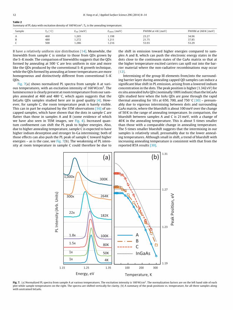
Quantum wells typically show little PL peak broadening withxcitation intensity while QDs often show significant broadeningven for excitation intensities as low as 40 W/cm2 [35]. Our PLesults do show a broadening of the peak with excitation intensity,ee Figs. 5 and 6, which is consistent with the presence of QDs inamples A and B. However, the peak position does not change muchnd no additional peaks are observed as is sometimes the case inther QD samples [36], especially dots with a large size distribution37,38].
The measured peak linewidths for samples A and B at lowemperature (4 K) and low excitation intensity (<100 W/cm2) aremaller than 20 meV, while the linewidth for sample C is morehan twice that, ∼50 meV. See Table 2. These values are substan-ially larger than the reported linewidths for quantum wells (QW),
10 meV at 77 K for pseudomorphic InGaAs QWs grown at 400 ◦Cith indium compositions ranging from 40% to 44% [9], confirmingur TEM results showing dots in all three samples. Although theinewidths from samples A and B are larger than those from QWs,
Fig. 5. PL spectra at various excitation intensity from sample A at 10 K. The spectraare shifted vertically for clarity. Excitation intensities are shown on the left-handside of each plot.
they are much narrower than those of QDs grown by the standard
Excita�on int ensity, W/cm2
Fig. 6. Full width at half maximum (FWHM) of the major peak as a function ofexcitation intensity, for samples A, B, and C. Filled symbols are from samples at 4 Kand empty symbols at 260 K.
12 H. Yang et al. / Applied Surface Science 296 (2014) 8–14
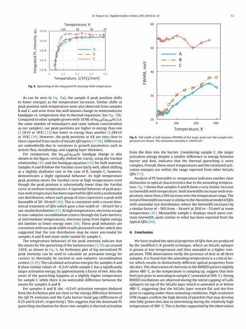
Table 2Summary of PL data with excitation density of 160 W/cm2; TA is the annealing temperature.
Sample TA (◦C) E4 K (meV) E300 K (meV) FWHM at 4 K (meV) FWHM at 260 K (meV)
98
11
16
BltflwhQ
olpIeTcflwtdhtes
Fpw
A 460 1.265 1.1B 480 1.272 1.2C 500 1.286 1.2
have a relatively uniform size distribution [14]. Meanwhile, theinewidth from sample C is similar to those from QDs grown byhe S–K mode. The comparison of linewidths suggests that the QDsormed by annealing at 500 ◦C are less uniform in size and moreike the QDs produced by the conventional S–K growth technique,
hile the QDs formed by annealing at lower temperatures are moreomogeneous and distinctively different from conventional S–KDs.
Fig. 7(a) shows normalized PL spectra from sample A at vari-us temperatures, with an excitation intensity of 160 W/cm2. Theuminescence is clearly present at room temperature from our sam-les annealed at 460 and 480 ◦C, which again suggests that the
nGaAs QDs samples studied here are in good quality [4]. How-ver, for sample C, the room temperature peak is barely visible.his can in part be explained by the STM observations [16] of un-apped samples, which have shown that the dots in sample C areatter than those in samples A and B (some evidence of whiche have also seen in TEM images, see Fig. 4). Increased quan-
um confinement can shift the PL peak to higher energies. Also,ue to higher annealing temperature, sample C is expected to have
igher indium desorption and stronger In-Ga intermixing; both ofhose effects can also push the PL peak of sample C toward highernergies – as is the case, see Fig. 7(b). The weakening of PL inten-ity at room temperature in sample C could therefore be due toPL In
tens
ity (A
rb. U
nits
)
Energy, eV1.15 1.25 1.35
1x
1x
1.5x
1.8x
22x
300x
1,000x
264K
4K
80K
100K
182K
50K
300K
(a)
ig. 7. (a) Normalized PL spectra from sample A at various temperatures. The excitation
lot while sample temperatures on the right. The spectra are shifted vertically for clarityith unstrained InGaAs.
23.27 34.9621.75 37.8553.93 53.29
the shift in emission toward higher energies compared to sam-ples A and B, which can push the electronic energy states in thedots close to the continuum states of the GaAs matrix so that atthe higher temperature excited carriers can spill out into the bar-rier material where the non-radiative recombinations may occur[12].
Intermixing of the group III elements from/into the surround-ing barrier layer during annealing capped QD samples can induce asignificant blue shift in PL emission, arising from a lowered indiumconcentration in the dots. The peak position is higher (1.342 eV) forex situ annealed InAs QDs (nominally 100% indium) than the InGaAsQDs studied here when the InAs QDs are gone through the rapidthermal annealing for 10 s at 650, 700, and 750 ◦C [30] – presum-ably due to vigorous intermixing between dots and surroundingGaAs matrix, where the blueshift is about 100 meV over the changeof 50 K in the range of annealing temperature. In comparison, theblueshift between samples A and C is 21 meV, with a change of40 K in the annealing temperature. This is about 5 times smallerthan those with a comparable change in annealing temperature.The 5 times smaller blueshift suggests that the intermixing in our
samples is relatively small, presumably due to the lower anneal-ing temperatures. Although small in shift, a trend of blueshift withincreasing annealing temperature is consistent with that from thereported RTA results [30].100 200 300
Temperature, K
Peak
Pos
i�on
, eV
1.23
1.19
1.27
1.31
ABCInGaAs
(b)
intensity is 160 W/cm2. The normalization factors are on the left hand side of each. (b) A summary of the peak positions vs. temperature, for all three samples along
H. Yang et al. / Applied Surface Science 296 (2014) 8–14 13
1.E+0
1.E+1
1.E+2
1.E+3
1.E+4
0 0.1 0.2 0.3 0.4
ABC
116 58 39Temperature, K
Temperature, 1/kT(1/meV)
Inte
grat
ed P
L in
tens
ity, a
u. 29
tpBbCta(ataa
srSadptctslrutadcss
t1pccBlofo
ft0q
20
30
40
50
60
0 100 200 300
FWHM
, meV
Temperature, K
ABC
Fig. 8. Quenching of the integrated PL intensity with temperature.
As can be seen in Fig. 7(a), the sample A peak position shiftso lower energies as the temperature increases. Similar shifts ineak position with temperature were also observed from samples
and C, and arise from the well-known change in semiconductorandgaps vs. temperature due to thermal expansion. See Fig. 7(b).ompared to other samples grown with 10 ML of In0.40Ga0.60As (i.e.he same number of monolayers and same indium concentrations our samples), our peak positions are higher in energy than one1.18 eV at 18 K) [14] but lower in energy than another (1.284 eVt 10 K) [39]. However, the peak positions at 4 K are very close tohose reported from stacks of InGaAs QD layers [37,38]. Differencesre undoubtedly due to variations in growth parameters such asrsenic flux, morphology, and capping layer thickness.
For comparison, the In0.40Ga0.60As bandgap change is alsohown in the figure, vertically shifted for clarity, using the Varshnielationship [42] and the bandgap equation [43] for bulk material.amples A and B follow the Varshni curve fairly well, albeit shiftingt a slightly shallower rate in the case of B. Sample C, however,emonstrates a slight sigmoidal behavior: its high temperatureeak position meets the Varshni curve at high temperatures evenhough the peak position is substantially lower than the Varshniurve at medium temperatures. A sigmoidal behavior of peak posi-ion with temperature has been reported for QDs with a multimodalize distribution, where each group of sizes represents a peak withinewidth of 20–30 meV [40]. This is consistent with a recent theo-etical treatment of QDs which gave a line width of ∼20 meV for ani-modal distribution [41]. At high temperatures, electrons escapeo non-radiative recombination centers through the GaAs barriers;t intermediate temperatures, electrons jump from higher energyot families to lower energy ones [40]. These peak behaviors areonsistent with our peak width results presented earlier which alsouggested that the size distribution may be more uni-modal foramples A and B and more multi-modal for sample C.
The temperature behaviors of the peak intensity indicate thathe onsets for the quenching of the luminescence [5,30] are around20 K, as shown in Fig. 8. An Arrhenius plot of log normalized PLeak intensity can be used to calculate an activation energy forarriers to thermally be excited to non-radiative recombinationenters [5,30]. The calculated activation energies for samples A and
show similar values of ∼0.2 eV while sample C has a significantlyarger activation energy, by approximately a factor of two. Also thenset of the quenching happens at a slightly higher temperatureor sample C while there is no noticeable difference between thensets for samples A and B.
For samples A and B, the ∼0.2 eV activation energies deduced
rom the Arrhenius plot are close to the energy difference betweenhe QD PL emission and the GaAs barrier band gap (differences of.25 and 0.24 eV, respectively). This suggests that the dominant PLuenching mechanism for those two samples is thermal activationFig. 9. Full width at half maxima (FWHM) of the major peak over the sample tem-perature are shown. The excitation intensity is 160 W/cm2.
from the dots into the barrier. Considering sample C, the largeractivation energy despite a smaller difference in energy betweenbarrier and dots, indicates that the thermal quenching is morecomplex. Overall, these onset temperatures and the estimated acti-vation energies are within the range reported from other InGaAsQDs [13].
Analysis of PL linewidth vs. temperature indicates another cleardistinction in optical characteristics due to the annealing tempera-ture. Fig. 9 shows that samples A and B show a very similar increasein linewidth with temperature: both linewidths increase with tem-perature, more than a 50% increase over the temperature range. Thetrend of linewidth increase is similar to the theoretical model of QDswith unimodal size distribution, where the linewidth increases bya similar factor of ∼50% from ∼34 meV at 20 K to ∼53 meV at roomtemperature [41]. Meanwhile sample C displays much more con-stant linewidth, quite similar to what has been reported from thetypical QDs [44].
4. Conclusion
We have studied the optical properties of QDs that are producedby the modified S–K growth technique, where an InGaAs epilayeris grown at low temperature and then annealed at a higher tem-perature. TEM observations verify the presence of dots in all threesamples. It is found that the annealing temperature is a critical fac-tor which results in distinctively different optical properties fromthe dots. The observation of chevrons in the RHEED pattern slightlyabove 480 ◦C, as the temperature is ramping up, suggest that dotsform just prior to annealing in sample C (annealed at 500 ◦C). StrongRHEED oscillations are observed during the initial capping of GaAsepilayers on top of the InGaAs layer which is annealed at or below480 ◦C, suggesting that the InGaAs layer remain flat and dot-free
prior to capping under those annealing conditions. High resolutionSTM images confirm the high density of platelets that may developinto fully grown dots due to intermixing during the relatively hightemperature of 580 ◦C. This is further supported by the observation
1 rface
oapttdtcoocwlhpbfed
A
newh
R
[
[
[
[
[
[
[
[
[
[
[
[
[
[
[
[
[
[
[
[
[
[
[
[
[
[
[
[
[
[
[
[
[
[
4 H. Yang et al. / Applied Su
f the similar but unusually high densities dots from TEM imagesnd platelets from STM images. The dots appear to form in sam-les A and B (annealed at 460 ◦C and 480 ◦C, respectively) duringhe subsequent period of GaAs capping, at a much higher tempera-ure of 580 ◦C. The optical properties clearly reflect fundamentallyifferent types of dots being formed when the annealing tempera-ure reaches the critical value of 500 ◦C, with the PL from sample Consistently being different from samples A and B – but similar tother dots prepared with the conventional S–K method – in termsf intensity at room temperature, low temperature linewidths,hange in linewidth with temperature, change in peak positionith temperature, and thermal activation energy. Furthermore, the
inewidth and peak position behaviors suggest that the QDs mayave different size distribution depending on the annealing tem-erature: uni-modal with 480 ◦C or lower annealing temperatureut multi-modal with an annealing temperature of 500 ◦C. There-ore, both the structural as well as the optoelectronic properties ofpitaxial QDs can be fine-tuned by controlling the growth proce-ures.
cknowledgements
Financial support from the National Science Foundation, grantumbers 0854313, 0903804 and 1143543 is gratefully acknowl-dged. We note with sadness the passing of coauthor Steve Brown,ho participated in the experimental phase of the work presentedere.
eferences
[1] W.-H. Chang, T.-M. Hsu, K.-F. Tsai, T.-E. Nee, J.-I. Chyi, N.-T. Yeh, Excitation den-sity and temperature dependent photoluminescence of InGaAs self-assembledquantum dots, Japanese Journal of Applied Physics 38 (1999) 554.
[2] K. Mukai, N. Ohtsuka, M. Sugawara, High photoluminescence efficiency ofInGaAs/GaAs quantum dots self-formed by atomic layer epitaxy technique,Applied Physics Letters 70 (1997) 2416.
[3] K. Kamath, N. Chervela, K.K. Linder, T. Sosnowski, H.T. Jiang, T. Norris, J. Singh,P. Bhattacharya, Photoluminescence and time-resolved photoluminescencecharacteristics of InxGa(1−x)As/GaAs self-organized single- and multiple-layerquantum dot laser structures, Applied Physics Letters 71 (1997) 927.
[4] A. Polimeni, A. Patanè, M. Henini, L. Eaves, P.C. Main, Temperature dependenceof the optical properties of InAs/AlyGa1−yAs self-organized quantum dots, Phys-ical Review B 59 (1999) 5064.
[5] R. Leon, Y. Kim, C. Jagadish, M. Gal, J. Zou, D.J.H. Cockayne, Effects of inter-diffusion on the luminescence of InGaAs/GaAs quantum dots, Applied PhysicsLetters 69 (1996) 1888.
[6] V. Türck, F. Heinrichsdorff, M. Veit, R. Heitz, M. Grundmann, A. Krost, D. Bim-berg, Correlation of InGaAs/GaAs quantum dot and wetting layer formation,Applied Surface Science 123–124 (352) (1998).
[7] A. Patane, A. Polimeni, P.C. Main, M. Henini, L. Eaves, High-temperature lightemission from InAs quantum dots, Applied Physics Letters 75 (1999) 814.
[8] K. Muraki, S. Fukatsu, Y. Shiraki, R. Ito, Surface segregation of In atoms duringmolecular beam epitaxy and its influence on the energy levels in InGaAs/GaAsquantum wells, Applied Physics Letters 61 (1992) 557.
[9] M. Kudo, T. Mishima, Improved photoluminescence properties of highlystrained InGaAs/GaAs quantum wells grown by molecular-beam epitaxy, Jour-nal of Applied Physics 78 (1995) 1685.
10] J.G. Cederberg, Self-assembled quantum dot formation during the growth ofIn0.4Ga0.6As on GaAs(0 0 1) by metal-organic vapor phase epitaxy: the role ofIn segregation, Journal of Crystal Growth 307 (2007) 44.
11] T. Nuytten, M. Hayne, M. Henini, V.V. Moshchalkov, Temperature dependenceof the photoluminescence of self-assembled InAs/GaAs quantum dots in pulsedmagnetic fields, Physical Review B 77 (2008) 115348.
12] S. Sanguinetti, D. Colombo, M. Guzzi, E. Grilli, M. Gurioli, L. Seravalli, P. Frigeri,S. Franchi, Carrier thermodynamics in InAs/InxGa1−xAs quantum dots, PhysicalReview B 74 (2006) 205302.
13] S. Fafard, S. Raymond, G. Wang, R. Leon, D. Leonard, S. Charbonneau, J.L. Merz,P.M. Petroff, J.E. Bowers, Temperature effects on the radiative recombinationin self-assembled quantum dots, Surface Science 361–362 (778) (1996).
14] K. Kamath, P. Bhattacharya, T. Sosnowski, T. Norris, J. Phillips, Room-temperature operation of In0.4Ga0.6As/GaAs self-organised quantum dot lasers,Electronics Letters 32 (1996) 1374.
15] R. Mirin, A. Gossard, J. Bowers, Room temperature lasing from InGaAs quantumdots, Electronics Letters 32 (1996) 1732.
16] D.J. Kim, E.A. Everett, H. Yang, Annealing induced transition of flat strainedInGaAs epilayers into three-dimensional islands, Journal of Applied Physics 101(2007) 106106.
[
Science 296 (2014) 8–14
17] D.J. Kim, H. Yang, Shape control of InGaAs nanostructures on nominalGaAs(0 0 1): dashes and dots, Nanotechnology 19 (2008) 475601.
18] A. Ohtake, M. Ozeki, In situ observation of surface processes in InAs/GaAs(0 0 1)heteroepitaxy: the role of As on the growth mode, Applied Physics Letters 78(2001) 431.
19] K.N. Chauhan, D.M. Riffe, E.A. Everett, D.J. Kim, H. Yang, F.K. Shen, Carrier capturedynamics of single InGaAs/GaAs quantum-dot layers, Journal of Applied Physics113 (2013) 203710.
20] R.P. Mirin, J.P. Ibbetson, K. Nishi, A.C. Gossard, J.E. Bowers, 1.3 �m photolumi-nescence from InGaAs quantum dots on GaAs, Applied Physics Letters 67 (1995)3795.
21] H. Lee, R. Lowe-Webb, W. Yang, P.C. Sercel, Determination of the shape ofself-organized InAs/GaAs quantum dots by reflection high energy electrondiffraction, Applied Physics Letters 72 (1998) 812.
22] D.J. Kim, D. Cha, G.J. Salamo, H. Yang, Enabling in situ atomic scale surface imag-ing for vertical molecular beam epitaxy machines, Journal of Vacuum Science& Technology B: Microelectronics and Nanometer Structures 24 (2006) 2776.
23] C.W. Snyder, B.G. Orr, D. Kessler, L.M. Sander, Effect of strain on surface mor-phology in highly strained InGaAs films, Physical Review Letters 66 (1991)3032.
24] J. Sudijono, M.D. Johnson, C.W. Snyder, M.B. Elowitz, B.G. Orr, Surface evolutionduring molecular-beam epitaxy deposition of GaAs, Physical Review Letters 69(1992) 2811.
25] K. Kamath, P. Bhattacharya, J. Phillips, Room temperature luminescence fromself-organized InxGa1−xAs/GaAs (0.35 < x < 0.45) quantum dots with high sizeuniformity, Journal of Crystal Growth 175–176 (Part 2) (1997) 720.
26] C.W. Snyder, D. Barlett, B.G. Orr, P.K. Bhattacharya, J. Singh, The molecular beamepitaxy growth of InGaAs on GaAs(1 0 0) studied by in situ scanning tunnelingmicroscopy and reflection high-energy electron diffraction, Journal of VacuumScience & Technology B: Microelectronics and Nanometer Structures 9 (1991)2189.
27] Y. Nabetani, T. Ishikawa, S. Noda, A. Sasaki, Initial growth stage and opticalproperties of a three-dimensional InAs structure on GaAs, Journal of AppliedPhysics 76 (1994) 347.
28] H. Yang, P. Ballet, G.J. Salamo, Formation of quantum wires and dots onInP(0 0 1) by As/P exchange, Journal of Applied Physics 89 (2001) 7871.
29] J.Y. Lee, C. Pearson, J.M. Millunchick, Arsenic dependence on the morphologyof ultrathin GaAs layers on In0.53Ga0.47As/InP(0 0 1), Journal of Applied Physics103 (2008) 104309.
30] E.C. Le Ru, J. Fack, R. Murray, Temperature and excitation density dependenceof the photoluminescence from annealed InAs/GaAs quantum dots, PhysicalReview B 67 (2003) 245318.
31] P.B. Joyce, T.J. Krzyzewski, G.R. Bell, B.A. Joyce, T.S. Jones, Composition of InAsquantum dots on GaAs(0 0 1): direct evidence for (In,Ga)As alloying, PhysicalReview B 58 (1998) R15981.
32] C. Priester, M. Lannoo, Origin of self-assembled quantum dots in highly mis-matched heteroepitaxy, Physical Review Letters 75 (1995) 93.
33] Y. Chen, J. Washburn, Structural transition in large-lattice-mismatch heteroepi-taxy, Physical Review Letters 77 (1996) 4046.
34] M. Schmidbauer, Z.M. Wang, Y.I. Mazur, P.M. Lytvyn, G.J. Salamo, D. Grigoriev,P. Schafer, R. Kohler, M. Hanke, Initial stages of chain formation in a single layerof (In,Ga)As quantum dots grown on GaAs (1 0 0), Applied Physics Letters 91(2007) 093110.
35] P. Castrillo, D. Hessman, M.E. Pistol, S. Anand, N. Carlsson, W. Seifert, L. Samuel-son, Band filling at low optical power density in semiconductor dots, AppliedPhysics Letters 67 (1995) 1905.
36] S. Raymond, S. Fafard, P.J. Poole, A. Wojs, P. Hawrylak, S. Charbonneau, D.Leonard, R. Leon, P.M. Petroff, J.L. Merz, State filling and time-resolved pho-toluminescence of excited states in InxGa1−xAs/GaAs self-assembled quantumdots, Physical Review B 54 (1996) 11548.
37] Y.I. Mazur, W.Q. Ma, X. Wang, Z.M. Wang, G.J. Salamo, M. Xiao, T.D. Mishima,M.B. Johnson, InGaAs/GaAs three-dimensionally-ordered array of quantumdots, Applied Physics Letters 83 (2003) 987.
38] T.S. Sosnowski, T.B. Norris, H. Jiang, J. Singh, K. Kamath, P. Bhattacharya, Rapidcarrier relaxation in In0.4Ga0.6As/GaAs quantum dots characterized by differ-ential transmission spectroscopy, Physical Review B 57 (1998) R9423.
39] Y.I. Mazur, B.L. Liang, Z.M. Wang, D. Guzun, G.J. Salamo, G.G. Tarasov, Z.Y.Zhuchenko, Time-resolved photoluminescence spectroscopy of subwettinglayer states in InGaAs/GaAs quantum dot structures, Journal of Applied Physics100 (2006) 054316.
40] L. Brusaferri, S. Sanguinetti, E. Grilli, M. Guzzi, A. Bignazzi, F. Bogani, L. Carraresi,M. Colocci, A. Bosacchi, P. Frigeri, S. Franchi, Thermally activated carrier trans-fer and luminescence line shape in self-organized InAs quantum dots, AppliedPhysics Letters 69 (1996) 3354.
41] B. Bansal, A model for the temperature dependence of photoluminescence fromself-assembled quantum dots, Journal of Applied Physics 100 (2006) 093107.
42] Y.P. Varshni, Temperature dependence of the energy gap in semiconductors,Physica 34 (1967) 149.
43] K.H. Goetz, D. Bimberg, H. Jurgensen, J. Selders, A.V. Solomonov, G.F. Glinskii, M.Razeghi, Optical and crystallographic properties and impurity incorporation ofGaxIn1−xAs (0.44 < x < 0.49) grown by liquid phase epitaxy, vapor phase epitaxy,
and metal organic chemical vapor deposition, Journal of Applied Physics 54(1983) 4543.44] S. Sanguinetti, M. Henini, M. Grassi Alessi, M. Capizzi, P. Frigeri, S. Franchi, Car-rier thermal escape and retrapping in self-assembled quantum dots, PhysicalReview B 60 (1999) 8276.