Applied Materials is accelerating Solar - pole-derbi.com Romain Beau de Lomenie ERBI... · Applied...
17
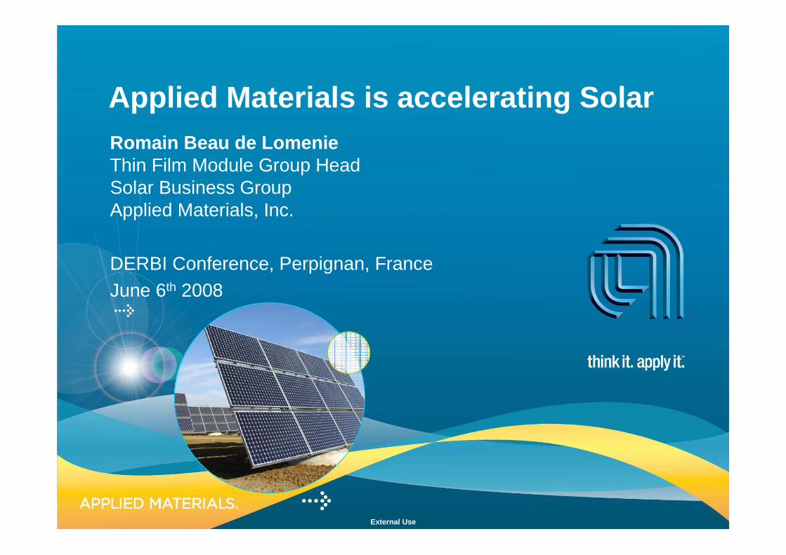
External Use Applied Materials is accelerating Solar Romain Beau de Lomenie Thin Film Module Group Head Solar Business Group Applied Materials, Inc. DERBI Conference, Perpignan, France June 6 th 2008
Transcript of Applied Materials is accelerating Solar - pole-derbi.com Romain Beau de Lomenie ERBI... · Applied...
External Use
Applied Materials is accelerating SolarRomain Beau de LomenieThin Film Module Group HeadSolar Business GroupApplied Materials, Inc.
DERBI Conference, Perpignan, FranceJune 6th 2008
External Use2
Safe Harbor StatementThis presentation contains forward-looking statements, including those relating to Applied Materials’ growth opportunities, product capabilities. acquired businesses, cost-per-watt-reduction strategy, efficiency roadmap, solar contracts, and financial goals. These statements are subject to known and unknown risks and uncertainties that could cause actual results to differ materially from those expressed or implied by such statements, including but not limited to: demand for solar products, which is subject to many factors, including global economic and market conditions, government policies and incentives relating to renewable energy, technological innovations, the cost of competing sources of energy, and evolving industry standards; the performance of acquired businesses; Applied’s ability to (i) successfully develop, deliver and support its broad range of products and expand its markets and develop new markets, (ii) effectively manage its resources and production capability, (iv) accurately predict the characteristics of, and capitalize on opportunities in, emerging markets, and (v) attract and retain key employees; and other risks described in Applied’s SEC filings. All forward-looking statements are based on management’s estimates, projections and assumptions as of February 20, 2008, and Applied undertakes no obligation to update any such statements.
External Use3
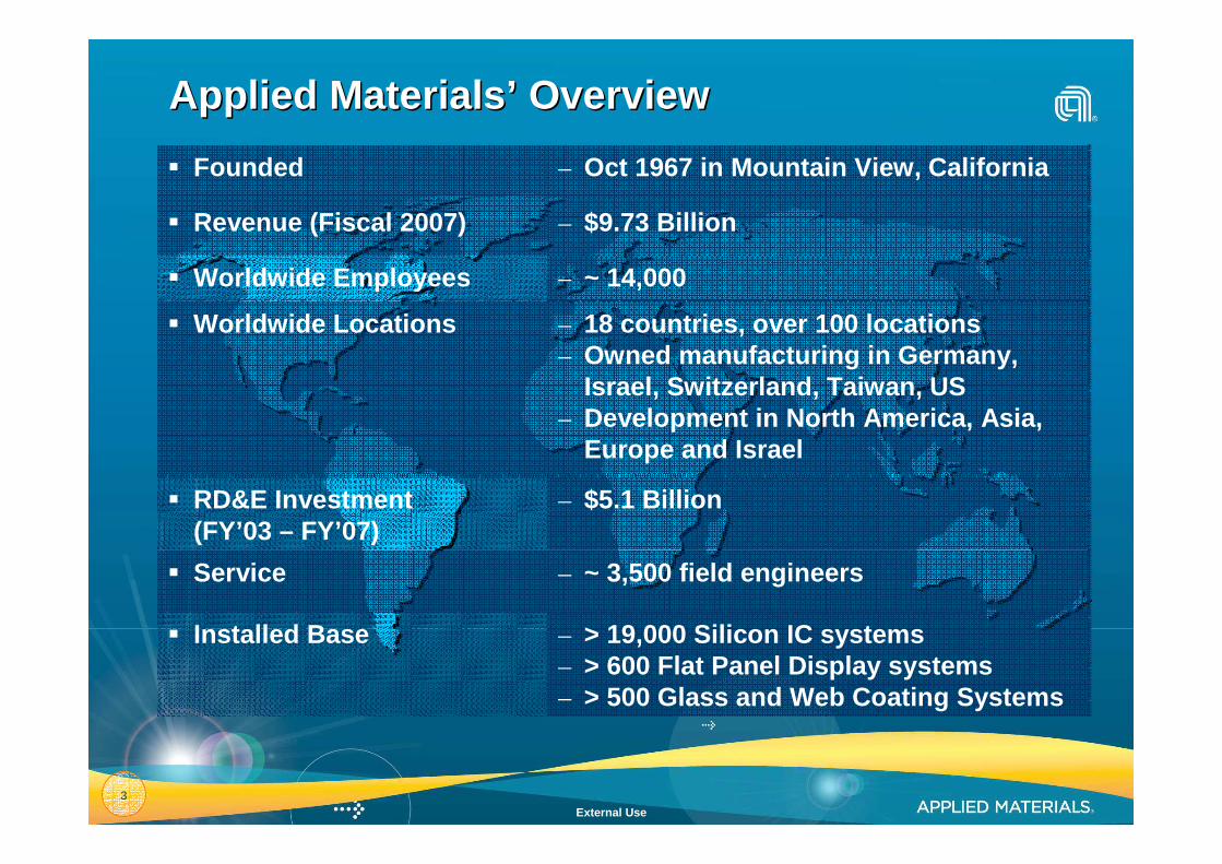
– Oct 1967 in Mountain View, California� Founded
– > 19,000 Silicon IC systems– > 600 Flat Panel Display systems– > 500 Glass and Web Coating Systems
� Installed Base
– ~ 3,500 field engineers� Service
– $5.1 Billion� RD&E Investment (FY’03 – FY’07)
– 18 countries, over 100 locations– Owned manufacturing in Germany,
Israel, Switzerland, Taiwan, US– Development in North America, Asia,
Europe and Israel
� Worldwide Locations
– ~ 14,000� Worldwide Employees
– $9.73 Billion� Revenue (Fiscal 2007)
Applied MaterialsApplied Materials ’’ OverviewOverview
External Use4
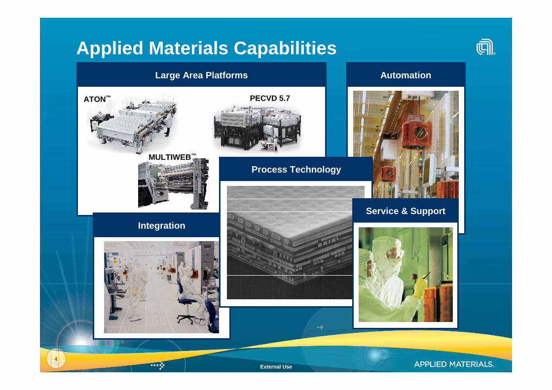
Large Area Platforms
ATON™
MULTIWEB™
PECVD 5.7
Applied Materials Capabilities
Integration
Automation
Process Technology
Service & Support
External Use5
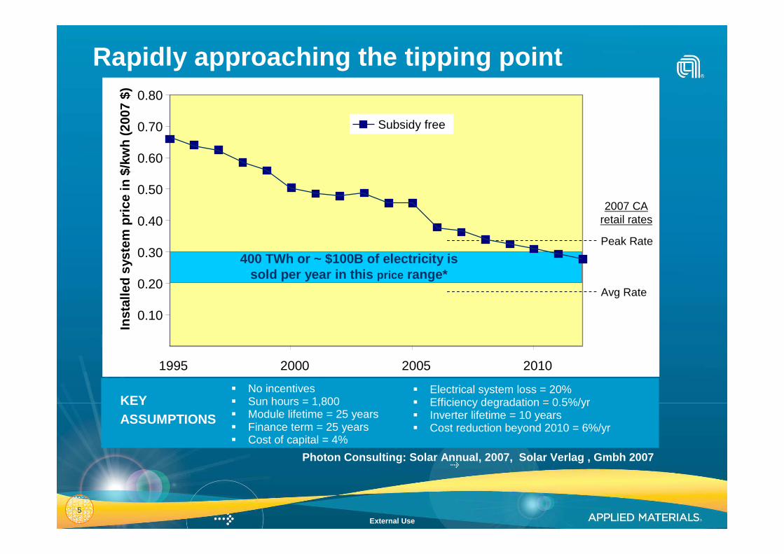
Rapidly approaching the tipping point
Peak Rate
Avg Rate
2007 CAretail rates
400 TWh or ~ $100B of electricity is sold per year in this price range*
0.10
0.20
0.30
0.40
0.50
0.60
0.70
0.80
1995 2000 2005 2010
Inst
alle
d sy
stem
pric
e in
$/k
wh
(200
7 $)
Subsidy free
Photon Consulting: Solar Annual, 2007, Solar Verla g , Gmbh 2007
� No incentives� Sun hours = 1,800� Module lifetime = 25 years� Finance term = 25 years� Cost of capital = 4%
� Electrical system loss = 20%� Efficiency degradation = 0.5%/yr� Inverter lifetime = 10 years� Cost reduction beyond 2010 = 6%/yr
KEYASSUMPTIONS

External Use6
Mid-Size Installations (no ITC)
Utility Scale PV electricity
Peak Rate
Avg Rate
Assumptions:PV Cost reduction past 2010 = 6% per yearUtility rate increase = 3% per year
0.00
0.05
0.10
0.15
0.20
0.25
0.30
0.35
0.40
0.45
0.50
2006 2008 2010 2012 2014 2016 2018 2020
Price below which PV goes mainstream ($2.50 - $3.00 $/Wp)
Inst
alle
d sy
stem
pric
e $/
kWh
(200
7 $)

External Use7
Cost per watt
Extending Cost Reduction Focus to SolarExtending Cost Reduction Focus to Solar
5 nano-dollars10 cents
1,400,000 trillion4 trillion
20041974
20,000,000x Cost Reduction
Source: SIA, IC Knowledge LLC$1,500/m2$30,000/m2
25 million /m20.3 million/m2
20051995
20x Cost ReductionSource: Display Search, Nikkei BP, Applied Materials
Cost per transistor
FIRSTFIRST
Cost per area
THENTHEN
NOWNOW
External Use8
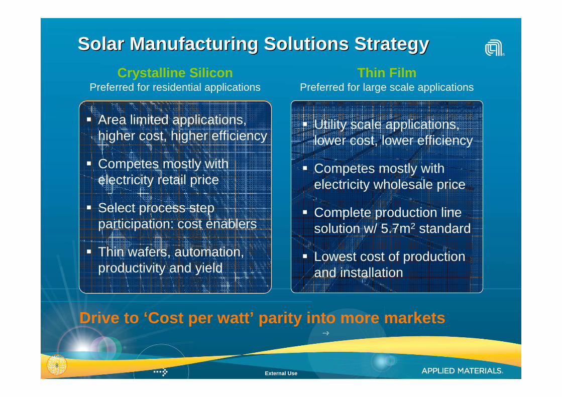
Crystalline SiliconPreferred for residential applications
Thin FilmPreferred for large scale applications
� Area limited applications, higher cost, higher efficiency
� Competes mostly with electricity retail price
� Select process step participation: cost enablers
� Thin wafers, automation, productivity and yield
� Utility scale applications, lower cost, lower efficiency
� Competes mostly with electricity wholesale price
� Complete production line solution w/ 5.7m2 standard
� Lowest cost of production and installation
Solar Manufacturing Solutions StrategySolar Manufacturing Solutions Strategy
Drive to ‘Cost per watt’ parity into more markets

External Use9
c-Si: Focus on High Value Processes
Thin Wafer Processing
� High Productivity Systems
� Cell Efficient Processes
� Low Manufacturing Cost
InstallationModuleLaminateCell Production / ManufactureWaferingIngotsPoly
SiliconStep Names Inspect / Test
Edge IsolationMetallizationPassivationEmitter
FormationSaw
Damage
Applied’s c-Si Defined TAM
Applied’s 2008 c-Si SAM ~42% of c-Si TAM
Pho
to

External Use10
Scaling up: Scaling up: SunFabSunFab ™™ Thin Film LineThin Film Line
� Complete production line of world largest 5.7m2 largest PV modules
� Thin film silicon glass-PVB-glass module design
� 50MW~75MW single line capacity w/ multi-line GW capacity design
� 2010 goals: $1.00/Wp production cost @10% efficiency
� > 20% reduction in BOS cost with large size and bonded rail design
External Use11
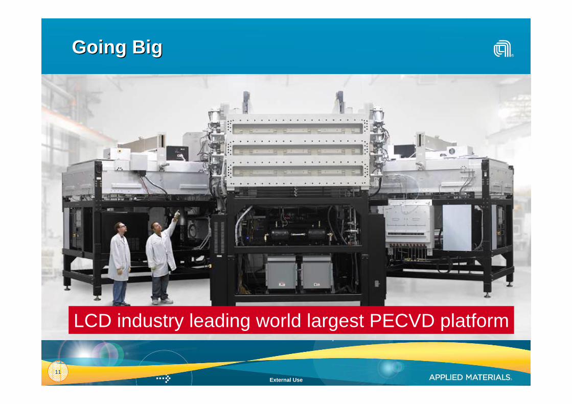
Going BigGoing Big
LCD industry leading world largest PECVD platform
External Use12
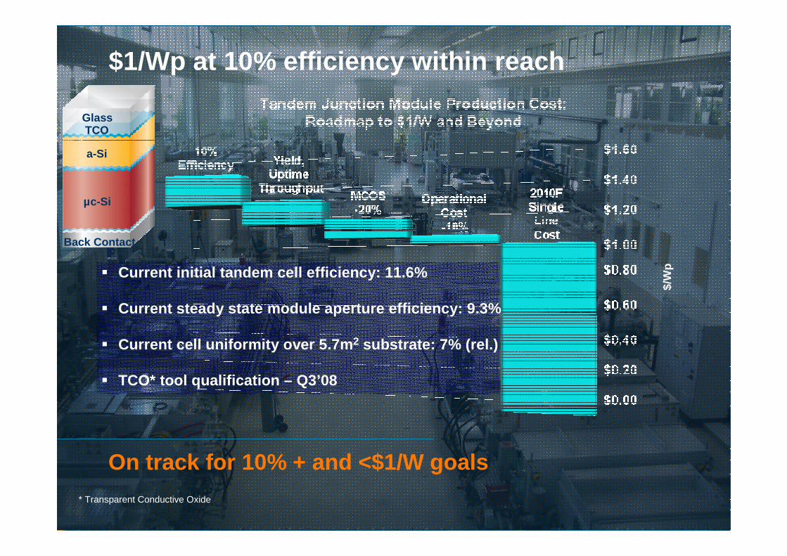
$1/Wp at 10% efficiency within reach
� Current initial tandem cell efficiency: 11.6%
� Current steady state module aperture efficiency: 9. 3%
� Current cell uniformity over 5.7m 2 substrate: 7% (rel.)
� TCO* tool qualification – Q3’08
* Transparent Conductive Oxide
$/W
p
On track for 10% + and <$1/W goals
µc-Si
a-Si
TCOGlass
Back Contact
External Use13
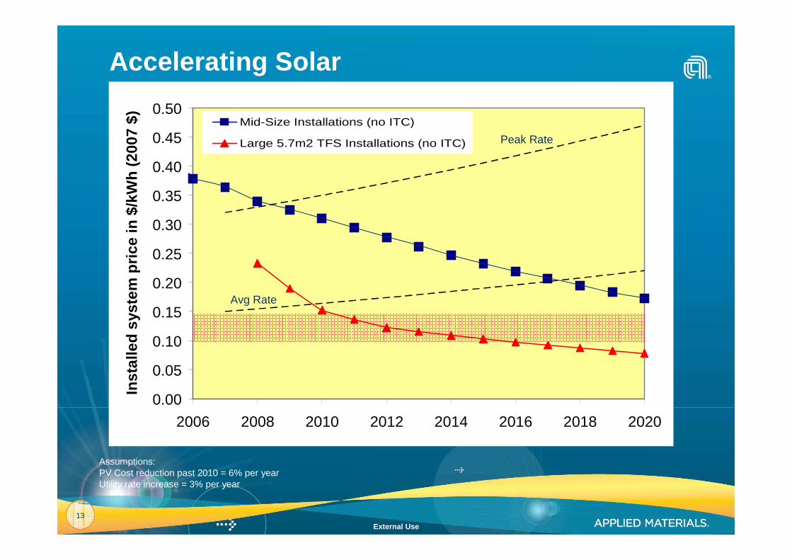
Mid-Size Installations (no ITC)
Large 5.7m2 TFS Installations (no ITC)
Accelerating Solar
Peak Rate
Avg Rate
Assumptions:PV Cost reduction past 2010 = 6% per yearUtility rate increase = 3% per year
0.00
0.05
0.10
0.15
0.20
0.25
0.30
0.35
0.40
0.45
0.50
2006 2008 2010 2012 2014 2016 2018 2020
Inst
alle
d sy
stem
pric
e in
$/k
Wh
(200
7 $)

External Use14
Summary
� Applied Materials is extending its cost reduction focus to Solar
� cSi: residential market, strong portfolio in cost enabling steps, focus on thin wafers and automation
� Thin film: utility scale market, Sunfab enables PV to go mainstream by 2010
� Sunfab sets the 5.7m2 standard, allowing rapid adoption and scaling globally with > 2GW of announced capacity sold
Applied Materials is accelerating Solar!

External Use15

External Use16
Applied Materials Reporting Segments
AdjacentAdjacentTechnologiesTechnologies
Design, manufacture, sale and service of equipment used to fabricate solar cells, flexible electronics and energy-efficient glass
Manufacture and sale of equipment to fabricate semiconductor chipsSiliconSilicon
Broad range of products1 to maintain, service and optimize customers’ semiconductor fabs
FabFabSolutionsSolutions
Design, manufacture, sale, and services of equipment used to make flat panel displaysDisplayDisplay

External Use17
1
10
100
1,000
10,000
100,000
2000 2010F 2020F 2030F 2040F
TW
h1 /
Yea
r
Solar Electricity Production (TWh)
1 TWh = Terrawatt-hour = 1 Billion Kilowatt-hours2 GWp = Gigawatt-peak, assuming average hours or sunshine Source: Solar Generation and IEA-PVPS
Total Electricity Production
10% Total
1% Total
World Electricity Production ForecastWorld Electricity Production Forecast(2000 (2000 –– 2040)2040)
US
= Consumption in labeled country/state
China
India
California 1 Million Roofs
Est. CAGR% ’00 - ’40Total Electricity Production 2.5%
(increase of 25,400TWh)Solar Energy Production 21%
(increase of 6,000TWh) ~5
~50
~500
~5,000
Equivalent Solar GWp 2
Current solar capacity
Potential of Existing US Rooftops (GWp)