ANGLE-RESOLVED PHOTOEMISSION AND FIRST-PRINCIPLES STUDIES...
218
ANGLE-RESOLVED PHOTOEMISSION AND FIRST-PRINCIPLES STUDIES OF TOPOLOGICAL THIN FILMS BY GUANG BIAN DISSERTATION Submitted in partial fulfillment of the requirements for the degree of Doctor of Philosophy in Physics in the Graduate College of the University of Illinois at Urbana-Champaign, 2012 Urbana, Illinois Doctoral Committee: Professor S. Lance Cooper, Chair Professor Tai-Chang Chiang, Director of Research Professor Michael Stone Professor Jen-Chieh Peng
Transcript of ANGLE-RESOLVED PHOTOEMISSION AND FIRST-PRINCIPLES STUDIES...

ANGLE-RESOLVED PHOTOEMISSION AND FIRST-PRINCIPLES STUDIES OF TOPOLOGICAL THIN FILMS
BY
GUANG BIAN
DISSERTATION
Submitted in partial fulfillment of the requirements for the degree of Doctor of Philosophy in Physics
in the Graduate College of the University of Illinois at Urbana-Champaign, 2012
Urbana, Illinois
Doctoral Committee: Professor S. Lance Cooper, Chair Professor Tai-Chang Chiang, Director of Research Professor Michael Stone Professor Jen-Chieh Peng


ii
Abstract
Topological insulators are electronic materials that have a bulk band gap like an
ordinary insulator but have protected conducting states on their edge or surface. The
exotic electronic properties of topological materials are of great interest for spin-related
electronics and quantum computation. In this thesis research, the combination of angle-
resolved photoemission spectroscopy (ARPES) and first principles calculation is used to
examine the electronic properties of topological thin films and 2D electronic systems
with large spin-orbit splitting. The topological thin films are prepared in situ by
molecular beam epitaxy (MBE) method and characterized by experimental tools such as
reflection high-energy electron diffraction (RHEED) and low energy electron diffraction
(LEED). The systems investigated in this thesis include topological Sb, Bi2Te3, Be2Se3
thin films, Bi films, and Bi/Ag surface alloy.
Topological Sb films have been successfully fabricated on Si(111) substrates. By
examining the connection pattern between surface states and the quantum well bulk states,
our photoemission spectra show clearly the topological order of the Sb films. When
topological films become ultrathin, the quantum tunneling effect breaks the degeneracy at
the Dirac point of the topological surface bands, resulting in a gap. Our ARPES mapping
of the surface band structure of a 4-BL Sb film reveals no energy gap at the Dirac point.
This lack of tunneling gap can be explained by a strong interfacial bonding between the
film and the substrate.
The topological order of topological materials is a robust quantity, but the
topological surface states themselves can be highly sensitive to the boundary conditions.
Specifically, the surface states of Bi2Se3 and Bi2Te3 form a single Dirac cone at the zone
center. Our first-principles calculations based on a slab geometry show that, upon
hydrogen termination of either face of the slab, the Dirac cone associated with this face is
replaced by three Dirac cones centered at the time-reversal-invariant M points at the
zone boundary. The critical behavior of the TI film near the quantum critical point is also

iii
studied theoretically. When the strength of the spin-orbit coupling (SOC) is tuned across
the critical point, the topological surface states, while protected by symmetry in the bulk
limit, can be missing completely in topological films even at large film thicknesses.
We have observed, using angle-resolved photoemission, a structural phase
transformation of Bi films deposited on Si(111)-(77). Films with thicknesses 20 to ~100
Å, upon annealing, first order into a metastable pseudocubic (PC) phase and then
transform into a stable rhombohedral (RH) phase with very different topologies for the
quantum well subband structures. The PC phase shows a surface band with a maximum
near the Fermi level at , whereas the RH phase shows a Dirac-like subband around M
along K M K . The formation of the metastable phase over a wide thickness range can
be attributed to a surface nucleation mechanism.
Finally, we have studied the electronic structure of the Bi/Ag surface alloy, a system
possessing a huge Rashba splitting in its surface bands. The Bi/Ag surface alloy is
prepared by depositing Bi onto ultrathin Ag films followed by annealing. The electronic
structure of the system is measured using circular angle resolved photoemission
spectroscopy (CARPES). The results reveal two interesting phenomena: the hybridization
of spin polarized surface states with Ag bulk quantum well states and the umklapp
scattering by the perturbed surface potential. In addition, our CARPES spectra show
clearly a unique dichroism pattern which is closely related to the spin texture of this 2D
strongly spin-orbit coupled electron system.

iv
Acknowledgements
First and foremost, I would like to thank my advisor, Professor Tai-Chang Chiang,
for his guidance, support and encouragement throughout the course of this work. I owe
special thanks to Dr. Thomas J. Miller. The data comprising this thesis could not have
been taken without his assistance and technical expertise.
I’ve enjoyed very much working with present and past group members Dr. Ruqing
Xu, Dr. Yang Liu, Dr. Matthew Brinkley, Dr. Aaron Gray, Dr. Xiaoxiong Wang, Dr.
Huanhua Wang, Dr. Gazzy Weng, Longxiang Zhang, Caizhi Xu, Man-Hong Wong, Jie
Ren and Xinyue Fang. I am also grateful to the staff scientists at the SRC for their
technical support of my experiments. Thanks to Prof. Simon Brown, Dr. Pawel
Kowalczyk and Ojas Mahapatra for the enjoyable collaboration.
I would like to mention my friends Dr. Hefei Hu, Jia Gao, Ching-Kai Chiu, Xianhao
Xin, Han Cheng, Gang Ling and Yaxuan Yao, who made the days at Urbana so pleasant
and memorable.
In particular, I wish to thank my parents for their support and understanding during
all my studies.
The thesis is based on work supported by the U.S. Department of Energy, under
Grant No. DE-FG02-07ER46383. I acknowledge partial financial support by the Yee
Memorial Fund Fellowship. The Synchrotron Radiation Center, where the ARPES data
were taken, is supported by the U.S. National Science Foundation (Grant DMR-05-
37588). Acknowledgement is also made to the ACS Petroleum Research Fund and the
U.S. National Science Foundation (Grant DMR-09-06444) for partial support of beamline
operations.

v
Table of Contents
Page
List of Symbols and Abbreviations . . . . . . . . . . . . . . . . . . . . . . . . viii
1 Introduction . . . . . . . . . . . . . . . . . . . . . . . . . . . . . . . . . . . . 1
1.1 Topological thin films and quantum size effect . . . . . . . . . . . . . . . . 1
1.2 Thesis overview . . . . . . . . . . . . . . . . . . . . . . . . . . . . . . . . 3
References . . . . . . . . . . . . . . . . . . . . . . . . . . . . . . . . . . 3
2 Experimental Techniques . . . . . . . . . . . . . . . . . . . . . . . . . . . . 5
2.1 Introduction . . . . . . . . . . . . . . . . . . . . . . . . . . . . . . . . . 5
2.2 Surface reconstruction . . . . . . . . . . . . . . . . . . . . . . . . . . . . 5
2.3 Molecular beam epitaxy . . . . . . . . . . . . . . . . . . . . . . . . . . . 6
2.4 Reflection high-energy electron diffraction . . . . . . . . . . . . . . . . . 7
2.5 Low energy electron diffraction. . . . . . . . . . . . . . . . . . . . . . . 8
References . . . . . . . . . . . . . . . . . . . . . . . . . . . . . . . . . . 9
Figures . . . . . . . . . . . . . . . . . . . . . . . . . . . . . . . . . . . . 10
3 Angle-Resolved Photoemission Spectroscopy . . . . . . . . . . . . . . . . . 17
3.1 Introduction . . . . . . . . . . . . . . . . . . . . . . . . . . . . . . . . . 17
3.2 An intuitive view of photoemission process . . . . . . . . . . . . . . . . 17
3.3 ARPES experimental apparatus . . . . . . . . . . . . . . . . . . . . . . . 21
3.4 Theory of photoemission spectroscopy. . . . . . . . . . . . . . . . . . . . 23
References . . . . . . . . . . . . . . . . . . . . . . . . . . . . . . . . . . 29
Figures . . . . . . . . . . . . . . . . . . . . . . . . . . . . . . . . . . . . 31
4 Theoretical Background . . . . . . . . . . . . . . . . . . . . . . . . . . . . 39
4.1 Introduction. . . . . . . . . . . . . . . . . . . . . . . . . . . . . . . . . 39
4.2 Surface states. . . . . . . . . . . . . . . . . . . . . . . . . . . . . . . . . 39
4.3 Quantum well states. . . . . . . . . . . . . . . . . . . . . . . . . . . . . . 40
4.4 Rashba effect. . . . . . . . . . . . . . . . . . . . . . . . . . . . . . . . . 43

vi
4.5 Topological insulator and topological order . . . . . . . . . . . . . . . . . 45
4.6 Density functional theory. . . . . . . . . . . . . . . . . . . . . . . . . . 46
References. . . . . . . . . . . . . . . . . . . . . . . . . . . . . . . . . . 49
Figures. . . . . . . . . . . . . . . . . . . . . . . . . . . . . . . . . . . . 51
5 Topological Sb Thin Films . . . . . . . . . . . . . . . . . . . . . . . . . . . 61
5.1 Introduction . . . . . . . . . . . . . . . . . . . . . . . . . . . . . . . . . 61
5.2 Experimental preparation of Sb films . . . . . . . . . . . . . . . . . . . . 62
5.3 Bulk band structure of Sb. . . . . . . . . . . . . . . . . . . . . . . . . . 63
5.4 Passage from spin polarized TSS to spin degenerate QWS. . . . . . . . . 64
5.5 Quantum tunneling effect in ultrathin Sb films . . . . . . . . . . . . . . . 68
5.6 Conclusion . . . . . . . . . . . . . . . . . . . . . . . . . . . . . . . . . . 75
References . . . . . . . . . . . . . . . . . . . . . . . . . . . . . . . . . . 76
Figures . . . . . . . . . . . . . . . . . . . . . . . . . . . . . . . . . . . . 79
6 Topological Thin Films: Bi2Se3 and Bi2Te3 . . . . . . . . . . . . . . . . . . 95
6.1 Introduction . . . . . . . . . . . . . . . . . . . . . . . . . . . . . . . . . 95
6.2 Reorganization of Dirac cones in topological insulators by hydrogen
termination . . . . . . . . . . . . . . . . . . . . . . . . . . . . . . . . . 96
6.3 Evolution of the band structure upon varying the hydrogen atom position . 100
6.4 Hydrogen-induced bonding states below the p valence bands . . . . . . . 101
6.5 Robustness of the first-principles results . . . . . . . . . . . . . . . . . . 102
6.6 Bulk band structures and parity eigenvalues of Bi2Se3 with/without SOC . 102
6.7 Topological phase transition and Dirac fermion transfer in Bi2Se3 films . . 103
6.8 Band structures of a 6-QL Bi2Se3 film with the top face terminated
by F or Cl. . . . . . . . . . . . . . . . . . . . . . . . . . . . . . . . . . . 107
6.9 Conclusion . . . . . . . . . . . . . . . . . . . . . . . . . . . . . . . . . . 108
References . . . . . . . . . . . . . . . . . . . . . . . . . . . . . . . . . 109
Figures and tables. . . . . . .. . . . . . . . . . . . . . . . . . . . . . . . 111
7 Epitaxial Bi Films on Si(111): Surface-Mediated Metastability . . . . . . . 125
7.1 Introduction . . . . . . . . . . . . . . . . . . . . . . . . . . . . . . . . . 125
vii
7.2 Sample preparation and computational methods . . . . . . . . . . . . . . 126
7.3 Metastability of epitaxial Bi films . . . . . . . . . . . . . . . . . . . . . . 127
7.4 Conclusion . . . . . . . . . . . . . . . . . . . . . . . . . . . . . . . . . 131
References . . . . . . . . . . . . . . . . . . . . . . . . . . . . . . . . . . 132
Figures . . . . . . . . . . . . . . . . . . . . . . . . . . . . . . . . . . . 134
8 Giant-Rashba System: Bi/Ag(111) Surface Alloy . . . . . . . . . . . . . . . 139
8.1 Introduction . . . . . . . . . . . . . . . . . . . . . . . . . . . . . . . . . 139
8.2 Preparation of Bi/Ag(111) surface alloy and CAPRES measurement . . . 140
8.3 The surface spin texture of the Bi/Ag(111) surface alloy studied by
circularly-polarized photoemission . . . . . . . . . . . . . . . . . . . . . 140
8.4 Transition matrix elements for surface photoemission. . . . . . . . . . . . 146
8.5 CARPES spectra of Ag quantum well states. . . . . . . . . . . . . . . . . 147
8.6 First-principles study of a single Bi/Ag layer. . . . . . . . . . . . . . . . 147
8.7 Conclusion . . . . . . . . . . . . . . . . . . . . . . . . . . . . . . . . . 152
References . . . . . . . . . . . . . . . . . . . . . . . . . . . . . . . . . 153
Figures . . . . . . . . . . . . . . . . . . . . . . . . . . . . . . . . . . . 156
9 Summary and Outlook . . . . . . . . . . . . . . . . . . . . . . . . . . . . . 169
Appendices . . . . . . . . . . . . . . . . . . . . . . . . . . . . . . . . . . . . 173
Appendix A Computational software: ABINIT . . . . . . . . . . . . . . . . 173
Appendix B Rhombohedral lattices of Bi, Sb, Bi2Te3 and Bi2Se3 . . . . . . . 176
Appendix C Surface states, quantum well states and excited states
of Ag (111) films . . . . . . . . . . . . . . . . . . . . . . . . 178
Appendix D Topological phase transition in the Kane-Mele model. . . . . . 180
Appendix E Probing Berry’s phase in graphene by circular ARPES . . . . . 185
References . . . . . . . . . . . . . . . . . . . . . . . . . . . 188
Figures and tables. . . . . . . . . . . . . . . . . . . . . . . . 190
Author’s Biography . . . . . . . . . . . . . . . . . . . . . . . . . . . . . . . . 205

viii
List of Symbols and Abbreviations
hv Photon energy
BE Electron binding energy (relative to the Fermi level)
FE Fermi Energy
k
Electron wave vector
Å Angstrom (10-10 m or 0.1 nm)
1D, 2D, 3D One-, Two-, Three-Dimensional
ARPES Angle-Resolved Photoemission Spectroscopy
Ag Silver
Au Gold
Bi Bismuth
Sb Antimony
Si Silicon
Se Selenium
Te Tellurium
ML Monolayer
BL Bilayer
SIA Structural Inversion Asymmetry
UHV Ultrahigh Vacuum

ix
MBE Molecular Beam Epitaxy
LEED Low-Energy Electron Diffraction
RHEED Reflection High-Energy Electron Diffraction
SRC Synchrotron Radiation Center
EDC Energy Distribution Curve
MDC Momentum Distribution Curve
DOS Density of States
QWS Quantum Well State
SS Surface State
TSS Topological Surface State
TI Topological Insulator
TRIM Time Reversal Invariant Momentum
BZ Brillouin Zone
SBZ Surface Brillouin Zone
DFT Density Functional Theory
LDA Local Density Approximation
GGA Generalized Gradient Approximation
FCC Face-Centered Cubic
PC Pseudocubic
RH Rhombohedral
RT Room Temperature

x
SA Surface Alloy
TB Tight Binding
HP Horizontally Polarized
VP Vertically Polarized
LCP Left-handed Circularly Polarized
RCP Right-handed Circularly Polarized

1
1 Introduction
1.1 Topological thin films and quantum size effect
Topological materials present opportunities for realizing new fundamental physics,
novel devices for spintronics, and quantum computation [1,2] which may be facilitated
through the realization of exotic states such as Majorana fermions [3] and magnetic
monopoles [4]. Topological thin films grown on semiconductor substrates have great
potential for future device applications. When the thickness of a thin film becomes
comparable to the electronic coherence length, quantum size effects can alter greatly
physical properties [5,6]. A direct consequence of such effects is the formation of
electronic standing waves, i.e., quantum well states (QWS) [7,8]. Quantum size effects
have been well known to exert a thickness-dependent modulation on thermal and
transport properties of nanoscale systems. For example, the superconducting transition
temperature of Pb films oscillates with the increasing film thickness [9]. The thermal
stability of metal thin films also critically depends on the film thickness [10]. Quantum
size effects have even more profound influences on topological thin films due to the
presence of the topological ordering and the protected surface states. Topological
insulator thin films show an oscillatory behavior as a function of the layer thickness,
alternating between topologically trivial and nontrivial order [ 11 ]. Moreover, the
quantum tunneling effect, intrinsic to thin films, opens a thickness-dependent energy gap
at the Dirac point of the topological surface bands, which opens a door for manipulating
the spin current on the surface of topological insulators [12].
Exciting physics can arise from the interplay between quantum size effects and
topological ordering. However, up to now, experimental investigations of nanoscale

2
topological systems have not been well established due to the stringent material
engineering requirements. Considerable effort of my thesis research has been put on
fabrication of atomically uniform topological thin films on semiconductor substrates by
molecular beam epitaxy (MBE) technique. The surface condition of the substrates is
crucially important for the structural quality of the epitaxial thin films. The electronic
structure of the epitaxial grown thin films is examined by a combined method of
angle-resolved photoemission spectroscopy (ARPES) and first-principles calculation. The
spectroscopic information of the thin films can provide a deep understanding of the
transport properties and a significant guidance for practical device applications. The
procedure of the research works reported in this thesis basically consists of three parts:
1. MBE growth of atomically uniform thin films and surface characterization,
2. Synchrotron-based ARPES measurement of the electronic band structure,
3. Theoretical modeling and first-principles calculations.
This dissertation examines the electronic properties of topological Sb, Bi2Te3,
Be2Se3 thin films [13,14,15,16,17]. Besides the topological thin films, Bi films and Bi/Ag
surface alloy are the other two systems studied in this thesis [18,19]. Semi-metallic Bi is
one of the parent ingredients of the alloy topological insulater Bi1-xSbx (0.07 < x < 0.2)
[20,21]. But, unlike Sb, Bi doesn’t share the nontrivial topological order of the alloy
insulator. Nevertheless, Bi has attracted intense interest because of its unique combination
of physical properties including a strong spin-orbit coupling, a large Fermi wavelength,
and a small Fermi surface. The Bi/Ag surface alloy, one third of a monolayer (ML) of Bi
alloyed into a Ag(111) surface, possesses a giant Rashba spin splitting in its
free-electron-like surface states [22,23]. This unique property is of great interest in
connection with device applications of spintronics and quantum computation.

3
1.2 Thesis Overview
This thesis is organized as follows: Chapter 2 and 3 provide the necessary
background information on photoemission and the other experimental methods. Chapter 4
gives the necessary theoretical background for understanding the work in this dissertation.
Chapter 5 focuses on our ARPES study of epitaxial Sb films grown on the Si(111)
surface. Chapter 6 presents our theoretical work on Bi2Te3, Be2Se3 thin films. Chapter 7
describes our discovery of the surface-mediated metastability of Bi films. Chapter 8
discusses experiments and calculations targeted to understand the electronic structure and
spin texture of the Bi/Ag surface alloy. Finally, Chapter 9 will summarize the results of
the thesis and outline some possible directions for future research.
References:
[1] Z. Hasan and C. Kane, Rev. Mod. Phys. 82, 3045 (2010).
[2] X. Qi and S. Zhang, Rev. Mod. Phys. 83, 1057 (2011).
[3] L. Fu and C. Kane, Phys. Rev. Lett. 100, 096407 (2008).
[4] X. Qi et al., Science 323, 1184 (2009).
[5] T.-C. Chiang, Surf. Sci. Rep. 39, 181 (2000).
[6] P. Halperin, Rev. Mod. Phys. 58, 533 (1986).
[7] F. J. Himpsel et al., Adv. Phys. 47, 511 (1998).
[8] M. Milun, P. Pervan, and D. P. Woodruff, Rep. Prog. Phys. 65, 99 (2002).
[9] Y. Guo et al., Science 306, 1915 (2004).

4
[10] M. Upton et al., Phys. Rev. Lett. 93.026802 (2004).
[11] C. Liu, Phys. Rev. B 81, 041307 (2010).
[12] O. V. Yazyev, J. E. Moore, S. G. Louie, Phys. Rev. Lett. 105, 266806 (2010).
[13] G. Bian et al., Phys. Rev. Lett. 107, 036802 (2011).
[14] G. Bian et al., Phys. Rev. Lett. 108, 176401 (2012).
[15] G. Bian et al., Phys. Rev. B 80, 245407 (2009).
[16] X. Wang, G. Bian et al., Phys. Rev. Lett. 108, 096404 (2012).
[17] Y. Liu, G. Bian et al., Phys. Rev. B 85, 195442 (2012)
[18] G. Bian et al., Phys. Rev. B 80, 245407 (2009).
[19] G. Bian et al., Phys. Rev. Lett. 108, 186403 (2012).
[20] L. Fu and C. L. Kane, Phys. Rev. B 76, 045302 (2007).
[21] D. Hsieh et al., Science 323, 919 (2009).
[22] H. Bentmann et al., Europhys. Lett. 87, 37003 (2009).
[23] C. Ast et al., Phys. Rev. Lett. 98, 186807 (2007).

5
2 Experimental Techniques
2.1 Introduction
This chapter gives some background information on surface reconstruction and film
deposition, and describes the various experimental tools used to prepare and characterize
the surfaces and films. Angle-resolved photoemission spectroscopy, the primary
experimental technique, is discussed in the next chapter.
2.2 Surface reconstruction
The ideal crystal surface is an abrupt termination plane of the bulk crystal and
possesses perfect two-dimensional periodicity. In reality, the surface atoms always exhibit
relaxation or reconstruction as the crystal periodic potential is broken at the surface. This
is because the surface atoms are not fully coordinated, and therefore have higher energy
than the fully coordinated bulk atoms [1]. To minimize the surface energy, the surface
atoms typically rearrange form their original lattice. This rearrangement can be a simple
adjustment in the layer spacing perpendicular to the surface as common in metals. Such
relaxations don’t change either the periodicity parallel to the surface or the symmetry of
the surface. The displacement of the surface atoms can be much more readily observable
and form a reconstruction, a complicated superstructure with symmetry different for that
of the ideal surface termination [2]. Surface reconstructions occur on many of the less
stable metal surfaces such as FCC(110), but are much more prevalent on semiconductor
surfaces due to the presence of surface dangling bonds. The 7 7 reconstructed Si(111)
surface is the primary substrate for the MBE growth of the thin films studied in this thesis.
The 7 7 superstructure as shown in Fig. 2.1 can be readily achieved by flashing a Si(111)

6
sample cut from a commercial wafer briefly to 1300 K. The Dimer-Adatom-Stacking
Fault (DAS) model [3] describes the 7 7 reconstruction as consisting of 12 adatoms
arranged with a local 2 2 periodicity in a 7 7 rhombohedral unit cell. Compared with
49 dangling bonds for the bulk-truncated surface (per 7 7 unit cell), the DAS
reconstruction has only 19.
Surface reconstruction can also happen when an adsorbate is introduced to the
surface. Such adsorbate-induced reconstructions are sensitively dependent on a number of
variables: the adsorbate species, adsorbate coverage, chemical reactivity of the
adsorbate-substrate interaction, the substrate temperature, size mismatch between the
adsorbate-substrate atoms, adsorption geometry, and more. The most natural
adsorbate-substrate interaction is to saturate dangling bonds during the formation of a
local surface chemical bond [4]. Adsorbate-induced reconstructions usually possess a
periodicity different from that of the clean surface. One example is the Bi/Si(111)-
3 3 30R surface which facilitates the smooth growth of epitaxial Sb films. The
3 3 30R structure can be prepared by depositing 10Å Bi on the surface of a
Si(111)-(7×7) substrate at room temperature, and then annealed at 450°C for 15 min to
desorb any excess Bi. Previous study [5] has shown that the Bi adatoms form a trimer on
the Si(111) surface as illustrated in Fig. 2.2. Bi is a heavy group V element, and a trimer
arrangement allows it to form a threefold coordinated configuration, which is consistent
with its most stable valence value of three. The final surface structure is fully passivated
with no remaining dangling bonds, and all atoms are coordinated in a manner close to
their optimum configurations.
2.3 Molecular beam epitaxy
The thin films studied in this thesis research are produced by molecular beam

7
epitaxy (MBE), a process in which sample layers are deposited epitaxially on a substrate
in an ultra-high-vacuum (UHV) chamber. The principle behind the method is simple: a
substance such as Bi or Sb is evaporated and the vapor deposited on a substrate such as Si.
UHV systems with base pressures in the 10-10 Torr range are used to prevent
contamination and to ensure good conditions both in the molecular beam and at the
surface of the sample. At a pressure of 10-10 Torr, it takes a few hours for newly prepared
surface to become covered with a monolayer of adsorbates even if every impinging gas
molecule sticks to the surface. Attaining and preserving UHV condition in the chamber is
also a prerequisite for a successful ARPES experiment because APRES is a well-known
surface sensitive probe.
A schematic diagram of our MBE system is shown in Fig. 2.3 [6]. A crucible
containing high purity materials to be evaporated is biased at high voltage (typically
200-2000V), and is bombarded by electrons emitted from a hot tungsten filament. The
deposition rate is controlled by the total power supplied to the crucible, which is
proportional to the product of the high voltage and the emission current associated with
this high voltage. To achieve a constant evaporation rate, the emission current is held
constant by adjusting the current of the tungsten filament through an external feedback
circuit. The actual deposition rate is calibrated by a water-cooled crystal thickness
monitor (XTM). XTM calibrates the deposition rate by monitoring the change of the
oscillation frequency of a quartz crystal as a result of its mass change from the deposition.
The inaccuracy of XTM is typically within ~10% [7].
2.4 Reflection high-energy electron diffraction
The most common technique for surface characterization is electron diffraction,
including reflection high-energy electron diffraction (RHEED) and low-energy electron
diffraction (LEED). RHEED utilizes a monoenergetic (typical ~10 keV), focused beam of

8
electrons impinging on the surface at a glazing angle (about 3-4º with respect to the
sample surface) as illustrated in Fig. 2.4 [8]. The electrons get diffracted by the sample
surface and then illuminate a fluorescent screen. Shining the beam at grazing incidence
not only ensures that the penetration depth of the electrons is limited to the top layers, it
also allows for real-time monitoring of surface symmetry and morphology during film
growth, as the electron gun and phosphor screen do not occlude the sample face. Since
RHEED mostly probes the surface structure, the reciprocal lattice is made up of rods that
extend along the normal direction of the surface. Every spot on the RHEED screen
corresponds to a crossing of a reciprocal rod with the Ewald’s sphere. As a result of this
diffraction geometry, the RHEED pattern consists of Laue circles. It is straightforward to
determine the surface structure from the RHEED pattern given the geometric parameters
such as the incidence angle and the sample-to-screen distance. RHEED patterns acquired
from the Si(111)-(7×7) surface along the [110 ] and [112 ] directions are shown in Fig. 2.5.
2.5 Low energy electron diffraction
Low-energy electron diffraction (LEED) is a powerful technique for the
determination of the surface structure of crystalline materials by bombardment with a
collimated beam of low energy electrons (20-200eV) [9] and observation of diffracted
electrons as spots on a fluorescent screen. A typical LEED apparatus is schematically
depicted in Fig.2.6(a). The basic reason for the high surface sensitivity of LEED is the
fact that for low-energy electrons the interaction between the solid and electrons is
especially strong. Upon penetrating the crystal, primary electrons will lose kinetic energy
due to inelastic scattering processes such as plasmon and phonon excitations as well as
electron-electron interactions. Fig. 2.6(b) shows the Ewald's sphere for the case of normal
incidence of the primary electron beam, as would be the case in an actual LEED setup. It
is apparent that the pattern observed on the fluorescent screen is a direct picture of the

9
reciprocal lattice of the surface. The size of the Ewald's sphere and hence the number of
diffraction spots on the screen is controlled by the incident electron energy. LEED
patterns taken from the Si(111)-(7×7) surface with different electron energies are shown
in Fig. 2.7.
References:
[1] L. H. Van Vlack, Elements of Materials Science (Addison-Wesley, 1964).
[2] C. Kittle, Introduction to Solid State Physics (John Wiley & Sons, Inc., New York,
1986).
[3] K. Takayanagi et al., Surf. Sci. 164, 367 (1985).
[4] A. Zangwill, Physics at Surfaces (Cambridge University Press, Cambridge, 1988).
[5] J.M. Roesler et al., Surf. Sci. 417, L1143 (1998).
[ 6 ] M. K. Brinkley, Angle-resolved photoemission studies of quantum-electronic
coherence in metallic thin-film systems, Ph.D. thesis, University of Illinois at
Urbana-Champaign (2010).
[7] Y. Liu, Angle-resolved photoemission studies of two-dimensional electron systems,
Ph.D. thesis, University of Illinois at Urbana-Champaign (2010).
[8] Jürgen Klein, Epitaktische Heterostrukturen aus dotierten Manganaten, Ph.D. thesis,
University of Cologne (2001).
[9] K. Oura, V.G. Lifshifts, A.A. Saranin, A. V. Zotov, M. Katayama, Surface Science.
(Springer-Verlag, New York, 2003).

10
Figures:
Figure 2.1. DAS model of the Si(111)-7 7 surface [3]. (a) Side view. (b) Top view.
(a)
(b)

11
Figure 2.2. Trimer model for Bi/Si(111) system viewed from above. The coordinate
system is indicated. The 1 1 and 3 3 R30° unit cells are outlined.

12
Figure 2.3. A schematic diagram of our MBE system [6].

13
Figure 2.4. A schematic view of the diffraction geometry of RHEED [8]. The diffraction
spots on the RHEED screen arise from crossings of the reciprocal rods (of the sample
surface) with the Ewald’s sphere. The resulting RHEED pattern consists of Laue circles.
Red (blue) lines correspond to Laue circle #0 (#1), respectively.

14
Figure 2.5. Reflection high-energy electron diffraction patterns taken from the
Si(111)-(7×7) surface along (a) [110 ] and (b) [112 ] real space directions.
(a)
(b)

15
Figure 2.6. (a) Schematic depicting a LEED apparatus. (b) Ewald's sphere construction
for the LEED technique. The intersections between Ewald's sphere and reciprocal lattice
rods define the allowed diffracted beams.
(a)
(b)

16
Figure 2.7. LEED patterns taken from the Si(111)-(7×7) surface with (a) 38 eV, (b) 61 eV,
(c) 83 eV and (d) 117 eV electron beams
(a) (b)
(c) (d)

17
3 Angle-Resolved Photoemission Spectroscopy
3.1 Introduction
Angle-resolved photoemission spectroscopy (ARPES) can directly detect the band
structures of solid materials. This unique advantage, together with its broad applicability
to various material systems, has made ARPES a technique that is widely used to study
solid state materials. This chapter provides an introduction to ARPES that will allow
readers to understand the work presented in this thesis. An intuitive physical picture of
the ARPES process which is based on a three-step model will be presented in Sec. 3.2.
ARPES experimental apparatus will be discussed in detail in Sec. 3.3, respectively. A
more rigorous interpretation of the photoemission process will be offered in Sec. 3.4.
3.2 An intuitive view of photoemission process
The photoemission technique is a direct out-growth of the photoelectric effect
explained by Einstein in 1905. The typical experimental geometry for an ARPES
experiment is shown in Fig. 2.1. Monochromatic photons with energy hv impinge on the
sample, and electrons are ejected from the sample as a result of photoelectric effect. Both
the kinetic energy and the emission angle of the electrons are recorded by a photoelectron
analyzer. From this kinetic information the electronic properties inside the solid can be
deduced.
The photocurrent produced in a photoemission experiment results from the
excitation of electrons for the initial states i with wavefunction i to the final states

18
with wavefunction f by the photon field having the vector potential A. The transition
probability can be approximated by Fermi’s Golden Rule [1]:
2
, int
2( )f i f i f iw H E E hv
, (3.1)
where iE and fE are the initial- and final-state energies of the N-particle system. The
interaction Hamiltonian is given by
int ( ) (2 )2 2
e eH i
mc mc A p + p A A p A , (3.2)
where p is the momentum operator and A is the electromagnetic vector potential.
The A p term in Eqn. (3.2) is called the direct transition term which normally
dominates in the photoemission intensity. It preserves the crystal momentum of the
electron during the photoexcitation process. The A term is usually ignored by an
appropriate choice of gauge. However, at a surface, this term is not negligible and can
even be comparable to the direct transition term A p [2,3]. A detailed discussion of
this surface transition term is given in Sec. 3.4. In addition, a spin-orbit coupling term has
also important contribution to the total photocurrent when considering the surfaces with
large Rashba spin splitting. This spin-dependent term will be discussed in detail in
Chapter 8.
In order to calculate the transition probability correctly, the true final state has to be
introduced into Eqn. 3.1 in addition to the initial Bloch state. The so-called time reversed
LEED wavefunction is a good description for the final state. In LEED an incoming
monochromatic beam of electrons is scattered from the ions in the crystal and the
scattered waves sum up to yield the LEED diffraction pattern. If one consider the LEED

19
process backwards in time, one obtains a monochromatic wave of electrons which
originates from the ions of the crystal, very similar to the electron wave produced by the
photoemission process [1].
The calculation for the exact final states is quite tedious. A more comprehensive
model, the three-step model [4,5] has been developed to capture the essential physics of
photoemission, and has been widely adopted in the photoemission community [6]. Within
this approach, the photoemission process is subdivided into three independent and
sequential steps (see Fig. 2.2):
(1) optical excitation of the electron in the bulk,
(2) transport of the excited electron to the surface,
(3) escape of the photoelectron into vacuum.
In step (1), an electron is excited from an occupied Bloch state (initial state) to an
unoccupied Bloch state (final state) through photon absorption. Because the photons
possess very little momentum compared to the typical crystal momentum of the Bloch
state, the momentum of the electron is essentially unchanged. Step (2) can be described in
terms of an effective mean free path which is proportional to the probability that the
excited electron reaches the surface without scattering. The inelastic scatterings give rise
to a continuous background in the photoemission spectra which is usually ignored or
subtracted. Once the electron reaches the surface, it overcomes the work function of the
material and eventually emits from the surface. The momentum perpendicular to the
surface is not conserved in step (3), and the electron is refracted in a similar manner to
that of light at the interface between two materials. Nevertheless, the parallel component
of the momentum is still conserved analogous to Snell’s Law.
In an ARPES experiment, energy conservation requires
K wf BE hv E , (3.3)

20
where EK is the kinetic energy of the electron in vacuum, Φwf is the work function of the
material, and EB is the binding energy of the electron relative to the Fermi level. The
conservation of the parallel momentum gives
2
2sine
K
mk E
, (3.4)
where k is the parallel wave vector of the initial state, θ is the polar emission angle
(Fig. 3.1). EK, Φwf and θ can all be measured directly from the experiment. Therefore,
the energy and in-plane wave vector of the electronic state before photoemission can be
determined from Eqs. 3.4 and 3.5. The results from an ARPES measurement are generally
expressed as a three-variable photocurrent function I(EB, kx, ky). Tracing the peaks in the
photocurrent function allows us to obtain the in-plane dispersion of the occupied bands. A
plot of photocurrent as a function of energy for a fixed (kx, ky) is called the energy
distribution curve (EDC), while the momentum distribution curve (MDC) refers to the
photocurrent as a function of k at a fixed energy EB.
The perpendicular momentum of the initial state, k , cannot be determined from
ARPES in a direct manner. Extracting k requires knowledge of the final state
dispersion, which is generally complicated. This is the well-known “ k problem” in
photoemission. The k problem is not an issue for two-dimensional systems, because
there is no dispersion along the z direction. Most of the systems studied in this thesis are
in this category.
The three-step model is only a phenomenological model, because the division of
the photoemission process into three steps is artificial and unrealistic. A more rigorous
theory of photoemission will be presented in Sec. 3.4.

21
3.3 ARPES experimental apparatus
Photoemission spectroscopy is notable for its surface sensitivity. It allows the
technique to probe surface-related electronic states, but it also restricts the method to
detecting only the surface part of a general bulk contribution. Photons usually have no
trouble penetrating crystal samples, but the short mean-free path of photoelectrons limits
the probing depth. Fig. 3.3 shows a plot of the experimental mean free path λ of electrons
as a function of the kinetic energy [7]. The dots are the empirically-determined values of
λ for many different materials, showing that λ is almost material independent. Due to the
constraint from the photoemission cross section, as well as the energy and momentum
resolution, ARPES experiments for valence electrons are typically carried out with the
kinetic energy of electrons in the range of 10-200 eV. Considering the mean free path, the
useful photoemission intensity comes from only the first few atomic layers of the material.
The electrons from deeper layers form a continuous secondary electron background as a
result of inelastic scatterings. The surface sensitivity of ARPES requires that the sample
surface stays clean and free of contamination during the measurement. Therefore an UHV
system is essential for a successful APRES experiment.
Modern electron analyzers employ 2D detectors, which allow for the simultaneous
acquisition of energy distribution curves (EDC) at a wide angular range. This feature has
greatly enhanced the rate of data acquisition. High angle and energy resolutions make
ARPES a leading tool in the investigation of the electronic properties of solid state
materials.
First let us have a look at how the hemisphere electron energy analyzer works. A
schematic diagram of a hemisphere electron energy analyzer is shown in Fig. 3.4. The
electrons from the sample are focused and retarded by the lens and enter the analyzer
through the entrance aperture. Only electrons that have the right kinetic energy can go

22
through the hemisphere analyzer and reach the exit aperture without colliding with the
inner walls of the analyzer. The kinetic energy of the electron traveling on the central path
1 20 2
R RR
is given by
2 1
1 2
p
eVE
R RR R
. (3.5)
This energy is called the pass energy of the analyzer, and it is determined by the radii of
both hemispheres and the voltage applied between them. Electrons that have the same
kinetic energy but a different entrance angle can still reach the exit aperture, although
they undergo slightly different trajectories. The pass energy is normally fixed during an
EDC scan for a constant energy resolution. In order to scan different energies, a retarding
voltage is applied at the lens to adjust the electrons to the pass energy.
The energy resolution of a hemisphere analyzer is given by
21 2
0
( )2p
x xE E
R
, (3.6)
where x1 and x2 are the radii of the entrance and exit apertures, α is the maximum angular
deviation of the electron trajectories at the entrance and is determined by the lens system
[8]. It is obvious from Eq. (3.6) that a large hemisphere is favored because of a better
resolution. The pass energy and the aperture sizes are usually set to achieve a good
compromise between signal intensity and energy resolution.
The hemisphere electron analyzer shown in Fig. 3.4 can only measure the
photoemission spectrum at one emission angle (EDC) per scan. This makes Fermi surface
mapping very time-consuming. The invention of the 2D electron analyzer has greatly
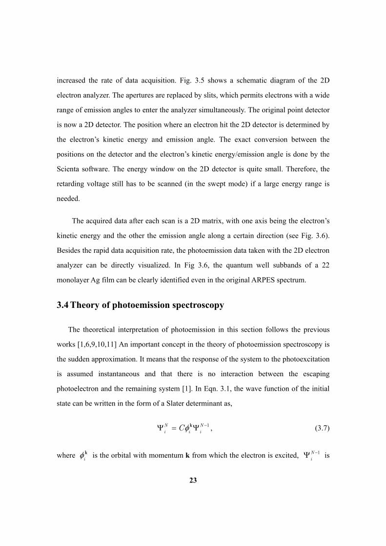
23
increased the rate of data acquisition. Fig. 3.5 shows a schematic diagram of the 2D
electron analyzer. The apertures are replaced by slits, which permits electrons with a wide
range of emission angles to enter the analyzer simultaneously. The original point detector
is now a 2D detector. The position where an electron hit the 2D detector is determined by
the electron’s kinetic energy and emission angle. The exact conversion between the
positions on the detector and the electron’s kinetic energy/emission angle is done by the
Scienta software. The energy window on the 2D detector is quite small. Therefore, the
retarding voltage still has to be scanned (in the swept mode) if a large energy range is
needed.
The acquired data after each scan is a 2D matrix, with one axis being the electron’s
kinetic energy and the other the emission angle along a certain direction (see Fig. 3.6).
Besides the rapid data acquisition rate, the photoemission data taken with the 2D electron
analyzer can be directly visualized. In Fig 3.6, the quantum well subbands of a 22
monolayer Ag film can be clearly identified even in the original ARPES spectrum.
3.4 Theory of photoemission spectroscopy
The theoretical interpretation of photoemission in this section follows the previous
works [1,6,9,10,11] An important concept in the theory of photoemission spectroscopy is
the sudden approximation. It means that the response of the system to the photoexcitation
is assumed instantaneous and that there is no interaction between the escaping
photoelectron and the remaining system [1]. In Eqn. 3.1, the wave function of the initial
state can be written in the form of a Slater determinant as,
1N Ni i iC k , (3.7)
where ik is the orbital with momentum k from which the electron is excited, 1N
i is

24
the wave function of the remaining (N-1) electrons and C is the operator that
antisymmetrizes the wave function. The wave function of the final state under the sudden
approximation can be written as a product of the wavefunction of the photoemitted
electron f
k and that of the remaining (N-1) electrons 1N
f,
1N Nf f fC k , (3.8)
Therefore, the matrix element in Eq. (3.1) is obtained as
1 1int ,
N N N Nf i f i f iH M k , (3.9)
where int ,f i f iH M k k k is the one-electron matrix element, and the second term is
the (N-1)-electron overlap integral. In the first step of evaluating the overlap integral, one
can assume that the remaining orbitals are the same in the final state as they were in the
initial state (frozen-orbital approximation), meaning that 1 1N Nf i . This renders the
overlap integral unity, and the transition matrix element is just the one-electron matrix
element. Under this assumption, the photoemission experiment probes only the
one-electron state (from i
k to f
k ) which does not interact with the remainder of the
(N-1) electrons. Of course, this cannot be a very good approximation.
In reality this simple picture breaks down because the excitation of an electron
from ik disturbs the remaining (N-1) electrons. The remaining system will readjust
itself in such a way as to minimize its energy (relaxation). We now assume that the final
state with (N-1) electrons has many possible excited states (labeled by s) with wave
function 1
,
N
f s and energy 1N
sE . Therefore, the total photoemission intensity measured
as a function of electron kinetic energy at a momentum k is

25
2 2 1
kin ,,
( , ) ( )N N
f i s K s if i s
I E M c E E E hvkk , (3.10)
where 22 1 1N N
s s ic is the probability that the removal of an electron from
the initial state k from the N electron ground state will leave the (N-1)-electron system in
the excited state s. For strongly correlated systems, many of the cs will be nonzero
because the removal of the photoelectron results in a strong change of the system’s
effective potential and, in turn, 1Ni
will overlap with many of the eigenstates 1Ns
.
Thus, the ARPES spectrum will not be a single delta function, but will instead show a
main line and several satellites according to the number of excited states s created in the
process.
The term 2 1( )N N
s K s is
c E E E hv in Eq. (3.10) is essentially the
one-particle spectral function. To see this, the wave function 1Ni can be expressed as
1N Ni ic k , where ck is the annihilation operator for an electron with wave vector k.
This term can be rewritten as
k 2
1 1( )N N N N
s i s is
c E E . (3.11)
This is exactly the spectral function with wave vector k and energy K
hv E . For a
2D single-band system, one can write the intensity measured in an ARPES experiment as
0
( , ) ( , , ) ( ) ( , )I I v f Ak k A k , (3.12)
where k=k// is the in-plane electron momentum, ω is the electron energy with respect to

26
the Fermi level, and 0( , , )I vk A is proportional to the squared one-electron matrix
element 2
,f iM k , which depends on electron momentum k, and on the energy and
polarization of the incoming photon. ( )f is the Fermi-Dirac function, which accounts
for the fact that photoemission probes only the occupied electronic states. ( , )A k is
the spectral function. Therefore, Eq. (3.12) shows that the photoemission intensity is
essentially the product of the squared matrix element 0( , , )I vk A and the spectral
function of the electron. For many 2D systems, 0( , , )I vk A is a slowly varying function
of electron momentum and photon energy, and therefore can be viewed as a constant
within a small momentum and energy space. In these cases, photoemission directly
probes the spectral function.
The spectral function is of crucial importance for understanding many-body
physics. The spectral function is directly related to the Green’s function as
Im{ ( , )}
( , )G
Ak
k . (3.13)
In a correlated electron system, the Green’s function is described in terms of the electron
self-energy ( , )k . The real and imaginary parts of the self-energy contain all the
information about the energy renormalization and lifetime of an electron with band
energy k and momentum k. The Green’s function can be expressed as
1( , )
( , )G
k
kk
. (3.14)
The corresponding spectral function is

27
2 2
1 Im ( , )( , )
[ Re ( , )] [Im ( , )]A
k
kk
k k. (3.15)
Note that k
is the bare band energy of the electron, assuming there is no
electron-electron correlation. It is obvious from Eq. (3.15) that the resulting spectral
function is a Lorentzian function.
When there is no interaction between the electrons, i.e., ( , ) 0k , the spectral
function is a delta function at k. If the electron-electron correlation is adiabatically
switched on, the system remains at equilibrium. However, any electron added into a
Bloch state has a certain probability of being scattered out of it by a collision with
another electron, leaving the system in an excited state in which additional electron-hole
pairs have been created. The result of this electron-electron correlation is that the energy
and lifetime of the electrons are changed. The slightly modified electron (with normalized
mass), described by Eq. (3.15), is generally called a quasiparticle. One can view this
quasiparticle as an electron dressed by virtual excitations that move coherently with the
electron through the crystal. In a correlated electron system, the spectral function is a
Lorentzian function, with its center and width determined by the energy and lifetime of
the quasiparticle, respectively.
Photoemission which probes the spectral function of the electron can be used to
study the quasiparticle dynamics in correlated electron systems. The peak positions and
linewidths are directly related to the electron self-energy, which makes ARPES a
powerful tool for studying many-body physics. It should be noted that the above
derivation is generally carried out for 2D electron systems where the spectral function
primarily determines the spectrum features. For 3D electron systems, the one-electron
matrix element could play the dominant role instead.

28
Photoemission spectra measured at various photon energies effectively probe the
electronic states with different k s. The reason is as follows: the energy conservation
(Eq. (3.1)) requires that the photoexcited electron gains the energy of the incoming
photon hv . In addition, the dipole transition term in (3.2), A p preserves the crystal
momentum of the electron during photoexcitation. Therefore, the photoexcitation caused
by the dipole transition term is a direct optical transition [3]. In the case of a
three-dimensional crystal, the direct transition can only occur at a specific k for a
given photon energy (See Fig. 3.7(b)). As the photon energy is swept, electronic states
with different k is probed accordingly. This photon energy dependence is
demonstrated in Fig. 3.7 (a) as the displacement of the direct transition peak at different
photon energies. In order to investigate the dispersion along the kz direction,
photoemission spectra must be taken at various photon energies. If the quasiparticle peak
positions do not move when the photon energy is varied, there is no dispersion along the z
direction.
As mentioned in Sec. 3.2, the contribution from the A term is not necessarily
small, especially near the surface. The dielectric discontinuity near the surface gives rise
to an abrupt change in A , which, upon differentiation, yields a delta function at the
surface [3]. As a result, the matrix element between the initial and final states
f i k k A is generally nonzero provided that both states have non-zero amplitude at
the surface. The contribution from this surface term to the transition matrix element is
proportional to the product of the amplitudes of the wavefunctions at the surface, namely,
0 0
* ( ) ( )f i
C z zk k , where 0z denotes the surface position. The coefficient C is
approximately proportional to the difference between the internal and external fields,
namely, ( 1)A , where is the dielectric constant of the material. The resulting

29
spectral contribution from this surface term generally resembles the one-dimensional
joint density of states.
Surface transition has been observed in many cases among which is the normal
emission spectrum of the Ag(111) surface as shown in Fig. 3.8. The direct transition peak
from the Ag sp bulk band exhibits a pronounced asymmetry with a long tail extending to
higher energy. This asymmetry arises from the spectral contribution of the surface
transition term which resembles the density of valence states. In general, the dipole
transition term dominates in photoemission when direct transition is allowed and surface
transition gives rise to only a small modification to the lineshape of the direct transition
peaks. However, when the direct transition is forbidden by certain selection rules, surface
transition will play a dominant role in the photoemission spectrum.
References:
[1] S. Hüfner, Photoelectron Spectroscopy, (Springer-Verlag, New York, 1996).
[2] H. J. Levinson, E. W. Plummer and P. J. Feibelman, Phys. Rev. Lett. 43, 952 (1979).
[3] T. Miller, W. E. McMahon and T.-C. Chiang, Phys. Rev. Lett. 77, 1167 (1996).
[4] W. Spicer, Phys. Rev. 112, 114 (1958).
[5] E. Rotenberg, 2001 Berkeley-Stanford Summer School Lecture (2001).
[6] A. Damascelli, Z. Hussain, and Z.-X. Shen, Rev. Mod. Phys. 75, 473 (2003).
[7] G. Somorjai, Chemistry in Two Dimensions: Surfaces (Cornell University Press,
Ithaca, 1981).
[8] H. Lüth, Solid Surfaces, Interfaces and Thin Films (Springer, 4ed, 2001).

30
[9] W. Schattke and M. A. Van Hove, Solid-State Photoemission and Related Methods:
Theory and Experiment (Wiley-VCH, 2003).
[10] E. W. Plummer and W. Eberhardt, Advances in Chemical Physics 49, 533 (1982).
[11] Y. Liu, Angle-resolved photoemission studies of two-dimensional electron systems,
Ph.D. thesis, University of Illinois at Urbana-Champaign (2010).

31
Figures:
Figure 3.1. A schematic showing the angle-resolved photoemission geometry. hv is the
incoming photon energy, and θ is the polar emission angle.

32
Figure 3.2. The photoemission process based on the three-step model [5].

33
Figure 3.3. Universal curve of the mean free path for inelastic scattering of electrons in a
solid [7].
34
V
R1
R2
R0
Detector
Lens
Vr
α
Hemisphere electron energy analyzer
Sample
Retarding
Aperture
Aperture
Figure 3.4. Schematic of a hemisphere electron energy analyzer.

35
Figure 3.5. Schematic of a 2D electron analyzer.

36
Figure 3.6. Original photoemission spectrum taken from a 22 ML Ag film on Si(111)
along M direction.
Bind
ing
Ener
gy (e
V)FE
3.0
1.0
2.0
Emission Angle (deg)
0 10 201020

37
Figure 3.7. (a) Normal emission spectra from Ag(111) taken with photon energies of 7, 8,
and 9 eV as indicated. (b) Band structure of Ag along the [111] direction. The horizontal
axis is the wave vector normalized to the distance between the zone center and the zone
boundary. Direct transitions for photon energies of 7, 8, and 9 eV are indicated by vertical
arrows [3].
(a) (b)

38
Figure 3.8. Surface transition in Ag(111) [3]. Top: a model fit (curve) to the normal
emission spectrum (circles) of Ag(111), taking into account both the dipole transition and
surface transition. Middle: spectral contribution from the dipole transition term. Bottom:
the density of valence states.

39
4 Theoretical Background
4.1 Introduction
This chapter provides the necessary theoretical background for understanding the
works reported in this thesis. Surface states, quantum well, Rashba effect and topological
order are the key concepts in the discussion of topological thin films and the Bi/Ag
surface alloy with a giant spin splitting, and those concepts are introduced in Sec. 4.2-4.5.
Sec. 4.6 will present a brief introduction to the calculation method employed in this
dissertation: density functional theory (DFT).
4.2 Surface states
The termination of a material with a surface not only gives rise to the surface
relaxation and reconstruction, but also strongly modifies the electronic structure at the
surface. Breaking of the lattice periodicity allows the existence of new states beyond the
Bloch bulk states. The wavefunctions of those new states are localized near the surface,
and thus they are accordingly termed surface states [1]. Their energy levels are found in
the band gaps where bulk states are not allowed. Intuitively the surface states can be
viewed as electronic states which are trapped by the band gap on one side of the surface
and the surface barrier potential, which prevents electrons from escaping into the vacuum,
on the other side.
Although the surface states are confined in the surface normal direction, they may
well delocalized in the two dimensions parallel to the surface. This can lead to the
formation of two-dimensional energy bands in the surface Brillouin zone (SBZ), k . In

40
order to examine the behavior of surface electrons, one needs to compare the surface
bands with the bulk bands projected to the surface [2]. Fig. 4.1 gives such a comparison.
Suppose the bulk band disperse along k , the wavevector perpendicular to the surface,
in the manner as shown in the left upper panel of Fig. 4.1. The width of this band then
gives the continuum of allowed states in the surface reciprocal space, and the projected
bulk bands are widened to have the shape of, say, the hatched area along a particular k
direction. Surface states may exist in the gap of the projected bulk bands as shown in the
upper middle panel. In such a case, the states must be localized near the surface as they
are not allowed in the bulk. Thus the wavefunctions of the surface states decay rapidly
towards the interior of the solid as illustrated in the lower middle panel. If, however, a
surface band stays in the band gap for only a limited range of k and overlaps with the
projected bulk bands for other k , as shown in the right upper panel, then the
wavefunction will be gradually evanescent towards the bulk as shown in the right lower
panel. These states inside the bulk band region are called surface resonance states. Both
surface state and surface resonance are experimentally observable by photoemission
spectroscopy, but a clear discrimination between the two is not always accessible. Fig. 4.2
shows projected bulk band structure (hatched area), surface states (solid curves) and
surface resonances (dashed curves) for three ideal silicon surfaces [3]. The Ag(111)
surface has a surface state at the zone center very close to the Fermi level, see the ARPES
spectrum of the Ag (111) film in Fig. 3.6.
4.3 Quantum well states
If the film thickness is comparable to the coherence length of the electron, the
electrons can bounce back and forth between the two boundaries of the film and form
electronic standing waves, known as quantum well states (QWS). For thin films,

41
quantum well states are often the dominant features, giving rise to quantum size effects.
The situation in the film normal direction is just like a 1D quantum box (Fig. 4.3(a)). The
allowed momenta along the z direction are discrete and depend on the film thickness and
boundary conditions (Fig. 4.3 (b)). As a consequence, the continuum of the valence band
is quantized in the kz direction (Fig. 4.3 (c)). Considering the dispersion along the kx and
ky directions, say, free-electron like, the band structure of the thin film will consist of a set
of parabolic quantum well subbands (Fig. 4.3(d)).
Calculating the QWSs in a rigorous manner requires solving the Schrődinger
equation for the whole film-substrate system. This can be achieved by means of the
modern first-principles method. The band structure of a 20 ML freestanding Ag(111) film
is shown in Fig. 4.4. The parabolic quantum well subbands are derived from the sp
valence orbitals of Ag while the densely packed flat bands are from the d orbitals of Ag.
The quantum well states of thin films can be readily examined by ARPES as shown
previously in Fig.3.6.
A much simpler way to interpret the QWS is given by the analogy between QWS
and the Fabry-Pérot interferometer [4]. In this phenomenological picture, QWS is formed
by multiple reflections of electron between the two confining boundaries (Fig. 4.5).
Therefore, electron waves are modulated by an interference factor
1
1 exp[ (2 )]exp( / )s i s ir r i kNt Nt
, (4.1)
where rs and ri are the reflectivities at the surface and the interface, respectively, k is the
electron wave vector, N is the film thickness in monolayers, t is the monolayer thickness,
Φs and Φi are the phase shifts at the surface and interface, and λ is the quasiparticle mean
free path. The photoemission intensity is proportional to the absolute square of the factor
in Eqn. 4.1. Thus, the photoemission spectrum for a quantum well becomes

42
22
2
1
41 sin ( )
2s i
If
kNt
, (4.2)
where f is the Fabry-Pérot finesse (ratio of the peak separation to the peak width) given
by [5]
exp( / 2 )
1 exp( / )i s
i s
r r Ntf
rr Nt
. (4.3)
Eqn. (4.2) yields a set of peaks at positions where the sine function in the denominator
equals zero, and the resulting condition is just the Bohr-Sommerfeld quantization rule
2 ( ) ( ) ( ) 2i s
k E Nt E E n . (4.4)
The quantization condition states that the accumulated phase shift after a round trip
should be an integer of 2π. The peak width E is
1 exp( 1/ )
exp[ 1/ (2 )]s i
s i
r rE
r r
, (4.5)
where Γ is the quasiparticle inverse lifetime which is related to the group velocity ν by
Γ=ν/λ, and η= λ/(Nt). The quantities k and Γ (related to the real and imaginary parts of the
electron self-energy) as well as r and Φ (related to the confinement potential) are of basic
interest and completely determine the interferometer properties. While k and Φ determine
the peak positions through Eq. (4.4), Γ and r control the peak width through Eq. (4.5).
They all depend on the electron energy E, but not on the film thickness N. The
Fabry-Pérot analysis of QWS has proven to be very successful for explaining many
phenomena related to QWS. For example, the normal emission curves taken from Ag
films on Fe(100) have been perfectly fitted using the Fabry-Pérot solutions.
Generally, the electron wave vector k and group velocity ν as a function of energy
are derived from the bulk band structure. The reflectivity at the surface, rs, should be
unity. The reflectivity at the interface, ri, depends on the interface potential and the
43
electron energy. The phase shifts, Φi and Φs, are related to the logarithmic derivatives of
the wave functions at the boundaries. The electron mean free path is normally much
larger than the film thickness (for sp electrons). Therefore, Eq. (4.5) can be simplified as
1
i
i
rE
Nt r
. (4.6)
The substrate modifies the QWS energy positions and the peak widths, through the
reflectivity and phase shift at the interface (Eqns. (4.4) and (4.5)). When ri is less than 1,
the QWS becomes a quantum well resonance because the wave function penetrates into
the substrate and forms a resonant state.
When the Fermi wave vector kF is not at the zone boundary like the case shown in
Fig. 4.3(c), the QWS crosses the Fermi level periodically as the film thickness N varies
according to Eq. (4.4). The periodicity is simply
/( )F
N k t . (4.7)
This periodic crossing of QWS at the Fermi level brings about an oscillation of the
density of states (DOS) at the Fermi level as a function of N. Since the DOS at the Fermi
level is closely related to many physical properties such as resistivity, superconducting
transition temperature, thermal stability, etc., these physical properties are expected to
exhibit oscillating behavior when the film thickness varies [6].
4.4 Rashba effect
The Rashba effect is a momentum dependent spin splitting of electronic bands in
two dimensional condensed matter systems (heterostructures and surface states) [7]. This
spin splitting effect is a combined effect of atomic spin-orbit coupling and space
inversion asymmetry (SIA) caused by the potential in the direction perpendicular to the
two-dimensional plane. The essential physics can be easily seen in a simple model of an

44
ideal 2D electron gas propagating in the vertical electric field 0E z E . Due to
relativistic corrections an electron moving with velocity v in the electric field will
experience an effective magnetic field B,
2/ c B v E , (4.8)
where c is the speed of light. This magnetic field couples with the electron spin
2
( )2
BSOH
c v E , (4.9)
where the factor 1/2 is a result of the Thomas precession and are Pauli matrices.
Within this simple model, the Rashba Hamiltonian is given by
( )R RH z p , (4.10)
where 022
BR
E
mc .
The band structure of the ideal 2D electron gas with Rashba spin splitting around the
point ( k =0) of the surface Brillouin zone is shown in Fig. 4.7 [8]. A cut along an
arbitrary direction through gives a characteristic dispersion of two split parabolas,
2 2 22
0 0 0( ) ( )2 2B
kE E k E k k
m m
k , (4.11)
where 20 /Rk m is the momentum offset of the band maximum and m is the
effective mass which is negative in this case. The band dispersion can be divided in two
qualitatively different region. If E lies below E0, in region II, the constant energy contour
consists of two circles of opposed spin helicities and the density of states (DOS) does not
differ from that of the case without the SOC. If E is above E0, in region I, the two circles
have identical helicity and the DOS switches to a 1 / E behavior.
The Rashba model in solids can be derived in the framework of the k p theory

45
[9] or from the point of view of a tight binding approximation [10]. However, the specific
calculations are quite tedious. The intuitive model gives qualitatively the same
physics given a good estimate of the Rashba parameter R . A more detailed discussion
on the Rashba effect will be presented in Chapter 8.
4.5 Topological insulator and topological order
Topological insulator is a fundamentally new phase of electronic matter that has
captured a lot of research interest over past several years. Topological insulators exhibit a
rare type of behavior called topological order which describes the organized movement of
the electrons in the crystal. There have been many excellent review articles on topological
insulators [11,12]. Here we only present an intuitive physical picture which can be
directly tested by ARPES measurements. A consequence of the topological order is that
the surface electron spectrum of a topological insulator is qualitatively distinct from any
ordinary material in such a way that it allows surface electrons flow without being
scattered by impurities. In an ordinary insulator with spin-orbit coupling, there can be
spin-polarized surface states that span the bulk energy gap as shown in Fig. 4.8. For
ordinary insulators these surface states always disperse such that they form even number
Fermi surface contours around time reversal invariant momenta (TRIM, k1 and k4 in Fig.
4.8). In topological insulator, however, the number of Fermi surface contours is odd. This
even or odd count is a topological distinction and it's obvious that this method of
counting relies on the fact that the material is a bulk insulator. Because of the opposite
spin orientations in the two branches of the surface band, the backscattering of surface
electrons is not allowed in the topological insulator and the overall gapless connection
pattern of surface states to the bulk bands is protected as a subtle consequence of the time
reversal symmetry.
Our group has successfully fabricated the topological insulator Bi2Te3 thin films of

46
high structural quality [13]. The ARPES spectra taken from those topological thin films
are shown in Fig. 4.9 in which the quantum well states (QWS) and topological surface
states (TSS) are clearly mapped out. The QWSs with energies between about –0.4 to –0.6
eV split into more and more subbands as the film thickness increases from 2 to 5 QLs.
These layer-resolved QWSs provide a means to accurately calibrate the exact thickness of
each film. The V-shaped TSS band spanning the whole bulk band gap and the single
hexagonal constant energy contour around the zone center point unambiguously
demonstrate the nontrivial topological order of Bi2Te3. More discussion on topological
insulator and topological order can be found in Ch. 5 and Ch. 6.
4.6 Density functional theory
The first-principles calculation employed in this thesis are based on density
functional theory (DFT) which is a quantum mechanical modeling method used in
physics and chemistry to investigate the electronic structure of many-body systems such
as atoms, molecules, and the condensed matters. Within this theory, the properties of a
many-electron system can be determined by a functional of the spatially
dependent electron density [14 ,15]. The DFT approach is to replace the difficult
interacting many-body system with an auxiliary non-interacting system that can be solved
more easily [16]. This leads to independent-particle equations for the non-interacting
system that can be considered soluble by numerical means with all the difficult
many-body terms incorporated into an exchange-correlation functional of the density. The
calculation accuracy is limited only by the approximations in the exchange-correlation
functional.
For a non-interacting system, the ground state can be written in the form of a Slater
determinant as,

47
1
( ) ( )N
ii
Cr r , (4.12)
where i is the one-particle wavefunction and C is the operator that antisymmetrizes
the wave function. The density of the auxiliary system is given by sums of squares of the
orbitals for each particle
2
1 1
( ) ( ) ( )N N
i ii i
n n
r r r . (4.13)
The independent-particle kinetic energy is given by
22
1 1
1 1( )
2 2
N N
i i ii i
T dm m
r r , (4.14)
and the classical Coulomb interaction energy of the electron density n(r) interacting with
itself is defined as
1 ( ) ( )[ ]
2Hatree
n nE n d d
r r
r rr r
. (4.15)
The ground state energy functional for the auxiliary non-interacting system can be
expressed in the form
[ ] ( ) ( ) [ ] [ ]DFT ext Hatree II XCE T n d V n E n E E n r r r , (4.12)
where Vext (r) is the external potential due to the nuclei and any other external fields, EII is
the interaction between the nuclei and EXC is the exchange-correlation functional of the
density. Solution of the auxiliary system for the ground state can be considered as the
problem of minimization with respect to the density n(r). The Schrodinger -like equation
for each particle can be derived by varying the ground state energy functional EDFT,
( ) ( ) 0DFT i iH r , (4.13)
where i are the eigenvalues, and HDFT is the effective Hamiltonian,

48
21( ) ( )
2DFT DFTH V r r , (4.14)
with
( ) ( ) ( ) ( ) ( )( ) ( )
Hatree XCDFT ext ext Hatree XC
E EV V V V V
n n
r r r r r
r r. (4.15)
The solution of the independent-particle equations, Eqn. (4.13), must be found
self-consistently with the resulting density as shown in the diagram of Fig. 4.10. These
equations are independent of any approximation to the functional EXC[n], and would lead
to the exact ground state density and energy for the interacting system, if the exact
functional EXC[n] were known.
The major problem with DFT is that the exact exchange and correlation functionals
are unknown except for the free electron gas. However, approximations have been found
which permit the calculation of physical quantities in many cases quite accurately. In
physics the most widely used approximation is the local-density approximation (LDA),
where the functional depends only on the density at the coordinate where the functional is
evaluated,
[ ] ( ) ( )LDAXC XC
E n d n n r r , (4.16)
where ( )n is a function, rather than a functional, of the density n. Another popular
approximation is the generalized gradient approximation (GGA). GGA is still local like
LDA but also take into account the gradient of the density at the same coordinate,
[ ] ( , ) ( )GGAXC XC
E n d n n n r r . (4.17)
In this thesis, LDA is mostly employed for the first-principles calculations while there are
situations where GGA is used to test the robustness of the calculation results.
The density functional theory could not have been so successful without the
development of modern pseudopotentials. The pseudopotential theory is based on the fact

49
that many properties like conductivity and chemical bondings are governed only by
valence electrons, with core electrons being inert. Pseudopotentials replace the strong
Coulomb potential of the nucleus and the effects of the inert core electrons by an
effective ionic potential acting on the valence electrons. This reduces, sometimes
drastically, the number of electrons needed to solve. Even more importantly, this results
in much smoother wave functions for the remaining valence electrons, making the
problem much easier to solve numerically. The pseudopotential approach reduces greatly
the computational power required for DFT calculations, making considerably complex
tasks manageable even on desktop computers. A description of the software and
pseudopotentials employed for our first-principles calculations will be given in Appendix
A.
References:
[ 1 ] S. G. Davison and M. Steslicka, Basic Theory of Surface States (Clarendon
Press,1992).
[2] X. Ding, X. Yang and X. Wang, Surface Physics and Surface Analysis (Fudan
University Press, 2004).
[3] A. Zangwill, Physics at Surfaces (Cambridge University Press, 1988).
[4] J. J. Paggel, T. Miller, and T.-C. Chiang, Science 283, 1709 (1999).
[5] M. Born, and E. Wolf, Principles of Optics (Pergamon, New York, ed. 6, 1980).
[6] T.-C. Chiang, Science 306, 1900 (2004).
[7] Y. A. Bychkov and E. I. Rashba, J. Phys. C 17, 6039 (1984).

50
[8] L. Moreschini et al., Phys. Rev. B 80, 035438 (2009).
[9] R. Winkler, Spin-orbit Coupling Effects in Two-Dimensional Electron and Hole
Systems (Springer, New York, 2003).
[10] L. Petersen and P. Hedegård, Surface Science 459, 49 (2000).
[11] M. Z. Hasan and C. L. Kane, Rev. Mod. Phys. 82, 3045 (2010).
[12] X. L. Qi and S. C. Zhang, Rev. Mod. Phys. 83, 1057 (2011).
[13] Y. Liu, G. Bian, T. Miller, M. Bissen and T.-C. Chiang, Phys. Rev. B 85, 195442
(2012).
[14] P. Hohenberg and W. Kohn, Phys. Rev. 136, B864 (1964).
[15] W. Kohn and L. J. Sham, Phys. Rev. 140, A1133 (1965).
[16] R. Martin, Electronic Structure: Basic Theory and Practical Methods (Cambridge
University Press, 2008).

51
Figures:
Figure 4.1. Schematic illustration of the surface states as compared with the projected
bulk bands (the hatched area) [2]. Left: projected bulk bands and a bulk state. Middle: a
surface band (the solid line) and a surface state. Right: a surface resonance. The “0”
denotes the surface position.
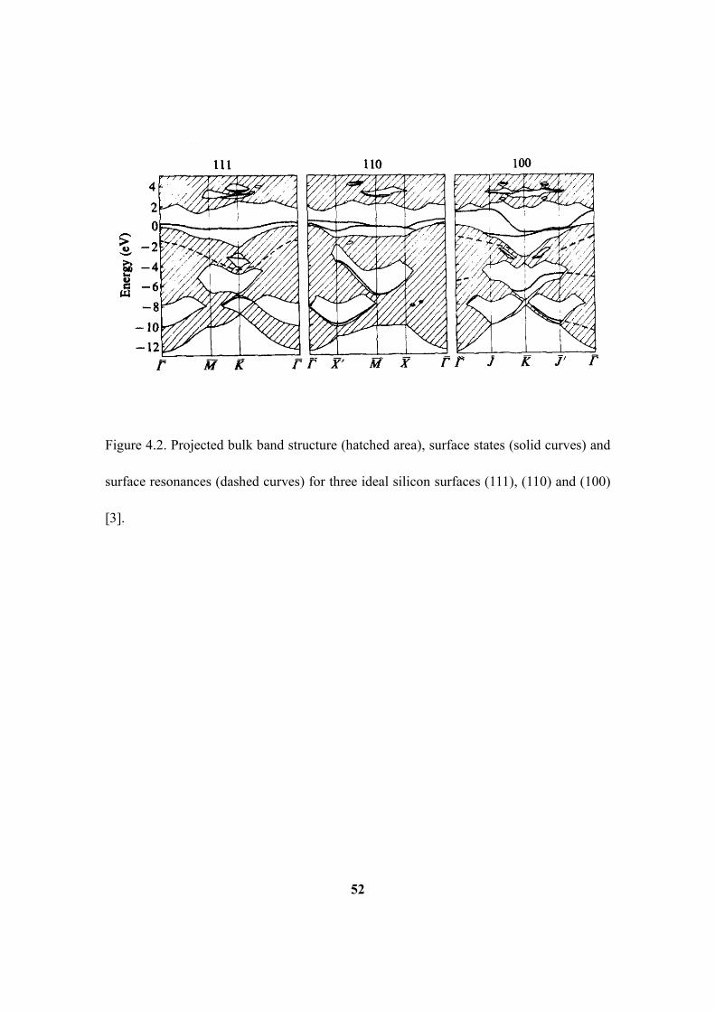
52
Figure 4.2. Projected bulk band structure (hatched area), surface states (solid curves) and
surface resonances (dashed curves) for three ideal silicon surfaces (111), (110) and (100)
[3].

53
Figure 4.3. (a) quantum well states in a 1D quantum box. (b) Allowed electronic states in
momentum space for a free-electron-like thin metal film. (c) Discretization of the
continuum of the valence band. (d) Band dispersion relations of free-electron like
quantum well subbands.
(d)
(b)
(c)(a)
Fk
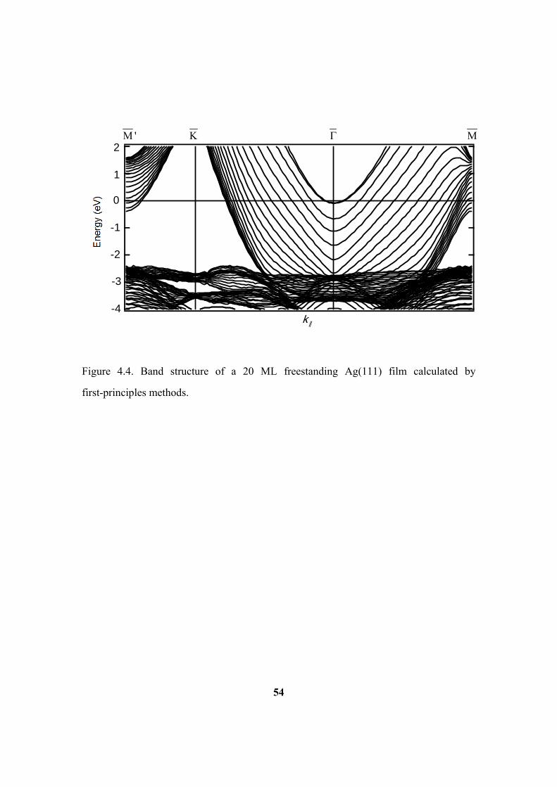
54
Figure 4.4. Band structure of a 20 ML freestanding Ag(111) film calculated by
first-principles methods.
MM ' K
0
-1
-2
-3
-4
1
2
∥k

55
Figure 4.5. Schematic of a thin film as a Fabry-Pérot interferometer. The initial state
undergoes multiple reflections to form QWS. After photoexcitation, the electron is
emitted from the film as a time-reversed LEED state.
Substrate
Vacuum
Emission
kFilm
( , )S Sr
( , )I Ir

56
Figure 4.6. Experimental quantum well states for Ag films on Fe(100) taken with
16 eVh radiation [4].

57
Figure 4.7. Schematic of the band dispersion with Rashba splitting [8]. The crossing point
at defines two different regions: region I, where the constant contours have the same
helicity and the DOS follows a 1 E behavior, and region II, where the two contours
have opposite helicities and the Dos is constant as in a conventional 2D electron gas.

58
Figure 4.8. Schematic of Fermi surface contours and surface bands of an ordinary
insulator (Left) and a topological insulator (Right).
Non-topological Topological

59
Figure 4.9. (a) Photoemission spectra of 2- through 5-QL Bi2Te3 films measured along the
ΓM direction, using 31-eV photons. Green curves are band dispersions extracted from
data. (b) Constant energy contours at 0.28 eV above the Dirac point for the same set of
films, taken with 26-eV photons. Green curves are best fits to the experimental data. [13]

60
Figure 4.10. Schematic representation of the self-consistent loop for solution of
Kohn-Sham equations [16].

61
5 Topological Sb Thin Films
5.1 Introduction
Topological insulators are characterized by a strong spin-orbit coupling that leads
to a set of spin-split surface states with special connections to bulk states [1,2,3,4,5,6,7,8].
In the simplest case where just one pair of spin-split surface states exist in the gap, one of
them must disperse into the bulk conduction band, and the other must disperse into the
bulk valence band. The bulk gap is thus completely spanned by metallic surface states
that carry a net spin current. Whereas the surfaces of bulk topological insulators provide a
promising basis for spintronics applications for this reason, thin films are more relevant
to actual device architecture. In this chaper we examine the mesoscopic regime where the
film thickness is sufficiently large to retain the characters of the spin-polarized surface
states, while the bulk continua are replaced by densely populated, but experimentally
resolvable, quantum well states that are spin-unpolarized in centrosymmetric cases [9].
The surface states now must disperse and connect to the quantum well states and
therefore lose their spin polarization in the process by bulk symmetry requirements. The
nature of this passage, relevant to spin transport and relaxation in the ballistic regime, is
the focus of this Chapter.
When topological films become ultrathin, the surface states on the two faces of the
film can overlap and interact by quantum tunneling of the surface electrons between the
two faces. The coupling breaks the degeneracy at the Dirac point, resulting in a gap
[10,11]. This gap precludes electrical transport and can be detrimental to device
performance, but it is a subject of great interest in connection with the search for
Majorana states and other exotic emerging properties [12]. The size of the gap and the

62
underlying interaction are issues of central importance in the physics and applications of
topological films, which are the subject matters of the second part of this chapter.
5.2 Experimental preparation of Sb films
We choose a simple model system, Sb films, for two reasons. Firstly, the semimetal
Sb shares the same topological order as Bi1-xSbx (0.07 < x < 0.2) [5,13], the first material
identified as a three-dimensional topological insulator [14]. Sb possesses a pair of
Rashba-type spin split surface bands within its bulk band gap. Unlike other Rashba
systems such as Au films [13], the two surface bands in Sb are connected to the
conduction band and the valence band separately. The resulting gapless configuration of
the surface bands gives rise to a single Dirac cone, which is the signature of nontrivial
topological order. Secondly, recent studies of Bi films [15] also show entanglement
between the surface states and quantum well states and merit a comparison. However, Bi
is topologically trivial; it has a more complicated band structure involving mixing of
surface and bulk bands near the zone center [16,17]. The complexity impedes a
straightforward demonstration of the passage from the spin polarized surface states to
quantum well states. Sb films present a much simpler case.
The spin-split surface states of bulk Sb samples have been studied by angle-resolved
photoemission (ARPES) before, but these states are observable only near the surface zone
center [18,19,20,21]. From the fabrication standpoint, making smooth thin films that
preserve the surface spin properties presents a technical challenge. Through
experimentation, we have found that Sb films grown on the usual Si(111) substrates are
rough. Instead, we first prepared a Bi buffer layer (or a Bi-terminated
Si(111)- 3 3 30R surface) on the Si(111) substrate to support the growth of
ultrasmooth Sb films. An n-type Si(111) wafer (Sb-doped with a resistivity of ~0.01

63
cm ) was cleaned by direct current heating to yield a (77) reconstructed surface. It
was cooled to 60 K, and about 60 Å of Bi was deposited on top. The sample was then
annealed at 400 K to smoothen the Bi film. This Bi covered substrate was used as the
substrate for Sb film growth. The deposition of Sb was performed at 60 K; subsequently,
the film was annealed to 450 K to form a well ordered Sb film. Bulk Sb has the
rhombohedral A7 crystal structure, which is essentially a distorted fcc NaCl structure
[22,23]. Films of Sb studied here are (111)-oriented and consist of a stack of bilayers
(BL), each of which resembles a buckled graphene sheet. The surface Brillouin zone is a
simple hexagon [19]. Fig. 5.1 shows the configuration of the sample, the atomic structure
of the Sb films, and the surface Brillouin zone.
5.3 Bulk band structure of Sb
The relationship between the bulk Brillouin zone of Sb and the surface Brillouin
zone along the [111] direction is shown in Fig. 5.2(a). The calculated bulk band structure
of Sb along the Γ-T and L-X directions are shown in Figs. 5.2(b) and 5.2(c),
respectively. Results from similar calculations, but with the spin-orbit coupling excluded,
are shown in Figs. 5.2(d) and 5.2(e), respectively. The nearly parabolic quantum well
subbands around the M point observed in ARPES from the Sb film can be attributed to
quantization of the nearly linear bulk bands along the X-L direction near the Fermi level.
The bundle of subbands that converge toward 0.5 eV near normal emission from the film
can be attributed to the nearly flat portion of the top valence band near the T point. The
main effect of turning off the spin-orbit coupling is to shift the band energies. A more
subtle effect is the introduction of nonzero Z2 topological numbers to the system.
Calculations show that Sb belongs to the nontrivial Z2 class of (1;111)[5].

64
5.4 Passage from spin polarized TSS to spin degenerate QWS
ARPES mapping along the M direction of the band structure of a 20 BL (~79
Å) Sb film reveals a rich structure of subbands as a function of the in-plane wave vector
kx, as seen in Fig. 5.3(a). Figure 5.3(b) shows the same data differentiated twice along the
energy axis. This differentiation effectively removes a background and enhances the
contrast for a better visualization of the band dispersions. For comparison, Fig. 5.3(c)
shows the results from a first-principles calculation; the film is assumed to be
freestanding for simplicity. Substrate effects including the modification of the surface
states at the interface (not observable by photoemission) and a possibly tiny splitting of
the quantum well subbands [24] are thus ignored here, but these do not affect our main
conclusions as discussed in [19].
Two bands that have been identified as surface states near the zone center in bulk
Sb are labeled A and B in Fig. 5.3(c). They are degenerate at the surface zone center ,
but separate in energy elsewhere by spin-orbit coupling because of the surface potential
gradient (Rashba effect). The shading in the figure indicates the bulk band continua
(thick-film limit). A gap separates the valence and conduction bands throughout the entire
zone, which makes Sb a semimetal. The calculated gap is somewhat smaller than the
experimental results [14]. For bulk Sb, the upper and lower surface states merge with the
conduction and valence bands, respectively, and are observable only near . In the film,
the bulk continuum is replaced by quantum-well states, and calculation shows these two
states remaining distinct all the way to the zone boundary at M . The solid curves in Fig.
5.3(e) indicate schematically the portions of the two states above the Fermi level based on
a comparison between theory and experiment. The dashed curve Q indicates the topmost
quantum well subband below states A and B. It serves as a reference for connecting the

65
two visible pieces of state B, which lie next above Q. Likewise, the two visible pieces of
state A in Fig. 5.3(e) are connected as they lie next above B. In bulk Sb, the states A and B
are not observed near the zone boundary by photoemission, but in the film they are seen
and should correspond to quantum well states, as verified by calculation (see below). The
M point is a special "time-reversal invariant" point in reciprocal space. The two states
remain separate in energy at M , which is a necessary, but not a sufficient, condition for
nontrivial topological order [4,14,19,25].
Quantum well states in freestanding Sb films are, however, spin-unpolarized,
because they are derived from bulk states that are invariant under time-reversal (T) and
space-inversion (or parity, P) operations. Thus, each quantum well state is doubly
degenerate relative to spin. The question is: how do the two spin-split surface states get
connected to spin-degenerate pairs of quantum well states across the band edges? An
important clue is revealed by turning off the spin-orbit coupling in the calculation (Fig.
5.3(d)), thus rendering the system topologically trivial. The subband structure and the
bulk gap remain largely unaffected, but the two surface states A and B become degenerate
within the gap. Each state A and B is additionally doubly degenerate because of the two
surfaces; the total degeneracy is thus four-fold. Outside the gap, the two connecting
quantum well states remain separate. Thus, the energy separation of the two quantum
well states is not a consequence of spin interaction. It must arise from differences in the
spatial parts of the wave functions that lead to different charge density patterns.
An explanation is offered by the schematic diagram in Fig. 5.4 that shows the
charge and spin characters of the surface states of a 20 BL Sb film. At the zone center,
there are four degenerate surface states; each of the two surfaces (left L and right R) of
the film contains two spin degenerate surface states. For each surface, the spin
degeneracy is lifted away from (Fig. 5.4(a)). Consider the four points on the

66
dispersion relations, A, A', B, and B', with 0.1 Mxk . Each surface state is
characterized by a decay length (Fig. 5.4(b)). The two states on the right surface, AR and
BR, are spin polarized in opposite directions, along –y and +y, respectively. They are
related to the two states on the left surface, AL and BL, by L RA A TP and L RB B TP .
For the two states on the same surface but with negative xk , the relationships are
R RA A T and R RB B T . The actual charge and spin distributions of the four states
from the calculation are presented in Fig. 5.4(c).
As xk increases, the surface states move toward the bulk band continua. Their
decay lengths increase as illustrated by the calculated plane-averaged charge densities for
a 20 BL Sb film (Fig. 5.5). Near the edges of the band gap, each pair of degenerate
surface states associated with the two surfaces (e.g., LA and RA ) begin to overlap
across the central plane of the film. They remain degenerate because of their opposite
spin orientations. However, the spatial overlap leads to a cancellation of the spin
polarizations. Eventually, they combine into a quantum well state pair, doubly degenerate
with respect to spin, and with a charge density distribution resembling a standing wave
bounded within the film. This manner of passage from surface states to quantum well
states allows the spin polarization to switch smoothly across the band edges. The
degeneracy of the two surface states associated with spatial separation (left and right
surfaces) evolves into spin degeneracy for the two quantum well states with identical
spatial wave functions.
With the spin-orbit coupling turned off in the calculation, the four states AR, AL, BR,
and BL are degenerate within the gap (Fig. 5.3(d)). They split into two spin-degenerate
pairs of quantum well states across the band edges, one pair derived from a mixture of AR
and AL, and the other from a mixture of BR and BL. The splitting can be understood in

67
terms of how the two surface states from the two surfaces interact in real space when
their decay lengths are long enough for them to overlap. The interaction leads to a mixing
that can be either in phase or out of phase, resulting in an antinode or node at the
midpoint of the film. The energy splitting is the usual even-odd splitting familiar from
surface state calculations for films that are sufficiently thin for the states associated with
the two surfaces to couple, and this mechanism applies only to states having the same
spin. The calculated charge density functions in Fig. 5.5 reveal the differences in the
nodal structures of the quantum well states.
The passage from surface states to quantum well states, with very different charge
distributions, can be characterized by the charge separation function defined below for
each of the two states A and B:
,
2| | 1x i x i x
i L R
C k k z kD
, (5.1)
where D is the film thickness, is the normalized charge density operator, z = 0 is at the
midpoint of the film, and the summation is for the two degenerate states associated with
the two surfaces. It ranges from 0 (uniform charge distribution) to 1 (charge concentrated
at the surfaces at z = ±D/2). The results from the calculation, presented in Fig. 5.6, show a
smooth transition across the band edges. Likewise, a spin separation function can be
defined:
,
2x i x y i x
i L R
S k k s z kD
, (5.2)
where sy is the spin operator along y, the only direction yielding a nonzero value based on
the Rashba effect [26]. This quantity is normalized to ±1 for a fully spin-polarized TP
pair concentrated at the two film surfaces, and its sign indicates the spin orientation of the

68
state on the right (positive z) surface. The calculated results in Fig. 5.6 show a transition
from oppositely polarized surface states at the two surfaces to unpolarized quantum well
states, with a trend of transition very similar to that of the charge separation.
For the ten quantum well states of a 20 BL Sb film at the surface zone boundary M
point indicated by circles in Fig. 5.7(a), we have computed the corresponding
plane-averaged charge densities; the results are shown in Fig. 5.7(b). For symmetry
reasons, the charge distribution for each state must be symmetric about the midpoint of
the film. It is either a minimum or a maximum there, and successive states derived from a
single band should alternate between the two cases. All of the ten states follow this rule,
except that there is a phase slip between the top two states; also, the top three states show
envelope functions that do not follow a simple pattern. These variations are caused by the
involvement of additional bulk bands within this energy range (Fig. 5.2).
We also mapped out the band structure of a 20 BL Sb film grown on a Bi-terminated
Si(111)- 3 3 30R surface, and the result is shown in Fig. 5.8. The role played by
the Bi buffer layer and the Bi-terminated Si(111)- 3 3 30R surface in the epitaxial
growth of Sb films is to smoothen the Si(111)-77 surface.
5.5 Quantum tunneling effect in ultrathin Sb films
As the Sb films become thinner, the semimetallic gap widens. Our first-principles
calculations show that the gap at a film thickness of 4 BL becomes slightly positive as
shown in Fig. 5.9, making the system insulating in the bulk. The green band bordered by
dashed lines indicates a +40 meV absolute band gap, defined as the gap between the top
valence quantum well subband and the bottom conduction quantum well subband. Within
this gap, there is a single crossing along M by the spin-polarized surface states.

69
Unlike the surface states, all quantum well subbands are spin unpolarized. The same
calculation shows a tunneling-induced gap of 36 meV at the Dirac point of the surface
states, an undesirable result. Surprisingly, angle-resolved photoemission spectroscopy
(ARPES) measurements of a 4-BL film grown on Si(111) reveal no such gap at the Dirac
point, even though the rest of the experimental band structure appears very similar to the
calculated one. The observed robust gapless Dirac cone is very promising for applications.
The puzzling difference between experiment and calculation is explained by additional
model calculations taking into account of the substrate.
Figure 5.10(a) presents calculated band structures of freestanding Sb films at various
thicknesses in the range of 1-10 BL along the M direction. The shaded areas
indicate the projected bulk band regions, and states within the bulk gap are of surface
character. The spin-split surface states begin to appear at a thickness of 2 BL, but there is
a fairly large tunneling-induced gap of 86 meV at . This gap diminishes as the film
thickness increases and essentially vanishes at ~8 BL when the gap becomes smaller than
thermal broadening. The calculated gap E as a function of thickness is shown in Figs.
5.10(b) and 5.10(c) using linear and logarithmic scales, respectively. The decay of the
gap beyond above about 6 BL is exponential; a fit to the asymptotic behavior yields a
decay length of about 1.1 BL, which characterizes the spatial extent of the surface state
wave function. The calculated plane-averaged charge densities of the lower surface state
at the zone center for a thick Sb(111) film and a 4-BL film are shown in Figs. 5.10(d) and
5.10(e), respectively. The surface state is mostly localized within the top BL. The small
tail allows the surface states associated with the two faces of the 4-BL film to overlap,
giving rise to the gap. The other bands in Fig. 5.10(a) are quantum well states in the film.
Unlike the surface states, the quantum-well states are spin degenerate. Another important
distinction is that the quantum-well bands become more numerous as the film becomes
thicker.

70
ARPES mapping of the band structure of a 4-BL Sb film is presented in Fig. 5.11(a).
The band dispersions are in fairly good accord with calculated ones presented in Fig.
5.11(b) for a freestanding 4-BL film. The data confirm the atomic-level uniformity of the
film; any significant admixture of 3- or 5-BL patches would give rise to additional
quantum-well bands. Similar comparison between experiment and theory for a 20-BL
film is presented in Figs. 5.11(c) and 5.11(d). The surface states are well resolved, but not
for the dense set of quantum well states at low energies. Despite the overall similarity, the
experiment and theory do differ in some details. Shown in Fig. 5.11(e) is a close-up view
of the experimental spin-split surface bands near the zone center for the 4-BL film; the
data contrast has been enhanced by taking the second derivative in energy. The
corresponding theoretical bands are shown in Fig. 5.11(f), with the bands suitably
broadened to simulate the data. The gap at the zone center, 36 meV in the calculation, is
absent in the data. The theoretical dispersion relations have noticeably higher energies.
It is interesting to note that prior studies of related systems such as Bi2Se3 thin films
have shown convincingly the presence of tunneling-induced gaps at small film
thicknesses [27]. Our observation here represents the first clear-cut case of a zero gap at a
film thickness where a sizeable gap is predicted. The difference can be attributed to the
boundary conditions specific to the interface bonding for each case. In our system, the
bottom face of the Sb film forms chemical bonds with the substrate surface. Since the
film and the substrate are incommensurate, an accurate theoretical modeling including the
substrate is not feasible. Instead, we simulate the effect of interfacial bonding by
terminating the bottom face of a 4-BL Sb film with H. The results of the calculation,
shown in Fig. 5.11(g), are in much better agreement with the experiment than the
freestanding case. Specifically, the gap becomes zero, and the energy positions of the two
surface bands are much closer to the experimental results. Thus, H-termination is a good
approximation for the interfacial bonding in our case. A similar case can be made for

71
Bi-termination. For comparison, data from the 20-BL film, presented in Fig. 5.11(h),
shows no gap, just as expected. The surface states have somewhat lower energies, in
agreement with the calculation shown in Fig. 5.11(d).
The absence of a gap at 4 BL can be understood as a result of the suppression of the
tunneling-induced coupling. The chemical bonding at the interface introduces a large
asymmetry in the film. The topological surface states at the interface undergo a large
energy shift and are no longer degenerate with the surface states at the top surface.
Quantum tunneling is thus turned off for lack of energy conservation, and the gap
disappears correspondingly. This effect should become more pronounced at smaller film
thicknesses. However, we have not been able to prepare atomically smooth films in the
1-3 BL range despite repeated attempts. Those films were rough probably due to an
inherent critical thickness of 4 BL for smooth growth.
To explore the nature of the tunneling interaction and interfacial coupling in detail,
we show in Figs. 5.12(a) and 5.12(c), respectively, the calculated band dispersion
relations for a freestanding 6-BL Sb film and for the same film with its bottom face
terminated by H. For an intermediate case involving a weak interfacial bonding, we
choose a model in which the bottom layer of the film is replaced by a mixture of Sb and
Bi, represented in the calculation using the average pseudopotential of Sb and Bi. The
rationale is that Sb and Bi are isoelectronic and chemically similar. The mixing is a good
approximation for a somewhat perturbed bottom layer caused by a weak interfacial
bonding. The results of the calculation are shown in Fig. 5.12(b). In Fig. 5.12(a), the two
surface bands show a tunneling-induced gap. In Fig. 5.12(b), the surface states on the
bottom face of the film are shifted slightly downward in energy by the interfacial
perturbation, resulting in two separate Dirac cones at the zone center. In Fig. 5.12(c), the
downward energy shift for the bottom surface states is so large that these states merge
into the quantum-well manifold, and only the pair of top surface states remains in the gap

72
with a zero gap at the Dirac point. The surface bands in Fig. 5.12(a) are doubly
degenerate because of the two surfaces of the film, while those in Fig. 5.12(c) are
non-degenerate.
The essential physics of the system can be further elaborated in terms of a four-band
Rashba model with the basis set {| ,| , | , | }T T B B , where is a surface
state, and T and B denote the top and bottom surfaces, respectively. The effective
Hamiltonian is
2
0 4 2 2 2( ) ( )2 x y y x x z
kH k E k k V
m
Ι Ι Ι Ι , (5.3)
where nΙ is an n n identity matrix, and are the Pauli matrices associated with the
electron spin and position (top or bottom), respectively, is the Rashba coupling
constant, is a (thickness-dependent) tunneling matrix element, and V is a potential bias
exerted by interfacial bonding. A more general form of Eq. (5.3) might include a warping
factor and higher-order band structure shape factors [28], but these are irrelevant to the
present discussion. The calculated band structures with m = 0.03, = 0.6, = 0.004, and
V = 0, 0.05, and 2 in appropriate units (with energy in eV and momentum in Å–1) are
shown in Figs. 5.12(d)-5.12(f), respectively. The qualitative features of our findings thus
far are well reproduced by the model. In particular, the tunneling-induced gap at V = 0,
corresponding to a symmetric freestanding film, is eliminated at a large V, corresponding
to a strong interfacial bonding.
The spin polarization of the surface states is a key property of concern for
applications. It can be evaluated straightforwardly within the above model. The surface
band dispersions for a fixed = 0.6 are shown in Fig. 5.13 for (a) = 0 and V = 0 (thick
Sb sample with no tunneling), (d) = 0.004 and V = 0 (6 BL freestanding film with

73
quantum tunneling), and (g) = 0.004 and V = 2 (6 BL film with strong interfacial
bonding). Along M , the only nonzero component of the spin (in terms of the Pauli
matrices) is y . The values of y and y for the lower surface band are shown in
Fig. 5.13 for the three cases. In case (a), the system consists of a pair of chiral fermion
bands and the electrons are fully spin-polarized in accordance with the Rashba interaction.
Each band undergoes a spin reversal as kx crosses . In case (d), tunneling causes a gap
to open up at the Dirac point. The magnitude of the spin is suppressed near , and the
spin reversal becomes gradual. Thus, not only the insulating gap can cause problems for
electrical transport, the suppression of the spin near the gap can be detrimental to spin
transport. In case (g), the strong bonding at the interface restores the surface states and
their spin properties to the thick-film limit, and the results appear identical to case (a). It
should be noted that the 100% spin polarization based on this simple model is generally
not realized in real materials because of the complex coupling of the spin and orbital
degrees of freedom [29].
Near the zone center the effective Hamiltonian [Eq. 5.3] with V = 0 (freestanding
films) yields the energy dispersion relations
2 2
2 2 2 20 0
1
2 2 2
kE E k E k
m m
, (5.4)
where the + and – signs correspond to the upper and lower bands, respectively. The
energy gap at k = 0 equals 2. The effective masses at the zone center for the two bands
are
2*1
mm
m
(5.5)

74
The effective mass of the upper band is always positive. The effective mass of the lower
band is positive if 2m , and negative otherwise. A negative effective mass means
that the lower band is hole-like near the zone center. Since the tunneling matrix element
depends on the film thickness, a sign reversal is expected at a critical film thickness
determined by 2m below which the effective mass is positive. Figure 5.14 shows
the calculated band structures for freestanding 4- and 6-BL films based on first-principles
methods and the four-band Rashba model. The effective mass of the lower surface band
is negative at 6 BL and positive at 4 BL.
The four-band Rashba Hamiltonian without the k2/2m term is a good model for
describing Dirac fermions associated with topological surface states. The system now
possesses particle-hole symmetry, and the effective masses at the zone center with V = 0
are given by 2 , which vanishes at = 0. Thus, tunneling gives rise to a finite
effective mass. With a finite potential bias V, the double degeneracy associated with the
two faces of the freestanding film is lifted. Some model calculations are presented in Fig.
5.15 to illustrate the qualitative features of the band structure under various conditions.
Figure 5.15(d), with the addition of a k2/2m term, resembles Fig. 5.12(e).
An alternative way to simulate the substrate effect in our case is to terminate the
bottom face of a freestanding Sb film with Bi atoms. For a 4-BL Sb film, the
energetically optimized Bi-Sb bond length is 2.87 Å with each Bi atom bonded directly
below an Sb atom on the bottom face. The resulting band structure is shown in Fig. 5.16.
The overall band structure below the Fermi level is similar to the one for H-terminated
film [Fig. 5.12(c)]. The surface bands associated with the top face are protected from
band gap opening. The surface bands associated with the Bi-terminated bottom face are
located above the Fermi level as indicated in the figure.

75
The mechanism of interfacial protection of the gap should be quite general. We have
performed similar first-principles calculations for other topological insulator systems
including Bi2Se3 and Bi2Te3. The results show the lack of a gap for a strong bonding at
the bottom face of the film, just as expected.
5.6 Conclusion
Topological materials are of interest in that the surface states pinned at opposite
surfaces possess opposite transverse spin orientations. Such spatial separation of spin and
associated charge, without an applied magnetic field, is an essential ingredient for
realizing the quantum spin-Hall effect [30,31]. Thin films of these materials offer
flexibility for device design and integration. We employ a special Bi interface layer to
prepare topologically nontrivial Sb films of excellent structural quality on standard Si
substrates. A comparison between theory and experiment allows us to explore the
interplay between quantum confinement and spin separation, which offers a path forward
for utilizing topological materials for thin film applications.
In addition, our ARPES mapping of the surface band structure of an ultrathin,
atomically smooth, 4-BL Sb film prepared on a Bi-terminated Si(111)- 3 3 30R
surface reveals no tunneling-induced energy gap at the Dirac point, despite a theoretically
predicted one for a freestanding film. The observed robust Dirac cone, of interest to
spintronic applications, is shown to be the result of a strong interfacial bonding between
the film and the substrate, which suppresses quantum tunneling. Similar calculations
performed for Bi2Se3 and Bi2Te3 films yield the same conclusions. Our work suggests
that quantum tunneling, an intrinsic property dependent on the film thickness, and
substrate bonding, an extrinsic factor amenable to interfacial engineering, can be
effectively manipulated to achieve desired electronic and spintronic properties of
topological thin films.

76
References:
[1] M. Z. Hasan and C. L. Kane, Rev. Mod. Phys. 82, 3045 (2010).
[2] X.-L. Qi and S.-C. Zhang, Rev. Mod. Phys. 83, 1057 (2011).
[3] B. A. Bernevig, T. L. Hughes, and S.-C. Zhang, Science 314, 1757 (2006).
[4] L. Fu, C. L. Kane, and E. J. Mele, Phys. Rev. Lett. 98, 106803 (2007).
[5] L. Fu and C. L. Kane, Phys. Rev. B 76, 045302 (2007).
[6] D. Hsieh, D. Qian, L. Wray, Y. Xia, Y. S. Hor, R. J. Cava, and M. Z. Hasan, Nature
452, 970 (2008).
[7] Y. Xia, D. Qian, D. Hsieh, L. Wray, A. Pal, H. Lin, A. Bansil, D. Grauer, Y. S. Hor, R.
J. Cava, and M. Z. Hasan, Nature phys. 5, 398 (2009).
[8] Y. L. Chen, J. G. Analytis, J.-H. Chu, Z. K. Liu, S.-K. Mo, X. L. Qi, H. J. Zhang, D.
H. Lu, X. Dai, Z. Fang, S. C. Zhang, I. R. Fisher, Z. Hussain, and Z.-X. Shen, Science
325, 178 (2009).
[9] T.-C. Chiang, Surf. Sci. Rep. 39, 181 (2000).
[10] Y. Li, et al., Adv. Mater. 22, 4002 (2010).
[11] O. V. Yazyev, J. E. Moore, S. G. Louie, Phys. Rev. Lett. 105, 266806 (2010).
[12] A. Potter and P. Lee, Phys. Rev. Lett. 105, 227003 (2010).
[13] D. Hsieh, Y. Xia, L. Wray, D. Qian, A. Pal, J. H. Dil, J. Osterwalder, F. Meier, G.
Bihlmayer, C. L. Kane, Y. S. Hor, R. J. Cava, and M. Z. Hasan, Science 323, 919 (2009).

77
[14] D. Hsieh, L. A. Wray, D. Qian, Y. Xia, Y. S. Hor, R. J. Cava, and M. Z. Hasan, New
J. Phys. 12, 125001 (2010).
[15] T. Hirahara, T. Nagao, I. Matsuda, G. Bihlmayer, E. V. Chulkov, Yu. M. Koroteev, P.
M. Echenique, M. Saito, and S. Hasegawa, Phys. Rev. Lett. 97, 146803 (2006).
[16] G. Bian, T. Miller, and T.-C. Chiang, Phys. Rev. B 80, 245407 (2009).
[17] Yu. M. Koroteev, G. Bihlmayer, E. V. Chulkov, and S. Blügel, Phys. Rev. B 77,
045428 (2008).
[18] L. M. Falicov and P. J. Lin, Phys. Rev. 141 562 (1966).
[19] T. Kadono, K. Miyamoto, R. Nishimura, K. Kanomaru, S. Qiao, K. Shimada, H.
Namatame, A. Kimura, and M. Taniguchi, Appl. Phys. Lett. 93, 252107 (2008).
[20] K. Sugawara, T. Sato, S. Souma, T. Takahashi, M. Arai, and T. Sasaki, Phys. Rev.
Lett. 96, 046411 (2006).
[21] H. Höchst and C. R. Ast, J. Electron Spectrosc. Rel. Phenom. 137–140, 441 (2004).
[22] Y. Liu and R. E. Allen, Phys. Rev. B 52, 1566 (1995).
[23] H.-J. Zhang, C.-X. Liu, X.-L. Qi, X.-Y. Deng, X. Dai, S.-C. Zhang, and Z. Fang,
Phys. Rev. B 80, 085307 (2009).
[24] J. Hugo Dil, F. Meier, J. Lobo-Checa, L. Patthey, G. Bihlmayer, and J. Osterwalder,
Phys. Rev. Lett. 101, 266802 (2008).

78
[25 ] K. K. Gomes, W. Ko, W. Mar, Y. Chen, Z.-X. Shen, and H. C. Manoharan,
arXiv:0909.0921v2 (2009).
[26] Y. A. Bychkov and E. I. Rashba, J. Phys. C 17, 6039 (1984).
[27] Y. Zhang, et al., Nat. Phys. 6, 584 (2010).
[28] L. Fu, Phys. Rev. Lett. 103, 266801 (2009).
[29] G. Bian, X. Wang, Y. Liu, T. Miller, and T.-C. Chiang, Phys. Rev.
B 84, 235414 (2011).
[30] C. L. Kane and E. J. Mele, Phys. Rev. Lett. 95, 226801 (2005).
[31] X.-L. Qi and S.-C. Zhang, Physics Today 63, 33 (2010).

79
Figures:
Figure 5.1. (a) Schematic of the sample configuration. (b) Top view of the atomic
structure of Sb(111). Larger balls indicate atoms closer to the viewer. (c) Side view along
[11 2 ]. (d) Surface Brillouin zone.
1.50A
4.30A
11.22A
(c)
4.30A
(b)
K
M
1K 0.97 A 1M 0.84 A
(d)
(a) Bi buffer layer
Sb(111)
Si(111)

80
Figure 5.2. (a) Relationship between the bulk Brillouin zone and the (111) surface zone of
Sb. (b,c) Calculated bulk band structure of Sb along T and X L . (d,e) Bulk band
structure along the same two directions but calculated without spin-orbit coupling.
X
MM
K
yk
xk
zk
T
T
L
XL
X
(a) (e) (d)(c)(b)
Bin
ding
Ene
rgy
(eV
) 1.0
FE
1.0
2.0
T TX L L

81
Figure 5.3. (a) ARPES data taken at 22 eV from a 20 BL Sb film grown on a Bi buffer
layer. (b) Second derivatives of the data along the energy axis. (c,d) Calculated band
structure for a freestanding 20 BL Sb film with and without spin-orbit coupling,
respectively. (e) Data near the Fermi level, where the solid curves indicate schematically
the surface bands A and B above the Fermi level by comparison with theory. The curve Q
indicates the topmost quantum well subband below the states A and B.
max
min
FE
0.2
0.4
0.2
kx (Å-1)
0.5 0.0 0.5
M MMM
0.0 0.0 0.50.5 0.50.5
Bin
ding
Ene
rgy
(eV
) FE
FE
0.5
0.5
0.5
1.0
1.0
1.5
1.5
(b)(a)
(d)(c)
AB
(e)
B A
Q
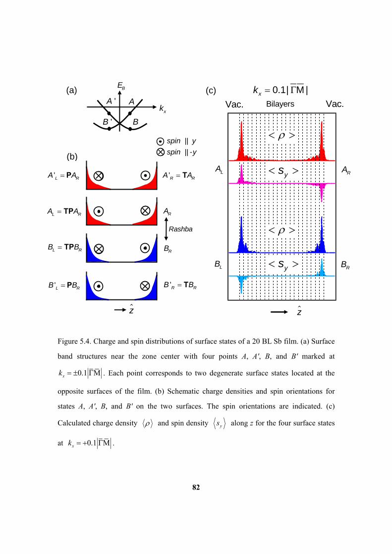
82
Figure 5.4. Charge and spin distributions of surface states of a 20 BL Sb film. (a) Surface
band structures near the zone center with four points A, A', B, and B' marked at
0.1 Mxk . Each point corresponds to two degenerate surface states located at the
opposite surfaces of the film. (b) Schematic charge densities and spin orientations for
states A, A', B, and B' on the two surfaces. The spin orientations are indicated. (c)
Calculated charge density and spin density ys along z for the four surface states
at 0.1 Mxk .
BE
xkA'A
'B B
(a)
LA
LB
z
0.1| M |xk
RB
BilayersVac. Vac.
RA
ys
ys
(c)
(b)
z
Rashba
RA
RB
'R RA AT
'R RB BT
'L RA AP
L RA ATP
L RB BTP
'L RB BP
||
|| -
spin y
spin y

83
Figure 5.5. Calculated plane-averaged electronic charge densities in a 20 BL Sb film for
(a) state AR and (b) state BR. The central plane of the slab is marked by a triangle. (c,d)
Corresponding results computed without spin-orbit coupling.
(a)
(b)
(c)
(d)
1 20
Vac. Bilayers Vac.| M |xk
0.0
0.20.40.60.81.0
0.0
0.20.40.60.81.0
0.00.20.40.60.81.0
0.20.0
0.40.60.81.0
State AR
State BR
State AR (No Spin)
State BR (No Spin)

84
Figure 5.6. (a) Calculated charge separation function, or the normalized absolute charge
moment, as a function of kx for a 20 BL Sb film. (b) The corresponding spin separation
function, or the normalized spin moment, along y.
1.00.50.0
| M |xk
Spi
n S
epar
atio
n C
harg
e S
epar
atio
n 1.0
0.5
0.0
1.0
1.0
0.0
(a)
(b)
Upper State (A) Lower State (B)
Upper State (A) Lower State (B)

85
Figure 5.7. (a) Calculated band structure for a 20 BL Sb film. Ten states at the zone
boundary are indicated by circles. (b) The corresponding charge density distributions in
the film for the ten states. The midpoint of the film is indicated by a triangle.
(b) BilayersVac. Vac.
1 20
(a)
Bin
din
g E
nerg
y (e
V)
M
FE
0.5
0.5
1.0
1.5
Cha
rge
Den
sity

86
Figure 5.8. ARPES mapping of a 20 BL Sb film grown on the Bi-terminated
Si(111)- 3 3 30R surface.
M
1Åk
FE
0.5
1.0
1.50.0 0.5 1.00.5
B
indi
ng E
nerg
y (e
V)
VB
CB

87
Figure 5.9. Calculated band structure of a freestanding 4-BL Sb film. The green band
bordered by dashed lines indicates a positive band gap, within which there is a single
crossing along M by the spin-polarized surface states.
0.0
1.0
1.0
M MK
k
( )E eV

88
Figure 5.10. (a) Band structure of Sb(111) films of various thicknesses. The shaded areas
indicate projected bulk band regions. (b) Calculated energy gap E and (c) logarithmic
gap ln(E) at as a function of film thickness. (d) Plane-averaged charge density of the
lower surface state at as a function of distance from the surface for a thick film. The
vertical dashed lines indicate the bilayers. (e) Same for a 4-BL film.
# BLVac
Cha
rge
De
nsity
(ar
b. u
nits
)
# BLVac Vac
(d)
(e)
(b)
ln(Δ
E/e
V)
Thickness (BL)
(c)
2 4 6 8 10
0.060.08
0.040.02
2
4
6
8
(a)
Ene
rgy
(eV
)
1Åxk
0.0
0.5
0.5
1.0
0.0
0.5
0.5
1.0
0.5 0.0 0.5 0.5 0.0 0.5
MM MM
0.0
0.5
0.5
1.0
0.0
0.5
0.5
1.0
3 BL 4 BL
5 BL 6 BL
2 BL1 BL
10 BL8 BL

89
Figure 5.11. (a) ARPES map for a 4-BL Sb film taken along the M direction. (b)
Calculated band structure of a 4-BL freestanding Sb film. (c) ARPES map for a 20-BL
film. (d) Calculated band structure of a 20-BL freestanding Sb film. (e) Close-up view of
the experimental surface band structure of a 4-BL film. The contrast has been enhanced
by taking the second derivative along the energy axis. (f) Calculated band structure of a
4-BL film suitably broadened to simulate the data. (g) Same as (f) except that the bottom
face of the film is terminated by H. (h) Close-up view of the experimental surface band
structure of a 20-BL film.
M M
E (
eV)
1Åxk0.0 0.1 0.30.20.1 0.4
M M
0.0
0.5
0.0
0.5
0.0 0.1 0.30.20.1 0.4
(a)
(b)
(c)
(d)
M M
H-terminated 4 BL
Freestanding 4 BL
1Åxk
(e)
0.1
0.2
0.0 0.10.1 0.050.05
0.0
0.1
0.2
0.0
0.1
0.2
0.0
0.0
0.1
0.2
0.3
(f)
(g)
(h)
ARPES 4 BL
ARPES 20 BL

90
Figure 5.12. Calculated band structure of a 6-BL Sb film with different bottom surface
conditions: (a) freestanding, (b) bottom layer of Sb atoms replaced with Sb-Bi averaged
pseudo-atoms to simulate a weak interfacial bonding, and (c) bottom face terminated by
H atoms. Also shown side-by-side for comparison are results of the four-band Rashba
model with different surface biases: (d) V = 0, (e) V = 0.05, and (f) V = 2.0.
E (
eV)
1Åxk
Bottom Layer Sb-Bi
M M
0.0
0.2
0.4
0.1 0.0 0.1
0.0
0.2
0.4
0.0
0.2
0.40.1 0.0 0.1
0.05V
2.0V
0.0V
0.03, 0.6, 0.004m
Freestanding
Bottom Layer H-Terminated
(a)
(b)
(c)
(d)
(f)
(e)

91
Figure 5.13. (a) Band structure along kx of the four-band Rashba model (m = 0.03 and =
0.6) with no tunneling ( = 0) and no surface bias (V = 0). (b) and (c) Normalized spin
polarization and magnitude y and y , respectively, for the lower surface band. (d)-(f)
Corresponding results for = 0.004 and V = 0. (g)-(i) Corresponding results for = 0.004
and V = 2.
0.1 0.0 0.1 0.1 0.0 0.1
E (
eV)
0, 0V 0.004, 0V
1Åxk0.1 0.0 0.1
0.004, 2V
(a)
(b)
(c)
(d)
(e)
(f)
(g)
(h)
(i)
1.0
0.4
0.0
0.2
1.0
0.0
0.0
1.0
0.5y
y

92
Figure 5.14. Calculated band structures for (a) a 4-BL and (b) a 6-BL freestanding film.
Corresponding results based on the four-band Rashba model (m = 0.03, = 0.6, V = 0)
are shown for tunneling matrix element = (c) 0.02 and (d) 0.004.
M M
M M
1Åk
6BL0.0
0.2
0.0
0.4
0.2
4BL
0.40.1 0.0 0.10.1 0.0 0.1
(b)(a)
(c) (d)
Ener
gy (e
V)

93
Figure 5.15. Band structures based on the four-band Rashba model with = 0.6 and
various values for the tunneling matrix element and potential bias: (a) = 0 and V = 0, (b)
= 0.008 and V = 0, (c) = 0 and V = 0.04, and (d) = 0.008 and V = 0.04. The direction
of each arrow indicates the spin orientation and the color (red or blue) of the arrow
indicates the surface (top or bottom) at which the electron is localized.
1Åk
0.0
0.1
0.0
0.1
0.1
0.1
0.1 0.0 0.10.1 0.0 0.1
(b)(a)
(c) (d) En
ergy
(eV)

94
Figure 5.16. Calculated band structure for a 4-BL Sb film terminated by Bi atoms on its
bottom face.
1Åk
Bi-terminated face
0.0
0.2
Quantum-well subbands
Top face
0.2
M M
0.40.1 0.0 0.1
Ener
gy (e
V)
95
6 Topological Thin Films: Bi2Se3 and Bi2Te3
6.1 Introduction
Topological insulators are a new class of materials characterized by a bulk band gap,
a strong spin-orbit coupling, and a conducting surface [1,2]. In these materials, an odd
number of spin-polarized surface states span the bulk gap, giving rise to a net surface spin
current at the Fermi level [3,4,5]. This spin current, protected by bulk symmetry, is of
great interest for applications involving spin information processing [6,7]. While the
topological order is a robust quantity, the topological surface states themselves giving rise
to the spin current are not necessarily robust and can be highly sensitive to the boundary
conditions [8,9]. This is a concern, as actual utilization of these materials requires a stable
structure, and surface passivation, capping, or interface formation is generally required
for device architecture. How this topological invariance manifests itself upon surface
modification is an issue of importance to the basic physics of this class of material and
the actual implementation for application. In this chapter there is a demonstration of a
drastic transformation of the topological surface states in a model system under the
constraint of topological-order invariance. Specifically, the surface states of Bi2Se3 and
Bi2Te3 form a single Dirac cone at the zone center [ 10 , 11 , 12 ]. First-principles
calculations based on a slab geometry show that, upon hydrogen termination of either
face of the slab, the Dirac cone associated with this face is replaced by three Dirac cones
centered at the time-reversal-invariant M points at the zone boundary, yet the
topological order remains the same as evidenced by detailed calculations of the wave
functions. Furthermore, the topological surface states on the two faces of the slab, with or
without hydrogen termination, are quantum-mechanically entangled, and the overall

96
topological order of the system must be analyzed within this context.
We also studied the critical behavior of the TI film near the quantum critical point. It
will be shown in the second part of this chapter that the topological surface states, while
protected by symmetry in the bulk limit, can be missing completely in topological films
even at large film thicknesses. This anomalous behavior occurs near the transition from
topological to nontopological phases when the strength of the SOC is tuned across the
critical point. The result is a substantial dead zone where the material is topological but
without surface states, as demonstrated by first-principles simulations for freestanding
Bi2Se3 films. This dead zone is suppressed in an asymmetric film of Bi2Se3 with one face
terminated by H; the nontopological-to-topological transition is signified by a spatial
transfer of a set of Dirac Fermion states from the H-terminated face to the pristine face of
the film to form topological surface states.
6.2 Reorganization of Dirac cones in topological insulators by
hydrogen termination
An often-invoked argument for the robustness of the surface spin current in
topological insulators is that the spin-polarized surface states have a vanishing back
scattering probability by surface perturbations because of time-reversal symmetry; indeed,
experiments have demonstrated the insensitivity of the surface state Dirac cones to
adsorption or gas exposure [13,14]. More generally, though, the surface spin texture can
be affected by spin-orbit coupling through altered electronic orbital motions upon surface
modification, and it is not necessarily an invariant quantity. Specifically, hydrogen
termination leads to surface passivation by saturation of surface dangling bonds. Both the
orbital and spin degrees of freedom of the surface electrons can be substantially altered,
as demonstrated herein for Bi2Se3 and Bi2Te3. The results suggest interesting possibilities
for optimizing material properties or device performance.

97
The band dispersion relations for 6 QL freestanding Bi2Se3 and Bi2Te3 slabs are
presented as solid curves in Figs. 6.1(a) and 6.1(b), respectively. The shaded areas
represent the projected bulk band regions; these results are in good agreement with
previous calculations where available [15,16]. The dashed horizontal lines indicate the
midgap positions, or the bulk Fermi levels. The fundamental band gaps are 0.35 and 0.16
eV, respectively. In each case near the zone center are two surface bands that span
the gap and cross each other at to form a Dirac cone. The Dirac cone has a
left-handed helical spin texture, and the two surface bands have opposite spin
polarizations. Each point on the surface bands, except the Dirac point, is doubly
degenerate corresponding to the surface states located on the two opposite faces of the
slab, which are related by space inversion and time reversal. The two surface bands are
shown in red and blue color to highlight their different spin orientations. They disperse
into the bulk continuum a short distance away from , where they lose their surface
character and become quantum well states [17]. Each band remains doubly degenerate;
the two surface states associated with the two faces of the slab now fully penetrate the
film and combine to form a spin-degenerate pair of quantum well states [18]. Each
quantum well subband is spin degenerate as required by space inversion symmetry.
Results from calculations for the same slab with the bottom face of the slab
terminated by hydrogen are presented in Figs. 6.1(c) and 6.1(d). While the surface bands
near the zone center remain unchanged, a new Dirac cone emerges at M , and these two
cones are smoothly connected throughout the surface zone. With the newly emerged
Dirac cone, the total number of surface band crossings of the bulk Fermi level between
and M becomes an even number (two or four). This is contrasted by a single
crossing for the case without the hydrogen. As is well established, topological insulators
must have an odd number of such crossings. At first glance, our results would seem to
98
violate the topological order of the system, which is a bulk property and cannot be altered
by hydrogen termination.
This puzzling behavior is clarified by considering slabs with both faces terminated by
hydrogen. The results, shown in Figs. 6.1(e) and 6.1(f), reveal the same surface bands
associated with the Dirac cone at M , while the surface bands associated with the Dirac
cone at are eliminated. The number of Fermi level crossings is again odd. Evidently,
the Dirac cone at M is associated with the hydrogen-terminated face, while the Dirac
cone at is associated with the bare face. For the slab with just one face terminated,
both sets of surface bands appear in the calculation. The counting of the Fermi level
crossing for each face of the slab is still consistent with the topological order. There are
three symmetry-equivalent M points in the first zone, thus, hydrogen-termination
results in a trifurcation of the Dirac cone. Hydrogen-termination also breaks the inversion
symmetry of the system. The spin degeneracy of each quantum well subband is lifted [19],
resulting in a small energy splitting, which diminishes with increasing slab thickness.
This splitting is evident for some of the bands in Figs. 6.1(c) and 6.1(d), but not seen in
the symmetrical cases.
The plane-averaged charge densities of the two surface bands are presented in Figs.
6.2(b) and 6.2(c) for a 12-QL Bi2Se3 slab with its bottom face terminated by hydrogen;
the results are presented for 11 equally spaced points between and M as indicated by
the triangles in Fig. 6.2(a). The vertical dashed lines in Figs. 6.2(b) and 6.2(c) indicate the
QLs. The two surface states, labeled and are degenerate at and pinned at the top
face of the slab. Near 0.1 Mxk , state grazes the bulk valence band edge and
develops a charge density more akin to a bulk state. It then evolves, at larger xk , back

99
into the band gap, and the associated charge density becomes pinned at the bottom face
all the way to M . State shows a similar migration of charge density from the top face
to the bottom face, but the transition occurs in a different range in k space. The directions
of the triangles in Fig. 6.2(b), up- and down-pointing, indicate charge localization near
the top and bottom faces of the slab, respectively.
This migration of charge density for each state can be described quantitatively by the
charge localization function
2
x x xC k k z kD
, (6.1)
where D is the film thickness, and z is the normal coordinate of the slab with its origin at
the midpoint of the slab. This quantity ranges from –1 to +1, corresponding to a charge
distribution fully concentrated at the bottom and top faces, respectively. The results,
presented in Fig. 6.3(a), show a rapid passage around the places where the two states
graze the bulk band edges.
The spin polarization of the two surface states and are characterized by the
expectation values of the spin operators. Presented in Fig. 6.3(b) is yS normalized to
2 . Our calculations yield 0x zS S (x points along M , and z points along the
surface normal). The two states are thus strictly polarized along –y and +y, respectively,
in accordance with the Rashba interaction [20], and the directions of spin polarization are
maintained throughout the charge migration from the top to the bottom faces. These
spin-locked channels allow the two faces of the slab to communicate. The magnitude of
the spin polarization, normalized to 2 , is less than 100% because of the coupling of the
spin and orbital degrees of freedom. It is about 50%~60% near where these states are
associated with the bare top face of the slab, and it increases to almost 80% near M ,

100
where they become surface states associated with the hydrogen-terminated bottom face.
Evidently, hydrogen termination enhances the spin polarization of the surface states by
partly disentangling the spin and orbital degrees of freedom.
The hydrogen-induced reorganization of the Dirac cones, from one cone at to
three cones at M , as well as the formation of the spin-locked (or quantum-mechanically
entangled) channels, can be understood qualitatively using the schematic diagram in Fig.
6.4(a). To first order, surface adsorption shifts the overall crystal potential for the surface
states. With increasingly stronger interaction, the Dirac cone is shifted out of the band
gap (middle panel), and eventually the displaced surface bands can intersect again in the
gap at the zone boundary M point, resulting in a new Dirac cone there (bottom panel).
If the band movement can be adjusted, the system could potentially adopt a configuration
with gapless surface states but no Dirac cones in the bulk gap, as indicated in the middle
panel of Fig. 6.4(a). With just one face of the slab terminated by hydrogen, the surface
states on the two faces must connect via avoided crossings through bulk-like states that
are located just at the bulk band edges, as indicated in Fig. 6.4(b). The quantization of the
bulk states into quantum-well-state pairs in films helps isolate the spin-locked surface
bands from the bulk-derived states.
6.3 Evolution of the band structure upon varying the hydrogen
atom position
If the hydrogen atoms are gradually moved from a large distance away to their final
equilibrium adsorption positions on both faces of a Bi2Se3 slab, the band structure should
evolve smoothly from one configuration to the other. The results for several selected
H-Se bond lengths for symmetric H adsorption on a 6 QL Bi2Se3 slab are shown in Fig.
6.5.

101
When the bond length is large, the band structure of the slab is not affected by the
hydrogen as shown in Fig. 6.5(a). With the hydrogen atoms approaching the surfaces, the
original Dirac point at the zone center moves downwards in energy, and eventually
merges into the valence band region. Band , however, remains pinned within the bulk
band gap because of anticrossing. The portion of the band near begins to graze the
valence band edge, and the portion of the band near the M point, originally grazing the
conduction band edge, now moves down into midgap. Time-reversal symmetry (Kramers
theorem) requires double degeneracy at the M point, and this requirement is satisfied
by state dragging its companion quantum well subband into the band gap to form a
new surface band ' . The pair and ' forms a Dirac cone at M for the
hydrogen-terminated surface.
6.4 Hydrogen-induced bonding states below the p valence bands
In addition to modifying the gapless surface states, hydrogen adsorption gives rise to
new surface states within bulk band gaps. A prominent example is seen in Fig. 6.5 where
two H-induced surface bands, H and H , arise within the s-p gap (the lower s bands
are not shown). This pair shows the usual Rashba splitting and is topologically trivial.
Presented in Fig. 6.6 are the charge distributions of states H and H at for a 12
QL Bi2Se3 slab with its bottom face terminated by H. The charges are strongly localized
near the H-Se bonds. The calculated spin polarizations of these states are nearly 100%.
6.5 Robustness of the first-principles results
The calculations described in the main text were performed using LDA. To test the
robustness of the results, we show in Figs. 6.7(a) and 6.7(b) the calculated dispersion

102
relations for a 6 QL slab of Bi2Se3 with its bottom face terminated by hydrogen using two
different exchange-correlation functionals: LDA and Perdew-Burke-Ernzerhof GGA,
respectively. In each case, the H atom position is optimized energetically. The results are
nearly identical; the main difference is that the Dirac point is at a slightly different energy.
We have also explored the issue of atomic relaxation by allowing the positions of the
surface layer of Bi2Se3 and the H atoms to relax in the LDA calculation. We find that the
Se atom adjacent to each H atom moves outwards by 0.01 Å and the length of the H-Se
bond is elongated by 0.05 Å. These slight atomic movements are not expected to cause
significant changes in the calculated band structure. Indeed, the results, presented in Fig.
6.7(c), are very close to those in Figs. 6.7(a) and 6.7(b). Specifically, the topological
properties of the system remain the same. Thus, our conclusions are independent of the
details of the calculation.
6.6 Bulk band structures and parity eigenvalues of Bi2Se3
with/without SOC
Bi2Se3 has a rhombohedral crystal structure with nine occupied valence bands. There
are eight time-reversal-invariant momenta (TRIMs) in the first Brillouin zone: (0, 0, 0),
Z(0.5, 0.5, 0.5), three equivalent F(0.5, 0.5, 0), and three equivalent L(0.5, 0, 0). We
define in to be the parity eigenvalue of the n-th valence state at the i-th TRIM, where n
= 1-9 and i = 1-8. We also define PdTRIM as the product of the parity eigenvalues of the
nine valence states at each TRIM and Pdband as the product of the parity eigenvalues at
the eight TRIMs for each band. The topological invariant is given by
8 9 8 9
1 1 1 1( 1)
TRIM band
in i ni n i n
Pd Pd . (6.2)
If the total product of the parity eigenvalues is 1 , 1 and the material is topological.

103
Otherwise, it is nontopological. The bulk band structures of Bi2Se3 without and with SOC
are shown in Figs. 6.8(a) and 6.8(b), respectively. The corresponding parity eigenvalues
are listed in Table 6.1. The calculated topological invariant reveals that Bi2Se3 without
SOC is nontopological and vice versa. The crucial differences between the two cases,
with or without SOC, happen at the zone center for the top valence band V1 and the
bottom conduction band C1. The two states exchange their opposite parities across the
transition, resulting in gap inversion.
6.7 Topological phase transition and Dirac fermion transfer in
Bi2Se3 films
Device applications of topological materials must involve thin films for large-scale
integration; how thin the films can be without losing their desirable characters is a key
question. This issue is tied to the strength of the SOC. Changing the effective SOC
strength can be realized experimentally by alloy substitution with elements in the same
columns in the period table, such as substituting Sb for Bi and/or S for Se in Bi2Se3
[ 21 , 22 ]. The phenomenon of missing topological surface states near the
topological-to-nontopological transition is a much more severe issue than a tunneling gap
in the surface states that can open up as a result of the interaction between the two faces
of the film. The tunneling gap does not preclude spin-polarized surface states and can be
avoided by Fermi level tuning. Without surface states altogether, the system is insulating
and useless for transport applications.
For bulk topological insulators with space-inversion symmetry, such as Bi2Se3, the
Z2 topological order is determined by the parity product of the valence states at
time-reversal-invariant momenta (TRIMs) in the first Brillouin zone [23]. Calculations of
the band structure at various levels of SOC strength (Fig. 6.9(b)) ranging from 0 to 100%
confirm that Bi2Se3 is naturally topological, but becomes nontopological as the SOC is

104
reduced to below 31.2%. At this quantum critical point (QCP), the conduction and
valence band edges cross each other at , resulting in a parity exchange and a gap
reversal, which causes the system to undergo a topological-to-nontopological transition.
The calculated fundamental gap (Fig. 6.9(c)) crosses zero at the QCP, which separates the
nontopological phase ( = 0) from the topological phases ( = 1).
Surface properties are not available from bulk calculations. Instead, we perform a
slab calculation for a Bi2Se3 freestanding film of a thickness of 6 quintuple layers (QLs).
Prior theoretical and experimental work has shown that the surface states at this thickness
are essentially in the bulk limit with a negligible tunneling gap [24]. The calculated band
dispersion relations with different SOCs are shown in Figs. 6.10(a)-6.10(d). The shaded
areas indicate the projected bulk band regions. At 100% SOC, the system shows a pair of
surface states forming a Dirac cone at and bridging the bulk gap. At 0% and 20%
SOCs, the system is an ordinary insulator with no surface states. The case of 40% SOC is
peculiar. The system is beyond the QCP and should be topological, but all of the states
correspond to quantum well states. The apparent gap between the lowest conduction band
and the highest valence band is induced by the tunneling effect between the topological
surface states on the opposite surface. The coupling of surface states is roughly one half
of the size of the apparent tunneling gap. In other words, without the tunneling effect this
gap should vanish and a gapless Dirac cone should form within the bulk band gap. The
topological surface states do not emerge until SOC becomes greater than 48%. Thus,
there is a wide dead zone between the QCP of 31.2% and the onset point (OSP) of
surface states at 48%. The results are summarized in Fig. 6.10(e), where the absolute bulk
gap is indicated by hatching, and the apparent gap between the lowest conduction band
and the highest valence band is indicated by a curve. This curve crosses the QCP with an
apparent gap of 0.18 eV, where the bulk gap vanishes; it crosses the OSP where the
apparent gap equals the bulk gap of 0.11 eV. Beyond the OSP, the apparent gap becomes

105
smaller than the bulk gap and the relevant states transform from quantum well states into
surface states. The apparent gap does not vanish until SOC reaches about 80%, the
saturation point (SP).
Calculations for a 10-QL Bi2Se3 film reveal a similar pattern (Fig. 6.10(e)). The dead
zone, ranging from QCP = 31.2% to OSP = 42%, is smaller but still quite significant. The
SP is reduced to about 70%. For the -QL case (Fig. 6.10(e)), or the bulk limit, there are
no surface states in the bulk gap below the QCP, and the system is an ordinary insulator.
The topological surface states emerge beyond the QCP and form a Dirac cone at with
zero apparent gap.
A crude argument for the dead zone is a tunneling gap so large that the surface states
are pushed out of the bulk gap. Rigorously speaking, this argument is incorrect because it
assumes that surface states exist to begin with, an assumption not supported by the results.
One way to suppress the tunneling gap effect is to make the film asymmetric, thus
removing the degeneracy coupling of the surface states associated with the two faces of
the film [25,26]. We consider here a 6-QL Bi2Se3 film terminated by hydrogen on the top
face; energy-minimization calculations show a hydrogen atom on top of each surface
selenium atom at a H-Se bond length of 1.46 Å. The calculated band dispersion relations
(Figs. 6.11(a)) with the SOC set to 0, in comparison with the case without H (Fig.
6.10(a)), reveal a H-induced surface band within the bulk gap. The associated charge
density is localized near the H-terminated face except at the point, where the surface
band grazes the tip of the valence band region to yield a diffuse wave function in the film.
The pristine face at the bottom of the film has no topological surface states in agreement
with the results for the freestanding film (Fig. 6.10(a)).
With the SOC turned on to 20% (Fig. 6.11(b)), the H surface band becomes spin

106
split due to the Rashba interaction and develops two chiral Dirac cones, one at and
the other at M . The appearance of a pair of Dirac cones is in agreement with the chiral
Fermion doubling rule [27]. Both Dirac cones are still localized near the H-terminated
face. The system remains topologically trivial based on the usual rule of counting Fermi
level crossings for each face. With the SOC raised to 40% (beyond the QCP), the material
becomes topological, but the band structure (Fig. 6.11(c)) appears similar to the 20% case
albeit with a larger spin splitting. However, expanded views of the band structure near
(Figs. 6.11(e) and 6.11(f)) show that the Dirac cone does not span the bulk gap at SOC =
20% but does so at 40%. Bulk gap spanning is a necessary, but not a sufficient, condition
for "partner switching" and a nontrivial surface topological order [28].
The calculated three-dimensional charge distributions of the H-terminated 6-QL
Bi2Se3 film at various levels of SOC reveal that the Dirac surface states at M remain
localized at the H-terminated (top) face throughout the entire range of SOC variation (Fig.
6.12(b)). The main change in the dispersion relation (Fig. 6.11(a-d)) is the magnitude of
the spin-orbit splitting. By contrast, the Dirac Fermion states near (Fig. 6.12(a))
undergo a charge transfer from the H-terminated (top) face to the pristine (bottom) face
with the SOC increasing through the QCP. For this calculation, we pick the upper surface
band at a point slightly offset from (at 0.025 1Å or ~3% ΓM ) to avoid the
degeneracy with the bulk valence band edge at SOC below the QCP. Thus, with the SOC
below the QCP, both Dirac cones at and M are associated with the H-terminated
surface, and the two surface bands remain within the bulk gap. With the SOC crossing the
QCP, the Dirac cone Fermions at transfer to the pristine face, and simultaneously the
surface bands touch both the conduction and valence band edges to bridge the bulk gap.
Each Dirac cone yields just one Fermi level crossing per face of the film, and the system

107
is topological based on the counting of Fermi level crossings.
The spatial transfer of the Dirac cone Fermions near can be quantified by the
charge moment
| |SS SSz
PD
(6.3)
where D is the film thickness, is the normalized charge density operator and z = 0 is at
the midpoint of the Bi2Se3 film. Its absolute value ranges from 0 (symmetric bulk states)
to 0.5 (tightly bound surface states) and its sign indicates the charge bias (+ toward the
H-terminated face, and – toward the pristine face). The calculated results (Fig. 6.12(c))
show a spatial transfer of the Dirac cone states at across the QCP. With H-termination,
there is an ambiguity about the "midpoint" of the film, and this accounts for the slight
offset of the zero crossing of the curve.
6.8 Band structures of a 6-QL Bi2Se3 film with the top face
terminated by F or Cl
We have computed the effects of F and Cl termination of a 6-QL Bi2Se3 film to
simulate the effects of interfacial bonding to highly electronegative surfaces. The results
for the two cases are very similar. Without SOC, there is a surface band induced by the
adsorbate (Fig. 6.13). The band shapes are similar to the case of H-termination, but the
surface band sticks to the bottom point of the conduction band region instead of the top
point of the valence band region. The atomic orbitals involved in the surface states are the
1s orbital of H, the 2p orbital of F, and the 3p orbital of Cl. The s and p orbitals have
different parities, and the corresponding surface states must connect to either the
conduction or valence band edge with a compatible parity.

108
6.9 Conclusion
In this chapter we demonstrates that the surface states of topological insulators as
well as their associated spin structure and degree of spin polarization can be substantially
modified by surface and/or interface engineering. The reconfigured surface states still
satisfy the requirements of topological order and time-reversal symmetry. Robustness of
the surface states against surface perturbation because of a vanishing back scattering
probability does not prevent these states from transforming into drastically different
configurations. These conclusions are independent of the details of the model as
demonstrated by additional calculations using the GGA approximation or allowing
surface atomic layer relaxation. Our findings suggest opportunities for optimization of the
spin current and spin texture. For thin films in the ballistic transport regime, the spin
currents of the two opposite faces of the film could be connected with locked spin
directions through bulk-like states without going through the side faces. This connection
is a unique feature of topological insulators.
Moreover, the phenomenon of the dead zone, where topological insulator films
exhibit no topological surface states and behave like band insulators, sets a lower limit on
the film thickness suitable for device applications. This limiting thickness can be quite
large in "marginal" topological insulators with a relatively weak SOC. This dead zone
effect can be suppressed in an asymmetric film configuration, which can be readily
realized in experiments or actual device configurations by growing the film on a substrate
with a strong interfacial bonding to break the degeneracy coupling underlying the
tunneling effect. The restoration of the topological surface states on the pristine face in
the dead zone is via spatial transfer of Dirac Fermion states from the other face; thus, the
evolution of the system remains analytically continuous.

109
References:
[1] M. Z. Hasan and C. L. Kane, Rev. Mod. Phys. 82, 3045 (2010).
[2] X. L. Qi and S. C. Zhang, Rev. Mod. Phys. 83, 1057 (2011).
[3] D. Hsieh et al., Nature 452, 970 (2008).
[4] L. Fu and C. L. Kane, Phys. Rev. B 76, 045302 (2007).
[5] R. Roy, Phys. Rev. B 79, 195322 (2009).
[6] I. Garate and M. Franz, Phys. Rev. Lett. 104, 146802 (2010).
[7] L. Fu and C. L. Kane, Phys. Rev. Lett. 100, 096407 (2008).
[8] Y. L. Chen et al., Science 329, 659 (2010).
[9] O. V. Yazyev, J. E. Moore and S. G. Louie, Phys. Rev. Lett. 105, 266806 (2010).
[10] Y. Xia et al., Nat Phys 5, 398 (2009).
[11] Y. L. Chen et al., Science 325, 178 (2009).
[12] Y. Zhang et al., Nat Phys 6, 584 (2010).
[13] H. M. Benia, C. Lin, K. Kern and C. R. Ast, arXiv:1105.2664v1 (2011)
[14] Z.-H. Pan, D. R. Gardner, S. Chu, Y. S. Lee and T. Valla, arXiv:1104.0966v1 (2011)
[15] Z. Wei et al., New J. Phys. 12, 065013 (2010).
[16] H. Zhang et al., Nat Phys 5, 438 (2009).
[17] T. C. Chiang, Surf. Sci. Rep. 39, 181 (2000).

110
[18] G. Bian, T. Miller and T.-C. Chiang, Phys. Rev. Lett. 107, 036802 (2011)
[19] J. H. Dil et al., Phys. Rev. Lett. 101, 266802 (2008).
[20] Y. A. Bychkov and J. Rashba, Phys. C: Solid State Phys. 17, 6039 (1984).
[21] S. Xu, et al., Science 332, 560 (2011).
[22] T. Sato, et al., Nat. Phys. 7, 840 (2011).
[23] Z. Wei, et al., New J. Phys. 12, 065013 (2010).
[24] G. Bian, et al., Phys. Rev. Lett. 108, 176401 (2012).
[25] G. Bian, et al., Phys. Rev. B 84, 235414 (2011).
[26] X. Wang, et al., Phys. Rev. Lett. 108, 096404 (2012).
[27] N. B. Nielsen and M. A. Ninomiya, Phys. Lett. B 105, 219 (1981).
[28] D. Hsieh, et al., New J. Phys. 12, 125001 (2010).

111
Figures and tables:
0%
SOC
V9 V8 V7 V6 V5 V4 V3 V2 V1 PdTRIM C1
+1 -1 -1 -1 +1 +1 -1 -1 -1 +1 +1
L (3) -1 -1 -1 -1 -1 -1 +1 +1 +1 +1 +1
F (3) -1 +1 -1 -1 -1 +1 +1 -1 -1 +1 +1
Z -1 -1 +1 -1 +1 +1 -1 -1 -1 +1 +1
Pdband -1 -1 -1 +1 +1 -1 +1 -1 -1 +1 +1
100%
SOC
V9 V8 V7 V6 V5 V4 V3 V2 V1 PdTRIM C1
-1 +1 -1 +1 -1 +1 -1 -1 +1 -1 -1
L (3) -1 -1 +1 -1 -1 -1 -1 +1 +1 +1 +1
F (3) -1 +1 -1 -1 +1 -1 -1 +1 -1 +1 +1
Z -1 -1 +1 -1 +1 +1 -1 -1 -1 +1 +1
Pdband +1 +1 +1 -1 +1 +1 +1 +1 +1 -1 -1
Table 6.1. Parity eigenvalues at the eight TRIMs of the nine valence bands and the lowest
conduction band of Bi2Se3 calculated without/with spin-orbit coupling.

112
Figure 6.1. (a and b) Calculated dispersion relations (solid curves) for 6 QL slabs of
Bi2Se3 and Bi2Te3, respectively. The shaded areas are projected bulk band regions. The
horizontal dashed lines indicate the bulk Fermi levels. The red and blue curves represent
surface states and their continuations into the bulk regions. (c and d) Results after the
bottom faces of the slabs are terminated by hydrogen. (e and f) Results after both faces
are terminated by hydrogen.
Ene
rgy
(eV
)
0.5
0.0
1.0
MMK M MK
0.5
0.5
1.0
0.5
0.0
0.5
0.5
1.0
0.0

113
Figure 6.2. (a) Surface bands, and , of a 12 QL slab of Bi2Se3 with its bottom face
terminated by hydrogen. (b and c) Plane-averaged electronic charge densities for the two
states.
QLs QLsTop TopBottom Bottom
(a)
(b) (c)
Mxk
0.2
0.2
0.0
0.4
Cha
rge
Den
sity
(a
rb.
un
its)
Ene
rgy
(eV
)
| M |
xk
0.0
0.1
0.2
0.3
0.4
0.5
0.6
0.7
0.8
0.9
1.0

114
Cha
rge
Loca
lizat
ion
Figure 6.3. (a) Charge localization as a function of kx (along M ) for the two states
and in a 12 QL slab of Bi2Se3 with its bottom face terminated by hydrogen. It equals +1
and –1 for charge fully localized at the top and bottom faces of the slab, respectively. (b)
Calculated spin polarization 2 yS .
1.0
0.0
1.0
0.0
1.0
1.0
0.5
0.5
0.5
0.5
1.00.60.0
| M |xk0.40.2 0.8
2 yS
(a)
(b)

115
Figure 6.4. (a) Displacement of Dirac cones in the vertical direction relative to the bulk
conduction band (CB) and valence band (VB) as the surface potential changes. (b) The
top two diagrams correspond to semi-infinite substrates, one without and the other with
hydrogen termination; the Dirac cones are located at and M , respectively. For a
finite slab with just the bottom face terminated by hydrogen, the Dirac cones associated
with the two faces must connect by analytic continuation (or anti-crossing), resulting in
spin-locked channels as shown in the bottom diagram.
H-terminated
V B V B
C B C B
M
Bare surface
Semi- substrate
Slab with one face
terminated by H
V B
C B
Spin-locked
channels
M M
V B
V B
C B
C B
V B
(a) (b)
C B

116
Figure 6.5. Evolution of band structure as hydrogen adatoms approach both faces of a 6
QL Bi2Se3 slab. The H-Se bond length is (a) , (b) 3.00, (c) 1.91, and (d) 1.46 Å
(equilibrium bond length).
Ene
rgy
(eV
)

117
Figure 6.6. (a) Hydrogen-termination-induced bands H and H for a 12 QL Bi2Se3
slab with its bottom face terminated by H. (b) Charge distributions of states H and
H at the zone center .
Ene
rgy
(eV
)

118
Figure 6.7. Calculated dispersion relations for a 6 QL slab of Bi2Se3 with its bottom face
terminated by hydrogen. Only the position of the H atom is optimized using (a) LDA and
(b) GGA for the exchange-correlation functional. (c) The surface Se atomic layer of
Bi2Se3 and the H atoms are relaxed using LDA.
0.2
0.0
0.2
0.4
0.4
0.2
0.0
0.2
0.4
0.4
Ene
rgy
(eV
)
kx
(a)
0.2
0.0
0.2
0.4
0.4
(b)
(c)
M

119
Ener
gy (e
V)
Figure 6.8. Bulk band structure of Bi2Se3 without/with SOC.
(a)
2.0
-2.0
0.0
-4.0
-6.0
2.0
-2.0
0.0
-4.0
-6.0
F L Z
0% SOC
100% SOC
C1
V1V2
V3V4V5V6V7V8
V9
C1
V1V2
V3V4V5V6V7V8
V9
(b)

120
20%
31.2%
50%
100%
Figure 6.9. (a) Bulk and surface Brillouin zones of Bi2Se3 with the special points
indicated. (b) Calculated bulk band structure of Bi2Se3 at various strengths of the SOC. (c)
The bulk band gap at as function of SOC. The gap is positive when the state with odd
parity is above the state with even parity.
Non- topological Topological
(b)
SOC (%)
0.4
0.0
0.2
0 10080604020
0.6
= 0 = 1
(c)
F L Z
0.51.0
0.0-0.5-1.0
F L Z
F
L
Z
KM
K
Gap
(eV)
Ener
gy (e
V)
(a)0.51.0
0.0-0.5-1.0
0.51.0
0.0-0.5-1.0
0.51.0
0.0-0.5-1.0
0.51.0
0.0-0.5-1.0
0%

121
Figure 6.10. (a)-(d) Band structures of a freestanding 6-QL Bi2Se3 film with the SOC at
0%, 20%, 40% and 100%, respectively. (e) The apparent gap at as a function of SOC
for 6-, 10-, and -QL films. The hatched area indicates the absolute bulk gap.
0.5
0.0
-0.5
0.5
0.0
-0.5
M M M MEn
ergy
(eV)
0%
100%
20%
40%
(b)
(c)
(a)
(d)
Gap
(eV)
SOC (%)
0.10
0.00
0.05
0
0.15
0.20
0.25
10080604020
6 - QL
10 - QL
- QL
QCP
6OSP
6SP
(e)
10OSP
10SP

122
Figure 6.11. (a)-(d) Band structures of a 6-QL Bi2Se3 film with the top face terminated by
H with the SOC at 0%, 20%, 40% and 100%, respectively. The shaded regions indicate
projected bulk band regions. (e) and (f) Close-up views of the band structures near
with the SOC at 20% and 40%, respectively.
0.10
0.00
0.05
-0.05
-0.10-0.05
Ener
gy (e
V)
0 0.05 -0.05 0 0.05 1Åk
20% - H 40% - H(e) (f)
Ener
gy (e
V)
0.5
0.0
-0.5
0.5
0.0
-0.5
0% - H
100% - H
20% - H
40% - H
M M M M(a) (b)
(c) (d)

123
Figure 6.12. (a) and (b) Three-dimensional charge distributions for the upper surface state
near and the surface state at M , respectively, at various SOC strengths. (c) The
corresponding charge moments P for the two cases.
(c)
M
0 20 40 60 80 100
0.0
0.2
0.4
-0.2
-0.4
SOC (%)
P
(a) 100%40%20%0%SOC
60% 80%
M1a a2
c
HSe
Bi(b)

124
Figure 6.13. Band structures of a 6-QL Bi2Se3 film with its top face terminated by F (right
panel) or Cl (left panel). The shaded areas indicate the projected bulk band regions. The
spin-orbit coupling is turned off
-0.5
0.0
0.5
MMEn
ergy
(eV)
Cl - termination F - termination

125
7 Epitaxial Bi Films on Si(111): Surface-Mediated
Metastability
7.1 Introduction
Semi-metallic Bi has attracted intense interest because of its unique combination
of physical properties including a strong spin-orbit coupling, a large Fermi wavelength,
and a small Fermi surface with Dirac-like band features that are tunable by doping or
alloying [1,2,3,4,5]. These attributes make Bi a promising candidate for electronic and
spintronic applications [6]. In this chapter, we report the observation of a metastable
pseudocubic (PC) phase of Bi films made by annealing initially disordered films of
thicknesses 20 to ~100 Å deposited on Si(111)-(77) at low temperatures. The
metastability of the PC phase is demonstrated by the transformation, upon annealing to
higher temperatures, to the stable rhombohedral (RH) bulk phase. The two phases are
easily distinguished by angle-resolved photoemission as they exhibit different surface
states and quantum-well subbands [7]. While the electronic structure of the RH phase has
been well characterized in prior studies [8,9,10], the present work provides the first
detailed experimental mapping of the surface states and the quantum-well subbands in
the metastable PC phase. It is interesting to note that the two phases have nearly the same
atomic volume, but the measured band topologies are very different. Specifically, the
curvatures of the subbands at the zone center have opposite signs. The RH phase
shows a Dirac-like subband around M along K M K [11,12], which is absent in the
PC phase. A bundle of surface states in the RH phase below the Fermi level is replaced
by a concave surface band in the PC phase that moves slightly upward and pokes through
the Fermi level with increasing film thicknesses. These observations are in generally

126
good accord with first-principles slab calculations.
The metastable behavior is observed over a film thickness range from 20 to ~100 Å.
Below 20 Å, the film's structure after annealing is always the PC phase; above ~100 Å,
the only stable phase is RH. For comparison, previous scanning tunneling microscopy
(STM) work on Bi films reported a surface structure identified as that of the PC phase for
film thicknesses equal to or less than 4 bilayers (BL) (13 Å; see below for an explanation
of the bilayer); thicker films showed a surface structure consistent with the RH phase
[13,14]. The critical thickness of 4 BL was attributed to a crossover of the relative
importance of the surface and bulk energies of the films, with the PC phase having a
lower surface energy. Evidently, the previous STM study did not look specifically for
metastable structures, and our study shows that the critical thickness is 6 BL instead. At
the upper thickness limit of metastability (~100 Å), the surface bilayer constitutes just
~4% of the system; this has strong implications regarding the energetics of the
metastable-to-stable phase transformation.
7.2 Sample preparation and computational methods
In our experiment, an n-type Si(111) wafer (Sb-doped with a resistivity ~0.01 cm )
was used as the substrate. It was cleaned by direct current heating to yield a (77)
reconstructed surface. Bi was deposited onto the substrate maintained at 60 K. The
amount of deposition was measured by a quartz thickness monitor. The film after
deposition was disordered based on in-situ electron diffraction. Annealing was performed
by passing a current through the sample.
For comparison with the experimental results, we performed first-principles slab
calculations of the electronic structure of the films using HGH-type pseudopotentials and
a plane-wave basis set [15]; the main program employed was developed by the ABINIT

127
group [16,17]. Appropriate surface relaxation parameters were included in the structural
model [18]. Spin-orbit coupling, which is crucial for the description of the electronic
structures of heavy elements such as Bi, was included in the calculation.
7.3 Metastability of epitaxial Bi films
Figure 7.1 shows model drawings of the PC and RH structures [8,18]; each can be
described in terms of a stack of BLs, where each BL contains two closely spaced atomic
layers. The RH films are oriented along [111]. Currently there are two proposed
structural models for the PC phase: one is a black-phosphorus-like structure and the other
is a slightly expanded (by ~1%) bulk-like structure oriented along [110]. The differences
between the two models are fairly minor [19], but the latter matches our data slightly
better and is shown in Fig. 7.1. Within this model, the PC and RH films have similar bulk
structures but different crystallographic orientations. The atomic density of 1 BL is 1.12
1015 atoms/cm2 for the RH phase and 9.27 1014 atoms/cm2 for the PC phase; thus, 1
BL of RH is equivalent to 1.21 BL of PC. The nominal thickness of each BL is 3.93 Å for
the RH phase and 3.28 Å for the PC phase. The PC to RH transformation thus involves a
rather unusual rearrangement of the incommensurate layer structures. In the following,
we will refer to the film thickness in terms of either the PC BL or the RH BL, where
appropriate. The surface Brillouin zones for the two phases are shown in Fig. 7.1; the
direction mapped by the photoemission measurements corresponds to the M and K
directions of the PC and RH phases, respectively.
Figure 7.2(a) shows photoemission results for a 6 BL PC film obtained by
annealing to 350 K; this thickness is the upper limit of stability for PC. Figure 7.2(b)
shows the same data differentiated twice along the energy axis. This differentiation
effectively removes a background and enhances the contrast for a better visualization of
the band dispersions. Figure 7.2(c) is the results of our first-principles slab calculation for

128
comparison. Overall, there is a good agreement between the present calculation, a
previous calculation [18], and the experiment. Experimentally, the top subband (marked
by small circles) has a concave shape near and nearly grazes the Fermi level. A
comparison of the calculated slab band structure to a calculated projected bulk band
structure reveals that this band has a surface character near (see below for further
evidence). While this band is fully occupied based on the experiment, the calculation puts
it slightly higher, resulting in a hole pocket at . The experiment and calculation agree
that the next few subbands below are nearly flat near , and the ones further below
become convex.
Figure 7.3(a) presents the photoemission results from a film of thickness
equivalent to 20 BL in the PC phase or 17 BL in the RH phase. After deposition, the film
was annealed to 280 K and cooled back to 60 K; its structure is PC. The second
derivative of the data is present in Fig. 7.3(b). The results are similar to those seen in Fig.
7.2, but with more densely packed quantum well subbands as expected. The top subband
near , indicated by circles, is distinctly separated from the others because of its surface
character. Compared to the 6 BL case, it has moved slightly upward to create a small hole
pocket at . These features are generally consistent with the theoretical results shown in
Fig. 7.3(c). The calculation shows pairs of subbands near , which arise from a pair of
closely spaced bulk bands of Bi along the direction [12]. The energy difference
in each pair is too small to be resolved experimentally; thus, each pair appears in the
experiment as a single broadened subband.
Figure 7.4 presents theoretical evidence for the surface and bulk characters of the
various states. The upper panel shows a detailed view of the band structure near the

129
Fermi level for a 20 BL Bi film in the PC phase; several states A-E are marked. The
corresponding plane-averaged charge densities for these states are shown in the lower
panel. Evidently, states A and B are derived from bulk states, while states C-E are surface
states as they decay away from the surfaces. The decay lengths of the surface states are
quite long; at small film thicknesses, the charge distributions localized near the two
surfaces join, and a charge density plot alone is insufficient to make a positive
identification of the surface character.
The photoemission spectra from the same film change dramatically after
annealing to 350 K, as seen in Fig. 7.3(d) and its second derivative in Fig. 7.3(e). The set
of convex quantum well subbands near at binding energies 1-2 eV for the PC phase
have disappeared. Instead, one observes a bundle of closely packed concave bands with
complex structures near . For comparison, Fig. 7.3(f) presents the results of our slab
calculations for the RH structure, with the surface states indicated by small circles. The
similarities between the experiment and theory are apparent, thus confirming the RH
structure of the film. Our results also agree with a previous photoemission mapping of
the bands for the RH phase [8,9]. The calculated results in Fig. 7.3(f) show a bunch of
surface states at low binding energies near . This is seen in photoemission as an
intense peak at ~0.4 eV.
Of special interest are the bands near M , where there is an excellent agreement
between the calculation and experiment. Near the Fermi level, a small gap, marked by D,
separates a -shaped lower band and a V-shaped upper band. These dispersion relations
are nearly-Dirac-like along K M K . In the bulk limit, the region under the
-shaped band is completely filled with bulk states. Quantum size effects lead to
discretization of the bulk band continuum and bring about the Dirac-like dispersion. The

130
present work suggests that quantum size effects could be an additional mechanism for
modifying the band structure and realizing Dirac physics in low-dimensional systems.
Experimentation with various film thicknesses has established the PC-RH
metastability regime to range from 20 to ~100 Å (6 BL PC phase to ~27 BL RH phase).
The transformation from PC to RH is illustrated by the results presented in Fig. 7.5. The
top row displays photoemission data from a 14 BL (referred to the RH phase) Bi film
recorded at various sample temperatures while the sample temperature was raised slowly.
The corresponding second derivatives are shown in the bottom row. The spectra taken
before annealing are featureless because of structural disorder. Features associated with
the PC phase emerge around 250 K and become fully developed at ~300 K. Further
annealing to 315-335 K results in a mixture of the PC and RH phases, as one can detect
the characteristic subband dispersions of both phases in the data. Annealing to 350 K
fully converts the film to the RH phase. Annealing to even higher temperatures leads to
broadening and fading of the subbands, which can be attributed to thermal roughening of
the film.
An inspection of the data in Fig. 7.5 reveals that the quantum-well subbands for
the PC phase remain at the same energy positions throughout the gradual transition to the
RH phase. If the phase transformation begins at the surface or interface of the film and
propagates thickness-wise, one would expect the quantum-well subband structure of the
PC phase to evolve in accordance with a gradual reduction in film thickness. This is
clearly not the case based on the experiment. We conclude that the transformation mainly
involves the formation of lateral domains that expand laterally as the annealing
progresses.
Previous studies have proposed that the PC structure is stable at lower thicknesses
because it has a lower surface energy (but a higher bulk energy) [13,14]. As the film

131
thickness increases, the surface contribution diminishes relative to the bulk contribution,
and the total energy of PC becomes higher than that of RH at thicknesses greater than 6
BL (or 4 BL based on the previous STM study). But why does the PC phase persist as a
metastable phase to a rather large film thickness of ~100 Å? A physical picture is as
follows. As an initially disordered film is annealed, it is likely that the atoms at the
surface become mobile first because of the reduced coordination. The surface atoms tend
to adopt the PC structure locally for its lower energy, and the ordering then propagates
throughout the film resulting in a metastable PC film. Thus, the metastable phase
formation is likely a kinetic effect associated with surface nucleation. Annealing to higher
temperatures causes the system to make a transformation to the stable phase. The
annealing temperature needed for this transformation, ~350 K, corresponds to just 30
meV, a very small thermal energy. This suggests that the barrier for the phase
transformation is very low. Furthermore, the metastable phase persists to a large thickness
(~100 Å) at which the surface bilayer constitutes just ~4% of the film. This suggests that
the difference in bulk energies between the two phases is very small; otherwise thermal
fluctuations could readily bring the system over the barrier and down a steep energy slope,
thus severely restricting the range of metastability. The near degeneracy of the bulk
energy is consistent with the observation that the two phases have nearly the same bulk
structure, the main difference being a slight expansion by ~1% of the PC phase. It is
interesting to note a somewhat analogous behavior of another group V element, P, which
exhibits a PC-RH transition upon compression under pressure [20,21].
7.4 Conclusion
In this chapter, the study based on photoemission demonstrates the existence of a
metastable PC phase and a stable RH phase of Bi films over a wide range of film
thickness from 20 to ~100 Å. Below 20 Å, PC is the only ordered phase observed; above

132
~100 Å, RH is the only one. The quantum well subband structures for the two phases
have very different topologies, which make a positive identification of the phases
straightforward. This is a much more robust identification of the internal film structure
than STM or electron diffraction observation of the (near) surface atomic geometry. The
complex electronic structures of the two phases as determined by photoemission are
confirmed by first-principles slab calculations. Among the many interesting electronic
features, the PC phase has a surface band at that grazes the Fermi level, while the RH
phase has a Dirac-like subband at M along K M K . The PC-RH metastability
range of 20 to ~100 Å is unusually wide, but it can be understood in terms of a near
degeneracy of the bulk energies of the two phases and a surface-nucleation process that
facilitates the formation of the metastable phase. Subbands in thin films can be tuned by
changing the film thickness; together with metastability, the results suggest opportunities
for fine tuning the electronic structure of Bi films, a system of interest for spintronic
applications.
References:
[1] Y. M. Koroteev et al., Phys. Rev. Lett. 93, 046403 (2004).
[2] C. R. Ast and H. Höchst, Phys. Rev. Lett. 87, 177602 (2001).
[3] C. R. Ast and H. Höchst, Phys. Rev. B 67, 113102 (2003).
[4] J. Fan and J. Eom, Appl. Phys. Lett. 92,142101 (2008).
[5] D. Hsieh et al., Nature 452, 970 (2008).
[6] I. Žutić, J. Fabian, and S. Das Sarma, Rev. Mod. Phys. 76, 323 (2004).
[7] T.-C. Chiang, Surf. Sci. Rep. 39, 181 (2000).

133
[8] T. Hirahara et al., Phys. Rev. Lett. 97, 146803 (2006).
[9] T. Hirahara et al., Phys. Rev. B 76, 153305 (2007).
[10] T. Hirahara et al., Phys. Rev. B 75, 035422 (2007).
[11] P. A. Wolff, J. Phys. Chem. Solids 25, 1057 (1964).
[12] Y. Liu and R. E. Allen, Phys. Rev. B 52, 1566 (1995).
[13] T. Nagao et al. Phys. Rev. Lett. 93 105501 (2004).
[14] S. Yaginuma et al. J. phys. Soc. Jpn. 77, 014701 (2008).
[15] C. Hartwigsen et al. Phys. Rev. B 58, 3641 (1998).
[16] X. Gonze et al., Comp. Mater. Sci. 25, 478 (2002).
[17] X. Gonze et al, Zeit. Krist. 220, 558 (2005).
[18] Y. M. Koroteev et al., Phys. Rev. B 77, 045428 (2008).
[19] S.Yaginuma et al. Surf. Sci. 601 3593 (2007).
[20] H. Iwasaki and T. Kikegawa, Acta Cryst. B 53, 353 (1997).
[21] J. C. Jamieson, Science 139, 1291 (1963).

134
Figures:
Figure 7.1. (a) Top view of (110), (b) side view along [110], and (c) surface Brillouin
zone of the PC structure. (d) Top view of (111), (e) side view along [11 2 ], and (f) surface
Brillouin zone of the RH structure. Larger balls indicate atoms closer to the viewer. The
direction of photoemission band mapping is indicated.
4.54 A
Band Mapping Direction
11
12
1
X 0.69 A
X 0.66 A
M 0.96 A
1
1
K 0.92 A
M 0.80 A
(a) PC
(f)(c)
(e)
(d) RH
(b)
3.93 A4.54 A
1.59 A
3.28 A4.75 A
0.14 A
4.54 A
1X
M
2X
KM
3.28 A
4.75 A

135
Figure 7.2. (a) Photoemission results from a 6 BL Bi film in the PC phase. (b) Second
derivative along the energy axis of the photoemission data to enhance the contrast. (c)
Calculated band structure. The top band, marked by small circles, has a surface character.
M
Bin
ding
Ene
rgy
(eV
)
2.0
1.5
1.0
0.5
0.0 EF
max
min
2.0
1.5
1.0
0.5
0.0 EF
2.0
1.5
1.0
0.5
0.0
0.80.40.0
EF (c)
(b)
(a)

136
Figure 7.3. (a) Photoemission data and (b) second derivative taken from a Bi film of
thickness equivalent to 20 BL in the PC phase or 17 BL in the RH phase after annealing
to 280 K. The structure of the film is PC. (c) Calculated band structure for the PC phase.
(d) Photoemission data and (e) second derivative taken from the same film after
annealing to 350 K. The structure of the film is RH. (f) Calculated band structure for the
RH phase; the label "D" marks a Dirac-like feature. Surface states are indicated by small
circles in (c) and (f).
2.0
1.5
1.0
0.5
0.0
0.80.40.0
EF
1.20.80.40.0
2.0
1.5
1.0
0.5
0.0 EF
2.0
1.5
1.0
0.5
0.0 EF
M MK
(a)
(e)
1(A )k
Bin
ding
Ene
rgy
(eV
)
(c) (f)D
(d)
(b)

137
Figure 7.4. Upper panel: calculated electronic structure of a 20 BL film in the PC phase.
Five states A-E are marked. Lower panel: the plane-averaged electronic charge densities
within the film for the five states.
C B
k (Å–1)
E
(eV
)
0.4
0.2
0.0
-0.2
0.80.40.0
EF
A
B
C D
E
M
Cha
rge
Den
sity
(ar
b. u
nits
)
2010 5 15 1
A
B
C
D
E
Bilayers

138
Figure 7.5. (a) Photoemission results from a Bi film of thickness 14 BL (referred to the
RH structure) after annealing to various temperatures as indicated. The structure of the
film changes from a disordered phase to the PC phase first, then to a mixed phase, and
finally to the RH phase. (b) Second derivative of the data in (a).
Emission Angle (deg)
2-2
2.0
1.5
1.0
0.5
0.0 EF
250 K 315 K 335 K 350 K
2-2 2-2 2-2 2-2 2-2
Bin
ding
Ene
rgy
(eV
)
2.0
1.5
1.0
0.5
0.0
T = 60 K
EF
273 K

139
8 Giant-Rashba System: Bi/Ag(111) Surface Alloy
8.1 Introduction
One third of a monolayer (ML) of Bi alloyed into a Ag(111) surface yields a
free-electron-like surface state with the largest known Rashba spin splitting [1,2], a
property of great interest in connection with the search for exotic phases including
two-dimensional superconductors and Majorana states [3]. We show how the complex
spin texture [4,5] resulting from the entanglement of this surface state with the quantum
well states in a thin Ag(111)-film substrate can be unraveled by circularly-polarized
angle-resolved photoemission spectroscopy (CARPES). CARPES has emerged as a
powerful method for probing spin, pseudospin, and correlated electron structures [6,7,8,9],
but a comprehensive theoretical basis has been lacking. We show that the strong dichroic
pattern in Bi/Ag arises from the interference between two surface photoemission
contributions, the Rashba interaction [7] and an often-neglected nonzero A
[10,11,12], as demonstrated by excellent agreement between a parameter-free calculation
and experiment.
The Rashba-Bychkov (RB) model has been very successful in describing
two-dimensional (2D) electron systems with a structural inversion asymmetry (SIA). An
electric field perpendicular to the 2D electron system lifts the spin degeneracy resulting in
a characteristic band dispersion [13]. The spin splitting of 2D electron systems depends
on several physical factors such as the atomic spin-orbit coupling and structural inversion
asymmetry. The RB model is only a qualitative model accounting for an effective electric
field acting on a 2D free electron gas since it combines all these factors into one single
parameter. The detailed contributions from the atomic spin-orbit coupling and the

140
structural inversion asymmetry are completely neglected in the framework of the RB
model. Both the atomic spin-orbit coupling and the surface corrugation (giving rise to
SIA) are essential for generating large spin splitting in the Bi/Ag surface alloy. We
present a systematic first principles study to address the issue how the local atomic
spin-orbit coupling and the surface corrugation affect the spin splitting respectively. The
results are discussed in the second part of this chapter.
8.2 Preparation of Bi/Ag(111) surface alloy and CAPRES measurement
Our ARPES measurements were performed at the Synchrotron Radiation Center
(SRC), University of Wisconsin-Madison, using the U9 VLS-PGM beam line with a
tunable output polarization. The polarization purity is better than 99% for HP and VP, and
better than 80% for LCP and RCP. An n-type Si (111) wafer was used as the substrate. It
was cleaned by heating to ~1200°C to create a Si(111)-(7x7) surface. Ag(111) films were
grown on Si(111)-(7x7) at 60 K followed by annealing to near room temperature to create
smooth well-ordered films. Subsequently, 1/3 ML of Bi was deposited and annealed to
500 K to form a well-orded 3 3 alloy surface as verified by reflection high-energy
electron diffraction. All spectra were taken with the sample temperature at 60 K. The
photon energy used was 22 eV for all data shown.
8.3 The Surface Spin Texture of the Bi/Ag(111) Surface Alloy Studied by
Circularly-Polarized Photoemission
The giant Rashba spin splitting in surface alloys is also of great interest for
spintronic applications, but the metallic substrate can act as an electrical short and a
source of scattering. Surface alloys based on ultrathin films are much more promising for
applications, as the reduced bulk part of the system limits the number of bulk conduction

141
channels near the Fermi level, resulting in an enhanced surface contribution to the net
system response. Ultrathin films are furthermore amenable to gate tuning. We have
chosen to focus on Bi deposited on nanometer-scale Ag(111) films as a prototypical
system. Ag films of atomic layer uniformity can be readily grown on Si(111), the most
common semiconductor substrate material. The quantization of the electronic states in the
film results in discrete quantum well states that can be adjusted by varying the film
thickness [14]. The entanglement of the alloy surface state and the quantum well states
leads to a complex surface spin texture in Bi/Ag, which is an ideal test ground for the
basic physics of dichroism based on CARPES in terms of electromagnetic interactions
with surface charge and spin. The method should be of general utility for probing novel
states of matter.
The sample configuration and lattice structure of Bi/Ag(111) are indicated in Figs.
8.1(a)-8.1(c). The 1/3 ML of Bi organizes into a 3 3 structure in the top atomic
layer. For comparison, we also examine a similar surface alloy system Sb/Ag(111), which
exhibits a much smaller spin splitting. The Bi and Sb atoms are located higher than the
top Ag atomic plane by d = 0.65 and 0.10 Å, respectively [15]. The surface Brillouin
zones of the surface alloy and the Ag(111) film are shown in Fig. 8.1(d); they are related
by a 30 rotation and a length ratio of 3 . We use the labels , M , and K for the
special points in the Brillouin zone of the 3 3 surface alloy, and the corresponding
primed quantities for the Ag film surface.
A typical photoemission spectral map taken from Bi/Ag prepared on a 20 ML Ag
film is presented in Fig. 8.1(e). The map is taken along M M and reaches the
point of the second Brillouin zone of the surface alloy, which coincides with the K'
point of the first Brillouin zone of the Ag(111) film. The pair of intense concave parabolic

142
bands symmetric about the first point is the Bi-induced surface states with the
characteristic Rashba splitting [16]. In the background centered around is a set of
convex parabolic subbands associated with the quantum well states in the Ag film. They
become more densely packed as the Ag(111) film thickness increases, while the surface
state bands remain unchanged. Anticrossing or hybridization gaps arise where the surface
bands cross the quantum-well subbands [17,18], giving rise to the strong modulations of
the surface band intensities. Similar patterns are seen around the second point, where
umklapp scattering by the 3 3 reconstructed surface potential yields the weaker
replica emission from the quantum well subbands [19].
The experimental geometry is present in Fig. 8.2(a). We take the normal of the
sample to be along z and the M direction to be along x . The photon beam
incidents in the xz plane at an angle of 60 . The polarization vector of
vertically-polarized (VP) light is along y , and that of the horizontally polarized (HP)
light lies within the xz plane; here, "vertical" and "horizontal" refer to the plane of the
electron storage ring used as the photon source. A schematic band diagram for the surface
alloy (without the underlying quantum well states), assuming a large spin splitting
appropriate for Bi/Ag, is presented in Fig. 8.2(b) with the red and blue colors indicate
opposite Rashba spin directions zk . For Sb/Ag, the red and blue bands in each pair
nearly coincide and cannot be resolved experimentally. Spectra of Sb/Ag prepared on a
22-ML Ag(111) film taken along K K and M M with HP light are shown
in Figs. 8.2(c) and 8.2(d), respectively. The intense concave surface band at binding
energies larger than 0.4 eV originates from the Sb s-pz orbitals. The other weaker surface
band poking through the Fermi level is derived from the Sb px-py orbitals [20,21]. The

143
underlying quantum well subbands are weak but evident. The corresponding spectrum
taken along M M form Bi/Ag prepared on a 20-ML Ag(111) film (Fig. 8.2(e))
shows a large Rashba splitting. Since the px-py bands have weak intensities, especially
along the M direction, we shall focus on the s-pz bands only.
The Rashba-split s-pz bands can be described by the dispersion relations
20
0
( )( )
2
k kE k E
m
(8.1)
where m is the effective mass of each hole-like band. The momentum offset 0k is
determined by the strength of the Rashba interaction and equals 0.005 1Å for Sb/Ag
and 0.13 1Å for Bi/Ag; the latter is much larger partly because of the larger atomic
mass of Bi but mostly because of the larger outward relaxation d of the Bi atoms relative
to the surface Ag atomic plane resulting in a stronger surface potential gradient. The two
spin-split s-pz bands in Bi/Ag show very different intensities in Fig 8.2(e), implying a
strong spin-dependent photoemission process.
Photoemission is governed by the interaction Hamiltonian
1
2H V A A s A (8.2)
where A is the vector potential of the incident light. The first term corresponds to dipole
transition and is the dominant contribution for bulk direct transitions governed by
momentum conservation in all three dimensions. It is generally negligible for surface and
quantum well states away from direct transitions. The second term, known as the
surface-photoemission term, is important only at the surface where the dielectric function
and hence the vector potential A are discontinuous [10,11,12]. The discontinuity results
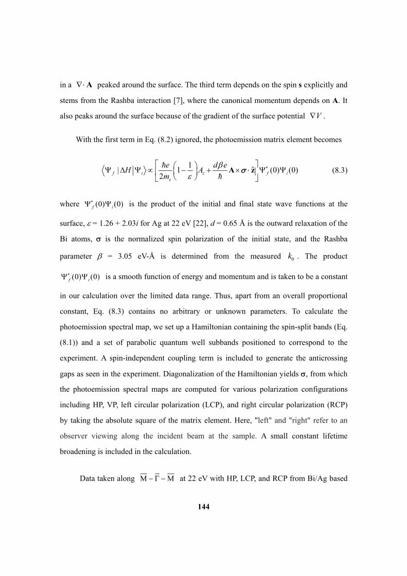
144
in a A peaked around the surface. The third term depends on the spin s explicitly and
stems from the Rashba interaction [7], where the canonical momentum depends on A. It
also peaks around the surface because of the gradient of the surface potential V .
With the first term in Eq. (8.2) ignored, the photoemission matrix element becomes
1ˆ| 1 (0) (0)
2f i z f ie
e d eH A
m
A z
(8.3)
where (0) (0)f i is the product of the initial and final state wave functions at the
surface, = 1.26 + 2.03i for Ag at 22 eV [22], d = 0.65 Å is the outward relaxation of the
Bi atoms, is the normalized spin polarization of the initial state, and the Rashba
parameter = 3.05 eV-Å is determined from the measured 0k . The product
(0) (0)f i is a smooth function of energy and momentum and is taken to be a constant
in our calculation over the limited data range. Thus, apart from an overall proportional
constant, Eq. (8.3) contains no arbitrary or unknown parameters. To calculate the
photoemission spectral map, we set up a Hamiltonian containing the spin-split bands (Eq.
(8.1)) and a set of parabolic quantum well subbands positioned to correspond to the
experiment. A spin-independent coupling term is included to generate the anticrossing
gaps as seen in the experiment. Diagonalization of the Hamiltonian yields , from which
the photoemission spectral maps are computed for various polarization configurations
including HP, VP, left circular polarization (LCP), and right circular polarization (RCP)
by taking the absolute square of the matrix element. Here, "left" and "right" refer to an
observer viewing along the incident beam at the sample. A small constant lifetime
broadening is included in the calculation.
Data taken along M M at 22 eV with HP, LCP, and RCP from Bi/Ag based

145
on a 20-ML Ag film are presented in Figs. 8.3(a)-8.3(c). The calculated band dispersions
(Fig. 8.3(d)) show the surface bands, the quantum well bands, and the anticrossing gaps.
Remaining in the gaps are the quantum well states with the opposite spin orientation than
the crossing surface bands. With kx pointing along M , the only nonzero spin
component is y. The xz plane, which contains the incident photon beam, is a mirror
plane of the sample. As a result of the overall symmetry of the system, LCP is equivalent
to RCP, and there should not be any circular dichroism. Indeed, the LCP and RCP data
appear to be identical, and the surface band with spin polarization along y is much
more intense than the other surface band with spin polarization along y . The same
intensity imbalance is evident in the HP data. A calculated photoemission map (Fig.
8.3(e)) for HP shows indeed an intensity imbalance in agreement with the data. By
contrast, the same calculation, assuming no spin-orbit coupling by setting to zero,
yields a map with equal intensities for the two bands (Fig. 8.3(f)). The results indicate
that the intensity imbalance between the two bands is a spin effect, despite the lack of
circular dichroism.
Circular dichroism becomes apparent for measurements along K K , for
which the system no longer possesses mirror symmetry about the xz plane. While the HP
map (Fig. 8.4(a)) shows equal intensities for the two spin-split bands, the LCP and RCP
maps (Figs. 8.4(b-c)) show different intensities. In fact, the LCP and RCP maps appear to
be left-right mirror images of each other about . To quantify this difference, we define
a dichroic function
-L R
L R
I I
I I
(8.4)
where IL,R are the photoemission intensities for LCP and RCP, respectively. The

146
experimental results are presented in Fig. 8.4(d), where red and blue colors indicate
positive and negative values of , respectively. The maximum value of is about ±30% at
the top of each surface band and the sign of is opposite for the two bands. Fig. 8.4(e)
shows the theoretical spin polarization inherited from the Rashba split surface states.
States with spin polarization along + x and – x directions are colored in red and blue,
respectively. Near the hybridization gaps, the states transform smoothly from surface-like
to bulk-like and the hybrid states are partially spin polarized. The calculated dichroic
function (Fig. 8.4(f)) is in excellent agreement with the experimental pattern. The
maximum value of is ±38.9% from the calculation. It is somewhat higher than the
experimental value; the difference can be attributed to the less than perfect polarization
state of the LCP and RCP light and possibly to sample imperfections.
8.4 Transition matrix elements for surface photoemission
Derivation of the coefficients of the two terms in Eq. (8.3) is sketched here. In the
classical limit, the product of the dielectric function and the z-component of the vector
potential Az is continuous across the surface, while the in-plane components of the
vector potential Ax,y are continuous. Because is discontinuous at the surface, Az must be
discontinuous. As a result, A is proportional to z with the surface located at z =
0. The matrix element involves an integration over all space. The result contains the
product of the initial and final state wave functions at the surface, (0) (0)f i .
Quantum mechanically, the delta function z is somewhat broadened with a width of
about the screening length. For the second term in Eq. (8.3) arising from the Rashba
interaction, the surface potential V has a finite jump at the surface over a distance of
about the outward relaxation of the Bi atoms (d = 0.65 Å for Bi/Ag). Its gradient, V , is
also a somewhat broadened delta function. After integration, it, too, contains the same

147
(0) (0)f i factor. This factor can be taken to be part of the normalization factor and
does not enter into the final calculations. The dichroic behavior is entirely determined by
the relative strengths of the two terms. The photocurrent is given by
22 22 . .z y x x y z y x x yI C A D A A C DA A A c c (8.5)
where 1 2 eC e m , D e d , and , ,x y zA are the components of the vector
potential. The Rashba parameter equals 3.05 eV-Å for Bi/Ag. Under typical
conditions with the usual lifetime broadening of the states, circular dichroic effects
become difficult to detect with the Rashba coefficient smaller than about 0.5 eV-Å.
8. 5 CARPES spectra of Ag quantum well states
For comparison, we have performed similar measurements of a 20-ML Ag film
prepared on Si(111)-(7x7) without Bi. Photoemission maps taken along M M at
22 eV with HP, VP, LCP, and RCP are presented in Fig. 8.5. The parabolic bands are
derived from quantum well states; the emission feature right around the Fermi level near
is derived from a Ag(111) Shockley surface state. The photoemission intensities of the
surface state and the quantum well states are close to zero for VP. The reason is that the
surface-photoemission term related to A vanishes with Az = 0. The Rashba term is
negligible because of a very weak spin-orbit coupling in Ag. The dipole term is negligible.
The HP, LCP, and RCP maps look the same; the quantum-well bands appear symmetric in
intensity. As expected, there is no circular dichroism.
8.6 First-principles study of a single Bi/Ag layer
The Rasha-Bychkov model is a successful phenomenological theory describing the
spin splitting induced by the structural inversion asymmetry (SIA) in 2D electron systems.

148
The model was originally developed for semiconductor heterostructures. At interfaces,
inversion symmetry is naturally broken and the bound states there experience an effective
electric field normal to the interface. The RB model can be described by an effective
Hamiltonian:
( ) ( )RB R z R y x x yH k k k e (8.6)
where R is the Rashba parameter. The resulting energy dispersion of a nearly free
electron gas is
22
0( ) ( )2
E k k Em
k , (8.7)
where m is the effective mass, 2Rk m is the offset by which the parabola is
shifted away from the high symmetry point, and 0E is an offset in energy. The energy
dispersion of a Rashba split nearly free electron gas is schematically shown in Fig. 8.6.
The same argument can be applied to the surface states too. A noted example for a
Rashba spin split 2D electron gas is the surface states at the Au(111) surface [23,24,25].
The SIA is due to the confinement of the surface states on one side by the surface barrier
and on the other side by the bulk band gap of Au. The momentum offset k for Au(111)
surface is 0.012 Å -1 [26], which is considerably larger than the 0.0007 Å -1 momentum
offset of Ag (111) surface. The larger spin splitting of Au (111) can be attributed to the
fact that Au is heavier than Ag and thus has much stronger atomic spin-orbit coupling.
The surface alloy Bi/Ag(111) have been identified with an unexpectedly large spin
splitting in its surface band structure ( 0.13k Å -1). Considering the similar atomic
weights of Au and Bi, the enhanced spin splitting in the Bi/Ag(111) surface alloy is a
consequence of the prominent corrugation in the surface structure. Therefore, both atomic

149
spin-orbit coupling and the surface corrugation are essential for realizing huge spin
splitting in the surface states. The prominent outward relaxation of Bi atoms relative to
the Ag atomic plane produces not only a large vertical potential gradient, the key
ingredient for Rashba splitting, but also an anisotropic in-plane SIA [27]. This additional
SIA within the confinement plane leads to a hexagonal warping in the surface band
dispersion [28] as well as out-of-plane spin polarization. Extending the RB model to
include the in-plane potential gradient results in a strong enhancement of the spin
splitting. Previous study [29] pointed out that the wavefunctions of surface states are
strongly localized in the topmost layer, i.e., in the alloy layer while the supporting
substrate carries at most 22% of the spectral weight. Therefore, the substrate atoms have a
negligible effect on the spin splitting of the surface states. For the sake of simplicity, we
perform a systematic first-principles study of the alloy layer without considering the
substrate Ag layers.
The band structure of a Bi/Ag surface alloy layer is shown in Fig. 8.7. In the
calculation each Bi atom sits in a 3-fold hollow site above the Ag atomic plane at 0.64 Å,
a value experimentally determined by IV-LEED [15]. Around the zone center there
are two sets of Rashba split surface bands near the Fermi level. The state slightly below
the Fermi energy has mainly spz character at the Bi site. The band above the Fermi level
dispersing downward along the ΓM and ΓK directions has almost purely Bi px,y
character [30]. The Rashba momentum offset in the spz band is 0.144 Å-1 which is very
close to the experimental value 0.13 Å-1 and this justifies the negligible effect of the
substrate layers on the Rashba splitting in the surface bands.
The buckling geometry of the surface alloy layer is essential for the spin splitting in
the surface bands. Without the surface corrugation, the Bi atoms sits within the Ag atomic
plane and the overall structure is space-inversion symmetric with respect to each Bi atom.

150
There will be no spin splitting in this case due to the simultaneous presence of the space
inversion symmetry and the time reversal symmetry. When the Bi atoms get relaxed out
of the Ag plane, the alloy layer loses the space inversion symmetry and as a consequence
the spin splitting shows up in the surface bands. On the other hand, if the Bi atoms are
pulled too far away from the Ag plane, the effective coupling between Bi orbitals and Ag
orbitals vanishes. The system is equivalent to two isolated layers of Bi and Ag atoms and
each atomic layer (Bi or Ag) is space-inversion symmetric. Under this isolation limit the
spin degeneracy gets recovered. Therefore, there must be an optimal buckling parameter
d to yield the largest spin splitting. The calculated band dispersion of the surface alloy
layer with different buckling parameters is plotted in Fig. 8.8. The spin splitting in the px,y
bands grows gradually from zero as the Bi atoms moves out of the Ag plane and it
reaches the maximum value ~ 0.9 Å-1 when the Bi atoms are 0.8 Å above the Ag planes.
As Bi moves even further away, the Rashba splitting decreases as a result of the
diminishing coupling of Bi with Ag. The dependence of the spin splitting on the buckling
parameter d is shown in Fig. 8.9 (b). The response of the spin splitting in the spz bands to
the displacement of Bi atoms is much more complicated due to the hybridizing effect of
the spz bands with their neighboring bands. In addition, the surface alloy layer with d
0.6 Å has the lowest surface energy as shown in Fig. 8.9 (a). The calculated stable
relaxation of Bi atoms is very close to the experimental value 0.64 Å for the Bi/ AG
surface alloy on the Ag(111) surface indicating again that the Ag substrate has little effect
on the electronic structure of the surface alloy layer.
The other important parameter determining the Rashba splitting of the surface alloy
layer is the atomic spin-orbit coupling (SOC). There are two components of the surface
alloy: Bi and Ag. It’s instructive to learn how the SOCs of Bi and Ag affect the band
structure of the surface alloy individually. Fig. 8.10 presents the band structures of a
single layer Bi/Ag surface alloy with the SOCs of Ag and Bi atoms turned on and off

151
alternately. The band dispersion with only Ag SOC (Fig. 8.10 (c)) is very similar to that
without any atomic SOC (Fig. 8.10(a)) except the small energy gap ~0.1 eV between the
top two bands near the zone center . The Bi SOC alone, by contract, can induce the
giant Rashba splitting of the Bi/Ag surface alloy, which is demonstrated by comparison
of Fig. 8.10(b) and Fig. 8.10(d). Therefore, the strong atomic SOC of the heavy element
Bi is crucial for achieving the giant Rashba splitting in the Bi/Ag surface alloy while the
Ag atoms act as a messenger to transfer the Bi SOC to the surface states of the alloy
systems by coupling to the Bi atoms. Calculations of the band structure at various levels
of SOC strength (Fig. 8.11(a)) ranging from 0 to 100% confirm the key role played by the
atomic SOC in the Rashba splitting of the surface alloy. The linear dependence of the
Rashba momentum shift k in the spz bands as shown in Fig. 8.11(b) is in good
accordance with Petersen and Hedegard’s tight-binding description of Rashba splitting of
sp-derived surface states [31]. The tight bind model gives the Rashba coupling ( R in Eqn.
8.6) is proportional to the atomic spin-orbit interaction as well as the surface potential
gradient which breaks the space inversion symmetry.
Previous electronic structure calculation [1] has shown that the Bi/Ag surface states
are much more tightly localized in the topmost layer than the Ag(111) or Au(111)
Shockley surface states. Therefore, the giant Rashba splitting and the Bi/Ag surface band
dispersion are not directly affected by the thickness of the Ag supporting film. That’s why
our calculation for only the surface alloy layer can yield the essential physics in this
prototypical Rashba system. We also performed calculation for the surface alloy system
with the Ag supporting layers included to demonstrate the substrate effect of Ag films.
The results for the Bi/Ag surface alloy sitting on a 1ML Ag film and a 9ML Ag film are
shown in Fig. 8. 12(a) and (b), respectively. Apparently the Ag substrate doesn’t affect the
magnitude of the Rashba splitting in the surface band dispersion, but it introduces to the
system the Ag sp quantum well states which are hybridized with the spin split surface

152
states. Through this hybridization mechanism, the Ag quantum well states gain finite spin
polarization [4,18].
Isostructural surface alloy systems Sb/Ag(111) and Pb/Ag(111) have been
experimentally realized [20,30]. The SOC induced spin splitting ( 0.005zspk Å-1) in the
Sb/Ag(111) surface alloy is strongly reduced compared with the Bi case because of the
much weaker atomic SOC and the less outward relaxation of Sb atoms ( 0.11d Å) [15].
The Pb/Ag(111) surface states, on the other hand, show up a considerably large Rashba
splitting ( 0.03zspk Å-1). This is because Pb is a high-Z element and the surface
buckling ( 0.46d Å) is more prominent than the Sb case. We calculated the band
dispersion relation of the surface alloy layer with different adatoms (Sb, Pb and Bi) under
the same structural geometry. When the surface corrugation is small, all three surface
alloy layers have little spin splitting in their surface bands as shown in Figs. 8. 13 (a-c).
For a larger surface buckling d=0.64 Å, the Rashba momentum shift in the spz surface
bands is 0.035, 0.087 and 0.144 Å-1 for Sb/Ag, Pb/Ag and Bi/Ag, respectively. The
atomic SOCs in Sb 5p orbitals ( 5 (Sb)p ), Pb 6p orbitals ( 6 (Pb)p ) and Bi 6p orbitals
( 6 (Bi)p ) are 0.4, 0.91 and 1.25 eV, respectively. The ratio of Rashba splitting in three
systems is 0.24:0.60:1 and the ratio of the atomic SOCs is 0.32:0.73:1. Therefore, the
Rashba splitting in the three cases roughly reflects the relative strength of the atomic
SOC of the three adatoms. Comparing to the ratio of the atomic SOCs, the ratio of the
Rashba splitting of Sb/Ag (Pb/Ag) to the Bi/Ag case is slightly smaller, which can be
attributed to the smaller atomic radius of Sb (Pb) and thus the weaker coupling between
the Sb and Ag atoms within the surface alloy layer.
8.7 Conclusion
The Bi/Ag surface alloy possesses giant Rashba spin splitting in its surface bands,

153
which makes it a potential platform for future applications of spintronics and quantum
computation. We performed a systematic first-principles calculation for the surface alloy
layer to investigate the dependence of the Rashba spin splitting on the atomic spin-orbit
coupling and the surface corrugation. The results shows that the Rashba splitting is
proportional to the atomic SOC, and it saturates at certain surface buckling parameter due
to the trade-off between the breaking of space inversion symmetry and the interatomic
coupling strength within the surface alloy layer. In the case of Bi/Ag, the optimal
relaxation length is 0.8d Å. Our work offers a guideline for searching two dimensional
systems with large Rashba spin splitting.
We also did a circular ARPES measurement on the Bi/Ag surface alloy. The good
agreement between experiment and our calculation under various experimental conditions
is a strong testimony of the theoretical treatment. The results confirm the strong spin
texture of Bi/Ag including the complex pattern of interference between the spin-polarized
surface states and the unpolarized quantum well states. A key finding is that the
surface-photoemission term derived from a nonzero A and the A-dependent part of
the Rashba interaction can interfere with each other and are both important for
understanding our results. The A term has been largely ignored in prior publications,
and our analysis here is the first quantitative study of spin-orbit coupling effects taking
both terms into account. The methodology developed here should be valuable for
unraveling the electronic structure of complex systems including topological insulators,
heavy-element compounds, superconductors, and strongly correlated systems in general
[32,33,34,35].
References:
[1] C. Ast et al., Phys. Rev. Lett. 98, 186807 (2007).

154
[2] H. Bentmann et al., Europhys. Lett. 87, 37003 (2009).
[3] A. C. Potter and P. A. Lee, Phys. Rev. Lett. 105, 227003 (2010).
[4] K. He et al., Phys. Rev. Lett. 104, 156805 (2010).
[5] F. Meier et al., Phys. Rev. B 77, 165431 (2008).
[6] V. B. Zabolotnyy et al., Phys. Rev. B 76, 024502 (2007).
[7] Y. H. Wang et al., Phys. Rev. Lett. 107, 207602 (2011).
[8] Y. Liu et al., Phys. Rev. Lett. 107, 166803 (2011).
[9] Y. Ishida et al., Phys. Rev. Lett. 107, 077601 (2011).
[10] T. Miller, W. E. McMahon and T.-C. Chiang, Phys. Rev. Lett. 77, 1167 (1996).
[11] T. Miller, E. D. Hansen, W. E. McMahon and T.-C. Chiang, Surf. Sci. 376, 32
(1997).
[12] E. D. Hansen, T. Miller and T.-C. Chiang, Phys. Rev. Lett. 78, 2807 (1997).
[13] Y. A. Bychkov and E. I. Rashba, Sov. Phys. JETP Lett. 39, 78 (1984).
[14] T.-C. Chiang, Surf. Sci. Rep. 39, 181 (2000).
[15] I. Gierz et al., Phys. Rev. B 81, 245430 (2010).
[16] Y. A. Bychkov and E. I. Rashba, J. Phys. C 17, 6039 (1984).
[17] E. Frantzeskakis et al., Phys. Rev. Lett. 101, 196805 (2008).
[18] K. He et al., Phys. Rev. Lett. 101, 107604 (2008).
[19] S.-J. Tang et al., Phys. Rev. Lett. 96, 216803 (2006).

155
[20] L. Moreschini et al., Phys. Rev. B 79, 075424 (2009).
[21] G. Bihlmayer, S. Blügel and E. V. Chulkov, Phys. Rev. B 75, 195414 (2007).
[22] H. J. Hagemann, W. Gudat and C. Kunz, J. Opt. Soc. Am. 65, 742 (1975).
[23] S. Lashell, B. A. McDougall, and E. Jensen, Phys. Rev. Lett. 77, 3419 (1996).
[24] F. Reinert, J. Phys: Condens. Matter 15, S693 (2003).
[25] J. Henk, A. Ernst and P. Bruno, Phys. Rev. B 68, 165416 (2003).
[26] H. Cercellier et al., Phys. Rev. B 73, 195413 (2006).
[27] J. Premper et al., Phys. Rev. B 76, 073310 (2007).
[28] L. Fu, Phys. Rev. Lett. 103, 266801 (2009).
[29] L. Moreschini et al., Phys. Rev. B 80, 035438 (2009).
[30] D. Pacile et al., Phys. Rev. B 73, 245429 (2006).
[31] L. Petersen and P. Hedegård, Surface Science 459, 49 (2000).
[32] M. Z. Hasan and C. L. Kane, Rev. Mod. Phys. 82, 3045 (2010).
[33] X.-L. Qi and S.-C. Zhang, Rev. Mod. Phys. 83, 1057 (2011).
[34] I. Gierz et al., Phys. Rev. Lett. 103, 046803 (2009).
[35] K. Yaji et al., Nat. Commun. 1:17 (2010).

156
Figures:
Figure 8.1. (a) Structures of Bi(Sb)/Ag Surface Alloys and photoemission data from
Bi/Ag. (a) Sample configuration. (b) and (c) Top and side views of the lattice structures
of the surface alloys. Blue balls indicate Bi or Sb atoms and yellow balls stand for silver
atoms. (d) Surface Brillouin zones of the surface alloy and Ag(111) films. (e) A map
taken from Bi/Ag based on a 20-ML Ag film. The spectrum is mapped using 22 eV
horizontally polarized photons.
5.01 Å
d = 0.65 Å for Bi/Ag, 0.10 Å for Sb/Ag
d
8.68 Å
Si(111)-(7x7)
Ag(111)
Bi(Sb)/Ag
max
min
1 st 2 nd KMM0.0
0.5
1.0
1.5
1Åk0.5 0.0 1.0 1.50.5
Bi/Ag
M'
K'
K
M
Bi(Sb)/Ag
Ag
(a)
(c) (d)
(b)
(e)
E(eV)
1
1
M 0.73A
K 0.84A

157
Figure 8.2. Experimental geometry and ARPES maps from Bi(Sb)/Ag(111) surface alloys
taken with HP light at 22 eV. (a) Experimental geometry. The normal of the sample
surface is along z and the vertical direction is along y in the laboratory frame of
reference. (b) Schematic band dispersion relations and spin textures of Bi/Ag; Sb/Ag has
similar band dispersion relations but the spin splittings are much smaller and not apparent
in the data. (c) and d) Photoemission results taken along K K and M M
directions, respectively, from Sb/Ag based on a 22-ML Ag film. (e) Photoemission results
taken along M M from Bi/Ag based on a 20-ML Ag film.
(a)
K
HPA
Mxk
yk
Photon VPA
zk
ˆks z
E
- zs p
k-x yp p
ˆ+ks z
(b)
max
min
1Åk
M M 0.0
0.5
0.2
1.0
1.5
0.0 0.2 0.00.2 0.20.2 0.0 0.2
K K M M
Bin
ding
Ene
rgy
(eV
) (e)(d)(c)

158
Figure 8.3. Photoemission results taken from Bi/Ag based on a 20-ML Ag film. The data
were taken along M M using 22-eV photons and (a) HP, (b) LCP, and (c) RCP
polarization configurations. (d) Calculated band structure showing the hybridization of
s-pz surface bands with quantum well bands of the Ag film. (e) Calculated photoemission
map for HP. (f) Calculated photoemission map for HP assuming that the
spin-orbit-coupling contribution to surface photoemission is zero.
1Åxk
Bin
ding
Ene
rgy
(eV
)
max
min
M M
0.0
0.5
0.2
1.0
1.0
0.0 0.2
0.0
0.5
0.2-0.20.2 0.0 0.2 0.0
HP LCP RCP(a) (b)
(d)
(c)
(e) (f)

159
Bin
ding
Ene
rgy
(eV
)
Figure 8.4. Photoemission results taken from Bi/Ag based on a 20 ML Ag film. The data
were taken along K K using 22-eV photons and (a) HP, (b) LCP, and (c) RCP
polarization configurations. (d) Dichroic function extracted from the data. (e) Calculated
band structure weighted by the spin polarization inherited from the Rashba split surface
states using red and blue colors. (f) Calculated dichroic function.
K K
1Åyk
0.0
0.5
1.0
1.0
0.0
0.5
0.5
1.0
0.0
0.0 0.2 0.0 0.20.2 0.2
LCP
RCP
HP max
min
xs
xs
(a)
(b)
(d)
(c)
(e)
(f)

160
Figure 8.5. Photoemission results taken from a 20-ML Ag film along M M using
22 eV photons. The data are for (a) HP, (b) VP, (c) LCP, and (d) RCP polarization
configurations.
RCP
M M
(a) (b)
(c) (d)
1Åxk
0.0
2.0
1.0
2.0
0.0
1.0
0.2-0.20.0 0.2 0.0
HP
LCP
VP B
indi
ng E
nerg
y (e
V)
max
min
0.4-0.40.4-0.2-0.4

161
Spin degenerate Rashba splitting
E
/ /k / /k
E
Figure 8.6. Schematic energy dispersion of a Rashba split nearly free electron gas.
k

162
K MM
0.0
1.0
2.0
1.0
2.0
E(eV)
1k(A )
1.0 0.5 0.0 0.5
d 0.64A
1shiftk 0.144A
1EXPk 0.13A
x,yp
zsp
Figure 8.7. Band structure of a single layer Bi/Ag surface alloy without Ag supporting
layers.

163
Figure 8.8. Band structure of a single layer Bi/Ag surface alloy with different buckling
parameter d.
d 0.0A 0.2A 0.4A 0.6A
0.8A
1.8A1.6A
1.4A1.2A1.0A
2.0A
E(eV)
M M M MM M M M2.0
1.0
0.0
1.0
2.0
2.0
1.0
0.0
1.0
2.0
2.0
1.0
0.0
1.0
2.0

164
Figure 8.9. (a) Surface energy of a single layer Bi/Ag surface alloy as a function of the
buckling parameter d. (b) The Rashba momentum shift in the px,y bands as a function of d.
Buckling d(A)
Surface
Energy
0.0 1.0 2.0
SEmind 0.6A
EXPd 0.64A
(a)
(b)
Buckling d(A)0.0 0.4 1.20.8
0.00
0.05
0.10
,
1(A )x ypk
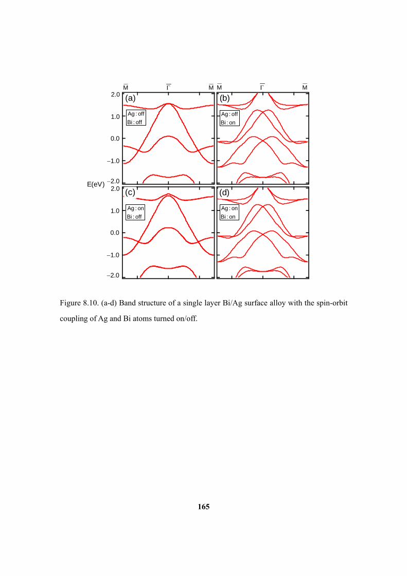
165
Figure 8.10. (a-d) Band structure of a single layer Bi/Ag surface alloy with the spin-orbit
coupling of Ag and Bi atoms turned on/off.
(a) (b)
(c) (d)
Ag : off
Bi : off
Ag : off
Bi : on
Ag : on
Bi : off
Ag : on
Bi : on
E(eV)
M M M M2.0
1.0
0.0
1.0
2.02.0
1.0
0.0
1.0
2.0

166
Figure 8.11. (a) Band structure of a single layer Bi/Ag surface alloy with different
spin-orbit coupling. (b) Dependence of the Rashba momentum shift in the spz bands on
spin-orbit coupling.
0
50%
100%
60%
10% 20%
70%
80%
30%
40%
90%
(a)
(b)
E(eV)
M M M MM M M M2.0
1.0
0.0
1.0
2.0
2.0
1.0
0.0
1.0
2.0
2.0
1.0
0.0
1.0
2.0
SOC (%)
0.15
0.10
0.05
60
0.00
0 20 40 10080
1(A )zspk

167
Figure 8.12. Band structure of the Bi/Ag surface alloy sitting on (a) 1 ML Ag(111) slab
and (b) 9 ML Ag(111) slab.
(a) (b)
M M M M
E(eV)
2.0
1.0
0.0
1.0
2.0

168
Figure 8.13. (a-f) Band structure of a single layer Sb/Ag, Pb/Ag and Bi/Ag surface alloy
with different buckling parameters d.
Sb/Ag Pb/Ag
d=0.11A
d=0.64A
Bi/Ag
Z=51 Z=82 Z=83
(a) (b) (c)
(d) (e) (f)
M M
E(eV)
2.0
1.0
0.0
1.0
2.0
M M M M
2.0
1.0
0.0
1.0
2.0

169
9 Summary and Outlook
This thesis has focused primarily on ARPES and first-principles studies of the
topological Sb, Bi2Te3 and Bi2Se3 thin films. In addition, two systems of technological
importance, the Bi thin film and the Bi/Ag surface alloy, have been investigated. Many
observed phenomena such as the metastability of Bi thin films and the quantum tunneling
gap at the Dirac point of the topological surface bands are direct manifestations of
quantum size effects, intrinsic to thin films.
Atomically uniform Sb films have been successfully fabricated on the Si(111)
substrate. A Bi buffer layer or a a Bi-terminated Si(111)- 3 3 30R surface
reconstruction is essential for the smooth growth of the epitaxial Sb films. The ARPES
spectra have shown clearly the nontrivial topological order of the Sb films as well as a
smooth passage from spin-polarized surface states to spin-unpolarized quantum well
states. Moreover, ARPES mapping of a 4-BL Sb film has shown no tunneling-induced
energy gap at the Dirac point of the topological surface bands, contrary to a theoretically
predicted one for a freestanding film. The observed robust Dirac cone is the result of a
strong interfacial bonding between the film and the substrate. The interfacial interaction
lifts the energy degeneracy of the surface states on the opposite faces of the film and thus
suppresses quantum tunneling effect.
Topological order and topological surface states are the intriguing characteristics of
topological materials. Even though the topological order is a robust quantity protected by
time reversal symmetry, the detailed dispersion of topological surface states is be very
sensitive to the boundary conditions. Our first-principles calculations for Bi2Te3 and
Bi2Se3 thin films have shown, upon hydrogen termination of either face of the slab, the
Dirac cone associated with this face is replaced by three Dirac cones centered at M

170
points at the zone boundary. In addition, we have shown by first-principles simulations
for freestanding Bi2Se3 films that the topological surface states can disappear completely
in topological films even at large film thicknesses. This anomalous behavior occurs when
the effective SOC of the system is tuned close to the topological critical point and it can
be suppressed in an asymmetric film of Bi2Se3 with one face terminated by H.
Our photoemission experiment on epitaxial Bi films has demonstrated the existence
of a metastable PC phase and a stable RH phase of Bi films over a wide range of film
thickness from 20 to ~100 Å. The PC-RH metastability range is unusually wide, which
can be understood in terms of a near degeneracy of the bulk energies of the two phases
and a surface-nucleation process that facilitates the formation of the metastable phase. We
have also performed a circular ARPES measurement on the Bi/Ag surface alloy, a system
with a giant Rashba spin splitting. A theoretical approach has been developed to build up
a connection of the observed dichroic pattern with the spin texture of the surface alloy.
The key finding is that the surface-photoemission term derived from a nonzero A
and the A-dependent part of the Rashba interaction can interfere with each other and are
both important for understanding our results. In addition, a systematic first-principles
calculation for the surface alloy layer has been done to examine the dependence of the
Rashba spin splitting on the atomic spin-orbit coupling and the surface corrugation. The
results have indicated that the Rashba splitting is proportional to the atomic SOC and
saturates at certain surface buckling parameter due to the trade-off between the breaking
of space inversion symmetry and the interatomic coupling strength within the surface
alloy layer. Our work will shed some light on the search of two dimensional systems with
large Rashba spin splitting.
In this dissertation research, atomically uniform thin films of Sb, Bi, the topological
insulator Bi2Te3 and the surface alloy Bi(Sb)/Ag(111) have been successfully fabricated
on semiconductor substrates. Their structural qualities have been examined by

171
experimental tools such as RHEED and LEED, and their electronic structures have been
thoroughly studied by ARPES and first-principles calculations. These thin films and
surface alloys have great potential for practical device applications of spin-related
electronics and quantum computation. To further test the electronic properties, detailed
transport measurements are needed. Weak anti-localization and anomalous Hall effect
stemming from topological order may have a profound impact on the transport properties
of atomically thin materials and device structures.
Electronic chirality and Berry’s phase are topics of central importance for
understanding unique electronic and spin properties of topological materials. Our work
on the Bi/Ag surface alloy has proven that the circular dichroic ARPES is a powerful
probe of the spin texture. This novel experimental method can be straightforwardly
utilized to examine electronic chirality and Berry’s phase of topological materials. In
addition, the Bi/Ag surface alloy is the key ingredient of Potter and Lee’s proposal for
realizing the elusive Majorana states. In their experimental scheme, a ferromagnetic
insulating EuO thin film is used induce a Zeeman splitting to surface electrons of the
Bi/Ag layer. A px+ipy pairing can be induced by proximity to a conventional
superconductor like Nb. A crucial condition for this junction is that the thickness of the
Ag film cannot exceed the superconducting coherent length. We have obtained a well
ordered Bi/Ag 3 3 surface on atomically uniform Ag thin films by MBE method.
The thickness of epitaxial Ag films is several nanometers, which guarantees the
effectiveness of the proximity effect. The deposition of ferromagnetic insulating EuO thin
film can be achieved in an oxide MBE chamber. The major challenge will be to obtain
well-ordered Ag films on the surface of a conventional superconductor, since a smooth
Ag surface is the precondition for making the Bi/Ag surface alloy. Considerable
experimental effort will be required to optimize the structural quality of the surface alloy
as well as the superconducting proximity effect on the Bi/Ag surface states. The result
172
could provide an appealing possibility to realize Majorana fermions and a potential
platform for future topological quantum computation.

173
Appendices
Appendix A: Computational software: ABINIT
The computational software employed for the first-principles calculations in this
thesis is ABINIT [1,2]. Here is a brief introduction to this versatile software. ABINIT is a
package whose main program allows one to find the total energy, charge density and
electronic structure of systems made of electrons and nuclei (molecules and periodic
solids) within Density Functional Theory (DFT), using pseudopotentials and a planewave
or wavelet basis. ABINIT also includes options to optimize the geometry according to the
DFT forces and stresses, or to perform molecular dynamics simulations using these forces,
or to generate dynamical matrices, Born effective charges, and dielectric tensors, based
on Density-Functional Perturbation Theory, and many more properties.
When heavy atoms like Bi are involved in the calculation, the spin-orbit coupling
(SOC) has to be taken into account. It’s very convenient to handle SOC in the framework
of ABINIT. The incorporation of SOC is accomplished through the relativistic LDA
approximation [3]. For atoms, the Dirac equation is solved and the 2(2l+1) l-channel
degeneracy is lifted according to the eigenvalues of the L+S operator (l+1/2 and l-1/2 of
degeneracy 2l+2 and 2l). After pseudization, the associated wave functions can be
recovered by adding to usual pseudo-potential projectors a spin-orbit term of the generic
form v l,s l,sr L S . Not all potentials include this additional term, but it turns out
that it is the case for all the HGH type pseudopotentials [4]. In a plane-wave calculation,
the wavefunctions will be two components spinors, that is will have a spin-up and a
spin-down component but these components will be coupled. This means the size of the
Hamiltonian matrix is quadrupled.

174
To run ABINIT, there are three types of files needed:
(1) A file specifying the names and directories of input and output files
(2) An input file providing detailed information about the calculation: the lattice
structure, the exchange-correlation functional, etc.
(3) Pseudopotential files
An example of the main input file is given below: the meaning of input variables are
indicated by the comments.
################################################################################
# A supercell of 4BL Sb(111) slab plus 4BL vacuum
# Computation of the band structure.
# First, a SCF density computation, then a non-SCF band structure calculation.
#Global setting
ndtset 2 # gives the number of data sets to be treated
ixc 1 # type of exchange-correlation functional
nspinor 2 # spin-orbit coupling switch
so_psp 2 # spinor of each atom
occopt 7 # occupation option
tsmear 0.01 # temperature of smearing
enunit 1 # energy units print in eV
prtwf 0 # option for printing wavefunction
chksymbreak 0 # check symmetry breaking
#Dataset 1 : usual self-consistent calculation
iscf1 7 # option for self-consistent field (SCF) cysles
kptopt1 1 # option for the automatic generation of k points,
ngkpt1 8 8 2 # k point grid taking into account the symmetry
nshiftk1 1 # number of shifts for k point grid
shiftk1 0.0 0.0 0.5 # shift of k points
prtden1 1 # Print the density, for use by dataset 2
toldfe1 1.0d-9 # tolerance on the difference of total energy, criterion for convergence
#Dataset 2 : the band structure
iscf2 -2 # non-self-consistent calculaiton
getden2 -1 # read the density from previous self-consistent part

175
kptopt2 -2
nband2 50 # number of bands to calculate
ndivk2 75 50 # number of divisions of the k lines
kptbounds2 1.0 0.5 0.0 # M’-bar point, boundaries of k points
0.0 0.0 0.0 # Gamma-bar point
0.5 0.0 0.0 # M-bar point
tolwfr2 1.0d-12
#Definition of the unit cell
acell 3*8.127145312 # scaling of unit cell lattice vectors, in Bohr
rprim 1.0 0.0 0.0 # film primitive vectors (to be scaled by acell)
0.5 sqrt(0.75) 0.0
0.0 0.0 6.9583 # thickness: 4BL Sb(111)+4BL vacuum
#Definition of the atom types
ntypat 1 # There is only one type of atom
znucl 51 # The keyword "znucl" refers to the atomic number of the
# possible type(s) of atom. Here, the only type is Antimony (Sb)
#Definition of the atomic coordinates
natom 8 # number of atoms in unit cell
typat 8*1 # All possible atoms are type 1.
xred 0.0 0.0 0.00 #1 Sb, reduced coordinates of atom
1/3 1/3 0.0502 #2 Sb
2/3 2/3 0.125 #3 Sb
0.0 0.0 0.1752 #4 Sb
1/3 1/3 0.250 #5 Sb
2/3 2/3 0.3002 #6 Sb
0.0 0.0 0.375 #7 Sb
1/3 1/3 0.4252 #8 Sb
nstep 200 # Maximal number of SCF circles
ecut 15 # Maximal kinetic energy cut-off, in Hartree
################################################################################

176
Appendix B: Rhombohedral lattices of Bi, Sb, Bi2Te3 and Bi2Se3
Bulk Bi, Sb, Bi2Te3 and Bi2Se3 have the rhomohedral structure. The three primitive
vectors of the lattice are
1
2
3
( / 2, 3 / 6, / 3),
( / 2, 3 / 6, / 3),
(0, 3 / 3, / 3).
a a c
a a c
a c
a
a
a
(B1)
Here a and c are the lattice constants in the hexagonal unit cell. The corresponding
reciprocal lattice vectors, defined by 2i j ij a b , are given as
1
2
3
( 1, 3 / 3, ) ,
(1, 3 / 3, ) ,
(0,2 3 / 3, ) ,
b g
b g
b g
b
b
b
(B2)
with
/
2 / .
b a c
g a
(B3)
The lattice structure of Bi and Sb is composed of two interpenetrating, diagonally
distorted face-centered-cubic lattices with two atoms per unit cell. The relative position of
the two basis atoms is given by
(0,0,2 )d c . (B4)
The lattice parameters for Bi and Sb are listed in Table B1 [5,6], and the unit cell for Bi
and Sb is shown in Fig. B1 [7].
The Bi2Se3 family of compounds has a layered structure with five atomic layers as a
basic unit, namely a quintuple layer (QL) [8]. As shown in Fig. B2(a), Se2 is taken to be
the origin (0, 0, 0) of the unit cell; then two Bi atoms are at ( , and two Se1

177
are at ( , , defined in the unit of primitive vectors. All the experimental lattice
constants for the Bi2Se3 family of compounds are listed in Table B2 [9]. Fig. B2(c) shows
the 3D Brillouin zone (BZ) and the 2D surface BZ of Bi2Se3. (0, 0, 0), L( , 0, 0) ( 3),
F( , , 0) ( 3) and Z( , , ) are eight time-reversal invariant momentum (TRIM)
points in the 3D BZ. and Z are projected onto , and L and F are projected onto M
in the surface BZ. and M ( 3) are four TRIM points in the surface BZ.

178
Appendix C: Surface States, Quantum Well States and Excited
States of Ag(111) films
We will revisit several key electronic properties of Ag(111) thin films in this section.
As discussed in Chapter 4, the spatial confinement results in quantization of the bulk
bands as shown in Fig. C1. The band structure of a 20 ML freestanding Ag(111) film is
replotted in Fig. C1(b). The energy of the calculated d bands is too high by ~ 2 eV
compared to the experimental data [10]. This is because LDA (or GGA) functionals tend
to over-delocalize electrons and as a consequence the one-site Coulomb repulsion is not
well accounted for. This problem is more severe for highly localized d and f electrons,
and it can be corrected by more sophisticated methods like DFT+U [11]. The band edge
of Ag along (111) direction is at ~ -0.3 eV, which allows the existence of surface states in
this narrow energy gap. The two bands grazing the Fermi level at in Fig. C1(b) are of
surface nature. The plane-averaged charge densities of the two surface states at are
shown in Fig. C2. Due to the finite thickness of the Ag film, the two surface states on the
opposite faces can couple with each other and form two hybridized states. One of the
hybridized states shows node at the film center in the charge density while the other
shows anti-node. There exists a tiny energy difference between two hybridized states due
to the hybridization. The top five waves plotted in Fig. C3(a) are the sp quantum well
states at starting from the one right below the surface states. The envelope functions
of those quantum wells states arise from the crystal potential. It can be explained as a
beating pattern involving two plane waves with wave vectors k and G-k, where G is the
primitive reciprocal lattice vector along [111]. The beating number can be derived
from the Bohr-Sommerfeld quantization rule,
2 2kNt n (C1)

179
where k is measured from the zone center, N is the number of atomic layers, t is the
monolayer thickness and is the total phase shift at surface and interface. Since the
momentum k ( k ) of those QWSs are very close to the zone boundary at
/ 3 /Lk t a ( a is the lattice constant of Ag), it’s more convenient to write the
quantization condition in terms of k ( /k t k ) measured from the zone boundary.
2 2k N t n (C2)
The quantum number ( N n ) are small values near the band edge. Specifically,
1 corresponds to the quantum well state closest to the band edge. also gives the
number of peaks in the envelope function of quantum well states.
The other waves in Fig. C3(a) correspond to the d states adjacent to the sp quantum
well states. Those charge densities exhibit fine structure which can be seen in those of sp
states. In Fig. C3(a) there are excited states with energy larger than 4 eV around the zone
center. Those excited states form discrete parabolic subbands as a result of the finite
vacuum thickness (dvac=10 ML) adopted in our DFT calculation. The eigenvalues and
wavefunctions of excited states in DFT have no clear physical meaning because DFT
refers only to the calculation of the total energy and charge density of the ground states.
Nevertheless DFT offers a qualitatively reliable estimate of excited states of the system.
The charge densities of excited states at are shown in Fig. C3(b). The wave at bottom
corresponds to the excited state with the lowest energy. The charge of this states lies
mostly within the Ag film except a tiny tail in vacuum. As the excitation energy increases,
the charge gradually leaks into the vacuum and eventually it forms standing wave in the
vacuum layer with a minor part left in the Ag film. For infinite vacuum, the excited states
have plane-wave form outside the film, and their wavefunctions are determined by the
boundary condition at the interface. This is consistent with the time-reversed-LEED-state
description of the final states in the theory of ARPES.

180
Appendix D: Topological Phase Transition in the Kane-Mele Model
In this section we will examine the Kane-Mele model of graphene [12,13]. At
sufficiently low temperature a single layer of graphene exhibits a quantum spin Hall
(QSH) effect with an energy gap generated by the intrinsic spin-orbit interaction. The key
idea is that the spin-orbit coupling (SOC) serves as an effective magnetic field in a way
such that spin-up and spin-down electrons feel opposite magnetic fields and as a
consequence the Hall currents for spin-up and spin-down electrons propagate in opposite
directions. In the QSH phase there exist a net spin current at the boundary without
breaking the time reversal symmetry. The honeycomb lattice structure, the Brillouin zone
and the band structure of graphene are shown in Fig. D1.
The tight-bind Hamiltonian of graphene is
† † †zKane Mele i j SO ij i j v i i i
ij iij
H t c c i c s c c c . (D1)
The first term is a nearest neighbor hopping term on the honeycomb lattice. The second
term is the mirror symmetric spin-orbit interaction which involves spin dependent second
neighbor hopping. Here 1 2ˆ ˆ(2 / 3)( ) 1ij z d d , where 1̂d and 2d̂ are unit vectors
along the two bonds the electron traverses going form site j to i. sz is a Pauli matrix
describing the electron’s spin. The third term is a staggered sublattice potential ( 1i ).
The projected 1D Brillouin zone along the zigzag direction can be found in Fig. D1(b).
The band structure for a zigzag ribbon of width 50 atomic chains is shown in Fig. D2. In
the case without SOC and the staggered potential, the quantum well subbands derived
from the band of graphene are stacked around K . In addition, there are two
degenerate edge bands with zero energy connecting the bulk states at two K points.

181
With nonzero staggered potential, an energy gap of size 2 v is opened and the two
edge bands are no longer degenerate. The SOC term in Eqn. D1 can also open an energy
gap at the Dirac point. The energy gap induced by SOC is equal to 3 3 SO . When both
SOC and the staggered potential are present, the energy gap is of magnitude
3 3 2SO v . For 3 3 / 2v SO , the gap is dominated by v , and the system is an
ordinary insulator. 3 3 / 2v SO describes a topologically distinct phase, the QSH
phase. Figs. D3(a-c) demonstrate those different topological phases. Both phases have a
bulk energy gap and edge states, but only in the QSH phase the edge states traverse the
energy gap in pairs. At the transition between the two phases, the energy gap closes,
allowing the edges states to “switch partners”. The band structure with solely SOC is
shown in Fig. D3(d). The edge states on the opposite boundaries are degenerate, and they
form “Dirac cones” centered at M . The phase diagram of the Kane-Mele model is
present in Fig. D4.
The intrinsic SOC gap in graphene is about 10 mK~1 K. The small energy gap
hinders the observation of the QHS effect. The Kane-Mele model has motivated great
research interest in a single layer of silicon and germanium, namely, silicene and
germanene. Those systems have stronger SOC, and therefore the QSH effect is easier to
observe in those atomic sheets. The reported SOC band gap is 1.55 meV (~18 K) for
silicene and 23.9 meV (277 K) for germanene [14].
To test the robustness of the topological order, a potential bias is put on the top
atomic chain of the topological graphene ribbon as schematically shown in Fig. D5(a).
The band structures with different edge potentials are plotted in Fig. D5(b). As the edge
potential bias increases, the energy of the top edge band is gradually lifted. When the top
edge band merges into the conduction band as illustrated in the third panel of Fig. D5(b),

182
the highest conduction subband is isolated from the bulk band region, and the states in
this band are pretty much trapped in the top atomic chain due to the large potential bias.
At the same time, the highest valence subband is pulled into bulk band gap and becomes
localized near the top edge. With sufficiently large potential bias, the top atomic chain is
essentially cut off from the ribbon, yielding a different atomic configuration at the top
edge. The altered boundary condition makes the top-edge “Dirac cone” centered at in
contrast with the unperturbed one at .
This simple tight-binding model gives essentially the same physics discussed in
Chapter 6. Below is the Matlab M-file for the calculation:
%%%%%%%%%%%%%%%%%%%%%%%%%%%%%%%%%%%%%%%%%%%%%%%%%
% The code is done in collaboration with Ching-Kai Chiu
clear all
% Band Structure of Kane-Mele Model along ZigZag direction
t=1; %hopping coefficient
lso=0.0; %spin orbit coupling
lr=0.0; %Rashba coefficient
lv=0.0; %staggered potential
eb=0.0; %edge potential bias
mf=0.0; %vertical magnetic field
L=50; % width of graphene ribbon
N=4*L; %dimension of matrix
% define unit cell, k space
a=1;
k=0;
count=1;
kmax=6.29;
kint=0.01;
M=zeros(N,N); % initializing matrix
while k < kmax
pp=exp(i*a*k);

183
ss=sin(a*k);
for nn=1:L
M(4*nn-3,4*nn-1)=(1+pp)*t;
M(4*nn-2,4*nn)=(1+pp)*t;
M(4*nn-3,4*nn-3)=lso*ss;
M(4*nn-2,4*nn-2)=-lso*ss;
M(4*nn-1,4*nn-1)=-lso*ss;
M(4*nn,4*nn)=lso*ss;
M(4*nn-3,4*nn)=i*lr*(0.25*(1+pp)+i*0.25*sqrt(3)*(1-pp));
M(4*nn-2,4*nn-1)=i*lr*(0.25*(1+pp)-i*0.25*sqrt(3)*(1-pp));
M(4*nn-3,4*nn-3)=M(4*nn-3,4*nn-3)+lv+mf;
M(4*nn-2,4*nn-2)=M(4*nn-2,4*nn-2)+lv-mf;
M(4*nn-1,4*nn-1)=M(4*nn-1,4*nn-1)-lv+mf;
M(4*nn,4*nn)=M(4*nn,4*nn)-lv-mf;
if (nn<L)
M(4*nn-1,4*nn+1)=t;
M(4*nn,4*nn+2)=t;
M(4*nn-3,4*nn+1)=i*0.5*lso*(-1+pp);
M(4*nn-2,4*nn+2)=i*0.5*lso*(1-pp);
M(4*nn-1,4*nn+3)=i*0.5*lso*(1-pp);
M(4*nn,4*nn+4)=i*0.5*lso*(-1+pp);
M(4*nn-1,4*nn+2)=i*0.5*lr;
M(4*nn,4*nn+1)=i*0.5*lr;
end
end
for mm=1:N
for nn=1:mm
M(mm,nn)=conj(M(nn,mm));
end
end
M(1,1)=M(1,1)+eb;
M(2,2)=M(2,2)+eb;
pict(count,:)=transpose(sort(eig(M)));
count=count+1;
k=k+kint;
end
figure(1)
plot(0:0.01:kmax,pict,'-k','linewidth',1.5)

184
axis([0, 6.29, -3, 3])
set(gca, 'XTick', [],'YTick', []);
line('XData',[0 6.29],'YData',[0 0],'color','r','LineStyle','-.','LineWidth',1.5)
line('XData',[pi*2/3 pi*2/3],'YData',[-3 3],'color','r','LineStyle','-.','LineWidth',1.5)
line('XData',[pi*4/3 pi*4/3],'YData',[-3 3],'color','r','LineStyle','-.','LineWidth',1.5)
%%%%%%%%%%%%%%%%%%%%%%%%%%%%%%%%%%%%%%%%%%%%%%%%%

185
Appendix E: Probing Berry’s Phase in Graphene by Circular
ARPES
Electronic chirality near the Dirac point is a key property of graphene systems [15].
The direction of the pseudospin vector in monolayer graphene tracks the rotation of the
electronic crystal momentum, resulting in a Berry's phase of π [16,17]. Our group has
observed the chiral property of graphene using circular ARPES [18]. The elegant ARPES
experiment was performed by my labmate Dr. Yang Liu. In the section we will give an
intuitive understanding of the experimental results.
The ARPES geometry is shown in Fig. E1(a). The sample is monolayer graphene
prepared on SiC. 30-eV photons are incident nearly in the normal direction of sample
surface. The vector potential of photon is
ˆ ˆ ˆ=A A Ax y z A x y z . (E1)
Under the experimental conditions, Az is negligibly small. Ignoring the contribution form
surface transition, which is proportional to 2
A z , the photoemission intensity is given by
the dipole transition probability
2| | ( )k kf i f iI E E A p . (E2)
Generally, the vector potential for elliptically polarized light is given by
0 ˆ ˆ=A (cos sin )A Ai A x y , (E3)
where tan Aφ is the ellipticity. 0, / 4, / 2 and 3 / 4A for HP, LCP, VP and RCP,
respectively.
The two-component electron wavefunction of monolayer graphene, close to the K
point, obeys the 2D Dirac equation,

186
( ) ( )Fiv E r r . (E4)
The wavefunction, in momentum space, for the momentum around the K point has the
form
/2
, /2
1( )
2
i
K i
e
e
k
kk (E5)
for K FH v kσ , where the signs correspond to the eigenenergies FE v k , that is,
for the and bands (bands above and below the Dirac point), and k is illustrated
in Fig. E1(b). Note that if the phase angle k is rotated by 2 , the wavefunction
changes sign indicating a phase of which, in the literature, is called a Berry’s phase.
This change of phase by under rotation is characteristic of spinors.
Fig. E1(c) shows ARPES results around the K point measured along the y direction
with LCP and RCP. Evidently, photons with different helicity selectively excite one of the
two branches of the Dirac cone with opposite pseudospin directions. Fig. E2 presents
typical constant energy maps of the π* and π bands of monolayer graphene, respectively,
using the four polarization configurations. For each band, the semicircular pattern rotates
counterclockwise in 90º steps in going from HP to LCP to VP and to RCP. Furthermore,
the patterns of the π* and π bands are related by inversion. These ARPES patterns can be
understood as the interference between the emissions from A and B sublattices shown in
Fig. E1(d). Specifically, the initial states can be written in terms of the states on A and B
sites,
/2 /2( ) ( )i iki A Be e k kk k . (E6)
Substituting Eqn. E6 into Eqn. E2, we’ll have
2/2 /2 /2 /2
y( ) ( )i i i ix x yI A e e A e e , (E7)
where

187
( ) ( ) ,
( ) ( ) .
k kx f x A f x B
k ky f y A f y B
p p
p p
k k
k k (E8)
In deriving Eqn. (E7), we have made use of the facts:
(a) The xz plane is the mirror plane of graphene.
(b) A and B are all derived from the carbon 2pz orbital. They are related to each
other by the mirror symmetry as shown in Fig. E1(d).
(c) The allowed final state of photoemission kf near the K point must be of even parity
with respect to reflection about the xz plane because the photoelectron detector lies in
the mirror plane. (Note that for the final state with odd mirror parity, Eqn. E8 will
become
( ) ( ) ,
( ) ( ) .
k kx f x A f x B
k ky f y A f y B
p p
p p
k k
k k (E9)
The resulting ARPES pattern will be similar to those in Fig. E2 but with the π* and π
bands switched.)
Assuming iy xe , the photoemission intensity is
2 /2 /2 /2 /2 20 | cos ( ) sin ( ) |i i i i i
A AI A e e i e e e (E10)
If 0 i.e. y x , which is approximately the case at 30 eV, the photocurrent
intensity is proportional to 1
(1 cos( 2 ))2 AI . The circular dichroism is
sinLCP RCP
LCP RCP
I ID
I I
, (E11)
which shows maximal value in ky direction. Those features are in good accordance with
the experimental data.

188
If / 2 i.e. y xi , the photocurrent intensity is 1
(1 cos cos2 )2 AI .
In this case, / 0LCP RCP LCP RCPD I I I I . There is no circular dichroism. The
simulated constant energy maps for 0 and / 2 are plotted in Figs. E3 and E4.
Interestingly, this method of ARPES with elliptically polarized light can distinguish
electrons near the K and K points. The wavefunction near the K point has the form
/2
, /2
1( )
2
i
K i
e
e
k
kk , (E12)
for K FH v kσ . The wavefunctions at K and K are related by time-reversal
symmetry. Apparently, we can get the wavefunction at K by substituting k k
in Eqn. E5. Therefore, the rotation of ARPES maps with respect to the photon ellipticity
A is reversed for electrons at K .
Further discussion on photon-energy dependence and dichroic pattern of bilayer
graphene can be found in [18].
References:
[1] X. Gonze et al. Computer Phys. Commun. 180, 2582 (2009).
[2] X. Gonze et al, Zeit. Krist. 220, 558 (2005).
[3] Spin lesson of the ABINIT tutorial, see
http://www.abinit.org/documentation/helpfiles/for-v6.12/tutorial/lesson_spin.html
[4] C. Hartwigsen et al. Phys. Rev. B 58, 3641 (1998).

189
[5] L. M. Falicov and P. J. Lin, Phys. Rev. 141, 562 (1966).
[6] S. Golin, Phys. Rev. 166, 643 (1968).
[7] Y. Liu and R. E. Allen, Phys. Rev. B 52, 1566 (1995).
[8] W. Zhang et al., New Journal of Physics 12, 065013 (2010).
[9] R. Wyckoff, Crystal Structures. vol. 2 (Wiley, New York, 1964).
[10] N. J. Speer et al., EuroPhys. Lett. 88, 67004 (2009).
[11] R. Martin, Electronic Structure: Basic Theory and Practical Methods (Cambridge
University Press, 2008).
[12] C. L. Kane and E.J. Mele, Phys. Rev. Lett. 95, 146802 (2005).
[13] C. L. Kane and E.J. Mele, Phys. Rev. Lett. 95, 226801 (2005).
[14] C. Liu et al., Phys. Rev. Lett. 107, 076802 (2011).
[15] A. H. Castro Neto et al., Rev. Mod. Phys. 81, 109 (2009).
[16] K. S. Novoselov et al., Nature 438, 197 (2005).
[17] Y. Zhang et al., Nature 438, 201 (2005).
[18] L. Yang, G. Bian, T. Miller and T.-C. Chiang, Phys. Rev. Lett. 107, 166803 (2011).

190
Figures and tables
Table B1. Crystal Structure parameters of Bi and Sb at 4.2K [5,6].
Table B2. Experimental lattice parameters of the Bi2Se3 family of compounds [9].

191
Figure B1. Crystal structure of Sb and Bi, showing first and second neighbors (labeled as
1 and 2) to the central atom represented by an open circle [7].
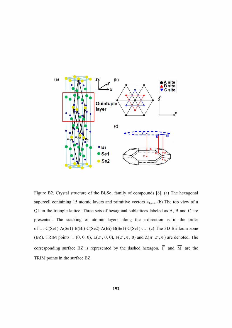
192
Figure B2. Crystal structure of the Bi2Se3 family of compounds [8]. (a) The hexagonal
supercell containing 15 atomic layers and primitive vectors a1,2,3. (b) The top view of a
QL in the triangle lattice. Three sets of hexagonal sublattices labeled as A, B and C are
presented. The stacking of atomic layers along the z-direction is in the order
of …-C(Se1)-A(Se1)-B(Bi)-C(Se2)-A(Bi)-B(Se1)-C(Se1)-…. (c) The 3D Brillouin zone
(BZ). TRIM points (0, 0, 0), L( , 0, 0), F( , , 0) and Z( , , ) are denoted. The
corresponding surface BZ is represented by the dashed hexagon. and M are the
TRIM points in the surface BZ.

193
Figure C1. (a) Bulk band structure of Ag. (b) Band structure of a 20 ML Ag film.
MM ' K
0
-2
-4
-6
-8
2
4
6
8
∥k
(a)
(b)

194
Figure C2. Plane-averaged charge densities of Ag(111) surface states at zone center .
Charge Den
sity (arb. units)
Vac Vac # atomic layer

195
Figure C3. Plane-averaged charge densities in a 20 ML Ag(111) film for (a) quantum well
bulk states and (b) excited states at zone center .
Charge Den
sity (arb. units)
Vac Vac# atomic layer Vac Vac # atomic layer
QWS Excited states
Energy
high
low
(a) (b)

196
Figure D1. (a) Lattice structure of graphene. The lattice constant a=0.246 nm. (b) 2D
Brillouin zone of graphene and projected 1D Brillouin zone of zigzag graphene ribbon. (c)
Band structure of graphene.
xk
yk
1a2a
MK
0
-10
-15
-20
-5
5K
(a) (b)
(c)
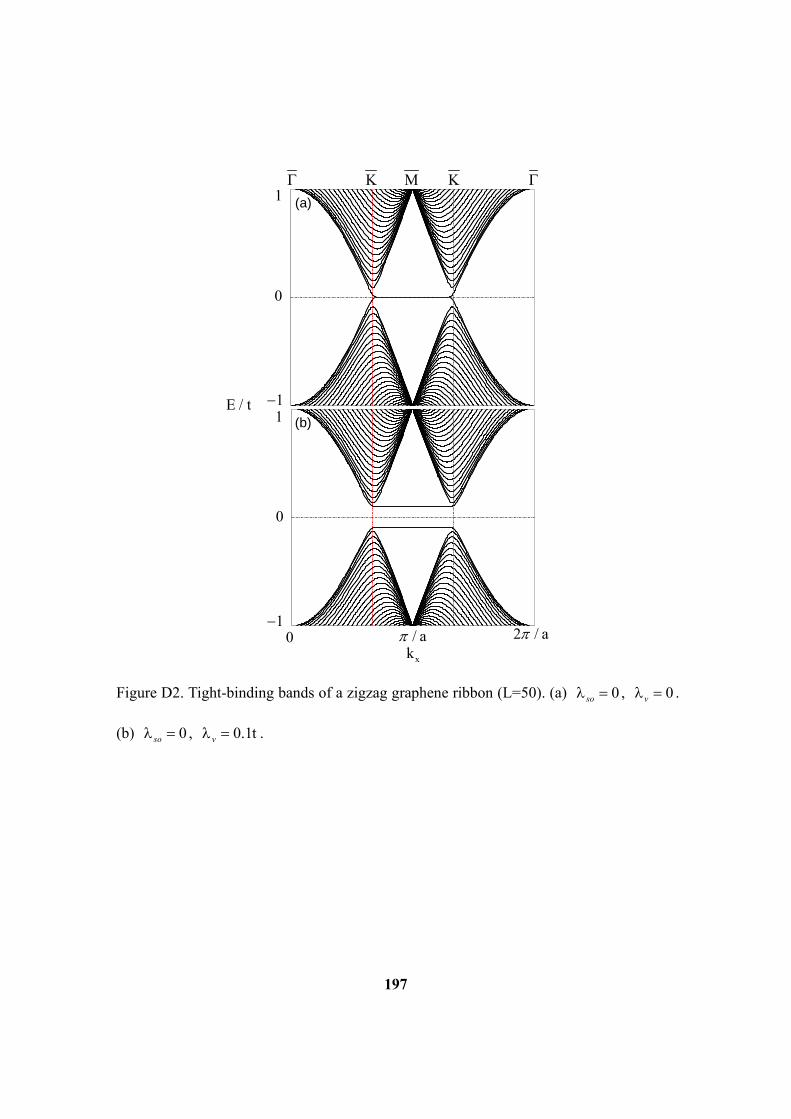
197
Figure D2. Tight-binding bands of a zigzag graphene ribbon (L=50). (a) 0so , 0v .
(b) 0so , 0.1tv .
K M K
E / t
1
0
11
0
1
xk0 / a 2 / a
(a)
(b)

198
Figure D3. Tight-binding bands of a zigzag graphene ribbon (L=50). (a) 0.02tso ,
0.1tv . (b) 3t / 45so , 0.1tv . (c) 0.12tso , 0.1tv . (d) 0.12tso ,
0v .
K M K
E / t
1
0
11
0
1
xk0 / a 2 / a 0 / a 2 / a
K M K (a) (b)
(c) (d)

199
Figure D4. Phase diagram of the Kane-Mele model with SOC ( so ) and a staggered
sublattice potential ( v ).
QSH insulator
Ordinary insulator
v
2
3 3so
v
so
Gap closes
Topological phase transition

200
Figure D5. (a) Schematic of edge potential bias on the top atom chain of a zigzag
graphene ribbon. (b) Tight binding bands of a zigzag graphene ribbon (L=50) with
0.12tso , 0v . The four panels (from left to right) correspond to the edge potential
bias V=0, 0.4t, 1.6t and 400t.
(a)
(b)
E / t
3
0
3
xk0 / a 2 / a 0 / a 2 / a0 / a 2 / a0 / a 2 / a

201
Figure E1. (a) Experimental geometry. (b) Brillouin zone of graphene. (c) ARPES spectra
from graphene near the K point along using 30 eV LCP and RCP photons. (d) Sublattices
of graphene.
(c)
(a) (b)
(c) (d)
x
y

202
Figure E2. ARPES data from monolayer graphene taken with HP, VP, LCP, and RCP
using 30 eV photons. The Dirac point is at -0.45 eV. (a) Constant energy maps at -0.05 eV.
(b) Constant energy maps at -0.9 eV.

203
Figure E3. Simulated constant energy maps below the Dirac point with x y .
0,A HP
8A
3,
4A RCP
3
8A
,2A VP
5
8A
,4A LCP
7
8A
A2φ

204
Figure E4. Simulated constant energy maps below the Dirac point with x yi .
0,A HP
8A
3,
4A LCP
3
8A
,2A VP
5
8A
,4A LCP
7
8A
A2φ

205
Author’s Biography
Guang Bian was born on Feb 18, 1982 in Chifeng, Inner Mongolia, in the northern
region of China. In 2000, he enrolled at Tsinghua University (Beijing) through the
National College Entrance Examination. He graduated magna cum laude with a B.S. in
2004 and a M.S. in 2007. He enrolled at the University of Illinois at Urbana-Champaign
in 2007 and received his Ph.D. in 2012. He was awarded the Best Poster Prize (2009) and
the Aladdin Lamp Award (2010) at the Synchrotron Radiation Center in Stoughton,
Wisconsin. He also received the Yee Memorial Fund Fellowship (2011) and the
University Fellowship (2012) at University of Illinois at Urbana-Champaign.
Publications
1. Guang Bian, Xiaoxiong Wang, T. Miller, and T.-C. Chiang
EuroPhys. Lett. 101, 27004 (2013), “Topological Phase Transition and Dirac Fermion Transfer in
Bi2Se3 Films”.
2. Xiaoxiong Wang, Guang Bian, T. Miller, and T.-C. Chiang
Phys. Rev. B 87, 035109 (2013), “Topological Spin-Polarized Electron Layer above the Surface
of Ca-terminated Bi2Se3”.
3. P. J. Powel, O. Mahapatra, S. A. Brown, Guang Bian, X. Wang, and T.-C. Chiang
Nano lett. 13, 43 (2013), “Electronic Size Effects in Three-Dimensional Nanostructures”.
4. Guang Bian, Xiaoxiong Wang, Yang Liu, T. Miller, and T.-C. Chiang
Phys. Rev. Lett. 108, 176401 (2012), “Interfacial Protection of Topological Surface States in
Ultrathin Sb Films”.
5. Yang Liu, Guang Bian, Thomas Miller, Mark Bissen, and Tai-Chang Chiang
Phys. Rev. B 85, 195442 (2012), “Topological Limit of Ultrathin Quasi-freestanding Bi2Te3 Films
Grown on Si(111)”.
6. Guang Bian, Longxiang Zhang, Yang Liu, Thomas Miller, and Tai-Chang Chiang

206
Phys. Rev. Lett. 108, 186403 (2012), “Detecting Spin Texture of Bi/Ag Surface Alloy by Circular
Angular Resolved Photoemission Spectroscopy”.
7. Xiaoxiong Wang, Guang Bian, T. Miller, and T.-C. Chiang
Phys. Rev. Lett. 108, 096404 (2012), “Fragility of Topological Surface States and Robustness of
Topological Order in Bi2Se3 against Oxidation”.
8. Guang Bian, Xiaoxiong Wang, Yang Liu, T. Miller, and T.-C. Chiang
Phys. Rev. B 84, 235414 (2011), “Symmetry-Constrained Reorganization of Dirac Cones in
Topological Insulators by Surface Modification”.
9. Yang Liu, Guang Bian, Thomas Miller, and Tai-Chang Chiang
Phys. Rev. Lett. 107, 166803 (2011), “Visualizing Electronic Chirality and Berry Phases in
Graphene Systems Using Photoemission with Circularly Polarized Light”. This article is chosen
as a PRL Editors' Suggestion, and is highlighted in a viewpoint article: Thomas Pichler,
"Unraveling electron chirality in graphene", Physics 4, 79 (2011).
10. Guang Bian, Thomas Miller, and Tai-Chang Chiang
Phys. Rev. Lett. 107, 036802 (2011), “Passage from spin-polarized surface states to unpolarized
quantum well states in topologically nontrivial Sb films”. Cover image of Phys. Rev. Lett. Vol.
107, Issue 3 (2011).
11. Yang Liu, Longxiang Zhang, Matthew Brinkley, Guang Bian, Thomas Miller, and Tai-Chang
Chiang
Phys. Rev. Lett. 105, 136804 (2010), “Phonon-induced gaps in graphite/graphene Observed by
angle-resolved photoemission”.
12. Guang Bian, Thomas Miller, and Tai-Chang Chiang
Phys. Rev. B 80, 245407 (2009), “Electronic structure and surface mediated metastability of Bi
films on Si(111)-7×7 studied by angle resolved photoemission spectroscopy”.
13. Guang Bian, Mike Bisset, Nicholas Kersting, Y. Liu, and X. Wang
Eur. Phys. J. C 53 3 429 (2008), “Wedgebox analysis of four-lepton events from neutralino pair
production at the LHC”.

207
14. Lianyi He, Guang Bian, Jinfeng Liao, Pengfei Zhuang
arXiv:hep-ph/0305182 (2003), “Quark Probability Distribution at Finite Temperature and
Density”.