Analysis and Implementation of Coupled Diode...
39
1 IEEE IEEE 802.3 802.3 DTE Power via MDI DTE Power via MDI Analysis and Implementation of Coupled Diode Detection Analysis and Implementation of Coupled Diode Detection Presented by PowerDsine: Amir Lehr - [email protected] Yair Darshan - [email protected] Avinoam Levy - [email protected] Ilan Atias - [email protected] David Pincu - [email protected] Ronen Heldman - [email protected]
Transcript of Analysis and Implementation of Coupled Diode...
1
IEEE IEEE 802.3802.3 DTE Power via MDI DTE Power via MDIAnalysis and Implementation of Coupled Diode DetectionAnalysis and Implementation of Coupled Diode Detection
Presented by PowerDsine:Amir Lehr - [email protected] Darshan - [email protected] Levy - [email protected] Atias - [email protected] Pincu - [email protected] Heldman - [email protected]

2Analysis of Coupled Diode Detection, Yair Darshan, PowerDsine, Rev-001
IEEE 802.3af, Sep. 2000.
Coupled Diode MethodDefining parameters for cost-effective implementation
! PD Section! Isolating Circuit
! PSE (Switch, Mid-Span)! Probing signal feeding methods with coupling transformer! Two transformers implementation! Single transformer implementation! Silicon implementation
Acknowledgment to Rick Brooks & Larry Miller / Nortel Their previous work is used as the baseline for this presentation
3Analysis of Coupled Diode Detection, Yair Darshan, PowerDsine, Rev-001
IEEE 802.3af, Sep. 2000.
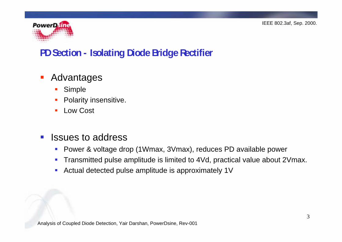
PD Section - Isolating Diode Bridge Rectifier
! Advantages! Simple! Polarity insensitive.! Low Cost
! Issues to address! Power & voltage drop (1Wmax, 3Vmax), reduces PD available power ! Transmitted pulse amplitude is limited to 4Vd, practical value about 2Vmax.! Actual detected pulse amplitude is approximately 1V

4Analysis of Coupled Diode Detection, Yair Darshan, PowerDsine, Rev-001
IEEE 802.3af, Sep. 2000.
PD section- Enhanced Isolating Circuit
! Reliable implementation must include an Under Voltage protection circuit as part of the PD power supply input*
! The UV circuitry may be utilized as the isolation block between the Coupled Diode signature element and the PD power supply
* Refer to the PowerDsine IEEE 802.3af May 2000 presentation

5Analysis of Coupled Diode Detection, Yair Darshan, PowerDsine, Rev-001
IEEE 802.3af, Sep. 2000.
PD Section - Isolation Circuitry
DC/DC Converter
C1470uF
R1
2K
R3100K
C21uF
D4D1N4148
D7D1N4002
D2
D1N4002
D1D1N4002
D6D1N4002
D5D1N4002
D3D1N4002
R2+
-
Coupled Diode
(-)
(+)
IsolatingCircuit

6Analysis of Coupled Diode Detection, Yair Darshan, PowerDsine, Rev-001
IEEE 802.3af, Sep. 2000.
PD Section - Enhanced Isolation Circuitry
* Hysteresis circuitry may be added for setting different On/Off thresholds
DC/DC Converter
D4
R110.5K-0805
R546.4K-0805
M1IRLW530A
C2470uF
C11uF
R4100K
R2
2K
D1
D1N4148
D5D1N4002
D3
DIODE
D2
C31uF
R3
Z=12V
VZ=33V
-
+
(+)
(-)
Isolator & UnderVoltage Lock Out
Coupled DiodeCircuit
7Analysis of Coupled Diode Detection, Yair Darshan, PowerDsine, Rev-001
IEEE 802.3af, Sep. 2000.
PD section - Enhanced Isolating Circuitry
! Utilizing the existing UVLO
! Increases PD available power by reducing diodes power/voltage drop
! Probing pulses amplitude value range can be widen to improve signal to noise ratio and lower detected pulse sensitivity to circuit elements tolerance
! Lab testing confirms that the detected pulse shape is highly similar to one measured using the Diode Bridge

8Analysis of Coupled Diode Detection, Yair Darshan, PowerDsine, Rev-001
IEEE 802.3af, Sep. 2000.
PSE - Pulse Amplitude Limitations
Setup A
Nortel proposed setup
! Mid-Span solution architecture
Setup B
Power is Phantom fed through standard data transformer module including integrated data path common mode filter
! Switch solution architecture
! Common mode filter inductance may vary in range of 2-120uH (depends on application, vendors etc.)
0
0
..
Dataout
.
.PSE
Dataout
+
DTE
Coupleddiodecircuit
.
Isolatorcircuit
.
.
Data in
.
.
Data in
.
Load
.
probingsignalIN2/OUT1
probingsignalIN1/OUT2
.
..
..
0
0
..
..
..
..
+
..
. .
Coupleddiodecircuit
Isolatorcircuit Load
probingsignalIN1/OUT2
probingsignalIN2/OUT1
DTEPSE

9Analysis of Coupled Diode Detection, Yair Darshan, PowerDsine, Rev-001
IEEE 802.3af, Sep. 2000.
Detected Pulse Shape Vs. Link Length
Setup A: Link length=0-100m, 5m steps Ti me
4. 9000ms 4. 9050ms 4. 9100ms 4. 9150ms4. 8954ms 4. 9193msV( C11: 2)
- 1. 00V
0V
1. 00V
1. 58V

10Analysis of Coupled Diode Detection, Yair Darshan, PowerDsine, Rev-001
IEEE 802.3af, Sep. 2000.
Detected Pulse Shape vs. Link Length
Ti me
4 . 9000ms 4 . 9050ms 4 . 9100ms 4 . 9150ms4 . 8957ms 4 . 9193msV( R9: 2)
- 0 . 50V
0V
0. 50V
1. 00V
1. 28V
Setup B: Link length = 100m, 0-100uH Common Mode inductance, 5uH steps
Refer to Annex C for details

11Analysis of Coupled Diode Detection, Yair Darshan, PowerDsine, Rev-001
IEEE 802.3af, Sep. 2000.
Recommendations
Setup A: ! Detected signal shape changes within acceptable detected and processed
range
Setup B:! Pulse leading edge changes significantly with series inductance! Pulse sampling time should be positioned close to tailing edge for robust
detection
Note! While power over MDI is supplied the Common Mode filter inductance that is
located inside the link will be significantly reduced due to core saturation. This may affect common mode noise rejection. Consider locating Common Mode filter external to the link side

12Analysis of Coupled Diode Detection, Yair Darshan, PowerDsine, Rev-001
IEEE 802.3af, Sep. 2000.
PSE Detection Circuitry Implementations
! Proposed coupled diode concept requires two coupling transformers
! Questions! Can we reduce it to single transformer?! Can we find solutions that can fit on Silicon?
! Goal: ! Specifying pulse shape parameters which do not limit the implementation
methods

13Analysis of Coupled Diode Detection, Yair Darshan, PowerDsine, Rev-001
IEEE 802.3af, Sep. 2000.Two Transformers Circuitry Can We Reduce it to a single Coupling Transformer?
Limits max. probing signal pulse width
Limits min. probing signal pulse width
Drive_Trafo
Drive_Trafo
IN1
IN2
OUT1
OUT2
Drive_Trafo0
Drive_Trafo
IN1
IN2
OUT1
OUT2
TX_Data_trafo
TX_Data_trafo
TDP
TDCT
TDN
TXP
TXN
TXCT
RX_Data_trafo
RX_Data_trafo
RXN
RXCT
RXP
RDN
RDP
RDCT
RX_Data_trafo0
RX_Data_trafo
RXN
RXCT
RXP
RDN
RDP
RDCT
TX_Data_trafo0
TX_Data_trafo
TDP
TDCT
TDN
TXP
TXN
TXCT
0
0
0
0
0
0
0
bbb
Chassis
Chassis
Chassis
DTE_N
DTE_N
DTE_P
DTE_N
aaa
R25{R_Line*Length}
21
C10
{0.5*C_Line*Length}
D1
D1N4148
C30.01u
R26{R_Line*Length}
21
R9100
R27{R_Line*Length}
21
R28{R_Line*Length}
21
V3
0V
R2310MEG
D2
D1N4148
R250
R750
R1450
R1950
C41U
R102k
R11100k
L66{L_Line*Length}
C210n
V1
C610n
R410meg
R1610meg
V2
D9
D1N4002
D8
D1N4002
D7
D1N4002
D6
D1N4002
D5
D1N4002
D4
D1N4002
R310meg
R610meg
R1510meg
R1810meg
R2410MEG
C9220uF
R29117
R8{Rdrive}
R21
{Rdrive}
R3010MEG
C112.7n
R13
0.001
R32
0.1
C122.7nF
L1
100uH
C5220U
R12
1k
R310.2
R5100
L65{L_Line*Length}
PARAMETERS:
k_data = 0.998
L_cm = 100u
Rdrive = 12Vdrive = 3.3
L_Drive = 1.2mHN_Drive = 1
Length = 100
L_data = 350u
K_Drive = 0.9997
L_data1 = 350u
C_Line = 15pFL_Line = 0.3uHR_Line = 0.125
R17100
L67{L_Line*Length}
L68{L_Line*Length}
C80.01u
D3
D1N4148
R22100
C13{0.5*C_Line*Length}
R2075
C71n
R175
C11n
/m (Scaled)/m (Scaled)/m (Scaled)
m
14Analysis of Coupled Diode Detection, Yair Darshan, PowerDsine, Rev-001
IEEE 802.3af, Sep. 2000.
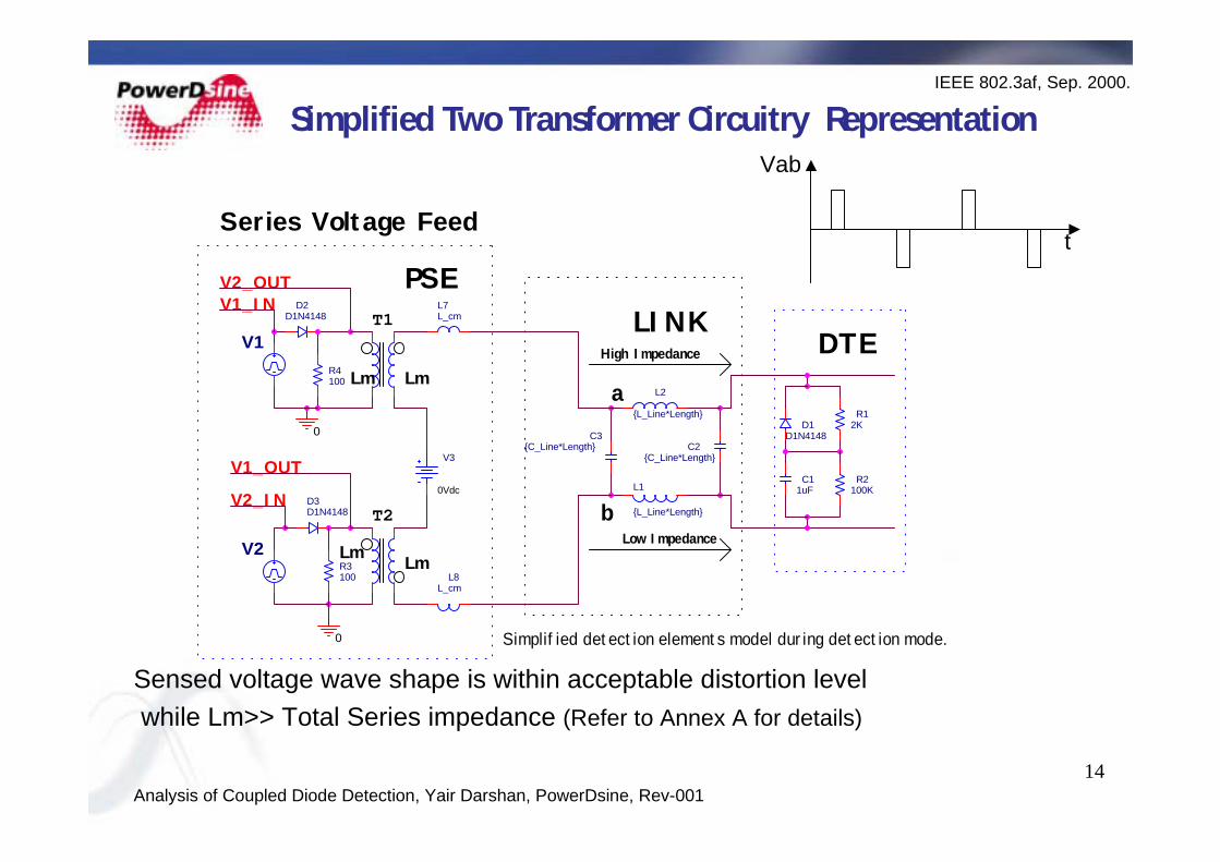
Simplified Two Transformer Circuitry Representation
Sensed voltage wave shape is within acceptable distortion level while Lm>> Total Series impedance (Refer to Annex A for details)
Vab
t
0
0
V2_OUTV1_IN
V2_IN
V1_OUTV3
0Vdc
C2{C_Line*Length}
L1
{L_Line*Length}
L2
{L_Line*Length}
C3{C_Line*Length}
C11uF
R2100K
R12KD1
D1N4148
V1
D2D1N4148
R4100
D3D1N4148
R3100
V2
L7L_cm
L8L_cm
Series Voltage Feed
Lm Lm
LmLm
a
bLow Impedance
PSE
DTELINK
High Impedance
T1
T2
Simplified detection elements model during detection mode.

15Analysis of Coupled Diode Detection, Yair Darshan, PowerDsine, Rev-001
IEEE 802.3af, Sep. 2000.Two Transformer Circuit - Test Results Setup A & B measurements,100m Cat 5 UTP cable
Diode non-conducting direction Diode conducting direction
Shorted load Open load
16Analysis of Coupled Diode Detection, Yair Darshan, PowerDsine, Rev-001
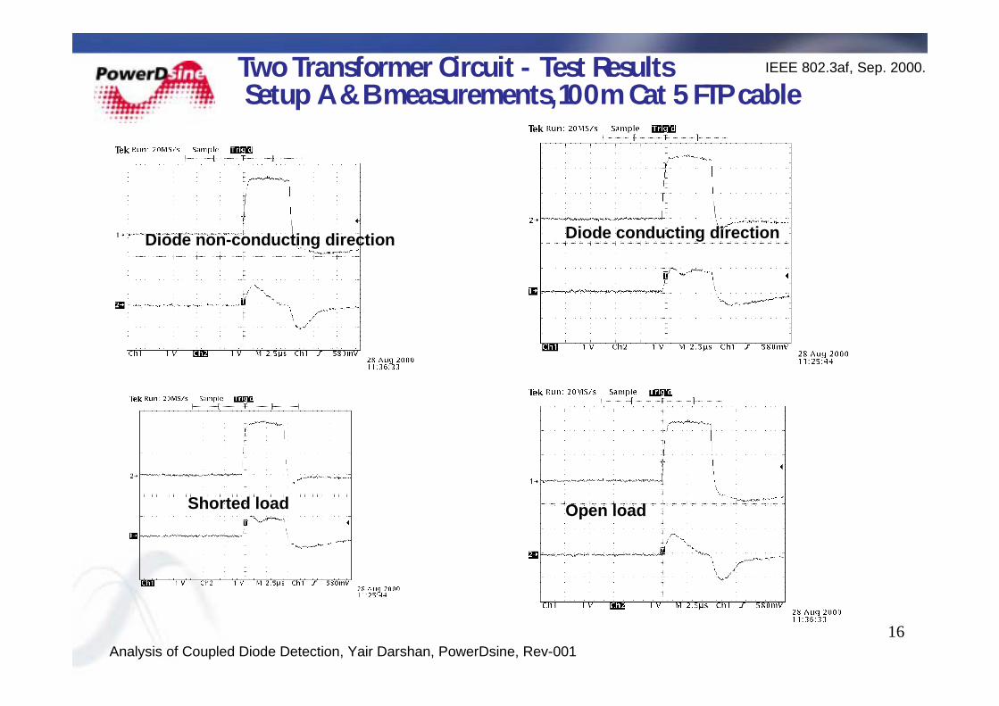
IEEE 802.3af, Sep. 2000.Two Transformer Circuit - Test Results Setup A & B measurements,100m Cat 5 FTP cable
Diode non-conducting direction Diode conducting direction
Shorted load Open load

17Analysis of Coupled Diode Detection, Yair Darshan, PowerDsine, Rev-001
IEEE 802.3af, Sep. 2000.Two Transformer Circuit - Test Results Setup A & B measurements,0.2m Cat 5 FTP/UTP cable
Diode non-conducting direction Diode conducting direction

18Analysis of Coupled Diode Detection, Yair Darshan, PowerDsine, Rev-001
IEEE 802.3af, Sep. 2000.
Two Transformer Circuit - Test Results
! Measured results confirm those presented by Rick Brooks & Larry Miller / Nortel at the July 2000 meeting
! The detected signal is affected by the Cat 5 cable equivalent input capacitance between pairs (by-passing Coupled Diode Signature element)
! Simple High Pass filter at receive side can improve performance

19Analysis of Coupled Diode Detection, Yair Darshan, PowerDsine, Rev-001
IEEE 802.3af, Sep. 2000.
Reduction to Single Transformer Circuit
Limits min. probing signal pulse width
Limits max. probing signal pulse width
Drive_Trafo0
Drive_Trafo
IN1
IN2
OUT1
OUT2
RX_Data_trafo2
RX_Data_trafo
RXN
RXCT
RXP
RDN
RDP
RDCT
TX_Data_trafo1
TX_Data_trafo
TDP
TDCT
TDN
TXP
TXN
TXCT
RX_Data_trafo1
RX_Data_trafo
RXN
RXCT
RXP
RDN
RDP
RDCT
TX_Data_trafo2
TX_Data_trafo
TDP
TDCT
TDN
TXP
TXN
TXCT
0
0
0
0
0
0
0
0
bbb
Chassis
Chassis
Chassis
DTE_N
DTE_P
DTE_N
aaa
DTE_N
V2_IN_V1_OUT
V1_IN_V2_OUT
C10
{0.5*C_Line*Length}
L66{L_Line*Length}
C1122nF
V2
R21{Rdrive}
R8{Rdrive}
R32
0.1
C1222nF
R25{R_Line*Length}
21
R26{R_Line*Length}
21
R27{R_Line*Length}
21
R28{R_Line*Length}
21
V3
0V
R2310MEG
D2
D1N4148
R250
R750
R1450
R1950
R102k
C41UR11
100k
C210n
C610n
R410meg
R1610meg
V1
D9
D1N4002
D8
D1N4002D7
D1N4002
R310meg
D6
D1N4002
D5
D1N4002
D4
D1N4002
R610meg
R1510meg
R1810meg
R2410MEG
C9220uF
R29117
R3010MEG
L1
100uH
R13
0.001
C5220U
R12
1k
R5100
PARAMETERS:
k_data = 0.998
L_cm = 100U
Rdrive = 100Vdrive = 2
L_Drive = 5mHN_Drive = 1
Length = 100
L_data = 350u
K_Drive = 0.9997
L_data1 = 350u
C_Line = 15pL_Line = 0.3uHR_Line = 0.125
R17100
R2075
C71n
R175
C11n
D3
D1N4148
R310.2
L65{L_Line*Length}
L67{L_Line*Length}
L68{L_Line*Length}
C13{0.5*C_Line*Length}
D11
D1N4148
/m (Scaled)/m (Scaled)/m
m

20Analysis of Coupled Diode Detection, Yair Darshan, PowerDsine, Rev-001
IEEE 802.3af, Sep. 2000.
Simplified Single Transformer Circuit Model
Sensed voltage wave shape is within acceptable distortion level while Im << Ishort(Refer to Annex B for details)
Vab
t
0
V2_OUT
V1_OUTV2 R5100
V1 R4100
V3
0Vdc
C2{C_Line*Length}
L1
{L_Line*Length}
L2
{L_Line*Length}
C3{C_Line*Length}
D1D1N4148
R12K
R2100K
C11UF
L7L_cm
Series Voltage Feed ,Current Sense.
Lma
bLow Impedance
PSE
DTELINK
High Impedance
Lm
T1
Simplified detection elements model during detection mode.

21Analysis of Coupled Diode Detection, Yair Darshan, PowerDsine, Rev-001
IEEE 802.3af, Sep. 2000.
Single Transformer Circuit - Concept Principles
! Coupling transformer primary inputs are driven with two low impedance pulse source introducing 180 degree phase shift.
! Sensing Primary current for short / open condition (Coupled diode is conducting or reversed biased)
! Primary winding is always closed circuit to ground.! Clean and noise-free pulse shape at secondary.
! Pulse parameters requirements are compatible with 2 transformer solution

22Analysis of Coupled Diode Detection, Yair Darshan, PowerDsine, Rev-001
IEEE 802.3af, Sep. 2000.
Single Transformer Circuit - Simulation! Setup: 100m Cat 5 UTP cable! Cable parameters measured between pairs 4/5 to 7/8 and 1/2 to 3/6
V1_IN V2_OUT
V1_OUT V2_IN Ti me
4. 70ms 4. 75ms 4. 80ms 4. 85ms 4. 90ms 4. 95ms 5. 00msV( V2_I N_V1_OUT)
- 4 . 0V
0V
4. 0V
SEL>>
V( V1_I N_V2_OUT)- 4 . 0V
0V
4. 0V

23Analysis of Coupled Diode Detection, Yair Darshan, PowerDsine, Rev-001
IEEE 802.3af, Sep. 2000.Single Transformer Circuit - MeasurementsSetup A & B, 100m Cat 5, UTP cable
Diode non-conducting direction Diode conducting direction
Shorted load Open load

24Analysis of Coupled Diode Detection, Yair Darshan, PowerDsine, Rev-001
IEEE 802.3af, Sep. 2000.Single Transformer Circuit - MeasurementsSetup: Mid-Span,100m Cat 5 FTP cable
Diode non-conducting direction Diode conducting direction
Shorted load Open load

25Analysis of Coupled Diode Detection, Yair Darshan, PowerDsine, Rev-001
IEEE 802.3af, Sep. 2000.Single Transformer Circuit - MeasurementsSetup: Mid-Span, 20cm Cat 5 UTP cable
Diode non-conducting direction Diode conducting direction
Shorted load Open load
26Analysis of Coupled Diode Detection, Yair Darshan, PowerDsine, Rev-001
IEEE 802.3af, Sep. 2000.
Single Transformer Circuit - Conclusions
! Utilizing a single coupling transformer is feasible
! Similar results were observed for both A and B setup

27Analysis of Coupled Diode Detection, Yair Darshan, PowerDsine, Rev-001
IEEE 802.3af, Sep. 2000.
Comparison Between Single / Double Transformers
*Further investigation and testing should be performed to evaluate impact on cost and footprint
Probing signal sensing methodParameter Single Transformer Double TransformerMin. Primary inductance 4mH 1.350mHOperating mode Voltage pulse transformer Voltage pulse transformerFootprint about 0.6X 1" x 0.5" = XCost TBD TBD

28Analysis of Coupled Diode Detection, Yair Darshan, PowerDsine, Rev-001
IEEE 802.3af, Sep. 2000.
Coupled Diode Implementation Limitations
! Series voltage pulses feeding requires coupling transformers
! Implementing this scheme without using coupling transformers must utilize a different type of probing pulse feeding method
! Parallel voltage pulse feeding is required to allow future Silicon implementation

29Analysis of Coupled Diode Detection, Yair Darshan, PowerDsine, Rev-001
IEEE 802.3af, Sep. 2000.
RX_Data_trafo2
RX_Data_trafo
RXN
RXCT
RXP
RDN
RDP
RDCT
TX_Data_trafo1
TX_Data_trafo
TDP
TDCT
TDN
TXP
TXN
TXCT
RX_Data_trafo1
RX_Data_trafo
RXN
RXCT
RXP
RDN
RDP
RDCT
TX_Data_trafo2
TX_Data_trafo
TDP
TDCT
TDN
TXP
TXN
TXCT
0
0
0
0
0
0
Chassis
Chassis
Chassis
DTE_N
DTE_P
DTE_N
DTE_N
VP1 V_PORT
VP2
C10
{0.5*C_Line*Length}
L66{L_Line*Length}
V2
D3D1N4002
R32
0.1
R25{R_Line*Length}
21
R26{R_Line*Length}
21
R27{R_Line*Length}
21
R28{R_Line*Length}
21
V30V
R2310MEG
D1
D1N4148
R1150
R750
R1450
R1950
R12k
C11UR2
100k
C210n
C610n
R410meg
R1610meg
V1
D9
D1N4002
D8
D1N4002D7
D1N4002
R310meg
D6
D1N4002
D5
D1N4002
D4
D1N4002
R610meg
R1510meg
R1810meg
R2410MEG
C9220uF
R29117
R3010MEG
R5100
C50.47uF
R17100
PARAMETERS:
k_data = 0.998
L_cm = 5u
Rdrive = 100Vdrive = 2
Length = 100
L_data = 350uL_data1 = 350u
C_Line = 15pL_Line = 0.3uHR_Line = 0.125
T_rise = 10uT_fall = 10uT_per = 8msT_delay = 6msT_ch = 5msT_dch = 100u
R2075
C71n
R1075
C41n
R12100
R310.2
L65{L_Line*Length}
L67{L_Line*Length}
L68{L_Line*Length}
C13{0.5*C_Line*Length}
D2D1N4148
M5
2N7000
R9
10
/m (Scaled)/m (Scaled)/mm
Transformer-less Implementation
Limits minimum pulse width
Switch, Current limit protection etc.
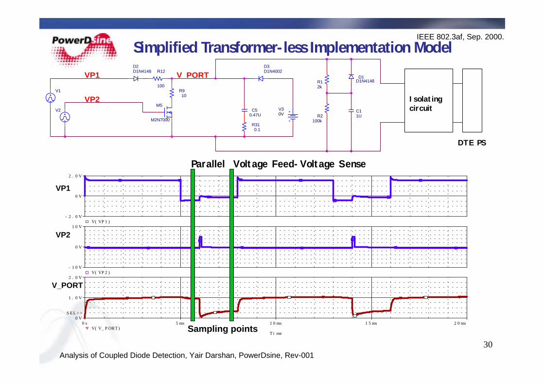
30Analysis of Coupled Diode Detection, Yair Darshan, PowerDsine, Rev-001
IEEE 802.3af, Sep. 2000.Simplified Transformer-less Implementation Model
T i me
0 s 5 ms 1 0 ms 1 5 ms 2 0 msV( V_ P ORT )
0 V
1 . 0 V
2 . 0 V
S E L > >
V( VP 2 )- 1 0 V
0 V
1 0 VV( VP 1 )
- 2 . 0 V
0 V
2 . 0 V
Sampling points
VP1
VP2
V_PORT
VP1
VP2
V_PORT
V2
D3D1N4002
D1D1N4148
V30V R2
100k
C11U
R12k
V1
C50.47U
R12
100
R310.1
R910
M5
M2N7000
D2D1N4148
Isolatingcircuit
DTE PS
Parallel Voltage Feed-Voltage Sense

31
Transformer-less Implementation - Waveforms
dT1 dT2 dT3 dT4 dT1 dT1: Diode is at non-conduction direction, Cap is charged to V1.dT2: Port output pulse voltage peak is sensed for V1±TBD% within dT2 gape.dT3: Diode is in conducting direction, by shorting the port for limited time dT3.dT4: Port output pulse voltage valley is sensed for V2=0.7V ±TBD% within dT4 gape.!All other digital pulse manipulation and processing apply to this concept as well and are conceptually similar to Series Feed solutions (with the transformers…)
Ti me
0 s 2 ms 4 ms 6 ms 8 ms 1 0 ms 1 1 msV( V_ P ORT)
0 V
1 . 0 V
2 . 0 V
S EL> >
V( VP 2 )- 1 0 V
0 V
1 0 VV( VP 1 )
- 2 . 0 V
0 V
2 . 0 VVP1
VP2
V_PORT
V1V2

32Analysis of Coupled Diode Detection, Yair Darshan, PowerDsine, Rev-001
IEEE 802.3af, Sep. 2000.
Transformer-less solution - Concept Principles
! Parallel probing signal feeding method
! AC coupled diode elements are detected by two pulse sources with different characteristics.
! Detected signal is unique function of coupled diode elements values.
! Immunity to ambiguous detection is ensured by pseudo randomly changing pulse width on both pulse sources.! In addition to behavioral signature detection, higher level of
detection reliability can be achieved by utilizing the forward and reversed AC coupled diode time constant network.
33Analysis of Coupled Diode Detection, Yair Darshan, PowerDsine, Rev-001
IEEE 802.3af, Sep. 2000.
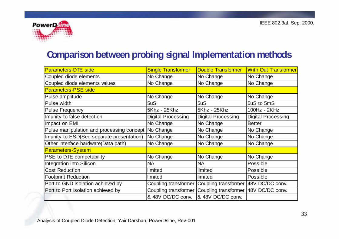
Comparison between probing signal Implementation methods
Parameters-DTE side Single Transformer Double Transformer With Out TransformerCoupled diode elements No Change No Change No ChangeCoupled diode elements values No Change No Change No ChangeParameters-PSE sidePulse amplitude No Change No Change No ChangePulse width 5uS 5uS 5uS to 5mSPulse Frequency 5Khz - 25Khz 5Khz - 25Khz 100Hz - 2KHzImunity to false detection Digital Processing Digital Processing Digital ProcessingImpact on EMI No Change No Change BetterPulse manipulation and processing concept No Change No Change No ChangeImunity to ESD(See separate presentation) No Change No Change No ChangeOther Interface hardware(Data path) No Change No Change No ChangeParameters-SystemPSE to DTE competability No Change No Change No ChangeIntegration into Silicon NA NA PossibleCost Reduction limited limited PossibleFootprint Reduction limited limited PossiblePort to GND isolation achieved by Coupling transformer Coupling transformer 48V DC/DC conv.Port to Port Isolation achieved by Coupling transformer Coupling transformer 48V DC/DC conv.
& 48V DC/DC conv. & 48V DC/DC conv.

34Analysis of Coupled Diode Detection, Yair Darshan, PowerDsine, Rev-001
IEEE 802.3af, Sep. 2000.
Implication on Detection Parameters Specifications
! Same coupled diode signature circuit is used in all probing signal feeding methods
! Proposed coupled diode and pulse parameters specifications should not limit implementation methods
! Transformers and silicon implementations will be feasible if a wider range of parameters be specified:! Frequency ( 5Khz to 25Khz and 100Hz to 2Khz)
! Pulse width (5uS, 5uS to 5ms)
! Pulse Amplitude TBD
! Pulse average power (TBD mW max.)
! Successful detection if TBDmin to 256max consecutive positive detection cycles where received.
35Analysis of Coupled Diode Detection, Yair Darshan, PowerDsine, Rev-001
IEEE 802.3af, Sep. 2000.
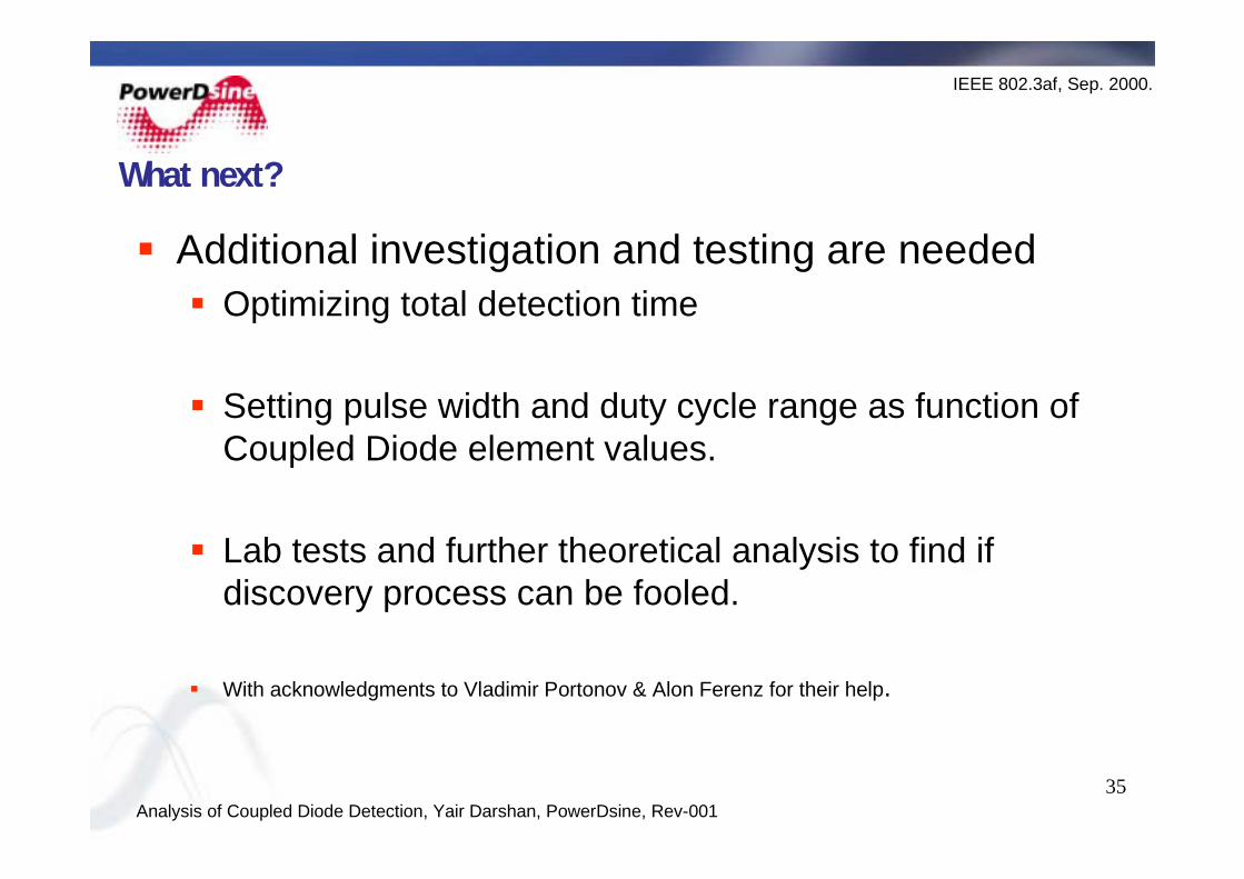
What next?
! Additional investigation and testing are needed! Optimizing total detection time
! Setting pulse width and duty cycle range as function of Coupled Diode element values.
! Lab tests and further theoretical analysis to find if discovery process can be fooled.
! With acknowledgments to Vladimir Portonov & Alon Ferenz for their help.
36Analysis of Coupled Diode Detection, Yair Darshan, PowerDsine, Rev-001
IEEE 802.3af, Sep. 2000.
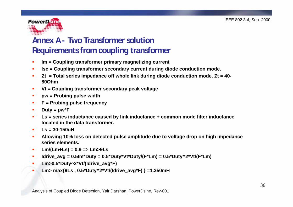
Annex A - Two Transformer solutionRequirements from coupling transformer ! Im = Coupling transformer primary magnetizing current! Isc = Coupling transformer secondary current during diode conduction mode.! Zt = Total series impedance off whole link during diode conduction mode. Zt = 40-
80Ohm! Vt = Coupling transformer secondary peak voltage! pw = Probing pulse width! F = Probing pulse frequency! Duty = pw*F! Ls = series inductance caused by link inductance + common mode filter inductance
located in the data transformer.! Ls = 30-150uH! Allowing 10% loss on detected pulse amplitude due to voltage drop on high impedance
series elements.! Lm/(Lm+Ls) = 0.9 => Lm>9Ls! Idrive_avg = 0.5Im*Duty = 0.5*Duty*Vt*Duty/(F*Lm) = 0.5*Duty^2*Vt/(F*Lm)! Lm>0.5*Duty^2*Vt/(Idrive_avg*F)! Lm> max{9Ls , 0.5*Duty^2*Vt/(Idrive_avg*F) } =1.350mH

37Analysis of Coupled Diode Detection, Yair Darshan, PowerDsine, Rev-001
IEEE 802.3af, Sep. 2000.
Annex B - Single Transformer solutionRequirements From Coupling transformer! Im = Coupling transformer primary magnetizing current! Isc = Coupling transformer secondary current during diode conduction mode.! Zt = Total series impedance off whole link during diode conduction mode. Zt = 40-80Ohm! Vt = Coupling transformer secondary peak voltage! pw = Probing pulse width! F = Probing pulse frequency! Duty = pw*F! Ls = series inductance caused by link inductance + common mode filter inductance located
in the data transformer! For keeping detection resolution within safe margin: Im<Isc / 10! Isc = Vt/Zt = 25mA - 50mA! Lm>Vt/(Im/pw) = 2/(0.1*25mA/5uS)=4mH! Lm>4mH

38Analysis of Coupled Diode Detection, Yair Darshan, PowerDsine, Rev-001
IEEE 802.3af, Sep. 2000.
Annex C - Setup B Electrical Model for Circuit Elements During Detection Mode
Drive_Trafo
Drive_Trafo
IN1
IN2
OUT1
OUT2
Drive_Trafo0
Drive_Trafo
IN1
IN2
OUT1
OUT2
TX_Data_trafo
TX_Data_trafo
TDP
TDCT
TDN
TXP
TXN
TXCT
RX_Data_trafo
RX_Data_trafo
RXN
RXCT
RXP
RDN
RDP
RDCT
RX_Data_trafo0
RX_Data_trafo
RXN
RXCT
RXP
RDN
RDP
RDCT
TX_Data_trafo0
TX_Data_trafo
TDP
TDCT
TDN
TXP
TXN
TXCT
0
0
0
0
0
0
0
bbb
Chassis
Chassis
Chassis
DTE_N
DTE_N
DTE_P
DTE_N
aaa
C30.01u
D1
D1N4148
C10
{0.5*C_Line*Length}
R25{R_Line*Length}
21
R28{R_Line*Length}
21
R27{R_Line*Length}
21
R9100
R26{R_Line*Length}
21
V3
0V
R2310MEG
R1950
R1450
R750
R250
D2
D1N4148
R11100k
R102k
C41U
L66{L_Line*Length}
C210n
V1
C610n
R410meg
R1610meg
V2
D4
D1N4002
D5
D1N4002
D6
D1N4002
D7
D1N4002
D8
D1N4002
D9
D1N4002
R1810meg
R1510meg
R610meg
R310meg
R2410MEG
R29117
C9220uF
R21
{Rdrive}
R8{Rdrive}
R3010MEG
C112.7n
R13
0.001
R32
0.1
C122.7nF
C5220U
L1
100uH
R12
1k
R310.2
R5100
PARAMETERS:
k_data = 0.998
L_cm = 100u
Rdrive = 12Vdrive = 3.3
L_Drive = 1.2mHN_Drive = 1
Length = 100
L_data = 350u
K_Drive = 0.9997
L_data1 = 350u
C_Line = 15pFL_Line = 0.3uHR_Line = 0.125
L65{L_Line*Length}
R17100
L67{L_Line*Length}
L68{L_Line*Length}
C13{0.5*C_Line*Length}
R22100
D3
D1N4148
C80.01u
C71n
R2075
C11n
R175
/m (Scaled)/m (Scaled)/m (Scaled)
m
39Analysis of Coupled Diode Detection, Yair Darshan, PowerDsine, Rev-001
IEEE 802.3af, Sep. 2000.
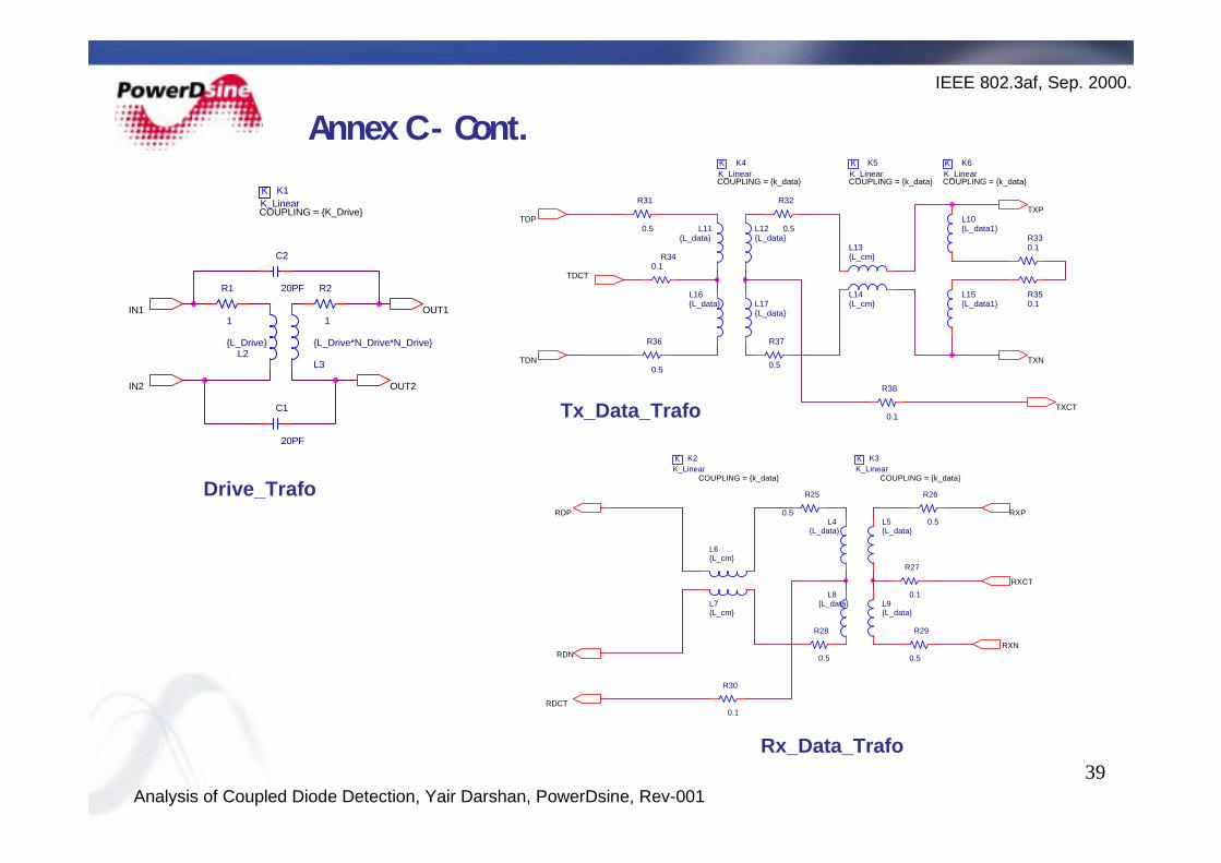
Annex C - Cont.
L11{L_data}
L12{L_data}
K K4
COUPLING = {k_data}K_Linear
L17{L_data}
L16{L_data}
L13{L_cm}
L14{L_cm}
L10{L_data1}
L15{L_data1}
K K5
COUPLING = {k_data}K_Linear
K K6
COUPLING = {k_data}K_Linear
R38
0.1
R340.1
R330.1
R350.1
R31
0.5
R36
0.5
R37
0.5
R32
0.5TDP
TDCT
TDN
TXP
TXN
TXCTTx_Data_Trafo
L8{L_data} L9
{L_data}
L4{L_data}
L5{L_data}
L6{L_cm}
L7{L_cm}
K K2
COUPLING = {k_data}K_Linear
K K3
COUPLING = {k_data}K_Linear
R30
0.1
R27
0.1
R25
0.5
R28
0.5
R29
0.5
R26
0.5
RXN
RXCT
RXP
RDN
RDP
RDCT
Rx_Data_Trafo
L2{L_Drive}
L3
{L_Drive*N_Drive*N_Drive}
K K1
COUPLING = {K_Drive}K_Linear
R1
1
R2
1
C1
20PF
C2
20PF
IN1
IN2
OUT1
OUT2
Drive_Trafo