analog vlsi phototransduction - INI Institute of Neuroinformatics
26
Irradiance (mW/m 2 ) Peak Output (V) 2.4 2.6 2.8 3 3.2 3.4 10 -3 10 -2 10 -1 10 0 10 1 10 2 10 3 10 4 10 5 Transient Responses Steady-state response CALIFORNIA INSTITUTE OF TECHNOLOGY COMPUTATION AND NEURAL SYSTEMS PROGRAM CNS Memo No. 30, April 2, 1996 PASADENA, CALIFORNIA 91125 T. Delbrück & C.A. Mead A NALOG VLSI P HOTOTRANSDUCTION by continuous-time, adaptive, logarithmic photoreceptor circuits Photodiode ( C p ) (also hole in overlying metal) Storage Capacitor (C 1 ) Feedback capacitor (C 2 ) Amplifier Cascode transistor Adaptive element Feedback transistor 6 μm (C o ) V p V o V f C 2 C 1 I bg +i V b Input Model Comparison Learning Q fb Q n Q p Adaptive element V cas Q cas Frequency (Hz) 0 -1 -2 1/ f Instrumentation 1/ f 2 -140 -120 -100 10 -1 10 0 10 1 10 2 10 3 10 4 Signal Amplitude (dBV/√Hz) Log Intensity
Transcript of analog vlsi phototransduction - INI Institute of Neuroinformatics

Irradiance (mW/m2)
PeakOutput
(V)
2.4
2.6
2.8
3
3.2
3.4
10-3
10-2
10-1
100
101
102
103
104
105
TransientResponses
Steady-stateresponse
CALIFORNIA INSTITUTE OF TECHNOLOGYCOMPUTATION AND NEURAL SYSTEMS PROGRAM
CNS Memo No. 30, April 2, 1996
PASADENA, CALIFORNIA 91125
T. Delbrück & C.A. Mead
A
NALOG
VLSI P
HOTOTRANSDUCTION
by continuous-time, adaptive, logarithmic photoreceptor circuits
Photodiode (Cp)
(also hole in overlying metal)
StorageCapacitor(C1)
Feedbackcapacitor(C2)
Amplifier
Cascodetransistor
Adaptiveelement
Feedback transistor
6 µm
(Co)
Vp
Vo
Vf
C2
C1
Ibg+i
Vb
Input
Model
Comparison
Learning
Qfb
Qn
QpAdaptiveelement
VcasQcas
Frequency (Hz)
0
-1
-2
1/f Instrumentation
1/f2
-140
-120
-100
10-1
100
101
102
103
104
Sig
nal A
mp
litud
e (d
BV
/√H
z) Log Intensity

2
4/2/96
Analog VLSI Phototransduction CNS Memo #30 T. Delbrück & C.A. Mead
This paper describes an adaptive photorecep-tor circuit that can be used in massively paral-lel analog VLSI silicon chips. The receptorprovides a continuous-time output that haslow gain for static signals (including circuitmismatches), and high gain for transient sig-nals that are centered around the adaptationpoint. The response is logarithmic with illu-mination, which makes the response to afixed image contrast invariant to absolutelight intensity.
The 5-transistor receptor can be fabricatedin an area of about 70 by 70
µ
m
2
in a 2-
µ
msingle-poly CMOS technology. It has adynamic range of 1–2 decades at a singleadaptation level, and a total dynamic range ofmore than 6 decades. Several technicalimprovements in the circuit yield an addi-tional 1–2 decades dynamic range over previ-ous designs without sacrificing signal quality.
The lower limit of the dynamic range,defined arbitrarily as the illuminance at
which the bandwidth of the receptor is 60 Hz,is at approximately 1 lux, which is the borderbetween rod and cone vision and also thelimit of current consumer video cameras.
We describe an adaptive element that isresistant to excess minority carrier diffusion.We show measurements of the effectivenessof guard structures, and of the spectral sensi-tivities of devices that can be built in a BiC-MOS process.
The logarithmic transduction processmakes the time constant scale inversely withintensity. As a result, the total A.C. RMSreceptor noise is constant, independent ofintensity. The spectral density of the noise iswithin a factor of two of photon shot noiseand varies inversely with intensity. The con-nection between shot and thermal noise isbeautifully illustrated.
ABSTRACT
CONTENTS
Continuous-Time vs. Sampled Receptors...............1Biological Motivation ...............................................1
Gain Control .....................................................2Time-Constant Control .....................................2
The Goal of Phototransduction................................2Simple Logarithmic Receptors................................2
ADAPTIVE RECEPTOR CIRCUIT....................................3The Feedback Loop................................................3
Cascode...........................................................4Photoreceptor Gain .................................................4Advantages of Active Feedback.............................5Speedup..................................................................5Miller Capacitances ................................................5Rise Time & Bandwidth ...........................................6Gain–Bandwidth Product ........................................6photodiode area? ....................................................6
SMALL-SIGNAL ANALYSIS............................................6Second-Order Temporal Behavior ..........................7
ADAPTIVE ELEMENT .....................................................8Adaptation Rate ......................................................9Other Adaptive Elements ........................................9
PHOTODIODE VS. PHOTOTRANSISTOR ....................10RECEPTOR LAYOUT....................................................10THE ILLUMINATION LIMIT (SPEED) ............................10
Illumination Limit: High End...................................11THE DETECTION LIMIT (NOISE)..................................11
Empirical Observations .........................................11Theory of Logarithmic Receptor Noise .................12
Using Equipartition to Compute the Noise Power..........................................................12
Total Noise in Adaptive Receptor.................. 12Using Shot Noise Statistics to Compute the
Noise Power............................................... 12Shot vs.Thermal Noise?................................. 13Effect of Temperature.................................... 14Noise Spectral Density .................................. 14The Essence.................................................. 14
Measurement and Theory..................................... 14Assumptions of Difficulty ............................... 14
Photodiode vs. Phototransistor: Noise Behavior.................................................. 15
Noise Advantage of Continuous-Time Receptors over Sampled Detectors ................................... 15
MINORITY CARRIER DIFFUSION & GUARD STRUC-TURES ...................................................................... 15
Summary ....................................................... 16SPECTRAL SENSITIVITY ............................................. 16
The Spectral Responses ...................................... 18Absolute current level........................................... 19
PREVIOUS WORK........................................................ 19RELATION TO BIOLOGICAL PHOTOTRANSDUCTION..
20SUMMARY ................................................................... 20
Technical Innovations........................................... 20CONCLUSION ............................................................. 21ACKNOWLEDGEMENTS ............................................. 21REFERENCES .............................................................. 21INDEX .......................................................................... 23

Apr 2, 1996
1
ver the last few years, people havebuilt a number of neuromorphic
Analog V
Authors adaptive ones) exi
analog vision chips that do focal-
time-domain computation. TheseOplanechips do local, continuous-time, spatiotem-
poral processing that takes place before any sampling or long-range communica- t ion, for example, motion process- i ng ,2 . 5 , 6 , 9 , 2 9 change de t ec t i on , 7neuromorph ic r e t i na l p rep roces s -ing,10,11,12,13,17,18 stereo image match-ing,10,11,14 and synthesis of auditory imagesfrom visual scenes18,22.
This processing requires photoreceptorcircuits that transduce from light falling onthe chip to an electrical signal. If we wantto build analog vision chips that do high-quality focal plane processing, then weneed good photoreceptors. It’s not enoughto just demonstrate a concept; ultimate use-fulness will be determined by market forc-es, which, among other factors, depend alot on raw performance. The receptor cir-cuits we discuss here have not been used inany commercial product, so they have notyet passed that most crucial test, but by ev-ery performance metric we can come upwith, including successful fabrication andtest of demonstration systems, they matchperformance criteria met by other pho-totransduction techniques that are used inend-product consumer electronic devices.
We hope that this article will serve sever-al purposes: We want people to have a ref-erence where they can look to see thefunctioning and practical problems of pho-totransducers built in a typical CMOS orBiCMOS process. We want to inspire peo-ple to build low-power, integrated commer-cial vision devices for practical purposes.We want to provide a photoreceptor thatcan be used as a front end transducer inmore advanced research on neuromorphicsystems.
LSI Phototransduction
may be contacted by email at [email protected] for long-time-constant continuous ast in electronic form available via the World
The transduction process seems mun-dane, but it is important—GIGO comes tomind. Subsequent computation relies on theinformation. We don’t know of any contem-porary (VLSI-era) literature that compre-hensively explore the subject. Previousresults are lacking in some aspect, either inthe circuit itself, or in the understanding ofthe physics, or in the realistic measurementof limitations on behavior.6,8,15,19,17
We’ll focus on one highly-evolved adap-tive receptor circuit to understand how itoperates, what are the limitations on its dy-namic range, and what is the physics of thenoise behavior. The receptor has new andpreviously unpublished technical improve-ments, and we understand the noise proper-ties and illumination limits much betterthan we did before. We’ll also discuss thepractical aspects of the interaction of lightwith silicon: What are the spectral respons-es of various devices? How far do light-gen-erated minority carriers diffuse and how dothey affect circuit operation? How effectiveare guard bars to protect against them? Fi-nally, we’ll talk about biological receptors:How do their functional characteristics in-spire the electronic model? How are themechanisms of gain and adaptation related?
CONTINUOUS-TIME VS. SAMPLED RECEPTORSThe photoreceptors we’ll discuss produce acontinuous analog output that can be direct-ly coupled to adjacent analog circuits—forexample, circuits that compute image mo-tion. This characteristic contrasts with thevast majority of imaging devices used com-mercially.
CCD imagers, for example, have becomedominant in commercial cameras for manyreasons—high density, low noise, minimalnonuniformity, high sensitivity, and rela-tively simple manufacturing process. Theireasy availability and reliable operation have
led to wide-spread use in machine visionapplications.
However, their use has hindered investi-gation of vision algorithms and architec-tures that use time in an natural and efficientmanner, because is it difficult to coupletime-domain information from a serialstream of sampled imager outputs to analogcircuits. If we want to do time-domain ana-log visual processing, it makes sense tobuild analog continuous-time photoreceptorcircuits and couple their outputs locally tothe circuits that do the computation.
Photoreceptors have not received muchcommercial attention because the systemrequirements for analog visual computationand imaging are so different. Sampled im-agers are designed to go with serial televi-sion displays, and they must faithfullyreproduce the visual scene. No computationis necessary (except for gain control) norparticularly desirable, since the output issupposed to look like what we see. Also,CCD cameras need 106 pixels, because hu-mans who look at the TV picture want near-foveal resolution everywhere. (There is noway the camera can know where in thescene people are going to look.) The factthat CCD devices naturally produce a serialstream of data is perfectly suited for displayand transmission to television monitors.
On the other hand, it is obvious that bio-logical visual systems are massively paral-lel systems—at least in the preprocessingstages—and not TV cameras. Flying in-sects, for example, with less than 104 pixels,are existence proofs that interesting visionproblems well beyond any current technol-ogy are doable with 100 times fewer pixelsthan the cheapest Sony Handycam.
BIOLOGICAL MOTIVATIONHow do biological photoreceptors deal withtwo basic requirements: the simultaneousneed for high sensitivity and large dynamicrange, and the requirement of rapid re-
-6 -5 -4 -3 -2 -1 0
0
-5
-10
-15
Log intensity
Dark-4.4 -3.2
-2.1 -1.0
TransientResponses
Steady-StateResponse
Pea
k P
oten
tial (
mV
)
FIGURE 1 Gain adjustment in turtle cones (recorded intracellularly) caused by background illumination. The stimuli are 0.5 s increments or decrements on a steady background (except for the curve for the dark adapted cone which only is for increments). The stimulus spot is 3.2 mm in diameter on the retina. Peak responses measured from the dark-adapted resting potential (dotted line) are plotted as a function of test illumination. The thin curves connect the measured points. The thick curve is the steady membrane potential measured at least two minutes after background onset. The average slope of the transient responses is 9.5 mV/decade, and the slope of the steady-state, adapted response is about 1.8 mV/decade. The ratio of transient gain to the steady-state gain is about 5. The total dynamic range is about 15 mV. The illuminations are given as log attenuation from a baseline value. The unattenuated test stimulus (0 log) is 6.4 1015 quanta(640 nm)(cm2s)-1 on the retina, equivalent to an irradiance of about 20 W/m2. (Direct office fluorescent lighting is about 1 W/m2.) The unattenuated background illumination is 9.1 1015 quanta(640 nm) (cm2s)-1. Adapted from Normann and Perlman (1979).23
CNS Memo #30 T. Delbrück & C.A. Mead
ltech.edu. These circuits have been patented as T. Delbruck, C.A. Mead, "Adaptive photoreceptor including daptation with low offset and inensitivity to light," U.S. Patent 5,376,813.This document (and other related Wide Web; the URL for the Physics of Computation Group is http://www.pcmp.caltech.edu/

2
Apr 2, 1996
Tim
e to
pea
k r
esp
onse
(s)
Gain (arbitrary units)
0.1
1
10
0.01 0.1 1 10
p-
V
o
n++
log Intensity
V
o
60 mV/decade
belowground
p- n++n++
V
b
V
o
log Intensity
V
o
60 mV/decade
V
b
sponse time, invariant to lighting condi-tions? The approaches to phototransductionand amplification we use in our silicon pho-toreceptor are inspired by biology, althoughthe detailed implementation is quite differ-ent. We shall only discuss functional char-acteristics here; in the discussion we willdiscuss biological mechanisms in relationto our silicon receptor.GAIN CONTROL. Figure 1 shows the re-lationship between input and output in typi-cal cone photoreceptors. The curves showthe membrane voltage of the cone in re-sponse to a given illumination. The shallowcurve shows the voltage in response tosteady intensity. The steep curves show theresponse to small variations in illuminationaround a steady value. Two characteristicsstand out: The receptor has a larger re-sponse to changes in illumination than tosteady illumination—it adapts, and theslope of the responses is constant on a log-illumination scale, meaning it has a con-stant response to image contrast, indepen-dent of illumination level. The adaptationmeans that the receptor can respond withhigh gain over a wide operating range with-out saturating, and perhaps more important,the receptor output reflects actual changesin the illumination and not offsets that canbuild up due to various biochemical imbal-ances in a living system. (We don’t know ifthe last supposition is correct, since no onehas shown that biological system compo-nents have offsets, but it seems likely.)TIME-CONSTANT CONTROL. Biolog-ical photoreceptors have a bandwidth that ispractically invariant to the light intensity,over a wide range of intensities. In toadrods, for example, the bandwidth goes asthe fourth root of intensity, as shown inFigure 2. This behavior means that over afactor of 200 in background intensity, theresponse latency to a flash of light variesover only a factor of about 4. It seems rea-sonable to speculate that this invariance isuseful for dynamic visual processing ofmoving images, and it suggests that weshould at least build a receptor circuit withresponse speed, if not invariant to illumina-
Analog VLSI Phototransduction
tion, as least as rapid as possible. (We canalways lowpass-filter the response after-wards if we don’t care about high frequen-cies, but there is no way to recover theinformation if the photoreceptor filters itaway first.)
THE GOAL OF PHOTOTRANSDUCTIONInspired by biological transduction andcommon sense, we shall assume that theprimary goal of phototransduction is tocompute image contrast invariant to abso-lute illumination. We can think of the totalintensity as a sum Ibg + i of a steady statebackground component Ibg, and a varyingsmall signal component i. The contrast ofthe signal is defined as the ratio i/Ibg, andthe receptor response should be proportion-al to this ratio independent of Ibg, at least forsmall ratios. The rationale for this assump-tion is that objects reflect a fixed fraction ofthe light that hits them. A receptor respond-ing to a dynamically varying scene, such aswould result from ego motion or from amoving object, will produce an output in-variant to absolute illumination.†
SIMPLE LOGARITHMIC RECEPTORSA receptor with logarithmic response to il-lumination has the right kind of response,
CNS Memo #30
because the change in the log intensity isgiven by
(1)
The simplest logarithmic receptor circuit isa single junction formed between the lightlydoped substrate and a piece of heavilydoped source–drain diffusion (Figure 3).When light shines on the silicon, it makeselectron–hole pairs. When electrons freedin the p– substrate diffuse to the junction,they are swept home by the junction’s elec-tric field into the n++ region. The same forholes created in the n++ region—these areswept home to the p– region. The result ofthis photocurrent flowing from n++ to p– isthat the n++ region becomes negativelycharged with respect to the substrate. Thisnegative voltage sets up a forward current inthe junction to compensate for the photo-current. Since the forward current is expo-nential in the junction voltage, the voltageon the n++ region is logarithmic in the in-tensity. However, this signal is not very use-ful, because it is below the substratevoltage.
The simplest logarithmic receptor thatproduces a useful output voltage range isshown in Figure 4. It consists of a singleMOS transistor, where the source of thetransistor forms the photodiode shown inFigure 3. The MOS transistor channelforms the barrier that results in a logarith-mic response to intensity. The voltage at the
† This goal of contrast-invariant response makes sense for all but the lowest intensities, where con-trast becomes an impractical quantification. When only a few photons hit the detector during an inte-gration time, the fractional variation in the number becomes so large that it makes more sense simply to try to count every photon,24 a problem that is beyond the scope of this paper.
d Ilog dII
----- iIbg-------= =
FIGURE 2 Time to peak response in response to a flash of light, vs. gain, in toad rod receptors. Replotted from Baylor et al., (1980).1
FIGURE 3 A single junction—the simplest logarithmic photoreceptor. Vo sits below the substrate voltage, decreasing logarithmically with intensity.
FIGURE 4 The source-follower logarithmic photoreceptor. Vo decreases logarithmically with light intensity, starting with zero intensity at approximately Vb.
T. Delbrück & C.A. Mead

ADAPTIVE RECEPTOR CIRCUIT
Apr 2, 1996
3
Vp
Vo
Vf
C2
C1
Ibg+i
Vb
Input
Model
Comparison
Learning
Qfb
Qn
Qp
VcasQcas
Adaptiveelement
source decreases as the light intensity in-creases. The decrease is a thermal voltage,VT, for each e-fold intensity change, orabout 60 mV per decade.† The DC operat-ing point is determined by the bias voltageVb.
This circuit would be a fine logarithmicphotoreceptor in an ideal world. The gainof about 60 mV/decade results in a typicalrange of output voltages of perhaps 20 mVfrom natural scenes, which would in turnaffect later circuits with current variationsof factors of two, which is sufficient forcomputation.
There are two important problems: mis-matches and slow response. The differenc-es between supposedly identical receptoroutputs are as large as the typical signalsvariations produced by real scenes. In asystem context, we know from practicalexperience that this circuit is unusable ex-cept under demonstration conditions.
The other problem is that under low illu-mination, the response is too slow. The rea-son is that the junction capacitance, perunit area, in typical fabrication processes istoo large. Making the photodiode largerdoesn’t help, because the capacitancescales up linearly with photodiode area.This problem will only grow worse as fea-ture size decreases, because substrate dop-ing density and junction capacitance willbe increased.
Hence the necessity for adaptation, todeal with the circuit mismatch problem,and active feedback, to deal with the prob-lem of slow response.
ADAPTIVE RECEPTOR CIRCUITThe adaptive receptor circuit is formed bydelayed feedback to the gate of the feed-back transistor in the source follower re-ceptor, as shown in Figure 5. Conceptually,the circuit uses an internal model to make aprediction about the input signal. The out-put comes from a comparison of the inputand the prediction. The loop is completedby using learning to refine the model sothat predictions are more accurate.16 Theadaptive receptor, with its level adaptation,uses perhaps the simplest type of learning.
The input stage of the adaptive receptorconsists of the source-follower receptorshown in Figure 4. The feedback transis-tor Qfb, for typical intensities, operates insubthreshold, so the source voltage Vp islogarithmic in the photocurrent. Vp sits be-low Vf at whatever voltage it takes to turnon Qfb to supply the photocurrent. Concep-tually, the voltage stored on C1 acts as amodel of the input intensity.
Analog VLSI Phototransduction
The comparison between input and mod-el is performed by the inverting amplifierconsisting of Qn and Qp. An additional cas-code transistor, Qcas, is discussed on page 4.The input voltage Vp controls the currentsunk by Qn. The current sourced by Qp isfixed by the bias voltage Vb. The voltagegain –Aamp of this amplifier is determinedby the ratio of the transconductance of Qn tothe output conductance of the amplifier,which in turn is determined by the length ofthe transistors in the amplifier. For typicallayout, the gain is several hundred to severalthousand. Bias voltage Vb determines thecutoff frequency for the receptor, by settingthe bias current in the inverting amplifier.We often use this control to filter out flickerfrom artificial lighting.
The feedback loop is completed when theoutput Vo is fed back to Vf through theadaptive element and through the capaci-tive divider formed from C1 and C2. Theadaptation state is stored on C1, which isshown hooked up to Vdd. (It makes no dif-ference if Vdd or ground is used—all that isrequired is a fixed potential.††)
THE FEEDBACK LOOPA small increase i of the photocurrent triesto pull down Vp by (i/Ibg)VT. In response, Vo
† at room temperature.
An e-fold is a factor of e=2.72...The subthreshold transistor drain–source current is
where g means gate, s means source, d means drain, and all voltages are in units of VT measured relative to the bulk. I0 is the preexponential con-stant and Ve is the Early voltage characterizing
drain conductance . is the back-gate coefficient describing the effectiveness of gate voltage changes on channel potential.18
goes up Aamp times as much. The outputchange is coupled back to the gate of Qfbthrough the capacitive divider, with a gainof perhaps 0.1. Pulling up the gate of Qfbpulls up on the source, which is where westarted. So, instead of pulling down on thesource of Qfb, we end up raising the gate.The feedback amplifier and the input fightto control the source voltage of Qfb, but thefeedback amplifier wins because it hasmuch higher gain. The input voltage vpmoves enough so that the output voltage vomoves enough so that vf moves enough sothat vp is held nearly clamped.
On long time scales, the gain of the re-ceptor is low, because the feedback is ashort circuit across the adaptive element,and vo does not need to move much to holdvp clamped. On short time scales, no chargeflows through the adaptive element, butchanges in vo are coupled to vf through thecapacitive divider. The transient gain of thereceptor is set by the capacitive-divider ra-tio. The larger C1 is relative to C2, the largerthe gain of the circuit.
Figure 6 illustrates the receptor’s adap-tive behavior and the invariance of the re-sponse to absolute intensity. The tracescompare the response of the nonadaptivesource-follower receptor with the responseof the adaptive receptor. The incident signalis a small intensity variation sitting on asteady background. The small variationsrepresent the type of signal arising from ob-jects in a real scene, while the steady back-ground represents the ambient lightinglevel. The contrast of the signal is a fixedpercentage, independent of the absolute in-tensity, as would be produced by reflective
†† Mahowald’s adaptive retina hooks up C1 to a reference voltage that is computed by a resistive network, leading to interesting behavior.
VT kT q⁄ 25 mV= =
Ids I0eκ Vg e V– s e V– d –( ) Ids Ve ⁄( )Vds+=
κ 0.7 0.9–≈
CNS Me
FIGURE 5 Adaptive receptor circuit.
mo #30 T. Delbrück & C.A. Mead

4 Apr 2, 1996 ADAPTIVE RECEPTOR CIRCUIT
200 mV
5 s
-6
-5
-4
-3
-2
-1
0
-6
-5
-4
-3
-2
-1
0
Adaptivereceptor
Source-followerreceptor
LogIntensities
Time
Voltage
10 ms
50 mV
(a) Input to LED
(b) Dim lightwithout cascode
(c) Dim light with cascode
(along with averaged curve)
(d) Bright light (10x)without cascode
objects. We varied the overall intensity levelby interposing neutral density filters (i.e.,sunglasses) with various attenuation factorsbetween the light source and the receptor,while recording the receptor outputs. Thesechanges in the overall intensity level repre-sent changes in the ambient lighting, aswould be caused by passing from shadowinto sunlight or vice versa.
The amplitude of the response to thesmall contrast variation is almost invariantto the absolute intensity, owing to the loga-rithmic response property. The adaptationmakes the receptor have high gain for rapid-ly varying intensities and low gain for slow-ly varying intensities. Hence, the responseto an intensity change of a decade, after ad-aptation, is almost the same as the responseto the 15 % variation. A receptor like this is
Analog VLSI Phototransduction
clearly useful in systems that care about thecontrast changes in the image, and not theabso lu t e i n t ens i t i e s .
The receptor adapts very rapidly in re-sponse to the decade changes of intensity.This rapid adaptation is due to the use of anadaptive element with an expansive nonlin-earity. Large changes in the output adaptrapidly, while small signals around an adap-tation point only adapt slowly.CASCODE. Qcas has two effects: 1. It shields the drain of Qn from the large
voltage swings of Vo. Because thesource conductance of Qcas is largerthan the drain conductance by a factorof approximately Aamp, the drain of Qnmoves only about as much as vp. With-out Qcas, the large voltage swings acrossthe gate–drain capacitance of Qn loaddown the input node. They make fFgate-drain capacitance appear to theinput node to be on the pF scale, a phe-nomenon called the Miller effect.
2. Qcas also multiplies the drain resistanceof Qn by a factor of approximatelyAamp, through a cascode action. Thisincrease in drain resistance increases thegain of the amplifier by a factor ofabout 2.
Both the reduction in effective input capaci-tance and the increased gain translate intospeedup. The additional speed of the recep-tor makes it usable at lower intensities. The
CNS Memo #30
addition of this single cascode transistor in-creases the dynamic range of the receptorby about a decade.
Figure 7 shows the effect of the cascodeon the small-signal time response of the re-ceptor. Under these operating conditionsthe cascode speeds up the response by a fac-tor of about 6.
PHOTORECEPTOR GAINIt’s simple to compute the steady state andtransient gain of the receptor if we assumethat Aamp is large. When the input currentchanges an e-fold, the gate of the feedbackcapacitor must change by VT/κ to hold vpclamped. That means in steady state thesmall-signal gain is given by
(linearized steady-state closed-loop gain) (2)and for transient signals, where the outputmust go through the capacitive divider, thegain is
(linearized transient closed-loop gain) (3)where is the back-gate coefficientdescribing the effectiveness of gate voltagechanges on channel surface potential. Weshall call the gain for transient signals theclosed loop gain Acl from now on.
Writing the gain in dimensionless formdisplays the logarithmic, contrast-sensitiveresponse properties. The response to a con-stant i/Ibg is independent of the backgroundcurrent. The ratio between transient andsteady-state gain is the capacitive-dividerratio (C1+C2)/C2. We generally use a capac-itive divider ratio of about 10, which is theratio of poly-poly to metal-poly capaci-tance. Figure 8 shows measured transfercurves. The plots illustrate the shifting ofthe adaptation point to the ambient intensityand that the transient gain is much largerthan the steady-state gain.
vo VT ⁄i Ibg⁄
------------------- 1κ---=
Acl
vo VT⁄i Ibg⁄
------------------1κ---
C1 C2+
C2--------------------=≡
κ 0.7≈
FIGURE 6 Responses of the source-follower and adaptive receptor over 7 decades of background. Stimulus is a square-wave variation in the intensity, centered around a mean value. The numbers by each section are the log intensity of the mean value; 0 log is 2.9 W/m2, about the level of direct office fluorescent light. The source-follower receptor begins to smooth out the 1 Hz square wave input at the lowest intensities, while the adaptive receptor still responds. The 1.8 Hz square wave stimulus is from a red LED (635 nm). The irradiance varies by a factor of about 2, or about 0.33 decades or 0.8 e-folds.
FIGURE 7 Effect of cascode on time-response and noise. (a) shows the small-signal input signal. (b) shows the response of the adaptive receptor when the cascode is shorted. (c) shows the response with the cascode activated, along with a time-averaged response. (d) shows the response of the receptor when the light is 10 times brighter. The noise properties are discussed in the text (see page 11).
T. Delbrück & C.A. Mead
ADAPTIVE RECEPTOR CIRCUIT Apr 2, 1996 5
Irradiance (mW/m2)
Peakutput
(V)
2.4
2.6
2.8
3
3.2
3.4
10-3
10-2
10-1
100
101
102
103
104
105
TransientResponses
Steady-stateresponse
Vp
Vo
VfC2
C1
Ibg+i
VbQfb
Qn
Qp
VcasQcas
Cp
Cfb
Cn
Equation 2 is the small-signal equivalentof the large signal expression for thesteady-state output voltage,
(large-signal steady-state response) (4)where Vp is the clamped voltage at the gateof Qn and I0 is the preexponential in thesubthreshold transistor law.
ADVANTAGES OF ACTIVE FEEDBACKAn active feedback circuit has three advan-tages over a passive feedback circuit likethe one used in many early Mead labprojects: The bias current in the output legof the receptor is capable of driving arbi-trary capacitive loads. The bias control al-lows us to low-pass filter at a chosenfrequency, which lets us filter out flickerfrom artificial lighting. Most important, thefeedback, by clamping the vp node, extendsthe usable dynamic range of the receptorby speeding it up. The small photocurrentsneed only charge and discharge the smallchanges in vp, rather than the large swingsof vo.
SPEEDUPWhen we computed the closed loop gain,we assumed that the gain of the feedbackamplifier formed from Qn and Qp is infi-nite, which of course is only true in thesense that it is much larger than the closedloop gain. Our assumption meant that theinput node is perfectly clamped, which isalso not true—the input has to move a littlebit to change the output voltage by the re-quired amount. The larger the gain Aamp ofthe feedback amplifier, the less the inputnode needs to move, and the more speedupwe obtain. On the other hand, for a givenfeedback amplifier, the more closed-loopgain Acl we design in the receptor (by ad-justing the capacitive divider ratio), themore the input node must move, and theslower the response. We’ll compute thespeedup of the receptor relative to the base-
Vo VT -------- Vp
1κ---
Ibg i+
I0---------------log+=
Analog VLSI Phototransduction
line speed of the source-follower receptor.Its time constant is
(baseline speed) (5)
The adaptive receptor is shown again inFigure 9, this time with relevant capacitors,both explicit and parasitic. In the absence ofCfb and Cn, the speedup obtained by usingthe active feedback to clamp the input nodeis given by
(speedup) (6)
The speedup is equal to the total loop gain,obtained by following the gain all the wayaround the loop. However, this result is na-ive, because it ignores the important para-sitics Cfb and Cn.
MILLER CAPACITANCESThe Miller effect occurs when a capacitorfeeds back the output of an inverting, high-gain amplifier back to the input. If the inputneeds to move a certain amount, it mustcharge not only its own side of the capaci-tor, but also but charge the other side of thecapacitor which moves A times as much inthe opposite direction. Hence a small capac-itance C looks like a capacitance (A+1)C tothe input. Since A >> 1, we usually ignorethe 1. The Miller capacitors Cn from the
gate to the drain of Qn and Cfb from the gateto the source of Qfb have a substantial effecton the time-response of the receptor, eventhough the capacitance is only 0.1 fF/µm ofchannel width. We can compute the timeconstant of the receptor response includingthese parasitics by using the fact that theMiller effect increases the relevantgate–drain and gate–source capacitances bya factor of A, and the feedback increases theeffective conductance at the source of Qfbby a factor of the total loop gain. (In thisanalysis we shall imagine that we have leftout Qcas.) The time constant including theseeffects is given by
(7)
We can think of this result as implying aneffective capacitance Ceff, as shown above,at the input node, which can be combined
τ inCg---
CVT Ibg
-------------= =
Aloop
AampAcl
-------------=
τ Cg---=
Cp AampCn
AampκAcl-------------Cfb+ +
AampAcl
-------------IbgVT --------
-----------------------------------------------------------------=
VT Ibg--------
AclAamp-------------C
p AclCn
1κ---Cfb+ +
Ceff
=
with cascode
O
FIGURE 8 Step response operating curves. Each s-shaped curve shows the peak value of the response to a step change of irradiance, starting at the intensity marked with a circle. The ordinate shows the peak value of the response to the step, and the abscissa shows the absolute incident irradiance. The total range we tested spans 6.5 decades. The receptor was allowed to adapt back to its steady-state value for 5 s before each step stimulus. The steady-state gain is between 30 and 40 mV/decade; the transient gain is approximately 1.5 V/decade, decreasing at the lowest intensities due to interaction between rise time and adaptation time constants.
FIGURE 9 Adaptive receptor circuit with important parasitic capacitors. (Adaptive element is left out.)
CNS Memo #30 T. Delbrück & C.A. Mead

6 Apr 2, 1996 SMALL-SIGNAL ANALYSIS
10 -3
10 -2
10 -1
n++/p-
p++/n
n++/p- w/cas
p++/n w/cas
slope = 1
15 ms
Ris
e Ti
me
(s)
a(s)
b(s)
–
+y(s)x(s) +
with an input conductance of Ibg/VT to com-pute the time constant. This way of thinkingof the capacitance has the virtue that itclearly shows how the effective Cfb is unaf-fected by either the closed-loop gain or theamplifier gain. When a cascode is used inthe receptor, the Cn term essentially disap-pears. When the total loop gain is large, theCp term also essentially disappears, leavingonly Cfb to ultimately limit the responsetime. Clearly, the receptor should be de-signed to minimize Cfb by using a narrowQfb.
We tested this theory on a fully-instru-mented receptor by turning the cascode offand on and measuring the resulting speed-up. Capacitance and gain values are shownin Table 1.
The ratio of Ceff without and with the cas-code is 3.0. This value is in excellent agree-ment with the measured speedup value 3.1,suggesting that we have correctly account-ed for all the important parasitic capacitors.Table 1 is worth examining to see how Cfbbecomes totally dominant once the cascodeand high loop gain take the other capacitorsout of the picture. With proper layout, Cfbshould be reducible to 0.6 fF, a factor of 5smaller than in our example. Hence, weshould be able to achieve a speedup of 10with the cascode.
True value
Effectivevalue,
withoutcascode
Effectivevalue,
withcascode
Aamp 1000 3700
Acl 11 11
Aloop 91 336
Cp 100 fF 1.1 fF 0.3 fF
Cn 0.54 fF 5.9 fF 0.01 fF
Cfb 2.7 fF 3.0 fF 3.0 fF
Ceff 10.0 fF 3.3 fF
TABLE 1 Capacitance and gain values foradaptive receptor. Measured κ is 0.89.Typical areal capacitance values are0.5 fF/µm2 for photodiode, 0.8 fF/µm2 forabove-threshold gate, 0.1 fF/µm gate-drain orgate-source width.
Analog VLSI Phototransduction
RISE TIME & BANDWIDTHEquation 7 shows that the response time ofthe receptor is inversely proportional to in-tensity. Figure 10 shows measurements ofthe small-signal rise time plotted against theabsolute intensity for receptors built withdifferent types of photodiodes. The inverserelationship between rise time and intensityis only violated at intensities above 1 W/m2
with light from a red LED, where the recep-tor starts to be limited by minority carrierdiffusion lifetime to a minimum responsetime of about 1 µs. This limit is unimportantfor most vision applications, but specializedapplications requiring very rapid responsecan use a junction with limited collectionvolume to speed up the response, at the costo f l ower quan tum e ffic i ency.
GAIN–BANDWIDTH PRODUCTA feedback amplifier whose closed-loopgain is determined by the feedback elementgenerally has a fixed gain–bandwidth prod-uct. The GB product is an invariant for aparticular design that can be used to com-pare different designs. We can compute theGB product from Equation 7; the result is
(8)
In the limit where we can ignore Cfb (in re-ality never), the GB product is higher by afactor of Aamp in the adaptive receptor thanin the source-follower receptor. In practice,we have measured increases of the GBproduct of 500 to 2000.
GBproductIbgVT --------
Aamp
Cp
AampAcl
-------------Cfb+
-------------------------------------=
CNS Memo #30
10 -10 -210 -310 -4
10 -5
10 -4
Irradiance (W/m
directmoonlight
border ofrod and conevision / consumerCCD camera
Limitofbiologicalvision
1 lux@ 555 nm
10–9
0 %
PHOTODIODE AREA?How big to make the diode? Often thechoice is dictated by design requirements.We’ve built receptors with areas rangingfrom 100 µm2 (10x10) up to 4000 µm2
(65x65). The big wins from using a biggerphotodiode are that it is faster (as long asyou some loop gain to knock out the photo-diode capacitance), and it is electrically qui-eter. The penalty is lower resolution.
SMALL-SIGNAL ANALYSISTo understand the second-order behavior ofthe circuit, we’ll compute the general trans-fer function including the time constant ofthe feedback amplifier. We’ll ignore Millereffects in this analysis.
The generic feedback model shown inFigure 11 has the transfer function
(9)
where a(s) and b(s) are the feedforward andfeedback transfer functions in the s-plane.
H s( ) y s( )x s( )---------- a s( )
1 a s( )b s( )+------------------------------= =
10 110 01
n++/p+
n++/p+ w/cas
2)
directflourescent
light
directsunlight
FIGURE 10 Response-time measurements for photodiode receptors. Each curve shows the 10–90 % rise time for a small step-intensity change, versus irradiance by a red LED. The different curves are for different photoreceptors circuits, differing in the phototransducer and the use of the cascode. Keys: x/y means junction between x and y, where x and y are as follows: p- is bulk substrate, n is well, p+ is p-type base layer, n++ is n-type source-drain diffusion, and p++ is p-type source-drain diffusion. w/cas means cascode is activated. The effect of minority-carrier diffusion lifetime can be seen at the solid arrow ( ). This effect is discussed on page 6.
FIGURE 11 Generic feedback model.
T. Delbrück & C.A. Mead

SMALL-SIGNAL ANALYSIS Apr 2, 1996 7
10 -1
1
10 -1 10 0 10 1 10 2 10 3 10 4 10 5
Gain(normalized)
0-1.1
-2.2
-3.26
-25 -20 -15 -10 -5
-10
-5
5
10
τout = 0τout = τin
out = τin Acl /Aamp
Im(s)
e(s)
Decreasing τout
In the photoreceptor circuit, the input andoutput variables x and y are given by
and .The feedforward gain element a(s) con-
sists of the photodiode, the source of Qfb,and the amplifier consisting of Qn, Qcas,and Qp. The transfer function is given by
(10)
where τout is the time constant of the outputnode, set by the capacitance and outputconductance in the amplifier, and τin is thetime constant of the input node, set by thephotocurrent and input capacitance, andgiven by Equation 5.
The feedback element b(s) consists ofthe capacitive divider and the gate of thefeedback transistor. In this analysis, weshall assume that no charge transfersthrough the adaptive element and hencethat we are operating the circuit in the high-gain, transient-response mode. b(s) is givenby
(11)
Using Equation 9, we obtain the transferfunction:
(12)
The shape of this transfer function whenτout is small is shown in the measuredcu rves i n F igu re 12 ( excep t t ha tEquation 12 doesn’t include the adapta-tion). As s goes to zero, H(s) approachesAcl when Aamp >> Acl. As s goes to infinity,H(s) approaches zero. Assuming τout iszero results in first order system withequivalent time constant .
SECOND-ORDER TEMPORAL BEHAVIORIn our computation of the expected speed-up due to the active feedback clamping ofthe input node, we assumed that the feed-back amplifier is infinitely fast. The sec-ond-order behavior when τout is not zerocan be visualized in the root-locus plotshown in Figure 13, which shows the loca-tions of the poles of Equation 12 as τout isdecreased. In the infinitely-fast limit, thetwo poles of the second order system sepa-rate along the negative real axis. One poleshoots off to -∞, and the other ends up atthe value derived earlier, corresponding toa speedup of Acl/Aamp over the open-loopvalue. To achieve this speedup, the feed-back must be very fast. If it is not, the poleswill have a nonzero imaginary part, and theoutput will ring in response to a step input.We can derive the condition for a damped,nonringing step response by finding the
x s( ) i Ibg ⁄= y s( ) vo VT ⁄=
a s( )Aamp
τ ins 1+( ) τout s 1+( )----------------------------------------------------=
b s( ) 1Acl--------=
H s( )
Acl Acl A amp ⁄( ) τ ins 1+( ) τout s 1+( ) 1+
------------------------------------------------------------------------------------------------
=
τ in Acl Aamp⁄( )
Analog VLSI Phototransduction
value of τout that makes the imaginary partof the poles equal to zero.
It is easiest to approach this problemfrom a canonical point of view for second-order systems.18 A canonical form for thetransfer function of a second order system is
(13)
where, in the case of an underdamped sys-tem, 1/τ is the radius of the circle on whichthe poles sit, and Q, stated loosely, is thenumber of cycles of ringing in response to astep input. Q = 1/2 means a criticallydamped system. We can identify τ and Q inthe transfer function for the photoreceptor,Equation 12, as follows:
(14)
From these expressions we can easily solvefor the Q = 1/2 condition:
(15)
For a nonringing, critically-damped re-sponse, the amplifier must be faster than theinput node by about the total loop gain. Thisrestriction is severe, because the amplifieroutput is already a factor of Aamp slowerthan it would be if the amplifier had unitygain. In other words, the amplifier generateshigh gain by using a small output conduc-tance, and this small output conductancemakes the amplifier slow. Hence, for a criti-cally-damped response, the transconduc-tance of the input to the feedback amplifier,and the bias current, scales as the square ofthe desired speedup.
We can also use Equation 12 to find thecondition for maximum Q. The result is
(16)
If we bias the amplifier so that the amplifieroutput has a time constant equal to the timeconstant of the input node, then we obtain
H s( ) 1
τ2s2 τ
Q----s 1+ +
----------------------------------=
ττoutτ inAloop
-----------------=
Q Aloop
τoutτ inτout τ in+-----------------------=
Q12---= when τout
14Aloop-----------------τ in=
Q12--- Aloop= when τout τ in=
Frequency (Hz)FIGURE 12 Measured amplitude transfer functions for the adaptive receptor using a photodiode constructed from native diffusion. The number by each curve is the log background irradiance, in decades. The highest irradiance is 19 W/m2, about 10 times direct office-fluorescent lighting. The intensity affects both the high and low frequency cutoffs. The receptors have a constant gain over a range of 4–5 decades of frequency. At the highest background intensity, the gain is larger than at the other intensities, because the feedback transistor comes out of subthreshold, reducing its transconductance. We normalized the curves to the mean gain for the median intensities, about 1.4 V/decade for this receptor. This receptor has no Qcas to nullify Miller capacitance. The adaptation rate, given by the low-frequency cutoff, appears to scale with intensity.
τ
R
FIGURE 13 Root-locus plot for adaptive receptor, showing the poles of the transfer function in Equation 12, parameterized by the output time constant τout of the feedback amplifier. Parameters: Aamp = 100, Acl = 10, τin = 1.
CNS Memo #30 T. Delbrück & C.A. Mead

8 Apr 2, 1996 ADAPTIVE ELEMENT
-10
-5
0
5
10x 10 -8
-0.5 0 0.5
Voltage (V)
MOS
Bipolar
Current(A)n-well
p-substrate
p+ n+p+
Vf Vo
Vf Vo
Vf Vo
Vo > Vf
Vo < Vf
(a)
(b)
(c)p+ n+p+
VoVf
the maximum possible amount of ringing.This ringing is not very severe, because themaximum Q of the circuit is generally lessthan 5. We have labeled these conditions onthe root-locus plot in Figure 13.
Usually we turn the bias current upenough to give a response that is fastenough for the situation at hand, but slowenough to filter out flicker from artificiallighting. A nice feature of this mode of op-eration is that the speedup is only effectiveat low intensities, while at higher intensi-ties, the low pass filtering reduces the noise.
ADAPTIVE ELEMENTAdaptation occurs when charge is trans-ferred onto or off the storage capacitor. Thischarge transfer happens through the adap-tive element. The adaptive-element is a re-sistor-like device that has a monotonic I-Vrelationship. For analog VLSI circuits,however, true ohmic resistors available in aplain CMOS process are much too small foradaptation on the time scale of seconds.† In-stead, we use transistors in our adaptive ele-ment—a sacrifice with unanticipatedbenefits. We have developed two noveladaptive elements with dual nonlineari-ties—expansive and compressive.6 Here,we shall discuss only the expansive ele-ment, shown in Figure 14. The expansive
element acts like a pair of diodes, in paral-lel, with opposite polarity. The current in-creases exponentially with voltage foreither sign of voltage, and there is an ex-tremely high-resistance region around theorigin, as shown in Figure 15.
The I–V relationship of the expansive el-ement means that the effective resistance ofthe element is huge for small signals andsmall for large signals. Hence, the adapta-tion is slow for small signals and fast forlarge signals. This behavior is useful, be-cause it means that the receptor can quicklyadapt to a large change in conditions—say,moving from shadow into sunlight—whilemaintaining high sensitivity to small andslowly varying signals. The adaptation timerate is proportional (in some sense) to thesignal amplitude.
For voltage polarity Vo > Vf across the el-ement, the MOS transistor is turned on andthe bipolar transistor is turned off. The driv-en side (Vo) in the MOS case acts as thesource of the transistor, but because the
† Assume we need an RC time constant of a sec-ond, and that C = 1 pF (a 50 µm by 50 µm poly-to-poly capacitor). Then we need R = 1012 Ω . Polysil-icon has a resistance of 20 Ω/square, so we would need 5x10¹⁰ squares—a 2 µm-wide poly resistor with area 0.6 m2! Some DRAM processes have an extremely high-resistance undoped polysilicon with ohmic properties, but it is unstable, with large variations, and very temperature dependent.
back gate (the well) is driven at the sametime, the current e-folds every VT/κ.
For opposite polarity, the bipolar isturned on. The driven side forward-biasesthe p++/n emitter–base junction. The bipo-lar transistor has two collectors: the drivenside and the substrate. The current e-foldsevery VT volts. (The back gate of the MOStransistor is also turned on, leading to a cur-rent that e-folds every VT/(1-κ), but thissmall component is invisible relative to thelarge bipolar current.)
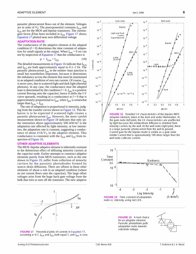
These characteristics may be seen in thedata shown in Figure 16. This data was tak-en with and without light shining on a near-by hole in the metal covering of the adaptiveelement, to illustrate that the currents in thecapacitor node (Vf) are unaffected by mi-nority carriers generated in the substrate.
The I–V relationship for the element isgiven by
(17)
where I is the current flowing onto the ca-pacitor. I consists of three components, theMOS transistor current Im, the bipolar tran-sistor current Ib, and the parasitic photocur-rent in the emitter–base junction Ipar. The
I Im Ib – Ipar+=
∆V Vo Vf –≡
Im I0,m eκ∆V
e1 κ–( ) ∆V–( )
–[ ]=
Ib I0,b e∆– V
1–[ ]=
FIGURE 14 Expansive adaptive element (a), shown in two schematic forms, along with the capacitor that stores the adaptation state.
(b) The mode of conduction when the output voltage is higher than the capacitor voltage: The structure acts as a diode-connected MOS transistor.
(c) The opposite case: The p+/n junction is forward-biased, and the device as a whole acts as a bipolar transistor with two collectors.
Analog VLSI Phototransduction CNS Me
FIGURE 15 Measured current–voltage relationship for the new expansive adaptive element shown in Figure 14. The bipolar mode conduction e-folds every 28 mV, compared with 48 mV for the MOS mode, leading to a quantitative difference in the voltage at which the current rapidly increases. At any scale of current, the curves have the same appearance; the voltage scale changes logarithmically with the current scale. This data was taken from a p-well chip.
mo #30 T. Delbrück & C.A. Mead
ADAPTIVE ELEMENT Apr 2, 1996 9
Cur
rent
(A
)
0 0.2 0.4 0.6 0.8 1
Gate node
10 -13
10 -12
10 -11
10 -10
10 -9
10 -8
10 -7
10 -6
10 -5
10 -4
10 -3
0 0.2 0.4 0.6 0.8 1
|∆V| (V)
Well node
10 -13
10 -12
10 -11
10 -10
10 -9
10 -8
10 -7
10 -6
10 -5
10 -4
10 -3
Light and DarkCurves
Superimposed
Light
Dark
Bipolar
MOS
Bipolar
MOS
I0=10-16 – 10-15 A
e-fold48 mV
e-fold28 mV
|∆V| (V)
10 0
10 1
TimeConstant
(s)Darkness
parasitic photocurrent flows out of the element. Voltagesare in units of VT. The preexponential constants I0,m andI0,b are for the MOS and bipolar transistors. The current-gain factor β has been included in I0,b. Figure 17 showsEquation 17 plotted near zero differential voltage.
ADAPTATION RATEThe conductance of the adaptive element at the adaptedcondition (I = 0) determines the time constant of adapta-tion for small signals at the output. When Ipar = 0 we cansee by inspection of Equation 17 that the conductance is
(18)
The detailed measurements in Figure 16 indicate that I0,mand I0,b are both approximately equal to 0.1–1 fA. Theparasitic photocurrent Ipar in the emitter–base junction issmall but nonetheless important, because it determinesthe imbalance across the element that must be maintainedin an adapted condition of zero net current. Of course, Iparis never zero, due to scattered light and dark light (thermalphotons). In any case, the conductance near the adaptedstate is determined by the condition I = 0. Ipar is a positivecurrent flowing onto the capacitor; hence it shifts the I-Vcurve upwards, resulting in a conductance at I = 0 that isapproximately proportional to Ipar, when Ipar is somewhatlarger than I0,m + I0,b.
The rate of adaptation is proportional to intensity, judg-ing from the transfer curves shown in Figure 12. This be-havior is to be expected if scattered light creates aparasitic photocurrent Ipar. However, the more carefulmeasurement shown in Figure 18 indicates that only un-der intensities above approximately 500 mW/m2 is theadaptation rate affected by light intensity; at low intensi-ties, the adaptation rate is constant, suggesting a conduc-tance of about 4 fA/VT in the adaptive element. Thisconductance is consistent with the I0,m and I0,b from in-spection of Figure 16.
OTHER ADAPTIVE ELEMENTSThe MOS–bipolar adaptive element is inherently resistantto the deleterious effect of diffusing minority carriers atthe capacitor node. Earlier attempts to construct adaptiveelements purely from MOS transistors, such as the oneshown in Figure 19, suffer from collection of minoritycarriers by the parasitic photodiodes formed bysource–drain diffusions. There are offsets in these otherelements of about a volt in an adapted condition (whereno net current flows onto the capacitor). The large offsetvoltages arise from the huge back-gate voltage from thebulk that tries to turn off the transistor. The new adaptive
g I0,m I0,b+=
Analog VLSI Phototransduction CNS Me
Im
IbI
-2
2
-1
1
∆V
FIGURE 16 Detailed I–V characteristics of the bipolar–MOS adaptive element, taken in the dark and under illumination. At the gate node (left plot), the I-V characteristics are unaffected by light because the emitter/drain diffusion is shielded from minority carriers by the well. At the well node (right plot), there is a large parasitic photocurrent from the well to ground. Current gain for the bipolar mode is visible as a gate node emitter current that is approximately 100 times larger than the well node collector current.
10 -1
-4 -3 -2 -1 0
(5 W/m2)
FIGURE 17 Theoretical plots of currents in Equation 17, assuming κ=0.7, I0,m and I0,b both equal 1, and Ipar is zero.
Log IntensityFIGURE 18 Time constant of adaptation node vs. intensity, using red LED.
mo #30
FIGURE 19 A bad choice for an adaptive element. Parasitic photodiode pulls adaptation node towards substrate voltage.
T. Delbrück & C.A. Mead

10 Apr 2, 1996 PHOTODIODE VS. PHOTOTRANSISTOR
p++ emitter
n well base
p– substrate collector
Photodiode (Cp)
(also hole in overlying metal)
StorageCapacitor(C1)
Feedbackcapacitor(C2)
Amplifier
Cascodetransistor
Adaptiveelement
Feedback transistor
6 µm
(Co)
element has offsets of less than 100 mV inan adapted state, owing mostly to the zeroback-gate voltage.
PHOTODIODE VS. PHOTOTRANSISTORPrevious logarithmic photoreceptor designsfrom the Mead lab all used the parasitic ver-tical bipolar transistor, shown in Figure 20,instead of a photodiode. We used the bipo-lar transistor because bipolars have muchless 1/f noise than MOS surface channel de-vices, and because the larger output currentis more capable of driving capacitive loads.Later on, when we started to use activefeedback circuits, we continued using bipo-lars for these same reasons.
Once we started to characterize the noise,we immediately discovered that 1/f noise isnegligible compared with shot and thermalnoise. In fact, there is a big disadvantage tousing bipolar phototransistors in the adap-tive receptor. The active feedback speeds upthe response by clamping the input node.When we use a phototransistor instead of aphotodiode, the feedback clamps the emit-ter node, but the base is left floating. Indeed,the base must not be clamped if the bipolartransistor is to function with its normal cur-rent gain mechanism. The current availableto charge and discharge the base of the tran-sistor is approximately the same photocur-rent available from the photodiode. As aresult, we obtain no speedup. The dynamicrange is at least 1–2 decades smaller with aphototransistor than with a photodiode. Inthe discussion of receptor noise, we shallsee that the noise properties of photodiodereceptors and phototransistor receptors areindistinguishable (page 15). In the contextof an active feedback circuit, it makes nosense to use bipolar phototransistors.
RECEPTOR LAYOUTFigure 21 shows the layout correspondingto the schematic in Figure 5. The photo-diode can be constructed from any of the pnjunctions that are part of a CMOS process,but the one that we use in practice is thejunction between native source–drain diffu-sion and substrate. In an n-well process, thejunction is between the p– substrate and then++ diffusion. We use this junction becausethe quantum efficiency is high and the ca-pacitance per unit area is relatively small,resulting in a fast response. This junctionalso has the advantage that it may be con-structed simply as an extension of thesource of Qfb. All parts of the circuit exceptfor the photodiode are covered with metal.
Analog VLSI Phototransduction
A nearby substrate contact sinks the photo-current to ground. The transistors in thefeedback amplifier are long, to maximizethe gain and hence the speedup. The adap-tive element is made from an isolated wellwith a single MOS transistor. The capaci-tive divider is formed from the two levels ofpolysilicon plus a metal plate, but a MOScapacitor may be used instead. The totalarea in this conservative layout is about80x80 µm2 in a technology with a 2-µmfeature size.
The capacitive-divider ratio determinesthe gain of the receptor for transient signals.The capacitance of the adaptive element it-self is usually not negligible compared withthe explicit feedback capacitor C2 and mustbe taken into account. It consists mostly ofthe active-well junction. A typical value is15 fF, equivalent to a square metal–poly ca-pacitor with an edge length of about 17 µm.
THE ILLUMINATION LIMIT (SPEED)From an evolutionary perspective, it is clearthat animals that can see in the dark occupyan important niche. The same is true for oursilicon receptors. If they can only be used inbright sunlight, then they are not very use-ful.
The source follower receptor has a re-sponse speed that is determined primarilyby the ratio of quantum efficiency to capaci-tance per unit area in the photodiode. Thelarger we make the photodiode, the larger
CNS Memo #30
the photocurrent, but the larger the capaci-tance. Since we are pretty much stuck witha fixed technology, we regard this speed as aconstant of the problem. †
In the devices available in an ordinaryCMOS process, the maximum receptorspeed is obtained from one of the substrate-junction photodiodes, because these havethe largest quantum efficiency and the low-est capacitance. We have chosen to use theactive–substrate diode rather than thewell–substrate diode in all of our designsbecause the layout is much more compact.We expect that the well–substrate diode willhave a similar capacitance and quantum ef-ficiency.
† The speed could be increased if we had access to PIN diodes 28, where the p and n regions are sepa-rated by an intrinsic region that increases the vol-ume, and hence the quantum efficiency, and simultaneously decreases the capacitance of the device—but we know of no CMOS process with these characteristics.In a typical 2-µm n-well process, the active-sub-strate capacitance is around 120 aF/µm2+200 aF/µm. In the more heavily doped 1.2-µm process, these values jump to 500 aF/µm2 + 400 aF/µm.
FIGURE 20 Parasitic vertical bipolar transistor in an n-well process.
FIGURE 21 Photoreceptor layout. This layout is nonoptimal because the feedback transistor is wider than it needs to be, leading to excessive Cfb (see page 5).
T. Delbrück & C.A. Mead

THE DETECTION LIMIT (NOISE) Apr 2, 1996 11
(a)
(b)
(c)
Electronenergy
Floats tonecessarylevel
Bias Light
Photodiode
Outputvoltage
e–
A reasonable definition of the lower lim-iting intensity for operation of the receptoris the intensity at which the photoreceptorhas a rise time of 15 ms—corresponding tothe time for a single field of a video camerathat scans at 60 Hz, and approximately thesame as the cutoff frequency for human vi-sion under photopic† conditions. We cansee from Figure 10 that the fastest photore-ceptor circuit that we have tested has a risetime of 15 ms at about 1 mW/m2 irradi-ance—equivalent to an illuminance ofabout 1 lux††, or approximately the light-ing of the full moon. This receptor is builtwith a feedback amplifier with a gain ofseveral hundred, a closed loop gain ofabout 10, and a photodiode with an area of20 µm by 20 µm.
CCD detectors are integrating devices;every frame, they dump out all the chargethey collected since the last frame. Thesensitivity limit is determined by the elec-tron counting noise in the charge-sensingamplifier. Current commercial amplifiers,in consumer end-product devices, functionat a noise level of about 100 electrons,meaning that the RMS noise in the outputis equivalent to 100 electrons in the chargebucket. If we assume that the cameras musthave at least 4 bits resolution to be accept-able, then the number of electrons collect-ed must be 16 times the noise level, or1600, each 1/60 s. A typical CCD pixelarea is 100 µm2. The quantum efficiency isabout 30 %. From these numbers, we com-pute that the irradiance is 1.4 mW/m2, or1 lux at 555 nm, consistent with the adver-tised ratings††† of a few lux.
The borderline between rod and cone vi-sion occurs at an illuminance of about 1lux, which is approximately the level ofbright moonlight. In Figure 10, we have la-beled the rod-cone border and the moon-light irradiance.
In summary, the current photoreceptorcircuit functions down to about the sameintensities as consumer CCD cameras andhuman cone receptors.
ILLUMINATION LIMIT: HIGH ENDMOS transistors Qn and Qcas that form thebottom of the amplifier circuit in the adap-tive receptor contain parasitic photodiodesfrom their drains and sources to the sub-strate. Ordinarily, these parasitic photo-diodes are irrelevant, but under intense
† Photopic means cones vision, mesopic means cones and rods are both used, and scotopic means rod vision.†† At 555 nm wavelength (the peak of human sen-sitivity under photopic conditions), 1 lux = 1.4 mW/m2. For white light (uniformly distributed over visible), 1 lux=4 mW/m2=104 photons/µm2s. 21
††† Whatever these ratings mean—supposedly each manufacturer makes up their own definition, but none of them tell you what it is!
Analog VLSI Phototransduction
illumination the current to ground that theyproduce may exceed the bias current sup-plied by Qp, pulling the output node toground. This situation may be amelioratedby shielding the native-type transistors inthe amplifier from light using a metal wir-ing layer, and by surrounding them with aguard bar made from native diffusion that ispreferably tied to Vdd. (It doesn’t makemuch difference if you tie the guard bar toground or Vdd.) Guard structures are dis-cussed further starting on page 15.
THE DETECTION LIMIT (NOISE)What is the smallest signal that can be de-tected? How is this value affected by lightintensity, and by detector area? How doesthe performance compare with commercialCCD cameras and biological rods andcones? What is the physical basis for the re-ceptor noise?
We’ll investigate the noise properties ofthe receptors and their detection ability, em-pirically and theoretically. We’ll start em-pirically, with measurements of noiseproperties. These measurements show thatthe underlying behavior is very simple. Thesimplicity of this behavior motivates anequally simple theory that intuitively andquantitatively describes how noise works inlogarithmic photoreceptors.
EMPIRICAL OBSERVATIONSThe observations shown in Figure 23 weremeasured from the simple source-followerdetector shown in Figure 22. We capturedthe noise power spectra using two types ofstimuli, a steady illumination from an LEDand a white-noise source. We used the whitenoise source as a direct measurement of thereceptor transfer function. We did eachmeasurement at several levels of intensity,separated by decades. It is clear that allcharacteristics are well above the instru-mentation noise.
CNS Memo #30
The important observation is that the to-tal noise power, integrated over the entirepassband of the receptor, is a constant inde-pendent of intensity. The lower the intensity,the smaller the bandwidth of the receptor,but the larger the noise level within thepassband. The responses of the logarithmicreceptor to white noise stimulation showthat the shape of the noise spectrum is thesame as the shape of the receptor transferfunction, at each intensity level. But whilethe transfer function measurement showsthat the receptor contrast gain is constant,independent of intensity, the underlyingnoise behaves differently, becoming larger,the lower the intensity.
We know that the noise arises from with-in the receptor, and is not an artifact of themeasurement (for instance, from noise inthe LED light source). The reason is that theamplitude of the noise depends on the levelof intensity. If the noise arose from thesteady light source, then reducing the inten-sity by interposing neutral density filterswould result in a set of curves like the topset of curves in Figure 23 showing the re-sponse to a white noise source. In otherwords, if the noise arose in the supposedlysteady source, then the bottom curveswould duplicate the top set of curves but beshifted down by a constant amount. Sincethe behavior is clearly quite different, weare certain that the noise arises in the detec-tor itself.
Another important observation is thatflicker noise (1/f) in the receptor is negligi-
FIGURE 22 The simple logarithmic photoreceptor used in the study of receptor noise. This circuit forms the input stage to the adaptive receptor. (a) shows the schematic form. The bias voltage sets a reference for the source voltage, which is the output. (b) shows that the compact receptor consists of a single MOS transistor whose source forms the photodiode. (c) shows the electron energy diagram. The source voltage floats to whatever level is required to spill the photocurrent over the channel and into the drain.
T. Delbrück & C.A. Mead

12 Apr 2, 1996 THE DETECTION LIMIT (NOISE)
Frequency (Hz)
(a)
0-1-2-3
0
-1
-2
(b)
(c)
1/ f
1/f2
-140
-120
-100
-80
-60
10-1
100
101
102
103
104
Sig
nal A
mp
litud
e (d
BV
/√H
z)
ble, although it is clearly dominant in the in-s t rumen ta t i on . One o f t en ge t s t heimpression from the literature that flickernoise dominates MOS transistor operation,but here it clearly does not.
The s econd s e t o f obse rva t i ons(Figure 24) compare the noise spectra of thesimple source-follower receptor and theadaptive receptor. We injected a small testsignal to examine the SNR degradation bythe adaptive feedback circuit. We can makethe following observations:1. The adaptive feedback circuit amplifies
both signal and noise, but degrades theSNR by less than 3 dB.
2. The feedback circuit and the cascodewiden the bandwidth; the extent of thewidening, a factor of 1.5 to 2 decades, isin agreement with earlier predictionsgiven in the discussion of the adaptivereceptor, that were based on the para-sitic capacitances and gain measure-ments.
The main conclusion of this measurement isthat the degradation of the SNR by theadaptive feedback circuit is small enoughthat our analysis can treat the feedback andadaptation as a noiseless amplifier. If wecan understand what determines the noisein the input stage of the adaptive receptorcircuit, then understanding the noise behav-ior of the complete adaptive receptor circuiti s t r iv i a l .
THEORY OF LOGARITHMIC RECEPTOR NOISEIn a logarithmic detector, the natural inputunits are fractions of the baseline signal,and the natural output units are fractions ofthe e-folding parameter. In the source-fol-
lower receptor, the gain of the receptor issimply per e-fold change inthe intensity, and hence the total dimension-less noise power P is given by
(19)
where ∆x2 means the mean-square variationof x. The reason we write the noise in theform of Equation 19 is that we shall derivean expression for the mean square variationin the charge sitting on the output node ofthe source-follower receptor. We will usethat expression in Equation 19 to obtain thereceptor noise.
There are two equivalent methods tocompute the charge fluctuation. The firstway uses the principle of equipartition fromstatistical mechanics. The second way ana-lyzes the statistics of the individual charges. USING EQUIPARTITION TO COMPUTE THE NOISE POWER. Theprinciple of equipartition says that the aver-age energy stored in each independent de-gree of freedom of a system in thermalequilibrium is . A degree of freedomis a parameter that appears quadratically inthe energy—for instance, each componentof the velocity of a free particle. Similarly,the charge on a capacitor is a degree of free-dom, because the energy stored on the ca-pac i t o r i s g iven by . Us ingequipartition, we can write the following re-lation between the fluctuations in Q and thetemperature:
(20)
VT kT q⁄=
P∆v
2
VT2
--------- ∆i2
Ibg2
-------- ∆Q2
C2⁄
VT2
----------------------= =≡
kT 2⁄
Q2
2C⁄
∆Q2
2C----------- kT
2------=
Analog VLSI Phototransduction CNS Memo #30
or
(21)Substituting this result in Equation 19, weobtain the total dimensionless noise powerfor the source-follower receptor:
(22)
The simplicity of this answer is quite re-markable. It says that the dimensionlessnoise power—namely, the noise expressedin input units—is the ratio of the unit chargeto the “thermal charge,” . In hind-sight, what else could it have been?
For a typical input capacitance of 100 fF,Equation 22 says that the total noise powerat room temperature is about 10-4, equiva-lent to an RMS variation of about 1 %.TOTAL NOISE IN ADAPTIVE RECEPTOR. The feedback circuit in theadaptive receptor adds minimal noise, but itdoes extend the bandwidth. The total recep-tor noise is hence increased to
(23)
where Ceff, given in Equation 7 (page 5), isthe effective input capacitance assuming asource conductance Ibg/VT at the source ofQfb. For a typical speedup of about 30(Table 1, page 6) the total noise is increasedby the same factor, leading to an RMS vari-ation of about 5 %.USING SHOT NOISE STATISTICS TO COMPUTE THE NOISE POWER. The equipartition computation may appearto be magic. Relying solely on this principlemay give one an uncomfortable feeling thatsomething has been left out. That some-thing is the intuition and understanding ofthe origin of the noise, and why it takes theinteresting form given by Equation 22.
∆Q2
kTC=
PkTC C
2⁄
VT2
---------------------qVT C C
2⁄
VT2
--------------------------- qCVT -------------= = =
CVT
Pq
CeffVT -------------------=
FIGURE 23 Noise spectra for the source-follower logarithmic receptor shown in Figure 22, at different intensities. The curve labeled (a) is from an isolated follower pad, and shows that the measured 1/f instrumentation noise in the follower pad and spectrum analyzer is smaller than measured spectral noise from the detector. The curves labeled (b) show the intrinsic noise spectra from the receptor at a given level of steady background intensity. The number by each curve is the log background irradiance. 0 log irradiance is 1.7 W/m2. The lower of each smooth curve is the theoretical fit based on the theory given in the text; the upper curve is twice the theoretical value. The curves labeled (c) show the response of the receptor to small-signal white-noise stimulation from an LED. The stimulus for each curve has the same contrast, i.e., it is formed by interposing neutral density filters between a white noise source and the receptor. The straight lines have a slope of 1/f 2 , the same as from a first-order low-pass filter. The number by each curve is the log background irradiance. Definition of dBV units is the signal power, in dB, relative to a 1 V signal. Parameters used in the fits: node capacitance C=341.2 fF, temperature T=300°K, and time constant τ chosen to make cutoff frequency correct at the brightest intensity. τ is scaled inversely with intensity for the other curves. The capacitance consists of a 20x20 µm2 photodiode with areal capacitance of 0.122 fF/µm2 and edge capacitance 0.451 fF/µm (total 85 fF), a 6x6 µm2 gate with areal capacitance 0.828 fF/µm2 (oxide thickness 417 Å, 29 fF), and a metal wire with total capacitance 92 fF.
T. Delbrück & C.A. Mead

THE DETECTION LIMIT (NOISE) Apr 2, 1996 13
-140
-120
-100
-80
-60
-40
10 0 10 1 10 2 10 3 10 4
Frequency (Hz)
Am
plit
ude
(dB
V/√
Hz)
1/f1/f 2
Instrumentation
Source follower
Adaptive receptor
withCascode
withoutCascode
The macroscopic flow of current throughthe receptor circuit consists of the micro-scopic movement of discrete charges. Asshown in Figure 25(a), single chargescause step changes in the voltage on the ca-pacitor. The charges are collected by thephotodiode and leave via the channel of thefeedback transistor. The time at which acharge appears, and the time that it stays onthe capacitor, are both random. A givencharge spends a random amount of time sit-ting on the output node. These times aredistributed according to a Poisson distribu-tion.
Each charge is independent of all theothers, which means that if we can com-pute the statistics of the average charge,then we can easily obtain the statistics ofthe current as a whole. We shall first com-pute the average noise energy in the stepchange of charge caused by a singlecharge. Using the independence of thecharge events, we shall then compute thenoise power in a current that consists of aflow of single charges.
The amplitude of the step change is theunit charge q of a single electron. The noiseenergy contained in the step is the integralover time of the squared deviation of thecharge from the mean value. The mean val-ue is zero, since this single charge has finiteduration. During the presence of thecharge, the value is simply q, the size of thecharge. Hence, the mean value of the noise
Analog VLSI Phototransduction
energy is given by , where is themean length of time that the charge ispresent. Hence, the noise energy in a singleevent is given by
(24)The current consists of a random stream ofsingle events. All the events are indepen-dent, so we can compute the mean squarecharge fluctuation (the noise power)in the signal by taking the noise energy in atypical event given by Equation 22 andmultiplying by the average number ofevents per unit time, given by :
(25)
We can think of the preceding computationin two ways: Either as an average of a singleparticle over many lifetimes, or as an aver-age of many particles over a single lifetime.The two viewpoints lead to identical results;the former is perhaps more rigorous interms of obtaining the correct multiplier,while the latter offers a better intuition ofwhat process physically governs the noisebehavior—an average over a time window.Formally, the equivalence of the two ap-proaches arises from the ergodicity of thesystem.
A crucial fact is that the average lifetime of a charge is the same as the time con-
stant of the node—a fact that is obvious buthard to prove. The reason it is true is that thetime constant describes the time scale of the
response of the node to a disturbance. If thedisturbance consists of a sudden excessamount of charge on the node, the systemreturns to its equilibrium level after sometime—the time being the average lifetimeof the individual charges that make up thedisturbance. The decay from the excess isexponential, and the e-folding time is onceagain . Hence, in Equation 25 we can re-place with the time constant of the sub-threshold circuit, , to obtain
(26)
which is the same result as Equation 21, ob-tained using equipartition. Notice that herewe have suddenly slipped thermal behaviorinto a discussion that was strictly statistical.Boltzman statistics determines the timescale of the integration, which in turn deter-mines the total noise.SHOT VS.THERMAL NOISE? Whenwe initially attempted to compute the noisein the receptor, our theory consistently dif-fered from the measured noise power by afactor of about two—our theory always pre-dicted a noise power twice what we mea-sured. This distressing situation was notresolved until Rahul Sarpeshkar pointed outthat shot and thermal noise are alternativeaspects of a single underlying phenomenon.We had been under the impression that they
q2τ τ
E q2τ≡
∆Q2
Ibg q⁄
∆Q2
EIbgq
------- q2τ
Ibgq
------- qIbgτ= = =
τ
ττ
CVT Ibg⁄
∆Q2
qIbg
CVTIbg
-----------=
qCVT qCkTq
------ kTC
=
= =
FIGURE 24 Comparison of noise spectra for simple source follower detector of Figure 22 and the adaptive receptor shown in Figure 5, with the layout shown in Figure 21. The gain of the source follower receptor is about 60 mV per decade. The gain of the adaptive receptor is about 1.3 V/decade, or 27 dB more than the gain of the source follower receptor. The plots show the measured power spectra for each detector, along with the spectrum of the follower pad instrumentation. The DC irradiance for this measurement is 0.2 W/m2, and the injected signal is a combination of a 150 Hz sinusoidal signal and a 1.5 kHz signal each with Rayleigh contrast of about 1 %. We can see from the height of the signal spike relative to the surrounding noise that the SNR for each detector are nearly indistinguishable. For definition of dBV units, see Figure 23.
τq
Mean level(a)Time
Cha
rge
Averagelifetime
(b)
FIGURE 25 Shot noise computations. (a) The flow of current in the source-follower receptor consists of unit charges that appear and disappear, acting independently. (b) A single charge appears at a random moment, lasts a random amount of time, and disappears. The distribution of times that the impulse lasts is described by a Poisson process. The mean charge level is zero. The average energy in the impulse is q2τ.
CNS Memo #30 T. Delbrück & C.A. Mead

14 Apr 2, 1996 THE DETECTION LIMIT (NOISE)
-100
-80
Noi
se (
dB
V/√
Hz)
1 /f 2
Signal
-100
-90
-80
FIGURE 26 Photodiode and phototransistor noise properties are indistinguishable, and bandwidths are identical with passive feedback. The stimulus is a steady background with a small AC component. The test signal has the same SNR for each device.-140
-120
101
102
103
Sig
nal +
Frequency (Hz)
Instrumentation
1/f
-120
-110
500 600 700Frequency (Hz)
were separate phenomena, with identicalmagnitudes. We computed the shot noise,and then insisted that the thermal noise wassomething additional—which is wrong.
Perhaps the easiest way to see how shotand thermal noise are related is to considerthe flow of individual charges that make upa current. Looking at the current, we ob-serve an average arrival rate of ele-men ta ry cha rge s . The cha rges a r euncorrelated. Given an average arrival rate,and the fact that all the charges are indepen-dent, in some sense the statistics of the floware as random as they can possibly be. Howcould more noise be added? Only by intro-ducing additional correlations. An exampleis 1/f noise, where modulatory fluctuationsin the level of current contribute additionalnoise power. Temperature has no effect onthese statistical fluctuations; it serves onlyto set the bandwidth—the averagingtime—at which the system operates.EFFECT OF TEMPERATURE. I t mayseem odd that the total noise power given byEquation 22 is inversely proportional to thetemperature. Usually, we think that reduc-ing the temperature reduces the noise. Thisodd behavior is due to a bandwidth effect.When the temperature is reduced, the ther-mal voltage scale is also reduced. At a givenlevel of current, determined by the light in-tensity, the source conductance of the feed-back transistor is increased, and the timeconstant is reduced. Hence, reducing thetemperature increases the bandwidth. Thecircuit integrates over a smaller time scale,the current is observed with finer granulari-ty, the individual charges are more closelyresolved, and hence, the total dimensionlessnoise power is increased. We must recallthat we are talking about the dimensionlessnoise, given by Equation 19, that measuresnoise in input-referred units, and not thenoise voltage. We can see from Equation 19and Equation 22 that the mean-square out-put noise voltage is given by
(27)
which is proportional to temperature, butthe output noise voltage is not a relevantquantity by itself because it must be com-pared with the natural voltage scale givenby VT.NOISE SPECTRAL DENSITY. Theamount of noise power per unit band-width—the spectral density of the
Ibg q⁄
∆v2 qVT
C------------=
Analog VLSI Phototransduction
noise—is interesting, because it says howdetectable a signal is if we know that it oc-curs within some particular frequency band.
The noise fluctuations are spread over thespectrum of a first-order lowpass filter. Thepower spectrum (the power per unit fre-quency) is given by
(28)
The funny normalization constant ap-pears so that the integral over all frequen-cies is the total power P:
(29)
Within the passband of the lowpass filter,the spectral density of the shot noise is
(30)
or
(31)
We can attribute half of this noise power toeach terminal connecting to the capacitor,to obtain a well-known result given in allthe standard texts:
(32)
Equation 32 gives the shot noise power on anode arising from a single source of currentonto that node. However, there are subtle-ties involved in the indiscriminate use ofthis expression. Sarpeshkar analyzed thenoise properties of MOS transistors for bothsaturated and nonsaturated operating condi-tions in subthreshold operation, and showedthat Equation 32 applies to a MOS transis-tor only when the transistor is saturated.26 THE ESSENCE. From Equation 31, wesee that S has units of time: The spectraldensity of noise is proportional to the timeper unit charge. The less time betweencharges, the smaller the noise. If we observethe signal over the time scale corresponding
to the transit of a single charge, then itmakes sense that the noise is approximatelyunity. At a current of 1 nA, the spectralnoise density from Equation 31 is approxi-mately 1 ns. The noise power is unity if weobserve the signal over a time scale of 1 ns,and it decreases linearly with the time overwhich the signal is averaged.
MEASUREMENT AND THEORYWe can compare the measured spectra ofthe source-follower receptor with the theo-retical spectrum. The three fit parametersare the temperature T, the capacitance C,and the integration time constant τ—whichscales inversely with intensity. After ac-counting for all node capacitance using pa-rameters supplied by MOSIS, assumingroom temperature operation, and choosingthe time constant to match the cutoff fre-quency of the measured spectrum for thebrightest intensity, we can see that the fit isvery good. The lower of the two theoreticalcurves is the predicted result; the uppercurve is twice the prediction. Another mea-sured receptor with a different capacitanceshows comparable results, although wedon’t show the data here because the resultsare so similar. Direct measurements of thecurrent noise spectrum in a single transistorconfirm these results with a single parame-ter fit.26
ASSUMPTIONS OF DIFFICULTY. Acommon phenomenon for people whostudy noise is to start with a pessimistic atti-tude that assumes that noise, inherently arandom phenomenon, is not quantifiable.The statistics of noise are just as quantifi-able as the statistics of the steady-state flowof current in a MOS transistor. In the case ofsteady-state current, we study statistics ofdiffusion—first-order statistics, while in theca se o f no i s e we s t udy s t a t i s t i c a lfluctuations—second-order statistics. It issatisfying to be able to quantify so preciselya phenomenon that initially seems intrinsi-cally random and unpredictable.
For more insight and detailed discussionabout electronic noise and photon counting,
S f( ) dPdf------- 4τP
1 2πfτ( )2+
----------------------------= =
4τP
S f( )df
0
∞
∫ P=
S 4τP 4CVT Ibg
------------- q
CVT -------------
= =
S4qIbg-------=
d∆I2
df------------ 2qI=
CNS Memo #30 T. Delbrück & C.A. Mead

MINORITY CARRIER DIFFUSION & GUARD STRUCTURES Apr 2, 1996 15
Lightspot
Well diffusion
Source-draindiffusion
Phototransistor 1 9/16" Distance
Sensing
Phototransistor
Guard bars
Probing light spot
Path of light spot
3 um
7 um
17 um
Sarpeshkar et al . 26 and Rose’s twobooks24,25 are helpful.
PHOTODIODE VS. PHOTOTRANSISTOR: NOISE BEHAVIOREarlier we saw that phototransistors have thedisadvantage that the base cannot bevoltage–clamped to speed up the response.Figure 1 shows that the noise properties ofphotodiodes and phototransistors are indis-tinguishable. The reason is obvious, giventhat the analysis just given may be directlyapplied to the base-emitter junction of thephototransistor.
NOISE ADVANTAGE OF CONTINUOUS-TIME RECEPTORS OVER SAMPLED DETECTORSContinuous-time logarithmic photorecep-tors have a natural advantage in noise per-formance over sampled detector systems.The advantage comes from the scaling ofbandwidth with intensity, so that circuit, in asense, adapts its integration time to howmuch signal is available. The less light thereis, the longer the integration time. The totalnoise is held constant.
In a CCD detector, the bandwidth is limit-ed by the sampling rate, because the pixelscannot store state across samples. This limit-ed integration time means that the number ofintegrated photons goes as the intensity. Thetotal noise power goes inversely with the in-tensity—it gets worse as the intensity de-creases instead of staying constant. There isnothing magical about it: the CCD detectorholds its bandwidth fixed while the log re-ceptor holds the number of integrated pho-tons fixed.
If we look at the spectral density of thenoise power, we see that there is no differ-ence: in both types of detectors the spectrumof the noise comes from the quantal natureof light and charge; in both, the noise spec-tral density goes inversely with the intensity.
One additional complication is that aCCD detector invariably uses a charge sens-ing amplifier to convert the photocharge to avoltage—the signal that is actually used.The noise in the charge-sensing amplifier isgenerally equivalent to a fixed number—onthe order of a hundred—of electrons at theinput. As the intensity decreases, the numberof integrated photocharges becomes compa-rable and then smaller than this fixed ampli-fier noise. For very low intensities, themean-square charge fluctuation in the outputsignal is fixed instead of decreasing linearlywith intensity. Here is a specific examplethat will make this idea clearer: Suppose theamplifier noise—the total RMS fluctua-tion—is equivalent to 100 photoelectrons.When the integrated number of photoelec-trons is 100, the fluctuation in the signal it-self is 10—a 10% variation. In reality,however, this small fluctuation in the signalis totally swamped by the amplifier noise.
Analog VLSI Phototransduction
The total noise is equivalent to a frac-tional variation of 100% of the signal!
Under dim lighting conditions, shotnoise dominates any detector system.The limited integration time of a CCDdetector means that shot noise is a reallimitation to the usable limit of opera-tion for video imagers, where the inte-gration time is at most 1/30 s. Atmoonlight illumination levels, the num-ber of charges collected per integrationtime is less than 1000. The shot fluctua-tion, 30, means that at best—with anoiseless amplifier—the noise level is3%, limiting the SNR to 30 dB.
MINORITY CARRIER DIFFUSION & GUARD STRUCTURESTurning now to an different topic, we’lldiscuss the diffusion of minority carri-ers and guard structures. We built thesimple structure shown in Figure 27specifically to measure lateral diffusionlength of minority carriers, and to testfor the effectiveness of various guardstructures in blocking their diffusion.The structure consists of a central para-sitic bipolar phototransistor surroundedon three sides by guard bars with differ-ent widths. The fourth side is left bare.The bipolar transistor acts as a probe forminority carriers by collecting and am-plifying the local concentration of ex-cess minority carriers in the bulk. Thischip was built in a 2 µm p-well technol-ogy. We measured the emitter currentusing a Keithley 617 picoammeter, witha 2 V collector-emitter bias.
The guard bars consist of two rectan-gles of ordinary p-type source–draindiffusion and a rectangle of p-well dif-fusion. All guard bars were grounded tothe bulk potential.
We imaged a 12 µm spot of light ontothe test structure at various locationsaway from the sensing transistor using asmall pinhole and the 100x objectivelens on the microscope. We moved thechip under the spot using a two-dimen-sional motorized positioning system.
The results of the measurements,Figure 28, show the measured current asa function of the distance of the test spotfrom the center of the sensing transistor.Each curve corresponds to movingacross a different guard structure.
For distances greater than approxi-mately 70 µm, the decay of carrier con-centration is exponential and themeasured e-fold distance is about 30µm. An exponential-decay approxima-
CNS Memo #30
tion is not good for short distances. The spaceconstant is shorter, the closer the spot to thesensor, probably because of geometrical ef-fects due to the finite size of the test spot orthree-dimensional effects of the interaction ofsurface recombination with the pure expo-nential decay. With no guard bar, the mea-sured current is reduced by a factor of 10 in adistance of about 40 µm.
To test for the possibility that this relativelylong diffusion length of 30 µm is due to scat-tering of light, and not minority carrier diffu-sion, we compared the diffusion lengthmeasured with a red and green LED. The ra-tio of absorption length for the red comparedwith the green LED is a factor of 2–3, so iflight scattering is a significant effect in themeasurement of diffusion length, we expect adifference between the diffusion lengths mea-sured with the two LEDs. There is no differ-ence. The decay with distance is nearly
FIGURE 27 Layout used to test for light-generated minority carrier diffusion and for the efficacy of various guard bars in blocking minority carriers. The large square in the middle of the figure is a parasitic bipolar transistor that probes for minority carriers.We shined a probing light spot onto the structure at various distances and directions away from the phototransistor and measured the current generated in the phototransistor. The guard structures consist of p-type diffusion in the n-type substrate. The 3 and 7 micron-wide structures are source-drain diffusion, and the 17 micron-wide structure is a p-well.
T. Delbrück & C.A. Mead

16 Apr 2, 1996 SPECTRAL SENSITIVITY
30020010000
20
40
60
80 (a) Effect of guard bars
Distance from center (um)
no guard3 µm diff7 µm diff17 µm well
2001000
-1
0
1
(c) Diffusion expt comparisionof Red and Green LED
Red LEDresponse withsuperimposedgreenresponse
3002001000
0
1
2
Cur
rent
(nA
)
no guard3 µm diff7 µm diff
17 µm well
(b) Effect of guard bars
log
Cur
rent
(lo
g n
A)
if no minority carriers
log
Cur
rent
(lo
g n
A)
indistinguishable, as shown in Figure 28c.This result is not very surprising becausethe absorption length for red and green lightcenters around 1 µm.
The guard bars were only moderately ef-fective in reducing the minority carrier den-sity. The widest guard bar, a 17 µm well,reduces the minority carrier density by up toa factor of 10, particularly when the testspot shines directly onto the guard bar. Theother two guard bars, which consist ofsource-drain diffusion, are less effective, re-ducing the carrier density by a factor of 2–3.Interestingly, the 3 µm guard bar seems tobe more effective than the 7 µm guard bar.We don’t know the reason for this result, butwe can repeat it. SUMMARY. We measured a diffusionlength of about 30 µm at distances of great-er than 70 µm from the source. A mini-mum-size silicon retina pixel has about thesame dimension, which means that minori-ty carriers can have a large effect on circuit-ry surrounding an opening in the overlyingmetal. The use of guard bars can reduce thenumber of minority carriers, but not by verymuch. Even a 17 µm-wide well—the deep-est available diffusion—can only reduce theminority carrier concentration by a maxi-mum factor of about 10. Circuits must beinherently resistant to the effect of excessminority carriers—like the adaptive ele-ment discussed earlier—if they are to func-tion correctly with light shining on the chip.
SPECTRAL SENSITIVITYThe absorption of light by silicon is wave-length-dependent: Short wavelength pho-tons travel a shorter distance, on theaverage, before being absorbed.† The ab-sorption length, L(λ), as a function of pho-ton wavelength λ, for bulk silicon, is shownin Figure 29. For blue light (wavelength475 nm) L is 0.3 µm, while for red photons(650 nm) L is 3 µm—a ratio of approxi-mately 10 in absorption length over the visi-ble spectrum. This behavior is primarilydue to the available density of states, be-cause there are many more available statesat higher energies.
The wavelength-dependent absorptionmeans that photodetectors formed fromjunctions with different junction depthshave different spectral responses. In a
† This effect is known to degrade resolution in CCD imagers at longer wavelengths. The longer-wavelength photons get absorbed deeper in the substrate, diffuse less precisely to the correct charge bucket, and take enough time to diffuse that they get collected into the wrong charge bucket. Many CCD imagers are built in a shallow p-well to reduce these effects and to better tailor the spectral response to match with human spectral efficiency.
Analog VLSI Phototransduction
CMOS process, there are a number of dif-ferent junctions with different doping anddepth. An ordinary CMOS process has twocomplementary source–drain active diffu-sions and a well diffusion. For concrete-ness, we consider an n-well process; thewell and the active diffusion for the nativetransistors are n-type, and the substrate andactive diffusions for the well transistors arep-type.†† We can form four photodetectorsin a plain CMOS process, the three photo-diodes plus a single parasitic PNP bipolartransistor, whose emitter is active, base iswell, and collector is substrate.
†† The complementary process, p-well, results in a set of devices that are exactly complementary to the ones we describe here, and we expect that these devices have similar characteristics.
Figure 30 shows a set of typical carrierconcentrations in the parasitic vertical bipo-lar for different photon absorption lengths.We computed the curves from the diffusionequation. The carrier concentration goes tozero at the edge of a junction. At the sur-face, the concentration is reduced by sur-face recombination. The junction current isproportional to the slope of the carrier con-centration at the edge of the junction. Long-wavelength light creates most carriers deepin the substrate, so the current is mostlyfound in the deepest junction. In contrast,short-wavelength light causes a currentmostly in the shallowest junction.
A BiCMOS process adds a medium-doped p-type diffusion intermediate indepth between the active diffusion and thewell diffusion. This new implant is used toform the p-type base for vertical NPN bipo-lar transistors.††† The emitter of the vertical
Distance from center (um)Distance from center (um)FIGURE 28 Results of measurements on diffusion test structure shown in Figure 27. (a) shows the measured photocurrent due to minority carrier diffusion as a function of the distance of the test spot from the sensing phototransistor. The different curves show the current for movement of the spot in different directions out from the middle of the phototransistor. (b) shows the same results on a log(current) scale. (c) shows a comparison between illumination with red and green light. The absorption for red light is much less than for green light, so if the results in (a) and (b) were due to scattered light and not minority carrier diffusion, we expect a difference in the measured diffusion length that we do not observe.
CNS Memo #30 T. Delbrück & C.A. Mead

SPECTRAL SENSITIVITY Apr 2, 1996 17
20 µm
Light
p++ n p–
L = 50 µm (IR)
L = 5 µm (Red)
L = 0.5 µm (Blue)Con
cent
ratio
n
10 -2
10 -1
10 0
10 1
102
10 3
10 4
10 5
0.4 0.6 0.8 1 1.2Wavelength l (µm)
Absorptionlength L (µm)
B G R IR
p– subs
n well
p++ active
1 V
p– subs
n well
1 V
1 V
1 V
1 V
1 V
well-substrate
active-well
active-p base
p base-well
p+ base
n++ emitter
3 µm
bipolar is the heavily-doped n-typesource–drain diffusion, and the collector isthe lightly-doped n-type well. In a BiC-MOS process, we can form an additionalfour photodetectors: two photodiodes fromthe base to the emitter and collector, plustwo vertical bipolars, one being the floatingNPN, the other the parasitic PNP that usesthe base diffusion as an emitter in a mannersimilar to the parasitic PNP discussed earli-er.
Of these eight devices, we measured thesix shown in Figure 31. We did not test thesimplest photodiode from native diffusionto substrate, because we neglected to fabri-cate it on the same chip in the same config-uration, making reliable results difficult toobtain. We expect it to behave similarly tothe well–substrate photodiode. Also, we
††† Only n-well BiCMOS processes exist; for technical reasons it is difficult to fabricate good floating vertical PNP bipolar transistors. Also, we note that a BiCMOS process differs from a true bipolar process in that it lacks an additional low-resistance implant in the collector (the well) to reduce collector resistance. The missing collector contact implant is not a concern for phototransis-tors, at least in the range in which we are inter-ested, because the generated photocurrents are much too small to generate appreciable ohmic voltage drop.
p
FIGURE 29 The photon absorption length as a function of photon wavelength at 300˚K. The absorption length is the distance over which 1/e of the incident photons are absorbed. Approximate wavelength of primary colors (B = blue, G = green, and R = red) from CIE color wheel, along with associated absorption length are shown as dashed lines. Dashed line at about 0.95 µm shows absorption length at peak of spectral response of deep, diffusion-limited junction (see page 18). (Adapted from Dash and Newman.3)
Car
rier
FIGURE 30 Theoretical carrier concentration profiles for the illuminated slab of silicon shown at the top of the figure. The plots show the excess minority carrier concentration as a function of distance into the silicon for three different photon absorption lengths. The junction current is proportional to the slop of the carrier concentration at the edge of the junction.
CNS Memo #30 T. Delbrück & C.A. Mead
arasitic PNP vertical NPN
Analog VLSI Phototransduction
FIGURE 31 The structures and biasing setups used to measure the quantum efficiencies of the devices. The upper four devices are photodiodes and the lower pair are phototransistors. In the text, we refer to the elements by the underlined names in the figure. The active junctions are shaded for each device. A scale bar is shows approximate dimensions (horizontal dimension not to scale).

18 Apr 2, 1996 SPECTRAL SENSITIVITY
10
100
0.3 0.4 0.5 0.6 0.7 0.8 0.9 1 1.1 1.2Wavelength λ (µm)
PhotopticVisibility
Monochromatorcalibration
parasitic PNP
vertical NPN
well-substrate
active-p base
p base-wellactive-well
Bandedge
(1.12 eV)
1
0.1
0.01
0.001
(cha
rges
/pho
ton)
B G R
3.75 2.81 2.25 1.88 1.61 1.41 1.25 1.13 1.02 .94Photon energy (eV)
see text
did not test the parasitic PNP that usesp–base as emitter because we forgot aboutit, although almost certainly its behavior issimilar to the usual parasitic PNP that usesactive as emitter.
A scale bar in Figure 31 shows the ap-proximate vertical dimensions of the junc-tions of this 2-µm feature size BiCMOSprocess, according to the MOSIS fabrica-tion service. The n++ emitter is arsenic-doped, with a junction depth of about0.3 µm, and a surface concentration of1020 cm–3. The p+ base is boron-doped,with a junction depth of 0.45–0.5 µm, and asurface concentration of 1–2·1017 cm–3.The n-well is phosphorous-doped with ajunction depth of approximately 3 µm, anda surface concentration of 3-4·1014 -cm–3.The p-type substrate has a doping of3–4·1014 cm–3.†
We distinguish between the deep, diffu-sion-limited detectors where the carriercollection volume is defined mostly by theminority carrier diffusion length, and theshallow, volume-limited detectors wherethe carrier collection volume is mostly de-fined by junction edges.
The aim of the measurement is to obtainthe absolute quantum efficiency Q(λ) foreach of the devices, as a function of photonwavelength λ, where Q(λ) is defined as:
(33)
The phototransistors have built-in currentgain; for them we count the collected charg-
† These parameters come from the specifications for the MOSIS 2–µm n-well BiCMOS process.
Q λ( )
# collected charges# incident photons at wavelength λ -----------------------------------------------------------------------------------
=
Analog VLSI Phototransduction
es including the gain, so Q(λ) can be largerthan 1.
We used a prism monochromator, in con-junction with a tungsten incandescentsource, to produce a continuously variable,nearly monochromatic source of light. Wehad to carefully calibrate several parame-ters to obtain a reliable measurement 6.
THE SPECTRAL RESPONSESFigure 32 shows the absolute quantum effi-c i ency ve r sus pho ton wave leng th .Figure 33 shows the same data on a linearscale. Figure 32 also shows the photopic(daylight) visibility curve, the band edge forsilicon, the monochromator bandwidth, andthe wavelengths of the primary colors. Wecan make several phenomenological obser-va t i ons .
• There is a clear distinction betweenphotodetectors that collect light-gener-ated carriers from a junction-limitedvolume and the photodetectors that col-lect light-generated carriers from a dif-fusion-limited volume defined by thediffusion length of minority carriers.The diffusion-limited detectors are moresens i t ive to longer wavelengths .
• The response spectra are broad band.All the detectors cover more than thevisible spectrum. Also, all of the detec-tors have responses that are flat within afactor of 2 or 3 within the visible spec-trum.
• The shallow junctions formed inside thewell are most sensitive to a wavelengtharound 500 nm, while the deep well-substrate junction sensitivity peaks atabout 900 nm, well outside the visible.
• The peak absolute quantum efficiencyfor the photodiodes varies from a highof about 0.8 at near-infrared photonenergy, to a low of about 0.3 for theshallow, volume-limited junctions.
•All the quantum efficiencies are approx-imately 0.3 at the blue end of the spec-trum.
• The phototransistor spectral responsesare very close to constant multiples ofthe deeper-junction responses contribut-ing to the base current for the pho-totransistor. For example, the parasiticPNP response is very similar in shape tothe response of the well-substrate junc-tion, but is completely unlike theresponse of the shallow active-welljunction. A similar observation can bemade for the vertical NPN. This obser-vation simply means that most of thebase current in the phototransistorscomes across the deep junction.
• The current gain is about 100 in the par-asitic bipolar phototransistor, and isabout 30 in the vertical bipolar pho-totransistor. This gain is a soft functionof the current level, and decreases atboth high and low intensities. Figure 34shows the current gain for the bipolar
FIGURE 32 Measured spectral quantum efficiencies Q(λ) versus photon wavelength and energy. The quantum efficiency is the number of collected charges per incident photon; it is larger than one for the phototransistors because they have built-in current gain. Each curve is labeled with the name of the device as shown in Figure 31. The small circles are the absolute calibration points measured with discrete LEDs. The photopic visibility curve shows the relative visibility of photons under photopic conditions; this curve is normalized to 1 at its maximum. The primary colors, according to the CIE color chart, are labeled on the wavelength axis. A shelf, marked with a hollow arrow, appears around the band edge for both the vertical NPN phototransistor and for the p base-well photodiode that forms the base to collector junction (page 19). The monochromator calibration curves show the spectral line width of the monochromator and the calibration wavelengths.
Qua
ntum
effi
cien
cy Q
(λ)
CNS Memo #30 T. Delbrück & C.A. Mead

PREVIOUS WORK Apr 2, 1996 19
0
0.2
0.4
0.6
0.8
1
0.4 0.5 0.6 0.7 0.8 0.9 1 1.1 1.2Wavelength (µm)
Qua
ntum
Effi
cien
cy
PhotopticVisibility well-substrate
active- p base
active-well
p base-well
0
50
100
150
200
10-10
10-9
10-8
10-7
10-6
10-5
10-4
10-3
10-2
ß-1 (IE/IB)
Parasitic PNP vertical bipolar
Vertical NPN bipolar
I (A)
transistors as a function of emitter cur-rent, measured by base-current injec-tion. These current gains are larger by afactor of about 2 than the spectral mea-surements.
•All of the spectral responses show anabsolute cutoff around the band edge.The cutoff is not perfectly sharp, andextends past the actual band edge. Thequantum efficiency drops off at a rate ofabout one e-fold per 25 meV aroundthe theoretical band edge. We are confi-dent of this result, because we used atwo point absolute calibration of wave-length, and we measured the mono-chromator bandwidth to be muchsmaller than the measured cutoffbehavior.
• There is an interesting shelf in the spec-tral response of the well to p–base junc-tion right around the band edge that canalso be seen in the NPN vertical bipolarresponse. It could be due to a shallowrecombination-generation centerunique to the p-base implant thatstretches out the spectral response anadditional fraction of an eV.
ABSOLUTE CURRENT LEVELPeople frequently ask how much current toexpect from a given size of photodiode orphototransistor. Since light intensity variesmore than 6 decades under photopic andmesopic conditions, the answer obviouslydepends on the operating conditions. Forreference we will compute a typical situa-tion. Office fluorescent lighting conditionsare an irradiance of an exposed surface ofabout 1 W/m2. Under these conditions,each 10 µm by 10 µm photodiode area,with quantum efficiency 0.5, generates acurrent
(34)
Typical moonlight is about 3 decades lesslight, and hence a photocurrent of only
1J s⁄
m2
--------- eV
1.619–×10 J
----------------------------× quantum2.5eV
---------------------
10µm( )20.5×
×
× 108quanta
s---------------- 25pA= =
Analog VLSI Phototransduction
25 fA (i.e. 25x10
-15
A), or approximately2.5x10
5
charges/second, or 4000 in 1/60 s.In sunlight, the irradiance can be as much as1 kW/m
2
, corresponding to a photocurrentof 25 nA. Optics and scene reflectanceproperties reduce these numbers by about afactor of 10 under typical conditions.
PREVIOUS WORK
The precursor for the work described here isan optical mouse system built by Dick Lyonat Caltech. He used precharged photodiodesto produce a digital signal at a time inverse-ly proportional to intensity. The system in-corporated gain control by precharging ofthe photonode after it had discharged to agiven level , and not at af ter a fixedin t eg ra t i on t ime .
Mead’s original logari thmicphotoreceptor
19
used a single parasitic verti-cal phototransistor that feeds into a series ofDarlington-connected lateral bipolar tran-sistors. A feedback arrangement convertsthe final current into a voltage that is loga-rithmic in the intensity. This receptor wasused in the Tanner and Mead optical flowchip. There was no good reason for usingthe lateral bipolar transistors.
The large area required by the lateral bipo-lar transistors quickly led to more compactdesigns. The early Mahowald and Mead sili-con retinas, and subsequently many otherMead lab projects, used a simple logarithmic
photoreceptor that consists of a parasitic ver-tical bipolar phototransistor, with a seriespair of diode-connected MOS transistors as aload
13
,
20
. This simple design has the virtuethat the layout is trivial and the receptor re-quires no bias controls. The signal producedby the recep tor has a ga in o f200–300 mV/decade of intensity. The twomain problems with this receptor which ledto the development of the adaptive devicesare
1.
A poor matching between differentreceptors. Signals output from neigh-boring receptors differ as much fromoffsets as from true signals caused bythe scene.
2.
A slow time-response, rendering thereceptor useful only under bright light-ing conditions and making all time-responses strongly intensity-dependent.
The SeeHear chip
22
, designed by Neilson,Mahowald, and Mead, was the first analogVLSI vision circuit that used the idea of ad-aptation. In that chip, the simple nonadapt-ing logarithmic receptors from the earlyMahowald-Mead silicon retinas were usedas input to Mead’s hysteretic differentiatorcircuit
18
. The problem with this arrange-ment is that the uncoupling of the receptorand adaptation is inefficient in terms oftransistor count, and forgoes the speedupadvantages of the active feedback arrange-ment.
Delbrück and Mead
8
built a preliminaryversion of an integrated adaptive receptorthat uses two stages of high-gain amplifica-
CN
FIGURE 33 Absolute quantum efficiencies plotted on a linear scale. Data are a subset of Figure 32.
E
FIGURE 34 Bipolar transistor current gain as a function of emitter current. Ordinate is ratio of emitter current to base current. Data is from n-well, double-poly, 2 µm feature size, BiCMOS MOSIS technology. Collector to emitter voltage was held at 1 V. Transistor dimensions in µm are given in the table below.
Base Collector EmitterParasitic PNP 20x20 diffusion limited 10x10Vertical NPN 10x10 20x20 8x8
S Memo #30 T. Delbrück & C.A. Mead
20 Apr 2, 1996 RELATION TO BIOLOGICAL PHOTOTRANSDUCTION
tion, one at the phototransducer, and theother in the feedback loop. This design hada large transistor count, lacked any speedupadvantage of the active feedback, and usedan inferior adaptive element.
Delbrück and Mead
7
built an adaptivesilicon retina for sensing time derivatives ofthe image contrast, using the same feedbackarrangement as described here, but lackingthe speedup advantage of using a photo-diode and a cascode, and using an inferioradaptive element. This silicon-retina chipuses the scanning mechanism to reset thepixel output every time the pixel output issampled.
Mead
17
built an adaptive silicon retinathat uses ultraviolet light to move chargeonto and off floating gates for storage of an-alog mismatch compensation. A pho-totransistor with a drain-type load produceshigh voltage gain at the input, and this highgain point is used in the UV adaptation. Un-fortunately, making high gain at the input isincompatible with high speed operation,and inherently prevents the type of voltage-clamping speedup we have discussed. Sub-sequent work has tended away from UV ad-aptation, because of technical problemswith shining high-energy photons onto thechip and making the circuit function cor-rectly at the same time.
Mahowald
12
incorporated the feedbackarrangement described here into a siliconretina with interesting network feedback.Her receptor does not have the speedup ad-vantage of the active feedback, and uses aninferior compressive adaptive element,leading to very unsymmetrical adaptationrates for bright- and dark-going illumina-tion changes. Mahowald’s chip with the re-ceptor improvements we have discussedhere is in fabrication.
Mann
15
developed several adaptive pho-toreceptor circuits that are more flexiblethan the ones described here, in that theyhave an adjustable temporal passband.These receptors also use U.V. mismatchcompensation. They use a larger number ofcomponents than the receptor describedhere. They also lack the advantage of activespeedup and use inferior adaptive elements.
None of the previous photoreceptorswere satisfactorily characterized, in thesense that no one bothered to measure sim-ple engineering metrics like usable dynamicrange and sensitivity.
Up until lately, continuous-time analogphotoreceptors have not received a greatdeal of commercial attention. Nearly all ef-fort is concentrated on sampled imagerslike CCD video cameras. Photoreceptorsare used in very specialized applicationslike optical repeaters, where high integra-tion density and wide dynamic range are notso important compared with responsespeed, and where special fabrication tech-nologies are available that allow use of
tricks like PIN photodiodes and avalanchemultiplication.
RELATION TO BIOLOGICAL PHOTOTRANSDUCTION
In the introduction we discussed functionalcharacteristics of biological photoreceptorsand how they inspired the silicon version.Three characteristics stood out: The adap-tive properties, the gain control resulting inillumination independent contrast response,and the invariance of the response time to il-lumination.
In the silicon receptor, the adaptationstate is stored as a charge on a capacitor. Inrods and cones, the adaptation state is (atleast partially) stored as the internal calci-um concentration. The full story of photore-ceptor adaptation mechanisms is toocomplex for discussion here, but the ideathat there is an independent state variablefor adaptation state is similar in the siliconand biological receptors.
More germane is the invariance of re-sponse time to illumination, because herewe see some functional differences. Howdoes the response-time invariance comeabout? The enormous gain generated inrods comes from 3–4 amplification stages,each with modest gain. The gain of eachstage is at most a few hundred, but the com-bination of all stages results in a maximumgain that closes 10
6
ion channels in re-sponse to a single photon.
The gain of the rod is inversely propor-tional to intensity. The mechanism for thisgain control probably lies in a modest gainreduction of each stage of the amplification.A small change in the gain of each stage re-sults in a large change in the total gain. Eachstage has a fixed gain–bandwidth product:When the gain is reduced, the response timedecreases proportionally. The trick is thatthe total gain goes as the
power
of the num-ber of gain stages, and the total time re-sponse goes
linearly
with the number ofgain stages.
This multistage gain mechanism con-trasts with the silicon receptor, which hasonly a two-stage amplifier, one of which hasfixed gain. As shown earlier, this gainmechanism results in a fast response time,but the response time is also inversely pro-portional to the intensity. We have not elect-ed to try to build a silicon receptor withmultistage gain, in analogy with the biolog-ical mechanism, because the response timeis adequately fast already, and the log gen-erating mechanism in subthreshold opera-tion is so convenient. All the gain control inthe silicon receptor is done right at the input
stage, by the exponential I-V relationship atthe source of the feedback transistor. Thelogarithm gotten for free, courtesy of Boltz-man, is apparently not used for this samepurpose in biological receptors. The obvi-ous first guess, a membrane channel withdiode rectifying characteristics, is not whatthe cones or rods use.
SUMMARY
We have discussed a photoreceptor circuitthat is useful for continuous-time pho-totransduction. It consists of a logarithmicinput stage coupled to an adaptive feedbackcircuit. The feedback circuit produces anoutput with high gain for transient—andpresumably interesting—signals, and haslow gain for static signals, including circuitoffsets. The feedback also speeds up the re-sponse by clamping the input node voltage.
The receptor can be fabricated in an areaof about 70 by 70
µ
m
2
in a 2–
µ
m singlepoly CMOS process. The useful dynamicrange, which we arbitrarily define as therange over which the bandwidth is at least60 Hz, extends down to moonlight illumi-nation levels, or at least 1.5 decades morethan a plain logarithmic detector withoutactive feedback.
The receptor noise in a plain logarithmicdetector is almost exactly what is predictedby a simple noise theory that assumes thatthe noise is purely shot noise, with a band-width set by the conductance of the feed-back and the capacitance of the input node.The noise in the adaptive receptor is withina factor of two of this value.
TECHNICAL INNOVATIONS
The three technical improvements in the re-ceptor are as follows:
1.
Using a photodiode, instead of the pho-totransistor used in previous designs,increases the dynamic range by at leasta decade, without degrading signal qual-ity.
2.
Using a cascode transistor in the feed-back amplifier yields another 0.5–1decade dynamic range.
3.
Using a new adaptive element increasesthe adaptation time constant and thesymmetry of the receptor response tolight- and dark-going transients, com-pared to previous designs, which usedelements that were very susceptible tothe effects of parasitic minority carriers.
Analog VLSI Phototransduction CNS Memo #30 T. Delbrück & C.A. Mead

CONCLUSION Apr 2, 1996 21
We have also discussed two theoretical top-ics in which we have developed a muchclearer understanding:1. We quantitatively understand the physi-
cal origin and dominant sources ofelectronic noise in continuous-time log-arithmic receptors.
2. We quantitatively understand the limitson response speed that effectively limitthe lower end of the receptor dynamicrange.
CONCLUSION Operations that require spatiotemporalcomputation on noisy input data in realtime are a natural fit to analog VLSI. Wehave shown how to build a practical photo-receptor circuit that is suitable as a front-end transducer for analog VLSI vision sys-tems. The receptor is usable under photo-pic vision conditions. The continuoustransduction process leads to intensity-in-variant total noise that is within a factor oftwo of photon counting noise. Photorecep-tors of this general type will undoubtedlybe used in commercial vision systems,where designers will not be able to resistthe capability to link low-power, continu-ous-time computation together with trans-duction.
ACKNOWLEDGEMENTSWe acknowledge support from the ONRand by MOSIS, the ARPA silicon foundry.4David Van Essen inspired this detailedstudy (especially of the noise properties).Rahul Sarpeshkar made a crucial observa-tion about the relationship between shotand thermal noise. David Standley andDick Lyon provided helpful commentsabout the manuscript. Micah Siegel andSanjoy Mahajan pointed out that κ varia-tions affect the gain vs. intensity character-istics and their measurement discrepanciesinspired the discovery of the importance ofthe Miller effect in Qfb.
REFERENCES1. D.A. Baylor, G. Matthews, K.-W. Yau,
“Two components of electrical dark noise in toad rod outer segments,” J. Physiol. vol. 309, pp. 591–621, 1980.
2. R. G. Benson and T. Delbrück, (1991). Direction-selective silicon retina that uses null inhibition, in D.S. Touretzky, Ed. Advances in Neural Information Process-ing Systems 4. pp. 756–763.
3. W.C. Dash and R. Newman, “Intrinsic optical absorption in single-crystal ger-
Analog VLSI Phototransduction
manium and silicon at 77 ˚K and 300 ˚K,” Physical Review, vol. 99, pp. 1151–1155, 1955.
4. D. Cohen and G. Lewicki, “MOSIS—the ARPA silicon broker,” in Proceedings from the Second Caltech Conference on VLSI, California Inst. of Tech., Pasadena CA, pp. 29-44, 1981.
5. T. Delbrück, “Silicon retina with Correla-tion-Based, Velocity-Tuned Pixels,” IEEE Transactions on Neural Networks, vol. 4, no. 3, pp. 529–541, May 1993.
6. T. Delbrück, Investigations of Analog VLSI Phototransduction and Visual Motion Processing, Ph.D. Thesis, Dept. of Computation and Neural Systems, Cali-fornia Institute of Technology, Pasadena, CA, 91125, 1993.
7. T. Delbrück and C.A. Mead, (1991), Sili-con adaptive photoreceptor array that computes temporal intensity derivatives, in T.S. Jay Jayadev (ed.) Proc. SPIE, Infrared Sensors: Detectors, Electronics, and Signal Processing., vol. 1541, pp 92–99.
8. T. Delbrück and C.A. Mead, “An elec-tronic photoreceptor sensitive to small changes in intensity,” in Advances in Neural Information Processing Systems 1, D.S. Touretzky, Ed., San Mateo: Mor-gan Kaufman, pp. 720–727, 1988.
9. T. Horiuchi, J. Lazzaro, A. Moore and C. Koch, “A delay line based motion detec-tion chip,” in Advances in Neural Informa-tion Processing Systems 3, R. Lippman, J. Moody, D. Touretzky, Eds., San Mateo, CA: Morgan Kaufmann, pp. 406–412, 1991.
10. M.A. Mahowald, An Analog VLSI Sys-tem for Stereoscopic Vision, Kluwer Aca-demic Publishers: Norwell, Massachusetts, ISBN 0-7923-9444-5, 1994.
11. M.A. Mahowald, VLSI Analogs of Neu-ronal Visual Processing: A Synthesis of Form and Function, Ph.D. Thesis, Califor-nia Inst. of Tech., Dept. of Computation and Neural Systems, Pasadena CA, 1992.
12. M.A. Mahowald, “Silicon Retina with Adaptive Photoreceptor,” Proc. SPIE/SPSE Symposium on Electronic Sci-ence and Technology: from Neurons to Chips, vol. 1473, pp. 52–58, April 1991.
13. M.A. Mahowald and C.A. Mead, “Sili-con Retina,” in Analog VLSI and Neural Systems, by C. Mead, Reading: Addison-Wesley, pp. 257–278, 1989.
14. M.A. Mahowald and T. Delbrück, “Cooperative stereo matching using static and dynamic image features,” in Analog VLSI Implementation of Neural Systems, C. Mead and M. Ismail, Eds., Boston: Kluwer Academic Pub., pp. 213–238, 1989.
15. J. Mann, “Implementing Early Visual Processing in Analog VLSI: Light Adapta-tion,” Proc. SPIE/SPSE Symposium on Electronic Science and Technology: from Neurons to Chips, vol. 1473, pp. 128–136, April 1991.
16. C.A. Mead, “Neuromorphic Electronic Systems,” Proceedings of the IEEE, vol. 78, pp. 1629–1636, 1990.
17. C.A. Mead, “Adaptive Retina,” in Ana-log VLSI Implementation of Neural Sys-tems, C. Mead and M. Ismail, Eds., Boston: Kluwer Academic Pub., pp. 239–246, 1989.
18. C.A. Mead, Analog VLSI and Neural Systems. Reading, MA: Addison--Wesley, 1989.
19. C.A. Mead, “A Sensitive Electronic Photoreceptor,” In 1985 Chapel Hill Con-ference on VLSI, H. Fuchs, Ed., Rockville: Computer Science Press, pp. 463–471, 1985.
20. C.A. Mead and M.A. Mahowald, “A Sili-con Model of Early Visual Processing,” Neural Networks, vol. 1, pp. 91–97, 1988.
21. J.R. Meyer-Arendt, “Radiometry and Photometry: Units and conversion fac-tors,” Applied Optics, vol. 7, pp. 2081–2084, 1968.
22. L. Nielson, M. Mahowald, and C. Mead, “SeeHear,” in Analog VLSI and Neural Systems, by C. Mead, Reading: Addison-Wesley, chapter 13, pp. 207–227, 1989. (adapted there from 1987 International Association for Pattern Rec-ognition, 5th Scandinavian Conference on Image Analysis.)
23. R.A. Normann and I. Perlman, “The effects of background illumination on the photoresponses of red and green cones,” J. Physiol., vol. 286, pp. 509–524, 1979.
24. A. Rose, Concepts in Photoconductiv-ity and Allied Problems, InterScience Publishers (div. of John Wiley), p. 104, 1963.
25. A. Rose, Vision: Human and Electronic, Plenum Press: New York, 1973.
26. R. Sarpeshkar, T. Delbrück, and C.A. Mead, “White noise in MOS transistors and resistors,” IEEE Circuits and Devices, vol. 9, no. 6, pp. 23–29, 1993.
27. R. M. Shapley and C. Enroth-Cugell, “Visual adaptation and retinal gain con-trols,” in Progress in Retinal Research, N. Osborne and G. Chader, Eds., New York: Pergamon Press, vol. 3, pp. 263–346, 1984.
28. S.M. Sze, Physics of Semiconductor Devices, Second Edition, New York: John Wiley & Sons, chapter 13 and appendix I, 1981.
29. J.E. Tanner and C. Mead, “An Inte-grated Analog Optical Motion Sensor,” in VLSI Signal Processing, II, S.Y. Kung, Ed., New York: IEEE Press, pp. 59–76, 1986.
CNS Memo #30 T. Delbrück & C.A. Mead

22 Apr 2, 1996 REFERENCES
Analog VLSI Phototransduction CNS Memo #30 T. Delbrück & C.A. Mead

INDEX Apr 2, 1996 23
INDEXNumerics1/f noise 1160 Hz 11
Aabsolute current level in photodiode 19absorption length of light 16, 17adaptive element 8–10
adaptation rate 9capacitance of 10conductance of 9
area of adaptive receptor 10artificial lighting 3, 8BBiCMOS process
junction depths 18photodetectors 16
biological photoreceptorsadaptation state 20gain and adaptation characteristics 2gain mechanism 20invariance of response time 2, 20
bipolar transistorcurrent gain 18noise behavior 15structure 10using in adaptive receptor 10
Ccapacitance
of adaptive element 10of typical junction 10typical values in receptor 6
capacitance to quantum efficiency ratio 10capacitive divider 3, 4cascode
effect on time response and noise 4functions in adaptive receptor 4
CCD detector 11degradation by carrier diffusion 16
CMOS process, photodetectors can con-struct in 16
DDash and Newman 17dBV units 12density of states 16diffusion-limited volume 18doping of typical BiCMOS process 18
Eeffective input capacitance 5effective input conductance 5e-fold 3ergodicity 13
Ffeedback circuit
closed-loop gain 4total loop gain 5voltage gain 3
feedback circuit, noise in 12flicker noise 11fluorescent lighting, typical level of 19flying insects 1foveal resolution, need for in imagers 1full moon lighting 11
Gguard structures 15–16
Iimage contrast 2
Analog VLSI Phototransduction
Jjunction capacitance, typical 10junction-limited volume 18
Kκ(kappa) 3Llayout
area of adaptive receptor 10minimizing Miller effect 6of adaptive receptor 10used to test minority carrier diffusion 15
lighting of the full moon 11lux, relation to W/m2 11
MMahowald adaptive silicon retina 3Mahowald, Misha 19Mann, Jim 20Miller effect 4, 5
minimizing 6minority carrier diffusion 15–16
effect of diffusion on high illumination limit 11
effect of lifetime on receptor response speed 6
moonlight illumination level 11MOSIS 14, 18, 21
Nneutral density filters 4noise in receptor, see receptornoise, see receptor
Pphotodiode, absolute current level 19photometry 11photopic visibility 18PIN photodiode 10primary colors 17
Qquantum efficiency
definition 18discussed 18–19measured, plot of 18peak 18
Rratio of photodiode quantum efficiency to
capacitance 10receptor
effect of finite minority carrier lifetime 6gain-bandwidth product 20logarithmic, technological context 19noise 11–15noise in adaptive 12response time 6second-order behavior 7–8signal to noise ratio 13signal to noise ratio degradation by feed-
back 12simplest logarithmic 2source-follower 2spectral density of noise 14speedup 7speedup obtained by active feedback 5steady-state gain 4transient gain 4
resistor, impracticality of making in CMOS process 8
rod-cone border 11Rose, Al 15
SSarpeshkar, Rahul 13, 15shelf in spectral response of phototransistor
19signal to noise ratio in CCD video imager 15signal to noise ratio of photodiode and pho-
totransitor compared 14silicon retina 19single photon counting, relation to contrast 2SNR, see receptor, signal to noise ratiospectral density of noise 14spectral sensitivity 16–19speedup
definition 5subthreshold transistor law 3sunglasses 4Tthermal voltage 3VVT 3
CNS Memo #30 T. Delbrück & C.A. Mead

24 Apr 2, 1996 INDEX
Analog VLSI Phototransduction CNS Memo #30 T. Delbrück & C.A. Mead