AN1541 - Using the MCP19111 Design Tools
18
2013 Microchip Technology Inc. DS00001541A-page 1 AN1541 INTRODUCTION TO THE MCP19111 The MCP19111 is a stand-alone, mixed-signal, synchronous buck pulse-width modulator (PWM) controller for many step-down converter applications. The device combines high-voltage capability with precise analog technology and a PIC ® microcontroller core to develop flexible step-down DC-DC converter applications. Common applications include Point-of- Load (POL) converters, intelligent LED drivers and programmable battery chargers. The device is capable of efficiently converting 4.5V-32V input voltage down to an output voltage of 0.5V-3.6V. The 2A drive strength allows POL converters to be designed for high output current applications, such as servers, networking equipment, set-top boxes (STBs), telecommunication equipment and graphic cards. Using a simple resistor divider enables the device to step high-input voltages down to output voltages greater than 3.6V, while adding a current-sense resistor enables the device to become a regulated current source. This application note provides a walk through on the design example using the MCP19111 as a buck POL converter with supporting tools developed specifically for this device and application. The MCP19111 is packaged into a 28-lead 5 mm x 5 mm QFN. It provides several GPIO pins and supports program debugging. Many of these applications require a high level of integration to minimize cost and circuit board area. By using the advanced digital and analog features of the Microchip proprietary process, many of the desired customizable attributes of POL converters are integrated into the MCP19111. Solutions that exist today require external resistors and capacitors to set switching frequency, current limit, control system compensation and delay time between power MOSFET switch control. By using the latest enhanced PIC core, the MCP19111 uses the digital attributes of the Microchip proprietary process to make these features user programmable through a simple graphical user interface (GUI). The ability for system designers to configure application-specific features allows the MCP19111 to be offered in a smaller package than the currently available POL devices. The GPIO of the MCP19111 can be used to develop proprietary features or configured to offer a power good output, device enable, switching frequency synchronization input/output, output voltage margining or even a device status or “heartbeat”. This flexibility allows the MCP19111 package and complete solution to be smaller, thereby saving size and cost of the system printed circuit board. Several software tools have been developed to assist in managing the flexibility of the MCP19111, including a Microsoft ® Office Excel ® -based design analyzer, as well as a graphical user interface. A full introduction of these tools and their strengths are included later in this application note. DEVELOPING STEP-DOWN DC-DC CONVERTER SOLUTIONS USING MCP19111 Similar to any power management circuit design, the application must be well defined to begin the design process. Several tools were developed to expedite the design and validation process for MCP19111 step- down DC-DC converter applications. The steps required for the design are outlined in the following sections. DESIGN INPUTS Input Voltage (Minimum and Maximum steady-state voltages are needed) The input voltage range is typically well known for most systems. In some cases, there may be distribution voltage drops in the system that lowers the V INMIN . The maximum steady state V IN is used for worst case power dissipation, while the maximum peak transient voltage should be considered for robustness. Output Voltage (Minimum and Maximum steady state voltage are needed if V OUT is variable) Typically, V OUT is a fixed value, but in some applications, the DC-DC converter output voltage can be programmed to match certain load requirements or for margining the system. Author: Terry Cleveland, Microchip Technology Inc. Using the MCP19111 Design Tools
Transcript of AN1541 - Using the MCP19111 Design Tools
AN1541Using the MCP19111 Design Tools
INTRODUCTION TO THE MCP19111
The MCP19111 is a stand-alone, mixed-signal,synchronous buck pulse-width modulator (PWM)controller for many step-down converter applications.The device combines high-voltage capability withprecise analog technology and a PIC® microcontrollercore to develop flexible step-down DC-DC converterapplications. Common applications include Point-of-Load (POL) converters, intelligent LED drivers andprogrammable battery chargers. The device is capableof efficiently converting 4.5V-32V input voltage down toan output voltage of 0.5V-3.6V. The 2A drive strengthallows POL converters to be designed for high outputcurrent applications, such as servers, networkingequipment, set-top boxes (STBs), telecommunicationequipment and graphic cards. Using a simple resistordivider enables the device to step high-input voltagesdown to output voltages greater than 3.6V, while addinga current-sense resistor enables the device to becomea regulated current source.
This application note provides a walk through on thedesign example using the MCP19111 as a buck POLconverter with supporting tools developed specificallyfor this device and application.
The MCP19111 is packaged into a 28-lead 5 mm x5 mm QFN. It provides several GPIO pins and supportsprogram debugging. Many of these applicationsrequire a high level of integration to minimize cost andcircuit board area. By using the advanced digital andanalog features of the Microchip proprietary process,many of the desired customizable attributes of POLconverters are integrated into the MCP19111.Solutions that exist today require external resistors andcapacitors to set switching frequency, current limit,control system compensation and delay time betweenpower MOSFET switch control. By using the latestenhanced PIC core, the MCP19111 uses the digitalattributes of the Microchip proprietary process to makethese features user programmable through a simplegraphical user interface (GUI).
The ability for system designers to configureapplication-specific features allows the MCP19111 tobe offered in a smaller package than the currentlyavailable POL devices. The GPIO of the MCP19111can be used to develop proprietary features orconfigured to offer a power good output, device enable,switching frequency synchronization input/output,output voltage margining or even a device status or“heartbeat”. This flexibility allows the MCP19111package and complete solution to be smaller, therebysaving size and cost of the system printed circuit board.
Several software tools have been developed to assistin managing the flexibility of the MCP19111, including aMicrosoft® Office Excel®-based design analyzer, aswell as a graphical user interface. A full introduction ofthese tools and their strengths are included later in thisapplication note.
DEVELOPING STEP-DOWN DC-DC CONVERTER SOLUTIONS USING MCP19111
Similar to any power management circuit design, theapplication must be well defined to begin the designprocess. Several tools were developed to expedite thedesign and validation process for MCP19111 step-down DC-DC converter applications. The stepsrequired for the design are outlined in the followingsections.
DESIGN INPUTS
Input Voltage (Minimum and Maximum steady-state voltages are needed)
The input voltage range is typically well known for mostsystems. In some cases, there may be distributionvoltage drops in the system that lowers the VINMIN. Themaximum steady state VIN is used for worst casepower dissipation, while the maximum peak transientvoltage should be considered for robustness.
Output Voltage (Minimum and Maximum steady state voltage are needed if VOUT is variable)
Typically, VOUT is a fixed value, but in someapplications, the DC-DC converter output voltage canbe programmed to match certain load requirements orfor margining the system.
Author: Terry Cleveland,Microchip Technology Inc.
2013 Microchip Technology Inc. DS00001541A-page 1

AN1541
Output Current Range
It is very important to know the maximum load currentfor developing the DC-DC converter. If the load issignificantly higher than what the power supply isdesigned for, changes to the footprint of the externalMOSFET, switches or to the inductor physical size maybe necessary.
Design Goals
Typically, the system design goals are identified early inthe design process. Trade-offs between efficiency, sizeand dynamic response must be made. High efficiencyis expected, but size and cost are also consideredwhen developing non-isolated step-down DC-DCconverters.
Higher switching frequency generally results in lowerefficiency, but leads to a smaller, faster respondingdesign. Typically, a balance between these two isaccomplished. Using Microchip’s MCP19111 deviceand supporting design tools help optimize the solutionwith the first pass hardware.
Power Train Calculations
• Switching Frequency Selection (based on design goals)
Switching frequency selection is based on manyvariables. For high-voltage input, hard switchingstep-down DC-DC converters, switching lossesare appreciable as shown in the MCP19111Design Analyzer. Optimizing switchingfrequency is critical to meet the design efficiencyand size targets.
• MOSFET Technology Selection (Cost vs. Efficiency vs. Size)
New MOSFET technology is available toincrease the design efficiency. MicrochipTechnology Inc. introduced a new generation oflow-resistance, low-capacitance MOSFETdevices that reduce the switching time bylowering the switch capacitance for anequivalent on resistance. This technologyresults in lower switching losses for similarconduction losses.
• Inductor Technology Selection
Several inductor types are available for step-down DC-DC converters. Typically, the corelosses are low for the ferrite or compositemagnetic core. The inductor’s DC resistancealso plays an important role in converterefficiency, and is taken into consideration in theMCP19111 Design Analyzer tool.
• Capacitance Technology Selection
Low equivalent series resistance (ESR)capacitors are recommended for both input andoutput use in high-frequency DC-DC converterdesign. The input capacitor ripple current isdiscontinuous, leading to high input ripplevoltage. The MCP19111 Design Analyzer takesthe maximum ripple current into account whencalculating efficiency and input capacitancevalue.
Even though the buck output current iscontinuous, many of today's designs use low-inductance values, resulting in high-ripplecurrent. Using low ESR capacitors reduces theoutput ripple voltage. The MCP19111 DesignAnalyzer uses input voltage, output voltage,output capacitance and output capacitance ESRto calculate the system efficiency and controlsystem bode plot.
Control System Design
• Stability vs. Performance Design
Adjustable integrated peak current mode controlis used in the MCP19111 device. The peakcurrent control system design is forgiving,making the converter easy to stabilize. Whenoptimizing the control system for speed, thisstability can be compromised. Carefulevaluation of the control system andmeasurements should be taken to ensure thedesign is stable over the entire range ofoperation.
• The MCP19111 Design Analyzer is a good way toquickly evaluate the control system. There is agood correlation between the analyzer and labresults.
• Testing is the last step in the design of the controlsystem. Two test methods are used: step loadperformance and bode plot analysis. The stepload testing consists of load-stepping the output ofthe step-down DC-DC converter and measuringthe output voltage perturbation. Sinusoidal outputringing indicates a low-phase margin system;output voltage oscillation indicates an unstablesystem. The bode measurement analysis requiresspecial equipment to inject an isolated AC signalinto the control system and measure the systemresponse. A network analyzer is required for thistype of testing.
DS00001541A-page 2 2013 Microchip Technology Inc.

AN1541
INTRODUCTION TO THE DESIGN TOOLS
The following additional documents and tools areavailable to help users in their designs:
• MCP19111 Data Sheet – “Digitally EnhancedPower Analog Controller with Integrated SyncDriver” (DS22331). This document includes all ofthe necessary specifications and informationrequired to develop a DC-DC solution using theMCP19111.
• MCP19111 Design Analyzer. This tool is used toinput application variables while it computes thedesired external components (e.g. switches,inductor and capacitors) and assists in setting theinternal configuration of the part, includingdefining the control loop and protectionthresholds.
• MCP19111 MPLAB® X Integrated DevelopmentEnvironment Plug-in. This plug-in is used tointerface the MPLAB X IDE with the MCP19111.Many of the device’s capabilities can bedemonstrated using the GUI. For moreinformation, see “MCP19111 MPLAB® XIntegrated Development Environment Plug-inUser’s Guide” (DS52113).
• MCP19111 Evaluation Board (ADM00397). Theevaluation board can be used to become familiarwith the MCP19111 device while controlling twoswitches in a step-down DC-DC topology. See“MCP19111 Evaluation Board User’s Guide”(DS52109) for information on how to install andoperate the board.
Starting the Design
To get started, use the values in Example 1:
EXAMPLE 1:
Starting with the MCP19111 Design Analyzer Tool
A Microsoft Office Excel-based design spreadsheet isused to input variables and component values to assistin the design process. The spreadsheet is used tooptimize the POL synchronous step-down or Buckconverter design.
For specific input and extraction or calculation of data,the tool includes the following sheets:
• Input Parameters
• Components
• Efficiency
• Frequency Analysis
• GUI
INPUT PARAMETERS SHEET
This sheet is used during the design phase as a guide.All operating corners of the design can be analyzed byusing multiple iterations of the design parameter entrycells (shaded yellow). To do this, enter the parametersinto the table and evaluate the results for severaloperating conditions, including worst case corners.
Enter the input voltage, output voltage and outputcurrent of interest:
• The Switching Frequency of the converterdetermines the efficiency, transient response, sizeand cost of the design. The switching frequencyshould be evaluated carefully to optimize thedesign to the performance goals.
• The Input Voltage Ripple defines how much inputcapacitance and its equivalent series resistance(ESR) is necessary to meet the specified inputripple requirement.
• The Minimum Input Voltage is used to calculatethe undervoltage lockout setting for the system.
• The Step Load Parameters are used to define thedynamic performance of the system and indicatethe amount of output capacitance needed toachieve the desired transient response. TheMCP19111 control system uses an analog peakcurrent mode control. The load step is defined asthe load current step from a High Output Currentto the Low Output Current. The next step isentering the size of the overshoot desired for thisload step. Larger load current steps and smalleroutput voltage overshoot result in larger outputcapacitance and lower ESR to minimize theovershoot leading to a higher system cost.
The spreadsheet calculates the system operatingparameters, estimates and graphs the systemefficiency and plots the closed loop response of thesystem using a calculated bode plot. The equationsused to plot the estimated efficiency and boderesponse are detailed in Appendix A: “MCP19111Design Analyzer Tool”.
VIN = 12V (10V to 13.2V)
VOUT = 1.8V
IOUT = 0A to 20A (no airflow); 0A to 30A (1.52 m/s airflow)
DesignGoal
– Efficiency > 90% @ 25A (most common operating point).
2013 Microchip Technology Inc. DS00001541A-page 3

AN1541
FIGURE 1: MCP19111 DESIGN ANALYZER – INPUT PARAMETER PAGE
SYSTEM COMPONENTS
The next step in the design process is to select thepower train components by entering their basicparameters into the design spreadsheet. Rememberthat all cells shaded yellow should be selected by thedesigner.
In the System Components table as displayed inFigure 2, the calculated results are shown in the cellsshaded green. They represent component values thatmeet the design goals.
The cells shaded yellow are used by the designer toinput the actual values. These cells are used for theestimated efficiency and control system plots. Theinductance, output capacitance, input capacitance andcurrent sense filter are selected from this side of thesheet.
The Power Train Component Parameters table onthe right is for the MOSFET parameters and parasiticvalues of the passive components.
FIGURE 2: MCP19111 DESIGN ANALYZER – COMPONENTS SHEET FOR DEFAULT EVALUATION BOARD SETTINGS
DS00001541A-page 4 2013 Microchip Technology Inc.
AN1541
Microchip’s MCP87050 and MCP87018 MOSFETswere used for the high-side and low-side switches. TheMOSFET’s ON resistance (RDSON) and gate chargeare both critical parameters for design analysis. Thelow-side MOSFET body diode characteristics are alsoa key parameter for estimating the efficiency of theconverter. Refer to the MOSFET’s data sheet for moreinformation. The diode conduction time is the estimatedamount of time when the current is flowing through thelow-side switch body diode. This time can be adjustedby using the MCP19111 dead time adjust setting. Theinductor DC resistance and ESR of the input and outputcapacitors are also used for efficiency and controlsystem calculations. Refer to the component datasheet for more information on these values.
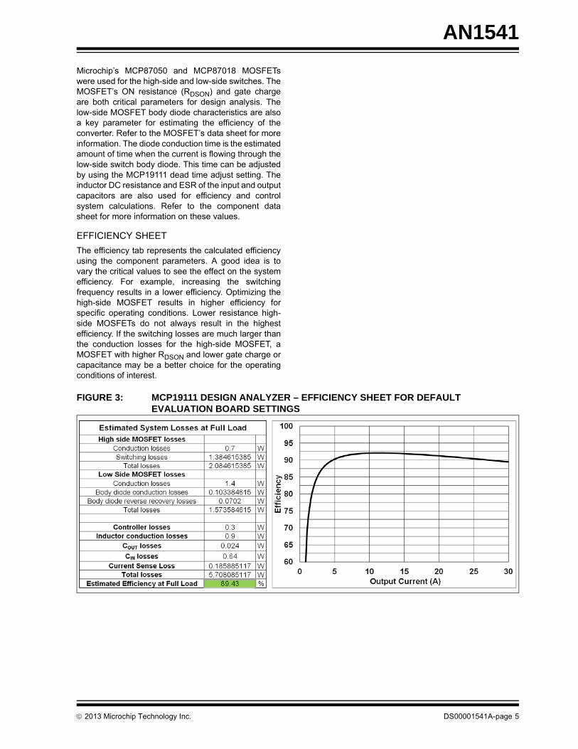
EFFICIENCY SHEET
The efficiency tab represents the calculated efficiencyusing the component parameters. A good idea is tovary the critical values to see the effect on the systemefficiency. For example, increasing the switchingfrequency results in a lower efficiency. Optimizing thehigh-side MOSFET results in higher efficiency forspecific operating conditions. Lower resistance high-side MOSFETs do not always result in the highestefficiency. If the switching losses are much larger thanthe conduction losses for the high-side MOSFET, aMOSFET with higher RDSON and lower gate charge orcapacitance may be a better choice for the operatingconditions of interest.
FIGURE 3: MCP19111 DESIGN ANALYZER – EFFICIENCY SHEET FOR DEFAULT EVALUATION BOARD SETTINGS
2013 Microchip Technology Inc. DS00001541A-page 5

AN1541
FREQUENCY ANALYSIS SHEET
This sheet shows the tools/elements that are used todesign the system's analog control loop. The cellsshaded green are the calculated values while thoseshaded yellow are filled in by the designer. The Gainand Zero Frequency cells from the Compensationsection set the position of the zero used to compensatethe control system. Changes in the system dynamicperformance result from changing the location of thesystem zero and gain. The next rows show the slopecompensation needed for peak current mode control.Adding more slope compensation makes the systemappear more voltage mode and can lead to instability(output voltage oscillation). The last two cells are usedto set the gain of the current sense signal.
The calculated system crossover frequency and phasemargin are also displayed. The higher the crossoverfrequency, the faster the system responds totransients. Higher switching frequency and lowerinductance enable a higher crossover frequency whilesacrificing efficiency. Phase margin greater than45 degrees is recommended.
FIGURE 4: MCP19111 DESIGN ANALYZER – CALCULATED BODE PLOT FOR DEFAULT EVALUATION BOARD SETTINGS
SPECIAL MACROS
There are two automated features in the MCP19111Design Analyzer that require the use of macros. TheUse Default Evaluation Board Compensation andComponents feature sets the designer cells (shadedyellow) to the default values that are standard on theMCP19111 Evaluation Board (ADM00397). Thisfeature is used as a reset to restore the analyzer backto the original evaluation board component values.
The Use Recommended Components andCompensation feature automatically fills in thedesigner input cells (shaded yellow) with the calculatedvalues. This feature is used to evaluate changes in keyparameters quickly (such as switching frequency,inductance, output capacitance and ESR, MOSFETparameters, etc.). Once the design goals are met, thedesigner can enter values in the input cells to furtheroptimize the size, efficiency and dynamic performance.
To access and use the macros, select “Developer” itemfrom the main menu/ribbon in Excel. In the “Code” sub-menu, click on the “Macros” icon. From the dialogwindow, select one of the available macros.
DS00001541A-page 6 2013 Microchip Technology Inc.

AN1541
GUI SHEET
The last step in the design phase is to review thecalculated GUI values in the design analyzer and enterthis data into the MCP19111 MPLAB® X IntegratedDevelopment Environment Plug-In. These values areprogrammed into the device.
FIGURE 5: MCP19111 DESIGN ANALYZER – GUI INPUTS FOR DEFAULT EVALUATION BOARD SETTINGS
Figure 5 shows three tables: Parameter, Protectionand Compensation. The Parameter table is used toset the output voltage and the mode of operation(single converter running stand alone, multi-outputconverter or multi-phase). The switching frequency,phase delay and maximum duty cycle define the pulse-width modulator (PWM) fixed frequency oscillator. TheDead Time Delay settings are used to adapt the delaybetween the high-side switch and low-side switchturning on and off. The value of 24 ns is set for theMicrochip MOSFETs. The settings used for the deadtime depend on the size and speed of the selectedMOSFETs. Microchip MOSFETs offer very lowcapacitance, resulting in faster switching times. Byusing a lower value delay, the system efficiency can beincreased using the Microchip MOSFETs. When usingtrench or MOSFETs with large gate capacitance, careshould be taken to ensure there is enough dead time.The last parameter in this tab specifies the rise time ofthe output voltage and the use of a GPIO pin for enable.
The Protection table is used for setting the outputovervoltage and undervoltage values. The MCP19111can detect if the output is ever outside of the expectedrange. The response options are provided in the GUI.In addition to the output overvoltage and undervoltagesettings, the input undervoltage lockout, startup voltageand high-side switch peak current limit can be adjustedto protect the power supply from abnormal operatingconditions.
The Compensation table is used to enter thecalculated parameters used to stabilize the system:
• Gain represents the amount of error amplifier gain added
• Zero Frequency is the location of where the control system Zero is placed
• Slope Amplitude and Slope dV/dT represent the amount of slope compensation added to the system (actually subtracted from the output of the error amplifier).
In the Current Sense Configuration section, there aretwo gain settings used to amplify the current sensesignal:
• Current Sense Gain - for AC
• Current Sense DC Gain - for DC
2013 Microchip Technology Inc. DS00001541A-page 7

AN1541
WORKING WITH MCP19111MPLAB® X IDE PLUG-IN
The next step in the design is to start the MPLAB® XIDE and run the MCP19111 plug-in. See “MCP19111MPLAB® X Integrated Development Environment Plug-in User’s Guide” for step-by-step instructions oninstalling and running the MCP19111 graphical userinterface (GUI).
Entering the Parameters into the MPLAB® X GUI Plug-In
The MCP19111 MPLAB X Integrated DevelopmentEnvironment Plug-In is used with the MPLAB X IDE toprogram the device for proper setup.
Figure 6 shows the MPLAB X IDE window. Once theMCP19111 Project is opened and the plug-in installed,the MPLAB X shows the plug-in panel under the projectwindow. The project tabs inputs (Parameter,Protection and Compensation) match the MCP19111Design Analyzer’s GUI sheet. The output values fromthe analyzer are manually entered into the MPLAB XGUI.
PARAMETER TAB
Figure 6 depicts the Parameter tab with the parametervalues filled in from the design analyzer spreadsheetGUI page.
FIGURE 6: MPLAB® X IDE – PARAMETER TAB WITH DEFAULT EVALUATION BOARD SETTINGS COMPLETED
MCP19111 Project Parameter tab
DS00001541A-page 8 2013 Microchip Technology Inc.
AN1541
PROTECTION TAB
Figure 7 shows the Protection tab filled in with thevalues from the MCP19111 Design Analyzer.
FIGURE 7: MPLAB® X IDE – PROTECTION TAB WITH DEFAULT EVALUATION BOARD SETTINGS COMPLETED
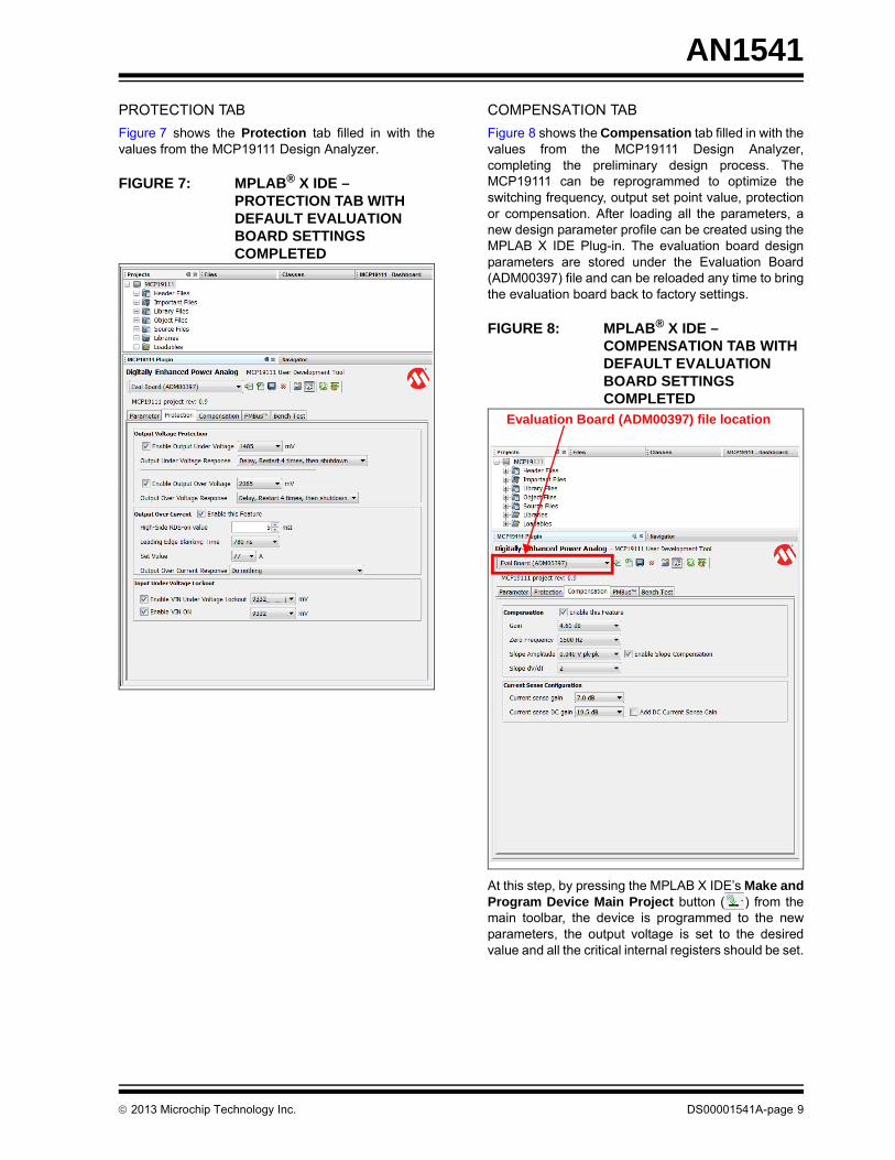
COMPENSATION TAB
Figure 8 shows the Compensation tab filled in with thevalues from the MCP19111 Design Analyzer,completing the preliminary design process. TheMCP19111 can be reprogrammed to optimize theswitching frequency, output set point value, protectionor compensation. After loading all the parameters, anew design parameter profile can be created using theMPLAB X IDE Plug-in. The evaluation board designparameters are stored under the Evaluation Board(ADM00397) file and can be reloaded any time to bringthe evaluation board back to factory settings.
FIGURE 8: MPLAB® X IDE – COMPENSATION TAB WITH DEFAULT EVALUATION BOARD SETTINGS COMPLETED
At this step, by pressing the MPLAB X IDE’s Make andProgram Device Main Project button ( ) from themain toolbar, the device is programmed to the newparameters, the output voltage is set to the desiredvalue and all the critical internal registers should be set.
Evaluation Board (ADM00397) file location
2013 Microchip Technology Inc. DS00001541A-page 9

AN1541
MCP19111 EVALUATION BOARD (ADM00397) MEASUREMENTS
Figure 9 through Figure 13 represents the actual datataken from a standard MCP19111 Evaluation Board(ADM00397) while using the default settings(ADM00397) from the GUI sheet.
Figure 9 shows the efficiency of the Evaluation Boardwhile operating with the chosen optimized dead timevs. non-optimized dead time.
FIGURE 9: EFFICIENCY VS. OUTPUT CURRENT AT 12V INPUT, 1.8V OUTPUT
Figure 10 represents the system efficiency vs. load,using the selected 1.8 m low-side FET compared to a2.2 m low-side FET.
FIGURE 10: EFFICIENCY VS. OUTPUT CURRENT AT 12V INPUT, 1.8V OUTPUT
Figure 11 represents the measured system bode plot incomparison to the calculated system bode plot whenusing the calculated values.
FIGURE 11: MEASURED BODE PLOT PERFORMANCE
Figure 12 shows the system response to a load step,top traces representing a high-to-low load step, whilethe bottom traces represent a low-to-high step.
FIGURE 12: STEP LOAD RESPONSE
Figure 13 shows steady state waveforms with a 20Aload. The top trace displays the inductor current, whilethe bottom two traces show the gate drive outputs fromthe MCP19111.
FIGURE 13: SWITCHING WAVEFORMS AT 30A LOAD
0.8
0.85
0.9
0.95
Effic
ienc
y
1.8 mΩ Efficiency vs. IOUT
Optimized Dead Time
non-Optimized Dead Time
0.65
0.7
0.75
0 10 20 30
E
Output Current (A)
0.8
0.85
0.9
0.95
Effic
ienc
y
1.8 mΩ and 2.2 mΩ Low-Side FET Efficiency vs. IOUT
1.8 mΩ
2.2 mΩ
0.65
0.7
0.75
0 10 20 30Output Current (A)
VOUT 50 mV/div
IOUT 5 A/div
VOUT 50 mV/div
IOUT 5 A/div
AC Coupled
50 µs/div
AC Coupled
50 µs/div
LDRV 5 V/div
IL 10 A/div
HDRV 5 V/div2 µs/div
DS00001541A-page 10 2013 Microchip Technology Inc.

AN1541
CONCLUSION
The MCP19111 device integrates aPIC microcontroller, flash memory, high voltage, highcurrent half-bridge driver and precise analogtechnology into one monolithic device. This applicationnote covered the design tools used to quickly scale aPoint-of-Load design. The MCP19111 can be used fordeveloping power systems to drive LEDs, chargebatteries or produce general purpose DC-DCconverters. The integrated analog control systemallows the designer to adapt and adjust the dynamicperformance without printed circuit board changeswhile only consuming 5 mA of the input current. Specialfeatures for increasing efficiency, dynamicperformance and the ability to communicate make theMCP19111 a good choice for many new applicationsand designs.
2013 Microchip Technology Inc. DS00001541A-page 11

AN1541
APPENDIX A: MCP19111 DESIGN ANALYZER TOOL
This appendix reviews some of the design tool’scharacteristics and shows the equations used to plotthe estimated efficiency and bode response.
TABLE A-1: RECOMMENDED PARAMETERS CALCULATION - INPUT PARAMETERS SHEET
Parameter Equation
• All values are user input.
• The user must enter values within the specified range given in the “Notes” column. An error occurs if a value outside of this range is used.
TABLE A-2: RECOMMENDED PARAMETERS CALCULATION - COMPONENTS SHEET
Parameter Equation
Recommended Inductance
Recommended Output Capacitance
Recommended Input Capacitance
Recommended Sense Filter Resistor
Recommended Sense Filter Capacitor
This value is fixed at 100 nF
Power Train Components All parameters are selected by user
L VIN VOUT– VOUT
VIN------------- T
10.2 IOUT--------------------------=
This is calculated based on a 20% ripple current.
COUT
L IOH2
IOL2–
VOUT VOVERSHOOT+ 2 VOUT2–
-------------------------------------------------------------------------------------=
CIN
IOUT D 1 D– fSW VRIPPLE D IOUT CINESR
– ------------------------------------------------------------------------------------------------=
RfL
10 LDCR Cf-------------------------------------=
DS00001541A-page 12 2013 Microchip Technology Inc.

AN1541
2013 Microchip Technology Inc. DS00001541A-page 13
TABLE A-3: RECOMMENDED PARAMETERS CALCULATION - EFFICIENCY SHEET
Device Type Parameter Equation
High-Side MOSFET
Conduction Losses
Switching Losses
Low-Side MOSFET
Conduction Losses
Body Diode Conduction Losses
Body Diode Reverse Recovery Losses
Controller Losses
Inductor Conduction Losses
COUT Losses
CIN Losses
PCONDHSIRMSHS
2RDSHS
=
PSWHSVIN IOUT QGATEHS fSW=
PCONDLSIRMSLS
2RDSLS
=
PLOSSBDIOUT Vf tBD fSW=
PLOSSRR
QRR VIN fSW2----------------------------------------=
PLOSSCONTVIN 5mA fSW QGATELOW
QGATEHIGH+ + =
PLOSSINDILRMS2
LDCR=
PLOSSOUTCOUTESR
0.2IOUT
3------------=
PLOSSCINCINESR
IRMSHS
VOUT IOUTVIN
--------------------------------–
2=
AN1541
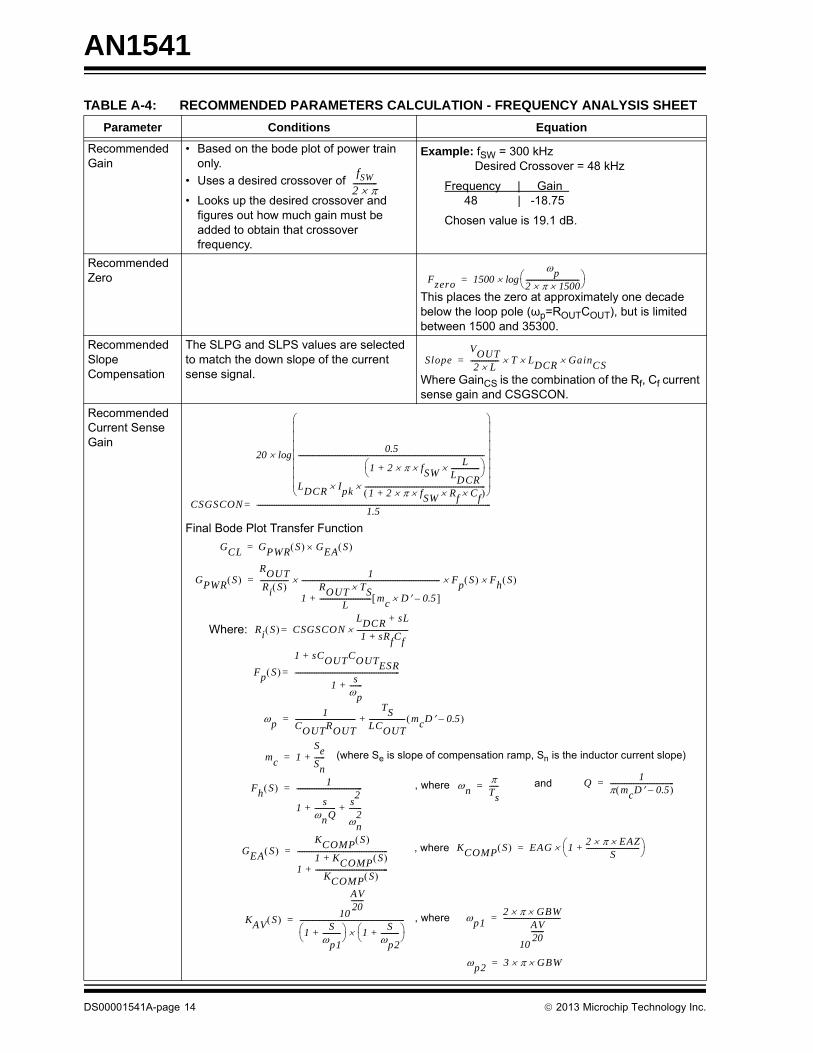
TABLE A-4: RECOMMENDED PARAMETERS CALCULATION - FREQUENCY ANALYSIS SHEET
Parameter Conditions Equation
Recommended Gain
• Based on the bode plot of power train only.
• Uses a desired crossover of
• Looks up the desired crossover and figures out how much gain must be added to obtain that crossover frequency.
Example: fSW = 300 kHzDesired Crossover = 48 kHz
Frequency | Gain 48 | -18.75
Chosen value is 19.1 dB.
Recommended Zero
This places the zero at approximately one decade below the loop pole (ωp=ROUTCOUT), but is limited between 1500 and 35300.
Recommended Slope Compensation
The SLPG and SLPS values are selected to match the down slope of the current sense signal. Where GainCS is the combination of the Rf, Cf current
sense gain and CSGSCON.
Recommended Current Sense Gain
Final Bode Plot Transfer Function
fSW
2 ------------
Fzero 1500p
2 1500------------------------------ log=
SlopeVOUT2 L
---------------- T LDCR GainCS=
CSGSCON
200.5
LDCR Ipk
1 2 fSWL
LDCR----------------+
1 2 fSW Rf Cf+ --------------------------------------------------------------------
---------------------------------------------------------------------------------------------------------
log
1.5------------------------------------------------------------------------------------------------------------------------------------=
GCL GPWR S GEA S =
GPWR S ROUTRi S ----------------
1
1ROUT TS
L----------------------------- mc D 0.5– +
------------------------------------------------------------------------------ Fp S Fh S =
Where: Ri S CSGSCONLDCR sL+
1 sRfCf+-----------------------------=
Fp S
1 sCOUTCOUTESR+
1sp-------+
-----------------------------------------------------------=
p1
COUTROUT----------------------------------
TSLCOUT-------------------- mcD 0.5– +=
mc 1SeSn------+= (where Se is slope of compensation ramp, Sn is the inductor current slope)
Fh S 1
1s
nQ------------
s2
n2
-------+ +
-------------------------------------= nTs-----= Q
1 mcD 0.5– ------------------------------------=, where and
GEA S KCOMP S
11 KCOMP S +
KCOMP S -----------------------------------------+
---------------------------------------------------= KCOMP S EAG 12 EAZ
S------------------------------+
=
KAV S 10
AV20-------
1S
p1----------+
1S
p2----------+
-----------------------------------------------------------= p1
2 GBW
10
AV20-------
--------------------------------=
p2 3 GBW=
, where
, where
DS00001541A-page 14 2013 Microchip Technology Inc.
AN1541
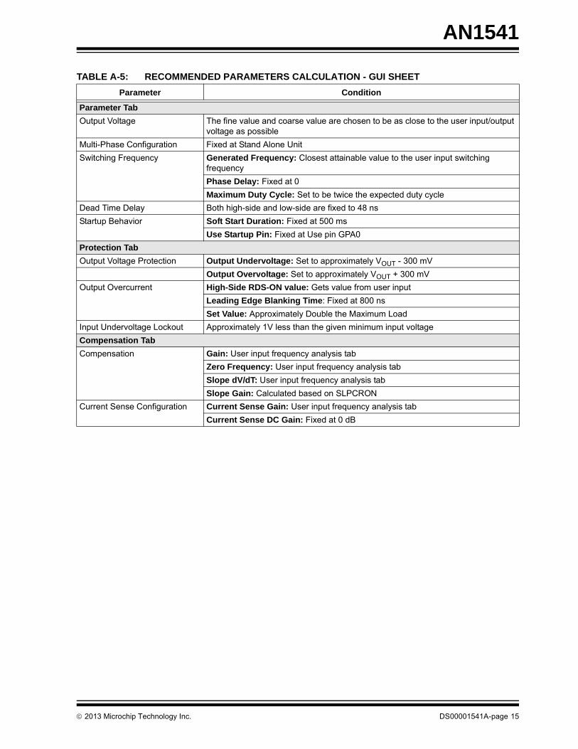
TABLE A-5: RECOMMENDED PARAMETERS CALCULATION - GUI SHEET
Parameter Condition
Parameter Tab
Output Voltage The fine value and coarse value are chosen to be as close to the user input/output voltage as possible
Multi-Phase Configuration Fixed at Stand Alone Unit
Switching Frequency Generated Frequency: Closest attainable value to the user input switching frequency
Phase Delay: Fixed at 0
Maximum Duty Cycle: Set to be twice the expected duty cycle
Dead Time Delay Both high-side and low-side are fixed to 48 ns
Startup Behavior Soft Start Duration: Fixed at 500 ms
Use Startup Pin: Fixed at Use pin GPA0
Protection Tab
Output Voltage Protection Output Undervoltage: Set to approximately VOUT - 300 mV
Output Overvoltage: Set to approximately VOUT + 300 mV
Output Overcurrent High-Side RDS-ON value: Gets value from user input
Leading Edge Blanking Time: Fixed at 800 ns
Set Value: Approximately Double the Maximum Load
Input Undervoltage Lockout Approximately 1V less than the given minimum input voltage
Compensation Tab
Compensation Gain: User input frequency analysis tab
Zero Frequency: User input frequency analysis tab
Slope dV/dT: User input frequency analysis tab
Slope Gain: Calculated based on SLPCRON
Current Sense Configuration Current Sense Gain: User input frequency analysis tab
Current Sense DC Gain: Fixed at 0 dB
2013 Microchip Technology Inc. DS00001541A-page 15

AN1541
NOTES:
DS00001541A-page 16 2013 Microchip Technology Inc.
Note the following details of the code protection feature on Microchip devices:
• Microchip products meet the specification contained in their particular Microchip Data Sheet.
• Microchip believes that its family of products is one of the most secure families of its kind on the market today, when used in the intended manner and under normal conditions.
• There are dishonest and possibly illegal methods used to breach the code protection feature. All of these methods, to our knowledge, require using the Microchip products in a manner outside the operating specifications contained in Microchip’s Data Sheets. Most likely, the person doing so is engaged in theft of intellectual property.
• Microchip is willing to work with the customer who is concerned about the integrity of their code.
• Neither Microchip nor any other semiconductor manufacturer can guarantee the security of their code. Code protection does not mean that we are guaranteeing the product as “unbreakable.”
Code protection is constantly evolving. We at Microchip are committed to continuously improving the code protection features of ourproducts. Attempts to break Microchip’s code protection feature may be a violation of the Digital Millennium Copyright Act. If such actsallow unauthorized access to your software or other copyrighted work, you may have a right to sue for relief under that Act.
Information contained in this publication regarding deviceapplications and the like is provided only for your convenienceand may be superseded by updates. It is your responsibility toensure that your application meets with your specifications.MICROCHIP MAKES NO REPRESENTATIONS ORWARRANTIES OF ANY KIND WHETHER EXPRESS ORIMPLIED, WRITTEN OR ORAL, STATUTORY OROTHERWISE, RELATED TO THE INFORMATION,INCLUDING BUT NOT LIMITED TO ITS CONDITION,QUALITY, PERFORMANCE, MERCHANTABILITY ORFITNESS FOR PURPOSE. Microchip disclaims all liabilityarising from this information and its use. Use of Microchipdevices in life support and/or safety applications is entirely atthe buyer’s risk, and the buyer agrees to defend, indemnify andhold harmless Microchip from any and all damages, claims,suits, or expenses resulting from such use. No licenses areconveyed, implicitly or otherwise, under any Microchipintellectual property rights.
2013 Microchip Technology Inc.
QUALITY MANAGEMENT SYSTEM CERTIFIED BY DNV
== ISO/TS 16949 ==
Trademarks
The Microchip name and logo, the Microchip logo, dsPIC, FlashFlex, KEELOQ, KEELOQ logo, MPLAB, PIC, PICmicro, PICSTART, PIC32 logo, rfPIC, SST, SST Logo, SuperFlash and UNI/O are registered trademarks of Microchip Technology Incorporated in the U.S.A. and other countries.
FilterLab, Hampshire, HI-TECH C, Linear Active Thermistor, MTP, SEEVAL and The Embedded Control Solutions Company are registered trademarks of Microchip Technology Incorporated in the U.S.A.
Silicon Storage Technology is a registered trademark of Microchip Technology Inc. in other countries.
Analog-for-the-Digital Age, Application Maestro, BodyCom, chipKIT, chipKIT logo, CodeGuard, dsPICDEM, dsPICDEM.net, dsPICworks, dsSPEAK, ECAN, ECONOMONITOR, FanSense, HI-TIDE, In-Circuit Serial Programming, ICSP, Mindi, MiWi, MPASM, MPF, MPLAB Certified logo, MPLIB, MPLINK, mTouch, Omniscient Code Generation, PICC, PICC-18, PICDEM, PICDEM.net, PICkit, PICtail, REAL ICE, rfLAB, Select Mode, SQI, Serial Quad I/O, Total Endurance, TSHARC, UniWinDriver, WiperLock, ZENA and Z-Scale are trademarks of Microchip Technology Incorporated in the U.S.A. and other countries.
SQTP is a service mark of Microchip Technology Incorporated in the U.S.A.
GestIC and ULPP are registered trademarks of Microchip Technology Germany II GmbH & Co. KG, a subsidiary of Microchip Technology Inc., in other countries.
All other trademarks mentioned herein are property of their respective companies.
© 2013, Microchip Technology Incorporated, Printed in the U.S.A., All Rights Reserved.
Printed on recycled paper.
ISBN: 978-1-62077-355-0
Microchip received ISO/TS-16949:2009 certification for its worldwide
DS00001541A-page 17
headquarters, design and wafer fabrication facilities in Chandler and Tempe, Arizona; Gresham, Oregon and design centers in California and India. The Company’s quality system processes and procedures are for its PIC® MCUs and dsPIC® DSCs, KEELOQ® code hopping devices, Serial EEPROMs, microperipherals, nonvolatile memory and analog products. In addition, Microchip’s quality system for the design and manufacture of development systems is ISO 9001:2000 certified.
DS00001541A-page 18 2013 Microchip Technology Inc.
AMERICASCorporate Office2355 West Chandler Blvd.Chandler, AZ 85224-6199Tel: 480-792-7200 Fax: 480-792-7277Technical Support: http://www.microchip.com/supportWeb Address: www.microchip.com
AtlantaDuluth, GA Tel: 678-957-9614 Fax: 678-957-1455
BostonWestborough, MA Tel: 774-760-0087 Fax: 774-760-0088
ChicagoItasca, IL Tel: 630-285-0071 Fax: 630-285-0075
ClevelandIndependence, OH Tel: 216-447-0464 Fax: 216-447-0643
DallasAddison, TX Tel: 972-818-7423 Fax: 972-818-2924
DetroitFarmington Hills, MI Tel: 248-538-2250Fax: 248-538-2260
IndianapolisNoblesville, IN Tel: 317-773-8323Fax: 317-773-5453
Los AngelesMission Viejo, CA Tel: 949-462-9523 Fax: 949-462-9608
Santa ClaraSanta Clara, CA Tel: 408-961-6444Fax: 408-961-6445
TorontoMississauga, Ontario, CanadaTel: 905-673-0699 Fax: 905-673-6509
ASIA/PACIFICAsia Pacific OfficeSuites 3707-14, 37th FloorTower 6, The GatewayHarbour City, KowloonHong KongTel: 852-2401-1200Fax: 852-2401-3431
Australia - SydneyTel: 61-2-9868-6733Fax: 61-2-9868-6755
China - BeijingTel: 86-10-8569-7000 Fax: 86-10-8528-2104
China - ChengduTel: 86-28-8665-5511Fax: 86-28-8665-7889
China - ChongqingTel: 86-23-8980-9588Fax: 86-23-8980-9500
China - HangzhouTel: 86-571-2819-3187 Fax: 86-571-2819-3189
China - Hong Kong SARTel: 852-2943-5100 Fax: 852-2401-3431
China - NanjingTel: 86-25-8473-2460Fax: 86-25-8473-2470
China - QingdaoTel: 86-532-8502-7355Fax: 86-532-8502-7205
China - ShanghaiTel: 86-21-5407-5533 Fax: 86-21-5407-5066
China - ShenyangTel: 86-24-2334-2829Fax: 86-24-2334-2393
China - ShenzhenTel: 86-755-8864-2200 Fax: 86-755-8203-1760
China - WuhanTel: 86-27-5980-5300Fax: 86-27-5980-5118
China - XianTel: 86-29-8833-7252Fax: 86-29-8833-7256
China - XiamenTel: 86-592-2388138 Fax: 86-592-2388130
China - ZhuhaiTel: 86-756-3210040 Fax: 86-756-3210049
ASIA/PACIFICIndia - BangaloreTel: 91-80-3090-4444 Fax: 91-80-3090-4123
India - New DelhiTel: 91-11-4160-8631Fax: 91-11-4160-8632
India - PuneTel: 91-20-3019-1500
Japan - OsakaTel: 81-6-6152-7160 Fax: 81-6-6152-9310
Japan - TokyoTel: 81-3-6880- 3770 Fax: 81-3-6880-3771
Korea - DaeguTel: 82-53-744-4301Fax: 82-53-744-4302
Korea - SeoulTel: 82-2-554-7200Fax: 82-2-558-5932 or 82-2-558-5934
Malaysia - Kuala LumpurTel: 60-3-6201-9857Fax: 60-3-6201-9859
Malaysia - PenangTel: 60-4-227-8870Fax: 60-4-227-4068
Philippines - ManilaTel: 63-2-634-9065Fax: 63-2-634-9069
SingaporeTel: 65-6334-8870Fax: 65-6334-8850
Taiwan - Hsin ChuTel: 886-3-5778-366Fax: 886-3-5770-955
Taiwan - KaohsiungTel: 886-7-213-7828Fax: 886-7-330-9305
Taiwan - TaipeiTel: 886-2-2508-8600 Fax: 886-2-2508-0102
Thailand - BangkokTel: 66-2-694-1351Fax: 66-2-694-1350
EUROPEAustria - WelsTel: 43-7242-2244-39Fax: 43-7242-2244-393Denmark - CopenhagenTel: 45-4450-2828 Fax: 45-4485-2829
France - ParisTel: 33-1-69-53-63-20 Fax: 33-1-69-30-90-79
Germany - MunichTel: 49-89-627-144-0 Fax: 49-89-627-144-44
Italy - Milan Tel: 39-0331-742611 Fax: 39-0331-466781
Netherlands - DrunenTel: 31-416-690399 Fax: 31-416-690340
Spain - MadridTel: 34-91-708-08-90Fax: 34-91-708-08-91
UK - WokinghamTel: 44-118-921-5869Fax: 44-118-921-5820
Worldwide Sales and Service
08/20/13