An Update on AIM Photonics - SPIE
48
An Update on AIM Photonics November 17, 2015
Transcript of An Update on AIM Photonics - SPIE

An Update on AIM PhotonicsNovember 17, 2015
An Update on AIM PhotonicsNovember 17, 2015
Welcome
Dr. Alan Willner
Chair
NPI Steering Committee
Agenda
Welcome & Introduction: Dr. Alan Willner, chair, NPI Steering Committee
AIM Photonics Update: Dr. Thomas L. Koch, chair, Technical Review Board, AIM Photonics
Closing Remarks: Dr. Tom Baer, past chair, NPI Steering Committee
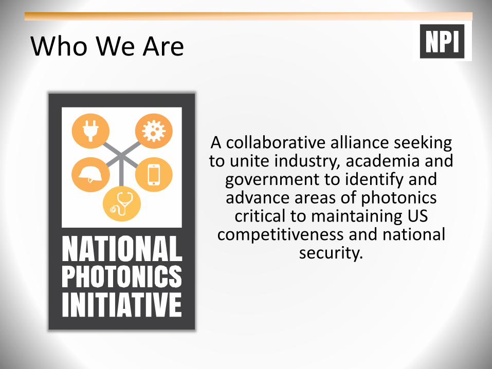
Who We Are
A collaborative alliance seeking to unite industry, academia and
government to identify and advance areas of photonics
critical to maintaining US competitiveness and national
security.
Partners
Sponsors:
Founding Sponsors:
Collaborators & Supporters
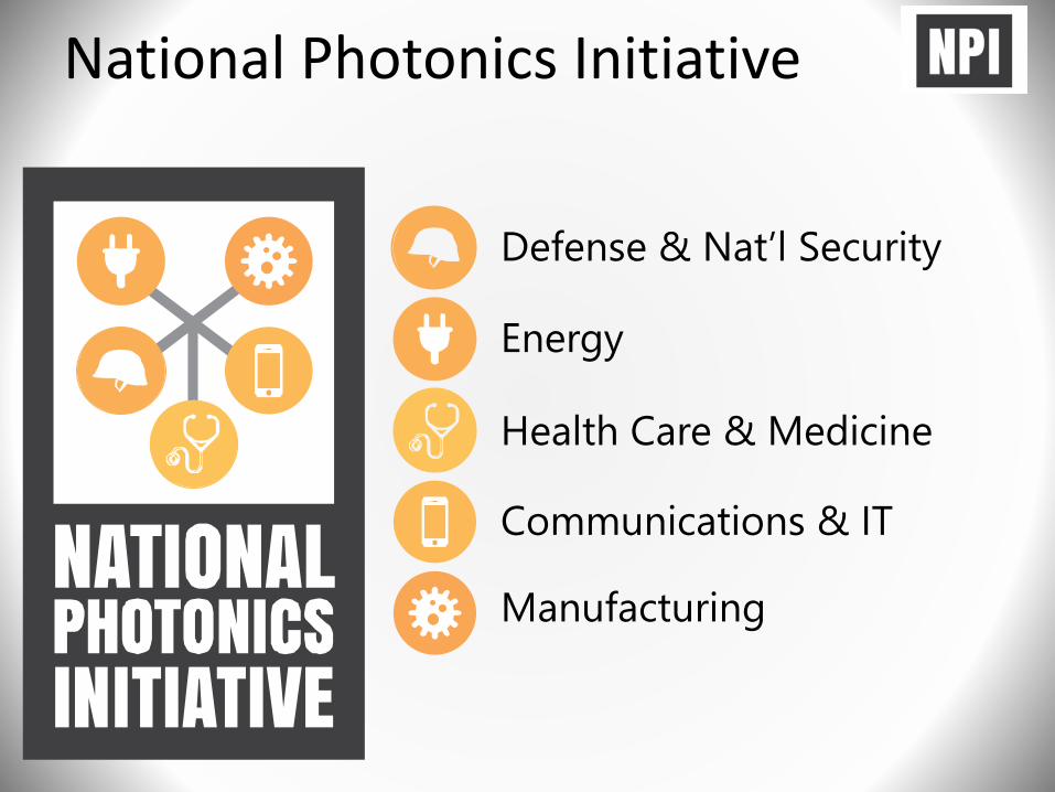
National Photonics Initiative
Defense & Nat’l Security
Energy
Health Care & Medicine
Communications & IT
Manufacturing
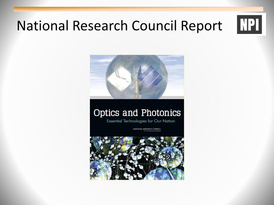
National Research Council Report

NPI Advocacy Strategy
• Educate members of Congress
• Build champions
• Collaborate with the Administration
• Secure legislative language & funding
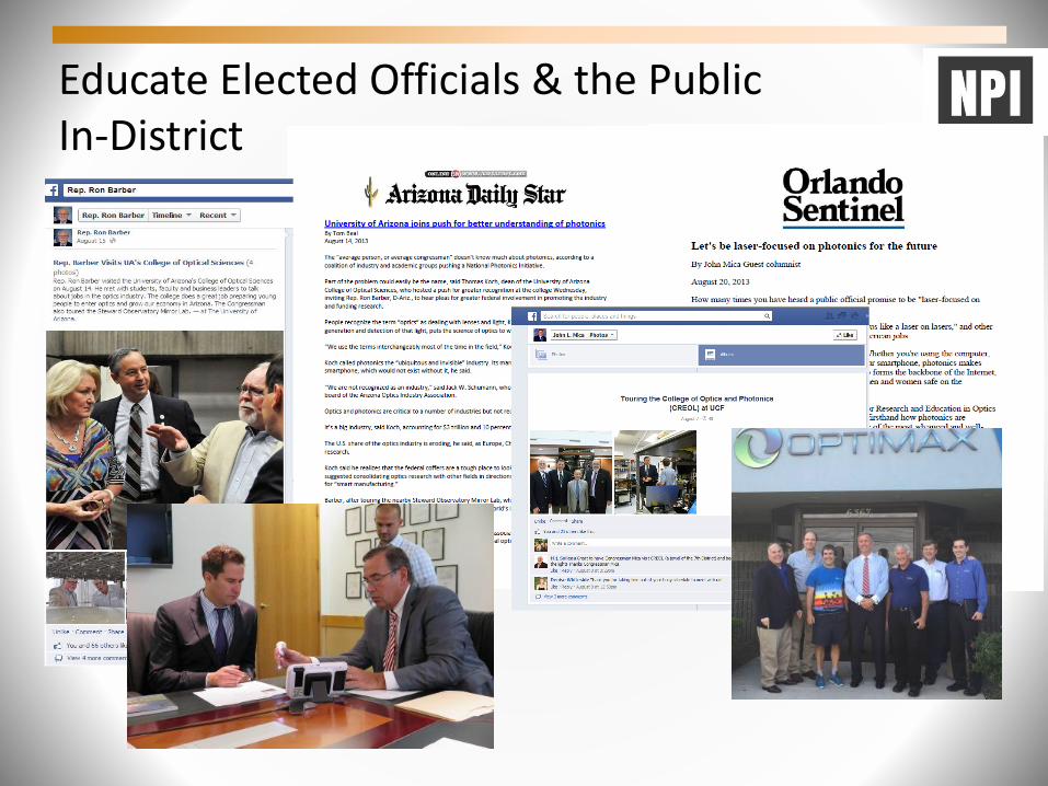
Educate Elected Officials & the Public In-District
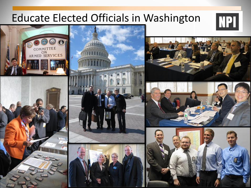
Educate Elected Officials in Washington
NPI Greatest Successes: Congressional
• Secured optics and photonics report language in the National Defense Authorization Act (NDAA) for FY 2015
• Secured optics and photonics language in the Senate-introduced America COMPETES Reauthorization Act of 2014
• Supported optics and photonics language in the House-passed Reinvesting in American Manufacturing Innovation (RAMI) Act, which was included in the FY2015 omnibus bill
• Hosted numerous fly-ins, in-district visits and congressional meetings to demonstrate constituent support for NPI priorities in Congress and optics and photonics policy leadership: COMPETES, RAMI, NDAA, ITAR, Higher Education Act
NPI Greatest Successes:Administration
• Advanced Manufacturing: Mobilized and led photonics community to support and secure presidential endorsement for a DOD-led Integrated Photonics Institute for Manufacturing Innovation (IP-IMI).
• Health Care and Medicine: Created and launched the NPI Photonics Industry Neuroscience Group (PING) alongside White House and federal agency officials in support of BRAIN Initiative Grand Challenge; developed and published first-of-its-kind optics and photonics technology road map for White House and program managers across five agencies.
• IT and Communications: Secured seat at White House policymaking table to ensure optics and photonics are part of next generation High Performance Computing architectures.

NPI’s Role in the IP-IMI Process
• Submitted a white paper to White House Office of Science and Technology Policy (OSTP) staff recommending a photonics prototyping and advanced manufacturing facility; opened the door to conversations between the NPI and DOD, and aided in the national push for a photonics IMI.
• Hosted webinars with DOD officials to educate the photonics community about the selection process.
• Coordinated responses to the FOA from dozens of experts, and matched industry with academia to submit proposals.
• Provided regular communication to the community as to relevant deadlines and information.
• Upon request, supplied a letter of support to include in proposal submissions.
• Engaged the media around the IP-IMI announcement.
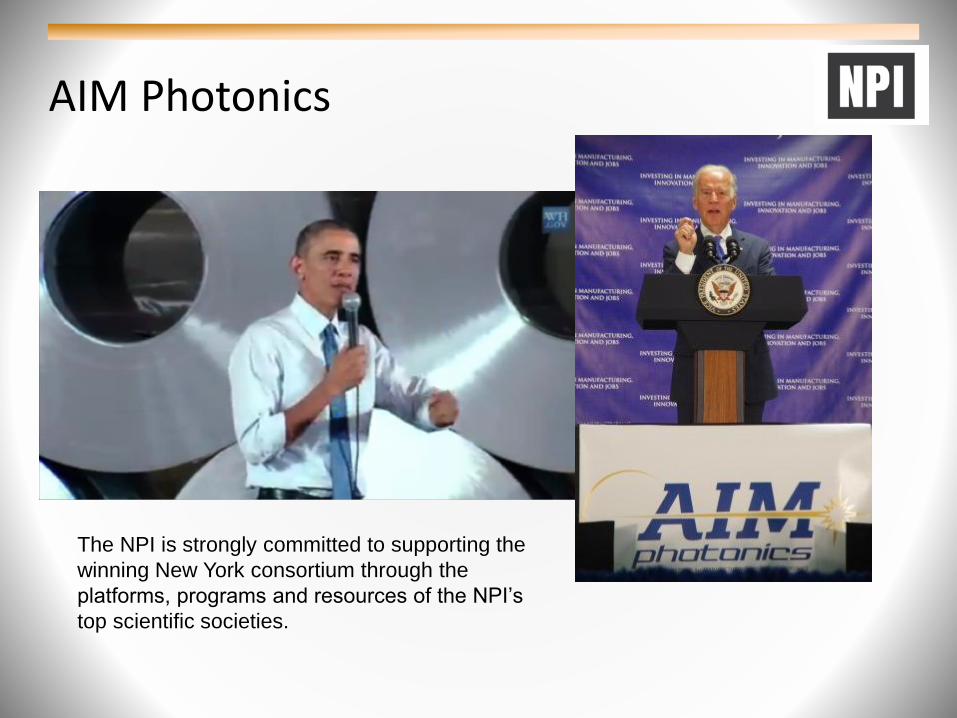
AIM Photonics
The NPI is strongly committed to supporting the
winning New York consortium through the
platforms, programs and resources of the NPI’s
top scientific societies.

AIM Photonics Update
Dr. Thomas L. Koch, chair, Technical Review Board, AIM Photonics
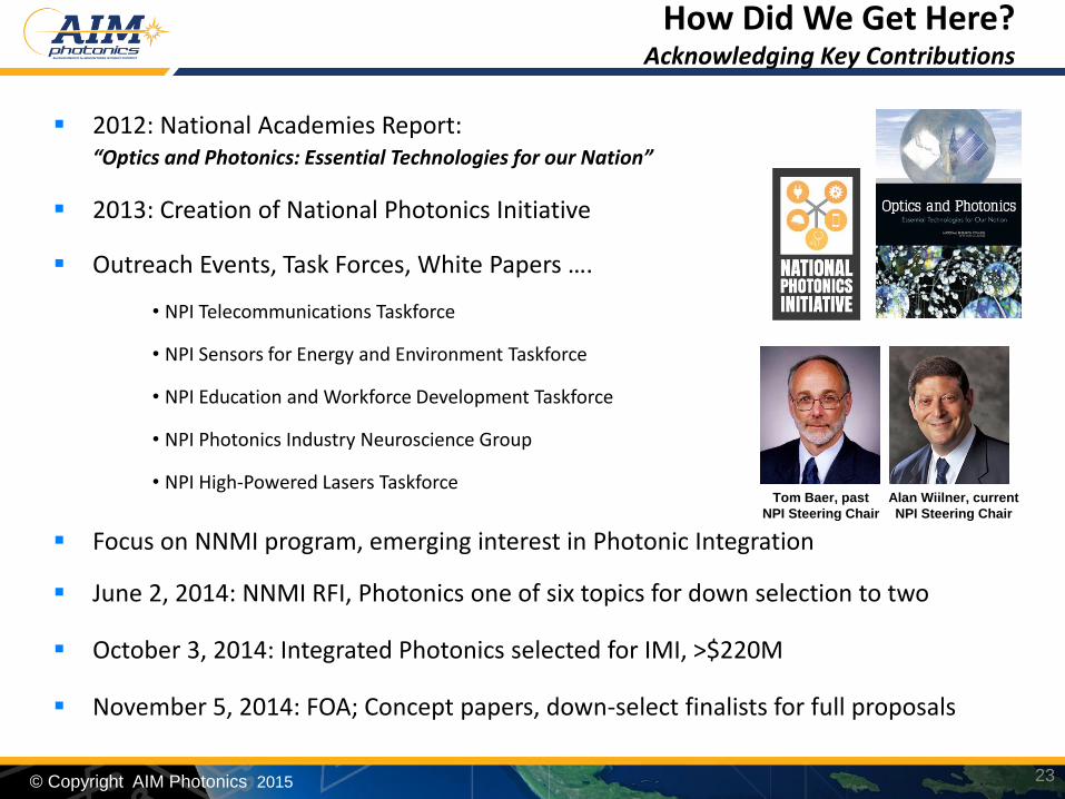
How Did We Get Here?Acknowledging Key Contributions
2012: National Academies Report:“Optics and Photonics: Essential Technologies for our Nation”
2013: Creation of National Photonics Initiative
Outreach Events, Task Forces, White Papers ….
Focus on NNMI program, emerging interest in Photonic Integration
June 2, 2014: NNMI RFI, Photonics one of six topics for down selection to two
October 3, 2014: Integrated Photonics selected for IMI, >$220M
November 5, 2014: FOA; Concept papers, down-select finalists for full proposals
23
• NPI Telecommunications Taskforce
• NPI Sensors for Energy and Environment Taskforce
• NPI Education and Workforce Development Taskforce
• NPI Photonics Industry Neuroscience Group
• NPI High-Powered Lasers TaskforceTom Baer, past
NPI Steering Chair
Alan Wiilner, current
NPI Steering Chair
© Copyright AIM Photonics 2015

AIM Photonics Launch – July 27, 2015, Rochester, NY
US VICE PRESIDENT JOE BIDEN (CENTER) MEETS SUNY POLYTECHNIC INSTITUTE'S FOUNDING PRESIDENT AND CEO DR. ALAIN KALOYEROS (FAR LEFT) AND NEW YORK STATE GOVERNOR ANDREW CUOMO (RIGHT OF CENTER) DURING THE OFFICIAL ANNOUNCEMENT OF THE AIM PHOTONICS HUB IN ROCHESTER, NY, ON JULY 27, 2015.
24
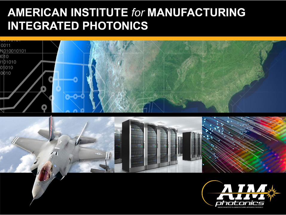
• American Institute for Manufacturing Integrated Photonics (AIM Photonics)
• Sixth Institute in National Network of Manufacturing Innovation (NNMI) program.
• Largest institute to date, with $110M of federal funding and more than $500M of matching funding from state, industry, and academic partners
© Copyright AIM Photonics 2015

Core Integrated Photonics Fab Facility
SUNY Poly Albany NanoTech Complex – Albany, NY:• 1.3 million Sq. Ft. facility with 300 and 450mm
toolsets • 135,000 Sq. Ft. of class 10K and better cleanroom• Wet labs, metrology labs and 3D packaging• 65nm low power CMOS base line; 7nm CMOS
capable• Leading edge lithography and dedicated eng. staff• Multiple prior photonics DARPA projects
• Years of proven results in Si photonics• 300mm wafer tools provide
unprecedented quality photonics• Sematech partnerships drive
continued investment to remain at state-of-the-art
• 3D stacking w/CMOS
© Copyright AIM Photonics 2015
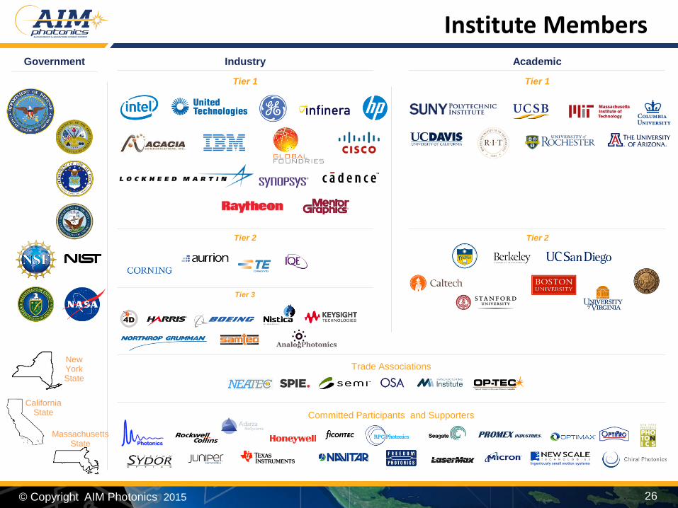
Industry AcademicGovernment
Tier 1 Tier 1
Tier 2 Tier 2
Tier 3
Trade Associations
Committed Participants and Supporters
26
New York State
California State
Massachusetts State
Institute Members
© Copyright AIM Photonics 2015
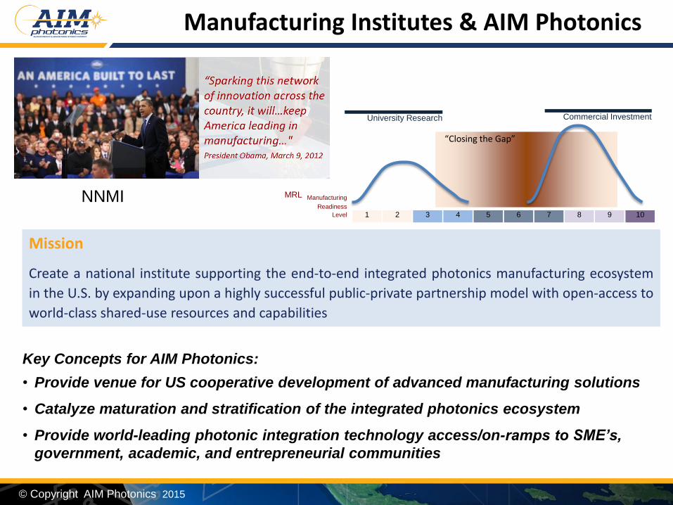
Manufacturing Institutes & AIM Photonics
Mission
Create a national institute supporting the end-to-end integrated photonics manufacturing ecosystem
in the U.S. by expanding upon a highly successful public-private partnership model with open-access to
world-class shared-use resources and capabilities
MRL Manufacturing
Readiness
Level
Commercial Investment
“Closing the Gap”
1 2 3 4 5 6 7 8 9 10
University Research
Key Concepts for AIM Photonics:
• Provide venue for US cooperative development of advanced manufacturing solutions
• Catalyze maturation and stratification of the integrated photonics ecosystem
• Provide world-leading photonic integration technology access/on-ramps to SME’s,
government, academic, and entrepreneurial communities
NNMI
© Copyright AIM Photonics 2015
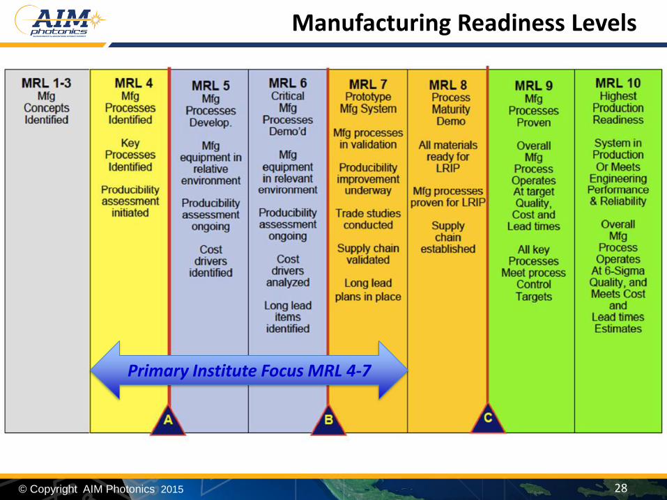
Manufacturing Readiness Levels
28
Primary Institute Focus MRL 4-7
© Copyright AIM Photonics 2015
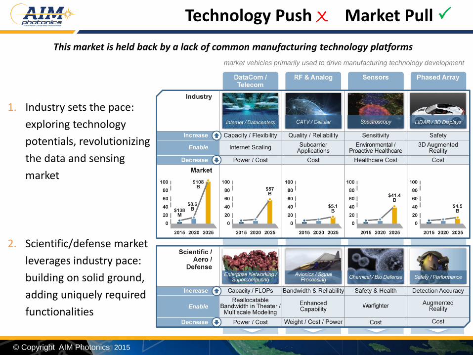
This market is held back by a lack of common manufacturing technology platforms
1. Industry sets the pace:
exploring technology
potentials, revolutionizing
the data and sensing
market
2. Scientific/defense market
leverages industry pace:
building on solid ground,
adding uniquely required
functionalities
market vehicles primarily used to drive manufacturing technology development
Technology Push X Market Pull
© Copyright AIM Photonics 2015
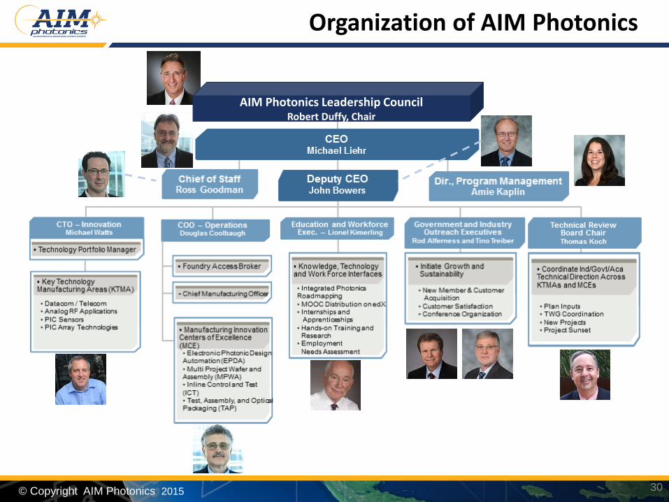
Organization of AIM Photonics
30
AIM Photonics Leadership CouncilRobert Duffy, Chair
© Copyright AIM Photonics 2015

Electronic & Photonic Design
Automation (EPDA)
Inline Control & Test (ICT)
Test, Assembly & Packaging (TAP)
MultiProject Wafer & Assembly (MPWA)
PI &
PM
TWG
PI &
PM
TWG
PI &
PM
TWG
PI &
PM
TWG
Man
ufa
ctu
rin
g C
apab
ility
&D
esig
n P
latf
orm
Ro
adm
aps
Manufacturing innovationCenters of Excellent (MCEs)
31
Matrix Institute Business Operations – MCEs
Role of Manufacturing innovation Centers of Excellence (MCEs):
• Function like manufacturing & design platforms in a corporation
• Drive stratification/maturation of photonic integration industry ecosystem
• Provide baseline capabilities in each manufacturing support area (i.e., for foundry services)
• Use Technical Working Groups (TWGs) comprised of institute partners for inputs & project proposals
• Select projects that maximize synergy across KTMAs and advance AIM Photonics manufacturing capacity
• Each MCE has industry, government, and academic co-leads
© Copyright AIM Photonics 2015
An
alo
g an
d R
F C
om
mu
nic
atio
ns
Inte
grat
ed P
ho
ton
ic
Sen
sors
PIC
Arr
ay
Tech
no
logi
es
VH
S D
igit
al D
ata
and
C
om
m.
Lin
ks
TWG
PI &PM
TWG
PI &PM
TWG
PI &PM
TWG
PI &PM
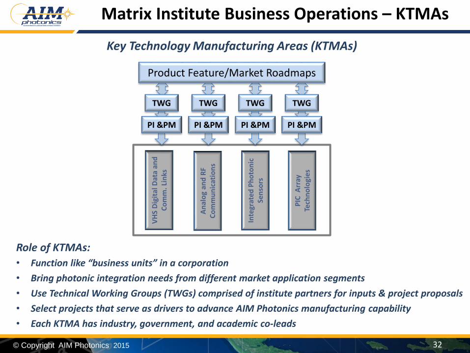
Product Feature/Market Roadmaps
Key Technology Manufacturing Areas (KTMAs)
32
Matrix Institute Business Operations – KTMAs
Role of KTMAs:
• Function like “business units” in a corporation
• Bring photonic integration needs from different market application segments
• Use Technical Working Groups (TWGs) comprised of institute partners for inputs & project proposals
• Select projects that serve as drivers to advance AIM Photonics manufacturing capability
• Each KTMA has industry, government, and academic co-leads
© Copyright AIM Photonics 2015
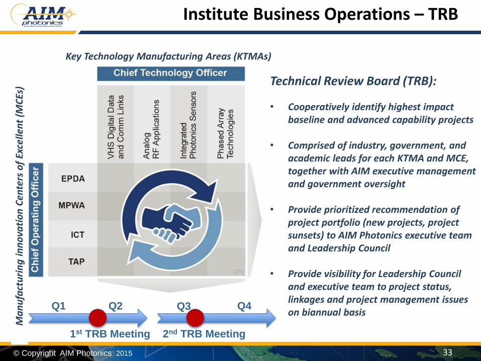
Institute Business Operations – TRB
33
Technical Review Board (TRB):
• Cooperatively identify highest impact baseline and advanced capability projects
• Comprised of industry, government, and academic leads for each KTMA and MCE, together with AIM executive management and government oversight
• Provide prioritized recommendation of project portfolio (new projects, project sunsets) to AIM Photonics executive team and Leadership Council
• Provide visibility for Leadership Council and executive team to project status, linkages and project management issues on biannual basis
Q1 Q2 Q3 Q4
1st TRB Meeting 2nd TRB Meeting
© Copyright AIM Photonics 2015
Key Technology Manufacturing Areas (KTMAs)
Ma
nu
fact
uri
ng
in
no
vati
on
Cen
ters
of
Exce
llen
t (M
CEs
)
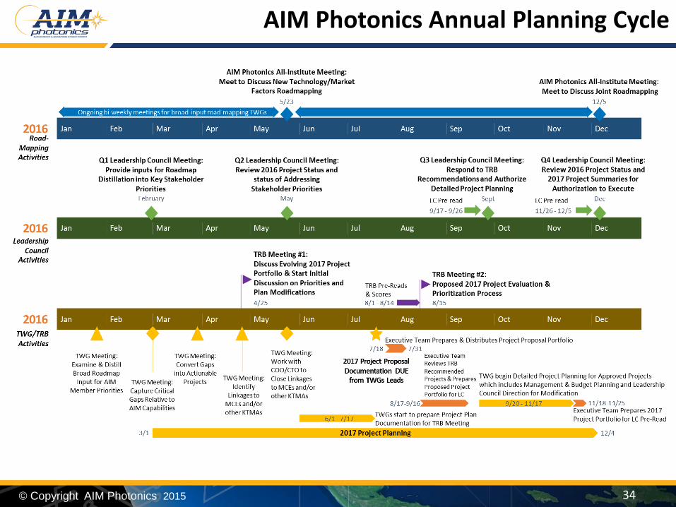
AIM Photonics Annual Planning Cycle
34© Copyright AIM Photonics 2015
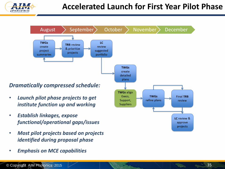
Accelerated Launch for First Year Pilot Phase
35
Dramatically compressed schedule:
• Launch pilot phase projects to get institute function up and working
• Establish linkages, expose functional/operational gaps/issues
• Most pilot projects based on projects identified during proposal phase
• Emphasis on MCE capabilities
© Copyright AIM Photonics 2015

Institute MCE’s Manufacturing Center of Excellences
36
EPDA Electronic Photonic Design Automation
Lead Peter Goetz NRLContacts Rob Scarmozzino Synopsys
Mike Watts MIT
Development of a set of integrated design tools for photonic and combined electronic-photonic components. Features: Models for Si and InP devices; Integrated electronic-photonic design environment; Design tools/PDK; and Intellectual Property protection.
MPWA Multi Project Wafer / Assembly
Lead Atilla Szep AFRLContacts Darwin Enicks Corning
Jeremiah Hebding SUNY Poly
Provision of full MPWA services including Foundry Broker and Foundry Operations for both Si and InP based photonic devices & components. Features: Availability of in-house 300mm Si and InP fabrication facilities; III-V laser integration; Interposer 2.5D/3D integration.
ICT Inline Control & Test
Lead Nick Usechak AFRLContacts Wilfried Haensch IBM
Douglas La Tulipe SUNY Poly
Robust optical testing for photonics applications using inline and stand-alone approaches. Features: High-throughput, high-functionality wafer-scale optical probe test; On wafer photonic test cells for process control; and Multi-channel I/O fiber array test interfaces.
TAP Test , Assembly & Optical Packaging
Lead Justin Bickford ARL Contacts Alan Evans Corning
Tom Brown UR
Development of standardized advanced automated, no-touch and accessible processes for PIC test, assembly & optical packaging. Features: Integration of 2D, 2.5D and 3D subassemblies into system-level package, fiber/WG attach, and pick and place capabilities; Sub-micron 3D inspection tools; and In-house prototype photonics optical packaging center.
© Copyright AIM Photonics 2015
Institute KTMA’s Key Technology Manufacturing Areas
37
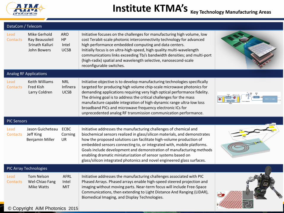
DataCom / Telecom
Lead Mike Gerhold ARO Contacts Ray Beausoleil HP
Srinath Kalluri IntelJohn Bowers UCSB
Initiative focuses on the challenges for manufacturing high volume, low cost Terabit-scale photonic interconnectivity technology for advanced high performance embedded computing and data centers. Initially focus is on ultra-high-speed, high quality multi-wavelength communications links exceeding Tb/s bandwidth densities; and multi-port (high-radix) spatial and wavelength selective, nanosecond-scale reconfigurable switches.
Analog RF Applications
Lead Keith Williams NRLContacts Fred Kish Infinera
Larry Coldren UCSB
Initiative objective is to develop manufacturing technologies specifically targeted for producing high volume chip-scale microwave photonics for demanding applications requiring very high optical performance fidelity. The driving goal is to address the critical challenges for the mass manufacture capable integration of high-dynamic range ultra-low loss broadband PICs and microwave frequency electronic ICs for unprecedented analog RF transmission communication performance.
PIC Sensors
Lead Jason Guicheteau ECBC Contacts Jeff King Corning
Benjamin Miller UR
Initiative addresses the manufacturing challenges of chemical and biochemical sensors realized in glass/silicon materials, and demonstrates how the proposed solutions can facilitate high-volume production of embedded sensors connecting to, or integrated with, mobile platforms. Goals include development and demonstration of manufacturing methods enabling dramatic miniaturization of sensor systems based on glass/silicon integrated photonics and novel engineered glass surfaces.
PIC Array Technologies
Lead Tom Nelson AFRL Contacts Wel-Chiao Fang Intel
Mike Watts MIT
Initiative addresses the manufacturing challenges associated with PIC Phased Arrays. Phased arrays enable high-speed steered projection and imaging without moving parts. Near-term focus will include Free-Space Communications, then extending to Light Distance And Ranging (LIDAR), Biomedical Imaging, and Display Technologies.
© Copyright AIM Photonics 2015
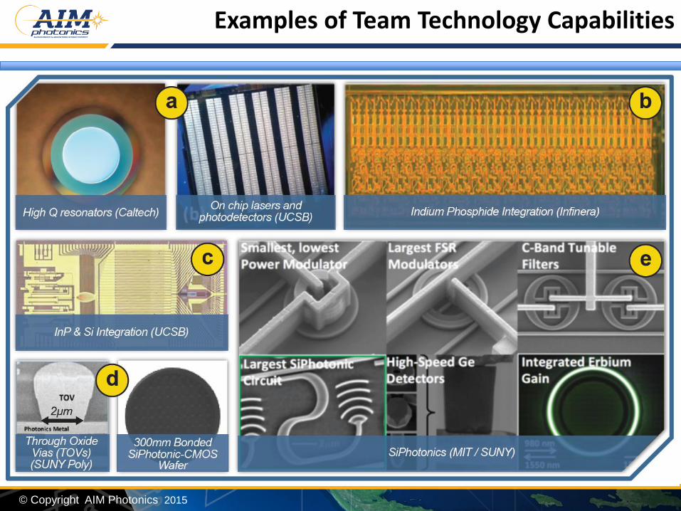
Examples of Team Technology Capabilities
© Copyright AIM Photonics 2015
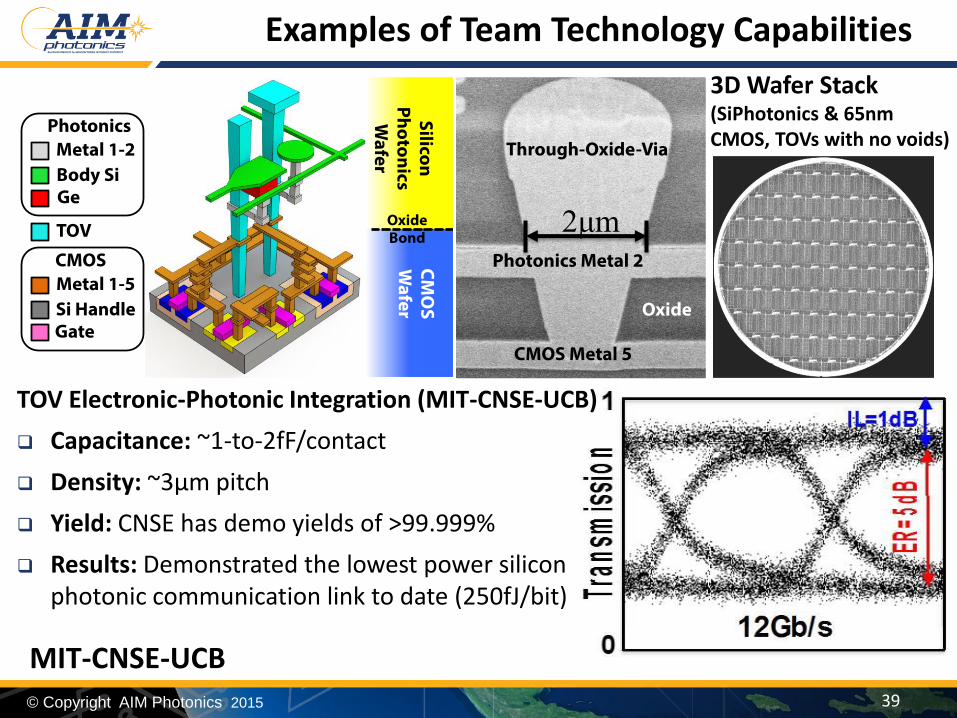
TOV Electronic-Photonic Integration (MIT-CNSE-UCB)
Capacitance: ~1-to-2fF/contact
Density: ~3μm pitch
Yield: CNSE has demo yields of >99.999%
Results: Demonstrated the lowest power silicon photonic communication link to date (250fJ/bit)
3D Wafer Stack(SiPhotonics & 65nm CMOS, TOVs with no voids)
2μm
MIT-CNSE-UCB39
Examples of Team Technology Capabilities
© Copyright AIM Photonics 2015
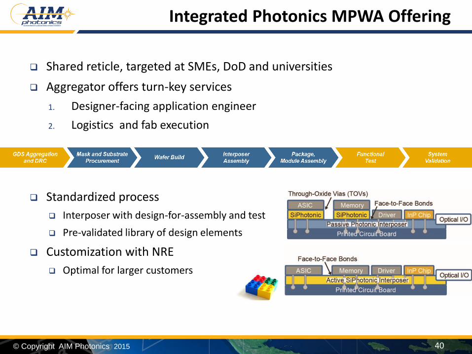
Integrated Photonics MPWA Offering
Shared reticle, targeted at SMEs, DoD and universities
Aggregator offers turn-key services
1. Designer-facing application engineer
2. Logistics and fab execution
Standardized process
Interposer with design-for-assembly and test
Pre-validated library of design elements
Customization with NRE
Optimal for larger customers
40© Copyright AIM Photonics 2015
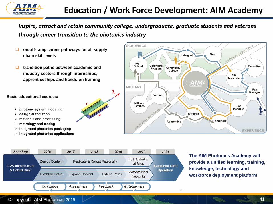
Education / Work Force Development: AIM Academy
41
Inspire, attract and retain community college, undergraduate, graduate students and veterans
through career transition to the photonics industry
p
n
l
photonic system modeling
design automation
materials and processing
metrology and testing
integrated photonics packaging
integrated photonics applications
Basic educational courses:
The AIM Photonics Academy will
provide a unified learning, training,
knowledge, technology and
workforce deployment platform
on/off-ramp career pathways for all supply
chain skill levels
transition paths between academic and
industry sectors through internships,
apprenticeships and hands-on training
© Copyright AIM Photonics 2015
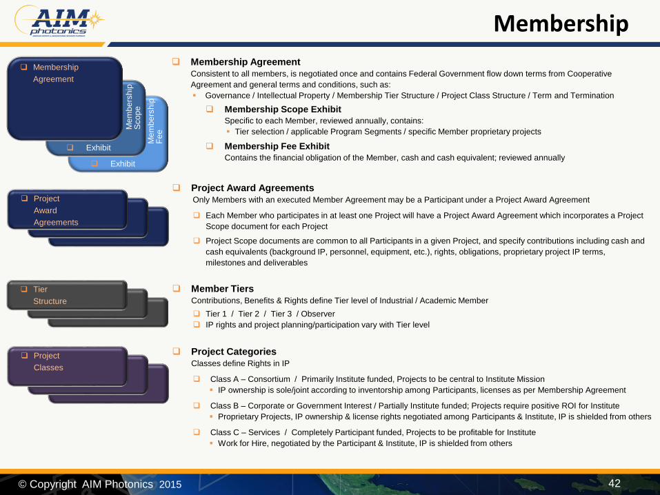
Membership
Agreement
Exhibit
Exhibit
Project
Award
Agreements
Membership Agreement Consistent to all members, is negotiated once and contains Federal Government flow down terms from Cooperative
Agreement and general terms and conditions, such as:
Governance / Intellectual Property / Membership Tier Structure / Project Class Structure / Term and Termination
Me
mb
ers
hip
S
co
pe
Me
mb
ers
hip
F
ee
Membership Scope Exhibit
Specific to each Member, reviewed annually, contains:
Tier selection / applicable Program Segments / specific Member proprietary projects
Membership Fee Exhibit
Contains the financial obligation of the Member, cash and cash equivalent; reviewed annually
Project Award Agreements Only Members with an executed Member Agreement may be a Participant under a Project Award Agreement
Each Member who participates in at least one Project will have a Project Award Agreement which incorporates a Project
Scope document for each Project
Project Scope documents are common to all Participants in a given Project, and specify contributions including cash and
cash equivalents (background IP, personnel, equipment, etc.), rights, obligations, proprietary project IP terms,
milestones and deliverables
42
Membership
Tier
Structure
Member TiersContributions, Benefits & Rights define Tier level of Industrial / Academic Member
Tier 1 / Tier 2 / Tier 3 / Observer
IP rights and project planning/participation vary with Tier level
Project
Classes
Project CategoriesClasses define Rights in IP
Class A – Consortium / Primarily Institute funded, Projects to be central to Institute Mission
IP ownership is sole/joint according to inventorship among Participants, licenses as per Membership Agreement
Class B – Corporate or Government Interest / Partially Institute funded; Projects require positive ROI for Institute
Proprietary Projects, IP ownership & license rights negotiated among Participants & Institute, IP is shielded from others
Class C – Services / Completely Participant funded, Projects to be profitable for Institute
Work for Hire, negotiated by the Participant & Institute, IP is shielded from others
© Copyright AIM Photonics 2015
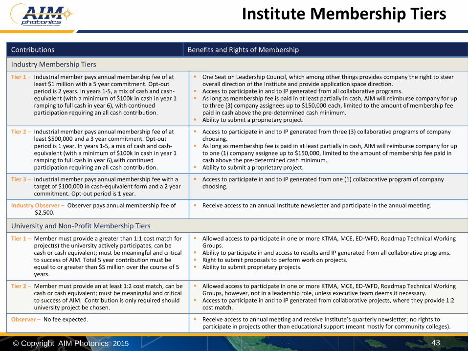
Contributions Benefits and Rights of Membership
Industry Membership Tiers
Tier 1 – Industrial member pays annual membership fee of at least $1 million with a 5 year commitment. Opt-out period is 2 years. In years 1-5, a mix of cash and cash-equivalent (with a minimum of $100k in cash in year 1 ramping to full cash in year 6), with continued participation requiring an all cash contribution.
One Seat on Leadership Council, which among other things provides company the right to steer overall direction of the Institute and provide application space direction.
Access to participate in and to IP generated from all collaborative programs. As long as membership fee is paid in at least partially in cash, AIM will reimburse company for up
to three (3) company assignees up to $150,000 each, limited to the amount of membership fee paid in cash above the pre-determined cash minimum.
Ability to submit a proprietary project.
Tier 2 – Industrial member pays annual membership fee of at least $500,000 and a 3 year commitment. Opt-out period is 1 year. In years 1-5, a mix of cash and cash-equivalent (with a minimum of $100k in cash in year 1 ramping to full cash in year 6),with continued participation requiring an all cash contribution.
Access to participate in and to IP generated from three (3) collaborative programs of company choosing.
As long as membership fee is paid in at least partially in cash, AIM will reimburse company for up to one (1) company assignee up to $150,000, limited to the amount of membership fee paid in cash above the pre-determined cash minimum.
Ability to submit a proprietary project.
Tier 3 – Industrial member pays annual membership fee with a target of $100,000 in cash-equivalent form and a 2 year commitment. Opt-out period is 1 year.
Access to participate in and to IP generated from one (1) collaborative program of company choosing.
Industry Observer – Observer pays annual membership fee of $2,500.
Receive access to an annual Institute newsletter and participate in the annual meeting.
University and Non-Profit Membership Tiers
Tier 1 – Member must provide a greater than 1:1 cost match for project(s) the university actively participates, can be cash or cash equivalent; must be meaningful and critical to success of AIM. Total 5 year contribution must be equal to or greater than $5 million over the course of 5 years.
Allowed access to participate in one or more KTMA, MCE, ED-WFD, Roadmap Technical Working Groups.
Ability to participate in and access to results and IP generated from all collaborative programs. Right to submit proposals to perform work on projects. Ability to submit proprietary projects.
Tier 2 – Member must provide an at least 1:2 cost match, can be cash or cash equivalent; must be meaningful and critical to success of AIM. Contribution is only required should university project be chosen.
Allowed access to participate in one or more KTMA, MCE, ED-WFD, Roadmap Technical Working Groups, however, not in a leadership role, unless executive team deems it necessary.
Access to participate in and to IP generated from collaborative projects, where they provide 1:2 cost match.
Observer – No fee expected. Receive access to annual meeting and receive Institute’s quarterly newsletter; no rights to participate in projects other than educational support (meant mostly for community colleges).
43© Copyright AIM Photonics 2015
Institute Membership Tiers
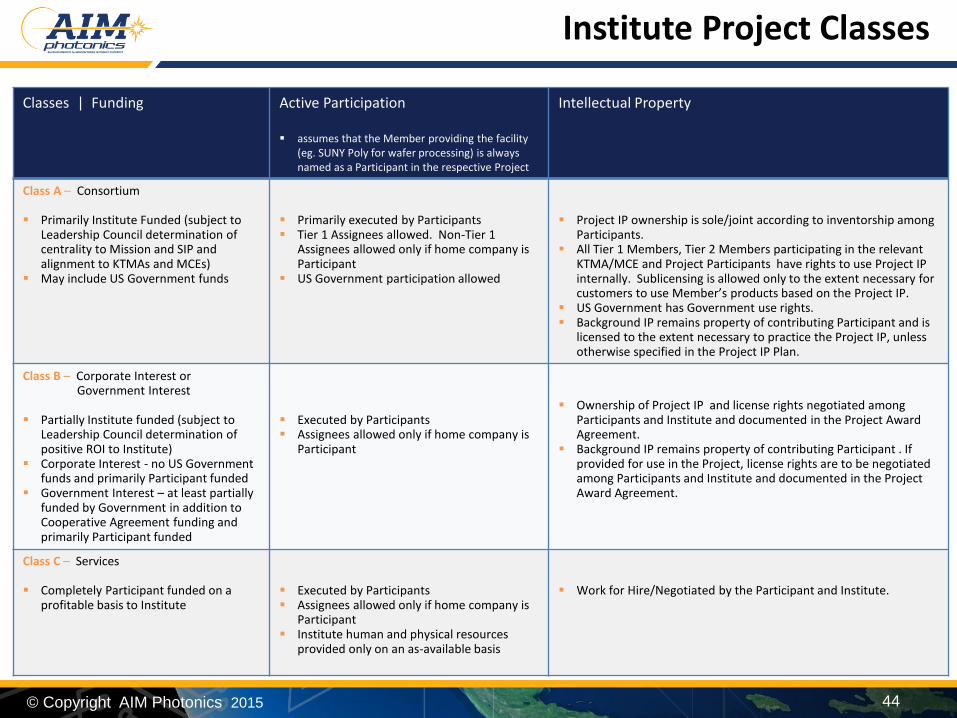
Classes | Funding Active Participation
assumes that the Member providing the facility (eg. SUNY Poly for wafer processing) is always named as a Participant in the respective Project
Intellectual Property
Class A – Consortium
Primarily Institute Funded (subject to Leadership Council determination of centrality to Mission and SIP and alignment to KTMAs and MCEs)
May include US Government funds
Primarily executed by Participants Tier 1 Assignees allowed. Non-Tier 1
Assignees allowed only if home company is Participant
US Government participation allowed
Project IP ownership is sole/joint according to inventorship among Participants.
All Tier 1 Members, Tier 2 Members participating in the relevant KTMA/MCE and Project Participants have rights to use Project IP internally. Sublicensing is allowed only to the extent necessary for customers to use Member’s products based on the Project IP.
US Government has Government use rights. Background IP remains property of contributing Participant and is
licensed to the extent necessary to practice the Project IP, unless otherwise specified in the Project IP Plan.
Class B – Corporate Interest or Government Interest
Partially Institute funded (subject to Leadership Council determination of positive ROI to Institute)
Corporate Interest - no US Government funds and primarily Participant funded
Government Interest – at least partially funded by Government in addition to Cooperative Agreement funding and primarily Participant funded
Executed by Participants Assignees allowed only if home company is
Participant
Ownership of Project IP and license rights negotiated among Participants and Institute and documented in the Project Award Agreement.
Background IP remains property of contributing Participant . If provided for use in the Project, license rights are to be negotiated among Participants and Institute and documented in the Project Award Agreement.
Class C – Services
Completely Participant funded on a profitable basis to Institute
Executed by Participants Assignees allowed only if home company is
Participant Institute human and physical resources
provided only on an as-available basis
Work for Hire/Negotiated by the Participant and Institute.
44
Institute Project Classes
© Copyright AIM Photonics 2015
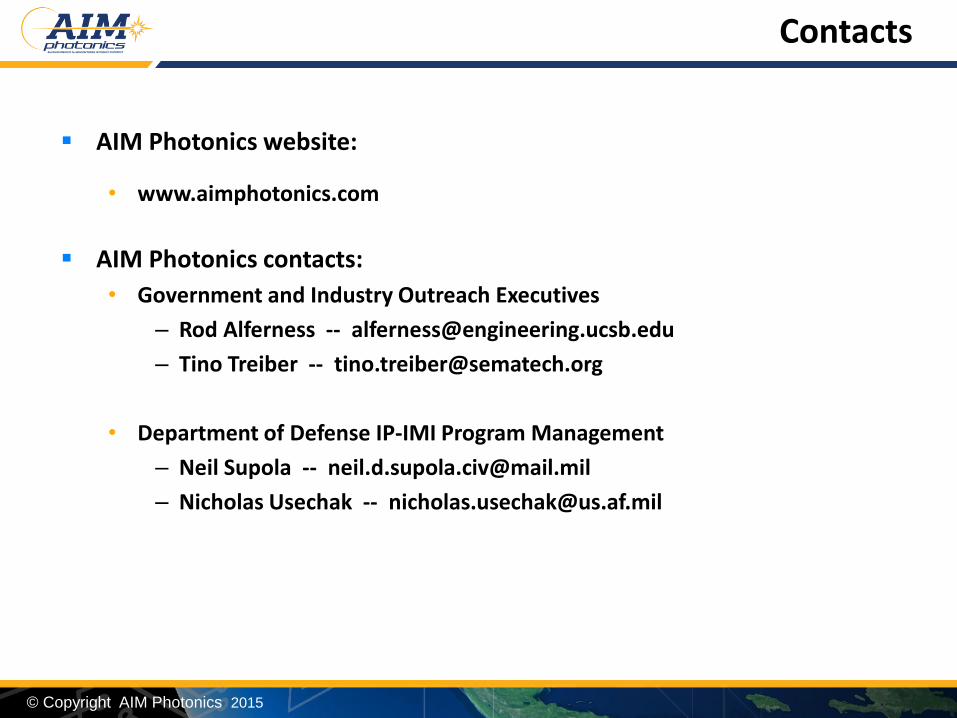
AIM Photonics website:
• www.aimphotonics.com
AIM Photonics contacts:
• Government and Industry Outreach Executives
– Rod Alferness -- [email protected]
– Tino Treiber -- [email protected]
• Department of Defense IP-IMI Program Management
– Neil Supola -- [email protected]
– Nicholas Usechak -- [email protected]
Contacts
© Copyright AIM Photonics 2015
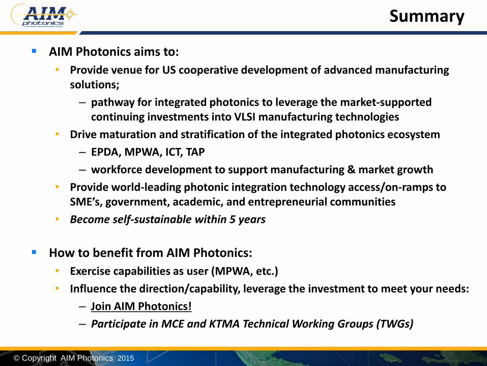
AIM Photonics aims to:
• Provide venue for US cooperative development of advanced manufacturing solutions;
– pathway for integrated photonics to leverage the market-supported continuing investments into VLSI manufacturing technologies
• Drive maturation and stratification of the integrated photonics ecosystem
– EPDA, MPWA, ICT, TAP
– workforce development to support manufacturing & market growth
• Provide world-leading photonic integration technology access/on-ramps to SME’s, government, academic, and entrepreneurial communities
• Become self-sustainable within 5 years
How to benefit from AIM Photonics:
• Exercise capabilities as user (MPWA, etc.)
• Influence the direction/capability, leverage the investment to meet your needs:
– Join AIM Photonics!
– Participate in MCE and KTMA Technical Working Groups (TWGs)
Summary
© Copyright AIM Photonics 2015
Q&A
Dr. Tom Baer
Past chair
NPI Steering Committee
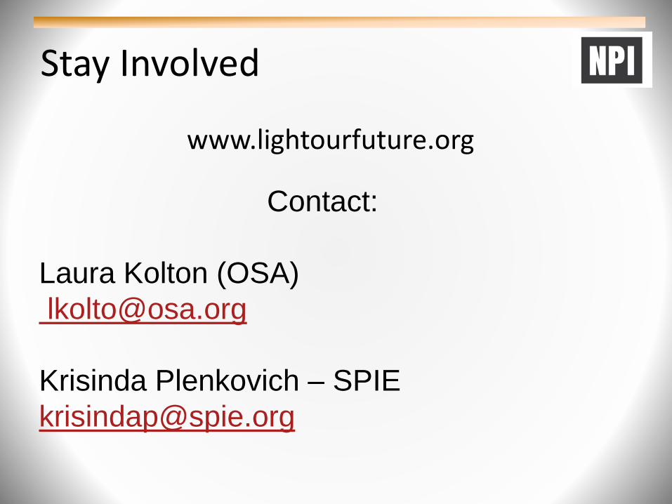
Stay Involved
www.lightourfuture.org
Contact:
Laura Kolton (OSA)
Krisinda Plenkovich – SPIE