
AN 523: Cyclone III Family Devices Configuration Interface ... · Cyclone III family devices, you...
20
© July 2012 Altera Corporation AN 523: Cyclone III Devices Configuration Interface Guidelines with EPCS Devices AN-523-1.2 © July 2012 AN 523: Cyclone III Devices Configuration Interface Guidelines with EPCS Devices Introduction This application note provides the guidelines to Cyclone ® III family devices (Cyclone III and Cyclone III LS devices) interfacing with a serial configuration device (EPCS) using 3.0-V and 2.5-V I/O voltages, in addition to the standard 3.3 V. This application note also discusses the electrical specifications, timing requirements, signal integrity analysis, and board physical design guidelines for the supported active serial (AS) configuration schemes. Bank 1 of Cyclone III family devices is used for AS configuration signals and for user I/Os. The I/O voltage for Cyclone III family devices AS configuration signals must be compatible with the operating voltage of Altera ® EPCS devices and must not conflict with the intended I/O voltages for other bank 1 signals. The Altera EPCS devices support supply voltage from 2.7 V to 3.6 V, which enables the EPCS devices to operate at 3.3 V or 3.0 V. This application note shows the methods to use 3.0- and 2.5-V bank 1 I/O voltages of Cyclone III family devices with the EPCS device. Additionally, at any I/O voltages of 3.3, 3.0, or 2.5 V of Cyclone III family devices, this application note shows how to create a robust electrical and physical board design to interface with an EPCS device using single and multi-device AS configuration. You can create your design based on the signal integrity analysis and physical design constraints in this application note to achieve a successful AS configuration. AS Interfacing Overview This section provides an overview on the method to interface a Cyclone III device family to an EPCS device using 3.3-, 3.0-, or 2.5-V bank 1 I/O voltages of Cyclone III family devices. Detailed discussion on the electrical specification compatibility and requirements are discussed in “Electrical Specification Compatibility” on page 2. Step 1: Choose the Appropriate Voltage Levels for Cyclone III Family Devices I/O Bank 1 and EPCS Supply The EPCS device operates at 3.3 V or 3.0 V. When the AS configuration scheme is selected, I/O bank 1 of Cyclone III family devices allows I/O voltages of 3.3, 3.0, or 2.5 V. You can operate Cyclone III family devices I/O bank 1 and the EPCS device at any combinations of the allowable operating voltages. For example, if I/O bank 1 of Cyclone III family devices is required to be at 2.5 V for the LVDS I/O signals and 3.3-V supplies are readily available, supply the EPCS device with 3.3 V. Another example is if a 3.0-V I/O voltage is used in bank 1 of Cyclone III family devices, you must supply the EPCS device with the same 3.0 V to avoid designing a 3.3-V regulator dedicated for the EPCS device. f The electrical specification compatibility between different voltage levels is further discussed in “Electrical Specification Compatibility” on page 2.
Transcript of AN 523: Cyclone III Family Devices Configuration Interface ... · Cyclone III family devices, you...

© July 2012 Altera Corporation
© July 2012
AN 523: Cyclone III Devices Configuration Interface Guidelines with
EPCS Devices
AN-523-1.2IntroductionThis application note provides the guidelines to Cyclone® III family devices (Cyclone III and Cyclone III LS devices) interfacing with a serial configuration device (EPCS) using 3.0-V and 2.5-V I/O voltages, in addition to the standard 3.3 V. This application note also discusses the electrical specifications, timing requirements, signal integrity analysis, and board physical design guidelines for the supported active serial (AS) configuration schemes.
Bank 1 of Cyclone III family devices is used for AS configuration signals and for user I/Os. The I/O voltage for Cyclone III family devices AS configuration signals must be compatible with the operating voltage of Altera® EPCS devices and must not conflict with the intended I/O voltages for other bank 1 signals. The Altera EPCS devices support supply voltage from 2.7 V to 3.6 V, which enables the EPCS devices to operate at 3.3 V or 3.0 V. This application note shows the methods to use 3.0- and 2.5-V bank 1 I/O voltages of Cyclone III family devices with the EPCS device.
Additionally, at any I/O voltages of 3.3, 3.0, or 2.5 V of Cyclone III family devices, this application note shows how to create a robust electrical and physical board design to interface with an EPCS device using single and multi-device AS configuration. You can create your design based on the signal integrity analysis and physical design constraints in this application note to achieve a successful AS configuration.
AS Interfacing OverviewThis section provides an overview on the method to interface a Cyclone III device family to an EPCS device using 3.3-, 3.0-, or 2.5-V bank 1 I/O voltages of Cyclone III family devices. Detailed discussion on the electrical specification compatibility and requirements are discussed in “Electrical Specification Compatibility” on page 2.
Step 1: Choose the Appropriate Voltage Levels for Cyclone III Family Devices I/O Bank 1 and EPCS Supply
The EPCS device operates at 3.3 V or 3.0 V. When the AS configuration scheme is selected, I/O bank 1 of Cyclone III family devices allows I/O voltages of 3.3, 3.0, or 2.5 V. You can operate Cyclone III family devices I/O bank 1 and the EPCS device at any combinations of the allowable operating voltages.
For example, if I/O bank 1 of Cyclone III family devices is required to be at 2.5 V for the LVDS I/O signals and 3.3-V supplies are readily available, supply the EPCS device with 3.3 V. Another example is if a 3.0-V I/O voltage is used in bank 1 of Cyclone III family devices, you must supply the EPCS device with the same 3.0 V to avoid designing a 3.3-V regulator dedicated for the EPCS device.
f The electrical specification compatibility between different voltage levels is further discussed in “Electrical Specification Compatibility” on page 2.
AN 523: Cyclone III Devices Configuration Interface Guidelines with EPCS Devices
Page 2 Electrical Specification Compatibility
Step 2: Select the Corresponding MSEL Settings Based on Configuration Voltage LevelsWhen the I/O voltage for Cyclone III family devices AS configuration signals is determined, select the right AS configuration MSEL settings based on the selected I/O voltage level. For example, if you use 2.5 V to power bank 1 of Cyclone III family devices, select the MSEL setting for 3.0 or 2.5 V configuration voltage level. The MSEL setting is independent of the EPCS supply level.
f For more information on the valid AS MSEL settings, refer to the Configuration, Design Security, and Remote System Upgrades in Cyclone III Devices chapter in volume 1 of the Cyclone III Device Handbook.
Step 3: Design Board Interface According to Recommended ConnectionsAltera provides the recommended interface setup between Cyclone III family devices and the EPCS device for the supported AS configuration schemes. The passive components in the interfaces are recommended for optimal signal integrity during configuration and EPCS programming.
f For the interface connections, refer to the Active Serial Configuration (Serial Configuration Devices) section in the Configuration, Design Security, and Remote System Upgrades in Cyclone III Devices chapter in volume 1 of the Cyclone III Device Handbook.
A detailed board design constraints and signal integrity analysis is discussed in “Board Design Constraints and Analysis” on page 5.
Electrical Specification CompatibilityThis section describes the electrical specification compatibility between Cyclone III family devices and the EPCS device at various configuration voltage levels.
In an interface, a receiver must interpret the logic-level correctly from the driver. The DC specifications for an I/O determine the appropriate logic-level voltage for the driver and receiver. The DC parameters that define the logic voltage levels are:
■ VIH (Voltage Input High): The minimum positive voltage applied to the input which is accepted by the device as a logic-high.
■ VIL (Voltage Input Low): The maximum positive voltage applied to the input which is accepted by the device as a logic-low.
■ VOH (Voltage Output High): The minimum positive voltage from an output which the device considers is accepted as the minimum positive high-level.
■ VOL (Voltage Output Low): The maximum positive voltage from an output which the device considers is accepted as the maximum positive low-level.
AN 523: Cyclone III Devices Configuration Interface Guidelines with EPCS Devices © July 2012 Altera Corporation
Electrical Specification Compatibility Page 3
An interface is operable when the difference between what the driver outputs as a valid logic voltage and what the receiver expects to receive as a valid logic voltage is zero or positive in value. The difference is commonly known as noise margin. In reference to the DC parameters, an operable interface must meet these conditions:
1. VOH VIH
2. VOL VIL
Therefore the noise margins are expressed as:
1. High-level noise margin = VOH – VIH
2. Low-level noise margin = VIL – VOL
Positive noise margin indicates better required noise immunity, while negative value indicates inoperability. In a system, extra noise margin is the voltage budget to accommodate for board-level noise such as power supply variation, trace coupling noise, signal reflection, and switching noise.
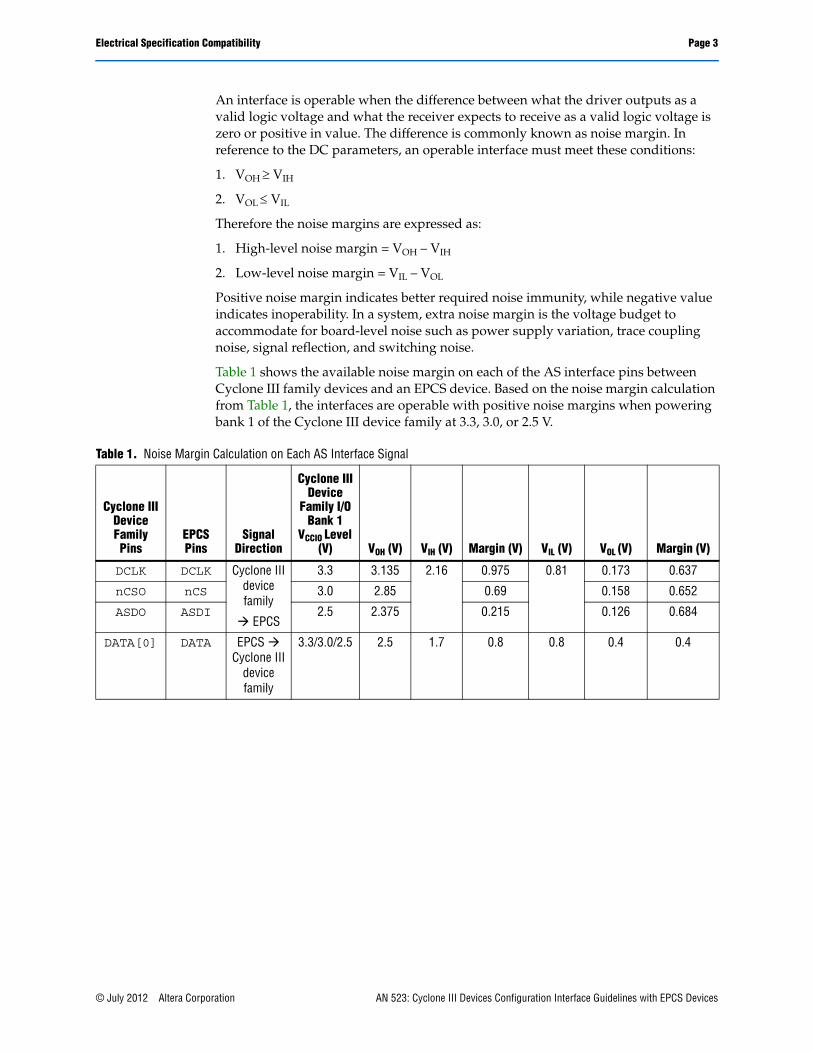
Table 1 shows the available noise margin on each of the AS interface pins between Cyclone III family devices and an EPCS device. Based on the noise margin calculation from Table 1, the interfaces are operable with positive noise margins when powering bank 1 of the Cyclone III device family at 3.3, 3.0, or 2.5 V.
Table 1. Noise Margin Calculation on Each AS Interface Signal
Cyclone III Device Family Pins
EPCS Pins
Signal Direction
Cyclone III Device
Family I/O Bank 1
VCCIO Level (V) VOH (V) VIH (V) Margin (V) VIL (V) VOL (V) Margin (V)
DCLK DCLK Cyclone III device family
EPCS
3.3 3.135 2.16 0.975 0.81 0.173 0.637
nCSO nCS 3.0 2.85 0.69 0.158 0.652
ASDO ASDI 2.5 2.375 0.215 0.126 0.684
DATA[0] DATA EPCS Cyclone III
device family
3.3/3.0/2.5 2.5 1.7 0.8 0.8 0.4 0.4
© July 2012 Altera Corporation AN 523: Cyclone III Devices Configuration Interface Guidelines with EPCS Devices

Page 4 Electrical Specification Compatibility
Figure 1 and Figure 2 illustrate the noise margin for each signal direction.
Table 1 assumes the worst value of DC parameters for interfacing, whereas Table 2 describes the worst DC operating conditions for an EPCS device.
Figure 1. High and Low-Level Noise Margin for DCLK, nCSO and ASDO Pins
Figure 2. High and Low-Level Noise Margin for DATA[O] Pin
Table 2. Worst DC Operating Conditions of the EPCS Device
Parameter Specification Worst case Unit
Vcc 2.7–3.6 — V
VIH 0.6×Vcc 2.16 V
VIL 0.3×Vcc 0.81 V
VOH (Ioh= -0.1 mA) Vcc-0.2 2.5 V
VOL (Iol=1.6 mA) 0.4 0.4 V
0
Invalid Level
Low-level noise margin
Worst high-level noise margin
CCIO
0.81 (V )IL
2.16 (V )IH
VCC
0.173 V
V = 3.135 V
CCIOV = 2.375 VCCIO
V = 2.85 VCCIO
Driver’s Output Level Receiver’s Threshold
0
Invalid Level
Low-level noise margin
High-level noise margin
0.8 (V )IL
1.7 (V )IH
VCC
OH2.5 (V )
IL0.4 (V )
(V)
Driver’s Output Level Receiver’s Threshold
AN 523: Cyclone III Devices Configuration Interface Guidelines with EPCS Devices © July 2012 Altera Corporation
Board Design Constraints and Analysis Page 5
Cyclone III family devices AS configuration output pins are designed to interface with EPCS devices. The high- and low-level outputs for Cyclone III family devices AS configuration pins are assumed at VCCIO and ground level respectively in the interface with the EPCS device. Such an assumption is possible as the interface does not draw DC current at steady voltage levels. Being a CMOS device, the EPCS input leakage current is at a mere ±10 A. In addition, there is no external component that draws DC current in all recommended setup connections.
The DC parameters for the Cyclone III device family AS input pin are described in Table 3.
In any unterminated interface, impedance mismatch between the driver, board trace, and load results in noise reflections such as overshoot, undershoot, and ringing. The magnitude of voltage deviations is harmful to the receiving device. When designing interfaces with Cyclone III family devices, maximum allowable transient input voltage must be met according to the Cyclone III Device Data Sheet and Cyclone III LS Device Data Sheet chapters in volume 2 of the Cyclone III Device Handbook.
The EPCS device has high current capability which makes it suitable for high loading conditions such as multi-device configuration setup with multiple FPGAs. The high current capability contributes to larger reflection noise in a single point-to-point interface such a single-device AS configuration with Cyclone III family devices. In such case, ensure that the magnitude of overshoot noise seen at Cyclone III family devices input pins stay within the allowable limits. Employ external mitigation techniques such as series termination to control the impedance mismatch and the resulting reflection noise.
Board Design Constraints and AnalysisThis section describes the board design constraints when using the AS configuration scheme with Cyclone III family devices. The signal integrity analysis covered in this section provides an insight into the interface signal quality concerns and how the concerns are mitigated with the recommended passive components in various supported AS configuration setups.
Table 3. DC Operating Conditions of the Cyclone III Device Family AS Configuration Pins
Parameter Specification Worst case Unit
VIH 1.7 1.7 V
VIL 0.7 0.7 V
© July 2012 Altera Corporation AN 523: Cyclone III Devices Configuration Interface Guidelines with EPCS Devices
Page 6 Board Design Constraints and Analysis
General Board Design ConstraintsAt any of Cyclone III family devices and the EPCS device operating voltages, there are two general board design constraints. They are:
1. For board with FR4 dielectric material, the total trace length between each AS pin from Cyclone III family devices to the EPCS device must not exceed 10 inches.
■ For other board materials, determine the equivalent trace length that contributes the same signal propagation delay relative to the FR4.
2. Maximum capacitance load seen on the DCLK pin of Cyclone III family devices must not exceed 15 pF.
■ As comparison, maximum pin capacitance on any EPCS device is 6 pF.
■ This constraint is mainly applicable in multi-device setup which limits the pin capacitance of a repeater buffer to approximately 9 pF.
The constraints that ensure the delay between Cyclone III family devices pin and the EPCS pin is within an acceptable range to meet the timing requirements of the system for read (configuration phase) and write (programming phase) operations. Inter-operability between a Cyclone III device family and an EPCS device cannot be guaranteed if the above constraints are exceeded in any design.
1 Altera does not recommend the usage of external level translator between Cyclone III family devices and an EPCS device for an AS configuration due to the timing requirements.
Signal Integrity ConcernsThe DCLK signal must be monotonous during logic transitions between the VIH and VIL voltage region at the EPCS device. A non-monotonic transition on DCLK input is interpreted as a second clocking event and results in unintended double-clocking. The EPCS DATA signal also requires impedance matching to board trace for optimal signal integrity. Driving the DATA signal directly to the DATA[0] input pin of the Cyclone III device family results in an overshoot that exceeds the maximum allowable transient input voltage.
1 A monotonic transition is when the signal is consistently changing only in one direction. For example, in a rising transition, a monotonic signal consistently rises from logic-low level to logic-high level without reversing in direction. On the contrary, in a falling transition, a monotonic signal consistently falls from logic-high level to logic-low level without reversing in direction.
EPCS devices operate in a synchronous mode based on the DCLK input signal. ASDI and DATA signals function within a set of timing parameters relative to the DCLK transition edges. In the event of double-clocking, incorrect data is latched and results in configuration failure. Board routing and path topological setup affects the integrity of a signal. Therefore, emphasis on signal integrity is required for the DCLK signal. With the constraints on board trace length and load limit, data pins such as ASDI and DATA have sufficient timing margin prior to data sampling to account for signal integrity-induced delays.
AN 523: Cyclone III Devices Configuration Interface Guidelines with EPCS Devices © July 2012 Altera Corporation

Board Design Constraints and Analysis Page 7
Analysis and RecommendationsThis section describes the signal integrity analysis and recommendations for each supported AS configuration scheme with Cyclone III family devices.
The following are the simulation setup information used throughout this section:
■ All simulations are performed using IBIS models in slow (worst) conditions (weakest process corner, low voltage, and high temperature) unless stated otherwise.
■ All simulations are performed using Hyperlynx® LineSim® version 7.7 by Mentor Graphics® Corporation.
■ IBIS file revisions used for simulations:
■ Altera Cyclone III version 2.1 (February 2008)
■ Altera EPCS 1-4 version 1.2 (February 2005)
■ Altera EPCS 16 version 1.0 (February 2005)
■ Phillips 74LVC244A version 1.2 (November 2002)
f IBIS models for all Altera devices are available at the Altera IBIS Models page on the Altera website.
Single-Device AS Configuration This is the simplest setup of an EPCS device with a Cyclone III device family.
Figure 3 illustrates the recommended setup.
Each Cyclone III family devices AS output drivers (DCLK, nCSO, and ASDO) are designed with the capability to directly drive to the targeted EPCS inputs.
Figure 3. Single-Device AS Configuration Recommended Setup
Serial Configuration Device
DATADCLKnCSASDI
25 ΩDATA[0]DCLKnCSOASDO
Cyclone III DeviceFamily
© July 2012 Altera Corporation AN 523: Cyclone III Devices Configuration Interface Guidelines with EPCS Devices
Page 8 Board Design Constraints and Analysis
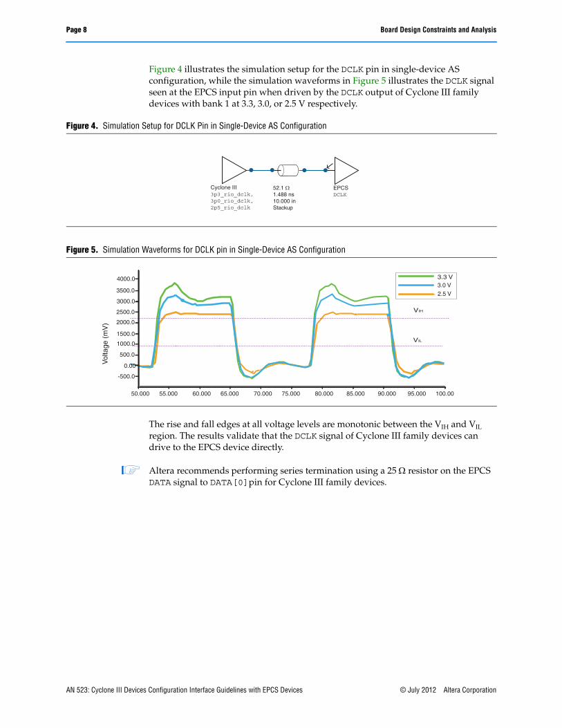
Figure 4 illustrates the simulation setup for the DCLK pin in single-device AS configuration, while the simulation waveforms in Figure 5 illustrates the DCLK signal seen at the EPCS input pin when driven by the DCLK output of Cyclone III family devices with bank 1 at 3.3, 3.0, or 2.5 V respectively.
The rise and fall edges at all voltage levels are monotonic between the VIH and VIL region. The results validate that the DCLK signal of Cyclone III family devices can drive to the EPCS device directly.
1 Altera recommends performing series termination using a 25 resistor on the EPCS DATA signal to DATA[0]pin for Cyclone III family devices.
Figure 4. Simulation Setup for DCLK Pin in Single-Device AS Configuration
Figure 5. Simulation Waveforms for DCLK pin in Single-Device AS Configuration
Cyclone III3p3_rio_dclk, 3p0_rio_dclk, 2p5_rio_dclk
52.1 Ω 1.488 ns10.000 inStackup
EPCSDCLK
3.3 V
VIH
VIL
Vol
tage
(m
V)
-500.0
500.0
1500.0
2500.0
3500.0
50.000 55.000 60.000 65.000 70.000 75.000 80.000 85.000 90.000 95.000 100.00
3000.0
2000.0
1000.0
0.00
4000.03.0 V2.5 V
AN 523: Cyclone III Devices Configuration Interface Guidelines with EPCS Devices © July 2012 Altera Corporation
Board Design Constraints and Analysis Page 9
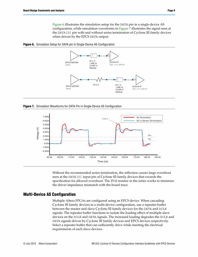
Figure 6 illustrates the simulation setup for the DATA pin in a single-device AS configuration, while simulation waveforms in Figure 7 illustrates the signal seen at the DATA[0] pin with and without series termination of Cyclone III family devices when driven by the EPCS DATA output.
Without the recommended series termination, the reflection causes large overshoot seen at the DATA[0] input pin of Cyclone III family devices that exceeds the specification for allowed overshoot. The 25 resistor in the series works to minimize the driver impedance mismatch with the board trace.
Multi-Device AS Configuration Multiple Altera FPGAs are configured using an EPCS device. When cascading Cyclone III family devices in a multi-device configuration, use a repeater buffer between the master and slave Cyclone III family devices for the DATA and DCLK signals. The repeater buffer functions to isolate the loading effect of multiple slave devices on the DCLK and DATA signals. The increased loading degrades the DCLK and DATA signals driven by Cyclone III family devices and EPCS devices respectively. Select a repeater buffer that can sufficiently drive while meeting the electrical requirements of each slave devices.
Figure 6. Simulation Setup for DATA pin in Single-Device AS Configuration
Figure 7. Simulation Waveforms for DATA Pin in Single-Device AS Configuration
52.1 Ω1.488 ns10.000 inStackup
EPCS16SI16NDATA
52.1 Ω1.488 ns10.000 inStackup
Cyclone III 3p3_rio_data0
EPCS16SI16NDATA
25.0 ΩCyclone III 3p3_rio_data0
5.26 V
Time (ns)
Vol
tage
(V
)
-2.000
0.00
2.000
4.000
6.000
90.00 100.00 110.00 120.00 130.00 140.00 150.00 160.00 170.00 180.00 190.00
5.000
3.000
1.000
7.000
-1.000
No Termination
25 Ω Series Termination
VIH
VIL
© July 2012 Altera Corporation AN 523: Cyclone III Devices Configuration Interface Guidelines with EPCS Devices
Page 10 Board Design Constraints and Analysis
f For the requirements to select a suitable repeater buffer, refer to the Configuration and JTAG Pin I/O Requirements section in the Configuration, Design Security, and Remote System Upgrades in Cyclone III Devices chapter of the Cyclone III Device Handbook.
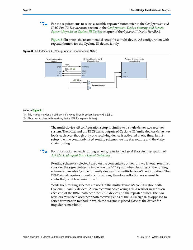
Figure 8 illustrates the recommended setup for a multi-device AS configuration with repeater buffers for the Cyclone III device family.
The multi-device AS configuration setup is similar to a single driver two receiver system. The DCLK and the EPCS DATA outputs of Cyclone III family devices drive two loads each even though only one receiving device is activated at one time. In this setup, the two commonly used routing schemes are the star routing and the daisy chain routing.
f For information on each routing scheme, refer to the Signal Trace Routing section of AN 224: High-Speed Board Layout Guidelines.
Routing scheme is selected based on the convenience of board trace layout. You must consider the signal integrity impact on the DCLK path when deciding on the routing scheme to cascade Cyclone III family devices in a multi-device AS configuration. The DCLK signal requires monotonic transitions, therefore reflection noise must be controlled, or at least minimized.
While both routing schemes are used in the multi-device AS configuration with Cyclone III family devices, Altera recommends placing a 50 resistor in series on each end of the DCLK path near the EPCS device and the repeater buffer. The two resistors must be placed near both receiving ends of the DCLK signal, as opposed to series termination method in which the resistor is placed close to the driver for impedance matching.
Figure 8. Multi-Device AS Configuration Recommended Setup
Notes to Figure 8:
(1) This resistor is optional if I/O bank 1 of Cyclone III family devices is powered at 3.3 V.(2) Place resistor close to the receiving device (EPCS or repeater buffers).
50 Ω
DATA
DCLKnCSASDI
DCLK
DATA[0]
DATA[0]
DCLKnCSOASDO
Serial Configuration Device
Cyclone III device family Master Device
Cyclone III device family Slave Device
25 Ω
50 Ω
repeater buffers
(1), (2)(1), (2)
(1), (2)(1), (2)
AN 523: Cyclone III Devices Configuration Interface Guidelines with EPCS Devices © July 2012 Altera Corporation

Board Design Constraints and Analysis Page 11
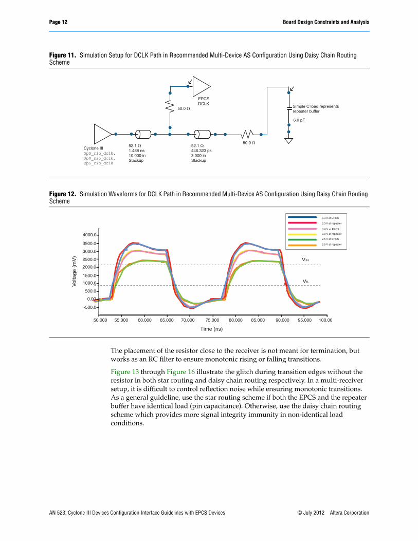
Figure 9 and Figure 11 illustrate the cases in which the DCLK output is powered by 3.3, 3.0, or 2.5 V respectively. You must keep the stub in daisy chain routing scheme at minimal length to improve signal integrity. Simulation waveforms in Figure 10 and Figure 12 illustrate the DCLK signal seen at the EPCS input pin and the repeater buffer with Altera's recommended setup for both star routing and daisy chain routing, respectively.
Figure 9. Simulation Setup for DCLK Path in Recommended Multi-Device AS Configuration Using Star Routing Scheme
Figure 10. Simulation Waveforms for DCLK Path in Recommended Multi-Device AS Configuration Using Star Routing Scheme
Cyclone III3p3_rio_dclk, 3p0_rio_dclk, 2p5_rio_dclk
52.1 Ω892.645 ps6.000 inStackup
52.1 Ω595.097 ps4.000 in Stackup
52.1 Ω595.097 ps4.000 in Stackup
50.0 Ω
50.0 Ω
EPCSDCLK
6.0 pF
Simple C load represents repeater buffer
Vol
tage
(m
V)
-500.0
500.0
1500.0
2500.0
3500.0
50.000 55.000 60.000 65.000 70.000 75.000 80.000 85.000 90.000 95.000 100.00
3000.0
2000.0
1000.0
4000.0
0.00
VIH
VIL
3.3 V at EPCS
3.3 V at repeater
3.0 V at EPCS
3.0 V at repeater
2.5 V at EPCS
2.5 V at repeater
© July 2012 Altera Corporation AN 523: Cyclone III Devices Configuration Interface Guidelines with EPCS Devices
Page 12 Board Design Constraints and Analysis
The placement of the resistor close to the receiver is not meant for termination, but works as an RC filter to ensure monotonic rising or falling transitions.
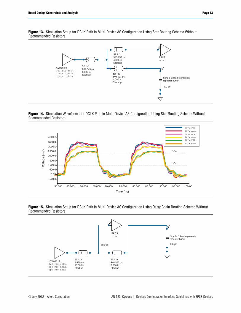
Figure 13 through Figure 16 illustrate the glitch during transition edges without the resistor in both star routing and daisy chain routing respectively. In a multi-receiver setup, it is difficult to control reflection noise while ensuring monotonic transitions. As a general guideline, use the star routing scheme if both the EPCS and the repeater buffer have identical load (pin capacitance). Otherwise, use the daisy chain routing scheme which provides more signal integrity immunity in non-identical load conditions.
Figure 11. Simulation Setup for DCLK Path in Recommended Multi-Device AS Configuration Using Daisy Chain Routing Scheme
Figure 12. Simulation Waveforms for DCLK Path in Recommended Multi-Device AS Configuration Using Daisy Chain Routing Scheme
Simple C load represents repeater buffer
Cyclone III3p3_rio_dclk, 3p0_rio_dclk, 2p5_rio_dclk
52.1 Ω1.488 ns10.000 inStackup
6.0 pF
50.0 Ω
52.1 Ω446.323 ps3.000 inStackup
EPCSDCLK
50.0 Ω
Time (ns)
Vol
tage
(m
V)
-500.0
500.0
1500.0
2500.0
3500.0
50.000 55.000 60.000 65.000 70.000 75.000 80.000 85.000 90.000 95.000 100.00
3000.0
2000.0
1000.0
4000.0
0.00
VIH
VIL
3.3 V at EPCS
3.3 V at repeater
3.0 V at EPCS
3.0 V at repeater
2.5 V at EPCS
2.5 V at repeater
AN 523: Cyclone III Devices Configuration Interface Guidelines with EPCS Devices © July 2012 Altera Corporation
Board Design Constraints and Analysis Page 13
Figure 13. Simulation Setup for DCLK Path in Multi-Device AS Configuration Using Star Routing Scheme Without Recommended Resistors
Figure 14. Simulation Waveforms for DCLK Path in Multi-Device AS Configuration Using Star Routing Scheme Without Recommended Resistors
Figure 15. Simulation Setup for DCLK Path in Multi-Device AS Configuration Using Daisy Chain Routing Scheme Without Recommended Resistors
Cyclone III3p3_rio_dclk, 3p0_rio_dclk, 2p5_rio_dclk
52.1 Ω892.645 ps6.000 inStackup
52.1 Ω595.097 ps4.000 in Stackup
52.1 Ω595.097 ps4.000 in Stackup
EPCSDCLK
6.0 pF
Simple C load represents repeater buffer
Time (ns)
Vol
tage
(m
V)
-500.0
500.0
1500.0
2500.0
3500.0
50.000 55.000 60.000 65.000 70.000 75.000 80.000 85.000 90.000 95.000 100.00
3000.0
2000.0
1000.0
4000.0
0.00
VIH
VIL
3.3 V at EPCS
3.3 V at repeater
3.0 V at EPCS
3.0 V at repeater
2.5 V at EPCS
2.5 V at repeater
Simple C load represents repeater buffer
Cyclone III3p3_rio_dclk, 3p0_rio_dclk, 2p5_rio_dclk
52.1 Ω1.488 ns10.000 inStackup
6.0 pF50.0 Ω
52.1 Ω446.323 ps3.000 inStackup
EPCSDCLK
© July 2012 Altera Corporation AN 523: Cyclone III Devices Configuration Interface Guidelines with EPCS Devices

Page 14 Board Design Constraints and Analysis
The noise margin is significantly reduced at 2.5 V in the DCLK of Cyclone III family devices, compared to the DCLK at 3.0 V or 3.3 V. With the complexity of a multi-device setup, simulate your desired board topology setup using the associated IBIS models to ensure that the DCLK signal is free from glitches in the VIH and VIL level of the EPCS.
In both routing schemes, place the EPCS and the repeater buffer close to each other if possible to minimize each branch length in star routing and to minimize the distance between the master and slave in daisy chain routing. This helps to further reduce reflection noise.
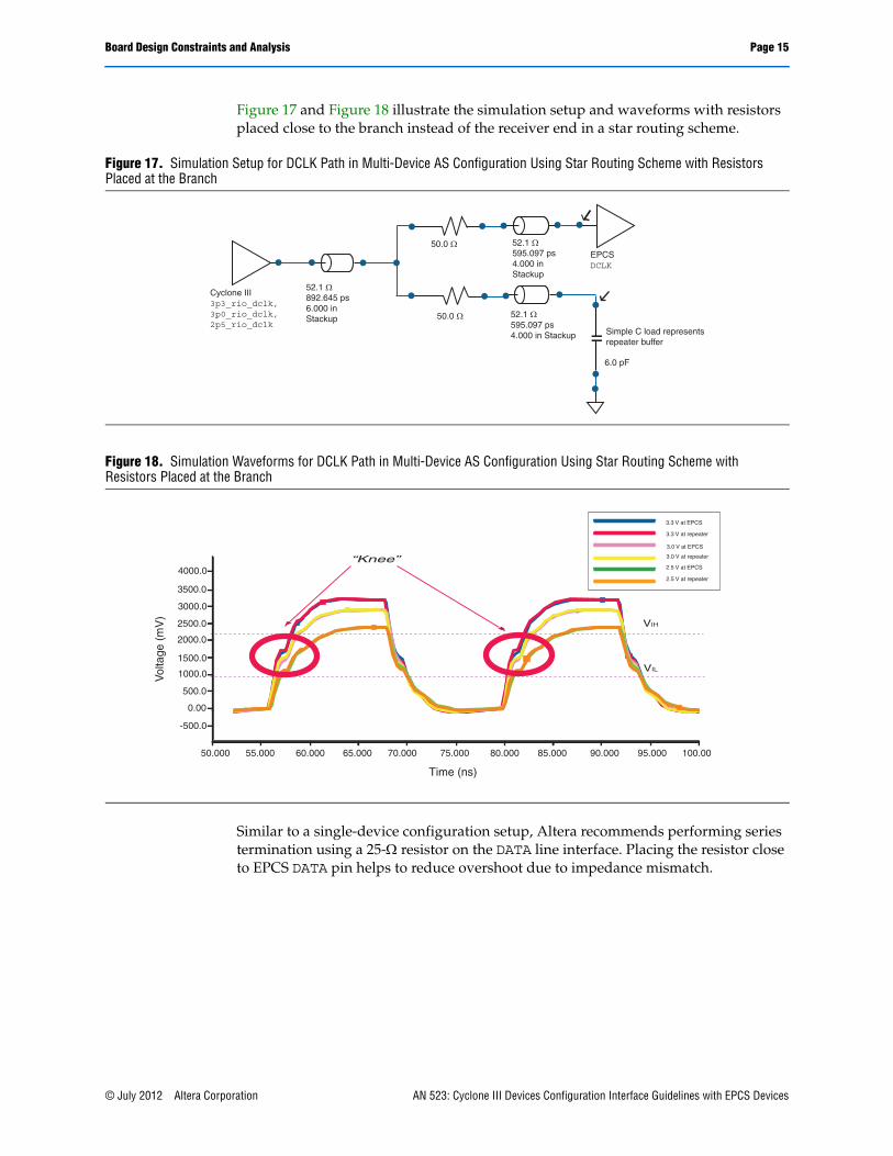
Placing resistors close to the branch does not help the monotonic transitions. While it matches the impedance mismatch at the branch position of the transmission path, the voltage drop across the resistors results in a "knee" during transition on the signal seen at each receiver end.
Figure 16. Simulation Waveforms for DCLK Path in Multi-Device AS Configuration Using Daisy Chain Routing Scheme Without Recommended Resistors
Time (ns)
Vol
tage
(m
V)
-500.0
500.0
1500.0
2500.0
3500.0
50.000 55.000 60.000 65.000 70.000 75.000 80.000 85.000 90.000 95.000 100.00
3000.0
2000.0
1000.0
4000.0
0.00
VIH
VIL
3.3 V at EPCS
3.3 V at repeater
3.0 V at EPCS
3.0 V at repeater
2.5 V at EPCS
2.5 V at repeater
AN 523: Cyclone III Devices Configuration Interface Guidelines with EPCS Devices © July 2012 Altera Corporation
Board Design Constraints and Analysis Page 15
Figure 17 and Figure 18 illustrate the simulation setup and waveforms with resistors placed close to the branch instead of the receiver end in a star routing scheme.
Similar to a single-device configuration setup, Altera recommends performing series termination using a 25- resistor on the DATA line interface. Placing the resistor close to EPCS DATA pin helps to reduce overshoot due to impedance mismatch.
Figure 17. Simulation Setup for DCLK Path in Multi-Device AS Configuration Using Star Routing Scheme with Resistors Placed at the Branch
Figure 18. Simulation Waveforms for DCLK Path in Multi-Device AS Configuration Using Star Routing Scheme with Resistors Placed at the Branch
Cyclone III3p3_rio_dclk, 3p0_rio_dclk, 2p5_rio_dclk
52.1 Ω892.645 ps6.000 inStackup
50.0 Ω
50.0 Ω
EPCSDCLK
6.0 pF
Simple C load represents repeater buffer
52.1 Ω595.097 ps4.000 in Stackup
52.1 Ω595.097 ps4.000 in Stackup
“Knee”
Time (ns)
Vol
tage
(m
V)
-500.0
500.0
1500.0
2500.0
3500.0
50.000 55.000 60.000 65.000 70.000 75.000 80.000 85.000 90.000 95.000 100.00
3000.0
2000.0
1000.0
4000.0
0.00
VIH
VIL
3.3 V at EPCS
3.3 V at repeater
3.0 V at EPCS
3.0 V at repeater
2.5 V at EPCS
2.5 V at repeater
© July 2012 Altera Corporation AN 523: Cyclone III Devices Configuration Interface Guidelines with EPCS Devices

Page 16 Board Design Constraints and Analysis
In-System Programming of EPCS Devices The in-system programmability feature allows direct programming access to the EPCS device without removing it from the system (with FPGA) using USB-Blaster™ or ByteBlaster™ II download cable. During in-system programming, the download cable disables the FPGA device access to the AS interface by driving the nCE pin high. Therefore, all AS output pins from the FPGA device are tristated.
1 Supply 3.3 V to the VCC(TRGT)pin of the download cables when you program the EPCS device.
f For more information on the correct VCC(TRGT) pin voltage requirements for the device being programmed, refer to the specifications section in USB-Blaster Download Cable User Guide or ByteBlaster II Download Cable User Guide.
Figure 19 illustrates the recommended setup for in-system programming of the EPCS device with Cyclone III family devices.
Figure 19. In-System Programming of EPCS Device Recommended Setup
nSTATUS
nCONFIGCONF_DONE
nCE
DATA[0] (7)DCLK (7)FLASH_nCE (5)DATA[1] (5)
nCEO
MSEL[3..0] (4)
Cyclone III Device
DATADCLK
nCSASDI
SerialConfiguration Device
GND
GND
N.C. (2)
VCCIO (1) VCCIO (1) VCCIO (1)
3.3 V (3)
GND
Pin 1
ByteBlaster II or USB Blaster10-Pin Male Header
3.3 V
10 pf
GND
GND
10 pf
(6)
10 pf
GND
10 pf
GND
(6)
10 ΩΩ 10 ΩΩ 10 ΩΩ
10 kΩ
3.3 V
3.3 V
3.3 V
AN 523: Cyclone III Devices Configuration Interface Guidelines with EPCS Devices © July 2012 Altera Corporation

Board Design Constraints and Analysis Page 17
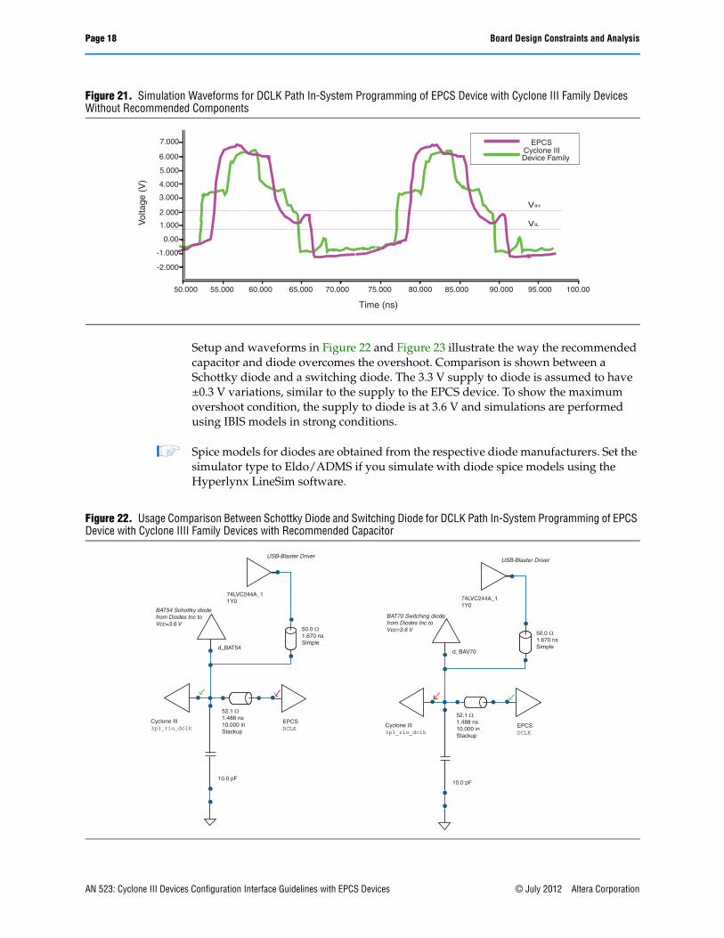
During in-system programming, even though all four AS pins from Cyclone III family devices are tristated, the pins must meet the maximum allowed input overshoot specification. Altera recommends using Schottky diodes to 3.3 V with 10 pF capacitors to limit the overshoot to an acceptable level on each Cyclone III family devices AS interface pins during in-system programming.
Figure 20 and Figure 21 illustrate the setup and simulation waveforms respectively for an example of overshoot at the DCLK pin of the Cyclone III device duringin-system programming with the USB-Blaster download cable without the recommended components. The USB-Blaster download cable uses the Philips 74LVC244A octal buffer or line driver chip. To show the maximum overshoot, simulations are performed using the IBIS models in strong (best) conditions (strongest process corner, high voltage, and low temperature). The resulting overshoot violates the maximum overshoot specification and puts Cyclone III family devices at reliability risk.
Notes to Figure 19:
(1) Connect these pull-up resistors to the VCCIO supply of the bank in which the pin resides.(2) The nCEO pin can be left unconnected or used as a user I/O pin when it does not feed the nCE pin of another device.(3) Power up the ByteBlaster II or USB-Blaster cable’s VCC with the 3.3-V supply.(4) The MSEL pin settings vary for different configuration voltage standards and power-on reset (POR) time. To connect
MSEL[3..0], refer to Configuration, Design Security, and Remote System Upgrades in Cyclone III Devices chapter in volume 1 of the Cyclone III Device Handbook. Connect the MSEL pins directly to VCCA or ground.
(5) These are dual-purpose I/O pins. The FLASH_nCE pin functions as the nCSO pin in the AS configuration scheme. The DATA[1] pin functions as the ASDO pin in the AS configuration scheme.
(6) The diodes and capacitors must be placed as close as possible to the Cyclone III device. You must ensure the diodes and capacitors maintain a maximum AC voltage of 4.1 V. The external diodes and capacitors are required to prevent damage to the Cyclone III AS configuration input pins due to possible overshoot when programming the serial configuration device using a download cable. Altera recommends using the Schottky diode, which has a relatively lower forward diode voltage (VF) than the switching and Zener diodes, for effective voltage clamping.
(7) When cascading Cyclone III devices in a multi-device AS configuration, connect the repeater buffers between the Cyclone III master and slave device or devices for DATA[0] and DCLK. All I/O inputs must maintain a maximum AC voltage of 4.1 V. The output resistance of the repeater buffers must fit the maximum overshoot equation outlined in Configuration and JTAG Pin I/O Requirements section in Configuration, Design Security, and Remote System Upgrades in Cyclone III Devices chapter in volume 1 of the Cyclone III Device Handbook.
Figure 19. In-System Programming of EPCS Device Recommended Setup
Figure 20. Simulation Setup for DCLK Path In-System Programming of EPCS Device with Cyclone III Family Devices Without Recommended Components
USB-Blaster Driver
74LVC244A_11Y0
50.0 Ω1.670 nsSimple
Cyclone III3p3_rio_dclk
52.1 Ω1.488 ns10.000 inStackup
EPCSDCLK
© July 2012 Altera Corporation AN 523: Cyclone III Devices Configuration Interface Guidelines with EPCS Devices
Page 18 Board Design Constraints and Analysis
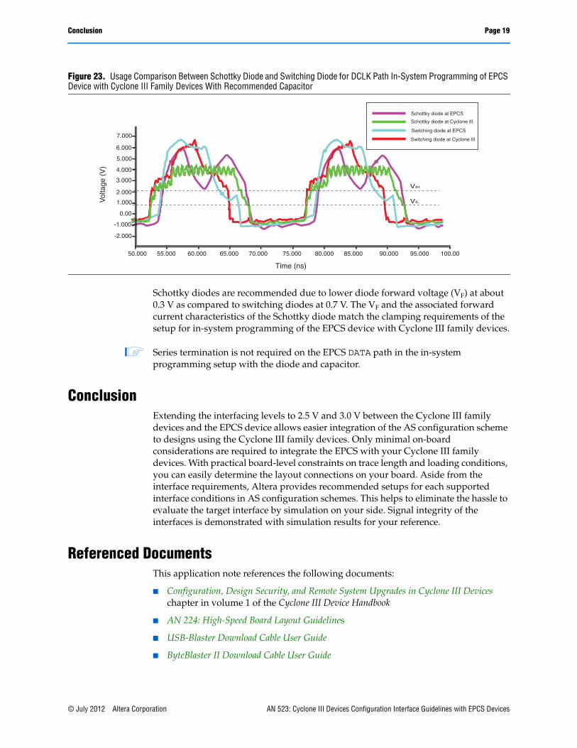
Setup and waveforms in Figure 22 and Figure 23 illustrate the way the recommended capacitor and diode overcomes the overshoot. Comparison is shown between a Schottky diode and a switching diode. The 3.3 V supply to diode is assumed to have ±0.3 V variations, similar to the supply to the EPCS device. To show the maximum overshoot condition, the supply to diode is at 3.6 V and simulations are performed using IBIS models in strong conditions.
1 Spice models for diodes are obtained from the respective diode manufacturers. Set the simulator type to Eldo/ADMS if you simulate with diode spice models using the Hyperlynx LineSim software.
Figure 21. Simulation Waveforms for DCLK Path In-System Programming of EPCS Device with Cyclone III Family Devices Without Recommended Components
Time (ns)
Vol
tage
(V
)
-2.000
0.00
2.000
4.000
6.000
50.000 55.000 60.000 65.000 70.000 75.000 80.000 85.000 90.000 95.000 100.00
5.000
3.000
1.000
7.000
-1.000
EPCS
VIH
VIL
Cyclone III Device Family
Figure 22. Usage Comparison Between Schottky Diode and Switching Diode for DCLK Path In-System Programming of EPCS Device with Cyclone IIII Family Devices with Recommended Capacitor
USB-Blaster Driver
74LVC244A_11Y0
50.0 Ω1.670 nsSimple
Cyclone III3p3_rio_dclk
52.1 Ω1.488 ns10.000 inStackup
EPCSDCLK
BAT54 Schottky diode from Diodes Inc to Vcc=3.6 V
d_BAT54
10.0 pF
USB-Blaster Driver
74LVC244A_11Y0
50.0 Ω1.670 nsSimple
Cyclone III3p3_rio_dclk
52.1 Ω1.488 ns10.000 inStackup
EPCSDCLK
BAT70 Switching diode from Diodes Inc to Vcc=3.6 V
d_BAV70
10.0 pF
AN 523: Cyclone III Devices Configuration Interface Guidelines with EPCS Devices © July 2012 Altera Corporation
Conclusion Page 19
Schottky diodes are recommended due to lower diode forward voltage (VF) at about 0.3 V as compared to switching diodes at 0.7 V. The VF and the associated forward current characteristics of the Schottky diode match the clamping requirements of the setup for in-system programming of the EPCS device with Cyclone III family devices.
1 Series termination is not required on the EPCS DATA path in the in-system programming setup with the diode and capacitor.
ConclusionExtending the interfacing levels to 2.5 V and 3.0 V between the Cyclone III family devices and the EPCS device allows easier integration of the AS configuration scheme to designs using the Cyclone III family devices. Only minimal on-board considerations are required to integrate the EPCS with your Cyclone III family devices. With practical board-level constraints on trace length and loading conditions, you can easily determine the layout connections on your board. Aside from the interface requirements, Altera provides recommended setups for each supported interface conditions in AS configuration schemes. This helps to eliminate the hassle to evaluate the target interface by simulation on your side. Signal integrity of the interfaces is demonstrated with simulation results for your reference.
Referenced DocumentsThis application note references the following documents:
■ Configuration, Design Security, and Remote System Upgrades in Cyclone III Devices chapter in volume 1 of the Cyclone III Device Handbook
■ AN 224: High-Speed Board Layout Guidelines
■ USB-Blaster Download Cable User Guide
■ ByteBlaster II Download Cable User Guide
Figure 23. Usage Comparison Between Schottky Diode and Switching Diode for DCLK Path In-System Programming of EPCS Device with Cyclone III Family Devices With Recommended Capacitor
Time (ns)
Vol
tage
(V
)
-2.000
0.00
2.000
4.000
6.000
50.000 55.000 60.000 65.000 70.000 75.000 80.000 85.000 90.000 95.000 100.00
5.000
3.000
1.000
7.000
-1.000
VIH
VIL
Schottky diode at Cyclone III
Switching diode at EPCS
Switching diode at Cyclone III
Schottky diode at EPCS
© July 2012 Altera Corporation AN 523: Cyclone III Devices Configuration Interface Guidelines with EPCS Devices

101 Innovation DriveSan Jose, CA 95134www.altera.comTechnical Supportwww.altera.com/support
Copyright © 2012 Altera Corporation. All rights reserved. Altera, The Programmable Solutions Company, the stylized Altera logo, specific device designations, and all other words and logos that are identified as trademarks and/or service marks are, unless noted otherwise, the trademarks and service marks of Altera Corporation in the U.S. and other countries. All other product or service names are the property of their respective holders. Altera products are protected under numerous U.S. and foreign patents and pending applications, maskwork rights, and copyrights. Altera warrants performance of its semiconductor products to current specifications in accordance with Altera's standard warranty, but reserves the right to make changes to any products and services at any time without notice. Altera assumes no responsibility or liability arising out of the application or use of any information, product, or service described herein except as expressly agreed to in writing by Altera Corporation. Altera customers are advised to obtain the latest version of device specifications before relying on any published information and before placing orders for products or services.
Document Revision HistoryTable 4 shows the revision history for this application note.
Table 4. Document Revision History
Date and Document Version Changes Made Summary of Changes
July 2012 v1.2 ■ Updated links to the Configuration, Design Security, and Remote System Upgrades in Cyclone III Devices chapter.
—
June 2009 v1.1. ■ Updated title to “AN 523: Cyclone III Devices Configuration Interface Guidelines with EPCS Devices” on page 1.
■ Updated “Introduction” on page 1.
■ Updated “AS Interfacing Overview” on page 1.
■ Updated “Electrical Specification Compatibility” on page 2.
■ Updated Table 1 on page 3 and Table 3 on page 5.
■ Updated “Board Design Constraints and Analysis” on page 5.
■ Updated Figure 3 on page 7, Figure 8 on page 10, and Figure 19 on page 16.
■ Updated “Multi-Device AS Configuration” on page 9.
■ Updated “Conclusion” on page 19.
■ Updated “Referenced Documents” on page 19.
Updated to include Cyclone III LS information.
June 2008 v1.0 Initial release. —