Cyclone III Device Handbook Volume 2. Chapter 1. Cyclone ... · Cyclone III devices. Operating...
34
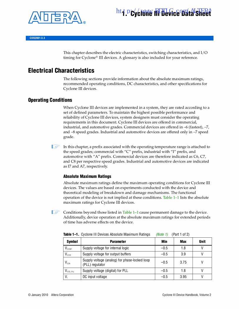
© January 2010 Altera Corporation Cyclone III Device Handbook, Volume 2 1. Cyclone III Device Data Sheet This chapter describes the electric characteristics, switching characteristics, and I/O timing for Cyclone ® III devices. A glossary is also included for your reference. Electrical Characteristics The following sections provide information about the absolute maximum ratings, recommended operating conditions, DC characteristics, and other specifications for Cyclone III devices. Operating Conditions When Cyclone III devices are implemented in a system, they are rated according to a set of defined parameters. To maintain the highest possible performance and reliability of Cyclone III devices, system designers must consider the operating requirements in this document. Cyclone III devices are offered in commercial, industrial, and automotive grades. Commercial devices are offered in –6 (fastest), –7, and –8 speed grades. Industrial and automotive devices are offered only in –7 speed grade. 1 In this chapter, a prefix associated with the operating temperature range is attached to the speed grades; commercial with “C” prefix, industrial with “I” prefix, and automotive with “A” prefix. Commercial devices are therefore indicated as C6, C7, and C8 per respective speed grades. Industrial and automotive devices are indicated as I7 and A7, respectively. Absolute Maximum Ratings Absolute maximum ratings define the maximum operating conditions for Cyclone III devices. The values are based on experiments conducted with the device and theoretical modeling of breakdown and damage mechanisms. The functional operation of the device is not implied at these conditions. Table 1–1 lists the absolute maximum ratings for Cyclone III devices. 1 Conditions beyond those listed in Table 1–1 cause permanent damage to the device. Additionally, device operation at the absolute maximum ratings for extended periods of time has adverse effects on the device. Table 1–1. Cyclone III Devices Absolute Maximum Ratings (Note 1) (Part 1 of 2) Symbol Parameter Min Max Unit V CCINT Supply voltage for internal logic –0.5 1.8 V VCCIO Supply voltage for output buffers –0.5 3.9 V V CCA Supply voltage (analog) for phase-locked loop (PLL) regulator –0.5 3.75 V V CCD_PLL Supply voltage (digital) for PLL –0.5 1.8 V VI DC input voltage –0.5 3.95 V CIII52001-3.3 http://www.BDTIC.com/ALTERA
Transcript of Cyclone III Device Handbook Volume 2. Chapter 1. Cyclone ... · Cyclone III devices. Operating...
© January 2010 Altera Corporation Cyclone III Device Handbook, Volume 2
1. Cyclone III Device Data Sheet
This chapter describes the electric characteristics, switching characteristics, and I/O timing for Cyclone® III devices. A glossary is also included for your reference.
Electrical CharacteristicsThe following sections provide information about the absolute maximum ratings, recommended operating conditions, DC characteristics, and other specifications for Cyclone III devices.
Operating ConditionsWhen Cyclone III devices are implemented in a system, they are rated according to a set of defined parameters. To maintain the highest possible performance and reliability of Cyclone III devices, system designers must consider the operating requirements in this document. Cyclone III devices are offered in commercial, industrial, and automotive grades. Commercial devices are offered in –6 (fastest), –7, and –8 speed grades. Industrial and automotive devices are offered only in –7 speed grade.
1 In this chapter, a prefix associated with the operating temperature range is attached to the speed grades; commercial with “C” prefix, industrial with “I” prefix, and automotive with “A” prefix. Commercial devices are therefore indicated as C6, C7, and C8 per respective speed grades. Industrial and automotive devices are indicated as I7 and A7, respectively.
Absolute Maximum RatingsAbsolute maximum ratings define the maximum operating conditions for Cyclone III devices. The values are based on experiments conducted with the device and theoretical modeling of breakdown and damage mechanisms. The functional operation of the device is not implied at these conditions. Table 1–1 lists the absolute maximum ratings for Cyclone III devices.
1 Conditions beyond those listed in Table 1–1 cause permanent damage to the device. Additionally, device operation at the absolute maximum ratings for extended periods of time has adverse effects on the device.
Table 1–1. Cyclone III Devices Absolute Maximum Ratings (Note 1) (Part 1 of 2)
Symbol Parameter Min Max Unit
VCCINT Supply voltage for internal logic –0.5 1.8 V
VCCIO Supply voltage for output buffers –0.5 3.9 V
VCCA
Supply voltage (analog) for phase-locked loop (PLL) regulator
–0.5 3.75 V
VCCD_PLL Supply voltage (digital) for PLL –0.5 1.8 V
VI DC input voltage –0.5 3.95 V
CIII52001-3.3
http://www.BDTIC.com/ALTERA
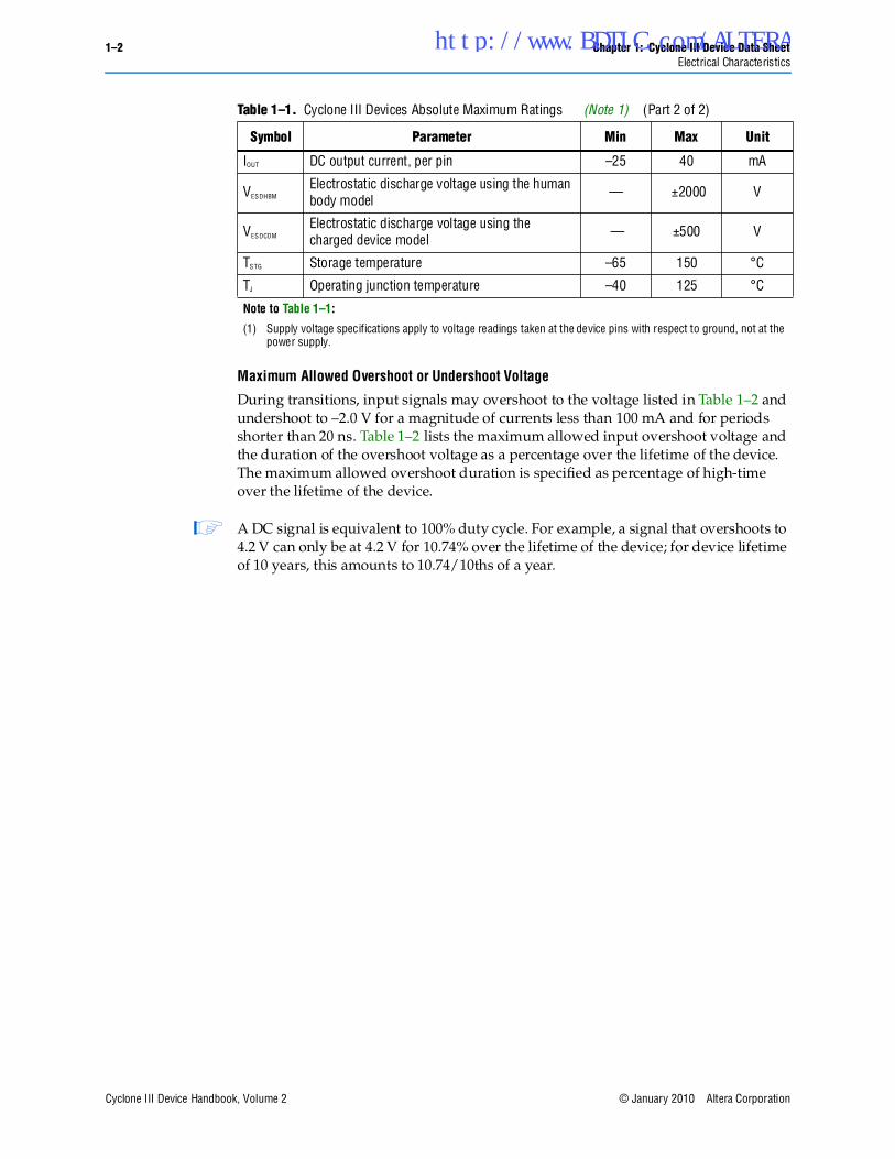
1–2 Chapter 1: Cyclone III Device Data SheetElectrical Characteristics
Cyclone III Device Handbook, Volume 2 © January 2010 Altera Corporation
Maximum Allowed Overshoot or Undershoot Voltage
During transitions, input signals may overshoot to the voltage listed in Table 1–2 and undershoot to –2.0 V for a magnitude of currents less than 100 mA and for periods shorter than 20 ns. Table 1–2 lists the maximum allowed input overshoot voltage and the duration of the overshoot voltage as a percentage over the lifetime of the device. The maximum allowed overshoot duration is specified as percentage of high-time over the lifetime of the device.
1 A DC signal is equivalent to 100% duty cycle. For example, a signal that overshoots to 4.2 V can only be at 4.2 V for 10.74% over the lifetime of the device; for device lifetime of 10 years, this amounts to 10.74/10ths of a year.
IOUT DC output current, per pin –25 40 mA
VESDHBM
Electrostatic discharge voltage using the human body model
— ±2000 V
VESDCDM
Electrostatic discharge voltage using the charged device model
— ±500 V
TSTG Storage temperature –65 150 °C
TJ Operating junction temperature –40 125 °C
Note to Table 1–1:
(1) Supply voltage specifications apply to voltage readings taken at the device pins with respect to ground, not at the power supply.
Table 1–1. Cyclone III Devices Absolute Maximum Ratings (Note 1) (Part 2 of 2)
Symbol Parameter Min Max Unit
http://www.BDTIC.com/ALTERA
Chapter 1: Cyclone III Device Data Sheet 1–3Electrical Characteristics
© January 2010 Altera Corporation Cyclone III Device Handbook, Volume 2
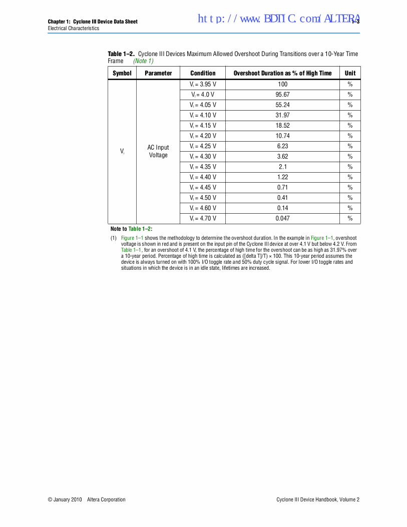
Table 1–2. Cyclone III Devices Maximum Allowed Overshoot During Transitions over a 10-Year Time Frame (Note 1)
Symbol Parameter Condition Overshoot Duration as % of High Time Unit
Vi
AC Input Voltage
VI = 3.95 V 100 %
VI = 4.0 V 95.67 %
VI = 4.05 V 55.24 %
VI = 4.10 V 31.97 %
VI = 4.15 V 18.52 %
VI = 4.20 V 10.74 %
VI = 4.25 V 6.23 %
VI = 4.30 V 3.62 %
VI = 4.35 V 2.1 %
VI = 4.40 V 1.22 %
VI = 4.45 V 0.71 %
VI = 4.50 V 0.41 %
VI = 4.60 V 0.14 %
VI = 4.70 V 0.047 %
Note to Table 1–2:
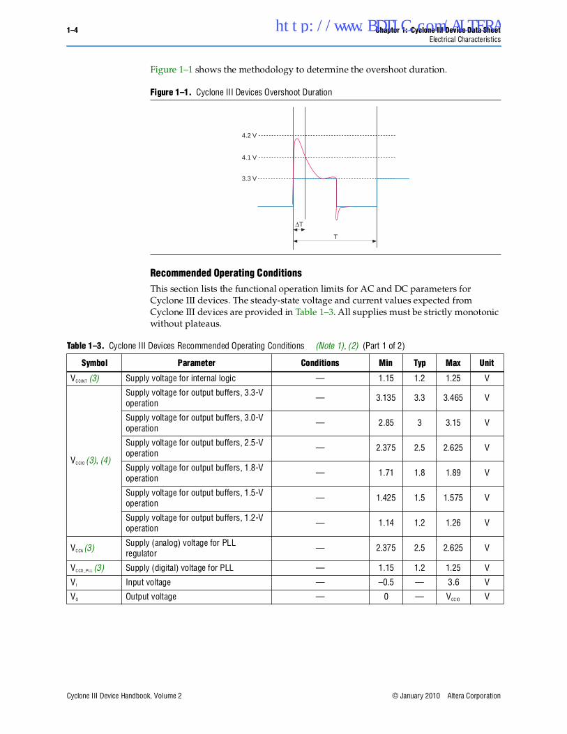
(1) Figure 1–1 shows the methodology to determine the overshoot duration. In the example in Figure 1–1, overshoot voltage is shown in red and is present on the input pin of the Cyclone III device at over 4.1 V but below 4.2 V. From Table 1–1, for an overshoot of 4.1 V, the percentage of high time for the overshoot can be as high as 31.97% over a 10-year period. Percentage of high time is calculated as ([delta T]/T) × 100. This 10-year period assumes the device is always turned on with 100% I/O toggle rate and 50% duty cycle signal. For lower I/O toggle rates and situations in which the device is in an idle state, lifetimes are increased.
http://www.BDTIC.com/ALTERA
1–4 Chapter 1: Cyclone III Device Data SheetElectrical Characteristics
Cyclone III Device Handbook, Volume 2 © January 2010 Altera Corporation
Figure 1–1 shows the methodology to determine the overshoot duration.
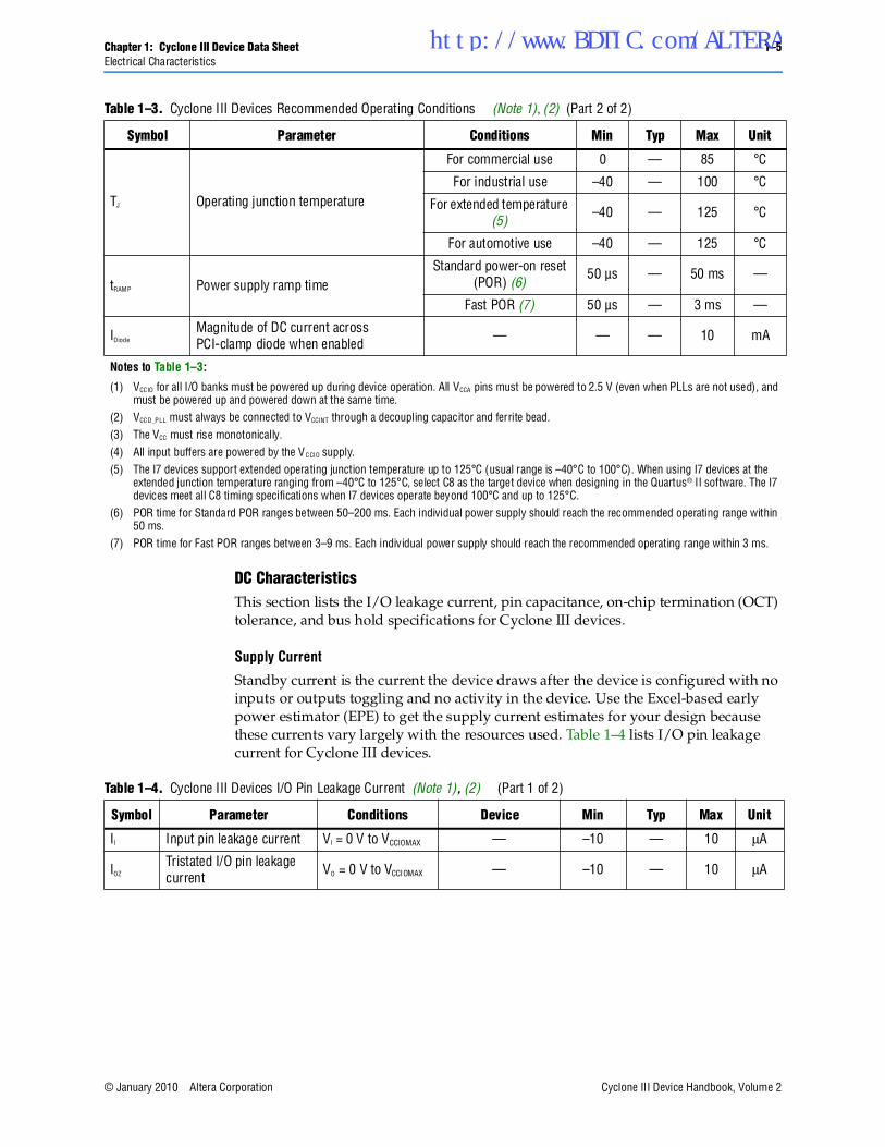
Recommended Operating ConditionsThis section lists the functional operation limits for AC and DC parameters for Cyclone III devices. The steady-state voltage and current values expected from Cyclone III devices are provided in Table 1–3. All supplies must be strictly monotonic without plateaus.
Figure 1–1. Cyclone III Devices Overshoot Duration
3.3 V
4.1 V
4.2 V
T
ΔT
Table 1–3. Cyclone III Devices Recommended Operating Conditions (Note 1), (2) (Part 1 of 2)
Symbol Parameter Conditions Min Typ Max Unit
VCCINT (3) Supply voltage for internal logic — 1.15 1.2 1.25 V
VCCIO (3), (4)
Supply voltage for output buffers, 3.3-V operation
— 3.135 3.3 3.465 V
Supply voltage for output buffers, 3.0-V operation
— 2.85 3 3.15 V
Supply voltage for output buffers, 2.5-V operation
— 2.375 2.5 2.625 V
Supply voltage for output buffers, 1.8-V operation
— 1.71 1.8 1.89 V
Supply voltage for output buffers, 1.5-V operation
— 1.425 1.5 1.575 V
Supply voltage for output buffers, 1.2-V operation
— 1.14 1.2 1.26 V
VCCA (3) Supply (analog) voltage for PLL regulator
— 2.375 2.5 2.625 V
VCCD_PLL (3) Supply (digital) voltage for PLL — 1.15 1.2 1.25 V
VI Input voltage — –0.5 — 3.6 V
VO Output voltage — 0 — VCCIO V
http://www.BDTIC.com/ALTERA
Chapter 1: Cyclone III Device Data Sheet 1–5Electrical Characteristics
© January 2010 Altera Corporation Cyclone III Device Handbook, Volume 2
DC CharacteristicsThis section lists the I/O leakage current, pin capacitance, on-chip termination (OCT) tolerance, and bus hold specifications for Cyclone III devices.
Supply Current
Standby current is the current the device draws after the device is configured with no inputs or outputs toggling and no activity in the device. Use the Excel-based early power estimator (EPE) to get the supply current estimates for your design because these currents vary largely with the resources used. Table 1–4 lists I/O pin leakage current for Cyclone III devices.
TJ Operating junction temperature
For commercial use 0 — 85 °C
For industrial use –40 — 100 °C
For extended temperature (5)
–40 — 125 °C
For automotive use –40 — 125 °C
tRAMP Power supply ramp timeStandard power-on reset
(POR) (6)50 µs — 50 ms —
Fast POR (7) 50 µs — 3 ms —
IDiode
Magnitude of DC current across PCI-clamp diode when enabled
— — — 10 mA
Notes to Table 1–3:
(1) VCCIO for all I/O banks must be powered up during device operation. All VCCA pins must be powered to 2.5 V (even when PLLs are not used), and must be powered up and powered down at the same time.
(2) VCCD_PLL must always be connected to VCCINT through a decoupling capacitor and ferrite bead.(3) The VCC must rise monotonically.(4) All input buffers are powered by the VCCIO supply.(5) The I7 devices support extended operating junction temperature up to 125°C (usual range is –40°C to 100°C). When using I7 devices at the
extended junction temperature ranging from –40°C to 125°C, select C8 as the target device when designing in the Quartus® II software. The I7 devices meet all C8 timing specifications when I7 devices operate beyond 100°C and up to 125°C.
(6) POR time for Standard POR ranges between 50–200 ms. Each individual power supply should reach the recommended operating range within 50 ms.
(7) POR time for Fast POR ranges between 3–9 ms. Each individual power supply should reach the recommended operating range within 3 ms.
Table 1–3. Cyclone III Devices Recommended Operating Conditions (Note 1), (2) (Part 2 of 2)
Symbol Parameter Conditions Min Typ Max Unit
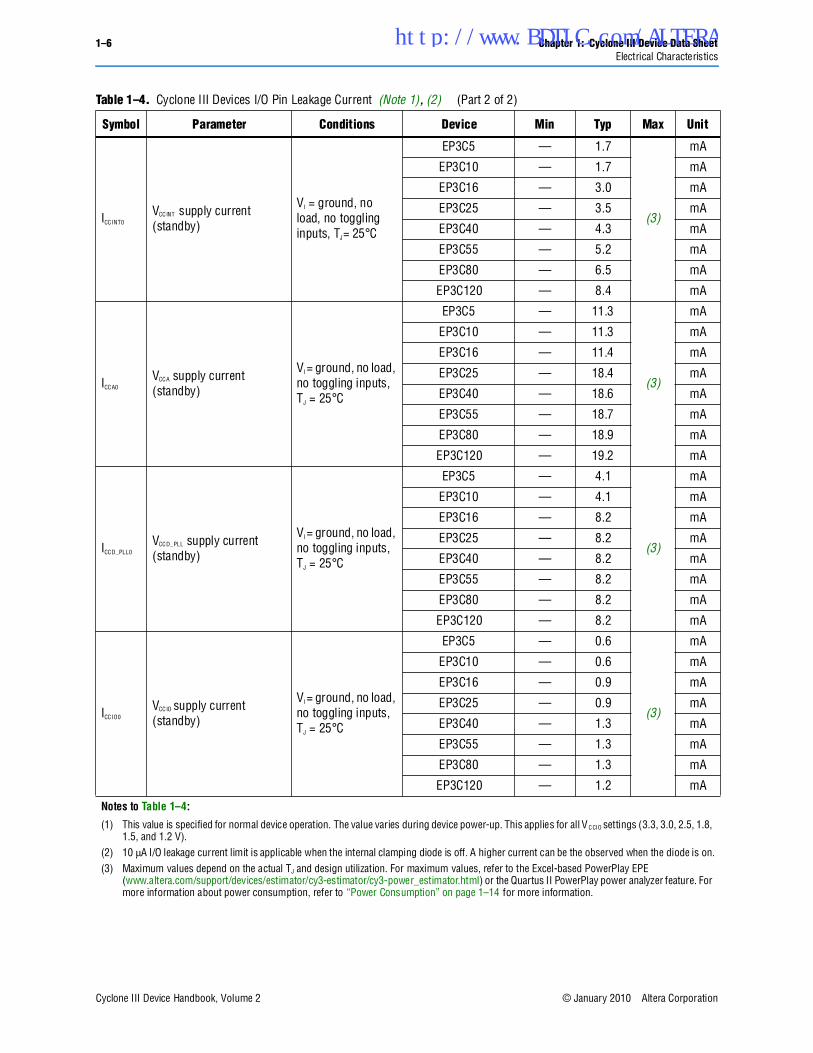
Table 1–4. Cyclone III Devices I/O Pin Leakage Current (Note 1), (2) (Part 1 of 2)
Symbol Parameter Conditions Device Min Typ Max Unit
II Input pin leakage current VI = 0 V to VCCIOMAX — –10 — 10 μA
IOZ
Tristated I/O pin leakage current
VO = 0 V to VCCIOMAX — –10 — 10 μA
http://www.BDTIC.com/ALTERA
1–6 Chapter 1: Cyclone III Device Data SheetElectrical Characteristics
Cyclone III Device Handbook, Volume 2 © January 2010 Altera Corporation
ICCINT0
VCCINT supply current (standby)
VI = ground, no load, no toggling inputs, TJ= 25°C
EP3C5 — 1.7
(3)
mA
EP3C10 — 1.7 mA
EP3C16 — 3.0 mA
EP3C25 — 3.5 mA
EP3C40 — 4.3 mA
EP3C55 — 5.2 mA
EP3C80 — 6.5 mA
EP3C120 — 8.4 mA
ICCA0
VCCA supply current (standby)
VI = ground, no load, no toggling inputs, TJ = 25°C
EP3C5 — 11.3
(3)
mA
EP3C10 — 11.3 mA
EP3C16 — 11.4 mA
EP3C25 — 18.4 mA
EP3C40 — 18.6 mA
EP3C55 — 18.7 mA
EP3C80 — 18.9 mA
EP3C120 — 19.2 mA
ICCD_PLL0
VCCD_PLL supply current (standby)
VI = ground, no load, no toggling inputs, TJ = 25°C
EP3C5 — 4.1
(3)
mA
EP3C10 — 4.1 mA
EP3C16 — 8.2 mA
EP3C25 — 8.2 mA
EP3C40 — 8.2 mA
EP3C55 — 8.2 mA
EP3C80 — 8.2 mA
EP3C120 — 8.2 mA
ICCIO0
VCCIO supply current (standby)
VI = ground, no load, no toggling inputs, TJ = 25°C
EP3C5 — 0.6
(3)
mA
EP3C10 — 0.6 mA
EP3C16 — 0.9 mA
EP3C25 — 0.9 mA
EP3C40 — 1.3 mA
EP3C55 — 1.3 mA
EP3C80 — 1.3 mA
EP3C120 — 1.2 mA
Notes to Table 1–4:
(1) This value is specified for normal device operation. The value varies during device power-up. This applies for all VCCIO settings (3.3, 3.0, 2.5, 1.8, 1.5, and 1.2 V).
(2) 10 μA I/O leakage current limit is applicable when the internal clamping diode is off. A higher current can be the observed when the diode is on.(3) Maximum values depend on the actual TJ and design utilization. For maximum values, refer to the Excel-based PowerPlay EPE
(www.altera.com/support/devices/estimator/cy3-estimator/cy3-power_estimator.html) or the Quartus II PowerPlay power analyzer feature. For more information about power consumption, refer to “Power Consumption” on page 1–14 for more information.
Table 1–4. Cyclone III Devices I/O Pin Leakage Current (Note 1), (2) (Part 2 of 2)
Symbol Parameter Conditions Device Min Typ Max Unit
http://www.BDTIC.com/ALTERA
Chapter 1: Cyclone III Device Data Sheet 1–7Electrical Characteristics
© January 2010 Altera Corporation Cyclone III Device Handbook, Volume 2
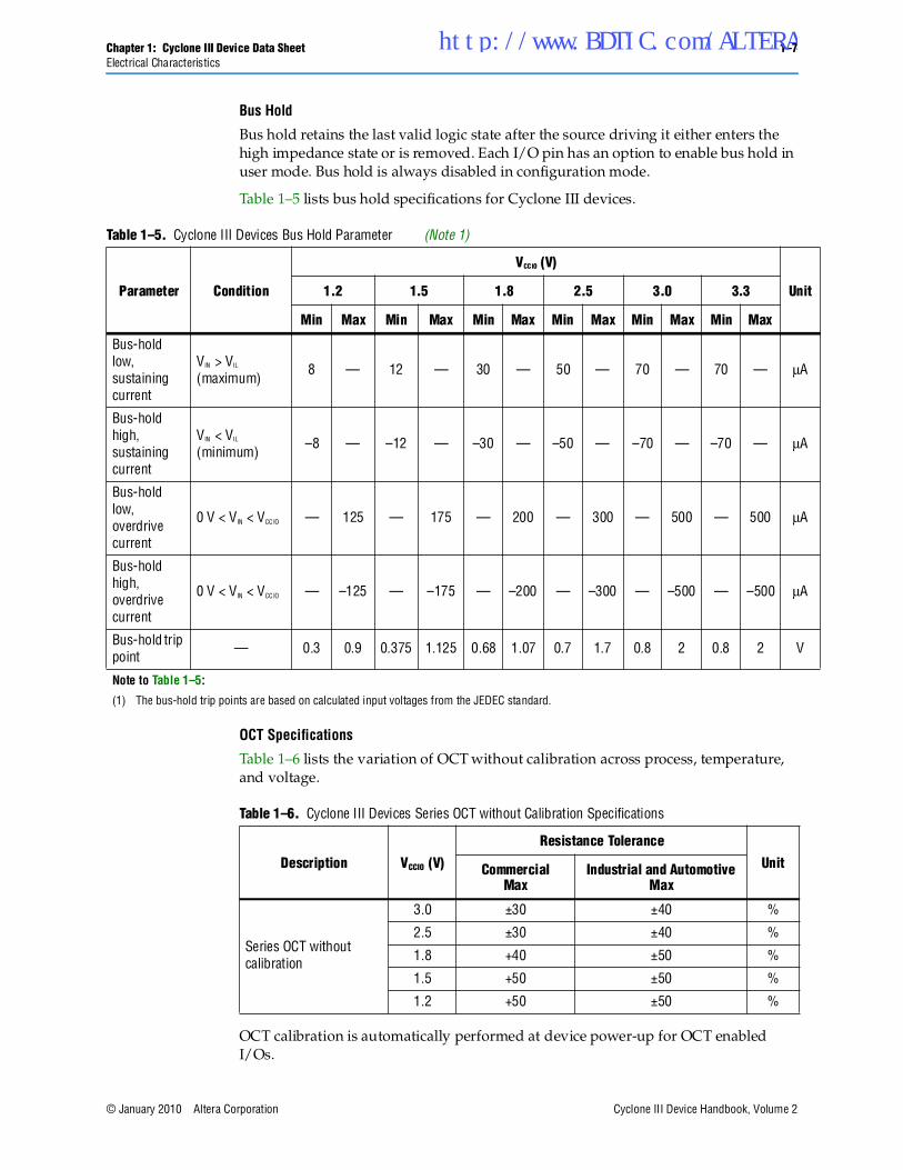
Bus Hold
Bus hold retains the last valid logic state after the source driving it either enters the high impedance state or is removed. Each I/O pin has an option to enable bus hold in user mode. Bus hold is always disabled in configuration mode.
Table 1–5 lists bus hold specifications for Cyclone III devices.
OCT Specifications
Table 1–6 lists the variation of OCT without calibration across process, temperature, and voltage.
OCT calibration is automatically performed at device power-up for OCT enabled I/Os.
Table 1–5. Cyclone III Devices Bus Hold Parameter (Note 1)
Parameter Condition
VCCIO (V)
Unit1.2 1.5 1.8 2.5 3.0 3.3
Min Max Min Max Min Max Min Max Min Max Min Max
Bus-hold low, sustaining current
VIN > VIL
(maximum)8 — 12 — 30 — 50 — 70 — 70 — μA
Bus-hold high, sustaining current
VIN < VIL
(minimum)–8 — –12 — –30 — –50 — –70 — –70 — μA
Bus-hold low, overdrive current
0 V < VIN < VCCIO — 125 — 175 — 200 — 300 — 500 — 500 μA
Bus-hold high, overdrive current
0 V < VIN < VCCIO — –125 — –175 — –200 — –300 — –500 — –500 μA
Bus-hold trip point
— 0.3 0.9 0.375 1.125 0.68 1.07 0.7 1.7 0.8 2 0.8 2 V
Note to Table 1–5:
(1) The bus-hold trip points are based on calculated input voltages from the JEDEC standard.
Table 1–6. Cyclone III Devices Series OCT without Calibration Specifications
Description VCCIO (V)
Resistance Tolerance
UnitCommercial Max
Industrial and Automotive Max
Series OCT without calibration
3.0 ±30 ±40 %
2.5 ±30 ±40 %
1.8 +40 ±50 %
1.5 +50 ±50 %
1.2 +50 ±50 %
http://www.BDTIC.com/ALTERA
1–8 Chapter 1: Cyclone III Device Data SheetElectrical Characteristics
Cyclone III Device Handbook, Volume 2 © January 2010 Altera Corporation
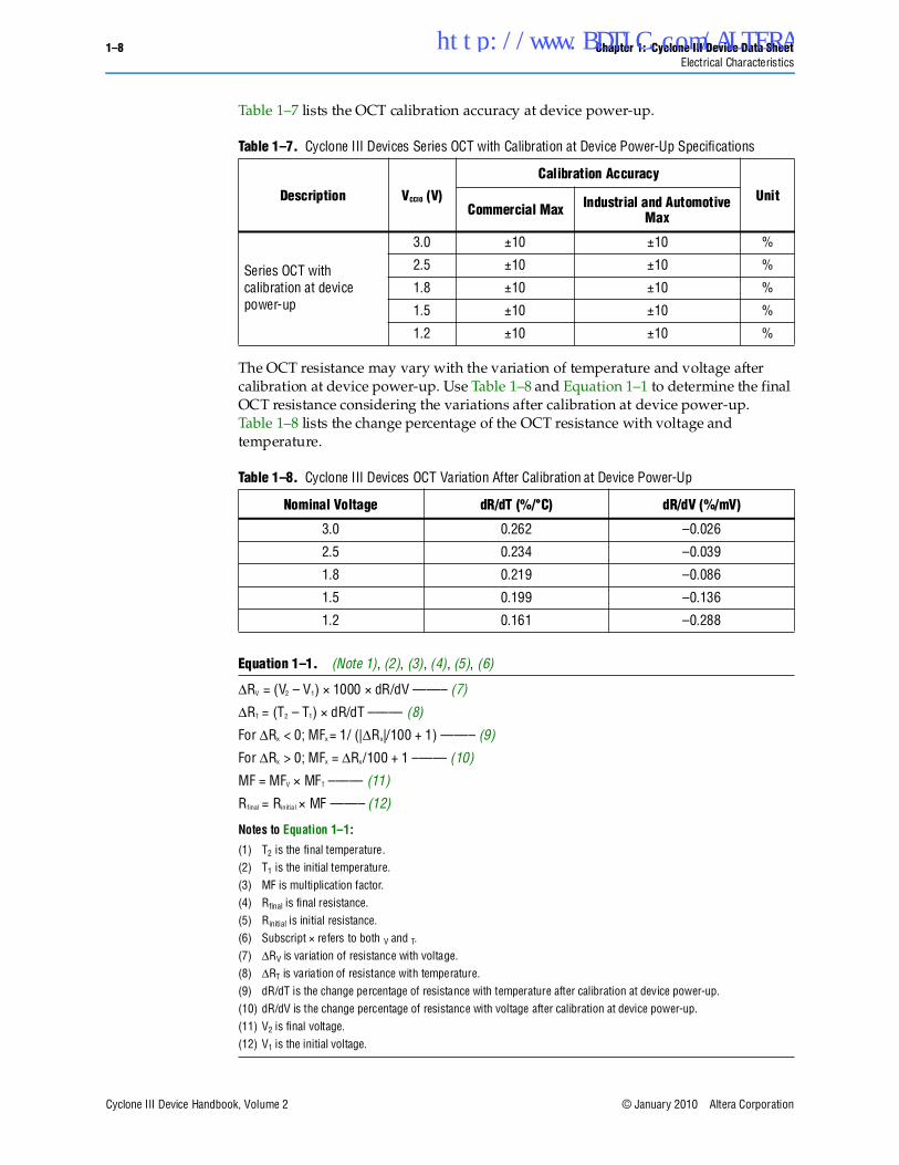
Table 1–7 lists the OCT calibration accuracy at device power-up.
The OCT resistance may vary with the variation of temperature and voltage after calibration at device power-up. Use Table 1–8 and Equation 1–1 to determine the final OCT resistance considering the variations after calibration at device power-up. Table 1–8 lists the change percentage of the OCT resistance with voltage and temperature.
Table 1–7. Cyclone III Devices Series OCT with Calibration at Device Power-Up Specifications
Description VCCIO (V)
Calibration Accuracy
UnitCommercial Max Industrial and Automotive
Max
Series OCT with calibration at device power-up
3.0 ±10 ±10 %
2.5 ±10 ±10 %
1.8 ±10 ±10 %
1.5 ±10 ±10 %
1.2 ±10 ±10 %
Table 1–8. Cyclone III Devices OCT Variation After Calibration at Device Power-Up
Nominal Voltage dR/dT (%/°C) dR/dV (%/mV)
3.0 0.262 –0.026
2.5 0.234 –0.039
1.8 0.219 –0.086
1.5 0.199 –0.136
1.2 0.161 –0.288
Equation 1–1. (Note 1), (2), (3), (4), (5), (6)
ΔRV = (V2 – V1) × 1000 × dR/dV ––––– (7)
ΔRT = (T2 – T1) × dR/dT ––––– (8)
For ΔRx < 0; MFx = 1/ (|ΔRx|/100 + 1) ––––– (9)
For ΔRx > 0; MFx = ΔRx/100 + 1 ––––– (10)
MF = MFV × MFT ––––– (11)
Rfinal = Rinitia l × MF ––––– (12)
Notes to Equation 1–1:
(1) T2 is the final temperature. (2) T1 is the initial temperature. (3) MF is multiplication factor. (4) Rfinal is final resistance. (5) Rinitial is initial resistance. (6) Subscript × refers to both V and T.(7) ΔRV is variation of resistance with voltage. (8) ΔRT is variation of resistance with temperature. (9) dR/dT is the change percentage of resistance with temperature after calibration at device power-up. (10) dR/dV is the change percentage of resistance with voltage after calibration at device power-up. (11) V2 is final voltage. (12) V1 is the initial voltage.
http://www.BDTIC.com/ALTERA
Chapter 1: Cyclone III Device Data Sheet 1–9Electrical Characteristics
© January 2010 Altera Corporation Cyclone III Device Handbook, Volume 2
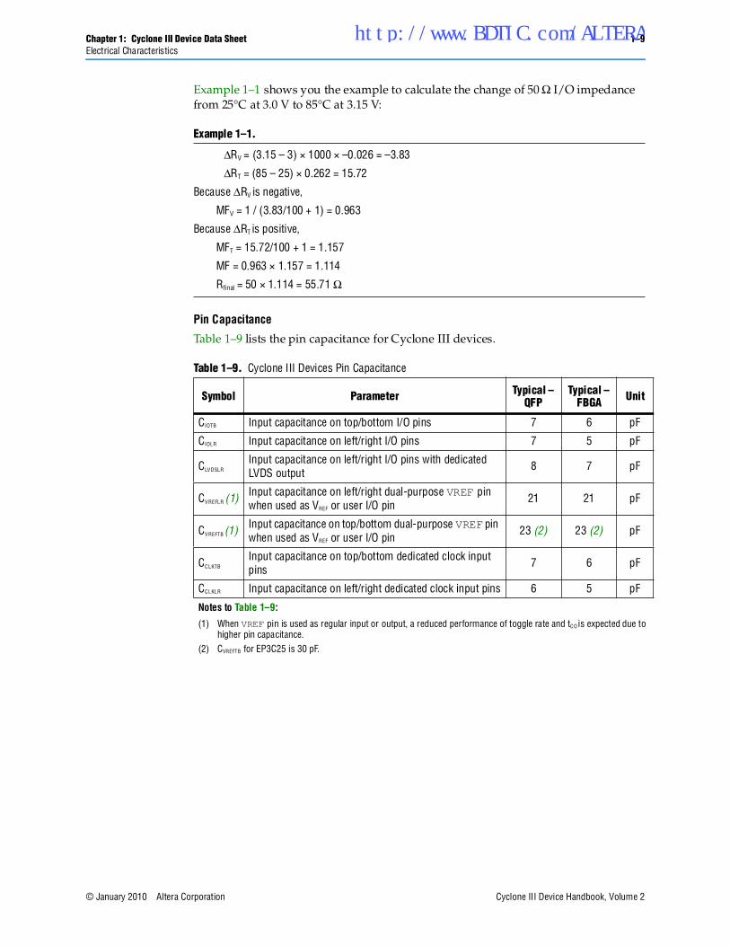
Example 1–1 shows you the example to calculate the change of 50 Ω I/O impedance from 25°C at 3.0 V to 85°C at 3.15 V:
Pin Capacitance
Table 1–9 lists the pin capacitance for Cyclone III devices.
Example 1–1.
ΔRV = (3.15 – 3) × 1000 × –0.026 = –3.83
ΔRT = (85 – 25) × 0.262 = 15.72
Because ΔRV is negative,
MFV = 1 / (3.83/100 + 1) = 0.963
Because ΔRT is positive,
MFT = 15.72/100 + 1 = 1.157
MF = 0.963 × 1.157 = 1.114
Rfinal = 50 × 1.114 = 55.71 Ω
Table 1–9. Cyclone III Devices Pin Capacitance
Symbol Parameter Typical – QFP
Typical – FBGA Unit
CIOTB Input capacitance on top/bottom I/O pins 7 6 pF
CIOLR Input capacitance on left/right I/O pins 7 5 pF
CLVDSLR
Input capacitance on left/right I/O pins with dedicated LVDS output
8 7 pF
CVREFLR (1) Input capacitance on left/right dual-purpose VREF pin when used as VREF or user I/O pin
21 21 pF
CVREFTB (1) Input capacitance on top/bottom dual-purpose VREF pin when used as VREF or user I/O pin
23 (2) 23 (2) pF
CCLKTB
Input capacitance on top/bottom dedicated clock input pins
7 6 pF
CCLKLR Input capacitance on left/right dedicated clock input pins 6 5 pF
Notes to Table 1–9:
(1) When VREF pin is used as regular input or output, a reduced performance of toggle rate and tCO is expected due to higher pin capacitance.
(2) CVREFTB for EP3C25 is 30 pF.
http://www.BDTIC.com/ALTERA
1–10 Chapter 1: Cyclone III Device Data SheetElectrical Characteristics
Cyclone III Device Handbook, Volume 2 © January 2010 Altera Corporation
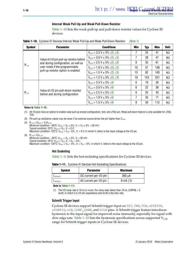
Internal Weak Pull-Up and Weak Pull-Down Resistor
Table 1–10 lists the weak pull-up and pull-down resistor values for Cyclone III devices.
Hot Socketing
Table 1–11 lists the hot-socketing specifications for Cyclone III devices.
Schmitt Trigger Input
Cyclone III devices support Schmitt trigger input on TDI, TMS, TCK, nSTATUS, nCONFIG, nCE, CONF_DONE, and DCLK pins. A Schmitt trigger feature introduces hysteresis to the input signal for improved noise immunity, especially for signal with slow edge rate. Table 1–12 lists the hysteresis specifications across supported VCCIO range for Schmitt trigger inputs in Cyclone III devices.
Table 1–10. Cyclone III Devices Internal Weak Pull-Up and Weak Pull-Down Resistor (Note 1)
Symbol Parameter Conditions Min Typ Max Unit
R_PU
Value of I/O pin pull-up resistor before and during configuration, as well as user mode if the programmable pull-up resistor option is enabled
VCCIO = 3.3 V ± 5% (2), (3) 7 25 41 kΩ
VCCIO = 3.0 V ± 5% (2), (3) 7 28 47 kΩ
VCCIO = 2.5 V ± 5% (2), (3) 8 35 61 kΩ
VCCIO = 1.8 V ± 5% (2), (3) 10 57 108 kΩ
VCCIO = 1.5 V ± 5% (2), (3) 13 82 163 kΩ
VCCIO = 1.2 V ± 5% (2), (3) 19 143 351 kΩ
R_PD
Value of I/O pin pull-down resistor before and during configuration
VCCIO = 3.3 V ± 5% (4) 6 19 30 kΩ
VCCIO = 3.0 V ± 5% (4) 6 22 36 kΩ
VCCIO = 2.5 V ± 5% (4) 6 25 43 kΩ
VCCIO = 1.8 V ± 5% (4) 7 35 71 kΩ
VCCIO = 1.5 V ± 5% (4) 8 50 112 kΩ
Notes to Table 1–10:
(1) All I/O pins have an option to enable weak pull-up except configuration, test, and JTAG pin. Weak pull-down feature is only available for JTAG TCK.
(2) Pin pull-up resistance values may be lower if an external source drives the pin higher than VCCIO.(3) R_PU = (VCCIO – VI)/IR_PU
Minimum condition: –40°C; VCCIO = VCC + 5%, VI = VCC + 5% – 50 mV;Typical condition: 25°C; VCCIO = VCC, VI = 0 V;Maximum condition: 125°C; VCCIO = VCC – 5%, VI = 0 V; in which VI refers to the input voltage at the I/O pin.
(4) R_PD = VI/IR_PD
Minimum condition: –40°C; VCCIO = VCC + 5%, VI = 50 mV;Typical condition: 25°C; VCCIO = VCC, VI = VCC – 5%;Maximum condition: 125°C; VCCIO = VCC – 5%, VI = VCC – 5%; in which VI refers to the input voltage at the I/O pin.
Table 1–11. Cyclone III Devices Hot-Socketing Specifications
Symbol Parameter Maximum
IIOPIN(DC) DC current per I/O pin 300 μA
IIOPIN(AC) AC current per I/O pin 8 mA (1)
Note to Table 1–11:
(1) The I/O ramp rate is 10 ns or more. For ramp rates faster than 10 ns, |IIOPIN| = C dv/dt, in which C is I/O pin capacitance and dv/dt is the slew rate.
http://www.BDTIC.com/ALTERA
Chapter 1: Cyclone III Device Data Sheet 1–11Electrical Characteristics
© January 2010 Altera Corporation Cyclone III Device Handbook, Volume 2
I/O Standard SpecificationsThe following tables list input voltage sensitivities (VIH and VIL), output voltage (VOH and VOL), and current drive characteristics (IOH and IOL) for various I/O standards supported by Cyclone III devices. Table 1–13 through Table 1–18 provide the I/O standard specifications for Cyclone III devices.
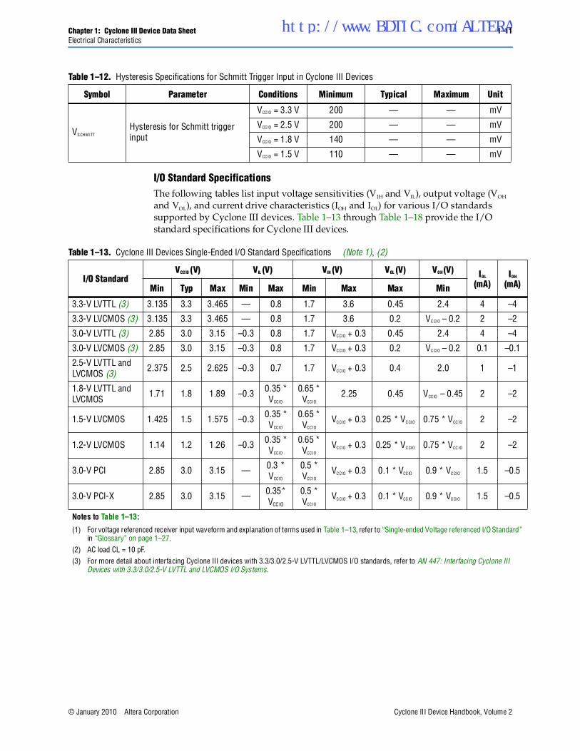
Table 1–12. Hysteresis Specifications for Schmitt Trigger Input in Cyclone III Devices
Symbol Parameter Conditions Minimum Typical Maximum Unit
VSCHMITT
Hysteresis for Schmitt trigger input
VCCIO = 3.3 V 200 — — mV
VCCIO = 2.5 V 200 — — mV
VCCIO = 1.8 V 140 — — mV
VCCIO = 1.5 V 110 — — mV
Table 1–13. Cyclone III Devices Single-Ended I/O Standard Specifications (Note 1), (2)
I/O StandardVCCIO (V) VIL (V) VIH (V) VOL (V) VOH (V) IOL
(mA) IOH
(mA) Min Typ Max Min Max Min Max Max Min
3.3-V LVTTL (3) 3.135 3.3 3.465 — 0.8 1.7 3.6 0.45 2.4 4 –4
3.3-V LVCMOS (3) 3.135 3.3 3.465 — 0.8 1.7 3.6 0.2 VCCIO – 0.2 2 –2
3.0-V LVTTL (3) 2.85 3.0 3.15 –0.3 0.8 1.7 VCCIO + 0.3 0.45 2.4 4 –4
3.0-V LVCMOS (3) 2.85 3.0 3.15 –0.3 0.8 1.7 VCCIO + 0.3 0.2 VCCIO – 0.2 0.1 –0.1
2.5-V LVTTL and LVCMOS (3)
2.375 2.5 2.625 –0.3 0.7 1.7 VCCIO + 0.3 0.4 2.0 1 –1
1.8-V LVTTL and LVCMOS
1.71 1.8 1.89 –0.3 0.35 * VCCIO
0.65 * VCCIO
2.25 0.45 VCCIO – 0.45 2 –2
1.5-V LVCMOS 1.425 1.5 1.575 –0.3 0.35 * VCCIO
0.65 * VCCIO
VCCIO + 0.3 0.25 * VCCIO 0.75 * VCCIO 2 –2
1.2-V LVCMOS 1.14 1.2 1.26 –0.3 0.35 * VCCIO
0.65 * VCCIO
VCCIO + 0.3 0.25 * VCCIO 0.75 * VCCIO 2 –2
3.0-V PCI 2.85 3.0 3.15 — 0.3 * VCCIO
0.5 * VCCIO
VCCIO + 0.3 0.1 * VCCIO 0.9 * VCCIO 1.5 –0.5
3.0-V PCI-X 2.85 3.0 3.15 — 0.35* VCCIO
0.5 * VCCIO
VCCIO + 0.3 0.1 * VCCIO 0.9 * VCCIO 1.5 –0.5
Notes to Table 1–13:
(1) For voltage referenced receiver input waveform and explanation of terms used in Table 1–13, refer to “Single-ended Voltage referenced I/O Standard” in “Glossary” on page 1–27.
(2) AC load CL = 10 pF.(3) For more detail about interfacing Cyclone III devices with 3.3/3.0/2.5-V LVTTL/LVCMOS I/O standards, refer to AN 447: Interfacing Cyclone III
Devices with 3.3/3.0/2.5-V LVTTL and LVCMOS I/O Systems.
http://www.BDTIC.com/ALTERA
1–12 Chapter 1: Cyclone III Device Data SheetElectrical Characteristics
Cyclone III Device Handbook, Volume 2 © January 2010 Altera Corporation
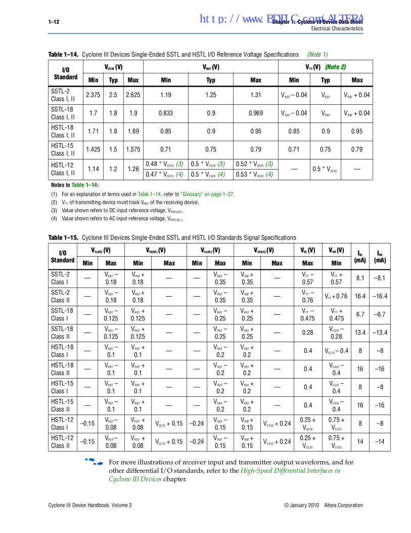
f For more illustrations of receiver input and transmitter output waveforms, and for other differential I/O standards, refer to the High-Speed Differential Interfaces in Cyclone III Devices chapter.
Table 1–14. Cyclone III Devices Single-Ended SSTL and HSTL I/O Reference Voltage Specifications (Note 1)
I/O Standard
VCCIO (V) VREF (V) VTT (V) (Note 2)
Min Typ Max Min Typ Max Min Typ Max
SSTL-2 Class I, II
2.375 2.5 2.625 1.19 1.25 1.31 VREF – 0.04 VREF VREF + 0.04
SSTL-18 Class I, II
1.7 1.8 1.9 0.833 0.9 0.969 VREF – 0.04 VREF VREF + 0.04
HSTL-18 Class I, II
1.71 1.8 1.89 0.85 0.9 0.95 0.85 0.9 0.95
HSTL-15 Class I, II
1.425 1.5 1.575 0.71 0.75 0.79 0.71 0.75 0.79
HSTL-12 Class I, II
1.14 1.2 1.260.48 * VCCIO (3) 0.5 * VCCIO (3) 0.52 * VCCIO (3)
— 0.5 * VCCIO —0.47 * VCCIO (4) 0.5 * VCCIO (4) 0.53 * VCCIO (4)
Notes to Table 1–14:
(1) For an explanation of terms used in Table 1–14, refer to “Glossary” on page 1–27. (2) VTT of transmitting device must track VREF of the receiving device.(3) Value shown refers to DC input reference voltage, VREF(DC).(4) Value shown refers to AC input reference voltage, VREF(AC).
Table 1–15. Cyclone III Devices Single-Ended SSTL and HSTL I/O Standards Signal Specifications
I/O Standard
VIL(DC) (V) VIH(DC) (V) VIL(AC) (V) VIH(AC) (V) VOL (V) VOH (V) IOL
(mA)IOH
(mA)Min Max Min Max Min Max Min Max Max Min
SSTL-2 Class I
— VREF – 0.18
VREF + 0.18
— — VREF – 0.35
VREF + 0.35
— VTT – 0.57
VTT + 0.57
8.1 –8.1
SSTL-2 Class II
— VREF – 0.18
VREF + 0.18
— — VREF – 0.35
VREF + 0.35
— VTT – 0.76
VTT + 0.76 16.4 –16.4
SSTL-18 Class I
— VREF – 0.125
VREF + 0.125
— — VREF – 0.25
VREF + 0.25
— VTT – 0.475
VTT + 0.475
6.7 –6.7
SSTL-18 Class II
— VREF – 0.125
VREF + 0.125
— — VREF – 0.25
VREF + 0.25
— 0.28 VCCIO – 0.28
13.4 –13.4
HSTL-18 Class I
— VREF – 0.1
VREF + 0.1
— — VREF – 0.2
VREF + 0.2
— 0.4 VCCIO – 0.4 8 –8
HSTL-18 Class II
— VREF – 0.1
VREF + 0.1
— — VREF – 0.2
VREF + 0.2
— 0.4 VCCIO – 0.4
16 –16
HSTL-15 Class I
— VREF – 0.1
VREF + 0.1
— — VREF – 0.2
VREF + 0.2
— 0.4 VCCIO – 0.4
8 –8
HSTL-15 Class II
— VREF – 0.1
VREF + 0.1
— — VREF – 0.2
VREF + 0.2
— 0.4 VCCIO – 0.4
16 –16
HSTL-12 Class I
–0.15 VREF – 0.08
VREF + 0.08
VCCIO + 0.15 –0.24 VREF – 0.15
VREF + 0.15
VCCIO + 0.24 0.25 × VCCIO
0.75 × VCCIO
8 –8
HSTL-12 Class II
–0.15 VREF – 0.08
VREF + 0.08
VCCIO + 0.15 –0.24 VREF – 0.15
VREF + 0.15
VCCIO + 0.24 0.25 × VCCIO
0.75 × VCCIO
14 –14
http://www.BDTIC.com/ALTERA
Chapter 1: Cyclone III Device Data Sheet 1–13Electrical Characteristics
© January 2010 Altera Corporation Cyclone III Device Handbook, Volume 2
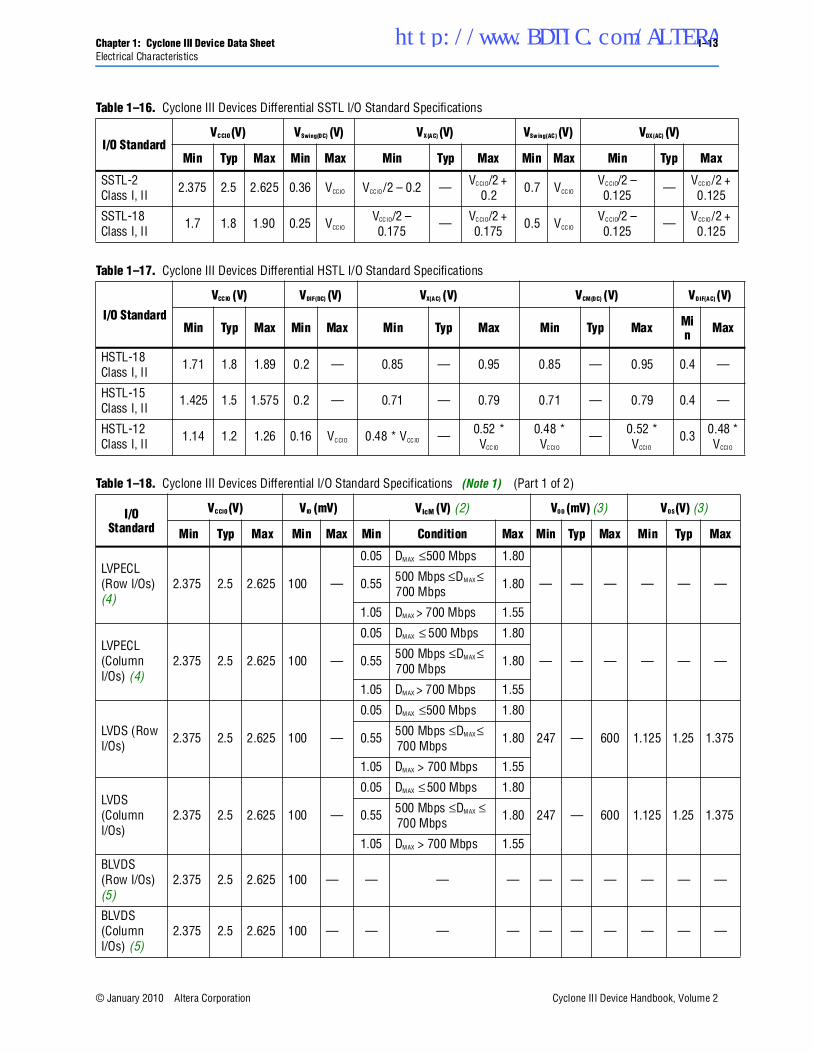
Table 1–16. Cyclone III Devices Differential SSTL I/O Standard Specifications
I/O StandardVCCIO (V) VSwing(DC) (V) VX(AC) (V) VSwing(AC) (V) VOX(AC) (V)
Min Typ Max Min Max Min Typ Max Min Max Min Typ Max
SSTL-2 Class I, II
2.375 2.5 2.625 0.36 VCCIO VCCIO/2 – 0.2 — VCCIO/2 + 0.2
0.7 VCCIO
VCCIO/2 – 0.125
— VCCIO/2 + 0.125
SSTL-18 Class I, II
1.7 1.8 1.90 0.25 VCCIO
VCCIO/2 – 0.175
— VCCIO/2 + 0.175
0.5 VCCIO
VCCIO/2 – 0.125
— VCCIO/2 + 0.125
Table 1–17. Cyclone III Devices Differential HSTL I/O Standard Specifications
I/O Standard
VCCIO (V) VDIF(DC) (V) VX(AC) (V) VCM(DC) (V) VDIF(AC) (V)
Min Typ Max Min Max Min Typ Max Min Typ Max Min Max
HSTL-18 Class I, II
1.71 1.8 1.89 0.2 — 0.85 — 0.95 0.85 — 0.95 0.4 —
HSTL-15 Class I, II
1.425 1.5 1.575 0.2 — 0.71 — 0.79 0.71 — 0.79 0.4 —
HSTL-12 Class I, II
1.14 1.2 1.26 0.16 VCCIO 0.48 * VCCIO — 0.52 * VCCIO
0.48 * VCCIO
— 0.52 * VCCIO
0.3 0.48 * VCCIO
Table 1–18. Cyclone III Devices Differential I/O Standard Specifications (Note 1) (Part 1 of 2)
I/O Standard
VCCIO (V) VID (mV) VIcM (V) (2) VOD (mV) (3) VOS (V) (3)
Min Typ Max Min Max Min Condition Max Min Typ Max Min Typ Max
LVPECL (Row I/Os) (4)
2.375 2.5 2.625 100 —
0.05 DMAX ≤ 500 Mbps 1.80
— — — — — —0.55 500 Mbps ≤ DMAX ≤ 700 Mbps
1.80
1.05 DMAX > 700 Mbps 1.55
LVPECL (Column I/Os) (4)
2.375 2.5 2.625 100 —
0.05 DMAX ≤ 500 Mbps 1.80
— — — — — —0.55 500 Mbps ≤ DMAX ≤ 700 Mbps
1.80
1.05 DMAX > 700 Mbps 1.55
LVDS (Row I/Os)
2.375 2.5 2.625 100 —
0.05 DMAX ≤ 500 Mbps 1.80
247 — 600 1.125 1.25 1.375 0.55 500 Mbps ≤ DMAX ≤ 700 Mbps
1.80
1.05 DMAX > 700 Mbps 1.55
LVDS (Column I/Os)
2.375 2.5 2.625 100 —
0.05 DMAX ≤ 500 Mbps 1.80
247 — 600 1.125 1.25 1.3750.55 500 Mbps ≤ DMAX ≤ 700 Mbps
1.80
1.05 DMAX > 700 Mbps 1.55
BLVDS (Row I/Os) (5)
2.375 2.5 2.625 100 — — — — — — — — — —
BLVDS (Column I/Os) (5)
2.375 2.5 2.625 100 — — — — — — — — — —
http://www.BDTIC.com/ALTERA
1–14 Chapter 1: Cyclone III Device Data SheetElectrical Characteristics
Cyclone III Device Handbook, Volume 2 © January 2010 Altera Corporation
Power ConsumptionYou can use the following methods to estimate power for a design:
■ the Excel-based EPE.
■ the Quartus II PowerPlay power analyzer feature.
The interactive Excel-based EPE is used prior to designing the device to get a magnitude estimate of the device power. The Quartus II PowerPlay power analyzer provides better quality estimates based on the specifics of the design after place-and-route is complete. The PowerPlay power analyzer can apply a combination of user-entered, simulation-derived, and estimated signal activities which, combined with detailed circuit models, can yield very accurate power estimates.
f For more information about power estimation tools, refer to the Early Power Estimator User Guide and the PowerPlay Power Analysis chapter in volume 3 of the Quartus II Handbook.
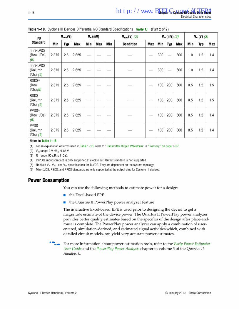
mini-LVDS (Row I/Os) (6)
2.375 2.5 2.625 — — — — — 300 — 600 1.0 1.2 1.4
mini-LVDS (Column I/Os) (6)
2.375 2.5 2.625 — — — — — 300 — 600 1.0 1.2 1.4
RSDS® (Row I/Os)(6)
2.375 2.5 2.625 — — — — — 100 200 600 0.5 1.2 1.5
RSDS (Column I/Os) (6)
2.375 2.5 2.625 — — — — — 100 200 600 0.5 1.2 1.5
PPDS®
(Row I/Os) (6)
2.375 2.5 2.625 — — — — — 100 200 600 0.5 1.2 1.4
PPDS (Column I/Os) (6)
2.375 2.5 2.625 — — — — — 100 200 600 0.5 1.2 1.4
Notes to Table 1–18:
(1) For an explanation of terms used in Table 1–18, refer to “Transmitter Output Waveform” in “Glossary” on page 1–27.(2) VIN range: 0 V ≤ VIN ≤ 1.85 V.(3) RL range: 90 ≤ RL ≤ 110 Ω.(4) LVPECL input standard is only supported at clock input. Output standard is not supported.(5) No fixed VIN , VOD , and VOS specifications for BLVDS. They are dependent on the system topology.(6) Mini-LVDS, RSDS, and PPDS standards are only supported at the output pins for Cyclone III devices.
Table 1–18. Cyclone III Devices Differential I/O Standard Specifications (Note 1) (Part 2 of 2)
I/O Standard
VCCIO (V) VID (mV) VIcM (V) (2) VOD (mV) (3) VOS (V) (3)
Min Typ Max Min Max Min Condition Max Min Typ Max Min Typ Max
http://www.BDTIC.com/ALTERA
Chapter 1: Cyclone III Device Data Sheet 1–15Switching Characteristics
© January 2010 Altera Corporation Cyclone III Device Handbook, Volume 2
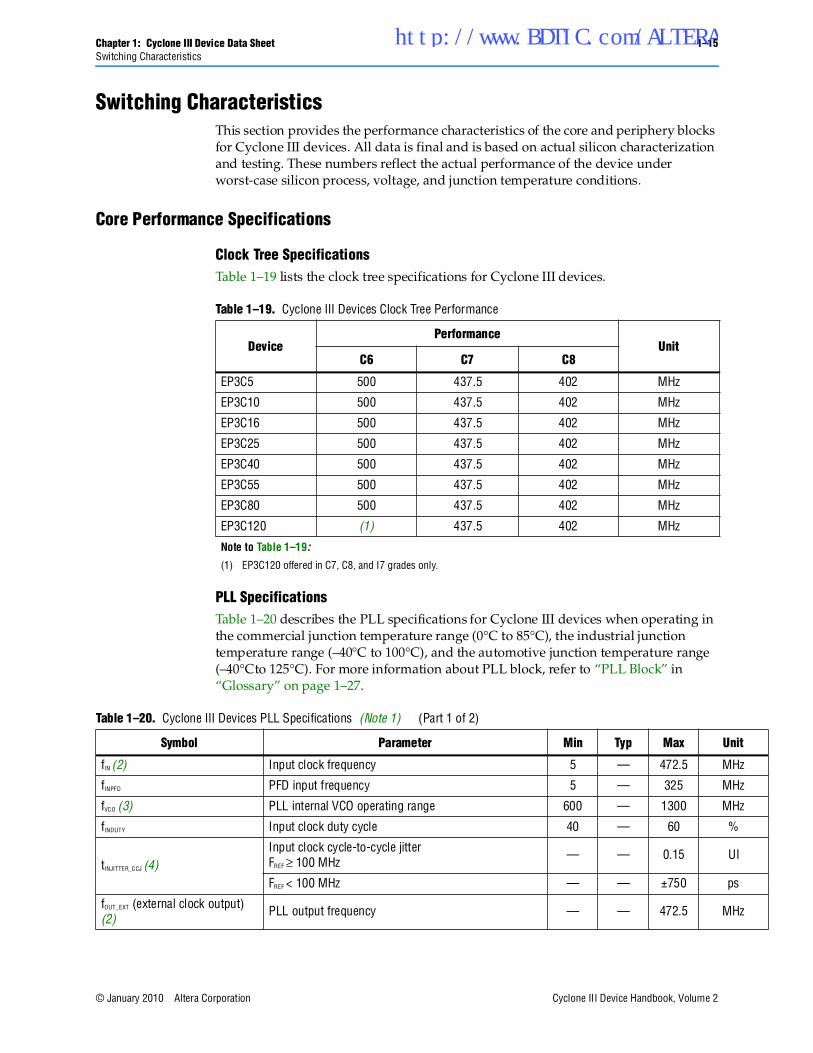
Switching CharacteristicsThis section provides the performance characteristics of the core and periphery blocks for Cyclone III devices. All data is final and is based on actual silicon characterization and testing. These numbers reflect the actual performance of the device under worst-case silicon process, voltage, and junction temperature conditions.
Core Performance Specifications
Clock Tree SpecificationsTable 1–19 lists the clock tree specifications for Cyclone III devices.
PLL SpecificationsTable 1–20 describes the PLL specifications for Cyclone III devices when operating in the commercial junction temperature range (0°C to 85°C), the industrial junction temperature range (–40°C to 100°C), and the automotive junction temperature range (–40°Cto 125°C). For more information about PLL block, refer to “PLL Block” in “Glossary” on page 1–27.
Table 1–19. Cyclone III Devices Clock Tree Performance
DevicePerformance
UnitC6 C7 C8
EP3C5 500 437.5 402 MHz
EP3C10 500 437.5 402 MHz
EP3C16 500 437.5 402 MHz
EP3C25 500 437.5 402 MHz
EP3C40 500 437.5 402 MHz
EP3C55 500 437.5 402 MHz
EP3C80 500 437.5 402 MHz
EP3C120 (1) 437.5 402 MHz
Note to Table 1–19:
(1) EP3C120 offered in C7, C8, and I7 grades only.
Table 1–20. Cyclone III Devices PLL Specifications (Note 1) (Part 1 of 2)
Symbol Parameter Min Typ Max Unit
fIN (2) Input clock frequency 5 — 472.5 MHz
fINPFD PFD input frequency 5 — 325 MHz
fVCO (3) PLL internal VCO operating range 600 — 1300 MHz
fINDUTY Input clock duty cycle 40 — 60 %
tINJITTER_CCJ (4)Input clock cycle-to-cycle jitterFREF ≥ 100 MHz
— — 0.15 UI
FREF < 100 MHz — — ±750 ps
fOUT_EXT (external clock output) (2)
PLL output frequency — — 472.5 MHz
http://www.BDTIC.com/ALTERA
1–16 Chapter 1: Cyclone III Device Data SheetSwitching Characteristics
Cyclone III Device Handbook, Volume 2 © January 2010 Altera Corporation
fOUT (to global clock)
PLL output frequency (–6 speed grade) — — 472.5 MHz
PLL output frequency (–7 speed grade) — — 450 MHz
PLL output frequency (–8 speed grade) — — 402.5 MHz
tOUTDUTY Duty cycle for external clock output (when set to 50%) 45 50 55 %
tLOCK Time required to lock from end of device configuration — — 1 ms
tDLOCK
Time required to lock dynamically (after switchover, reconfiguring any non-post-scale counters/delays or areset is deasserted)
— — 1 ms
tOUTJITTER_PERIOD_DEDCLK (5)Dedicated clock output period jitter FOUT ≥ 100 MHz
— — 300 ps
FOUT < 100 MHz — — 30 mUI
tOUTJITTER_CCJ_DEDCLK (5)Dedicated clock output cycle-to-cycle jitter FOUT ≥ 100 MHz
— — 300 ps
FOUT < 100 MHz — — 30 mUI
tOUTJITTER_PERIOD_IO (5)Regular I/O period jitterFOUT ≥ 100 MHz
— — 650 ps
FOUT < 100 MHz — — 75 mUI
tOUTJITTER_CCJ_IO (5)Regular I/O cycle-to-cycle jitterFOUT ≥ 100 MHz
— — 650 ps
FOUT < 100 MHz — — 75 mUI
tPLL_PSERR Accuracy of PLL phase shift — — ±50 ps
tARESET Minimum pulse width on areset signal. 10 — — ns
tCONFIGPLL Time required to reconfigure scan chains for PLLs — 3.5 (6) — SCANCLK cycles
fSCANCLK scanclk frequency — — 100 MHz
Notes to Table 1–20:
(1) VCCD_PLL should always be connected to VCCINT through decoupling capacitor and ferrite bead.(2) This parameter is limited in the Quartus II software by the I/O maximum frequency. The maximum I/O frequency is different for each I/O standard.(3) The VCO frequency reported by the Quartus II software in the PLL summary section of the compilation report takes into consideration the VCO post-scale
counter K value. Therefore, if the counter K has a value of 2, the frequency reported can be lower than the fVCO specification.(4) A high input jitter directly affects the PLL output jitter. To have low PLL output clock jitter, you must provide a clean clock source, which is less than 200 ps.(5) Peak-to-peak jitter with a probability level of 10–12 (14 sigma, 99.99999999974404% confidence level). The output jitter specification applies to the intrinsic
jitter of the PLL, when an input jitter of 30 ps is applied.(6) With 100 MHz scanclk frequency.
Table 1–20. Cyclone III Devices PLL Specifications (Note 1) (Part 2 of 2)
Symbol Parameter Min Typ Max Unit
http://www.BDTIC.com/ALTERA
Chapter 1: Cyclone III Device Data Sheet 1–17Switching Characteristics
© January 2010 Altera Corporation Cyclone III Device Handbook, Volume 2
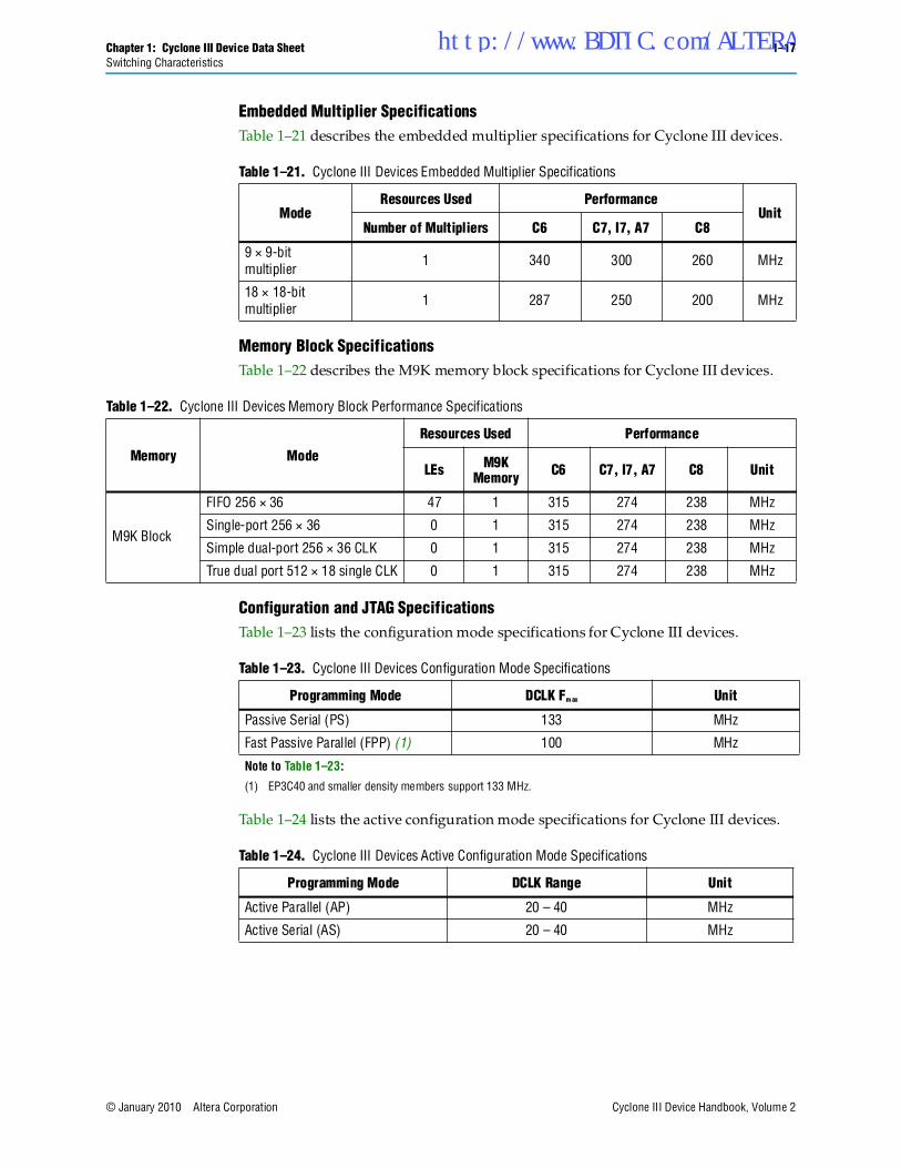
Embedded Multiplier Specifications Table 1–21 describes the embedded multiplier specifications for Cyclone III devices.
Memory Block SpecificationsTable 1–22 describes the M9K memory block specifications for Cyclone III devices.
Configuration and JTAG SpecificationsTable 1–23 lists the configuration mode specifications for Cyclone III devices.
Table 1–24 lists the active configuration mode specifications for Cyclone III devices.
Table 1–21. Cyclone III Devices Embedded Multiplier Specifications
ModeResources Used Performance
UnitNumber of Multipliers C6 C7, I7, A7 C8
9 × 9-bit multiplier
1 340 300 260 MHz
18 × 18-bit multiplier
1 287 250 200 MHz
Table 1–22. Cyclone III Devices Memory Block Performance Specifications
Memory Mode
Resources Used Performance
LEs M9K Memory C6 C7, I7, A7 C8 Unit
M9K Block
FIFO 256 × 36 47 1 315 274 238 MHz
Single-port 256 × 36 0 1 315 274 238 MHz
Simple dual-port 256 × 36 CLK 0 1 315 274 238 MHz
True dual port 512 × 18 single CLK 0 1 315 274 238 MHz
Table 1–23. Cyclone III Devices Configuration Mode Specifications
Programming Mode DCLK Fm ax Unit
Passive Serial (PS) 133 MHz
Fast Passive Parallel (FPP) (1) 100 MHz
Note to Table 1–23:
(1) EP3C40 and smaller density members support 133 MHz.
Table 1–24. Cyclone III Devices Active Configuration Mode Specifications
Programming Mode DCLK Range Unit
Active Parallel (AP) 20 – 40 MHz
Active Serial (AS) 20 – 40 MHz
http://www.BDTIC.com/ALTERA
1–18 Chapter 1: Cyclone III Device Data SheetSwitching Characteristics
Cyclone III Device Handbook, Volume 2 © January 2010 Altera Corporation
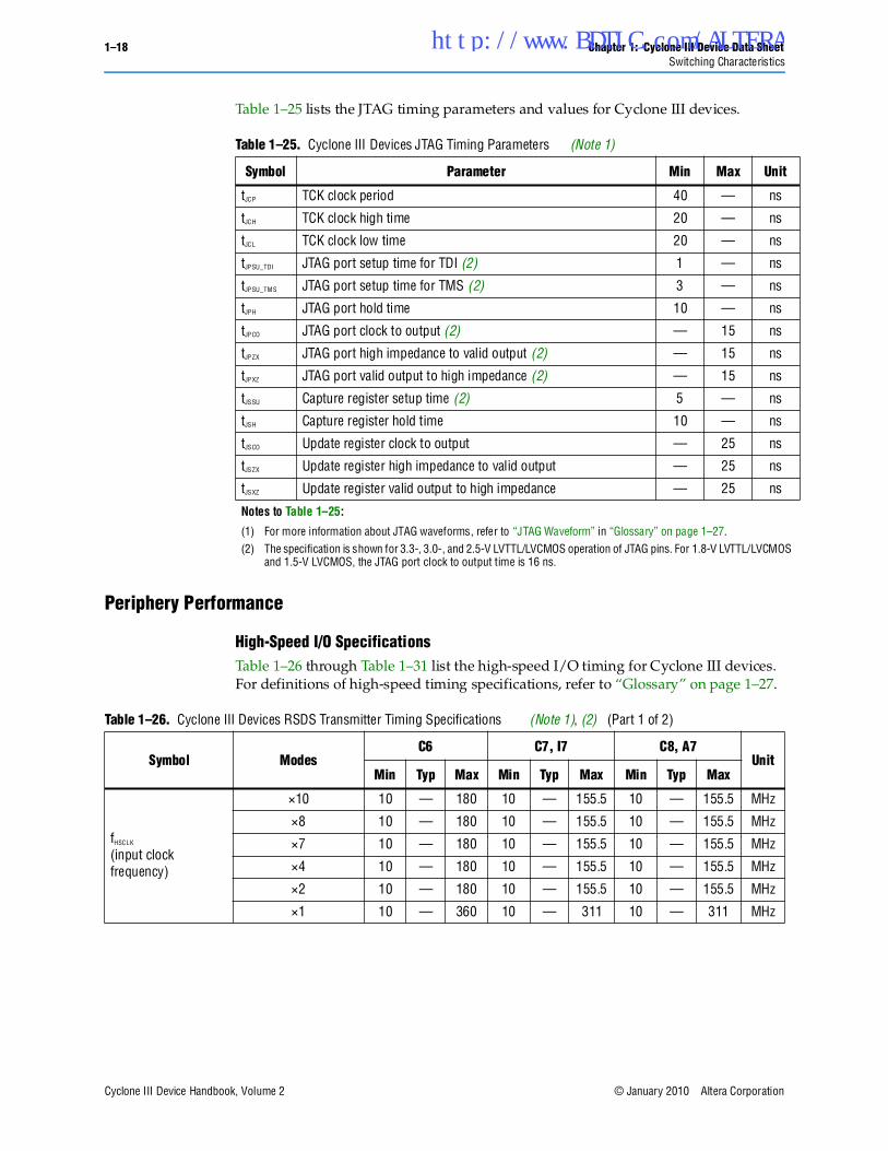
Table 1–25 lists the JTAG timing parameters and values for Cyclone III devices.
Periphery Performance
High-Speed I/O SpecificationsTable 1–26 through Table 1–31 list the high-speed I/O timing for Cyclone III devices. For definitions of high-speed timing specifications, refer to “Glossary” on page 1–27.
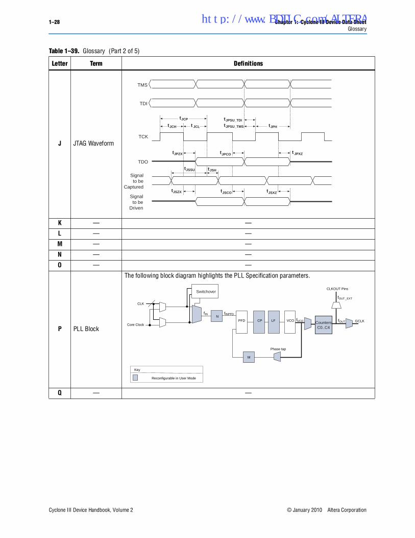
Table 1–25. Cyclone III Devices JTAG Timing Parameters (Note 1)
Symbol Parameter Min Max Unit
tJCP TCK clock period 40 — ns
tJCH TCK clock high time 20 — ns
tJCL TCK clock low time 20 — ns
tJPSU_TDI JTAG port setup time for TDI (2) 1 — ns
tJPSU_TMS JTAG port setup time for TMS (2) 3 — ns
tJPH JTAG port hold time 10 — ns
tJPCO JTAG port clock to output (2) — 15 ns
tJPZX JTAG port high impedance to valid output (2) — 15 ns
tJPXZ JTAG port valid output to high impedance (2) — 15 ns
tJSSU Capture register setup time (2) 5 — ns
tJSH Capture register hold time 10 — ns
tJSCO Update register clock to output — 25 ns
tJSZX Update register high impedance to valid output — 25 ns
tJSXZ Update register valid output to high impedance — 25 ns
Notes to Table 1–25:
(1) For more information about JTAG waveforms, refer to “JTAG Waveform” in “Glossary” on page 1–27.(2) The specification is shown for 3.3-, 3.0-, and 2.5-V LVTTL/LVCMOS operation of JTAG pins. For 1.8-V LVTTL/LVCMOS
and 1.5-V LVCMOS, the JTAG port clock to output time is 16 ns.
Table 1–26. Cyclone III Devices RSDS Transmitter Timing Specifications (Note 1), (2) (Part 1 of 2)
Symbol ModesC6 C7, I7 C8, A7
UnitMin Typ Max Min Typ Max Min Typ Max
fHSCLK
(input clock frequency)
×10 10 — 180 10 — 155.5 10 — 155.5 MHz
×8 10 — 180 10 — 155.5 10 — 155.5 MHz
×7 10 — 180 10 — 155.5 10 — 155.5 MHz
×4 10 — 180 10 — 155.5 10 — 155.5 MHz
×2 10 — 180 10 — 155.5 10 — 155.5 MHz
×1 10 — 360 10 — 311 10 — 311 MHz
http://www.BDTIC.com/ALTERA
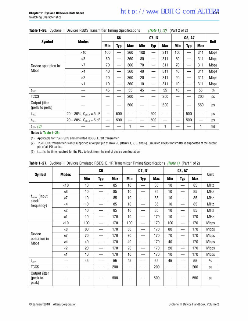
Chapter 1: Cyclone III Device Data Sheet 1–19Switching Characteristics
© January 2010 Altera Corporation Cyclone III Device Handbook, Volume 2
Device operation in Mbps
×10 100 — 360 100 — 311 100 — 311 Mbps
×8 80 — 360 80 — 311 80 — 311 Mbps
×7 70 — 360 70 — 311 70 — 311 Mbps
×4 40 — 360 40 — 311 40 — 311 Mbps
×2 20 — 360 20 — 311 20 — 311 Mbps
×1 10 — 360 10 — 311 10 — 311 Mbps
tDUTY — 45 — 55 45 — 55 45 — 55 %
TCCS — — — 200 — — 200 — — 200 ps
Output jitter(peak to peak)
— — — 500 — — 500 — — 550 ps
tRISE 20 – 80%, CLOAD = 5 pF — 500 — — 500 — — 500 — ps
tFALL 20 – 80%, CLOAD = 5 pF — 500 — — 500 — — 500 — ps
tLOCK (3) — — — 1 — — 1 — — 1 ms
Notes to Table 1–26:
(1) Applicable for true RSDS and emulated RSDS_E_3R transmitter.(2) True RSDS transmitter is only supported at output pin of Row I/O (Banks 1, 2, 5, and 6). Emulated RSDS transmitter is supported at the output
pin of all I/O banks.(3) tLOCK is the time required for the PLL to lock from the end of device configuration.
Table 1–26. Cyclone III Devices RSDS Transmitter Timing Specifications (Note 1), (2) (Part 2 of 2)
Symbol ModesC6 C7, I7 C8, A7
UnitMin Typ Max Min Typ Max Min Typ Max
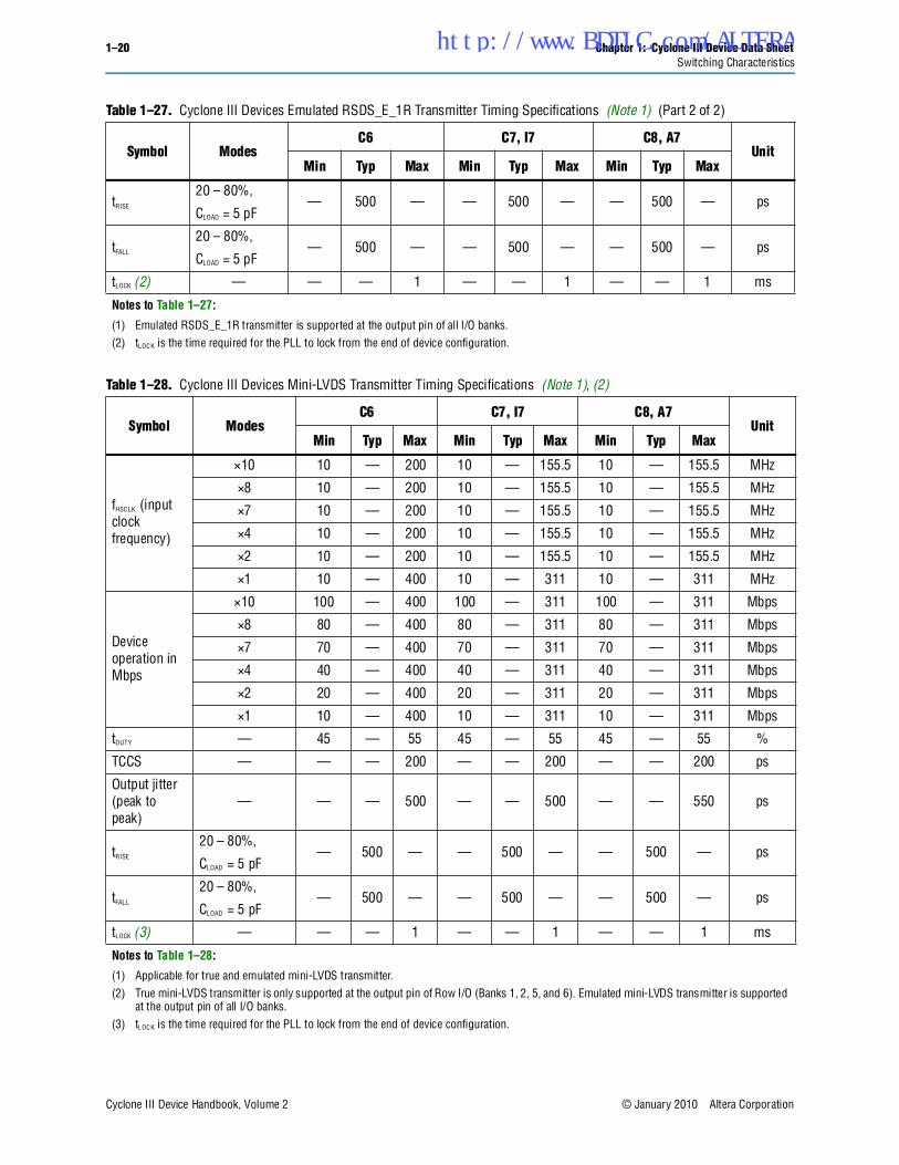
Table 1–27. Cyclone III Devices Emulated RSDS_E_1R Transmitter Timing Specifications (Note 1) (Part 1 of 2)
Symbol ModesC6 C7, I7 C8, A7
UnitMin Typ Max Min Typ Max Min Typ Max
fHSCLK (input clock frequency)
×10 10 — 85 10 — 85 10 — 85 MHz
×8 10 — 85 10 — 85 10 — 85 MHz
×7 10 — 85 10 — 85 10 — 85 MHz
×4 10 — 85 10 — 85 10 — 85 MHz
×2 10 — 85 10 — 85 10 — 85 MHz
×1 10 — 170 10 — 170 10 — 170 MHz
Device operation in Mbps
×10 100 — 170 100 — 170 100 — 170 Mbps
×8 80 — 170 80 — 170 80 — 170 Mbps
×7 70 — 170 70 — 170 70 — 170 Mbps
×4 40 — 170 40 — 170 40 — 170 Mbps
×2 20 — 170 20 — 170 20 — 170 Mbps
×1 10 — 170 10 — 170 10 — 170 Mbps
tDUTY — 45 — 55 45 — 55 45 — 55 %
TCCS — — — 200 — — 200 — — 200 ps
Output jitter(peak to peak)
— — — 500 — — 500 — — 550 ps
http://www.BDTIC.com/ALTERA
1–20 Chapter 1: Cyclone III Device Data SheetSwitching Characteristics
Cyclone III Device Handbook, Volume 2 © January 2010 Altera Corporation
tRISE
20 – 80%,
CLOAD = 5 pF— 500 — — 500 — — 500 — ps
tFALL
20 – 80%,
CLOAD = 5 pF— 500 — — 500 — — 500 — ps
tLOCK (2) — — — 1 — — 1 — — 1 ms
Notes to Table 1–27:
(1) Emulated RSDS_E_1R transmitter is supported at the output pin of all I/O banks.(2) tLOCK is the time required for the PLL to lock from the end of device configuration.
Table 1–27. Cyclone III Devices Emulated RSDS_E_1R Transmitter Timing Specifications (Note 1) (Part 2 of 2)
Symbol ModesC6 C7, I7 C8, A7
UnitMin Typ Max Min Typ Max Min Typ Max
Table 1–28. Cyclone III Devices Mini-LVDS Transmitter Timing Specifications (Note 1), (2)
Symbol ModesC6 C7, I7 C8, A7
UnitMin Typ Max Min Typ Max Min Typ Max
fHSCLK (input clock frequency)
×10 10 — 200 10 — 155.5 10 — 155.5 MHz
×8 10 — 200 10 — 155.5 10 — 155.5 MHz
×7 10 — 200 10 — 155.5 10 — 155.5 MHz
×4 10 — 200 10 — 155.5 10 — 155.5 MHz
×2 10 — 200 10 — 155.5 10 — 155.5 MHz
×1 10 — 400 10 — 311 10 — 311 MHz
Device operation in Mbps
×10 100 — 400 100 — 311 100 — 311 Mbps
×8 80 — 400 80 — 311 80 — 311 Mbps
×7 70 — 400 70 — 311 70 — 311 Mbps
×4 40 — 400 40 — 311 40 — 311 Mbps
×2 20 — 400 20 — 311 20 — 311 Mbps
×1 10 — 400 10 — 311 10 — 311 Mbps
tDUTY — 45 — 55 45 — 55 45 — 55 %
TCCS — — — 200 — — 200 — — 200 ps
Output jitter(peak to peak)
— — — 500 — — 500 — — 550 ps
tRISE
20 – 80%,
CLOAD = 5 pF— 500 — — 500 — — 500 — ps
tFALL
20 – 80%,
CLOAD = 5 pF— 500 — — 500 — — 500 — ps
tLOCK (3) — — — 1 — — 1 — — 1 ms
Notes to Table 1–28:
(1) Applicable for true and emulated mini-LVDS transmitter.(2) True mini-LVDS transmitter is only supported at the output pin of Row I/O (Banks 1, 2, 5, and 6). Emulated mini-LVDS transmitter is supported
at the output pin of all I/O banks.(3) tLOCK is the time required for the PLL to lock from the end of device configuration.
http://www.BDTIC.com/ALTERA
Chapter 1: Cyclone III Device Data Sheet 1–21Switching Characteristics
© January 2010 Altera Corporation Cyclone III Device Handbook, Volume 2
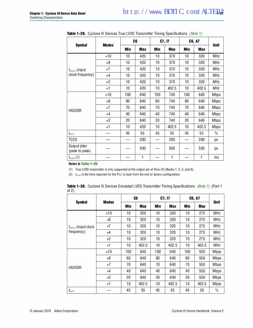
Table 1–29. Cyclone III Devices True LVDS Transmitter Timing Specifications (Note 1)
Symbol ModesC6 C7, I7 C8, A7
UnitMin Max Min Max Min Max
fHSCLK (input clock frequency)
×10 10 420 10 370 10 320 MHz
×8 10 420 10 370 10 320 MHz
×7 10 420 10 370 10 320 MHz
×4 10 420 10 370 10 320 MHz
×2 10 420 10 370 10 320 MHz
×1 10 420 10 402.5 10 402.5 MHz
HSIODR
×10 100 840 100 740 100 640 Mbps
×8 80 840 80 740 80 640 Mbps
×7 70 840 70 740 70 640 Mbps
×4 40 840 40 740 40 640 Mbps
×2 20 840 20 740 20 640 Mbps
×1 10 420 10 402.5 10 402.5 Mbps
tDUTY — 45 55 45 55 45 55 %
TCCS — — 200 — 200 — 200 ps
Output jitter(peak to peak)
— — 500 — 500 — 550 ps
tLOCK (2) — — 1 — 1 — 1 ms
Notes to Table 1–29:
(1) True LVDS transmitter is only supported at the output pin of Row I/O (Banks 1, 2, 5, and 6).(2) tLOCK is the time required for the PLL to lock from the end of device configuration.
Table 1–30. Cyclone III Devices Emulated LVDS Transmitter Timing Specifications (Note 1) (Part 1 of 2)
Symbol ModesC6 C7, I7 C8, A7
UnitMin Max Min Max Min Max
fHSCLK (input clock frequency)
×10 10 320 10 320 10 275 MHz
×8 10 320 10 320 10 275 MHz
×7 10 320 10 320 10 275 MHz
×4 10 320 10 320 10 275 MHz
×2 10 320 10 320 10 275 MHz
×1 10 402.5 10 402.5 10 402.5 MHz
HSIODR
×10 100 640 100 640 100 550 Mbps
×8 80 640 80 640 80 550 Mbps
×7 70 640 70 640 70 550 Mbps
×4 40 640 40 640 40 550 Mbps
×2 20 640 20 640 20 550 Mbps
×1 10 402.5 10 402.5 10 402.5 Mbps
tDUTY — 45 55 45 55 45 55 %
http://www.BDTIC.com/ALTERA
1–22 Chapter 1: Cyclone III Device Data SheetSwitching Characteristics
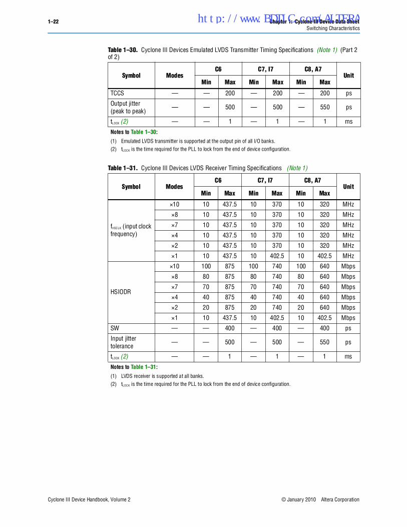
Cyclone III Device Handbook, Volume 2 © January 2010 Altera Corporation
TCCS — — 200 — 200 — 200 ps
Output jitter(peak to peak)
— — 500 — 500 — 550 ps
tLOCK (2) — — 1 — 1 — 1 ms
Notes to Table 1–30:
(1) Emulated LVDS transmitter is supported at the output pin of all I/O banks.(2) tLOCK is the time required for the PLL to lock from the end of device configuration.
Table 1–31. Cyclone III Devices LVDS Receiver Timing Specifications (Note 1)
Symbol ModesC6 C7, I7 C8, A7
UnitMin Max Min Max Min Max
fHSCLK (input clock frequency)
×10 10 437.5 10 370 10 320 MHz
×8 10 437.5 10 370 10 320 MHz
×7 10 437.5 10 370 10 320 MHz
×4 10 437.5 10 370 10 320 MHz
×2 10 437.5 10 370 10 320 MHz
×1 10 437.5 10 402.5 10 402.5 MHz
HSIODR
×10 100 875 100 740 100 640 Mbps
×8 80 875 80 740 80 640 Mbps
×7 70 875 70 740 70 640 Mbps
×4 40 875 40 740 40 640 Mbps
×2 20 875 20 740 20 640 Mbps
×1 10 437.5 10 402.5 10 402.5 Mbps
SW — — 400 — 400 — 400 ps
Input jitter tolerance
— — 500 — 500 — 550 ps
tLOCK (2) — — 1 — 1 — 1 ms
Notes to Table 1–31:
(1) LVDS receiver is supported at all banks. (2) tLOCK is the time required for the PLL to lock from the end of device configuration.
Table 1–30. Cyclone III Devices Emulated LVDS Transmitter Timing Specifications (Note 1) (Part 2 of 2)
Symbol ModesC6 C7, I7 C8, A7
UnitMin Max Min Max Min Max
http://www.BDTIC.com/ALTERA
Chapter 1: Cyclone III Device Data Sheet 1–23Switching Characteristics
© January 2010 Altera Corporation Cyclone III Device Handbook, Volume 2
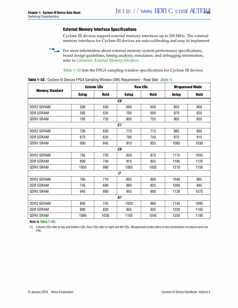
External Memory Interface Specifications Cyclone III devices support external memory interfaces up to 200 MHz. The external memory interfaces for Cyclone III devices are auto-calibrating and easy to implement.
f For more information about external memory system performance specifications, board design guidelines, timing analysis, simulation, and debugging information, refer to Literature: External Memory Interfaces.
Table 1–32 lists the FPGA sampling window specifications for Cyclone III devices.
Table 1–32. Cyclone III Devices FPGA Sampling Window (SW) Requirement – Read Side (Note 1)
Memory StandardColumn I/Os Row I/Os Wraparound Mode
Setup Hold Setup Hold Setup Hold
C6
DDR2 SDRAM 580 550 690 640 850 800
DDR SDRAM 585 535 700 650 870 820
QDRII SRAM 785 735 805 755 905 855
C7
DDR2 SDRAM 705 650 770 715 985 930
DDR SDRAM 675 620 795 740 970 915
QDRII SRAM 900 845 910 855 1085 1030
C8
DDR2 SDRAM 785 720 930 870 1115 1055
DDR SDRAM 800 740 915 855 1185 1125
QDRII SRAM 1050 990 1065 1005 1210 1150
I7
DDR2 SDRAM 765 710 855 800 1040 985
DDR SDRAM 745 690 880 825 1000 945
QDRII SRAM 945 890 955 900 1130 1075
A7
DDR2 SDRAM 805 745 1020 960 1145 1085
DDR SDRAM 880 820 955 935 1220 1160
QDRII SRAM 1090 1030 1105 1045 1250 1190
Note to Table 1–32:
(1) Column I/Os refer to top and bottom I/Os. Row I/Os refer to right and left I/Os. Wraparound mode refers to the combination of column and row I/Os.
http://www.BDTIC.com/ALTERA
1–24 Chapter 1: Cyclone III Device Data SheetSwitching Characteristics
Cyclone III Device Handbook, Volume 2 © January 2010 Altera Corporation
Table 1–33 lists the transmitter channel-to-channel skew specifications for Cyclone III devices.
Table 1–33. Cyclone III Devices Transmitter Channel-to-Channel Skew (TCCS) – Write Side (Note 1) (Part 1 of 2)
Memory Standard I/O Standard
Column I/Os (ps) Row I/Os (ps) Wraparound Mode (ps)
Lead Lag Lead Lag Lead Lag
C6
DDR2 SDRAMSSTL-18 Class I 790 380 790 380 890 480
SSTL-18 Class II 870 490 870 490 970 590
DDR SDRAMSSTL-2 Class I 750 320 750 320 850 420
SSTL-2 Class II 860 350 860 350 960 450
QDRII SRAM1.8 V HSTL Class I 780 410 780 410 880 510
1.8 V HSTL Class II 830 510 830 510 930 610
C7
DDR2 SDRAMSSTL-18 Class I 915 410 915 410 1015 510
SSTL-18 Class II 1025 545 1025 545 1125 645
DDR SDRAMSSTL-2 Class I 880 340 880 340 980 440
SSTL-2 Class II 1010 380 1010 380 1110 480
QDRII SRAM1.8 V HSTL Class I 910 450 910 450 1010 550
1.8 V HSTL Class II 1010 570 1010 570 1110 670
C8
DDR2 SDRAMSSTL-18 Class I 1040 440 1040 440 1140 540
SSTL-18 Class II 1180 600 1180 600 1280 700
DDR SDRAMSSTL-2 Class I 1010 360 1010 360 1110 460
SSTL-2 Class II 1160 410 1160 410 1260 510
QDRII SRAM1.8 V HSTL Class I 1040 490 1040 490 1140 590
1.8 V HSTL Class II 1190 630 1190 630 1290 730
I7
DDR2 SDRAMSSTL-18 Class I 961 431 961 431 1061 531
SSTL-18 Class II 1076 572 1076 572 1176 672
DDR SDRAMSSTL-2 Class I 924 357 924 357 1024 457
SSTL-2 Class II 1061 399 1061 399 1161 499
QDRII SRAM1.8 V HSTL Class I 956 473 956 473 1056 573
1.8 V HSTL Class II 1061 599 1061 599 1161 699
A7
DDR2 SDRAM (2)
SSTL-18 Class I 1092 462 1092 462 1192 562
SSTL-18 Class II 1239 630 1239 630 1339 730
DDR SDRAMSSTL-2 Class I 1061 378 1061 378 1161 478
SSTL-2 Class II 1218 431 1218 431 1318 531
http://www.BDTIC.com/ALTERA
Chapter 1: Cyclone III Device Data Sheet 1–25Switching Characteristics
© January 2010 Altera Corporation Cyclone III Device Handbook, Volume 2
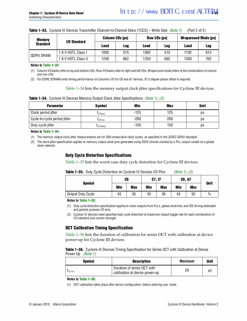
Table 1–34 lists the memory output clock jitter specifications for Cyclone III devices.
Duty Cycle Distortion SpecificationsTable 1–35 lists the worst case duty cycle distortion for Cyclone III devices.
OCT Calibration Timing SpecificationTable 1–36 lists the duration of calibration for series OCT with calibration at device power-up for Cyclone III devices.
QDRII SRAM1.8 V HSTL Class I 1092 515 1092 515 1192 615
1.8 V HSTL Class II 1250 662 1250 662 1350 762
Notes to Table 1–33:
(1) Column I/O banks refer to top and bottom I/Os. Row I/O banks refer to right and left I/Os. Wraparound mode refers to the combination of column and row I/Os.
(2) For DDR2 SDRAM write timing performance on Columns I/O for C8 and A7 devices, 97.5 degree phase offset is required.
Table 1–33. Cyclone III Devices Transmitter Channel-to-Channel Skew (TCCS) – Write Side (Note 1) (Part 2 of 2)
Memory Standard I/O Standard
Column I/Os (ps) Row I/Os (ps) Wraparound Mode (ps)
Lead Lag Lead Lag Lead Lag
Table 1–34. Cyclone III Devices Memory Output Clock Jitter Specifications (Note 1), (2)
Parameter Symbol Min Max Unit
Clock period jitter tJIT(per) -125 125 ps
Cycle-to-cycle period jitter tJIT(cc) -200 200 ps
Duty cycle jitter tJIT(duty) -150 150 ps
Notes to Table 1–34:
(1) The memory output clock jitter measurements are for 200 consecutive clock cycles, as specified in the JEDEC DDR2 standard.(2) The clock jitter specification applies to memory output clock pins generated using DDIO circuits clocked by a PLL output routed on a global
clock network.
Table 1–35. Duty Cycle Distortion on Cyclone III Devices I/O Pins (Note 1), (2)
SymbolC6 C7, I7 C8, A7
UnitMin Max Min Max Min Max
Output Duty Cycle 45 55 45 55 45 55 %
Notes to Table 1–35:
(1) Duty cycle distortion specification applies to clock outputs from PLLs, global clock tree, and IOE driving dedicated and general purpose I/O pins.
(2) Cyclone III devices meet specified duty cycle distortion at maximum output toggle rate for each combination of I/O standard and current strength.
Table 1–36. Cyclone III Devices Timing Specification for Series OCT with Calibration at Device Power-Up (Note 1)
Symbol Description Maximum Unit
tOCTCAL
Duration of series OCT with calibration at device power-up
20 µs
Notes to Table 1–36:
(1) OCT calibration takes place after device configuration, before entering user mode.
http://www.BDTIC.com/ALTERA
1–26 Chapter 1: Cyclone III Device Data SheetSwitching Characteristics
Cyclone III Device Handbook, Volume 2 © January 2010 Altera Corporation
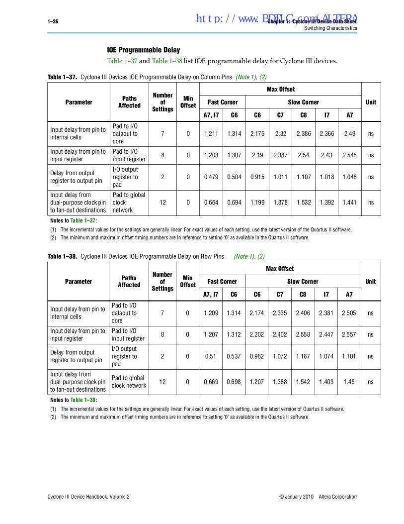
IOE Programmable DelayTable 1–37 and Table 1–38 list IOE programmable delay for Cyclone III devices.
Table 1–37. Cyclone III Devices IOE Programmable Delay on Column Pins (Note 1), (2)
Parameter Paths Affected
Number of
Settings
Min Offset
Max Offset
UnitFast Corner Slow Corner
A7, I7 C6 C6 C7 C8 I7 A7
Input delay from pin to internal cells
Pad to I/O dataout to core
7 0 1.211 1.314 2.175 2.32 2.386 2.366 2.49 ns
Input delay from pin to input register
Pad to I/O input register
8 0 1.203 1.307 2.19 2.387 2.54 2.43 2.545 ns
Delay from output register to output pin
I/O output register to pad
2 0 0.479 0.504 0.915 1.011 1.107 1.018 1.048 ns
Input delay from dual-purpose clock pin to fan-out destinations
Pad to global clock network
12 0 0.664 0.694 1.199 1.378 1.532 1.392 1.441 ns
Notes to Table 1–37:
(1) The incremental values for the settings are generally linear. For exact values of each setting, use the latest version of the Quartus II software.(2) The minimum and maximum offset timing numbers are in reference to setting ‘0’ as available in the Quartus II software.
Table 1–38. Cyclone III Devices IOE Programmable Delay on Row Pins (Note 1), (2)
Parameter Paths Affected
Number of
Settings
Min Offset
Max Offset
UnitFast Corner Slow Corner
A7, I7 C6 C6 C7 C8 I7 A7
Input delay from pin to internal cells
Pad to I/O dataout to core
7 0 1.209 1.314 2.174 2.335 2.406 2.381 2.505 ns
Input delay from pin to input register
Pad to I/O input register
8 0 1.207 1.312 2.202 2.402 2.558 2.447 2.557 ns
Delay from output register to output pin
I/O output register to pad
2 0 0.51 0.537 0.962 1.072 1.167 1.074 1.101 ns
Input delay from dual-purpose clock pin to fan-out destinations
Pad to global clock network 12 0 0.669 0.698 1.207 1.388 1.542 1.403 1.45 ns
Notes to Table 1–38:
(1) The incremental values for the settings are generally linear. For exact values of each setting, use the latest version of Quartus II software.(2) The minimum and maximum offset timing numbers are in reference to setting ‘0’ as available in the Quartus II software
http://www.BDTIC.com/ALTERA
Chapter 1: Cyclone III Device Data Sheet 1–27I/O Timing
© January 2010 Altera Corporation Cyclone III Device Handbook, Volume 2
I/O TimingYou can use the following methods to determine the I/O timing:
■ the Excel-based I/O Timing.
■ the Quartus II timing analyzer.
The Excel-based I/O Timing provides pin timing performance for each device density and speed grade. The data is typically used prior to designing the FPGA to get a timing budget estimation as part of the link timing analysis. The Quartus II timing analyzer provides a more accurate and precise I/O timing data based on the specifics of the design after place-and-route is complete.
f The Excel-based I/O Timing spreadsheet is downloadable from Cyclone III Devices Literature website.
GlossaryTable 1–39 lists the glossary for this chapter.
Table 1–39. Glossary (Part 1 of 5)
Letter Term Definitions
A — —
B — —
C — —
D — —
E — —
F fHSCLK HIGH-SPEED I/O Block: High-speed receiver/transmitter input and output clock frequency.
GGCLK Input pin directly to Global Clock network.
GCLK PLL Input pin to Global Clock network through PLL.
H HSIODR HIGH-SPEED I/O Block: Maximum/minimum LVDS data transfer rate (HSIODR = 1/TUI).
I
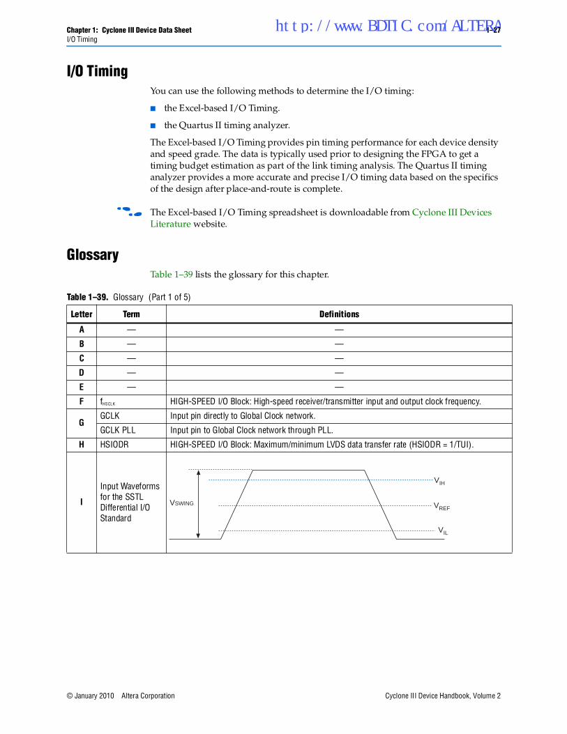
Input Waveforms for the SSTL Differential I/O Standard
VIL
VREF
VIH
VSWING
http://www.BDTIC.com/ALTERA
1–28 Chapter 1: Cyclone III Device Data SheetGlossary
Cyclone III Device Handbook, Volume 2 © January 2010 Altera Corporation
J JTAG Waveform
K — —
L — —
M — —
N — —
O — —
P PLL Block
The following block diagram highlights the PLL Specification parameters.
Q — —
Table 1–39. Glossary (Part 2 of 5)
Letter Term Definitions
TDO
TCK
tJPZX tJPCO
tJSCO tJSXZ
tJPH
tJSH
t JPXZ
tJCP
tJPSU_TMS t JCL tJCH
TDI
TMS
Signal to be
Captured
Signal to be
Driven
tJPSU_TDI
tJSZX
tJSSU
Core Clock
Phase tap
Reconfigurable in User Mode
Key
CLK
N
M
PFD VCOCP LF
CLKOUT Pins
GCLK
fINPFDfIN
fVCO fOUT
fOUT _EXT
Switchover
CountersC0..C4
http://www.BDTIC.com/ALTERA
Chapter 1: Cyclone III Device Data Sheet 1–29Glossary
© January 2010 Altera Corporation Cyclone III Device Handbook, Volume 2
R
RL Receiver differential input discrete resistor (external to Cyclone III devices).
Receiver Input Waveform
Receiver Input Waveform for LVDS and LVPECL Differential Standards.
RSKM (Receiver input skew margin)
HIGH-SPEED I/O Block: The total margin left after accounting for the sampling window and TCCS. RSKM = (TUI – SW – TCCS) / 2.
S
Single-ended Voltage referenced I/O Standard
The JEDEC standard for SSTl and HSTL I/O standards defines both the AC and DC input signal values. The AC values indicate the voltage levels at which the receiver must meet its timing specifications. The DC values indicate the voltage levels at which the final logic state of the receiver is unambiguously defined. After the receiver input crosses the AC value, the receiver changes to the new logic state. The new logic state is then maintained as long as the input stays beyond the DC threshold. This approach is intended to provide predictable receiver timing in the presence of input waveform ringing.
SW (Sampling Window)
HIGH-SPEED I/O Block: The period of time during which the data must be valid to capture it correctly. The setup and hold times determine the ideal strobe position in the sampling window.
Table 1–39. Glossary (Part 3 of 5)
Letter Term Definitions
Single-Ended Waveform
Differential Waveform (Mathematical Function of Positive & Negative Channel)
Positive Channel (p) = VIH
Negative Channel (n) = VIL
Ground
VID
VID
0 V
VCM
p - n
VID
VIH(AC)
VIH(DC)
VREFVIL(DC)
VIL(AC)
VOH
VOL
VCCIO
VSS
http://www.BDTIC.com/ALTERA
1–30 Chapter 1: Cyclone III Device Data SheetGlossary
Cyclone III Device Handbook, Volume 2 © January 2010 Altera Corporation
T
tC High-speed receiver/transmitter input and output clock period.
TCCS (Channel-to-channel-skew)
HIGH-SPEED I/O Block: The timing difference between the fastest and slowest output edges, including tCO variation and clock skew. The clock is included in the TCCS measurement.
tcin Delay from clock pad to I/O input register.
tCO Delay from clock pad to I/O output.
tcout Delay from clock pad to I/O output register.
tDUTY HIGH-SPEED I/O Block: Duty cycle on high-speed transmitter output clock.
tFALL Signal High-to-low transition time (80–20%).
tH Input register hold time.
Timing Unit Interval (TUI)
HIGH-SPEED I/O block: The timing budget allowed for skew, propagation delays, and data sampling window. (TUI = 1/(Receiver Input Clock Frequency Multiplication Factor) = tC/w).
tINJITTER Period jitter on PLL clock input.
tOUTJITTER_DEDCLK Period jitter on dedicated clock output driven by a PLL.
tOUTJITTER_IO Period jitter on general purpose I/O driven by a PLL.
tpllcin Delay from PLL inclk pad to I/O input register.
tpllcout Delay from PLL inclk pad to I/O output register.
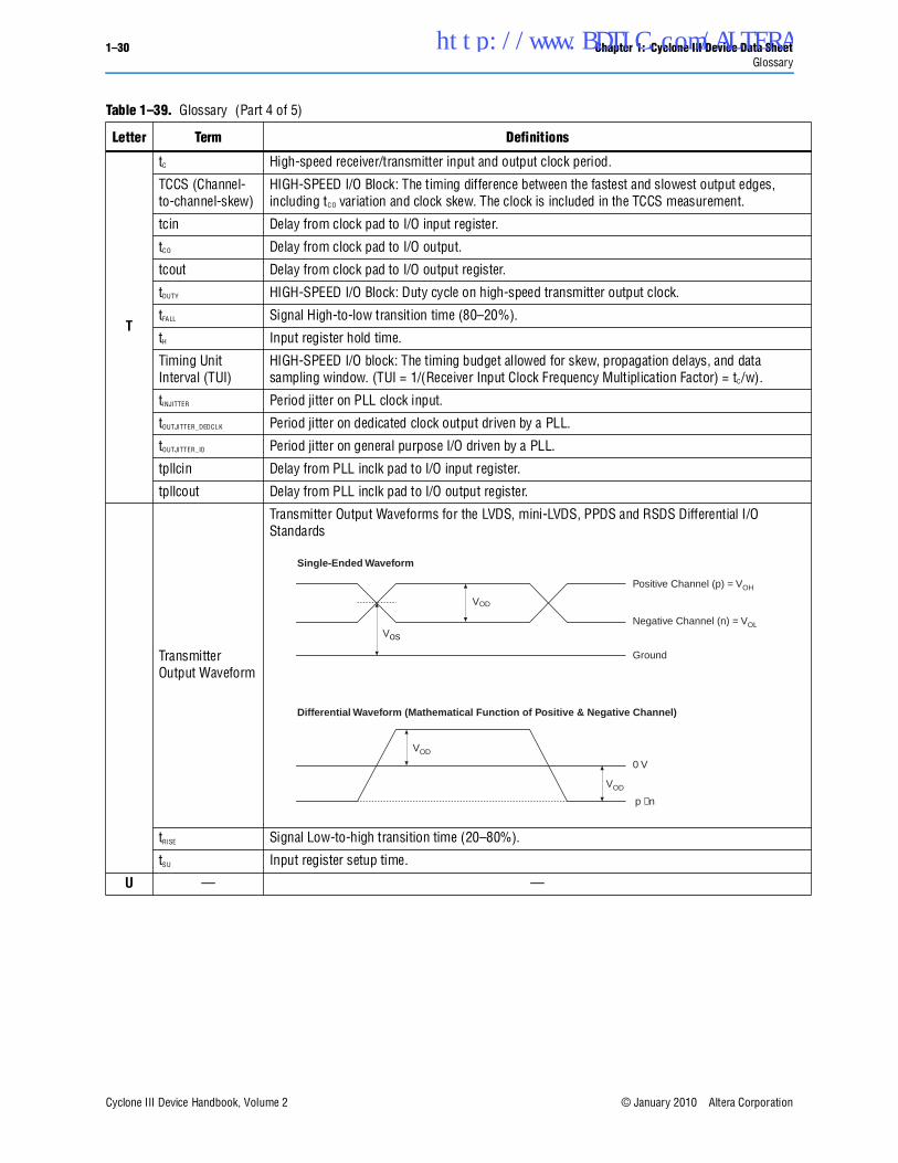
Transmitter Output Waveform
Transmitter Output Waveforms for the LVDS, mini-LVDS, PPDS and RSDS Differential I/O Standards
tRISE Signal Low-to-high transition time (20–80%).
tSU Input register setup time.
U — —
Table 1–39. Glossary (Part 4 of 5)
Letter Term Definitions
Single-Ended Waveform
Differential Waveform (Mathematical Function of Positive & Negative Channel)
Positive Channel (p) = VOH
Negative Channel (n) = VOL
Ground
VOD
VOD
VOD
0 V
Vos
p - n
http://www.BDTIC.com/ALTERA
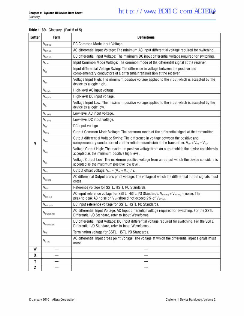
Chapter 1: Cyclone III Device Data Sheet 1–31Glossary
© January 2010 Altera Corporation Cyclone III Device Handbook, Volume 2
V
VCM(DC) DC Common Mode Input Voltage.
VDIF(AC) AC differential Input Voltage: The minimum AC input differential voltage required for switching.
VDIF(DC) DC differential Input Voltage: The minimum DC input differential voltage required for switching.
VICM Input Common Mode Voltage: The common mode of the differential signal at the receiver.
VID
Input differential Voltage Swing: The difference in voltage between the positive and complementary conductors of a differential transmission at the receiver.
VIH
Voltage Input High: The minimum positive voltage applied to the input which is accepted by the device as a logic high.
VIH(AC) High-level AC input voltage.
VIH(DC) High-level DC input voltage.
VIL
Voltage Input Low: The maximum positive voltage applied to the input which is accepted by the device as a logic low.
VIL (AC) Low-level AC input voltage.
VIL (DC) Low-level DC input voltage.
VIN DC input voltage.
VOCM Output Common Mode Voltage: The common mode of the differential signal at the transmitter.
VOD
Output differential Voltage Swing: The difference in voltage between the positive and complementary conductors of a differential transmission at the transmitter. VOD = VOH – VOL.
VOH
Voltage Output High: The maximum positive voltage from an output which the device considers is accepted as the minimum positive high level.
VOL
Voltage Output Low: The maximum positive voltage from an output which the device considers is accepted as the maximum positive low level.
VOS Output offset voltage: VOS = (VOH + VOL) / 2.
VOX (AC)
AC differential Output cross point voltage: The voltage at which the differential output signals must cross.
VREF Reference voltage for SSTL, HSTL I/O Standards.
VREF (AC)
AC input reference voltage for SSTL, HSTL I/O Standards. VREF(AC) = VREF(DC) + noise. The peak-to-peak AC noise on VREF should not exceed 2% of VREF(DC).
VREF (DC) DC input reference voltage for SSTL, HSTL I/O Standards.
VSWING (AC)
AC differential Input Voltage: AC Input differential voltage required for switching. For the SSTL Differential I/O Standard, refer to Input Waveforms.
VSWING (DC)
DC differential Input Voltage: DC Input differential voltage required for switching. For the SSTL Differential I/O Standard, refer to Input Waveforms.
VTT Termination voltage for SSTL, HSTL I/O Standards.
VX (AC)
AC differential Input cross point Voltage: The voltage at which the differential input signals must cross.
W — —
X — —
Y — —
Z — —
Table 1–39. Glossary (Part 5 of 5)
Letter Term Definitions
http://www.BDTIC.com/ALTERA
1–32 Chapter 1: Cyclone III Device Data SheetDocument Revision History
Cyclone III Device Handbook, Volume 2 © January 2010 Altera Corporation
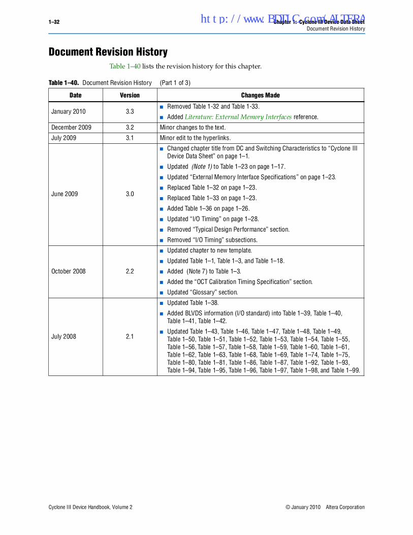
Document Revision HistoryTable 1–40 lists the revision history for this chapter.
Table 1–40. Document Revision History (Part 1 of 3)
Date Version Changes Made
January 2010 3.3■ Removed Table 1-32 and Table 1-33.
■ Added Literature: External Memory Interfaces reference.
December 2009 3.2 Minor changes to the text.
July 2009 3.1 Minor edit to the hyperlinks.
June 2009 3.0
■ Changed chapter title from DC and Switching Characteristics to “Cyclone III Device Data Sheet” on page 1–1.
■ Updated (Note 1) to Table 1–23 on page 1–17.
■ Updated “External Memory Interface Specifications” on page 1–23.
■ Replaced Table 1–32 on page 1–23.
■ Replaced Table 1–33 on page 1–23.
■ Added Table 1–36 on page 1–26.
■ Updated “I/O Timing” on page 1–28.
■ Removed “Typical Design Performance” section.
■ Removed “I/O Timing” subsections.
October 2008 2.2
■ Updated chapter to new template.
■ Updated Table 1–1, Table 1–3, and Table 1–18.
■ Added (Note 7) to Table 1–3.
■ Added the “OCT Calibration Timing Specification” section.
■ Updated “Glossary” section.
July 2008 2.1
■ Updated Table 1–38.
■ Added BLVDS information (I/O standard) into Table 1–39, Table 1–40, Table 1–41, Table 1–42.
■ Updated Table 1–43, Table 1–46, Table 1–47, Table 1–48, Table 1–49, Table 1–50, Table 1–51, Table 1–52, Table 1–53, Table 1–54, Table 1–55, Table 1–56, Table 1–57, Table 1–58, Table 1–59, Table 1–60, Table 1–61, Table 1–62, Table 1–63, Table 1–68, Table 1–69, Table 1–74, Table 1–75, Table 1–80, Table 1–81, Table 1–86, Table 1–87, Table 1–92, Table 1–93, Table 1–94, Table 1–95, Table 1–96, Table 1–97, Table 1–98, and Table 1–99.
http://www.BDTIC.com/ALTERA
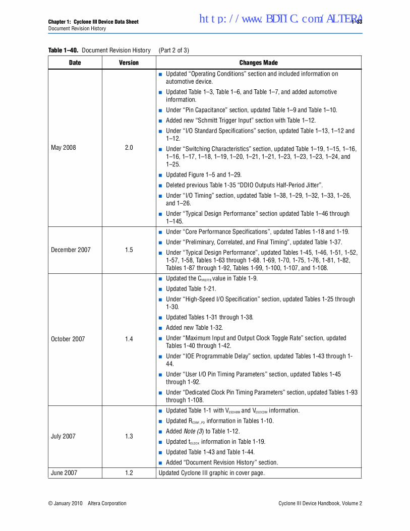
Chapter 1: Cyclone III Device Data Sheet 1–33Document Revision History
© January 2010 Altera Corporation Cyclone III Device Handbook, Volume 2
May 2008 2.0
■ Updated “Operating Conditions” section and included information on automotive device.
■ Updated Table 1–3, Table 1–6, and Table 1–7, and added automotive information.
■ Under “Pin Capacitance” section, updated Table 1–9 and Table 1–10.
■ Added new “Schmitt Trigger Input” section with Table 1–12.
■ Under “I/O Standard Specifications” section, updated Table 1–13, 1–12 and 1–12.
■ Under “Switching Characteristics” section, updated Table 1–19, 1–15, 1–16, 1–16, 1–17, 1–18, 1–19, 1–20, 1–21, 1–21, 1–23, 1–23, 1–23, 1–24, and 1–25.
■ Updated Figure 1–5 and 1–29.
■ Deleted previous Table 1-35 “DDIO Outputs Half-Period Jitter”.
■ Under “I/O Timing” section, updated Table 1–38, 1–29, 1–32, 1–33, 1–26, and 1–26.
■ Under “Typical Design Performance” section updated Table 1–46 through 1–145.
December 2007 1.5
■ Under “Core Performance Specifications”, updated Tables 1-18 and 1-19.
■ Under “Preliminary, Correlated, and Final Timing”, updated Table 1-37.
■ Under “Typical Design Performance”, updated Tables 1-45, 1-46, 1-51, 1-52, 1-57, 1-58, Tables 1-63 through 1-68. 1-69, 1-70, 1-75, 1-76, 1-81, 1-82, Tables 1-87 through 1-92, Tables 1-99, 1-100, 1-107, and 1-108.
October 2007 1.4
■ Updated the CVREFTB value in Table 1-9.
■ Updated Table 1-21.
■ Under “High-Speed I/O Specification” section, updated Tables 1-25 through 1-30.
■ Updated Tables 1-31 through 1-38.
■ Added new Table 1-32.
■ Under “Maximum Input and Output Clock Toggle Rate” section, updated Tables 1-40 through 1-42.
■ Under “IOE Programmable Delay” section, updated Tables 1-43 through 1-44.
■ Under “User I/O Pin Timing Parameters” section, updated Tables 1-45 through 1-92.
■ Under “Dedicated Clock Pin Timing Parameters” section, updated Tables 1-93 through 1-108.
July 2007 1.3
■ Updated Table 1-1 with VESDHBM and VESDCDM information.
■ Updated RCONF_PD information in Tables 1-10.
■ Added Note (3) to Table 1-12.
■ Updated tDLOCK information in Table 1-19.
■ Updated Table 1-43 and Table 1-44.
■ Added “Document Revision History” section.
June 2007 1.2 Updated Cyclone III graphic in cover page.
Table 1–40. Document Revision History (Part 2 of 3)
Date Version Changes Made
http://www.BDTIC.com/ALTERA
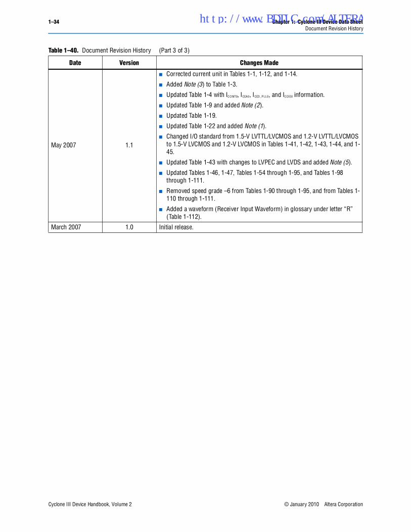
1–34 Chapter 1: Cyclone III Device Data SheetDocument Revision History
Cyclone III Device Handbook, Volume 2 © January 2010 Altera Corporation
May 2007 1.1
■ Corrected current unit in Tables 1-1, 1-12, and 1-14.
■ Added Note (3) to Table 1-3.
■ Updated Table 1-4 with ICCINT0, ICCA0, ICCD_PLL0, and ICCIO0 information.
■ Updated Table 1-9 and added Note (2).
■ Updated Table 1-19.
■ Updated Table 1-22 and added Note (1).
■ Changed I/O standard from 1.5-V LVTTL/LVCMOS and 1.2-V LVTTL/LVCMOS to 1.5-V LVCMOS and 1.2-V LVCMOS in Tables 1-41, 1-42, 1-43, 1-44, and 1-45.
■ Updated Table 1-43 with changes to LVPEC and LVDS and added Note (5).
■ Updated Tables 1-46, 1-47, Tables 1-54 through 1-95, and Tables 1-98 through 1-111.
■ Removed speed grade –6 from Tables 1-90 through 1-95, and from Tables 1-110 through 1-111.
■ Added a waveform (Receiver Input Waveform) in glossary under letter “R” (Table 1-112).
March 2007 1.0 Initial release.
Table 1–40. Document Revision History (Part 3 of 3)
Date Version Changes Made
http://www.BDTIC.com/ALTERA