
ALD deposited ferroelectric HfO2 -...
30
ALD deposited ferroelectric HfO 2 S. Slesazeck 1 , U. Schroeder 1 , E. Yurchuk 1 , J. Müller 2 , S. Müller 1 , D. Martin 1 , T. Schenk 1 , C. Richter 1 ,C. Adelmann 3 , S. Kalinin 5 , A. Kersch 7 , and T. Mikolajick 1,4 3rd ALD Symposium - SEMICON Europa October 7 th 2014 1 October 7 th , 2014 1 3 2 6 5 7
Transcript of ALD deposited ferroelectric HfO2 -...

ALD deposited ferroelectric HfO2
S. Slesazeck1, U. Schroeder1, E. Yurchuk1, J. Müller2, S. Müller1, D. Martin1, T. Schenk1,
C. Richter1,C. Adelmann3, S. Kalinin5, A. Kersch7, and T. Mikolajick1,4
3rd ALD Symposium - SEMICON Europa
October 7th 2014
1
October 7th, 2014
132 65 7

Outline
2. Stabilization of the Ferroelectric HfO2 Phase
1. Motivation: Ferroelectricity in HfO2
3. Device Application: 1T FeFET Memory
4. Summary
2S. Slesazeck et al.
SEMICON 10/2014 Grenoble

Outline
2. Stabilization of the Ferroelectric HfO2 Phase
1. Motivation: Ferroelectricity in HfO2
3. Device Application: 1T FeFET
4. Summary
3S. Slesazeck et al.
SEMICON 10/2014 Grenoble

Motivation: Ferroelectric HfO2
Ferroelectrics enablefast low power non-volatile memories
130nm FRAMp
e.g. FRAM:- current scaling limit: 130 nm
due to material properties new material necessary
TI & Ramtron
A lot of industry experienceintegrating HfO2 / ZrO2:
CMOS DRAMsub 30 nm
g g 2 2
- CMOS compatible- scalability well below 50nm- ALD process available- ferroelectric properties
chipworks
4S. Slesazeck et al.
SEMICON 10/2014 Grenoble
(IEDM 2011 / VLSI 2012 / IEDM 2013)

Motivation: 1T FeFET memory
Metal-GateF l t i
n+ n+
Ferroelectric
S b t tSemiconductor
Performanceadvantages:
• non-volatility p-Substrate
0“
non volatility• non-destructive
readoutl
noIdrain „0“
high Vth„1“
low Vth• low power
consumption• switching speed in
polarization
g pns-time range
• low operationvoltages
Vgate
voltages
5S. Slesazeck et al.
SEMICON 10/2014 Grenoble

Motivation: 1T FeFET memory
Metal-GateF l t i + +
n+ n++ + +
Ferroelectric
S b t t
-+ -+ -+Semiconductor
Performanceadvantages:
• non-volatility
0“
p-Substratenon volatility• non-destructive
readoutl Idrain „0“
high Vth• low power
consumption• switching speed in g p
ns-time range• low operation
voltages
Vgate
voltages
6S. Slesazeck et al.
SEMICON 10/2014 Grenoble

Motivation: 1T FeFET memory
Metal-GateF l t i
n+ n+- - -Ferroelectric
S b t t
-+ -+ -+Semiconductor
Performanceadvantages:
• non-volatility p-Substrate
1“
non volatility• non-destructive
readoutl Idrain „1“
low Vth• low power
consumption• switching speed in g p
ns-time range• low operation
voltages
Vgate
voltages
7S. Slesazeck et al.
SEMICON 10/2014 Grenoble

Outline
2. Stabilization of the Ferroelectric HfO2 Phase
1. Motivation: Ferroelectricity in HfO2
3. Device Application:1T FeFET
4. Summary
8S. Slesazeck et al.
SEMICON 10/2014 Grenoble

HfO2 phase stabilization
Amorphous HfO2 2
Anneal + DopingHigh-symmetry / high-k phases 4
Spinodal
1AnnealDe-mixing
+ DopingNon-centrosym. / Non-centrosym. /
Low-symmetry / lower-k phase
Non centrosym. / FE phase
Non centrosym. / ‚AFE‘ phase
lower k phase
Tetragonal P4 /nmc
Cubic Fm3m orTetragonal P42/nmc
depending on dopantOrthorhombic Pbc21 Tetragonal*
Monoclinic P21/c
16413
14Si
39Y
38
40Zr
13
14Si
9S. Slesazeck et al.
SEMICON 10/2014 Grenoble
Tetragonal/Cubic GdAlSr Al

ALD Process: doped HfO2 nanolaminates
Other precursors used for dopant supercycles:
TiN
TiPt
TiN
TiPt• tetrakis(ethylmethylamino)hafnium (TEMAHf)
• hafnium tetrachloride (HfCl4)
HfO2
TiN TiN• silicon tetrachloride (SiCl4)
• tetrakis(dimethylamino)silane (4DMAS)
TiN
SiO2• tris(dimethylamino)silane (3DMAS)
TiN
Si- wafer
Native SiO2• tris(isopropylcyclopentadienyl)gadolinium (Gd(iPrCp)3)
• tris(methylcyclopentadienyl)-yttrium (Y(MeCp)3)
• strontium di-tert-butylcyclopentadienyl (Sr(tBu3Cp)2)
• and trimethylaluminium (TMA)
O l
10S. Slesazeck et al.
SEMICON 10/2014 Grenoble
+ water, ozon or O2-plasma

Capacitor Route
Route
Anneal+ Pt Wet Etch
Layer depositi + Pt
dotsWet Etchdepositi
on
Silicon ElectrodeDeposition
HfO2deposition
Platinum dots
Simple capacitor processing
11S. Slesazeck et al.
SEMICON 10/2014 Grenoble

Effect of Si -Doping PtTiN
40
60
C/c
m2]
Electric Field [MV/cm]
Para FE AFE
TiNSi-substrate
Si:HfO2
0
20
40
lace
men
t [C
Increase of Si content
concentration
-60
-40
-20
SiO2
Elec
tric
Dis
p
0 mol % 4.4 mol % 5.6 mol % 6.6 mol % 8.5 mol %
→ Change of electrical
properties : -3 0 3 -3 0 3 -3 0 3 -3 0 3 -3 0 3E
3 5
4.0
4.5
cm2]
Effect was confirmed by
polarisation and
2.5
3.0
3.5
cita
nce
[F/
c
0 mo %
polarisation and
capacitance -voltage
measurements
1.5
2.0
-3 0 3 -3 0 3 -3 0 3 -3 0 3 -3 0 3
SiO2
Cap
ac
4,4 mol % 5,6 mol % 6,6 mol %
Electric Field [MV/cm]
8,5 mol %9 nm Si:HfO2 after 800oC AnnealPr~∫C(V)dV
12S. Slesazeck et al.
SEMICON 10/2014 Grenoble
Electric Field [MV/cm]E. Yurchuk et al., Thin Solid Films 2012
A. Toriumi at al. APL 86, 2006

Correlation to HfO2 phase
Ferroelectricity observed when th h bi h d i t
C. Richter BALD 2014
13S. Slesazeck et al.
SEMICON 10/2014 Grenoble
orthorhombic phase dominant

Different HfO2 dopants – dopant range
paraelectric
( ) ‚antiferro-electric‘ ( )
ferroelectric
0
P
paraelectric
• Ferroelectricity visible for dopands with different crystal radius
0 E
• ‚Antiferroelectricity‘ only for dopands with radius smaller than HfO2
• Dopant range larger for higher crystal radius
14S. Slesazeck et al.
SEMICON 10/2014 Grenoble
Schroeder et al., JSS 2012/JJAP 2014

Different HfO2 dopants - polarization
M i l i i i llMaximum polarization typically at
about 3-6 mol% dopant concentration
15S. Slesazeck et al.
SEMICON 10/2014 Grenoble
Schroeder et al., JJAP 2014

Outline
2. Stabilization of the Ferroelectric Phase
1. Motivation: Ferroelectricity in HfO2
3. Device Application: 1T FeFET
4. Summary
16S. Slesazeck et al.
SEMICON 10/2014 Grenoble

Ferroelectric Field Effect TransistorDevice Application: 1T FeFET
Memory Window28nm N-channel MFIS-FET
liner W
1
10
In+ n+
+ + +
- - -
-+
-+
-+
(mA
) LG : 28 nm
0 01
0.1
1 ITH
ain
curr
ent
erase100 ns
MW+5V
program100 ns-5V
20 nm
1 0 0 5 0 0 0 5 1 0 1 5
1E-3
0.01
n+ n++ ++
- - -+-
+-
+-
Dra• World‘s first 28nm FeFET
-1.0 -0.5 0.0 0.5 1.0 1.5 Gate bias (V)
World s first 28nm FeFET
• Memory window ~1V
17S. Slesazeck et al.
SEMICON 10/2014 Grenoble
E. Yurchuk et al., IEEE TED 2014

Device Application: 1T FeFETRetentionEndurance
-0.5
0.0
0.5
25 oC 85 oC 125 oCV
)Volts
)
~ 0 9V
-1.5
-1.0V TH (V
10 y
ears
0 30.60.91.2
MW
afte
r ye
ars (
V)
V t(V~ 0.9V
10-1 100 101 102 103 104 105 106 107 108
-2.0
Time (s)
1
0.00.3M 10
125 oC 85 oC 25 oC
E Yurchuk et al IEEE TED 2014
Time (s)
K Kh ll M t Th i
Memory window after 105 cycles: ~0.9VA l ti f t i h i j ti l MW
E. Yurchuk et al., IEEE TED 2014K. Khullar Master Thesis
Accumulation of asymmetric charge injection closes MW Detrap pulse can recover memory window Memory window after 10 years: ~1.0V
18S. Slesazeck et al.
SEMICON 10/2014 Grenoble
y y

Device Application: 1T FeFETFerroelectric FET Ferroelectric MIM CapEndurance
~ 0 9V~ 0.9V
C li i it li it d b b kd
K. Yurchuk PhD ThesisK. Khullar Master Thesis
• Cycling in capacitor limited by breakdown
• Cycling in transistor limited by charge trapping
19S. Slesazeck et al.
SEMICON 10/2014 Grenoble
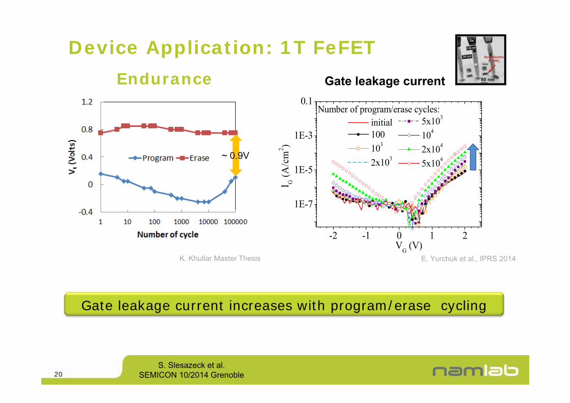
EnduranceDevice Application: 1T FeFETFerroelectric FET Gate leakage current
0.1Number of program/erase cycles:
Endurance
1E-3
Number of program/erase cycles: 5x10³ 104 2x10⁴
initial 100 103
m2 )
~ 0 9V
1E 7
1E-5 5x10⁴ 2x10³
I G (A
/cm~ 0.9V
-2 -1 0 1 2
1E-7
V (V)E. Yurchuk et al., IPRS 2014
VG (V)K. Khullar Master Thesis
Gate leakage current increases with program/erase cycling
20S. Slesazeck et al.
SEMICON 10/2014 Grenoble

Device Application: 1T FeFETI t f i l t
10 x 1011
m2 )
Variable base level charge pumpingInterfacial traps
200
250
100 101 102 103 1040
5
m2 )
x 10
Number of cycles
NC
P
(Tra
ps/c
m
100
150
after 2x10³ cycles after 103 cycles
after 5x10³ cycles I C
P (mA
/cm Number of cycles
-2 -1 0 10
50after 10 cycles
initial
2 1 0 1VGB (V)
Generation of interface traps is the root cause of degradation
E. Yurchuk et al., IPRS 2014
Generation of interface traps is the root cause of degradation
Interplay between SiO2-interface and ferroelectric HfO has to
be optimized
21S. Slesazeck et al.
SEMICON 10/2014 Grenoble
p

DRAM like FeFET:
CH Cheng et al. IEEE EDL 35, 1, 2014
- 30nm ZrHfO in FeFET: +/- 4V switching Switching in sub-cyclesS 12
Changed operation conditions can significantly improve cycling
- Switching time: 5ns 1012 endurance, but low retention: ~10s
22S. Slesazeck et al.
SEMICON 10/2014 Grenoble

Comparison NOR Flash vs. AND FeFET
NOR Flash AND FeFET DRAM DRAM
F FETspec FeFET
Write/Erase Speed 1μs/2ms 10 ns/10ns ns 5ns
Read Speed 10μs 20ns ns ?
Retention 10 yrs 10 yrs >64ms 10s
Endurance 105 cycles 104 cycles >1015 >1012Endurance y 10 cycles >10 >10
Write/Erase Voltage 10-20V 5V 0.5V 4V
FeFET meets some FLASH and DRAM specifications
23S. Slesazeck et al.
SEMICON 10/2014 Grenoble

Scaling of FeFET – grain and domain size
Grain size~30nm
TEM
Domains and grains
Domain size~300nm
and grainsbeforedevice
structuring
Domains and grainsunderneath
250 d i
Domains and grainsunderneath
25 d iPFM 250nm device 25nm device
S l l k l bl b d b h k d
PFM
- Scaling likely possible, but needs to be checked
- low variability of switching characteristics on smallest devices
24S. Slesazeck et al.
SEMICON 10/2014 Grenoble

Piezo Force Microscopy
DielectricsPiezoelectrics
PyroelectricsFerroelectrics
Ref.: http://en.wikipedia.org/wiki/Piezoresponse_Force_Microscopy
- Phase: Polarization direction detectable- Local distribution
D Martin @ Oak Ridge Nat Labs
25S. Slesazeck et al.
SEMICON 10/2014 Grenoble
D. Martin @ Oak Ridge Nat. Labs

Piezo Force Measurements
180°3
+4.2 V0°
a.u.nm3nm
2
-4.2 V0°
1
Topography Piezo responce Phase
-180°0
- Most HfO2 grains switchable
polarization value visible two polarization direction
D. Martin et al., Ad M tMost HfO2 grains switchable
- PFM serves as base for optimization of film composition
and crystallization on simple capacitor structures
Adv. Mat.submitted
U. Schroeder et al., IWDTF 2013/ JJAP 2014
26S. Slesazeck et al.
SEMICON 10/2014 Grenoble
and crystallization on simple capacitor structures JJAP 2014

Outline
2. Stabilization of the Ferroelectric HfO2 Phase
1. Motivation: Ferroelectricity in HfO2
3. Ferroelectric Switching Behavior
5. Summary
4. Device Application: 1T FeFET
27S. Slesazeck et al.
SEMICON 10/2014 Grenoble

Summary
Material:
A ferroelectric phase in HfO2 thin films can be stabilizedp 2
Ferroelectric phase most likely orthorhombic phase
Several stabilizing dopants have been identified
Ferroelectric Devices:
1T/1C: FE-HfO2 adds the 3rd dimension to FRAM scaling1T/1C: FE HfO2 adds the 3rd dimension to FRAM scaling
World‘s first 28nm FeFET device
HfO2-based FeFET added to ITRS roadmap in 2014:
Most promising ‚Emerging Memory‘ concept
FeFET meets already some DRAM and FLASH specification
Superior control of dopant concentration in ALD nanolaminates
and usbsequent crystallization of the film is mandatory
28S. Slesazeck et al.
SEMICON 10/2014 Grenoble

Thank you for your attention
This work was supported in part by the EFRE fund of the European Commission within the scope of technology development and in part by the Free State of Saxony
(Project: Cool Memory, Heiko, Merlin)
and by funding of the Deutsche Forschungs Gemeinschaft(DFG) (Project: Inferox)
29S. Slesazeck et al.
SEMICON 10/2014 Grenoble
( j )

Thanks to the FeFET – TEAM:
2 3 4
5 6 7 8 9
dand many more:
U. Schröder1, E. Yurchuk1, J. Mueller2, S. Mueller1, T. Mikolajick1
T. Boescke4, D. Martin1, D. Zhou1, J. Sundqvist2, P. Polakowski2, T. Schenk1, U. Boettger5, D. Braeuhaus5, S. Starschich5, C. Adelmann6, M.
Popovici6, T. Schloesser3, M. Trentzsch3 , M. Goldbach3, R.v. Bentum3, S. p , , , , ,Knebel1, T. Olsen1, R. Hoffmann2, J. Paul2, R. Boschke3, A. Kumar7, T.M.
Arruda7, S.V. Kalinin7, M. Alexe8, A. Morelli8, A.Kersch9, R. Maverick9
30S. Slesazeck et al.
SEMICON 10/2014 Grenoble1


![Sangeetha [Ferroelectric Memory]](https://static.fdocuments.net/doc/165x107/55cf8f91550346703b9d9665/sangeetha-ferroelectric-memory.jpg)

![FERROELECTRIC RAM [FRAM]](https://static.fdocuments.net/doc/165x107/56816799550346895ddcd567/ferroelectric-ram-fram.jpg)


