Negative Capacitance beyond Ferroelectric Switches
27
This is a repository copy of Negative Capacitance beyond Ferroelectric Switches. White Rose Research Online URL for this paper: http://eprints.whiterose.ac.uk/131637/ Version: Accepted Version Article: Kumar, A. orcid.org/0000-0002-8288-6401, Pillai, P.B., Song, X. et al. (1 more author) (2018) Negative Capacitance beyond Ferroelectric Switches. ACS Applied Materials and Interfaces, 10 (23). pp. 19812-19819. ISSN 1944-8244 https://doi.org/10.1021/acsami.8b05093 This document is the Accepted Manuscript version of a Published Work that appeared in final form in ACS Applied Materials and Interfaces, copyright © American Chemical Society after peer review and technical editing by the publisher. To access the final edited and published work see https://doi.org/10.1021/acsami.8b05093. [email protected] https://eprints.whiterose.ac.uk/ Reuse Items deposited in White Rose Research Online are protected by copyright, with all rights reserved unless indicated otherwise. They may be downloaded and/or printed for private study, or other acts as permitted by national copyright laws. The publisher or other rights holders may allow further reproduction and re-use of the full text version. This is indicated by the licence information on the White Rose Research Online record for the item. Takedown If you consider content in White Rose Research Online to be in breach of UK law, please notify us by emailing [email protected] including the URL of the record and the reason for the withdrawal request.
Transcript of Negative Capacitance beyond Ferroelectric Switches

This is a repository copy of Negative Capacitance beyond Ferroelectric Switches.
White Rose Research Online URL for this paper:http://eprints.whiterose.ac.uk/131637/
Version: Accepted Version
Article:
Kumar, A. orcid.org/0000-0002-8288-6401, Pillai, P.B., Song, X. et al. (1 more author) (2018) Negative Capacitance beyond Ferroelectric Switches. ACS Applied Materials and Interfaces, 10 (23). pp. 19812-19819. ISSN 1944-8244
https://doi.org/10.1021/acsami.8b05093
This document is the Accepted Manuscript version of a Published Work that appeared in final form in ACS Applied Materials and Interfaces, copyright © American Chemical Societyafter peer review and technical editing by the publisher. To access the final edited and published work see https://doi.org/10.1021/acsami.8b05093.
[email protected]://eprints.whiterose.ac.uk/
Reuse
Items deposited in White Rose Research Online are protected by copyright, with all rights reserved unless indicated otherwise. They may be downloaded and/or printed for private study, or other acts as permitted by national copyright laws. The publisher or other rights holders may allow further reproduction and re-use of the full text version. This is indicated by the licence information on the White Rose Research Online record for the item.
Takedown
If you consider content in White Rose Research Online to be in breach of UK law, please notify us by emailing [email protected] including the URL of the record and the reason for the withdrawal request.

1
Negative Capacitance beyond ferroelectric switches
Ashwani Kumar, Premlal Balakrishna Pillai, Xiaoyao Song, and Maria Merlyne De Souza*
Department of Electronic and Electrical Engineering, University of Sheffield−North Campus, S3
7HQ Sheffield, United Kingdom
KEYWORDS: Negative Capacitance, subthreshold slope, solid electrolyte, ferroelectric, field
effect transistors, Tantalum oxide, zinc oxide.
ABSTRACT: Negative capacitance transistors are a unique class of switches capable of operation
beyond the Boltzmann limit to realise sub-thermionic switching. Until now, the negative
capacitance effect has been predominantly attributed to devices employing an unstable insulator
with ferroelectric properties, exhibiting a two-well energy landscape, in accordance with Landau
theory. The theory and operation of a solid electrolyte Field Effect Transistor (SE-FET) of
subthreshold swing less than 60 𝑚𝑉/𝑑𝑒𝑐 in the absence of a ferroelectric gate dielectric is
demonstrated in this work. Unlike ferroelectric FETs that rely on a sudden switching of dipoles to
achieve negative capacitance, we demonstrate a distinctive mechanism that relies on the
accumulation and dispersion of ions at the interfaces of the oxide, leading to a subthreshold slope
(SS) as low as 26 𝑚𝑉/𝑑𝑒𝑐 in these samples. The frequency of operation of these unscaled devices
lies in a few milli-Hertz, because at higher or lower frequencies, the ions in the insulator are either
too fast or too slow to produce voltage amplification. This is unlike Landau switches, where the

2
SS remains below 60𝑚𝑉/𝑑𝑒𝑐 even under quasi-static sweep of the gate bias. The proposed FETs
show a higher on-current with thicker oxide in the entire range of gate voltage, clearly
distinguishing their scaling laws from those of ferroelectric FETs. Our theory validated with
experiment, demonstrates a new class of devices capable of negative capacitance that opens up
alternate methods of steep switching beyond the traditional approach of Ferroelectric or
memristive FETs.
INTRODUCTION
Complementary Metal Oxide Semiconductor (CMOS) technology is the main driver of the
contemporary information age. Its pervasiveness has been delivered by an exponential increase in
processing power of a chip via a continuous reduction in the physical dimensions of transistors by
almost a factor of half, every 18 months, according to Moore’s law. Despite continuous
downscaling, a proportional reduction in the supply voltage has been a greater challenge since the
last decade, resulting in higher density chips with increased power consumption today. This
limitation arises because the drain to source current, 𝐼𝐷𝑆, that is proportional to the gate induced
carrier density 𝑁, is exponentially dependent on the semiconductor surface potential (Ψ𝑠)1, i.e., 𝐼𝐷𝑆 ∝ 𝑁 ∝ 𝑒𝑥𝑝 (𝑞Ψ𝑠 𝑘𝐵𝑇⁄ ), requiring Ψ𝑠 to change by at least ~60 𝑚𝑉 for an order of magnitude
(a decade) change in 𝐼𝐷𝑆. Overcoming this Boltzmann limit of 2.3 𝑘𝐵𝑇 𝑞⁄ ≈ 60 𝑚𝑉/𝑑𝑒𝑐 (where 𝑘𝐵 is the Boltzmann constant, 𝑇, the temperature and 𝑞 the elementary charge) of the sub-threshold
swing (SS) of a Metal–Oxide–Semiconductor Field Effect Transistor (MOSFET) is considered as
a possible evolution of CMOS scaling below a channel length of 8 𝑛𝑚 for future logic devices2–4.
Broadly speaking, beyond the relationship between Ψ𝑠 and 𝐼𝐷𝑆 as indicated above, the SS is
affected by how well the gate can be coupled to the semiconductor, via the body factor 𝑚, where

3
𝑉𝐺𝑆 is the applied potential at the gate, distributed across the gate dielectric and the semiconductor
region of a typical transistor as
𝑉𝐺𝑆 = 𝜙𝑚𝑠 + 𝑉𝑜𝑥 + Ψ𝑠 (1)
Where 𝜙𝑚𝑠 represents the difference in work function between the gate and semiconductor, and 𝑉𝑜𝑥 is the potential drop across the dielectric. In such a case, for a constant 𝜙𝑚𝑠, 𝑚, the body factor
can be expressed as 𝑚 = 𝑑𝑉𝐺𝑆/𝑑Ψ𝑠. If the capacitances associated with the gate dielectric and the
semiconductor are represented as 𝐶𝑖𝑛𝑠 and 𝐶𝑠𝑐 respectively, the body factor 𝑚 is equal to 1 +𝐶𝑠𝑐/𝐶𝑖𝑛𝑠 > 1, giving rise to a subthreshold swing2, 𝑆𝑆 = 𝑚 × 2.3𝑘𝐵𝑇 𝑞⁄ = 𝑚 × 𝑛 > 60 𝑚𝑉/𝑑𝑒𝑐 in conventional transistors. A change in the surface potential (𝑑Ψ𝑠) larger than the change in
the applied gate bias (𝑑𝑉𝐺𝑆) is required to achieve 𝑚 < 1.
A number of alternative approaches, broadly considered subsets of “Steep Subthreshold
devices”, are now being contemplated to achieved 𝑚 < 1. Techniques that result in 𝑚 < 1, also
largely referred to as Landau switches5, are of great significance to technology, as they result in
low operating voltages and thereby reduced power consumption of electronic circuits. Amongst
such techniques, reported to date, the most promising for future technology nodes are ferroelectric
FETs (FE-FETs)6,7, initiated by the pioneering work of Salahuddin and Datta in 20088, though
others, such as piezoelectric FETs9,10, nanoelectro-mechanical FETs (NEMFETs)11–13, and phase-
FETs14,15, employing a resistive switch have also been reported. There are two important
distinctions in approach amongst the various mechanisms that are described. In one case, the net
capacitance between the gate and the semiconductor channel is boosted by introducing a material
in the gate dielectric stack with an inherent instability, such as in a FE-FETs or a NEMFET5,
depicted in Figure 1 (a). In these FETs, the energy profile of the gate dielectric stack exhibits a
dual energy-well that upon transition from one well to the other, leads to a negative capacitance
4
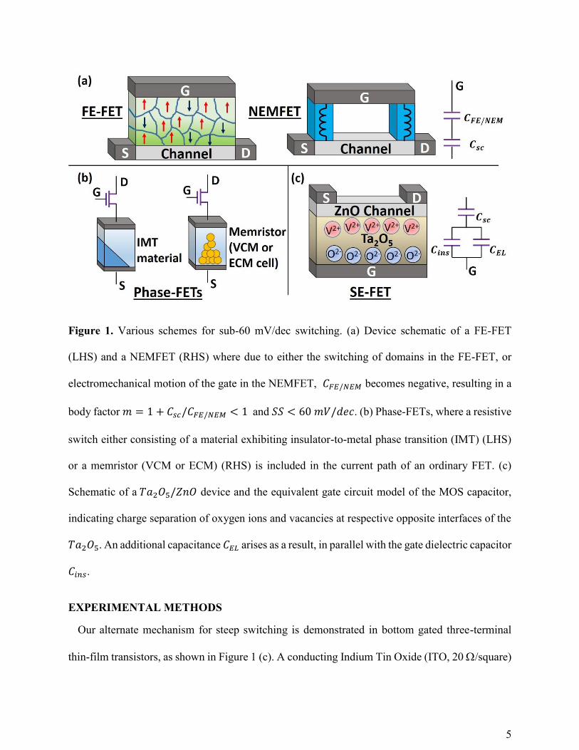
𝐶𝐹𝐸/𝑁𝐸𝑀. In the second case, the abrupt switching of a resistive switch in series with the current
flow path, between a low resistance state (LRS) and a high resistance state (HRS), is utilised to
produce steep switching. The resistive switch is typically realised either with a material exhibiting
insulator-to-metal transition (IMT) such as vanadium dioxide14 or a memristor element, as in
Figure 1 (b), realised either via a phase change memory (PCM), electrochemical metallization
memory (ECM), or valence change memory (VCM)16. In PCMs, a change in the phase of a
material, e.g. GeTe or Sb2Te3, from the amorphous to crystalline or vice-versa ‘sets’ or ‘resets’ the
device in the LRS or HRS. The ECM consists of an active electrode of Ag or Cu and a counter
electrode of e.g. Pt separated by an insulating layer of solid electrolyte, e.g. SiO2 or Ta2O5, where
resistive switching from the HRS to the LRS takes place via migration of metallic ions from the
active electrodes into the insulator, thus forming a conducting filament.17 In the case of a VCM,
the movement of negatively charged oxygen ions or positively charged vacancies in the thin film
(~10 𝑛𝑚) of, for example TaOx, HfOx, or TiOx, results in the formation/dissolution of a vacancy
rich conducting filament that is responsible for resistive switching.18
In this work, we demonstrate an alternate Negative Capacitance mechanism to achieve steep
switching characteristics but only under dynamic operation in 𝑇𝑎2𝑂5/𝑍𝑛𝑂 solid electrolyte (SE-)
FETs, shown in Figure 1 (c). As indicated in this figure, the presence of doubly charged mobile
oxygen ions and vacancies in the 𝑇𝑎2𝑂5, induces a sheet charge at the interface of 𝑇𝑎2𝑂5 and 𝑍𝑛𝑂, which gives rise to an additional electrolytic capacitance, indicated by 𝐶𝐸𝐿 in the equivalent
circuit diagram. We develop a theoretical framework that provides evidence that under a dynamic
sweep of the gate bias, 𝐶𝐸𝐿 achieves a negative value such that |𝐶𝐸𝐿| > 𝐶𝑖𝑛𝑠, leading to sub-60 𝑚𝑉/𝑑𝑒𝑐 switching, yet without the involvement of any ferroelectric material or filamentary
processes in the gate insulator.
5
Figure 1. Various schemes for sub-60 mV/dec switching. (a) Device schematic of a FE-FET
(LHS) and a NEMFET (RHS) where due to either the switching of domains in the FE-FET, or
electromechanical motion of the gate in the NEMFET, 𝐶𝐹𝐸/𝑁𝐸𝑀 becomes negative, resulting in a
body factor 𝑚 = 1 + 𝐶𝑠𝑐/𝐶𝐹𝐸/𝑁𝐸𝑀 < 1 and 𝑆𝑆 < 60 𝑚𝑉/𝑑𝑒𝑐. (b) Phase-FETs, where a resistive
switch either consisting of a material exhibiting insulator-to-metal phase transition (IMT) (LHS)
or a memristor (VCM or ECM) (RHS) is included in the current path of an ordinary FET. (c)
Schematic of a 𝑇𝑎2𝑂5/𝑍𝑛𝑂 device and the equivalent gate circuit model of the MOS capacitor,
indicating charge separation of oxygen ions and vacancies at respective opposite interfaces of the 𝑇𝑎2𝑂5. An additional capacitance 𝐶𝐸𝐿 arises as a result, in parallel with the gate dielectric capacitor 𝐶𝑖𝑛𝑠.
EXPERIMENTAL METHODS
Our alternate mechanism for steep switching is demonstrated in bottom gated three-terminal
thin-film transistors, as shown in Figure 1 (c). A conducting Indium Tin Oxide (ITO, 20 /square)

6
is used as gate, thicknesses of 120 and 275 𝑛𝑚 of tantalum oxide (𝑇𝑎2𝑂5) of dielectric constant 𝜖𝑇𝑎2𝑂5 ≈ 20.8 are deposited as the gate insulator and 40 𝑛𝑚 of zinc oxide as channel, via RF
sputtering as reported in ref 19. The sputtered 𝑇𝑎2𝑂5 results in an amorphous phase, as the
temperature required for crystallisation is more than 1000 K20. All the measurements of electrical
characteristics are carried out using an Agilent B1500.
RESULTS AND DISCUSSION
The drain current characteristics are examined in the forward and backward directions at scan
rates of gate voltage ranging from 2.17 𝑚𝐻𝑧 to 15.65 𝑚𝐻𝑧 in Figure 2 (a). During the backward
sweep, a two-fold reduction in the average subthreshold swing is observed when the scan rate is
reduced from 15.65 𝑚𝐻z to 2.17 𝑚𝐻𝑧, while the gate leakage current of the device always
remains below 1 𝑛𝐴, as displayed in the inset. Unlike the conventional clockwise hysteresis
associated with charge trapping at oxide/semiconductor interfaces that leads to a reduction in the
drain current during the backward sweep,21 the anticlockwise hysteresis in the transfer
characteristics, as well as its dependence on the scan rate, indicates the presence of an electric field
dependent memory effect arising from ionic motion in the insulator that closely resembles the
flipping of electric dipoles in a ferroelectric FET.22 In the present case, factors governing the value
of 𝑚 can be understood from the relationship of the surface potential of the channel in response to
an applied gate voltage, which in its simplest form is given as
𝑉𝐺𝑆 = 𝜙𝑚𝑠 + 𝑄𝑐ℎ𝐶𝑖𝑛𝑠 − 𝑄𝑜𝑥𝐶𝑖𝑛𝑠 + Ψ𝑠 (2)
𝐶𝑖𝑛𝑠 is the unit area capacitance of the gate insulator, 𝑄𝑜𝑥 is the sheet charge density at the
interface of the oxide and semiconductor, and 𝑄𝑐ℎ is the sheet charge density in the semiconductor. In the present case, due to accumulation-dispersion of ions and vacancies within the gate dielectric
7
under dynamic sweep of the gate voltage, the charge in the insulator, 𝑄𝑜𝑥 varies with the applied
gate bias. Under such conditions, the body factor is described by an alternate expression of device
capacitances as
𝑚 = 1 + 𝐶𝑠𝑐𝐶𝐸𝐿 + 𝐶𝑖𝑛𝑠 (3)
Where C𝐸𝐿 is defined as 𝑑𝑄𝑜𝑥/𝑑𝑉𝑜𝑥. Details of the derivation of Equation (3) are described in
Supplementary Note 1. In the present case, if the rate of change of vacancies 𝑑𝑄𝑜𝑥/𝑑𝑡 at the
interface of 𝑇𝑎2𝑂5 with the semiconductor is higher than the rate of change of bias across the
oxide 𝑉𝑜𝑥/𝑑𝑡, the resulting 𝐶𝐸𝐿 turns negative with a magnitude greater than 𝐶𝑖𝑛𝑠, resulting in 𝑚
less than unity according to Eq. (3). Electrolyte gated transistors have been used in the past to
achieve high carrier densities23, realise non-volatile memories24, reduce operating voltage25, or
reduce subthreshold slope but only down to 82 𝑚𝑉/𝑑𝑒𝑐26 to our knowledge.
Whilst negative capacitance under dynamic conditions has been observed in materials ranging
from crystalline to amorphous inorganic semiconductors and organic compounds27,28, it has
previously been attributed to minority carrier flow, interface states, slow transient time of the
carriers, or space charge28. This is the first instance of dynamic negative capacitance at a suitable
scan rate to obtain a 𝑆𝑆 < 60 𝑚𝑉/𝑑𝑒𝑐 in thin film transistors. As the gate sweep frequency is
increased beyond ~20 𝑚𝐻𝑧, a sub-60 𝑚𝑉/𝑑𝑒𝑐 of SS disappears as shown in Figure 2 (b), as the
phenomenon requires ionic motion within the insulator to equilibrate with the applied gate electric
field.

8
Figure 2. Measured Transfer characteristics and subthreshold swing. (a) Dependence of the
switching properties of fabricated 𝑍𝑛𝑂/𝑇𝑎2𝑂5 SE-FETs on the scan rate of the gate voltage and
the corresponding gate current characteristics. Transfer characteristics are captured under forward
and reverse sweeps for frequencies ranging from 2.17 𝑚𝐻𝑧 to 15.65 𝑚𝐻𝑧, corresponding to scan
rates of 0.05 𝑉/𝑠 − 0.36 𝑉/𝑠. A steep subthreshold swing of 26 𝑚𝑉/𝑑𝑒𝑐 is obtained
corresponding to the lowest sweep frequency. (b) Dependence of the subthreshold swing extracted
from the 𝐼𝐷𝑆 − 𝑉𝐺𝑆 characteristics in (a) in the reverse sweep, on the scan frequency. The
subthreshold slope begins to exceed 60 𝑚𝑉/𝑑𝑒𝑐 beyond 23 𝑚𝐻𝑧 of the gate sweep in the reverse
direction.
Our model is based upon the drift and diffusion of doubly charged negative oxygen ions29 in the 𝑇𝑎2𝑂5 solid electrolyte (SE) under an electric field, as described by the point ion model of Mott
and Gurney30,31, more details of which are presented in Supplementary Note 2. The parameters
used in the model are described in Supplementary Tables S1 and S2. 𝑇𝑎2𝑂5 amongst other oxides
such as 𝐻𝑓𝑂2 and 𝑇𝑖𝑂𝑥, is widely known to contain oxygen ions and vacancies whose dynamics
have been utilised to explain the resistive switching behaviour in valence change memory (VCM)
cells. Some metal cations such as 𝑊, 𝑇𝑎, 𝑇𝑖, and 𝐻𝑓 can participate in the oxygen exchange
9
reactions by diffusing from the metal contact into the insulator in the vicinity of the interface,
which can affect the electrical properties of thin films (~7 𝑛𝑚) of 𝑇𝑎2𝑂5.32 On the other hand,
Indium Tin Oxide (ITO), employed as a bottom gate, is known for its electrical and chemical
stability and has been used for preventing the diffusion of specific metallic ions.33 While there is
some evidence of diffusion of Indium ions inside an organic material after a long-term operation
in Organic LEDs34 and in some polymers,35 to the best of our knowledge no evidence is available
for the diffusion of such ions from Indium Tin Oxide (ITO) or ZnO into other oxides. We,
therefore, neglect the role of other mobile specifies in our analysis.
Figure 3 (a) shows a comparison of the measured and simulated transfer characteristics during
the forward and backward gate sweeps at a scan frequency of 10 𝑚𝐻𝑧 for a 𝑇𝑎2𝑂5 thickness of 275 𝑛𝑚, with a SS of 35 𝑚𝑉/𝑑𝑒𝑐. This thickness and scan rate are selected due to a wider
hysteresis that makes it easy to visualise regions of internal voltage amplification (𝑎 → 𝑏 and 𝑐 →𝑑) in the figures. During the forward sweep, the doubly charged oxygen ions are driven towards
the gate/𝑇𝑎2𝑂5 while the positively charged vacancies are accumulated at the 𝑇𝑎2𝑂5/𝑍𝑛𝑂
interface, resulting in a build-up of positive interface charge density 𝑄𝑜𝑥 at this interface, as shown
in Figure 3 (b). During the backward scan of the gate bias, as 𝑉𝐺𝑆 is reduced from its maximum
point, 𝑄𝑜𝑥 continues to rise to its maximum value at a gate bias of ~2.5 𝑉, highlighted by the
dashed circle in Figure 3 (b), well below the maximum applied voltage of 6 𝑉. This is attributed
to the delay in achieving its steady state value, owing to the poor mobility of oxygen ions,
estimated as 1.12 × 10⁻¹¹𝑐𝑚2/𝑉𝑠 via Chronoamperometry measurements of the gate current21
described using the Cottrell equation36 (See Supplementary Table S2 for a summary of model
parameters). This build-up of 𝑄𝑜𝑥 also helps to maintain the sheet charge density 𝑄𝑐ℎ in the
semiconductor channel, and therefore a higher drain current in the reverse sweep. Until point 𝑎,

10
the surface potential of the channel is maintained by 𝑄𝑐ℎ, while the entire drop in gate potential
occurs across 𝑇𝑎2𝑂5. Beyond point 𝑎, as 𝑉𝐺𝑆 reduces further, a sudden depletion in 𝑄𝑜𝑥 (see inset
Figure 3 (b)), causes the drain current to drop sharply as the channel is forced into depletion. The
energy profiles (𝑈 vs. 𝑄𝑐ℎ), obtained by integrating 𝑄𝑐ℎ with respect to bias 𝑉𝑜𝑥 across the 𝑇𝑎2𝑂5,
are plotted in Figures 3 (c) and (d) during the forward and backward sweeps of gate bias. Owing
to the accumulation and sudden depletion of the mobile oxygen ions, the energy profiles show
inflection points in the regions marked 𝑐 → 𝑑 and 𝑎 → 𝑏, leading to 𝑑2𝑈/𝑑𝑄𝑐ℎ2 < 0 in these
regions. The corresponding inverse unit area capacitances, plotted in Figures 3 (e) and (f), show 𝐶𝐸𝐿 less than zero in these regions, with a magnitude greater than 𝐶𝑖𝑛𝑠 (~67 𝑛𝐹/𝑐𝑚2, measured
from MIM structures), which also causes the total capacitance 𝐶𝑡𝑜𝑡(= 𝐶𝑖𝑛𝑠 + 𝐶𝐸𝐿) to become
negative. Following equation (3), this leads to a body factor less than unity. The reason why a sub-60 𝑚𝑉/𝑑𝑒𝑐 switching is only present during 𝑎 → 𝑏 in the backward sweep but not during 𝑐 → 𝑑
in the forward sweep, is because 𝑄𝑜𝑥 remains negative during the transition from 𝑐 → 𝑑 (see
Figure 3 (b)), a polarity which depletes the carriers in the channel. Therefore, the device shows no
switching in this region and continues to remain in the off-state. This parallel system of capacitance 𝐶𝑡𝑜𝑡 is stabilised by the capacitance of the ZnO semiconductor, which appears in series with 𝑇𝑎2𝑂5
gate insulator, since the required condition for stability |𝐶𝐸𝐿 + 𝐶𝑖𝑛𝑠| > 𝐶𝑠𝑐 is satisfied (The values
of 𝐶𝐸𝐿𝑎𝑛𝑑 𝐶𝑠𝑐 are listed in Table S2 in the supporting information).

11
Figure 3. Electrical properties and simulated energy profiles to demonstrate the origin of sub-60 𝑚𝑉/𝑑𝑒𝑐 of SS. (a) Comparison of simulated and measured transfer characteristics of a 𝑇𝑎2𝑂5/ 𝑍𝑛𝑂 SE-FET for an oxide thickness of 275 𝑛𝑚, at a scan frequency of 10 𝑚𝐻𝑧. (b) Plot
of sheet charge density 𝑄𝑜𝑥 at the interface of the dielectric and the semiconductor with applied
12
gate bias. Potential energy profiles during (c) forward and (d) backward gate sweeps are indicated
by arrows. The corresponding inverse unit area capacitance with respect to sheet charge density in
the channel during (e) forward and (f) backward gate sweeps.
The electrical characteristics of an SE- and an FE-FET under steady-state, are compared in
Figures 4 (a) and 4 (b) for the forward and backward sweeps of the gate bias. In Figure 4 (a), since
the ions in the SE have sufficient time to respond to an infinitesimally small scan rate, the
hysteresis observed previously, now vanishes, the build-up of 𝑄𝑜𝑥 remains limited only by the
balance between drift (responsible for accumulation) and diffusion (responsible for depletion) of
ions. The steep-switching also vanishes, since 𝑄𝑜𝑥 simultaneously increases or decreases alongside
the gate bias under equilibrium and the energy profile reduces to a single energy-well without any
inflection point, as shown in the inset of Figure 4 (a). In stark contrast, in an equivalent FE-FET
simulated in Figure 4 (b), the existence of a double energy-well profile, as shown in the inset gives
rise to hysteresis in transfer characteristics, even if the bias is swept quasi-statically. Moreover,
while the SS in the present device becomes greater than 60 𝑚𝑉/𝑑𝑒𝑐 under quasi-static operation,
it continues to remain less than 60 𝑚𝑉/𝑑𝑒𝑐 in a FE-FET. This distinction that is directly based
upon their underlying mechanisms, sets both types of devices apart.

13
Figure 4. Quasi-static transfer characteristics for SE- and FE- FETs. Comparison of transfer
characteristics of an (a) SE-FET and (b) FE-FET both at a scan frequency of 33 𝜇𝐻𝑧 where the
device characteristics tend towards their corresponding quasi-static behaviour, FE-FET is
simulated using 𝛼 = −3 × 10¹¹ 𝑐𝑚/𝐹, 𝛽 = 6.8 × 10²³𝑐𝑚5/𝐹𝐶2, 𝛾 = 0, and 𝜌 = 4 ×10¹¹ 𝛺 𝑐𝑚. The mechanism of vacancy migration inside 𝑇𝑎2𝑂5 is limited to thin films of 𝑇𝑎2𝑂5or 𝑇𝑎𝑂𝑥
(~5 − 20 𝑛𝑚)18,32,37–41, where a migration of ions and vacancies leads to the formation of a
vacancy rich conductive filament inside 𝑇𝑎2𝑂5, much smaller than the thickness of our films. Our

14
measured gate current of the order of a few nanoamperes eliminates the possibility of any
filamentary process (cf. inset, Figure 2 (a)). Moreover, the temperature dependence of the transfer
characteristics, as presented in Supplementary Figure S2, further supports our claim that the
observed phenomena is due to the movements of oxygen ions. According to the point ion model
of Mott and Gurney, a rise in the temperature results in a higher mobility of the ions. Therefore, at
a higher temperature, the higher mobility of ions contributes to a larger 𝑄𝑜𝑥, which produces an
increase in the drain current during the forward bias. This enhancement with respect to a change
in gate bias also leads to an earlier depletion of 𝑄𝑜𝑥 during the reverse sweep, resulting in a smaller
hysteresis.
The distinction in operation of our device is further established via an examination of the
dynamic characteristics with frequency. The SS slope during the forward and backward gate bias
sweep in the entire frequency range is summarised in Figures 5 (a) and (b). The model of an SE-
FET in Figure 5 (a) exhibits 𝑆𝑆 < 60 𝑚𝑉/𝑑𝑒𝑐 only in the frequency range ~2.2 − 20 𝑚𝐻𝑧
highlighted by the oval, showing good agreement in both forward and backward sweeps with
experiment. The value of steep switching during the backward sweep is sensitive to the maximum
accumulated 𝑄𝑜𝑥 and its subsequent depletion as the gate bias is reduced. As the frequency of gate
sweep is increased further, the transfer characteristics of SE-FETs tend towards that of a thin film
transistor (TFT) with an ordinary insulator as the gate dielectric at higher frequency. In
Supplementary Figure S3, the transfer characteristics of an SE-FET at a sweep frequency of 10 𝑚𝐻𝑧, where movement of ions is significant is compared with that at 21 𝐻𝑧. The latter, acting
as a baseline-FET, highlights the impact of neglecting the motion of ions in the insulator.
Moreover, close to steady state the SS is 80 mV/dec, attesting to the excellent quality of the
interface. In contrast, the dependence of the 𝑆𝑆 of a simulated FE-FET shown in 5 (b) reveals
15
values less than 60 𝑚𝑉/𝑑𝑒𝑐 for both forward and backward scans up to ~10 𝜇𝐻𝑧, where the
device tends towards the quasi-static mode with both forward and backward sweep having
identical slopes, for 𝜌 = 3 × 10¹² 𝛺 𝑐𝑚. Beyond this point, the hysteresis between the forward
and backward transfer characteristics becomes larger due to the finite delay in the switching of
domains as determined by 𝜌, which leads to an increase/decrease in SS during the
forward/backward sweeps respectively. As the frequency of gate sweep increases from 50 to 60 𝑚𝐻𝑧, the response of the domains in the ferroelectric with respect to the applied gate bias
become smaller due their incapability to follow the fast-changing gate bias. This results in a
decrease in the polarization charge, which directly corresponds to a smaller drain current.
Consequently, in this range of sweep frequency, the subthreshold slope of the device in both
forward and backward directions shows an increase, due to the smaller changes in the drain current
with applied gate bias. At a sweep frequency of 60 𝑚𝐻𝑧 or beyond, the domains in the ferroelectric
stop responding to the changes in gate bias, leading to constant carrier density in the channel. Thus
the drain current no longer shows any switching with gate bias. Although not shown, the hysteresis
of the SE-FET becomes zero at very low and high sweep frequencies where the SS for both forward
and backward sweeps become identical, whereas the hysteresis in a FE-FET, if not stabilised, can
persist even for identical SS in the forward and backward sweeps, as seen in Figure 4 (b).

16
Figure 5. SS vs. frequency of SE- and FE- FETs. (a) Subthreshold swing (𝑆𝑆) of an SE-FET with
frequency of scan rate in the forward and backward directions of gate bias. (b) 𝑆𝑆 versus frequency
of a FE-FET (simulated using 𝛼 = −3.2 × 10¹¹ 𝑐𝑚/𝐹, 𝛽 = −6.8 × 10²³𝑐𝑚5/𝐹𝐶2, 𝛾 = 0, and 𝜌 = 3 × 10¹² 𝛺 𝑐𝑚) showing a below 60 𝑚𝑉/𝑑𝑒𝑐 of switching at low frequency of operation in
both forward and backward sweeps in contrast to the SE-FET.
Finally, Figure 6 (a) shows a comparison of transfer characteristics during the backward scan of
a SE-FET obtained from the model and measurement at different oxide thicknesses at a scan
frequency of 2.17 𝑚𝐻𝑧. An increased drain to source on-current for the higher oxide thickness

17
suggests the presence of higher sheet density of oxide ions 𝑄𝑜𝑥 due to an increased number of
mobile species, as shown in Supplementary Figure S4. The value of 𝑛𝑖𝑜𝑛 and 𝑥𝐷 used in the
simulation for calibration are listed in Supplementary Table S2, which also summarizes the
extracted values of 𝐶𝑖𝑛𝑠, 𝐶𝐸𝐿, 𝐶𝑠𝑐, body factor and subthreshold swing in the region of steep
switching for the two thicknesses of 𝑇𝑎2𝑂5. The scaling behaviour of an SE-FET is contrary to
the scaling laws of FE-FETs of the same thickness, especially in the region of subthreshold
switching, illustrated in Figure 6 (b). FE-FETs show a cross-over point in their scaling42 with a
greater insulator thickness, effectively reducing the electric field and thereby the polarisation due
to alignment of dipoles, leading to a smaller density of carriers in the channel.
18
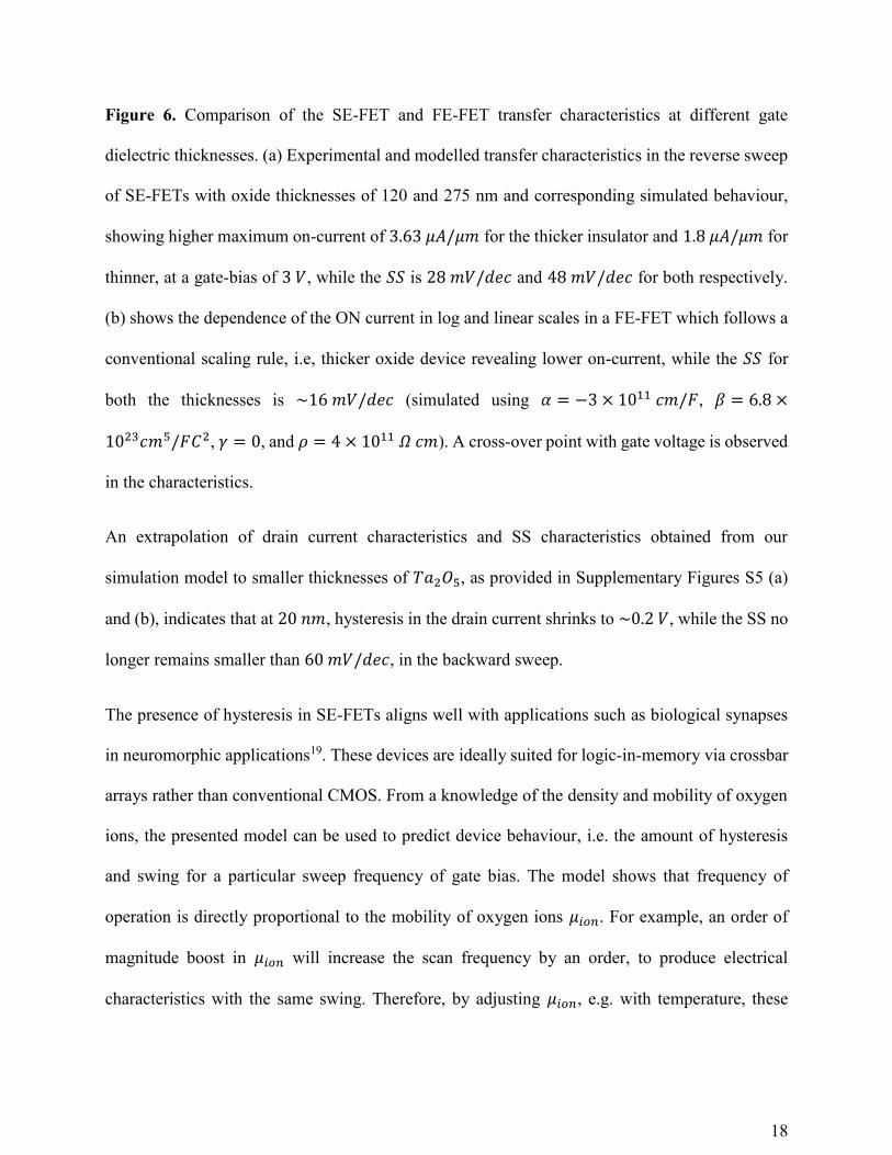
Figure 6. Comparison of the SE-FET and FE-FET transfer characteristics at different gate
dielectric thicknesses. (a) Experimental and modelled transfer characteristics in the reverse sweep
of SE-FETs with oxide thicknesses of 120 and 275 nm and corresponding simulated behaviour,
showing higher maximum on-current of 3.63 𝜇𝐴/𝜇𝑚 for the thicker insulator and 1.8 𝜇𝐴/𝜇𝑚 for
thinner, at a gate-bias of 3 𝑉, while the 𝑆𝑆 is 28 𝑚𝑉/𝑑𝑒𝑐 and 48 𝑚𝑉/𝑑𝑒𝑐 for both respectively.
(b) shows the dependence of the ON current in log and linear scales in a FE-FET which follows a
conventional scaling rule, i.e, thicker oxide device revealing lower on-current, while the 𝑆𝑆 for
both the thicknesses is ~16 𝑚𝑉/𝑑𝑒𝑐 (simulated using 𝛼 = −3 × 10¹¹ 𝑐𝑚/𝐹, 𝛽 = 6.8 ×10²³𝑐𝑚5/𝐹𝐶2, 𝛾 = 0, and 𝜌 = 4 × 10¹¹ 𝛺 𝑐𝑚). A cross-over point with gate voltage is observed
in the characteristics.
An extrapolation of drain current characteristics and SS characteristics obtained from our
simulation model to smaller thicknesses of 𝑇𝑎2𝑂5, as provided in Supplementary Figures S5 (a)
and (b), indicates that at 20 𝑛𝑚, hysteresis in the drain current shrinks to ~0.2 𝑉, while the SS no
longer remains smaller than 60 𝑚𝑉/𝑑𝑒𝑐, in the backward sweep.
The presence of hysteresis in SE-FETs aligns well with applications such as biological synapses
in neuromorphic applications19. These devices are ideally suited for logic-in-memory via crossbar
arrays rather than conventional CMOS. From a knowledge of the density and mobility of oxygen
ions, the presented model can be used to predict device behaviour, i.e. the amount of hysteresis
and swing for a particular sweep frequency of gate bias. The model shows that frequency of
operation is directly proportional to the mobility of oxygen ions 𝜇𝑖𝑜𝑛. For example, an order of
magnitude boost in 𝜇𝑖𝑜𝑛 will increase the scan frequency by an order, to produce electrical
characteristics with the same swing. Therefore, by adjusting 𝜇𝑖𝑜𝑛, e.g. with temperature, these

19
devices can be operated at even higher frequency, e.g. ~1 𝐻𝑧, a desirable frequency in
neuromorphic applications.
CONCLUSION
The theory and mechanism leading to a new class of negative capacitance FETs is unveiled here
using an example of a 𝑇𝑎2𝑂5/𝑍𝑛𝑂 FET. It is shown that the field driven motion of ions and
vacancies in the gate insulator (𝑇𝑎2𝑂5) leads to an accumulation of charge at the interface of the
semiconductor. The dispersion of this charge during the reverse sweep, without any filamentary
process, creates a negative differential capacitance, responsible for steep switching as low as 26 𝑚𝑉/𝑑𝑒𝑐 in the 𝑚𝐻𝑧 range in these devices via a body factor effectively less than unity. Here
we prove irrevocably that the switching behaviour observed in our case, is primarily different from
the mechanism arising from a dual energy landscape responsible for the switching in FE-FETs, by
scrutinising the relationship of 𝑆𝑆 with the frequency in the forward and backward directions.
Distinct characteristics of SE-FET identified in this work demonstrate a representative class of
devices with a solid/liquid electrolyte as gate insulator, whose performance can be tuned via
control of the diffusivity of ions. This class of materials therefore opens up unique opportunities
for optimisation of device performance via control of interfacial phenomena in semiconductor
devices.
ASSOCIATED CONTENT
Supporting Information
The following files are available free of charge.
Derivation of the body factor of the SE-FET; a description of the model of the dynamic transfer
characteristics of the SE-FET; Tables listing the parameters of 𝑍𝑛𝑂 and 𝑇𝑎2𝑂5 used in the model;
Measured device characteristics with temperature highlighting the influence of mobility of ions;

20
Comparison of the simulated transfer characteristics of an SE-FET at two different frequencies
highlighting the influence of ionic motion; Variation of the sheet density of the oxide ions at the 𝑇𝑎2𝑂5/𝑍𝑛𝑂 interface, with gate bias, for different 𝑇𝑎2𝑂5 thickness; Simulated 𝐼𝐷𝑆 − 𝑉𝐺𝑆 and SS
characteristics at different thicknesses of 𝑇𝑎2𝑂5 layer (PDF).
AUTHOR INFORMATION
Corresponding Author
*Email: [email protected]
Author Contributions
M.M.S directed this work to explain the 𝑆𝑆 switching in comparison to FE-FETs including
identification of the key factors such as switching speed, oxide scaling. A.K developed the
equations and undertook the modelling to demonstrate these effects with respect to experimental
data. P.B.P prepared the samples, and characterised the data from measurements, with
contributions from X.S. The manuscript was primarily written by MMS and AK. All authors have
given approval to the final version of the manuscript.
Conflict of Interest
The authors declare no competing financial interests.
ACKNOWLEDGMENT
We gratefully acknowledge funds from the ENIAC JU project E2SG under grant number 296131.
REFERENCES
(1) Datta, S. Quantum Transport : Atom to Transistor; 2005.
(2) Ionescu, A. M.; Riel, H. Tunnel Field-Effect Transistors as Energy-Efficient Electronic

21
Switches. Nature 2011, 479, 329–337.
(3) 2013 ITRS - International Technology Roadmap for Semiconductors.
(4) Nikonov, D. E.; Young, I. A. Overview of Beyond-CMOS Devices and a Uniform
Methodology for Their Benchmarking. Proc. IEEE 2013, 101, 2498–2533.
(5) Jain, A.; Alam, M. A. Prospects of Hysteresis-Free Abrupt Switching (0 MV/Decade) in
Landau Switches. IEEE Trans. Electron Devices 2013, 60, 4269–4276.
(6) Zhirnov, V. V.; Cavin, R. K. Nanoelectronics: Negative Capacitance to the Rescue? Nat.
Nanotechnol. 2008, 3, 77–78.
(7) Park, J. H.; Jang, G. S.; Kim, H. Y.; Seok, K. H.; Chae, H. J.; Lee, S. K.; Joo, S. K. Sub-
KT/q Subthreshold-Slope Using Negative Capacitance in Low-Temperature
Polycrystalline-Silicon Thin-Film Transistor. Sci. Rep. 2016, 6, 24734.
(8) Salahuddin, S.; Datta, S. Use of Negative Capacitance to Provide Voltage Amplification for
Low Power Nanoscale Devices. Nano Lett. 2008, 8, 405–410.
(9) Then, H. W.; Dasgupta, S.; Radosavljevic, M.; Chow, L.; Chu-Kung, B.; Dewey, G.;
Gardner, S.; Gao, X.; Kavalieros, J.; Mukherjee, N.; et al. Experimental Observation and
Physics of “Negative” Capacitance and Steeper than 40mV/Decade Subthreshold Swing in
Al0.83In0.17N/AlN/GaN MOS-HEMT on SiC Substrate. In 2013 IEEE International
Electron Devices Meeting; IEEE, 2013; p. 28.3.1-28.3.4.
(10) Jana, R. K.; Snider, G. L.; Jena, D. On the Possibility of Sub 60 MV/Decade Subthreshold
Switching in Piezoelectric Gate Barrier Transistors. Phys. Status Solidi Curr. Top. Solid
State Phys. 2013, 10, 1469–1472.

22
(11) Loh, O. Y.; Espinosa, H. D. Nanoelectromechanical Contact Switches. Nat. Nanotechnol.
2012, 7, 283–295.
(12) Lee, J. O.; Song, Y.-H.; Kim, M.-W.; Kang, M.-H.; Oh, J.-S.; Yang, H.-H.; Yoon, J.-B. A
Sub-1-Volt Nanoelectromechanical Switching Device. Nat. Nanotechnol. 2013, 8, 36–40.
(13) Kim, J. H.; Chen, Z. C. Y.; Kwon, S.; Xiang, J. Three-Terminal Nanoelectromechanical
Field Effect Transistor with Abrupt Subthreshold Slope. Nano Lett. 2014, 14, 1687–1691.
(14) Shukla, N.; Thathachary, A. V; Agrawal, A.; Paik, H.; Aziz, A.; Schlom, D. G.; Gupta, S.
K.; Engel-Herbert, R.; Datta, S. A Steep-Slope Transistor Based on Abrupt Electronic Phase
Transition. Nat. Commun. 2015, 6, 7812.
(15) Song, J.; Woo, J.; Lee, S.; Prakash, A.; Yoo, J.; Moon, K.; Hwang, H. Steep Slope Field-
Effect Transistors With Ag/TiO 2 -Based Threshold Switching Device. IEEE Electron
Device Lett. 2016, 37, 932–934.
(16) Menzel, S.; Bottger, U.; Wimmer, M.; Salinga, M. Physics of the Switching Kinetics in
Resistive Memories. Adv. Funct. Mater. 2015, 25, 6306–6325.
(17) Tappertzhofen, S.; Valov, I.; Tsuruoka, T.; Hasegawa, T.; Waser, R.; Aono, M. Generic
Relevance of Counter Charges for Cation-Based Nanoscale Resistive Switching Memories.
ACS Nano 2013, 7, 6396–6402.
(18) Wedig, A.; Luebben, M.; Cho, D.-Y.; Moors, M.; Skaja, K.; Rana, V.; Hasegawa, T.;
Adepalli, K. K.; Yildiz, B.; Waser, R.; et al. Nanoscale Cation Motion in TaOx, HfOx and
TiOx Memristive Systems. Nat. Nanotechnol. 2015, 11, 67–74.
(19) Balakrishna Pillai, P.; De Souza, M. M. Nanoionics-Based Three-Terminal Synaptic Device

23
Using Zinc Oxide. ACS Appl. Mater. Interfaces 2017, 9, 1609–1618.
(20) Xu, C.; Xiao, Q.; Ma, J.; Jin, Y.; Shao, J.; Fan, Z. High Temperature Annealing Effect on
Structure, Optical Property and Laser-Induced Damage Threshold of Ta2O5 Films. Appl.
Surf. Sci. 2008, 254, 6554–6559.
(21) Balakrishna Pillai, P.; Kumar, A.; Song, X.; De Souza, M. M. Diffusion-Controlled Faradaic
Charge Storage in High-Performance Solid Electrolyte-Gated Zinc Oxide Thin-Film
Transistors. ACS Appl. Mater. Interfaces 2018, 10, 9782–9791.
(22) Ye, Z.; Yuan, Y.; Xu, H.; Liu, Y.; Luo, J.; Wong, M. Mechanism and Origin of Hysteresis
in Oxide Thin-Film Transistor and Its Application on 3-D Nonvolatile Memory. IEEE
Trans. Electron Devices 2017, 64, 438–446.
(23) Gallagher, P.; Lee, M.; Petach, T. A.; Stanwyck, S. W.; Williams, J. R.; Watanabe, K.;
Taniguchi, T.; Goldhaber-Gordon, D. A High-Mobility Electronic System at an Electrolyte-
Gated Oxide Surface. Nat. Commun. 2015, 6, 6437.
(24) Yoon, J.; Hong, W. K.; Jo, M.; Jo, G.; Choe, M.; Park, W.; Sohn, J. I.; Nedic, S.; Hwang,
H.; Welland, M. E.; et al. Nonvolatile Memory Functionality of ZnO Nanowire Transistors
Controlled by Mobile Protons. ACS Nano 2011, 5, 558–564.
(25) Nasr, B.; Wang, D.; Kruk, R.; Rosner, H.; Hahn, H.; Dasgupta, S. High-Speed, Low-
Voltage, and Environmentally Stable Operation of Electrochemically Gated Zinc Oxide
Nanowire Field-Effect Transistors. Adv. Funct. Mater. 2013, 23, 1750–1758.
(26) Lu, A.; Sun, J.; Jiang, J.; Wan, Q. Low-Voltage Transparent Electric-Double-Layer ZnO-
Based Thin-Film Transistors for Portable Transparent Electronics. Appl. Phys. Lett. 2010,

24
96, 043114.
(27) Shulman, J.; Xue, Y. Y.; Tsui, S.; Chen, F.; Chu, C. W. General Mechanism for Negative
Capacitance Phenomena. Phys. Rev. B - Condens. Matter Mater. Phys. 2009, 80, 1–6.
(28) Gommans, H. H. P.; Kemerink, M.; Janssen, R. A. J. Negative Capacitances in Low-
Mobility Solids. Phys. Rev. B 2005, 72, 235204.
(29) Wang, Y.-F.; Lin, Y.-C.; Wang, I.-T.; Lin, T.-P.; Hou, T.-H. Characterization and Modeling
of Nonfilamentary Ta/TaOx/TiO2/Ti Analog Synaptic Device. Sci. Rep. 2015, 5, 10150.
(30) Mott, N. F.; Gurney, R. W. Electronic Processes in Ionic Crystals; Oxford : Clarendon
Press, 1940.
(31) Kim, S.; Kim, S.-J.; Kim, K. M.; Lee, S. R.; Chang, M.; Cho, E.; Kim, Y.-B.; Kim, C. J.;
Chung, U.-I.; Yoo, I.-K. Physical Electro-Thermal Model of Resistive Switching in Bi-
Layered Resistance-Change Memory. Sci. Rep. 2013, 3, 1680.
(32) Kim, W.; Menzel, S.; Wouters, D. J.; Guo, Y.; Robertson, J.; Roesgen, B.; Waser, R.; Rana,
V. Impact of Oxygen Exchange Reaction at the Ohmic Interface in Ta2O5-Based ReRAM
Devices. Nanoscale 2016, 8, 17774–17781.
(33) Liu, C. M.; Liu, W. L.; Chen, W. J.; Hsieh, S. H.; Tsai, T. K.; Yang, L. C. ITO as a Diffusion
Barrier Between Si and Cu. J. Electrochem. Soc. 2005, 152, G234–G239.
(34) Lee, S. T.; Gao, Z. Q.; Hung, L. S. Metal Diffusion from Electrodes in Organic Light-
Emitting Diodes. Appl. Phys. Lett. 1999, 75, 1404–1406.
(35) Schlatmann, A. R.; Floet, D. W.; Hilberer, A.; Garten, F.; Smulders, P. J. M.; Klapwijk, T.

25
M.; Hadziioannou, G. Indium Contamination from the Indium-Tin-Oxide Electrode in
Polymer Light-Emitting Diodes. Appl. Phys. Lett. 1996, 69, 1764–1766.
(36) Bard, A. J.; Faulkner, L. R. Electrochemical Methods: Fundamentals and Applications;
Wiley, 2001.
(37) Moors, M.; Adepalli, K. K.; Lu, Q.; Wedig, A.; Bäumer, C.; Skaja, K.; Arndt, B.; Tuller, H.
L.; Dittmann, R.; Waser, R.; et al. Resistive Switching Mechanisms on TaO x and SrRuO
3 Thin-Film Surfaces Probed by Scanning Tunneling Microscopy. ACS Nano 2016, 10,
1481–1492.
(38) Valov, I.; Linn, E.; Tappertzhofen, S.; Schmelzer, S.; van den Hurk, J.; Lentz, F.; Waser,
R. Nanobatteries in Redox-Based Resistive Switches Require Extension of Memristor
Theory. Nat. Commun. 2013, 4, 1771.
(39) Lübben, M.; Karakolis, P.; Ioannou-Sougleridis, V.; Normand, P.; Dimitrakis, P.; Valov, I.
Graphene-Modified Interface Controls Transition from VCM to ECM Switching Modes in
Ta/TaO x Based Memristive Devices. Adv. Mater. 2015, 27, 6202–6207.
(40) Siemon, A.; Breuer, T.; Aslam, N.; Ferch, S.; Kim, W.; Van Den Hurk, J.; Rana, V.;
Hoffmann-Eifert, S.; Waser, R.; Menzel, S.; et al. Realization of Boolean Logic
Functionality Using Redox-Based Memristive Devices. Adv. Funct. Mater. 2015, 25, 6414–
6423.
(41) Skaja, K.; Bäumer, C.; Peters, O.; Menzel, S.; Moors, M.; Du, H.; Bornhöfft, M.; Schmitz,
C.; Feyer, V.; Jia, C. L.; et al. Avalanche-Discharge-Induced Electrical Forming in
Tantalum Oxide-Based Metal-Insulator-Metal Structures. Adv. Funct. Mater. 2015, 25,

26
7154–7162.
(42) Duarte, J. P.; Khandelwal, S.; Khan, A. I.; Sachid, A.; Lin, Y.; Chang, H.; Salahuddin, S.;
Hu, C. Compact Models of Negative-Capacitance FinFETs: Lumped and Distributed
Charge Models. In 2016 IEEE International Electron Devices Meeting (IEDM); IEEE,
2016; Vol. 5, p. 30.5.1-30.5.4.
TABLE OF CONTENTS FIGURE


![Sangeetha [Ferroelectric Memory]](https://static.fdocuments.net/doc/165x107/55cf8f91550346703b9d9665/sangeetha-ferroelectric-memory.jpg)