Alberto Caviglia & Enrico Costa Crossed nanotube Junctions M. S. Fuhrer, J. Nygård, L. Shih, M....
55
Alberto Caviglia & Enri Alberto Caviglia & Enri co Costa co Costa Crossed nanotube Crossed nanotube Junctions Junctions M. S. Fuhrer, J. Nygård, L. Shih, M. Forero, M. S. Fuhrer, J. Nygård, L. Shih, M. Forero, Young-Gui Yoon, Young-Gui Yoon, M. S. C. Mazzoni, Hyoung Joon Choi, Jisoon Ihm, M. S. C. Mazzoni, Hyoung Joon Choi, Jisoon Ihm, Steven G. Louie, A. Zettl, Paul L. McEuen Steven G. Louie, A. Zettl, Paul L. McEuen
-
Upload
monica-marion-jackson -
Category
Documents
-
view
215 -
download
0
Transcript of Alberto Caviglia & Enrico Costa Crossed nanotube Junctions M. S. Fuhrer, J. Nygård, L. Shih, M....

Alberto Caviglia & Enrico CostaAlberto Caviglia & Enrico Costa
Crossed nanotube Crossed nanotube JunctionsJunctions
M. S. Fuhrer, J. Nygård, L. Shih, M. Forero, Young-Gui M. S. Fuhrer, J. Nygård, L. Shih, M. Forero, Young-Gui Yoon,Yoon,
M. S. C. Mazzoni, Hyoung Joon Choi, Jisoon Ihm,M. S. C. Mazzoni, Hyoung Joon Choi, Jisoon Ihm,Steven G. Louie, A. Zettl, Paul L. McEuenSteven G. Louie, A. Zettl, Paul L. McEuen

Alberto Caviglia & Enrico CostaAlberto Caviglia & Enrico Costa
Presentation byPresentation by Alberto Caviglia & Enrico Alberto Caviglia & Enrico
CostaCosta
for the course offor the course of
Nanotecnologie 1Nanotecnologie 1
held by held by
Prof. Ermanno Di ZittiProf. Ermanno Di Zitti

Alberto Caviglia & Enrico CostaAlberto Caviglia & Enrico Costa 33
Crossed nanotubes junctionsCrossed nanotubes junctions
IntroductionIntroduction
SINGLE-WALLED carbon nanotubes (SWNTs) areSINGLE-WALLED carbon nanotubes (SWNTs) are
nanometer-diameter cylinders consisting of a singlenanometer-diameter cylinders consisting of a single
graphene sheet wrapped up to form a tube. graphene sheet wrapped up to form a tube.
Since their discovery in the early 1990s, there has beenSince their discovery in the early 1990s, there has been
intense activity exploring the electrical properties ofintense activity exploring the electrical properties of
these systems and their potential applications inthese systems and their potential applications in
electronics.electronics.

Alberto Caviglia & Enrico CostaAlberto Caviglia & Enrico Costa 44
Crossed nanotubes junctionsCrossed nanotubes junctions
Growth of SWNT (1)Growth of SWNT (1)(J. Phys. Chem. B, Vol. 103, No. 51,1999 pg 11246)(J. Phys. Chem. B, Vol. 103, No. 51,1999 pg 11246)
The principal methods for obtaining high-quality single-walled nanotube are arc discharge and laser vaporization.
Both methods involve evaporating carbon atoms from solid carbon sources at ≥3000 °C, which limits the scale-up of SWNTs.
Nanotubes synthesized by the evaporation methods are in tangled forms that are difficult to purify, manipulate, and assemble for building addressable nanotubes architectures.

Alberto Caviglia & Enrico CostaAlberto Caviglia & Enrico Costa 55
Crossed nanotubes junctionsCrossed nanotubes junctions
Arc discharge(http://students.chem.tue.nl/ifp03/synthesis.html#_Toc33936434)
A direct current of 50 to 100 A driven by approximately 20 V DC A direct current of 50 to 100 A driven by approximately 20 V DC creates a high temperature discharge between the two electrodes.creates a high temperature discharge between the two electrodes.
The discharge vaporises one of the carbon rods and forms a small rod The discharge vaporises one of the carbon rods and forms a small rod shaped deposit on the other rod. shaped deposit on the other rod.

Alberto Caviglia & Enrico CostaAlberto Caviglia & Enrico Costa 66
Crossed nanotubes junctionsCrossed nanotubes junctions
Laser vaporisationLaser vaporisation(http://students.chem.tue.nl/ifp03/synthesis.html#_Toc33936434)
The laser vaporisation apparatus used by Smalley's The laser vaporisation apparatus used by Smalley's group is used to vaporise a graphite target in an oven group is used to vaporise a graphite target in an oven at 1200 °C. at 1200 °C.

Alberto Caviglia & Enrico CostaAlberto Caviglia & Enrico Costa 77
Crossed nanotubes junctionsCrossed nanotubes junctions
Growth of SWNT (2)Growth of SWNT (2)(78 IEEE Transaction on nanotechnology, VOL. 1, N° 1, March 2002, pg.80)(78 IEEE Transaction on nanotechnology, VOL. 1, N° 1, March 2002, pg.80)
((a) Schematic of a SWNT a) Schematic of a SWNT growing from a catalyst seed growing from a catalyst seed particle. particle.
(b) Atomic force microscope (b) Atomic force microscope images of a single nanotube images of a single nanotube device fabricated using electron device fabricated using electron beam lithography. beam lithography.

Alberto Caviglia & Enrico CostaAlberto Caviglia & Enrico Costa 88
Crossed nanotubes junctionsCrossed nanotubes junctions
Chemical vapor deposition(J. Phys. Chem. B, Vol. 103, No. 51,1999,pg.11248)(J. Phys. Chem. B, Vol. 103, No. 51,1999,pg.11248)
Chemical vapor deposition methods have been very successful in synthesizing carbon fibers, filaments.
CVD synthesis of high-quality SWNTs is only recent by using methane as carbon feedstock and iron oxide nanoparticles supported on high surface area alumina as the catalyst.
It is found that methane is stable at the elevated growth temperatures without appreciable self-pyrolysis.

Alberto Caviglia & Enrico CostaAlberto Caviglia & Enrico Costa 99
Crossed nanotubes junctionsCrossed nanotubes junctions
Methane importance(J. Phys. Chem. B, Vol. 103, No. 51,1999,pg.11248)(J. Phys. Chem. B, Vol. 103, No. 51,1999,pg.11248)
The methane stability prevents the formation of amorphous carbon that tends to cause catalyst poisoning and overcoating of the nanotubes.
The chemical and textural properties of the catalyst materials dictate the yield and quality of SWNTs.
The diameters of the SWNTs are dispersed in the range 0.7-5 nm with a peak at 1.7 nm.

Alberto Caviglia & Enrico CostaAlberto Caviglia & Enrico Costa 1010
Crossed nanotubes junctionsCrossed nanotubes junctions
SWNT imageSWNT image(J. Phys. Chem. B, Vol. 103, No. 51,1999, pg.11248)(J. Phys. Chem. B, Vol. 103, No. 51,1999, pg.11248)
On the left the TEM image of SWNTs synthesized in bulk.

Alberto Caviglia & Enrico CostaAlberto Caviglia & Enrico Costa 1111
Crossed nanotubes junctionsCrossed nanotubes junctions
SWNT purification methods (1)SWNT purification methods (1)(“Fullerene Pipes” R.E. Smalley et al. Science 280, 1998 pg.1253)(“Fullerene Pipes” R.E. Smalley et al. Science 280, 1998 pg.1253)
In a typical procedure, a raw sample of nanotubes (8.5 g) was first refluxed in 1.2 liters of 2.6 M nitric acid for 45 hours.
Upon cooling, the solution was transferred to polytetrafluoroethylene centrifuge tubes and spun at 2400g for 2 hours.
The supernatant acid was decanted off, replaced by deionized water, and vigorously shaken to resuspend the solids, followed by a second centrifuge-decant cycle.

Alberto Caviglia & Enrico CostaAlberto Caviglia & Enrico Costa 1212
Crossed nanotubes junctionsCrossed nanotubes junctions
SWNT purification methods (2)SWNT purification methods (2)(“Fullerene Pipes” R.E. Smalley et al. Science 280, 1998 pg.1253)(“Fullerene Pipes” R.E. Smalley et al. Science 280, 1998 pg.1253)
The solids were resuspended in 1.8 liters of water with 20 ml of Triton X-100 surfactant (Aldrich) and adjusted to pH 10 with sodium hydroxide.
The suspension was then transferred to the reservoir of a tangential flow filtration system (MiniKros Lab System; Spectrum, Laguna Hills, CA).
The cartridge inlet pressure was maintained at 6 psi. A control valve was added to the exit so that the outflow rate was restricted to 70 ml min-1.

Alberto Caviglia & Enrico CostaAlberto Caviglia & Enrico Costa 1313
Crossed nanotubes junctionsCrossed nanotubes junctions
SWNTs usageSWNTs usage
Experiments and theory have shown that these Experiments and theory have shown that these tubes can be either metals or semiconductors, tubes can be either metals or semiconductors, depending on their chirality and their electrical depending on their chirality and their electrical properties can rival, or even exceed, the best properties can rival, or even exceed, the best metals or semiconductors known.metals or semiconductors known.
Individual SWNTs may act as device such as Individual SWNTs may act as device such as field-effect transistors , single-electron-tunneling field-effect transistors , single-electron-tunneling transistors or rectifiers.transistors or rectifiers.

Alberto Caviglia & Enrico CostaAlberto Caviglia & Enrico Costa 1414
Crossed nanotubes junctionsCrossed nanotubes junctions
Problems to solveProblems to solve
How can individual SWNTs be joined together How can individual SWNTs be joined together to form multimedial devices and, ultimately, to form multimedial devices and, ultimately, complex circuits ?complex circuits ?
How can, in particular, SWNT-SWNT How can, in particular, SWNT-SWNT junctions, formed by nanotubes that lie across junctions, formed by nanotubes that lie across one another on a substrate, be used to solve the one another on a substrate, be used to solve the previous question ?previous question ?
Alberto Caviglia & Enrico CostaAlberto Caviglia & Enrico Costa 1515
Crossed nanotubes junctionsCrossed nanotubes junctions
SWNT SWNT junctionsSWNT SWNT junctions
Consist of two crossed individual SWNT’s or Consist of two crossed individual SWNT’s or small bundles (diameter<3nm) of SWNTs with small bundles (diameter<3nm) of SWNTs with four electrical contacts, one on each end of each four electrical contacts, one on each end of each SWNT or bundle.SWNT or bundle.
This type of junction is easily constructed and, This type of junction is easily constructed and, with the development of techniques to place with the development of techniques to place nanotubes with precision on substrates, could be nanotubes with precision on substrates, could be mass produced.mass produced.

Alberto Caviglia & Enrico CostaAlberto Caviglia & Enrico Costa 1616
Crossed nanotubes junctionsCrossed nanotubes junctions
Image of the deviceImage of the device
On the left we can see the On the left we can see the atomic force microscope atomic force microscope (AFM) image of a (AFM) image of a completed crossed completed crossed nanotube device.nanotube device.
Two crossed SWNTs Two crossed SWNTs (green) interconnect the (green) interconnect the Cr/Au contacts (yellow). Cr/Au contacts (yellow).

Alberto Caviglia & Enrico CostaAlberto Caviglia & Enrico Costa 1717
Crossed nanotubes junctionsCrossed nanotubes junctions
Gate voltageGate voltage(J. Phys. Chem. B, Vol. 103, No. 51,1999,pg.11248)(J. Phys. Chem. B, Vol. 103, No. 51,1999,pg.11248)
A gate voltage VA gate voltage Vgg can be applied to the substrate can be applied to the substrate
to change the charge density per unit length.to change the charge density per unit length.

Alberto Caviglia & Enrico CostaAlberto Caviglia & Enrico Costa 1818
Crossed nanotubes junctionsCrossed nanotubes junctions
Dependence by gate Dependence by gate voltagevoltage
At room temperature the two type of SWNTs have At room temperature the two type of SWNTs have
different behavior .different behavior .
Metallic SWNTs have a finite conductance that is nearly independent of Vg.
Semiconducting Semiconducting SWNTs are found to be SWNTs are found to be p-type:p-type:Conducting for VConducting for Vgg<0<0Insulating for VInsulating for Vgg>0>0

Alberto Caviglia & Enrico CostaAlberto Caviglia & Enrico Costa 1919
Crossed nanotubes junctionsCrossed nanotubes junctions
SWNTSWNT composition composition Crossed SWNT can be Crossed SWNT can be
composed of:composed of: Two metallic SWNTs Two metallic SWNTs
(MM)(MM) One metallic and one One metallic and one
semiconducting (MS)semiconducting (MS) Two semiconducting Two semiconducting
SWNTs (SS)SWNTs (SS)

Alberto Caviglia & Enrico CostaAlberto Caviglia & Enrico Costa 2020
Crossed nanotubes junctionsCrossed nanotubes junctions
MM junctionsMM junctions In a MM junctions result that, if G is the conductance:In a MM junctions result that, if G is the conductance:
G G junctionjunction ≈ G ≈ G individual tubeindividual tube

Alberto Caviglia & Enrico CostaAlberto Caviglia & Enrico Costa 2121
Crossed nanotubes junctionsCrossed nanotubes junctions
Mesure of the conductancesMesure of the conductances In order to measure the In order to measure the
four-terminal four-terminal conductances and so conductances and so accurately determinate accurately determinate the junction conductance, the junction conductance, current is passed, for current is passed, for example, into the 1->3 example, into the 1->3 circuit and the contactcircuit and the contact 2 & 4 act as probe 2 & 4 act as probe. .

Alberto Caviglia & Enrico CostaAlberto Caviglia & Enrico Costa 2222
Crossed nanotubes junctionsCrossed nanotubes junctions
Landauer-Buttiker Formula (1)Landauer-Buttiker Formula (1)(78 IEEE Transaction on nanotechnology, VOL. 1, N° 1, March 2002, pg.78)(78 IEEE Transaction on nanotechnology, VOL. 1, N° 1, March 2002, pg.78)
The two terminal Landauer-Buttiker formula states The two terminal Landauer-Buttiker formula states that, for a system with N 1-D channels in parallel: that, for a system with N 1-D channels in parallel: G= (NeG= (Ne22/h)T, where T is the transmission coefficient /h)T, where T is the transmission coefficient for electrons through the sample.for electrons through the sample.
For a SWNT at low doping levels such that only one For a SWNT at low doping levels such that only one transverse sub-band is occupied, N=4. Each channel transverse sub-band is occupied, N=4. Each channel is fourfold degenerate, due to spin degeneracy and is fourfold degenerate, due to spin degeneracy and the sublattice degeneracy of electrons in graphene.the sublattice degeneracy of electrons in graphene.

Alberto Caviglia & Enrico CostaAlberto Caviglia & Enrico Costa 2323
Crossed nanotubes junctionsCrossed nanotubes junctions
Landauer-Buttiker Formula (2)Landauer-Buttiker Formula (2)(78 IEEE Transaction on nanotechnology, VOL. 1, N° 1, March 2002, pg.78)(78 IEEE Transaction on nanotechnology, VOL. 1, N° 1, March 2002, pg.78)
The conductance of ballistic SWNT with perfect The conductance of ballistic SWNT with perfect contacts (T=1) is then 4econtacts (T=1) is then 4e22/h = 155 /h = 155 µS, or about 6.5 kµS, or about 6.5 kΩΩ..
Two-terminal conductances of metallic SWNTs at Two-terminal conductances of metallic SWNTs at room temperature can vary significantly, ranging from room temperature can vary significantly, ranging from as small as ~ 6 kas small as ~ 6 kΩΩ to many Mto many MΩΩ. .
Most of this variation is due to variations in contact Most of this variation is due to variations in contact resistance between the electrodes and the tube. resistance between the electrodes and the tube.
The best contacts have been obtained by evaporating The best contacts have been obtained by evaporating Au or Pt over the tube, often followed by a subsequent Au or Pt over the tube, often followed by a subsequent anneal. anneal.

Alberto Caviglia & Enrico CostaAlberto Caviglia & Enrico Costa 2424
Crossed nanotubes junctionsCrossed nanotubes junctions
Measured conductancesMeasured conductances At 200K the slope of I-V At 200K the slope of I-V
shown in the figure shown in the figure corresponds to:corresponds to:
G = 0.13 eG = 0.13 e22/h/h Other MM junctions gave Other MM junctions gave
the following value :the following value : G = 0,086 eG = 0,086 e22/h/h G = 0,120 eG = 0,120 e22/h/h G = 0,260 eG = 0,260 e22/h/h

Alberto Caviglia & Enrico CostaAlberto Caviglia & Enrico Costa 2525
Crossed nanotubes junctionsCrossed nanotubes junctions
Transmission probababilityTransmission probabability The transmission The transmission probabilityprobability for the junction is:for the junction is:
T = G/(4eT = G/(4e22/h)/h) The previous values of G gave that:The previous values of G gave that:
0.02 <0.02 < TTj j < 0.06< 0.06 MM junctions make surprisingly good tunnel MM junctions make surprisingly good tunnel
contacts, despite the extremely small junction area contacts, despite the extremely small junction area (on the order of 1 nm(on the order of 1 nm22).).

Alberto Caviglia & Enrico CostaAlberto Caviglia & Enrico Costa 2626
Crossed nanotubes junctionsCrossed nanotubes junctions
Other configurationsOther configurations
For two SWMTs with For two SWMTs with wrapping indices (5,5) wrapping indices (5,5) separated by the Van der separated by the Van der Waals distance of 0,34 Waals distance of 0,34 nm experiments gave:nm experiments gave:
TTj j ≈ 2 x 10≈ 2 x 10⁻⁴-4

Alberto Caviglia & Enrico CostaAlberto Caviglia & Enrico Costa 2727
Crossed nanotubes junctionsCrossed nanotubes junctions
Crossed junction composition (1) If the nanotubes interact If the nanotubes interact
with the SiO substrate with the SiO substrate included, they deforms included, they deforms significantly at the junction.significantly at the junction.
In a following article (Structural Deformation and Intertube Conductance of Crossed Carbon Nanotube Junctions) is performed a study of the conductance as a function of the contact force.

Alberto Caviglia & Enrico CostaAlberto Caviglia & Enrico Costa 2828
Crossed nanotubes junctionsCrossed nanotubes junctions
Crossed junction composition (2) In a crossed junction composed of SWNTs:
for a diameter of 1.4 nm, this contact force must be about 5 nN.
for a diameter of 5.5 nm, this contact force has been estimated to be about 15 nN
The junction geometry is determined by performing a constrained total energy minimization in a supercell, in which they fully relax the position of the atoms near the junction while fixing the center-to-center intertube distance at the boundaries to produce the desired contact force.

Alberto Caviglia & Enrico CostaAlberto Caviglia & Enrico Costa 2929
Crossed nanotubes junctionsCrossed nanotubes junctions
Crossed junction composition (3)
The structure needs to be accurate, since the interatomic in the experimental devices, they expect that the strong adhesion of the SWNTs to the SiO2 substrate generates a significant contact force between the two crossed SWNTs.
In this case:
Tj ≈ 0,04

Alberto Caviglia & Enrico CostaAlberto Caviglia & Enrico Costa 3030
Crossed nanotubes junctionsCrossed nanotubes junctions
Charge density in MM Charge density in MM SWNTsSWNTs
The charge density in the contact region became The charge density in the contact region became sizeable as the nanotubes became closer and more sizeable as the nanotubes became closer and more deformed, resulting from a significant overlap of deformed, resulting from a significant overlap of intertube wave function.intertube wave function.

Alberto Caviglia & Enrico CostaAlberto Caviglia & Enrico Costa 3131
Crossed nanotubes junctionsCrossed nanotubes junctions
SS junctions (1)SS junctions (1)
The measurement of SS junctions are complicated The measurement of SS junctions are complicated by the often very resistive contacts to by the often very resistive contacts to semiconducting SWNTs.semiconducting SWNTs.
The SS junction, like MM junctions, make The SS junction, like MM junctions, make
relatively good tunnel contactsrelatively good tunnel contacts..

Alberto Caviglia & Enrico CostaAlberto Caviglia & Enrico Costa 3232
Crossed nanotubes junctionsCrossed nanotubes junctions
SS junctions (2)SS junctions (2) The two terminal The two terminal
conductances of SS conductances of SS junctions measure at junctions measure at 200 K give:200 K give: G = 0.011 eG = 0.011 e22/h/h G = 0.06 eG = 0.06 e22/h/h
In the figure on the left In the figure on the left is represented the is represented the higher measure with higher measure with open circles.open circles.

Alberto Caviglia & Enrico CostaAlberto Caviglia & Enrico Costa 3333
Crossed nanotubes junctionsCrossed nanotubes junctions
MM & SS comparison MM & SS comparison In the two figures are represented In the two figures are represented
the expected band structures near the expected band structures near the junctions of the MM & SS. the junctions of the MM & SS.
Both junctions are expected to Both junctions are expected to have a finite density of states have a finite density of states available for tunneling on either available for tunneling on either side of the junction. side of the junction.

Alberto Caviglia & Enrico CostaAlberto Caviglia & Enrico Costa 3434
Crossed nanotubes junctionsCrossed nanotubes junctions
MS junctions (1)MS junctions (1) In this case charge transfer at the junction between a In this case charge transfer at the junction between a
dropped semiconducting SWNT and a metallic dropped semiconducting SWNT and a metallic SWNT is expected to form a Schottky barrier.SWNT is expected to form a Schottky barrier.
Semiconducting & metallic SWNTs both share the Semiconducting & metallic SWNTs both share the same graphene band structure.same graphene band structure.

Alberto Caviglia & Enrico CostaAlberto Caviglia & Enrico Costa 3535
Crossed nanotubes junctionsCrossed nanotubes junctions
MS junctions (2)MS junctions (2)
The Fermi level EThe Fermi level EF F of the metallic SWNT should align of the metallic SWNT should align
within the band gap of the semiconducting SWNT at within the band gap of the semiconducting SWNT at the junction, depleting the doping of the the junction, depleting the doping of the semiconducting SWNT at the junction.semiconducting SWNT at the junction.
EEFF far for the junction is in the valence band of the far for the junction is in the valence band of the
semiconducting SWNT.semiconducting SWNT.

Alberto Caviglia & Enrico CostaAlberto Caviglia & Enrico Costa 3636
Crossed nanotubes junctionsCrossed nanotubes junctions
Total barrier transmission Total barrier transmission probability probability
The depletion region in the semiconducting SWNT The depletion region in the semiconducting SWNT associated with the Schottky barrier represent an associated with the Schottky barrier represent an additional tunneling barrier.additional tunneling barrier.
The total barrier transmission probability is given by:The total barrier transmission probability is given by:
TTMSMS = T = Tj j TTdd
where:where: Td is the transmission probability for tunneling through the
depletion region to the location of the metal SWNT Tj is the probability of tunneling between the SWNTs

Alberto Caviglia & Enrico CostaAlberto Caviglia & Enrico Costa 3737
Crossed nanotubes junctionsCrossed nanotubes junctions
MS conductance (1)MS conductance (1) The I-V curves for two The I-V curves for two
MS junctions, measured MS junctions, measured at a temperature of 50 K at a temperature of 50 K and Vand Vgg = -25 V is shown = -25 V is shown in the figure.in the figure.
The low-bias The low-bias conductances are for both conductances are for both devices:devices:
TTMSMS ≈ 2 x 10 ≈ 2 x 10⁻⁴-4

Alberto Caviglia & Enrico CostaAlberto Caviglia & Enrico Costa 3838
Crossed nanotubes junctionsCrossed nanotubes junctions
MS conductance (2)MS conductance (2)
So ifSo if
TTj j = 0.04 (as the MS case)= 0.04 (as the MS case)
then must be:then must be:
TTdd = 5 x 10 = 5 x 10⁻³-3
This is in agreement with a recent calculation by This is in agreement with a recent calculation by Odintsov and a corresponding depletion width of 7 Odintsov and a corresponding depletion width of 7 nm, for a similar doping level.nm, for a similar doping level.

Alberto Caviglia & Enrico CostaAlberto Caviglia & Enrico Costa 3939
Crossed nanotubes junctionsCrossed nanotubes junctions
MS I-V characteristicsMS I-V characteristics The I-V characteristics of The I-V characteristics of
the two MS devices are the two MS devices are here shown over an here shown over an expanded bias range.expanded bias range.
The dotted lines are linear The dotted lines are linear fits to the forward bias fits to the forward bias data (bias applied to the data (bias applied to the semiconducting SWNT).semiconducting SWNT).

Alberto Caviglia & Enrico CostaAlberto Caviglia & Enrico Costa 4040
Crossed nanotubes junctionsCrossed nanotubes junctions
Forward bias Forward bias comportament (1)comportament (1)
The conductance grows with The conductance grows with increasing bias and is greater for increasing bias and is greater for positive biases applied to the positive biases applied to the semiconducting SWNT than for semiconducting SWNT than for negative biases.negative biases.
The forward bias I-V curve The forward bias I-V curve saturates to a linear behavior.saturates to a linear behavior.

Alberto Caviglia & Enrico CostaAlberto Caviglia & Enrico Costa 4141
Crossed nanotubes junctionsCrossed nanotubes junctions
Forward bias Forward bias comportament (2)comportament (2)
The V intercept of the linear region gives a measure of the The V intercept of the linear region gives a measure of the barrier height for the two devices: barrier height for the two devices:
EEbarrier1barrier1 = 190 meV = 190 meV
EEbarrier2barrier2 = 290 meV = 290 meV
This value agrees with the expected value for 1 to 1.5 nm This value agrees with the expected value for 1 to 1.5 nm semiconducting SWNTs :semiconducting SWNTs :
EEbarrierbarrier = E = Egg/2/2
500 meV<E500 meV<Egg<700 meV<700 meV
So: 250meV<ESo: 250meV<Ebarrierbarrier<350 meV<350 meV

Alberto Caviglia & Enrico CostaAlberto Caviglia & Enrico Costa 4242
Crossed nanotubes junctionsCrossed nanotubes junctions
Reverse bias comportamentReverse bias comportament
Reverse biases increase the Reverse biases increase the Schottky barrier, but because the Schottky barrier, but because the depletion region is small, depletion region is small, tunneling still occurs through the tunneling still occurs through the barrier and leads to a measurable barrier and leads to a measurable current flow that increase with current flow that increase with increasing reverse bias.increasing reverse bias.

Alberto Caviglia & Enrico CostaAlberto Caviglia & Enrico Costa 4343
Crossed nanotubes junctionsCrossed nanotubes junctions
G through a semiconducting G through a semiconducting SWNT (1)SWNT (1)
As shown in the figure (bias = 0), carriers charge As shown in the figure (bias = 0), carriers charge in the depletion region in the semiconducting in the depletion region in the semiconducting SWNT must pass a barrier twice as wide as in SWNT must pass a barrier twice as wide as in tunneling to the metallic SWNT. tunneling to the metallic SWNT.

Alberto Caviglia & Enrico CostaAlberto Caviglia & Enrico Costa 4444
Crossed nanotubes junctionsCrossed nanotubes junctions
G through a semiconducting G through a semiconducting SWNT (2)SWNT (2)
The semiconducting SWNT contains two barriers, The semiconducting SWNT contains two barriers, each with transmission probability Td, corresponding each with transmission probability Td, corresponding to the depletion regions in the semiconducting SWNT to the depletion regions in the semiconducting SWNT on either side of the metallic SWNT. on either side of the metallic SWNT.
The total direct transmission through the The total direct transmission through the semiconducting SWNT is thensemiconducting SWNT is then::
TTss ≈ T ≈ T22dd

Alberto Caviglia & Enrico CostaAlberto Caviglia & Enrico Costa 4545
Crossed nanotubes junctionsCrossed nanotubes junctions
MeasureMeasure of of TTs s (1)(1) To determinate TTo determinate Ts, s,
excluding the process excluding the process that involve the metal, it that involve the metal, it used the device used the device geometry shown in the geometry shown in the figure.figure.
A voltage V was applied A voltage V was applied to one end of the to one end of the semiconducting SWNT semiconducting SWNT in a MS device.in a MS device.

Alberto Caviglia & Enrico CostaAlberto Caviglia & Enrico Costa 4646
Crossed nanotubes junctionsCrossed nanotubes junctions
MeasureMeasure of of TTs s (2)(2)
The other end was The other end was grounded through a grounded through a current-measuring current-measuring amplifier.amplifier.
The metallic SWNT The metallic SWNT was grounded through a was grounded through a second amplifier to second amplifier to measure Imeasure IMM

Alberto Caviglia & Enrico CostaAlberto Caviglia & Enrico Costa 4747
Crossed nanotubes junctionsCrossed nanotubes junctions
DeterminationDetermination of T of Td d valuevalue The linear response conductance across the
semiconducting SWNT is 4.3 nS, corresponding to a transmission probability
Ts = 2.8 x 10⁻⁵. This indicates that:
Td ≈ (Ts)1/2 ≈ 5.3 x 10⁻³
in excellent agreement with the two-terminal result obtained earlier:
Td = 5.3 x 10⁻³

Alberto Caviglia & Enrico CostaAlberto Caviglia & Enrico Costa 4848
Crossed nanotubes junctionsCrossed nanotubes junctions
Three-terminal behavior (1)Three-terminal behavior (1) The test circuit is the same of the determination of TThe test circuit is the same of the determination of Ts.s.
Two cases are possible:Two cases are possible: VVbiasbias <0 : the barrier to holes will remain intact, because <0 : the barrier to holes will remain intact, because
the metallic SWNT remains at roughly the same the metallic SWNT remains at roughly the same potential as the grounded end of the semiconducting potential as the grounded end of the semiconducting SWNT.SWNT.
Alberto Caviglia & Enrico CostaAlberto Caviglia & Enrico Costa 4949
Crossed nanotubes junctionsCrossed nanotubes junctions
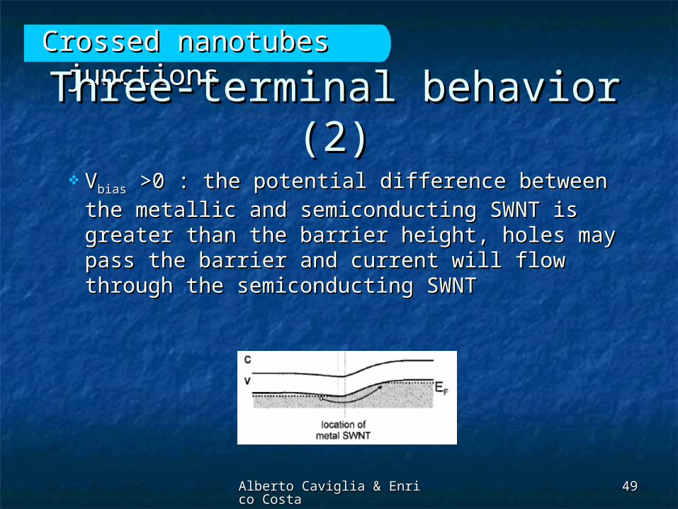
Three-terminal behavior (2)Three-terminal behavior (2)
VVbiasbias >0 : the potential difference between the metallic >0 : the potential difference between the metallic
and semiconducting SWNT is greater than the barrier and semiconducting SWNT is greater than the barrier height, holes may pass the barrier and current will height, holes may pass the barrier and current will flow through the semiconducting SWNTflow through the semiconducting SWNT

Alberto Caviglia & Enrico CostaAlberto Caviglia & Enrico Costa 5050
Crossed nanotubes junctionsCrossed nanotubes junctions
Relation between IRelation between Iss and V and Vbiasbias
For
-700mV <Vbias< 700mV
the current from the semiconducting SWNT is approximately 100 times greater.
The direction of the rectification is determined by the contact of the semiconducting SWNT to which the metal SWNT is connected.

Alberto Caviglia & Enrico CostaAlberto Caviglia & Enrico Costa 5151
Crossed nanotubes junctionsCrossed nanotubes junctions
ConclusionsConclusions It has been noted that the ineffective screening
inherent in one-dimensional systems poses problems for nanotube Schottky devices: Nanometer-scale depletion regions are likely to be leaky barriers to tunneling.
The existence of a third terminal in their MS junction device offer a solution to this problem, allowing to construct a good rectifier from narrow Schottky barriers.

Alberto Caviglia & Enrico CostaAlberto Caviglia & Enrico Costa 5252
Crossed nanotubes junctionsCrossed nanotubes junctions
Conclusions (2)Conclusions (2)
The active length of the device is on the order of 15 nm, demonstrating that useful devices consisting of only a few thousands of atoms can be constructed from SWNTs

Alberto Caviglia & Enrico CostaAlberto Caviglia & Enrico Costa 5353
Crossed nanotubes junctionsCrossed nanotubes junctions
Challenges and future Challenges and future prospects (1)prospects (1)
(78 IEEE Transaction on nanotechnology, VOL. 1, N° 1, March 2002, pg.83)(78 IEEE Transaction on nanotechnology, VOL. 1, N° 1, March 2002, pg.83)
Metallic tubes have conductivities and current Metallic tubes have conductivities and current densities that meet or exceed the best metals.densities that meet or exceed the best metals.
Semiconducting tubes have mobilities and Semiconducting tubes have mobilities and transconductances that meet or exceed the best transconductances that meet or exceed the best semiconductor.semiconductor.
Nanotube electronic devices function perfectly well Nanotube electronic devices function perfectly well under biological condictions and have dimensions under biological condictions and have dimensions comparable to typical biomolecules.comparable to typical biomolecules.

Alberto Caviglia & Enrico CostaAlberto Caviglia & Enrico Costa 5454
Crossed nanotubes junctionsCrossed nanotubes junctions
Challenges and future Challenges and future prospects (2)prospects (2)
(78 IEEE Transaction on nanotechnology, VOL. 1, N° 1, March 2002, pg.83)(78 IEEE Transaction on nanotechnology, VOL. 1, N° 1, March 2002, pg.83)
Issue of device manufacturability. Issue of device manufacturability. In CVD In CVD
The general location for tube growth can be controlled The general location for tube growth can be controlled by patterning the catalyst material. by patterning the catalyst material.
The number of tubes and their orientation relative to the The number of tubes and their orientation relative to the substrate are still not well defined.substrate are still not well defined.
The high growth temperature (900°) for CVD tubes is The high growth temperature (900°) for CVD tubes is incompatible with many other standard Si process.incompatible with many other standard Si process.

Alberto Caviglia & Enrico CostaAlberto Caviglia & Enrico Costa 5555
Crossed nanotubes junctionsCrossed nanotubes junctions
Challenges and future Challenges and future prospects (3)prospects (3)
(78 IEEE Transaction on nanotechnology, VOL. 1, N° 1, March 2002, pg.83)(78 IEEE Transaction on nanotechnology, VOL. 1, N° 1, March 2002, pg.83) Depositing tubes on a substrate after growth Depositing tubes on a substrate after growth
Avoids the high temperature issue of CVDAvoids the high temperature issue of CVD Suffers from the chirality and positioning limitatiion.Suffers from the chirality and positioning limitatiion.
To date, there are no reliable, rapid , and reproducible To date, there are no reliable, rapid , and reproducible approaches to creating complex arrays of nanotube approaches to creating complex arrays of nanotube devices. devices.
However, there appear to be no fundamental barriers However, there appear to be no fundamental barriers to the development of a technology. The science of to the development of a technology. The science of nanotubes has come a long way in five years and nanotubes has come a long way in five years and perhaps it will see similar progress in the next five.perhaps it will see similar progress in the next five.


![Ji, Joo-Hyoung - Hayek's Liberal Fatalism [JHS33 2014]](https://static.fdocuments.net/doc/165x107/577cc57c1a28aba7119c8abe/ji-joo-hyoung-hayeks-liberal-fatalism-jhs33-2014.jpg)