AL300A prelim 1.2datasheet.digchip.com/028/028-00021-0-AL300A.pdf · To CPU RoX. AL300A Revision...
62
Reference Only / Allayer Communications AL300A Revision 1.2 Switch Management Engine Product Description The AL300A is the management device for Allayer’s RoX TM chip set. This management engine provides CPU Interface to the Ethernet via the RoX Bus and gathers all the required MIB statistics to support popular SNMP based management. The AL300A supports Ethernet-like MIB, MAU MIB, and RMON MIB. It also supports all other management variables particular to the Allayer’s switch chipset, such as trunking port groups and port security enable/disable. Figure 1 System Block Diagram • Manages up to 32 Fast Ethernet ports and up to 8-Gigabit Ethernet ports • Ethernet MAC interface for the host CPU via dual channel DMA • On-chip buffers for network manage- ment frame to and from the host CPU • Glueless interface to Intel 80486 and Power PC MPC801 series microproces- sors. Interfaces easily to any modern 32- bit CPU bus • Provides Spanning Tree support to the switch ports on Allayer’s RoX bus • Compliant to Ethernet-like MIB and Bridge MIB. Compliant to RMON Etherstats MIB to allow for support of first four groups of RMON • DMA channels also provide bridging func- tion for WAN access • 3.3V operation • Packaged in 208-pin PQFP System Control MIB Event Counter SRAM Packet Transmit Data Path Packet Receive Data RoX Interface CPU Interface To CPU RoX
Transcript of AL300A prelim 1.2datasheet.digchip.com/028/028-00021-0-AL300A.pdf · To CPU RoX. AL300A Revision...

AL300ARevision 1.2
Switch Management Engine
Product Description
The AL300A is the management device for Allayer’s RoXTM chip set. This management engine provides CPU Interface to the Ethernet via the RoX Bus and gathers all the required MIB statistics to support popular SNMP based management. The AL300A supports Ethernet-like MIB, MAU MIB, and RMON MIB. It also supports all other management variables particular to the Allayer’s switch chipset, such as trunking port groups and port security enable/disable.
Figure 1 System Block Diagram
• Manages up to 32 Fast Ethernet ports and up to 8-Gigabit Ethernet ports
• Ethernet MAC interface for the host CPU via dual channel DMA
• On-chip buffers for network manage-ment frame to and from the host CPU
• Glueless interface to Intel 80486 and Power PC MPC801 series microproces-sors. Interfaces easily to any modern 32-bit CPU bus
• Provides Spanning Tree support to the switch ports on Allayer’s RoX bus
• Compliant to Ethernet-like MIB and Bridge MIB. Compliant to RMON Etherstats MIB to allow for support of first four groups of RMON
• DMA channels also provide bridging func-tion for WAN access
• 3.3V operation• Packaged in 208-pin PQFP
System Control
MIB Event Counter
SRAM
Packet TransmitData Path
Packet ReceiveData
RoXInterface
CPUInterface
To CPU RoX
Reference Only / Allayer Communications

AL300A Revision 1.2
This document contains proprietary information which shall not be reproduced, transferred to other documents, or used for any other purpose without the prior written consent of Allayer Communications.
Disclaimer
Allayer Communications reserves the right to make changes, without notice, in theproduct(s) described or information contained herein in order to improve the design and/or performance. Allayer Communications assumes no responsibility or liability for the use of any of these products, conveys no license or title under any patent or copyright to these products, and makes no representations or warranties that these products are free from patent or copyright infringement unless otherwise specified.
Life Support Applications
Allayer Communications products are not designed for use in life support appliances, systems, or devices where malfunctions can be reasonably expected to result in personal injury.
10/00 Reference Only / Allayer Communications 2

Table of Contents
1. AL300A Overview................................................................................................... 5
2. Pin Descriptions....................................................................................................... 7
3. Functional Description............................................................................................. 9
3.1 RoX Bus Description ..................................................................................... 10
3.2 Microprocessor Interface and MAC Services ................................................ 11
3.2.1 Types of CPU Interface.......................................................................... 11
3.2.2 MAC Services ........................................................................................ 11
3.3 Spanning Tree Support................................................................................... 13
3.4 Interrupt Mechanism...................................................................................... 13
3.5 System Status and Configuration................................................................... 13
3.6 MIB Statistics Collection............................................................................... 14
3.7 Port Related Etherstat MIB Access................................................................ 14
3.8 RMON Host Group MIB Access................................................................... 15
4. Register Descriptions............................................................................................. 15
5. MIB Registers ........................................................................................................ 31
5.1 Host Memory MIB Structure ......................................................................... 37
5.2 Reading MIB Counters Mechanism............................................................... 37
6. MAC Services: Host Frame Transmission and Reception..................................... 39
6.1 Frame Reception ............................................................................................ 39
6.1.1 Receive Descriptor Field........................................................................ 41
6.2 Frame Transmission....................................................................................... 42
6.3 MAC Address Table Update Access.............................................................. 42
7. Microprocessor Interface Description ................................................................... 44
7.1 MPC801 Type Interface (P_SEL = 0)............................................................ 44
7.1.1 Read Cycle Timing ................................................................................ 44
7.1.2 Write Cycle Timing ............................................................................... 46
7.1.3 AL300A and MPC801 Burst Cycles...................................................... 47
7.1.4 Relinquishing the Bus ............................................................................ 50
7.2 486 Type Interface (P_SEL = 1) .................................................................... 50
7.2.1 Read/Write Cycle Timing ...................................................................... 50
7.2.2 Burst Cycle Bus Transfer ....................................................................... 51
7.2.3 Relinquishing the Bus ............................................................................ 52
Reference Only / Allayer Communications

AL300A Revision 1.2
8. Signal Timing Specification .................................................................................. 53
9. Pin Assignments .................................................................................................... 55
10. Electrical Specifications ........................................................................................ 59
11. AL300A Mechanical Data ..................................................................................... 60
10/00 Reference Only / Allayer Communications 4

AL300A Revision 1.2
1. AL300A Overview
The AL300A provides all the necessary functions to provide a network management agent for the RoX bus based Fast Ethernet and Gigabit Ethernet Switching Systems. The AL300A is designed to interface to Motorola PowerPC 800 Series or Intel 486 Series without use of glue-logic, although the AL300A could interface with any 32-bit microprocessor (non-PCI bus) with little effort and glue logic.
The following are five fundamental functions built into the AL300A.
1. Provides MAC services for the CPU to transmit and receive Ethernet frames to and from the RoX bus via high-speed dual DMA channels.
2. Gathers the MAC address updates in real-time for Bridge MIB support.
3. In conjunction with the RoX Bus Ethernet Switch devices, provide Spanning-Tree support.
4. Provides access to all the internal registers of the RoX Bus switch devices and their associated PHY devices.
5. Provides Ethernet related (EtherType), PHY related, and RMON MIB network statistics counters (42 counters per port).
The AL300A transmits and receives Ethernet frames via dual DMA channels, one for receive and one for transmit. When sending frames, the CPU prepares frames in memory and issues the transmit command, along with the frames address and size, to the AL300A. The AL300A then transmits the frame from the memory to the proper output port. When receiving frames, the AL300A stores the frames in the next available frame buffer out of 32 receive buffers it keeps via a DMA channel. The AL300A receives frames addressed to itself, or special frames that are trapped to the AL300A (BPDU, Multicast and Broadcast, GARP, etc.).
The AL300A also gathers real time MAC address change information from the RoX bus and optionally forwards it to the CPU via a DMA channel. Every time 32 MAC address change information is received, it is stored in memory, and every time 2K bytes worth of this message is stored, the CPU can be optionally interrupted.
RoX Bus Switching Devices (such as AL101, AL116, etc.) provide built-in spanning-tree functions such as spanning-tree port state control and BPDU frame trapping to the CPU. Switch Devices support Learning, Blocking, Forwarding, etc., and spanning tree states. In the Learning and Blocking states, BPDU frames are still received and transmitted out of switch ports.
The AL300A provides access to all registers and MAC address tables on RoX Bus Switching Devices via remote register access command. The CPU issues a remote register read or write command to the AL300A. The AL300A then performs the access and sets status bit (done) and optionally interrupt the CPU. All the vendor unique and IEEE standard registers in the PHY (100BASE-T and MII registers) are accessible via this interface as well.
The AL300A also provides all the network statistics counters to support RMON groups 1 through 4 (EtherStats, History, History Control, Alarm) as well as Ethernet-Like MIB. All counters are 32-bit counters except for the octet counters, which are 64-bit counters. RMON host groups (Top Talker, etc.) are also implemented in the AL300A, but the host number is limited to one. It may be useful to track one host, such as network file server, via the use of these counters.
10/00 Reference Only / Allayer Communications 5

AL300A Revision 1.2
208 Pin PQFP Package
Figure 2 AL300A Pin Diagram
156
GN
D
GN
D
GND
GND
GNDGND
Vcc
Vcc
Vcc
Vcc
Vcc
Vcc
Vcc
Vcc
Vcc
VccV
cc
GND
GND
GN
D
GN
D
GN
D
GN
D
GN
D
GN
D
GN
D
157
Vcc
Vcc
Vcc
GN
D
GN
D
GN
D
GN
D
GN
D
Vcc
Vcc
GN
D
GN
D
10
P_Sel
P_RST
105
104
BRD
Y
P_D31P_D30
P_D29
P_D28P_D27
P_D26P_D25
P_D24
P_D23P_D22
P_D21
P_D20
Pin 1 ID
55
50
45
40
35
30
25
20
15
5
1
ROD31ROD30
ROD29
ROD28ROD27
ROD26
ROD25ROD24
RO
D23
RO
D22
RO
D21
RO
D20
RO
D19
RO
D18
RO
D17
RO
D16
RO
D15
RO
D14
RO
D5
RO
D12
RO
D11
RO
D10
RO
D9
RO
D8
RO
D4
RO
D7
RO
D6
RO
D13
RO
D2
RO
D3
RO
D1
RO
DH
RO
D0
P_D19
P_D18
P_D17
P_D15
P_D16
P_D14
P_D13P_D12
P_D11
P_D10
P_D9P_D8
P_D7
P_D6
P_D
5
P_D
4P_
D3
P_D
2
P_CLK
P_D
1P_
D0
P_A
19
P_A
18
P_A
17
P_A
16P
_A15
P_A
14
P_A
13
P_A
12P
_A11
P_A
10P
_A9
P_A
8
MST
#
BG
#
CS#
BR#
BD
IP#
BUR
ST#
BB
#
TS#
TA#
INT#
P_A
2
P_A
3P
_A4
P_A
5
P_A
6
P_A
7
75 80 85 90 95 100
RO
CTL
H
RO
CTL
0R
OC
TL1
RO
CTL
2
RO
CTL
3
RO
CTL
4R
OC
TL5
RO
CTL
6R
OC
TL7
RICTLHRICTL0
RICTL1RICTL2
RICTL5
RICTL3
RICTL4
Vcc
GND
RICTL6
RICTL7
RIDH
RID0
RID1RID2
RID3Vcc
GND
RID4
RID5RID6
RID7RID8
RID9
VccRICLK
GNDRID10
RID11RID12
RID13RID14
RID15
RID16Vcc
GNDGND
RID17RID18
VccRID19
RID20RID21
RID22
RID23
RID24RID25
RID26RID27
RID28RID29
GND
52
53
RID
30
RID
31
RW
C
60 65 70
GND
GND
GND
GN
D
GN
D
TEST
0
TEST
1
TEST
2
TEST
3
110
115
120
125
130
135
140
145
150
160
165
170
175
180
185
190
195
200
205
10/00 Reference Only / Allayer Communications 6

AL300A Revision 1.2
2. Pin Descriptions
Table 1: CPU Processor Interface
PIN NAME PIN TYPE DESCRIPTION
P_D[31:0] I/O Processor Bus – Data [31:0]
P_A[19:2] I/O Processor Bus – Address [19:2]
P_BURST#/MIO I/O Processor Bus – Burst (MPC801)Processor Bus – Memory/IO (486)
P_BB#/CD I/O Processor Bus – Bus BusyProcessor Bus – Command/Data
P_TS#/ADS# I/O Processor Bus – Transfer StartProcessor Bus – Address Strobe
RWC I/O Processor Bus – Read/Write Control
P_TA#/RDY# I/O Processor Bus – Transfer Acknowledge / Processor Bus - Data Ready
P_CS# I Processor Bus – Chip Select
P_INT# O Processor Bus – Interrupt Request
P_BDIP#/BLAST# I/O Processor Bus – Burst In Progress /Processor Bus – Burst Last
NC/BRDY# I No Connection /Processor Bus – Burst Ready
P_BR#/HOLD O Processor Bus – Bus Access RequestProcessor Bus – Bus Hold
P_BG#/HLDA I Processor Bus – Bus Access Grant /Processor Bus – Bus Hold Acknowledge
P_MST# O Processor Bus – Bus Master
P_SEL I Processor Bus – Bus Protocol Select0: MPC8011: 486
P_RST# I Processor Bus – Reset
P_CLK I Processor Bus – Clock
10/00 Reference Only / Allayer Communications 7

AL300A Revision 1.2
Table 2: RoX Output Interface
PIN NAME PIN TYPE DESCRIPTION
ROD[31:0] O RoX Bus – Output Data [31:0]
RODH O RoX Bus – Output Data Header
ROCTL[7:0] O RoX Bus – Output Control [7:0]
ROCTLH O RoX Bus – Output Control Header
Table 3: RoX Input Interface
PIN NAME PIN TYPE DESCRIPTION
RID[31:0] I RoX Bus – Input Data [31:0]
RIDH I RoX Bus – Input Data Header
RICTL[7:0] I RoX Bus – Input Control [7:0]
RICTLH I RoX Bus – Input Control Header
RICLK I RoX Bus – System Clock
Table 4: Test Pin
PIN NAME PIN TYPE DESCRIPTION
TESTO[3] O Test Output [3]
TESTO[2] O Test Output [2]
TESTO[1] O Test Output [1]
TESTO[0] I/O Test Output [0]
Table 5: Power And Miscellaneous I/O
PIN NAME PIN TYPE DESCRIPTION
NC - No Connection
GND - Ground
Vdd (3.3V) - Supply Voltage
10/00 Reference Only / Allayer Communications 8

AL300A Revision 1.2
3. Functional Description
The AL300A integrates all the necessary functions to support network management for the RoX based Fast Ethernet and gigabit Ethernet switches. It provides the following functions:
1. Provides MAC services for the CPU to transmit and receive Ethernet frames to and from the RoX bus.
2. Serves as a proxy to access all the internal registers of the RoX devices and their associated PHY devices.
3. Gathers and maintains Ethernet related, PHY related, and RMON MIB network statistics counters.
4. Gathers the MAC address table and maintains changes for Bridge MIB support.
Figure 3 AL300A Functional Block Diagram
System Control
MIB Event Counter
Packet TransmitData Path
Packet RecieveData Path
RoXInterface
CPUInterface
SRAM
P_D[0:31]
P_A[2:19]
CS#
TS#/ADS#
RWC
INT
Sel
TA#/RDY#
Burst#/MIO
PDIP#/BLAST
BR#/HOLD
BG#/HLDA
RST#
BB#/CD
NC/BRDY
MST#
32
18
ROD[0:31]RODHROCTL[0:7]ROCTLH
RID[0:31]RIDHRICTL[0:7]RICTLH
10/00 Reference Only / Allayer Communications 9

AL300A Revision 1.2
3.1 RoX Bus Description
The switch system shown in Figure 4 is a 24-port 10/100 Mbit/s switch with two Gigabit Ethernet ports. This system utilizes Allayer’s proprietary RoX architecture. The RoX Bus is a ring structure that serves as the system backplane.
The RoX Ring is composed of a data ring and a control ring. The data ring is used to transfer frame data, MIB events, system configuration, and status report messages. The control ring is used to communicate to the RoX Ring protocol messages among the devices that set up the switch backbone resources for the data transfer on the data ring. Each device on the ring has an input interface for receiving data frames and ring protocol messages from the upstream device, and an output interface for transmitting data frames and ring protocol messages to the downstream device.
The AL300A resides on the RoX Ring and it serves as a proxy between the host management processor and RoX Bus. All communication between the host and the RoX Bus devices is done through the AL300A. When a routing IC is added (such as AL3000 series device), the AL300A can be programmed to relinquish some of the RoX Bus interface functions to such device.
Figure 4 Managed Switch Using RoX Bus with 24 100 Mbps Ports + Two Gbps Ports
AL100A AL100A AL100AAL300A RoX RoXRoXRoX
CPU
RoX
AL1000
10/00 Reference Only / Allayer Communications 10

AL300A Revision 1.2
3.2 Microprocessor Interface and MAC Services
3.2.1 Types of CPU Interface
The CPU interface is a 32-bit wide interface that is optimized for both the MPC801 type and the 486-type bus interface’s. Pin SEL is used to select the desired interface. Interface to any other 32-bit microprocessor bus can be accomplished with simple glue logic.
The microprocessor interface allows the CPU to gain access of the AL300A and all devices on the RoX Bus. The registers and MIB statistics of the switch chips and associated PHY devices are accessible via this interface. Through the use of the AL300A’s indirect register access (IRA), PHY registers, SGRAM, EEPROM, and on-chip address tables, content is also accessible. These functions will be described as the management functions of the AL300A.
3.2.2 MAC Services
The AL300A also provides MAC services between the management interface and the RoX Bus. The 802.1d BPDU, as well as CPU designated management frames received at a switch port, will be delivered through the AL300A to the processor. All locally generated frames will be delivered through the AL300A to the network ports.
In the incoming direction, the frame data destined for the CPU will be downloaded from the ring and will be delivered to the dedicated 64K byte block of host memory location allocated by the CPU through the Receive DMA Channel, along with its receiving port ID. The 64K byte block is sectioned into 2K buffer sizes to provide a total of 32 receive buffers. The buffers are used in sequence and if all the buffers are full, the AL300A will discard all frames.
In the outgoing direction, the frame data generated by the CPU will be put into the host memory location allocated by the CPU. The AL300A will transfer the outgoing frame through the Transmit DMA Channel onto the RoX Ring, which will deliver the frame to the right network port for transmission. The AL300A will generate the CRC (IEEE 802.3 FCS) field for the frame data. The AL300A will not automatically generate padding for any frame length less than the legal size frame (i.e. illegally short frame will be sent as is).
The CPU controls the frame destination port by supplying a transmit port map for each frame to be transmitted. The AL300A uses the Transmit DMA Channel to control the transmit flow.
10/00 Reference Only / Allayer Communications 11

AL300A Revision 1.2
Figure 5 AL300A Host Memory Requirements for the DMA Access
HOST MEMORY
MAC AddressConvergenceTable
Packet Recieve Buffer(32 Blocks X 2Kbyte)
Packet TransmissionBuffer(s) (CPU Maintains the Buffer Structure)
Optional Copy of MIBStatistics Counter
AL300A
System Registers
Statistics Counters
10/00 Reference Only / Allayer Communications 12

AL300A Revision 1.2
3.3 Spanning Tree Support
The AL300A has the capability to support the implementation of Spanning Tree Protocol. All ports of the RoX chip set can be programmed to be in the port state as required by the Spanning Tree Protocol.
If the port is in the Block-N-Listen State or the Learning State, the frame is forwarded to the CPU only if it is a BPDU frame, otherwise the frame is discarded. All outgoing frames except outgoing BPDUs will be masked from the path to the PHY.
If the port is in the Forwarding State, the frame is forwarded to the CPU if it is a BPDU frame. All source addresses of the incoming frames from the PHY will be learned and then forwarded based on the switch routing decision. All outgoing frames will be transmitted to the PHY.
If the port is in the learning, all source addresses of the incoming frames from the PHY will be learned. All incoming frames except incoming BPDUs from the PHY will be discarded after being learned, while all outgoing frames except outgoing BPDUs will be masked from the path to the PHY.
3.4 Interrupt Mechanism
When the AL300A is configured to enable the interrupt, it will generate interrupt to the CPU whenever any of the bits in the Interrupt Source & Status Register [31:24] are set. The CPU is required to read this register to differentiate the type of interrupt and to execute the appropriate interrupt service routine.
When the AL300A interrupt is disabled, the CPU must poll the interrupt source registers to keep track of the AL300A’s operation status.
3.5 System Status and Configuration
The CPU can also set up the various configurations and status registers in the RoX Bus devices, such as the AL100A or the AL1022, to ensure proper operation of the system via the AL300A. The system configuration, operation status polling, Spanning Tree Protocol, port status control, address table access, and PHY management entity access operations will all go through this path.
The CPU issues an Indirect Access Read (Write) command to the AL300A which in turn will translate the command into a command message and transfer the message to the targeted device through the RoX Ring. The response from the AL100A/AL1022 comes back through the RoX Ring while the AL300A will store the access result in the Indirect Access Result Register, and notify the CPU through the interrupt mechanism. The CPU will read the Indirect Access Register for the access result.
For the system and port configuration and status register definitions refer to the individual RoX Bus device data sheets. The following is a limited list of the features that can be configured in RoX Bus devices through this interface:
• Set up trunking of ports
• Full and half-duplex mode operation
• PHY management, e.g. auto-negotiation results, speed selection, etc.
• MAC address table management including static entry, aging, etc.
10/00 Reference Only / Allayer Communications 13

AL300A Revision 1.2
• Override the serial EEPROM interface or EEPROM-free configuration
• Enable/disable port security
• Port monitoring support through port-mirroring
• Select flow control (IEEE 802.1x in full-duplex, and back-pressure options in half-duplex)
• Port based VLAN setup
• Multicast/Broadcast trapping to CPU enable/disable
• Broadcast storm control for each switch port enable/disable
3.6 MIB Statistics Collection
The AL300A accumulates MIB for SNMP and RMON management through the Receive MIB Events and Transmit MIB Events sent from the RoX Bus devices (AL100 series and AL1000 series switches) through the RoX Ring.
The AL300A collects network port activity statistics and stores them in the internal RAM for the management MIB support. Each statistical entry is in 32-bit counter except for the Rx byte and Tx byte counters that are both 64-bit counters. The AL300A will maintain one set of these statistics for each of the 32 network ports respectively. Refer to the MIB table for the definition of each count.
The AL300A has the capability to collect Port Related Etherstat MIB and RMON Host Group MIB. A Source MAC Host and a Destination MAC Host supports limited capability of RMON Host related group MIB. The AL300A will store these statistics in the on-chip registers. The RMON Host In Counter is currently supported by the AL1022 and AL1023.
3.7 Port Related Etherstat MIB Access
The CPU accesses the MIB entry either through a direct memory mapped access or through an indirect access via DMA operation to the host memory. In a MIB DMA operation, the CPU first writes the MIB access command into the Command Register, indicating the specific MIB entry block it wants to read. The AL300A then transfers a block of data (up to 42 bytes) to the CPU memory and interrupts the host process if interrupt is enabled. The MIB count rolls over when the counter is full.
Due to the internal architecture, if a dual gigabit device (AL1022) is present on the RoX Bus, the KMEN mode bit (register 01, bit 2) must be set to “1” in the system register 1. The device ID of the gigabit also needs to match the gigabit device that enables the AL300A to access the statistics stored in the gigabit device for the direct memory access. This procedure does not have to be followed if only the indirect DMA access to the MIB statistics is used. This separate mechanism is necessary to support statistic collection at gigabit speeds.
10/00 Reference Only / Allayer Communications 14

AL300A Revision 1.2
3.8 RMON Host Group MIB Access
The CPU can access the Host MIB counts by reading the on-chip Host MIB registers. This group of MIB provides a limited support of the RMON Host related groups, (i.e. Host N groups where the N is equal to 1). This is particularly useful in a client-server environment where server is the host is the node interest. The Host MIB count will be cleared to zero when the Host MIB Count Unhold command (command type = ‘h5 in register 03) is issued. Before the changes of the SRC or DST host, the CPU should issue a Host MIB Count Hold command (command type = ‘h4 in register 03) to freeze this group of MIB until it is read. After changes of the SRC or DST host are complete, the CPU can issue the Host MIB Count Unhold command to let this group of counters be reset and accumulate the host MIB based on the new set of hosts.
The CPU can access the AL1022 Host MIB counts by issuing the AL1022 MIB Access command. The CPU can also clear the AL1022 Host MIB counts by the AL1022 MIB Access command.
4. Register Descriptions
There are eight system registers to control the AL300A’s operations and the associated RoX Bus devices. The eight registers provide some of the host group statistics associated with RMON, and a memory mapped 2K address space that provides the access to Ethernet Statistics. Ethernet statistics includes the counters needed to support Ethernet-like interface MIB, PHY management MIB, 802.1d Bridge MIB, and RMON Etherstats group MIB. The RMON Etherstats group allows for the implementers to provide the first four groups (Etherstats, History, History Control, and Alarm) of RMON with a complete accuracy.
System Register 00, 01, and 02 are used to setup the AL300A, set interrupt masks and read results. System Register 02 also contains status for the command in process.
System Register 03 and 04 are used to issue commands to the devices on the ring and receive results back either through the 16-bit result register or through the DMA transfer (if the results contain a block of information, such as MAC address table).
System Register 05 contains a bit map of the receive buffer status. Each bit corresponds to each receive buffer ownership. A “1” means the corresponding buffer is owned by the host and has not been processed, and a “0” means the corresponding buffer is free to be used for reception of frame.
System Register 06 contains interrupt vector to be used for the vectored interrupt cycle. This is only used in the Intel 486 mode.
System Register 07 is reserved for Allayer’s test mode. The register is initialized to all “0”s and should not be accessed. Writing a “0” into this register does not affect operation of this chip.
The system registers are only accessible through the slave access, and the Ethernet Statistics registers are available through both the slave access and the DMA transfer mode to the host memory block.
10/00 Reference Only / Allayer Communications 15

AL300A Revision 1.2
Table 6: Register Structure of AL300A
REGISTER ID
ACCESS DEFAULT REGISTER NAME
000 R/W 0000 Configuration I
001 R/W 0000 Configuration II
002 R/W 0000 Interrupt Status
003 R/W 0000 Command
004 R/W 0000 Indirect Access Result
005 R/W 0000 Shadow Register for IN Frame
006 R/W 0000 Interrupt Vector [7:0]
007 R/W 0000 Test Command
008 READ 0000 Host Out I
009 READ 0000 Host Out II
00A READ 0000 Host Out III
00B READ 0000 Host In I
00C READ 4000 Host In II & Device Revision
00D READ 0000 Matrix I
00E READ 0000 Matrix II
00F READ 0000 Reserved
800-829 READ N/A Device 0 Port 0 MIB counts.
840-869 READ N/A Device 0 Port 1 MIB counts.
880-8A9 READ N/A Device 0 Port 2 MIB counts.
8C0-8E9 READ N/A Device 0 Port 3 MIB counts.
900-929 READ N/A Device 0 Port 4 MIB counts.
940-969 READ N/A Device 0 Port 5 MIB counts.
980-9A9 READ N/A Device 0 Port 6 MIB counts.
9C0-9E9 READ N/A Device 0 Port 7 MIB counts.
A00-A29 READ N/A Device 1 Port 0 MIB counts.
A40-A69 READ N/A Device 1 Port 1 MIB counts.
A80-AA9 READ N/A Device 1 Port 2 MIB counts.
AC0-AE9 READ N/A Device 1 Port 3 MIB counts.
10/00 Reference Only / Allayer Communications 16

AL300A Revision 1.2
Note: If a device is a AL1022 series gigabit switch, only the port 1 and 2 MIB counts are valid for this device ID. See Register 1, KMEN, KMFREQ, and GID for enabling the support for the AL1022 statistics update.
B00-B29 READ N/A Device 1 Port 4 MIB counts.
B40-B69 READ N/A Device 1 Port 5 MIB counts.
B80-BA9 READ N/A Device 1 Port 6 MIB counts.
BC0-BE9 READ N/A Device 1 Port 7 MIB counts.
C00-C29 READ N/A Device 2 Port 0 MIB counts.
C40-C69 READ N/A Device 2 Port 1 MIB counts.
C80-CA9 READ N/A Device 2 Port 2 MIB counts.
CC0-CE9 READ N/A Device 2 Port 3 MIB counts.
D00-D29 READ N/A Device 2 Port 4 MIB counts.
D40-D69 READ N/A Device 2 Port 5 MIB counts.
D80-DA9 READ N/A Device 2 Port 6 MIB counts.
DC0-DE9 READ N/A Device 2 Port 7 MIB counts.
E00-E29 READ N/A Device 3 Port 0 MIB counts.
E40-E69 READ N/A Device 3 Port 1 MIB counts.
E80-EA9 READ N/A Device 3 Port 2 MIB counts.
EC0-EE9 READ N/A Device 3 Port 3 MIB counts.
F00-F29 READ N/A Device 3 Port 4 MIB counts.
F40-F69 READ N/A Device 3 Port 5 MIB counts.
F80-FA9 READ N/A Device 3 Port 6 MIB counts.
FC0-FE9 READ N/A Device 3 Port 7 MIB counts.
Table 6: Register Structure of AL300A (Continued)
10/00 Reference Only / Allayer Communications 17

AL300A Revision 1.2
Table 7: Configuration Register I (Register 00)
BIT NAME DESCRIPTION
31 GMA Interrupt Mask for Gigabit MIB Access Done Interrupt Source.0: Disable interrupt.1: Enable interrupt.
30 IPD Interrupt Mask for Incoming Frame Block Transfer Done Interrupt Source (to CPU).0: Disable interrupt.1: Enable interrupt.
29 ClrMIB Interrupt Mask for Clear MIB Done Interrupt Source.0: Disable interrupt.1: Enable interrupt.
28 OPD Interrupt Mask for Outgoing Frame Block Transfer Done Interrupt Source (from CPU).0: Disable interrupt.1: Enable interrupt.
27 RdMIB Interrupt Mask for Read MIB Done Interrupt Source.0: Disable interrupt.1: Enable interrupt.
26 IRA Interrupt Mask for Indirect Access Done Interrupt Source.0: Disable interrupt.1: Enable interrupt.
25 TE Interrupt Mask for Transmit Error Due to Buffer Underflow.0: Disable interrupt.1: Enable interrupt.
24 TC Interrupt Mask for Table Convergence is Ready for CPU to Read. 0: Disable interrupt.1: Enable interrupt.
23~13 MaxPL<10:0> Maximum Allowable Frame Length (not including preamble+SFD).1536 (^h0600) byte maximum value. Resolution: 1 Byte
12 Reserved Reserved
11 Tbdisable Disable Table Convergence Message to the CPU.0: Table convergence message enable.1: Table convergence message disable.
10 DisPktTx Disable Frame Transfers.0: Allow to transfer frame to/from CPU.1: Not allow to transfer frame to/from CPU.
9 INCDis Dynamic Bandwidth Increment Disable for the Data Transfer to the CPU.0: Enable1: Disable
10/00 Reference Only / Allayer Communications 18

AL300A Revision 1.2
8~5 MaxSBW<3:0> Maximum Source Bandwidth. Controls the maximum channel bandwidth on the ring. The bandwidth is set in 100 Mbit/s increment. The recommendation for this setting is eight.
4~0 MaxLBW<4:0> Maximum Link Bandwidth. Controls the total bandwidth on the ring (aggregated bandwidth of all channels). The recommended value is 16.
Table 8: Configuration Register II (Register 01)
BIT NAME DESCRIPTION
31~6 Reserved
5 RMode RoX Mode. Selects how RoX Ring performance is optimized.0: Targeted for mixture of 10/100 and 1000 switches.1: Targeted for 1000 switches only.
4~3 KMFREQ AL1022 MIB Frequency. Selects the AL1022 MIB update intervals.00: Updated every 0.44ms.01: Updated every 0.88ms.10: Updated every 1.32ms.11: Updated every 1.76ms.
2 KMEN AL1022 MIB Enable Automatic Updates into this Device.0: Disable updates.1: Enable updates.
1~0 GID AL1022 Device ID to be Updated by the Automatic Update.
Table 9: Interrupt Status and Ring Device Command Register (Register 02)
BIT NAME DESCRIPTION
31 GMADone Gigabit MIB Access Command (for AL1022) is Completed.0: Not done.1: Done
30 InPDone Incoming Frame Transfer Done (to CPU).0: Not done.1: Done
29 ClrMIBDone Clear MIB Command is Completed.0: Not done.1: Done
28 OutPDone Outgoing Frame Block Transfer Done (from CPU).0: Not done.1: Done
Table 7: Configuration Register I (Register 00) (Continued)
10/00 Reference Only / Allayer Communications 19

AL300A Revision 1.2
27 RdMIBDone Read MIB Command (for AL300A) is Completed.0: Not done.1: Done
26 IRADone Indirect Register Access Done.0: Not done.1: Done
25 TEBU Transmit Error Due to Buffer Underflow.0: Not error.1: Error
24 TCV 2K word of Table Convergence is Written for CPU to Read. 0: Not ready.1: Ready
23~21 Reserved
20~17 TB_shadow The Shadow Register for the Table Convergence Messages. Each bit represents a 2K entry being full and is ready for CPU processing.0000: None of the entry is full.xxx1: The first 2K entry is full.xx1x: The second 2K entry is full.x1xx: The third 2K entry is full.1xxx: The fourth 2K entry is full.
16 InType The Type of the Incoming Frame. (Valid with InPDone=1)0: Regular1: BPDU
15~14 InDevID<1:0>
The Source Device ID of the Incoming Frame. (Valid with InPDone=1)00: Device 0.01: Device 1.10: Device 2.11: Device 3.
13~11 InPID<2:0> The Source Port ID of the Incoming Frame. (Valid with InPDone=1)000: Port 0.001: Port 1.010: Port 2.011: Port 3.100: Port 4.101: Port 5.110: Port 6.111: Port 7.
10~9 InBCount The Byte Count in the Last Word of the Last Block of Incoming Frame. (Valid with InPDone=1)00: 4 bytes.01: 1 byte.10: 2 bytes.11: 3 bytes.
Table 9: Interrupt Status and Ring Device Command Register (Register 02) (Continued)
10/00 Reference Only / Allayer Communications 20

AL300A Revision 1.2
8~0 InLWCount The Longword Count in the Last Block of Incoming Frame. (Valid with InPDone=1)0 0000 0000: 512 longwords.0 0000 0001~1 1111 1111: 1 longword ~ 511 longwords.
Table 10: Command Register (Register 03)
BIT NAME DESCRIPTION
31~28 CMDType Command Type.0000: Indirect access read.0001: Indirect access write.0010: Set table convergence base address.0011: Reserved0100: Host MIB count hold.0101: Host MIB count unhold (clear host counters).0110: Incoming frame transfer DMA initialization.0111: Outgoing frame transfer DMA initialization.1000: Outgoing frame transfer notification.1001: Read AL300A port MIB information.1010: Clear AL300A port MIB information.1011: Reserved1100: Access AL1022 port MIB information.1101~1111: Reserved
27~0 Attributes Attributes Associated with the Command Type.
Table 9: Interrupt Status and Ring Device Command Register (Register 02) (Continued)
10/00 Reference Only / Allayer Communications 21

AL300A Revision 1.2
Indirect Access Read
The Indirect Access Read command allows the host to read up to 16-bit data from a RoX Bus device. When this register initiates a read, the results are available on the Register 4, (the Indirect Read Result Register.) Upon completion of the command, the AL300A sets the IRAD (bit 26) of Register 2, which the CPU must clear before the next Indirect Access Read or Write operation. The DeviceID<1:0> field is the device number of the RoX Bus device to read, and the RegIndex<7:0> is a register address in this device. In addition, the Indirect Access Done Interrupt could be generated if enabled. Tables of all available registers are specified in their respective data sheet.
Indirect Access Write
The Indirect Access Write command allows the host to write up to 16-bit data to a RoX Bus device. Writing this register initiates a write operation with the Write-Data<15:0>. Upon completion of the command, the AL300A sets the IRAD (bit 26) of Register 2, which the CPU must clear before the next Indirect Access Read or Write operation. The DeviceID<1:0> field is the device number of the RoX Bus device to read, and the Register-Index<7:0> is a register address in this device. In addition, the Indirect Access Done Interrupt could be generated if enabled. Tables of all available registers are specified in their respective data sheet.
Table 11: Indirect Access Read (Register 03 <31:16>)
NAME CMDType<3:0> DeviceID<1:0> RegIndex<7:0> RESERVED
Bits 31:28 27:26 25:18 17:16
Value 0000 Device ID 1:0 Device Register Index 7:0
Don’t Care
Table 12: Indirect Access Read (Register 03 <15:0>)
NAME RESERVED
Bits 15:0
Value Don’t Care
Table 13: Indirect Access Write (Register 03 <31:16>)
NAME CMDType<3:0> DeviceID<1:0>REGISTER-INDEX<7:0>
RESERVED
Bits 31:28 27:26 25:18 17:16
Value 0001 Device ID 1:0 Device Register Index 7:0
Don’t Care
10/00 Reference Only / Allayer Communications 22

AL300A Revision 1.2
Set Table Convergence Base Address
The Set Table Convergence Base Address command allows the host to set the starting address of the 8K byte block in the host memory to store MAC address convergence messages. This base address should be set once during the system initialization. If the base address is set to another value, then the AL300A does NOT reset its internal message-write-pointer to the starting address. The AL300A in this case would continue to write to the next memory location using the new base address.
Table 14: Indirect Access Write (Register 03 <15:0>)
NAME WRITEDATA<15:0>
Bits 15:0
Value Write Data 15:0
Table 15: Set Table Convergence Base Address (Register 03 <31:16>)
NAME CMDType<3:0> RESERVED
Bits 31:28 27:16
Value 0010 Don’t Care
Table 16: Set Table Convergence Base Address (Register 03 <15:0>)
NAME RESERVED TCBaseAddrs<8:0>
Bits 15:9 8:0
Value Don’t Care Table Convergence Base Address<19:11>
10/00 Reference Only / Allayer Communications 23

AL300A Revision 1.2
Host MIB Count Hold
The Host MIB Count Hold command and its compliment Host MIB Count Unhold command are used to control the RMON host group counters. The Host MIB Count Hold command stops all counters at the same time while the Host MIB Count Unhold command clears all Host MIB Count Registers and starts counting again. The Host MIB Count Hold command is useful when several MAC addresses are tracked through the time sampling method. It is critical that all RoX Bus devices are initialized to the same host Source and Destination address for the host MIB tracking. If they are not initialized to the same value, the host counters will not be meaningful.
Host MIB Count Unhold
The Host MIB Count Unhold command allows the host to clear the Host MIB Count to zero.
Table 17: Host MIB Count Hold (Register 03 <31:16>)
NAME CMDType<3:0> RESERVED
Bits 31:28 27:16
Value 0100 Don’t Care
Table 18: Host MIB Count Hold (Register 03 <15:0>)
NAME RESERVED
Bits 15:0
Value Don’t Care
Table 19: Host MIB Count Hold (Register 03 <31:16>)
NAME CMDType<3:0> RESERVED
Bits 31:28 27:16
Value 0101 Don’t Care
Table 20: Host MIB Count Unhold (Register 03 <15:0>)
NAME RESERVED
Bits 15:0
Value Don’t Care
10/00 Reference Only / Allayer Communications 24

AL300A Revision 1.2
Receive Frame Buffer DMA Initialization
The Receive Frame Buffer DMA Initialization command allows the host to set the starting address of the 64K byte block in the host memory to be used as 32 receive buffers of 2K bytes each. This base address should be set once during the system initialization. If the base address is set to another value, then the AL300A does NOT reset its internal receive-buffer-pointer to the starting address. The AL300A in this case would continue to write to the next buffer location using the new base address, while any frame reception in process would be corrupted. The last five bits of the Receive Buffer Base Address must be zero for the AL300A to address 64K bytes of continuous host memory.
Transmit Frame DMA Initialization
The Transmit Frame DMA Initialization command allows the host to set the starting address of the transmit buffer in the host memory and the size of the next frame to be transmitted. The host CPU must provide the frames total word count and how many bytes in last word because the memory is accessed in word.
Table 21: Receive Frame Buffer DMA Initialization (Register 03 <31:16>)
NAME CMDType<3:0> RESERVED
Bits 31:28 27:16
Value 0110 Don’t Care
Table 22: Receive Frame Buffer DMA Initialization (Register 03 <15:0>)
NAME RESERVED RxPckBAddrs<8:0>
Bits 15:9 8:0
Value Don’t Care Receive Frame Buffer Base Address<19:11>
Table 23: Transmit Frame DMA Initialization (Register 03 <31:16>)
NAME CMDType<3:0> ByteCntLW<1:0> WordCnt<8:0> RESERVED
Bits 31:28 27:26 25:17 16
Value 0111 Byte Count in Last Word<1:0>
Word Count in the Frame<8:0>
Don’t Care
Table 24: Transmit Frame DMA Initialization (Register 03 <15:0>)
NAME RESERVED TxPckBAddrs<8:0>
Bits 15:9 8:0
Value Don’t Care Outgoing Frame Host Memory Base Address<19:11>
10/00 Reference Only / Allayer Communications 25

AL300A Revision 1.2
Transmit Frame Transfer Notification
The Transmit Frame Transfer Notification command notifies the AL300A to transmit a frame specified by the Transmit Frame DMA Initialization to the device and the port specified.
Read AL300A Port MIB Information
The Read AL300A Port MIB Information command copies Statistics Counters stored in the AL300A’s internal registers to the host memory via DMA transfers. There are total of 42 32-bit counters per port and each port uses 256 bytes of memory spaces. The total possible number of ports in the RoX Bus is 32 (four devices x eight ports). Therefore, the address space required for all MIB counters is 8K bytes. The host CPU must provide the base address of <19:13> in the MIBAdrsBase<6:0> field.
Table 25: Transmit Frame Transfer Notification (Register 03 <31:16>)
NAMECMDType
<3:0>PcKDST
<1:0>PrtMap<7:0>
PckType RESERVED
Bits 31:28 27:26 25:18 17 16
Value 1000 Outgoing Frame Destination
Device ID<1:0>
Outgoing Frame Port Bit
Map<7:0>
0 = Frame1 = BPDU
Don’t Care
Table 26: Transmit Frame Transfer Notification (Register 03 <15:0>)
NAME RESERVED
Bits 15:0
Value Don’t Care
Table 27: Read Al300A Port MIB Information (Register 03 <31:16>)
NAME CMDType<3:0> MIBRdDevID<1:0> MIBRdPrtID<2:0> RESERVED
Bits 31:28 27:26 25:23 22:16
Value 1001 MIB Read Device ID<1:0>
MIB Read Port ID<2:0>
Don’t Care
Table 28: Read AL300A Port MIB Information (Register 03 <15:0>)
NAME RESERVED MIBAdrsBase<6:0>
Bits 15:7 6:0
Value Don’t Care MIB Host Base Address<19:13>
10/00 Reference Only / Allayer Communications 26

AL300A Revision 1.2
Clear AL300A Port MIB Information
The Clear AL300A Port MIB Information command clears statistics stored in the AL300A’s internal registers. To clear the entire statistics counter table, each port of each device must be cleared separately through this command. This should be done after every global reset.
Access AL1022 Port MIB Information
The Access AL1022 Port MIB Information command copies Statistics Counters stored in the AL1022’s internal registers to the host memory via DMA transfers. Since only two ports exist per device instead of eight ports in 10/100 Mbit/s devices, the BlkOffset<5:0> address field is added for the AL1022 port MIB address. In addition, the AL1022 MIB contains 32 counter as opposed to 42 in the 10/100 Mbit/s switch devices. Therefore, the AL1022 MIB takes less memory space than eight port devices. One more bit of base address is added for smaller host memory allocation. In eight port switch devices, device ID<1:0> and port ID<2:0> are used in addition to the host base address. In the AL1022 MIB case, the BlkOffset<5:0> replaces device ID<1:0> and port ID<2:0>.
Table 29: Clear AL300A Port MIB Information (Register 03 <31:16>)
NAME CMDType<3:0> MIBRdDevID<1:0> MIBRdPrtID<2:0> RESERVED
Bits 31:28 27:26 25:23 22:16
Value 1010 MIB Clear Device ID<1:0>
MIB Clear Port ID<2:0>
Don’t Care
Table 30: Clear AL300A Port MIB Information (Register 03 <15:0>)
NAME RESERVED
Bits 15:0
Value Don’t Care
Table 31: Access AL1022 Port MIB Information (Register 03 <31:16>)
NAME CMDType<3:0> BlkOffset<5:0> GMIBDevID<1:0> RESERVED
Bits 31:28 27:23 22:21 20:16
Value 1100 Gigabit MIB Host Base Address<12:7>
AL1022 Device ID<1:0>
Don’t Care
10/00 Reference Only / Allayer Communications 27

AL300A Revision 1.2
Register 04: Indirect Access Result Register
After executing the Indirect Access Read command any data returned is stored in the Indirect Access Result Register.
Note: This register indicates availability of receive frame buffer in host memory. The AL300A uses the Shadow Register to identify which block of receive frame buffer is available to transfer a frame. The host CPU must clear the bit that corresponds to the block of buffer when finished reading the frame.
Table 32: Access AL1022 Port MIB Information (Register 03 <15:0>)
NAME RESERVED GCMDType<2:0> GMIBAdrsBase<6:0>
Bits 15:10 9:7 6:0
Value Don’t Care Command Type<2:0>000: Port0 MIB read.001: Port1 MIB read.010: Host read.011: Reserved.100: Port0 MIB clear.101: Port1 MIB clear.110: Host clear.111: Register hold.
Gigabit MIB Host Base Address<19:13>
Table 33: Indirect Access Result Register (Register 04 <31:16>)
NAME RESERVED
Bits 31:16
Value Not Valid
Table 34: Indirect Access Result Register (Register 04 <15:0>)
NAME IRAdata<15:0>
Bits 15:0
Value Indirect Access Result Data<15:0>
Table 35: Shadow Register for Receive Buffer Ownership (Register 05)
BIT NAME DESCRIPTION
31:0 MemoryVLD The corresponding 2K memory space is occupied by unread frames.Bit 31 corresponds to the highest address buffer and Bit zero corresponds to the lowest address buffer (i.e. base address +0).
10/00 Reference Only / Allayer Communications 28

AL300A Revision 1.2
Note: This register is reserved for factory test purpose only. Values must be zero.
Table 36: Interrupt Vector Register (Intel Mode Only/Register 06)
BIT NAME DESCRIPTION
31:8 Reserved Reserved
7:0 Interrupt Vector Interrupt Base Vector. Used during vectored interrupt.
Table 37: Test Register (Register 07)
BIT NAME DESCRIPTION
31:0 Reserved Must be all zeros.
Table 38: Host Out Register I (Register 08)
BIT NAME DESCRIPTION
31:29 Reserved Reserved
28:27 SDevID Source Device ID [1:0]
26:24 SPID Source Port ID [2:0]
23:0 HOutOctets Number of octets transmitted from the host specified by the SRC MAC, including octets in bad frames.
Table 39: Host Out Register II (Register 09)
BIT NAME DESCRIPTION
31:16 HOutPkts Number of frames transmitted from the host specified by the SRC MAC address, including bad frames.
15:0 HOutErrors Number of bad frames transmitted from the host specified by the SRC MAC address.
Table 40: Host Out Register III (Register 0A)
BIT NAME DESCRIPTION
31:16 HOutBcsts Number of good broadcast frames transmitted from the host specified by the SRC MAC address.
15:0 HOutBcsts Number of good multicast frames transmitted from the host specified by the SRC MAC address.
10/00 Reference Only / Allayer Communications 29

AL300A Revision 1.2
Table 41: Host In Register I (Register 0B)
BIT NAME DESCRIPTION
31:0 HInOctets Number of octets transmitted to the host specified by the DST MAC, not including octets in bad frames.
Table 42: Host In Register II (Register 0C)
BIT NAME DESCRIPTION
31:24 DevRev<7:0> Revision Number. The value in this field contains the revision number for the current device. The lowest revision number is 01h.
23:0 HinPkts<23:0> Number of good frames transmitted to the host specified by the DST MAC.
Table 43: Matrix Register I (Register 0D)
BIT NAME DESCRIPTION
31:24 Reserved Reserved
23:0 MatrixOctets<23:0>
Number of octets contained in all frames transmitted from the host specified by the SRC MAC to the host specified by the DST MAC.
Table 44: Matrix Register II (Register 0E)
BIT NAME DESCRIPTION
31:16 MatrixPkts Number of frames transmitted from the host specified by the SRC MAC to the host specified by the DST MAC, including bad frames.
15:0 MatrixErrors Number of bad frames transmitted from the host specified by the SRC MAC to the host specified by the DST MAC.
10/00 Reference Only / Allayer Communications 30

AL300A Revision 1.2
5. MIB Registers
Registers 0800 through 0FFF are Ethernet Statistics Counter Registers in the AL300A.
Table 45: 100Mbit/s MIB Registers In AL300A
REGISTER DEVICE ID[1:0] PORT ID[2:0]
800 – 829 0 0
840 – 869 0 1
880 – 8A9 0 2
8C0 – 8E9 0 3
900 – 929 0 4
940 – 969 0 5
980 – 9A9 0 6
9C0 – 9E9 0 7
A00 – A29 1 0
A40 – A69 1 1
A80 – AA9 1 2
AC0 – AE9 1 3
B00 – B29 1 4
B40 – B69 1 5
B80 – BA9 1 6
BC0 – BE9 1 7
C00 – C29 2 0
C40 – C69 2 1
C80 – CA9 2 2
CC0 – CE9 2 3
D00 – D29 2 4
D40 – D69 2 5
D80 – DA9 2 6
D00 – DE9 2 7
E00 – E29 3 0
E40 – E69 3 1
10/00 Reference Only / Allayer Communications 31

AL300A Revision 1.2
All MIB counters are of 32 bits, and start at the address of 800 Hex. The MIB index and description for each respective 100 Mb/s port is listed in the following table. Refer to the second table for the 1 Gbit/s port MIB counter mapping.
E80 – EA9 3 2
EC0 – EE9 3 3
F00 – F29 3 4
F40 – F69 3 5
F80 – FA9 3 6
FC0 – FE9 3 7
Table 46: 100Mbit/s MIB Register Descriptions
MIB ID[5:0] NAME DESCRIPTIONS
00 RxUcstPkts Number of good unicast frames received.
01 RxBcstPkts Number of good broadcast frames received.
02 RxMcstPkts Number of good multicast frames received.
03 RxPausePkts Number of 802.3x Pause frames received.
04 RxFCSErrors Number of frames received of the proper size but with CRC error and non-integral number of octets.
05 0Collisions Number of frames in which the transmission process experienced no collisions.
06 1Collisions Number of frames in which the transmission process experienced one collision.
07 MultiCollision Number of frames in which the transmission process experienced two to fifteen collisions.
08 TxUcstPkts Number of good unicast frames transmitted.
09 TxBcstPkts Number of good broadcast frames transmitted.
0A TxMcstPkts Number of good multicast frames transmitted.
0B TxPausePkts Number of 802.3x Pause frames transmitted.
0C FloodPkts Number of good frames that were flooded by the switch system due to unknown destinations.
0D FilterPkts Number of good frames that were filtered by the switch system because the destination resides on the same network segment as the receiving port.
Table 45: 100Mbit/s MIB Registers In AL300A
10/00 Reference Only / Allayer Communications 32

AL300A Revision 1.2
0E BufFullDrops Number of good frames that were dropped because the input frame buffer is full.
0F StormDrops Number of good broadcast or multicast frames dropped due to too many broadcast or multicast frames accumulated in the input buffer.
10 Rx64Octets Number of frames (including bad frames) received that were 64 octets in length.
11 Rx65To127 Number of frames (including bad frames) received that were between 65 and 127 octets in length.
12 Rx128To255 Number of frames (including bad frames) received that were between 128 and 255 octets in length.
13 Rx256To511 Number of frames (including bad frames) received that were between 256 and 511 octets in length.
14 Rx512To1023 Number of frames (including bad frames) received that were between 512 and 1023 octets in length.
15 Rx1024ToMAX Number of frames (including bad frames) received that were between 1024 and the maximum octets (specified for the system by the configuration software) in length.
16 TxExcessCOLs Number of times in which the transmission fails due to excessive collisions.
17 TxLateCOLs Number of times a collision is detected later than 512 bit times into the frame transmission.
18 Tx64Bytes Number of frames (including bad frames) transmitted that were 64 octets in length.
19 Tx65To127 Number of frames (including bad frames) transmitted that were between 65 and 127 octets in length.
1A Tx128To255 Number of frames (including bad frames) transmitted that were between 128 and 255 octets in length.
1B Tx256To511 Number of frames (including bad frames) transmitted that were between 256 and 511 octets in length.
1C Tx512To1023 Number of frames (including bad frames) transmitted that were between 512 and 1023 octets in length.
1D Tx1024ToMAX Number of frames (including bad frames) transmitted that were between 1024 and the maximum octets (specified for the system by the configuration software) in length.
1E RxOctets MSB Upper 32-bit count of the number of received octets of data (including those in bad frames).
1F RxOctets LSB Lower 32-bit count of the number of received octets of data (including those in bad frames).
Table 46: 100Mbit/s MIB Register Descriptions (Continued)
10/00 Reference Only / Allayer Communications 33

AL300A Revision 1.2
All MIB counters are of 32 bits, and start at the address of 800 Hex. The MIB index and description for each respective 1 Gbit/s port is listed in the following table.
20 TxOctets MSB Upper 32-bit count of the number of transmitted octets of data (including those in bad frames).
21 TxOctets LSB Lower 32-bit count of the number of transmitted octets of data (including those in bad frames).
22 RxFragments Number of frames received that were less than 64 octets long and with either a CRC error or and alignment error.
23 RxJabbers Number of frames received that were greater than the maximum octets (specified for the system by the configuration software) long and with either a CRC error or an alignment error.
24 RxAlignErrors Number of frames received of the proper size but with a CRC error and non-integral number of octets.
25 RxSymbolErrors Number of frame received of the proper size but experienced symbol error during frame reception.
26 SecurityDrops Number of good frames that were dropped because the violation of the switch security rules.
27 VLANDrops Number of good frames that were dropped because the source and the destination exist on different VLAN domains.
28 Undersized Pkt Number of frames received that were less than 64 octets long and without any CRC error or alignment error.
29 Oversized Pkt Number of frames received that were greater than the maximum octets (specified for the system by the configuration software) long and without any a CRC error or alignment error.
Table 46: 100Mbit/s MIB Register Descriptions (Continued)
10/00 Reference Only / Allayer Communications 34

AL300A Revision 1.2
Table 47: 1 Gbit/s MIB Registers In AL300A
REGISTER DEVICE ID[1:0] PORT ID
800 – 829 0 0
840 – 869 0 1
A00 – A29 1 0
A40 – A69 1 1
C00 – C29 2 0
C40 – C69 2 1
E00 – E29 3 0
E40 – E69 3 1
Table 48: 1 Gbit/s MIB Register Descriptions
MIB ID[4:0] NAME DESCRIPTION
00 RxUcstPkts Number of good unicast frames received.
01 TxUcstPkts Number of good unicast frames transmitted.
02 RxBcstPkts Number of good broadcast frames received.
03 TxBcstPkts Number of good broadcast frames transmitted.
04 RxMcstPkts Number of good multicast frames received.
05 TxMcstPkts Number of good multicast frames transmitted.
06 RxPausePkts Number of 802.3x Pause frames received.
07 TxPausePkts Number of 802.3x Pause frames transmitted.
08 RxFCSErrors Number of frames received of the proper size but with CRC error and integral number of octets.
09 RxSymbolErrors Number of frame received of the proper size but experienced symbol error during frame reception.
0A Rx64Octets Number of frames (including bad frames) received that were 64 octets in length.
0B Tx64Bytes Number of frames (including bad frames) transmitted that were 64 octets in length.
0C Rx65To127 Number of frames (including bad frames) received that were between 65 and 127 octets in length.
10/00 Reference Only / Allayer Communications 35

AL300A Revision 1.2
0D Tx65To127 Number of frames (including bad frames) transmitted that were between 65 and 127 octets in length.
0E Rx128To255 Number of frames (including bad frames) received that were between 128 and 255 octets in length.
0F Tx128To255 Number of frames (including bad frames) transmitted that were between 128 and 255 octets in length.
10 Rx256To511 Number of frames (including bad frames) received that were between 256 and 511 octets in length.
11 Tx256To511 Number of frames (including bad frames) transmitted that were between 256 and 511 octets in length.
12 Rx512To1023 Number of frames (including bad frames) received that were between 512 and 1023 octets in length.
13 Tx512To1023 Number of frames (including bad frames) transmitted that were between 512 and 1023 octets in length.
14 Rx1024ToMAX Number of frames (including bad frames) received that were between 1024 and the maximum octets (specified for the system by the configuration software) in length.
15 Tx1024ToMAX Number of frames (including bad frames) transmitted that were between 1024 and the maximum octets (specified for the system by the configuration software) in length.
16 RxFragments Number of frames received that were less than 64 octets long and with either a CRC error or and alignment error.
17 RxJabbers Number of frames received that were greater than the maximum octets (specified for the system by the configuration software) long and with either a CRC error or an alignment error.
18 FloodPkts Number of good frames that were flooded by the switch system due to unknown destinations.
19 FilterPkts Number of good frames that were filtered by the switch system because the destination resides on the same network segment as the receiving port.
1A BufFullDrops Number of good frames that were dropped because the input frame buffer is full.
1B StormDrops Number of good broadcast or multicast frames dropped due to too many broadcast or multicast frames accumulated in the input buffer.
1C RxOctets MSB Upper 32-bit count of the number of received octets of data (including those in bad frames).
Table 48: 1 Gbit/s MIB Register Descriptions (Continued)
10/00 Reference Only / Allayer Communications 36

AL300A Revision 1.2
5.1 Host Memory MIB Structure
When the Read AL300A Port MIB Information command is executed, the 40 words of port information is copied to the host memory location starting the MIB base address + address offset for each port. For instance, if the MIB base address is 002, the Device ID is 0, and Port ID is 1, the first MIB information (RxUcstPkts) is at 20’h01040. If the MIB base address is kept constant in subsequent execution of the command and if all the ports are read, the following table content would result in the host memory.
In a system where there are more than one dual-gigabit devices, the Read AL300A Port MIB Information command is the only method to access the gigabit device counters for the second, third, and fourth gigabit devices. The first gigabit device counters can still be accessed through the KMEN mode and setting the device ID in GID field of Register 1.
The MIB information of the AL1022 is stored in the AL1022. In order to access the AL1022 MIB information, the Access AL1022 Port MIB Information command should be issued. The AL300A stores MIB values received from the AL1022 to the host memory through the DMA channel. After the DMA transfer, the AL300A sets the GMADone interrupt bit, and the INT pin will be asserted if the GMADoneMask in the interrupt register is active.
5.2 Reading MIB Counters Mechanism
The AL300A allows the user to read a block of port MIB information with one command (Read AL300A Port MIB information or Access AL1022 Port MIB information.) The AL300A also allows the user to read a single AL300A MIB count via register read method. (See the register definition for detail.)
1D RxOctets LSB Lower 32-bit count of the number of received octets of data (including those in bad frames).
1E TxOctets MSB Upper 32-bit count of the number of transmitted octets of data (including those in bad frames).
1F TxOctets LSB Lower 32-bit count of the number of transmitted octets of data (including those in bad frames).
Table 49: MIB Counters Mechanism
ADDRESS OFFSET [10:0]
DEVICE ID [1:0]PORT ID
[2:0]
11'h000 0 0
11'h040 0 1
11'h080 0 2
11'h0C0 0 3
11'h100 0 4
Table 48: 1 Gbit/s MIB Register Descriptions (Continued)
10/00 Reference Only / Allayer Communications 37

AL300A Revision 1.2
11'h140 0 5
11'h180 0 6
11'h1C0 0 7
11'h200 1 0
11'h240 1 1
11'h280 1 2
11'h2C0 1 3
11'h300 1 4
11'h340 1 5
11'h380 1 6
11'h3C0 1 7
11'h400 2 0
11'h440 2 1
11'h480 2 2
11'h4C0 2 3
11'h500 2 4
11'h540 2 5
11'h580 2 6
11'h5C0 2 7
11'h600 3 0
11'h640 3 1
11'h680 3 2
11'h6C0 3 3
11'h700 3 4
11'h740 3 5
11'h780 3 6
11'h7C0 3 7
Table 49: MIB Counters Mechanism (Continued)
10/00 Reference Only / Allayer Communications 38

AL300A Revision 1.2
6. MAC Services: Host Frame Transmission and Reception
6.1 Frame Reception
When the DisPktTx Bit (Register 0, Bit 10) is configured to “0,” the AL300A provides the MAC services between the CPU and the RoX switching fabric. The AL300A receives the 802.1d BPDU as well as the data frames (for CPU) from a network port which will be delivered to the processor memory via DMA. Similarly, the AL300A receives the CPU generated 802.1d BPDU as well as regular data frames from the CPU via DMA, and the AL300A delivers it to network ports via the RoX interface.
When a frame is transferred from network ports to the CPU, the frame (as well as its receiving port ID and the frame type) is forwarded to the AL300A. The AL300A then transfers the frame to a free receive buffer in host memory via the receive DMA channel. The AL300A uses the first receive buffer (one with the lowest address) and a total of 32 receive buffers in sequence. After using the 32nd buffer, the DMA buffer pointer wraps around and writes to the 1st block of the 2K location if the buffer is available. Each time the DMA transfers the frame, the DMA will interrupt the CPU if the receive interrupt is enabled.
The AL300A communicates the status of buffer ownership with the CPU by using the 32-bit receive buffer shadow register. These bits are also replicated in the frame descriptor status word, which is located at the last longword location of every receive buffer. Each shadow register bit and the valid bit indicate whether the particular 2K location in the 64K memory space is owned by the CPU or the AL300A. After every successful reception, the AL300A sets a corresponding bit in the shadow register as well as in the frame descriptor status word. These bits are set by the AL300A, and then reset by the CPU after the CPU processes the respective receive buffer. For instance if all 32-bits in the Receive Buffer Shadow Register are set to “1,” which indicates the incoming buffer is full, the host memory has 32 processed frames for the CPU. The AL300A only checks the shadow register content for the buffer ownership and does not check the owner bit in the frame descriptor status word before using the respective buffer.
Figure 6 Frame Reception
Receive Buffer
Receive Buffer
Receive Buffer
Ethernet Frames64 - 1536 Bytes
Receive BufferStatus Register
2K
2K
2K
10/00 Reference Only / Allayer Communications 39

AL300A Revision 1.2
Receive MAC services should be initialized as below.
1. Initialize the address table of the RoX Bus devices with the Host MAC address input as a static entry.
2. Initialize the RoX Bus devices to direct BPDU and other special detectable frames (such as IGMP) to the host.
3. Initialize the system registers.
4. Enable the frame reception through DisPktTx Bit (Register 0 Bit 10).
A RoX Bus device initiates the frame transfer from one of its own ports to the AL300A. The frame could be either a Unicast (host MAC address) address, Broadcast, BPDU, Unknown Destination Unicast Flood, or Port Monitoring Copied frames, based on the setting of the individual RoX devices. Once receive FIFO has enough data to transfer to the host memory, the receive DMA channel arbitrates for the CPU bus, and once granted, writes frames to a free receive buffer. The DMA transfers up to 64-bytes (16-bus cycles) in every DMA transfer. If no free buffer is available, the frame is dropped and the error status bit is set. After entire frame is written, the DMA writes the receive buffer status word into the last longword of the buffer. After the frame transfer is finished, the DMA engine issues a receive interrupt (if enabled).
Note: Because many different frame types can be directed to the CPU via RoX Bus devices, the host must examine the destination address of every frame to determine frame type.
10/00 Reference Only / Allayer Communications 40
AL300A Revision 1.2
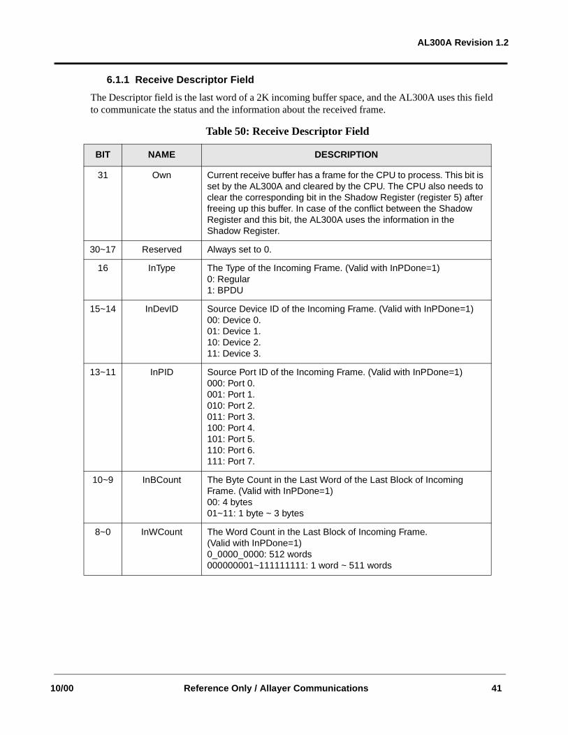
6.1.1 Receive Descriptor Field
The Descriptor field is the last word of a 2K incoming buffer space, and the AL300A uses this field to communicate the status and the information about the received frame.
Table 50: Receive Descriptor Field
BIT NAME DESCRIPTION
31 Own Current receive buffer has a frame for the CPU to process. This bit is set by the AL300A and cleared by the CPU. The CPU also needs to clear the corresponding bit in the Shadow Register (register 5) after freeing up this buffer. In case of the conflict between the Shadow Register and this bit, the AL300A uses the information in the Shadow Register.
30~17 Reserved Always set to 0.
16 InType The Type of the Incoming Frame. (Valid with InPDone=1)0: Regular1: BPDU
15~14 InDevID Source Device ID of the Incoming Frame. (Valid with InPDone=1)00: Device 0.01: Device 1.10: Device 2.11: Device 3.
13~11 InPID Source Port ID of the Incoming Frame. (Valid with InPDone=1)000: Port 0.001: Port 1.010: Port 2.011: Port 3.100: Port 4.101: Port 5.110: Port 6.111: Port 7.
10~9 InBCount The Byte Count in the Last Word of the Last Block of Incoming Frame. (Valid with InPDone=1)00: 4 bytes01~11: 1 byte ~ 3 bytes
8~0 InWCount The Word Count in the Last Block of Incoming Frame. (Valid with InPDone=1)0_0000_0000: 512 words000000001~111111111: 1 word ~ 511 words
10/00 Reference Only / Allayer Communications 41

AL300A Revision 1.2
6.2 Frame Transmission
When data is transferred from the CPU to the network ports, the frame data generated by the CPU will be put into the host memory location allocated by the CPU. The AL300A transfers the outgoing frame through the Transmit DMA Channel onto the RoX Ring which will deliver the frame to the right network port for transmission. The AL300A always generates the FCS field for the frame data, and sends the whole frame through the RoX Ring to its destination port(s). The AL300A does not enforce legal frame length. The CPU supplies the AL300A with the destination port bit map for every frame it generated. The Transmit DMA channel operates as below.
1. The CPU initiates the transmission by writing the frame destination(s) and the frame type (BPDU or regular) data into the AL300A command register. (Issue a command “Outgoing Frame Transfer Notification” which is Command Type 8.) The CPU will then authorize the outgoing frame transfer to the AL300A by writing to the Command Register with the block location in the host memory, and the number of word and byte count which indicates the size of transfer. (Issue a command “Outgoing Frame Transfer DMA Initialization,” Command Type 7.)
2. The DMA engine arbitrates for the bus mastership, and once granted, transfers the frame data from the host memory to the Tx FIFO.
3. After the frame transfer is finished, the DMA engine issues an interrupt (if enabled) notifying the CPU the end of frame transfer from the host memory.
There is no static transmit buffer structure assumed by the AL300A. It is up to the host processes to create and manage as many transmit buffers as needed.
6.3 MAC Address Table Update Access
Whenever the AL300A receives table convergence messages, it stores the changes (using Table Convergence Message format) in a dedicated 8K byte host memory. Each entry takes eight bytes, therefore the buffer stores up to 1K MAC address updates. The AL300A uses 4-bit registers to communicate the status of the Table Convergence Message buffers with the CPU. The AL300A will interrupt after the 2K memory (256 messages) space is full and if the table convergence (register 00, bit 24) is unmasked. The CPU can determine the validity of the message by reading the valid bit of each entry. The 8K bytes of MAC address buffer memory space must be initialized to “0”s upon host initialization.
The host process has the option to either process the message buffer though polling at slow intervals or enable the interrupt and process the MAC address changes in blocks of 256 entries. This 1K MAC address update buffer is not sorted and may contain duplicate MAC addresses. Because this buffer contains MAC address changes, a particular MAC address may age out and be re-learned. It is recommended that a host process and copy the content of the buffer and then sort it based by MAC address, and remove the redundant MAC entries. When handling redundant messages, discard the MAC address that is older, in case the MAC address update occurred as the result of the network node being moved from a port to another port.
Alternatively, an individual MAC address could be read from any of the RoX Bus devices by performing the Indirect Read command through the command register. Each read operation reads in 16-bit data, and requires four indirect read cycles to receive a MAC address. Up to 4096 indirect read command cycles are needed to read the 1K MAC address table from each device. Because the MAC address table is the same among all the devices, only one device needs to read any given RoX
10/00 Reference Only / Allayer Communications 42

AL300A Revision 1.2
Bus system if the table convergence mode is set. The MAC address convergence entry format is as follows:
Table 51: Upper 32-Bit Word Of MAC Address Entry
BIT NAME DESCRIPTION
31~30 Reserved Always set to 0.
29 AV Address Valid. Set by the AL300A and cleared by the CPU.0: Table entry is not valid.1: Table entry is valid.
28 TR Source Port Trunking Mode.0: SrcPID field reflects trunk ID.1: SrcPID field reflects port ID.
27~26 SrcDevID RoX Bus Device ID.00: Device 0.01: Device 1.10: Device 2.11: Device 3.
25~23 SrcPID Source Port ID of the Incoming Frame.000: Port 0.001: Port 1.010: Port 2.011: Port 3.100: Port 4.101: Port 5.110: Port 6.111: Port 7.
22~16 TimeStamp Older Addresses have a Higher Value.
15~0 MACAddr<47:32> Most Significant 16-bit of the MAC Address to be Learned.
Table 52: Lower 32-Bit Word Of MAC Address Entry
BIT NAME DESCRIPTION
31~0 MACAddr<31:0> Least Significant 32-bit of the MAC Address to be Learned.
10/00 Reference Only / Allayer Communications 43

AL300A Revision 1.2
7. Microprocessor Interface Description
7.1 MPC801 Type Interface (P_SEL = 0)
The MPC801 can only access the management functions of the AL300A using single beat read/write cycles. The MPC801 must assert CS# when accessing the AL300A. All burst cycle related signals such as BURST# and BDIP# will be ignored. During the data transfer phase, data is transferred from the MPC801 to the AL300A in write cycles or from the AL300A to the MPC801 on a read cycle. To avoid electrical contention, the MPC801 considers “one dead clock cycle” when switching between drivers. The MPC801 can stop driving the data bus as soon as it samples the TA# signal asserted on the rising edge of the CLKout signal. On a read cycle the MPC801 accepts the data bus contents as valid at the rising edge of the CLKout signal in which the TA# signal is sample asserted.
7.1.1 Read Cycle Timing
The basic read cycle begins with bus arbitration, followed by the address and assertion of TS# (transfer start). After receiving the address, the AL300A returns the data and asserts TA# (transfer acknowledge) and the CPU reads the data. A typical read operation is shown in Figure 7.
10/00 Reference Only / Allayer Communications 44

AL300A Revision 1.2
Figure 7 Single Beat Read Cycle - Zero Wait States Bus
CLKout
BR#
BG#
A[0:31]
RD/WR#
TSIZ[0:1]
BURST#
TS#
DATA
TA#
Data is valid
Receive bus grant and bus busy negated
BB# Assert BB#, Drive address and assert TS#
10/00 Reference Only / Allayer Communications 45

AL300A Revision 1.2
7.1.2 Write Cycle Timing
The basic write cycle begins with bus arbitration, followed by the address, data, and assertion of TS# (transfer start). The AL300A asserts TA# (transfer acknowledge) and samples the data. A single beat write cycle is shown below in Figure 8.
The BDIP# signal is ignored and assumed de-asserted, which means the burst cycles are not supported for direct data transfer between CPU and the AL300A.
Figure 8 Single Beat Write Cycle - Zero Wait States Bus
CLKout
BR#
BG#
A[0:31]
RD/WR#
TSIZ[0:1]
BURST#
TS#
DATA
TA#
Data is sampled
Receive bus grant and bus busynegated
BB# Assert BB#, Drive address and assert TS#
10/00 Reference Only / Allayer Communications 46

AL300A Revision 1.2
7.1.3 AL300A and MPC801 Burst Cycles
The bridging function data transfers are performed by the burst mechanism. When performing the bridging function, the AL300A acts as a DMA master and starts a DMA cycle by asserting the P_BR# (bus request). The AL300A can work with either the MPC801 on chip arbiter or an external arbiter.
After obtaining control of the bus, the AL300A will transfer data to and from memory using burst cycle. The BI# signal to the memory controller must be tied high on the board, therefore any memory attached to the AL300A must be able to support burst cycle. Each burst cycle consists of 16 bus cycles while a wait state can be inserted to slow down the bus cycle. The AL300A transfers data to and from the system memory in a burst of four 32-bit words or 16-bytes. The AL300A will not relinquish control of the bus for another arbitration cycle of four 16-byte bursts (64-byte transfer), or until the data transfer is completed.
The AL300A drives the data during the data phase of a burst write cycle. It also asserts BDIP# signal if it intends to drive the data beat after the current data beat.
Figure 9 Power PC 801 Interface to the AL300A (Block Diagram)
MPC801 AL300A
CS#
PDIP#
BB#
BG#
BR#
TA#
BURST#
TS#
RWC
D[0:31]
A[2:19]
Multiplexer
DRAM
baddr[28:30]
10/00 Reference Only / Allayer Communications 47

AL300A Revision 1.2
Figure 10 Power PC 801 Interface to the AL300A (Timing Diagram)
CLKout
BR#
BG#
A[0:31]
RD/WR#
TSIZ[0:1]
BURST#
TS#
DATA
TA#
BB#
BDIP#
'00'
Last beat
Expects another data
Data is valid
10/00 Reference Only / Allayer Communications 48

AL300A Revision 1.2
The AL300A receives data from the memory during the data phase of a burst read cycle. If the AL300A needs more than one 32-bit word of data, it will assert BDIP# signal when the data is received before the last data. The AL300A de-asserts BDIP# signal and the memory stops driving new data after it receives the negation of the BDIP# signal at the rising edge of the clock. A typical read operation is shown in Figure 11.
Figure 11 Typical Burst Read Cycle for MPC801
CLKout
BR#
BG#
A[0:31]
RD/WR#
TSIZ[0:1]
BURST#
TS#
DATA
TA#
BB#
BDIP#
'00'
Last beat
Will drive another data
Data is sampled
10/00 Reference Only / Allayer Communications 49

AL300A Revision 1.2
7.1.4 Relinquishing the Bus
After transferring a 64-byte burst, P_BR# will be de-asserted for a P_CLK cycle and at the same time, P_BB# will be high. If more data needs to be transferred, P_BR# will be asserted again in the next clock cycle and if bus is granted right-of-way (P_BG# is low from arbiter), P_BB# will be asserted in the next clock cycle. In other words, P_BR# will be high for at least one P_CLK cycle and P_BB# will be high for at least two P_CLK cycles between bursts.
7.2 486 Type Interface (P_SEL = 1)
7.2.1 Read/Write Cycle Timing
A CPU with 486-type bus interface can access the management functions of the AL300A using a single beat read/write cycle. The MPC801 must assert CS# when accessing the AL300A. All burst cycle related signals such as BURST# and BDIP# will be ignored. During the data transfer phase, data is transferred from MPC801 to the AL300A in write cycles or from the AL300A to the MPC801 on read cycle. To avoid electrical contention, the MPC801 considers “one dead clock cycle” when switching between drivers. The MPC801 can stop driving the data bus as soon as it samples the TA# signal asserted on the rising edge of the CLKout signal. On a read cycle the MPC801 accepts the data bus contents as valid at the rising edge of the CLKout signal in which the TA# signal is sample asserted.
A CPU with 486-type bus interface can access the management function of the AL300A using a two-cycle read/write cycles. The CPU must first assert CS# in order to access the AL300A. All burst cycle related signals such as BLAST# and BRDY# will be ignored. The basic two-clock read/write cycles is initiated by the processor with the assertion of the address status signal (ADS#) at the rising edge of the first clock, with the valid bus cycle definition and address. The non-burst ready (RDY#) is asserted by the AL300A in the second clock. The RDY# indicates that the AL300A has presented valid data on the data pins in response to a read request or the AL300A has accepted data in response to a write request.
The CPU samples RDY# at the end of the second clock. The cycle is completed if RDY# is asserted (LOW) when sampled, otherwise a wait state is inserted by AL300A. Note that the RDY# is ignored at the end of the first clock of the bus cycle.
A BLAST# signal is ignored and assumed asserted, which means burst cycles are not supported for direct data transfer between the CPU and the AL300A.
A typical read/write operation is shown in Figure 12.
10/00 Reference Only / Allayer Communications 50

AL300A Revision 1.2
Figure 12 Typical Read/Write Cycle for 486 Interface
7.2.2 Burst Cycle Bus Transfer
DMA data transfers are performed by the burst mechanism when the AL300A acts as a DMA master. During burst cycle, a new data is strobed into the AL300A every clock instead of every other clock as in the non-burst cycle. The AL300A starts a DMA cycle by asserted HOLD.
After obtaining control of the bus, the AL300A will transfer data to and from memory using burst cycle. The burst cycle bus transfer starts with the AL300A asserting a signal (ADS#) and driving out an address in the same manner as non-burst cycle. The AL300A indicates that the cycle is a burst cycle by holding the burst last signal (BLAST#) de-asserted in the second clock of the cycle. The memory controller must assert the burst ready signal (BRDY#) indicating it is willing to do a burst cycle. These signals are in addition to the basic signals of the bus.
Memory attached to the AL300A must be able to support burst cycle. Wait cycles can be inserted to slow down the transfer rate. The AL300A transfers data to and from the system memory in bursts of four 32-bit words or 16 bytes. The AL300A will not relinquish control of the bus for another arbitration cycle for four 16-byte bursts (64-byte transfer), or until the data transfer is completed.
In cases when one 32-bit data transfer takes place, where BLAST# asserts in the second clock-cycle of the transfer cycle, memory controller may assert RDY# instead of BRDY#.
A31-A2MIO#
W/R#
RDY#
DATA
BLAST#
CLKout
ADS#
T1 T2 T1 T2 T1 T2
to CPU from CPU to CPU
Read/ w rite cycleinitiated
Data ready
10/00 Reference Only / Allayer Communications 51

AL300A Revision 1.2
The AL300A will respond to the interrupt acknowledge cycles generated by CPU by providing an interrupt vector. This vector is programmed by writing to the Interrupt Vector Register.
A typical burst read/write operation is shown in Figure 13.
Figure 13 Typical Burst Read/Write Cycle for 486 Bus
7.2.3 Relinquishing the Bus
Since a 486 does not have a P_BB# equivalent signal, the HOLD signal serves the purposes of request and hold. The 486 will grant the bus to the AL300A by asserted HLDA when both signals are active high. Between bursts, the AL300A will de-assert HOLD signal (pull to low) for at least one P_CLK cycle. If more data needs to be transferred, HOLD will be asserted in the next clock cycle.
A31-A4M/IO#
CLKout
ADS#
T1 T2 T2T2 T2 Ti
RD/WR#
RDY#
DATA
BLAST#
to CPU to CPU to CPUto CPU
BRDY#
A3-A2
10/00 Reference Only / Allayer Communications 52

AL300A Revision 1.2
8. Signal Timing Specification
Table 53: CPU Bus Timing
SIGNAL
INPUT OUTPUT
MIN. SETUP MIN. HOLD MIN. DELAY TYP. DELAY MAX. DELAY
P_D 8.0ns 2.5ns 2.0ns 6ns 10.0ns
P_A 8.0ns 2.5ns 2.0ns 6ns 10.0ns
P_BURST 8.0ns 2.5ns 2.0ns 6ns 10.0ns
P_BB 8.0ns 2.5ns 2.0ns 6ns 10.0ns
P_TS 8.0ns 2.5ns 2.0ns 6ns 10.0ns
RWC 8.0ns 2.5ns 2.0ns 6ns 10.0ns
P_TA 8.0ns 2.5ns 2.0ns 6ns 10.0ns
P_INT -- -- 2.0ns 6ns 10.0ns
P_BDIP 8.0ns 2.5ns 2.0ns 6ns 10.0ns
BRDY 8.0ns 2.5ns -- -- --
P_BR -- -- 2.0ns 6ns 10.0ns
P_BG 8.0ns 2.5ns -- -- --
Table 54: RoX Ring Timing
SIGNAL
INPUT OUTPUT
MIN. SETUP MIN. HOLD MIN. DELAY TYP. DELAY MAX. DELAY
ROD -- -- 4.0ns 6ns 10.0ns
RODH -- -- 4.0ns 6ns 10.0ns
ROCTL -- -- 4.0ns 6ns 10.0ns
ROTLH -- -- 4.0ns 6ns 10.0ns
RID 3.0ns 2.0ns -- -- --
RIDH 3.0ns 2.0ns -- -- --
RICTL 3.0ns 2.0ns -- -- --
RICTLH 3.0ns 2.0ns -- -- --
10/00 Reference Only / Allayer Communications 53

AL300A Revision 1.2
Note: (*) riclk/3 = <p_CLK <= min. (50 MHz, riclk)
Table 55: Clock Specifications
CHARACTERISTIC MIN MAX UNIT
RoX ring clock frequency 66 75 MHz
Clock tolerance -- 50 ppm
Duty cycle -- 55/45 %
Maximum CPU frequency (*) -- 40 MHz
Duty cycle -- 55/45 %
10/00 Reference Only / Allayer Communications 54

AL300A Revision 1.2
9. Pin Assignments
PIN # PIN NAME SIGNAL TYPE
1 RICTLH I
2 RICTL0 I
3 RICTL1 I
4 RICTL2 I
5 RICTL3 I
6 RICTL4 I
7 RICTL5 I
8 VCC --
9 GND --
10 RICTL6 I
11 RICTL7 I
12 RIDH I
13 RID0 I
14 RID1 I
15 RID2 I
16 RID3 I
17 VCC --
18 GND --
19 RID4 I
20 RID5 I
21 RID6 I
22 RID7 I
23 RID8 I
24 RID9 I
25 VCC --
26 RICLK I
27 GND --
28 RID10 I
29 RID11 I
30 RID12 I
31 RID13 I
32 RID14 I
33 RID15 I
34 RID16 I
35 VCC --
36 GND --
37 GND --
38 RID17 I
39 RID18 I
40 VCC --
41 RID19 I
42 RID20 I
43 RID21 I
44 RID22 I
45 RID23 I
46 GND --
47 RID24 I
48 RID25 I
49 RID26 I
50 RID27 I
51 RID28 I
52 RID29 I
53 RID30 I
54 RID31 I
55 BURST# I/O
56 BB# I/O
57 TS# I/O
58 RWC I/O
59 TA# I/O
10/00 Reference Only / Allayer Communications 55

AL300A Revision 1.2
60 GND --
61 INT# O
62 VCC --
63 BDIP# TO
64 GND --
65 BR# O
66 CS# I
67 BRDY I
68 BG# I
69 P_MST# O
70 P_A2 I/O
71 GND --
72 P_A3 I/O
73 P_A4 I/O
74 VCC --
75 P_A5 I/O
76 P_A6 I/O
77 VCC --
78 GND --
79 P_A7 I/O
80 GND --
81 P_A8 I/O
82 P_A9 I/O
83 P_A10 I/O
84 VCC --
85 P_A11 I/O
86 P_A12 I/O
87 GND --
88 P_A13 I/O
89 GND --
90 P_A14 I/O
91 P_A15 I/O
92 P_A16 I/O
93 P_A17 I/O
94 GND --
95 P_A18 I/O
96 VCC --
97 P_A19 I/O
98 P_D0 I/O
99 P_D1 I/O
100 GND --
101 P_D2 I/O
102 P_D3 I/O
103 P_D4 I/O
104 P_D5 I/O
105 P_D6 I/O
106 P_D7 I/O
107 P_D8 I/O
108 P_D9 I/O
109 GND --
110 P_D10 I/O
111 P_D11 I/O
112 VCC --
113 P_D12 I/O
114 P_D13 I/O
115 P_D14 I/O
116 GND --
117 P_D15 I/O
118 P_D16 I/O
119 P_D17 I/O
120 P_D18 I/O
121 VCC --
10/00 Reference Only / Allayer Communications 56

AL300A Revision 1.2
122 GND --
123 GND --
124 P_D19 I/O
125 P_D20 I/O
126 P_D21 I/O
127 P_D22 I/O
128 P_D23 I/O
129 VCC --
130 PCLK I
131 GND --
132 P_D24 I/O
133 P_D25 I/O
134 P_D26 I/O
135 P_D27 I/O
136 P_D28 I/O
137 GND --
138 GND --
139 VCC --
140 VCC --
141 P_D29 I/O
142 P_D30 I/O
143 P_D31 I/O
144 P_SEL I
145 P_RST I
146 ROD31 O
147 ROD30 O
148 GND --
149 VCC --
150 ROD29 O
151 ROD28 O
152 ROD27 O
153 GND --
154 ROD26 O
155 ROD25 O
156 ROD24 O
157 ROD23 O
158 ROD22 O
159 ROD21 O
160 ROD20 O
161 ROD19 O
162 GND --
163 ROD18 O
164 ROD17 O
165 ROD16 O
166 VCC --
167 GND --
168 ROD15 O
169 ROD14 O
170 GND --
171 ROD13 O
172 ROD12 O
173 ROD11 O
174 ROD10 O
175 ROD9 O
176 GND --
177 ROD8 O
178 ROD7 O
179 VCC --
180 ROD6 O
181 ROD5 O
182 VCC --
183 GND --
10/00 Reference Only / Allayer Communications 57
AL300A Revision 1.2
184 ROD4 O
185 GND --
186 ROD3 O
187 VCC --
188 ROD2 O
189 ROD1 O
190 ROD0 O
191 RODH O
192 GND --
193 ROCTL7 O
194 ROCTL6 O
195 GND --
196 ROCTL5 O
197 ROCTL4 O
198 ROCTL3 O
199 VCC --
200 GND --
201 ROCTL2 O
202 ROCTL1 O
203 ROCTL0 O
204 ROCTLH O
205 TEST0 I/O
206 TEST1 O
207 TEST2 O
208 TEST3 O
10/00 Reference Only / Allayer Communications 58
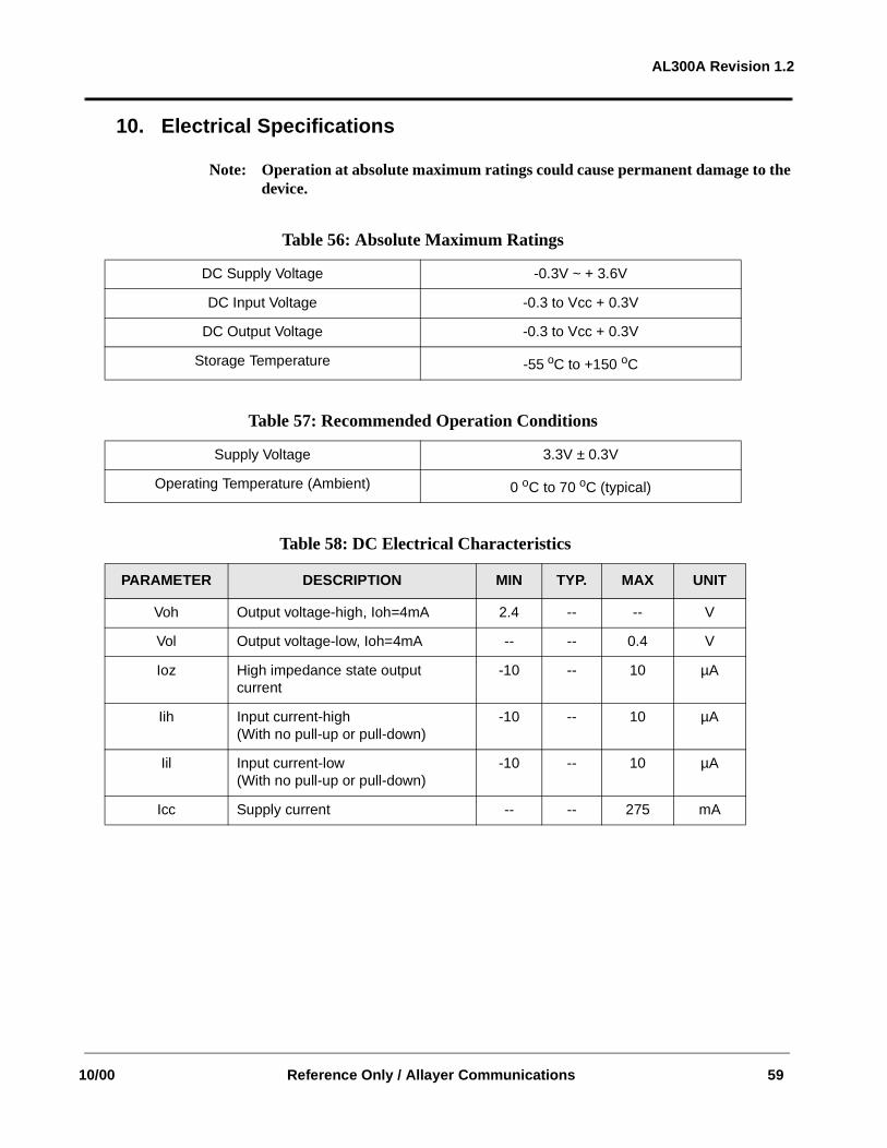
AL300A Revision 1.2
10. Electrical Specifications
Note: Operation at absolute maximum ratings could cause permanent damage to the device.
Table 56: Absolute Maximum Ratings
DC Supply Voltage -0.3V ~ + 3.6V
DC Input Voltage -0.3 to Vcc + 0.3V
DC Output Voltage -0.3 to Vcc + 0.3V
Storage Temperature -55 oC to +150 oC
Table 57: Recommended Operation Conditions
Supply Voltage 3.3V ± 0.3V
Operating Temperature (Ambient) 0 oC to 70 oC (typical)
Table 58: DC Electrical Characteristics
PARAMETER DESCRIPTION MIN TYP. MAX UNIT
Voh Output voltage-high, Ioh=4mA 2.4 -- -- V
Vol Output voltage-low, Ioh=4mA -- -- 0.4 V
Ioz High impedance state output current
-10 -- 10 µA
Iih Input current-high (With no pull-up or pull-down)
-10 -- 10 µA
Iil Input current-low(With no pull-up or pull-down)
-10 -- 10 µA
Icc Supply current -- -- 275 mA
10/00 Reference Only / Allayer Communications 59

AL300A Revision 1.2
11. AL300A Mechanical Data
208-Pin PQFP Package
Figure 14 AL300A Mechanical Dimensions
0.20 ± 0.05
0.50 ± 0.01
28.00 ± 0.13
30.6 ± 0.3
0.10 min.
3.68 max.
1.30 ± 0.20
0.50 ± 0.20 0.10 min.
3.23 ± 0.12
25.5 mm
10/00 Reference Only / Allayer Communications 60

AL300A Revision 1.2
Rev. History
Prelim. 1.2 to 1.2a
1. Reformatted and edited document.
2. Changed pin 84 from ground to VCC.
Prelim 1.2a to 1.3
1. Updated electrical specifications.
2. Corrected mechanical diagram dimensions.
Prelim. 1.3 to Rev. 1.0
1. Fully released document.
Rev. 1.0 to 1.1
1. Changed reference to InPReady to InPDone.
2. Corrected RD/WR# line in figure 13.
Rev. 1.1 to 1.2
1. Updated the MIB statistics collection description in section 3.6.
10/00 Reference Only / Allayer Communications 61

Index
Numerics1 Gbit/s MIB Register Descriptions 35100Mbit/s MIB Register Descriptions 32100Mbit/s MIB Registers In AL300A 31208 Pin PQFP Package 6486 Type Interface (P_SEL = 1) 50
AAbsolute Maximum Ratings 59Access AL1022 Port MIB Information 27AL300A and MPC801 Burst Cycles 47AL300A Functional Block Diagram 9AL300A Host Memory Requirements for the DMA Access 12AL300A Overview 5AL300A Pin Diagram 6
BBurst Cycle Bus Transfer 51
CClear AL300A Port MIB Information 27Clock Specifications 54Configuration Register I (Register 00) 18Configuration Register II (Register 01) 19CPU Bus Timing 53CPU Processor Interface 7
DDC Electrical Characteristics 59
FFrame Reception 39Frame Transmission 42Functional Description 9
HHost In Register I (Register 0B) 30Host In Register II (Register 0C) 30Host Memory MIB Structure 37Host MIB Count Hold 24Host MIB Count Unhold 24Host Out Register I (Register 08) 29Host Out Register II (Register 09) 29Host Out Register III (Register 0A) 29
IIndirect Access Read 22Indirect Access Write 22Interrupt Mechanism 13Interrupt Vector Register (Intel Mode Only)(Register 06) 29
LLower 32-Bit Word Of MAC Address Entry 43
MMAC Address Table Update Access 42MAC Services 11
Host Frame Transmission and Reception 39Managed Switch Using RoX Bus 10Matrix Register I (Register 0D) 30
Matrix Register II (Register 0E) 30MIB Counters Mechanism 37MIB Registers 31MIB Statistics Collection 14Microprocessor Interface and MAC Services 11Microprocessor Interface Description 44MPC801 Type Interface (P_SEL = 0) 44
PPin Descriptions 7Port Related Etherstat MIB Access 14Power And Miscellaneous I/O 8Power PC 801 Interface to the AL300A (Block Diagram) 47Power PC 801 Interface to the AL300A (Timing Diagram) 48Product Description 1
RRead AL300A Port MIB Information 26Read/Write Cycle Timing 50Reading MIB Counters Mechanism 37Receive Descriptor Field 41Receive Frame Buffer DMA Initialization 25Recommended Operation Conditions 59Register 04
Indirect Access Result Register 28Register Descriptions 15Register Structure of AL300A 16Relinquishing the Bus 50, 52RMON Host Group MIB Access 15RoX Bus Description 10RoX Input Interface 8RoX Output Interface 8RoX Ring Timing 53
SSet Table Convergence Base Address 23Shadow Register for Receive Buffer Ownership (Register 05) 28Signal Timing Specification 53Single Beat Read Cycle - Zero Wait States Bus 45Single Beat Write Cycle - Zero Wait States Bus 46Spanning Tree Support 13Switch Management Engine 1System Block Diagram 1System Status and Configuration 13
TTest Pin 8Test Register (Register 07) 29Transmit Frame DMA Initialization 25Transmit Frame Transfer Notification 26Types of CPU Interface 11Typical Burst Read Cycle for MPC801 49Typical Read/Write Cycle for 486 Interface 51
UUpper 32-Bit Word Of MAC Address Entry 43
Reference Only / Allayer Communications


![Little Rox Stories [lq]](https://static.fdocuments.net/doc/165x107/568bd83c1a28ab2034a29f1e/little-rox-stories-lq.jpg)