Advanced Photoemission Spectroscopy Investigations ...
10
Advanced Photoemission Spectroscopy Investigations Correlated with DFT Calculations on the Self-Assembly of 2D Metal Organic Frameworks Nano Thin Films Radwan Elzein, † Chun-Min Chang, ‡,§ Inna Ponomareva, ‡ Wen-Yang Gao, ∥ Shengqian Ma, ∥ and Rudy Schlaf* ,† † Department of Electrical Engineering, University of South Florida, Tampa, Florida 33620, United States ‡ Department of Physics, University of South Florida, Tampa, Florida 33620, United States § Institute for Cyber-Enabled Research, Michigan State University, East Lansing, Michigan 48824, United States ∥ Department of Chemistry, University of South Florida, Tampa, Florida 33620, United States ABSTRACT: Metal−organic frameworks (MOFs) deposited from solution have the potential to form 2-dimensional supra- molecular thin films suitable for molecular electronic applications. However, the main challenges lie in achieving selective attachment to the substrate surface, and the integration of organic conductive ligands into the MOF structure to achieve conductivity. The presented results demonstrate that photoemission spectroscopy combined with preparation in a system- attached glovebox can be used to characterize the electronic structure of such systems. The presented results demonstrate that porphyrin-based 2D MOF structures can be produced and that they exhibit similar electronic structure to that of corresponding conventional porphyrin thin films. Porphyrin MOF multilayer thin films were grown on Au substrates prefunctionalized with 4-mercaptopyridine (MP) via incubation in a glovebox, which was connected to an ultrahigh vacuum system outfitted with photoelectron spectroscopy. The thin film growth process was carried out in several sequential steps. In between individual steps the surface was characterized by photoemission spectroscopy to determine the valence bands and evaluate the growth mode of the film. A comprehensive evaluation of X-ray photoemission spectroscopy (XPS), ultraviolet photoelectron spectroscopy (UPS), and inverse photoemission spectroscopy (IPES) data was performed and correlated with density functional theory (DFT) calculations of the density of states (DOS) of the films involved to yield the molecular-level insights into the growth and the electronic properties of MOF-based 2D thin films. KEYWORDS: metal−organic frameworks, supramolecular self-assembly, 2D thin films, surface science, density of states, DFT calculations, photoemission spectroscopy ■ INTRODUCTION The past two decades have witnessed a growing interest in the area of metal−organic frameworks (MOFs), an advanced class of functional porous materials that adopts concepts from crystal engineering to self-assembled highly ordered crystalline porous materials. 1 MOFs are highly attractive to both academic and industrial communities due to their potential applications in heterogeneous catalysis, 2 gas storage, 3 gas separation, 4 drug delivery, 5 sensing, 6 or storage devices. 7 As crystalline porous coordination polymers, MOFs are constructed by connecting Received: August 17, 2016 Accepted: October 21, 2016 Published: October 21, 2016 Research Article www.acsami.org © 2016 American Chemical Society 31403 DOI: 10.1021/acsami.6b10340 ACS Appl. Mater. Interfaces 2016, 8, 31403−31412
Transcript of Advanced Photoemission Spectroscopy Investigations ...
Advanced Photoemission Spectroscopy Investigations Correlatedwith DFT Calculations on the Self-Assembly of 2D Metal OrganicFrameworks Nano Thin FilmsRadwan Elzein,† Chun-Min Chang,‡,§ Inna Ponomareva,‡ Wen-Yang Gao,∥ Shengqian Ma,∥ andRudy Schlaf*,†
†Department of Electrical Engineering, University of South Florida, Tampa, Florida 33620, United States‡Department of Physics, University of South Florida, Tampa, Florida 33620, United States§Institute for Cyber-Enabled Research, Michigan State University, East Lansing, Michigan 48824, United States∥Department of Chemistry, University of South Florida, Tampa, Florida 33620, United States
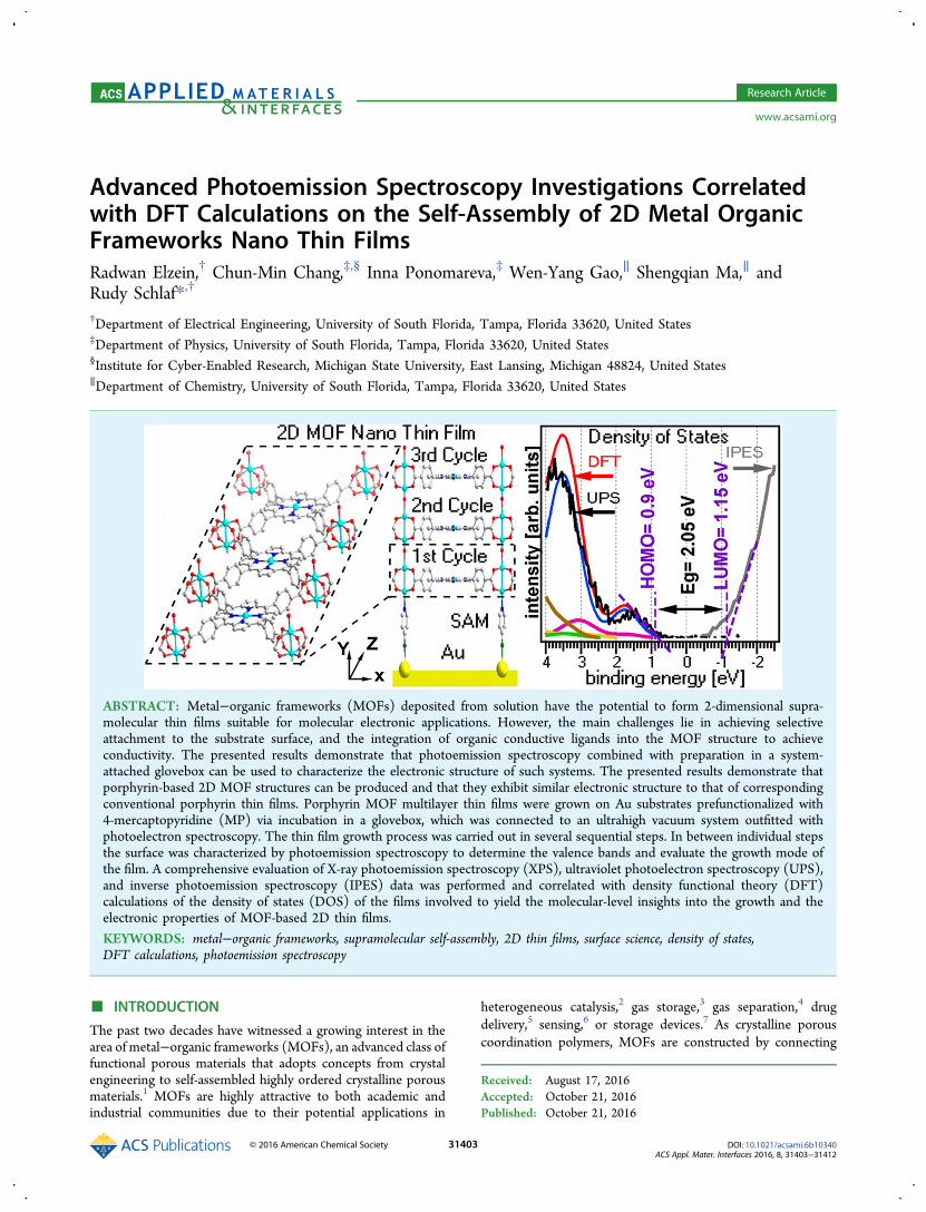
ABSTRACT: Metal−organic frameworks (MOFs) deposited from solution have the potential to form 2-dimensional supra-molecular thin films suitable for molecular electronic applications. However, the main challenges lie in achieving selectiveattachment to the substrate surface, and the integration of organic conductive ligands into the MOF structure to achieveconductivity. The presented results demonstrate that photoemission spectroscopy combined with preparation in a system-attached glovebox can be used to characterize the electronic structure of such systems. The presented results demonstrate thatporphyrin-based 2D MOF structures can be produced and that they exhibit similar electronic structure to that of correspondingconventional porphyrin thin films. Porphyrin MOF multilayer thin films were grown on Au substrates prefunctionalized with4-mercaptopyridine (MP) via incubation in a glovebox, which was connected to an ultrahigh vacuum system outfitted withphotoelectron spectroscopy. The thin film growth process was carried out in several sequential steps. In between individual stepsthe surface was characterized by photoemission spectroscopy to determine the valence bands and evaluate the growth mode ofthe film. A comprehensive evaluation of X-ray photoemission spectroscopy (XPS), ultraviolet photoelectron spectroscopy (UPS),and inverse photoemission spectroscopy (IPES) data was performed and correlated with density functional theory (DFT)calculations of the density of states (DOS) of the films involved to yield the molecular-level insights into the growth and theelectronic properties of MOF-based 2D thin films.
KEYWORDS: metal−organic frameworks, supramolecular self-assembly, 2D thin films, surface science, density of states,DFT calculations, photoemission spectroscopy
■ INTRODUCTION
The past two decades have witnessed a growing interest in thearea of metal−organic frameworks (MOFs), an advanced class offunctional porous materials that adopts concepts from crystalengineering to self-assembled highly ordered crystalline porousmaterials.1 MOFs are highly attractive to both academic andindustrial communities due to their potential applications in
heterogeneous catalysis,2 gas storage,3 gas separation,4 drugdelivery,5 sensing,6 or storage devices.7 As crystalline porouscoordination polymers, MOFs are constructed by connecting
Received: August 17, 2016Accepted: October 21, 2016Published: October 21, 2016
Research Article
www.acsami.org
© 2016 American Chemical Society 31403 DOI: 10.1021/acsami.6b10340ACS Appl. Mater. Interfaces 2016, 8, 31403−31412
metal ions or clusters with organic based ligands. This results inporous crystalline nanoscale frameworks composed of a varietyof molecular compounds containing highly tunable empty spacefor guest molecule adsorption. Meanwhile, this also makes thesematerials interesting for controlled mass transfer and opens upthe prospect of creating tailor designed materials with bothelectronic and ionic conductivity.In particular, the self-assembly of conductive MOF struc-
tures on wafer-type supports and the investigation of theirperformance in device structures are of great interest fornext-generation electronic device development. Such devicescan be manufactured through a combination of standard litho-graphic techniques and molecular self-assembly of embed-ded MOF structures. The resultant materials integrating ionicand electronic conductivity in one single structure wouldexhibit promising applications in energy storage, fuel cells,and other areas. Probably the prime examples are memristive8,7
circuit elements as demonstrated by Hewlett-Packard,9 whichdemonstrate the high significance of materials with combinedelectronic and ionic conductivity for future technological appli-cations. Memristors enable a remarkably simple (comparedto transistor/capacitor based classic static or dynamic ran-dom access memory(RAM)) design of memory elements,which only need two terminals for read and write operations,while being able to store the information for long timeswithout power.The well-developed crystal engineering strategy enables us to
custom design MOFs structures via the judicious selection ofthe metal ions and organic linkers, which also suggests theself-assembly of MOF-based device structures with electronicconductivity is viable. Among a variety of organic linkers used tofabricate nano thin films, porphyrin ligand, because of theirversatility and functionality, present tremendous potential whencombined with suitably chosen active SBUs. However, whenapplying MOF or related coordination materials on nano-electronic devices, the main challenges to be addressed lie incontrolling the size of objects at the nanoscale and aligning suchobjects on surface of various substances in certain desired wayswithout losing their original electronic properties.In essence, π-stacked conjugated molecular structures need
to be achieved in such materials. This was shown recently byNarayan et al.10 who synthesized a conducting porous frameworkbased on columnar stacks of TTFTB (tetrathiafulvalene tetra-benzoate). Recent research on covalent organic frameworks(COFs) has shown that conductive molecular materials likeporphyrins and phthalocyanines can be used for the formationof porous structures with charge transport capabilities.11,12
This suggests that these molecular building blocks should beemployable for conductive MOF structures.The tailor design of conductive MOF structures makes it
necessary that the electronic structure can be measured toprovide feedback for the design process. The presented researchdemonstrates that photoemission spectroscopy in combinationwith clean structural synthesis in a vacuum system attachedglovebox can be used for the characterization of the frontierorbital structure of self-assembled MOF films. This research isbased on an established track record of this measurementtechnique for the characterization of the electronic structure ofinterfaces composed of conductive small molecular as well aspolymeric materials.In essence, the photoemission spectroscopy results of both
UPS and IPES measurements yield the density of states ofthe highest occupied molecular orbitals (HOMO), and lowest
unoccupied molecular orbitals (LUMO), respectively, relative tothe Fermi level. Since this measurement occurs in ultrahighvacuum and also is very surface sensitive (only the top 5 nm are“seen”) the investigated samples need to be prepared in vacuumor in the inert environment of a vacuum-attached glovebox. Suchmeasurements were successfully demonstrated in the past for avariety of molecular materials such as conductive polymers, smallmolecular electroluminescent materials, self-assembled mono-layers, or ribonucleic acids.In this work, the application of this technique to self-assembled
conductive MOF structures is demonstrated. Self-assembledMOF thin films were grown in several steps, while characterizingthe electronic structure depending on the layer thickness. Inthese experiments, MOF thin films composed of TCPP linkersand dicopper paddlewheel secondary building blocks (SBU)were self-assembled on top of SAM-terminated (MP) Au sub-strates. The TCPP molecule is a prototypical linker-moleculecandidate for conductive MOF structures, and well-suited forthe presented measurements since similar measurements werealready demonstrated successfully on evaporated porphyrin thinfilms.13−17 The molecule MP was chosen as SAM substrate forthe structure since it is capable of coordinating to the copperpaddlewheels from axial positions while facilitating charge trans-port. These experiments were accompanied by computationalDFT calculations on the DOS of the prepared MOF structures.These calculations showed strong agreement and allowed theinterpretation of the photoemission data.
■ EXPERIMENTAL SECTIONMaterials: MOFMaterials:MOF Synthesis.Cu(NO3)2 and TCPP
(5,10,15,20-tetrakis(4-carboxyphenyl) porphyrin); 4-mercaptopyridine(96%), as well as anhydrous ethanol were purchased from FisherScientific. The N,N-dimethylformamide (DMF), (ACS, 99.8+%) wasobtained from Alfa Aesar, and the thin film Au (100 nmAu deposited ona 20 nm Ti adhesion layer on glass slides) substrates were purchasedfrom EMF Corp. (Ithaca, NY).
Sample Preparation. All experiments were performed in a com-mercial multichamber system (SPECS Nano Analysis GmbH, Berlin,Germany) under ultrahigh vacuum (UHV) conditions (2 × 10⁻¹⁰ mbarbase pressure). The system consists of a fast entry lock, transfer chamberfor sputtering, and analysis chambers equipped with X-ray, ultraviolet,and inverse photoemission spectroscopy (XPS, UPS, and IPES,respectively). A homemade acrylic glovebox was attached to the loadlock to enable a direct transfer of the sample from the sample prepara-tion area into the vacuum. The glovebox was filled with 99.995%N2 andkept under slight overpressure to suppress sample contamination fromthe ambient environment during sample preparation.
The thin film Au (100 nm thick) substrates were cut into 1 × 1 cm2
pieces and mounted on a substrate holder via screws. This allowed fordirect electrical contact between the Au layer and the chamber groundto avoid charging effects. The substrates were then transferred intoan UHV chamber for sputtering to clean the Au surface. A SPECS IQE11/35 ion source with a kinetic energy of 5 keV and an emission currentof 20 mA was used, and the sample sputtered for 40 min at an Ar pres-sure of 4 mbar.18
After sputtering, the clean Au substrates were characterized by thestandard measurement sequence beginning with an LIXPS measure-ment (Mg K, 1253.6 eV, standby mode: 0.1 mA emission current), thenfollowed by UPS (He I, 21.2182 eV), XPS (Mg K, 1253.6 eV, 20 mAemission current), and finally an IPES measurement (electron gun,Kimball ELG-2/EGPS-1022, and a Geiger counter with an energyresolution of about 0.43 eV).
The deposition experiments started by loading an Au substrate intothe glovebox for the growth of the SAM via incubation. The sample wasplaced into the bottom of a vial containing the SAM solution (1 mMSAM solution of 4-mecaptopyridine in ethanol stirred at 80 °C for 24 h).
ACS Applied Materials & Interfaces Research Article
DOI: 10.1021/acsami.6b10340ACS Appl. Mater. Interfaces 2016, 8, 31403−31412
31404

The vial was sealed and placed in the glovebox for 24 h at 40 °C.After cooling the sample to room temperature, it was removed and thenrinsed gently with ethanol, deionized water, and dried with a stream of99.995% N2.In the first MOF experiment (A), the Au functionalized substrate
was alternately immersed into the metal ion solution (13.329 mMCu(NO3)2 solution in DMF stirred on a hot plate at 80 °C for 24 h) for12 h followed by an immersion step in the organic ligand solution(1.2645 mM TCPP solution in DMF stirred on a hot plate at 80 °C for24 h) for an additional 12 h, three sequential incubation cycles wereperformed in the glovebox at a temperature of 40 °C. In between eachimmersion step, the substrate was rinsed with fresh DMF and deionizedwater to remove excessive unbound molecules from the surface,19 anddried in a stream of 99.995% N2 as depicted in (Schematic 1), whichshows the expected crystal structure.20 Following each individual immer-sion cycle, the surface was characterized with the above LIXPS/UPS/XPSsequence.In a control experiment (B), fresh TCPP and Cu(NO3)2 solutions
were mixed together in a vial following the same concentrations andconditions reported in the main experiment (A). An identical Aufunctionalized surface was immersed into a vial containing the mixedsolution for three incubation cycles in the glovebox each for 24 h at40 °C (identical conditions as in experiment A). After each completeincubation cycle, the substrate was rinsed with DMF and deionizedwater, and then dried with 99.995% N2. This was followed by transferinto the attached vacuum system and PES characterization.
In the second control experiment (C), the Au functionalized surfacewas immersed in the TCCP solution (same concentration and experi-mental conditions as were used in experiment (A)), but the immersionin the Cu(NO3)2 solution was omitted. After the experiment, the samplewas inserted into the vacuum system and then characterized by PES.
Computational Method for DFT Calculations on theElectronic Structure. The molecular modeling software Gaussian09was used to perform all-electron DFT calculations on the metalatedand free base TCPP molecules connected to copper paddle wheels.20
The computed structure of TCPP can be seen from Figure 1a and that ofCuTCPP is shown in Figure 1b.
The Gaussian basis set 6-311G** and DFT exchange correlationfunctional B3LYPwith 2-dimensional periodic boundary condition wereemployed. The ground-state geometries of both MOF structures werefully optimized in vacuum, then the electronic structure and the energylevels were calculated. By considering possible deformation and ther-mal effects in the system, the theoretical DOS spectra are plotted byGaussian broadening of the intensity around each energy eigenvalue.The results are compared with experimental UV photoelectron spectrain the Discussion section.
■ RESULTS
The standard LIXPS-UPS-XPS measurement sequence wascarried out after each sample preparation step. Figure 2 shows theevolution of the C 1s, N 1s, O 1s, S 2p, Cu 2p, and Au 4f core levelemission lines throughout the three experiments A, B, and C.
Scheme 1. Schematic Depiction of the Growth Sequence: MOF Films Were Grown in Three Incubation Cycles on a MPSAM-Terminated Gold Substratea
aFirst, the sample was incubated in the metal ion solution (Cu(NO3)2), followed by immersion into the organic ligand solution (TCPP).Each incubation step was completed by rinsing the sample in DMF and deionized water. Color assignment: carbon, gray; oxygen, red; sulfur, green;nitrogen, blue; and copper, cyan.
Figure 1. Computed structures of MOF molecules connected to Cu paddle wheels. (a) Free base TCPP and (b) metalated CuTCPP.
ACS Applied Materials & Interfaces Research Article
DOI: 10.1021/acsami.6b10340ACS Appl. Mater. Interfaces 2016, 8, 31403−31412
31405
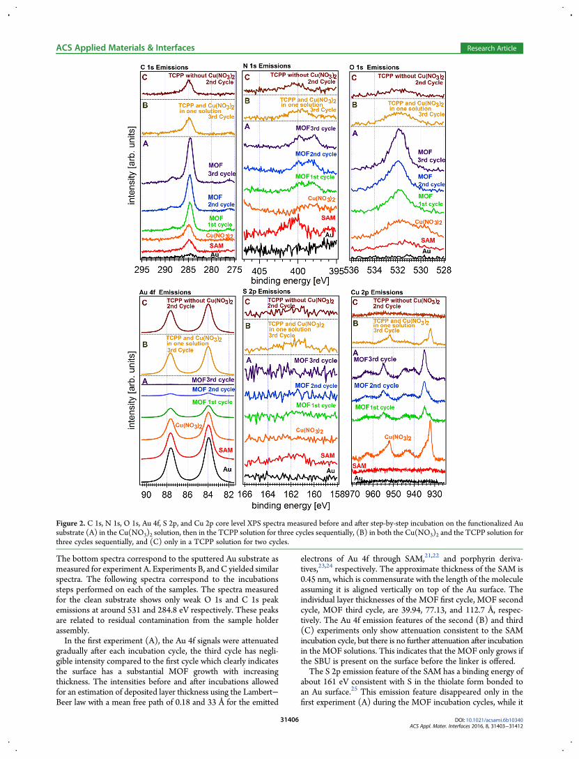
The bottom spectra correspond to the sputtered Au substrate asmeasured for experiment A. Experiments B, and C yielded similarspectra. The following spectra correspond to the incubationssteps performed on each of the samples. The spectra measuredfor the clean substrate shows only weak O 1s and C 1s peakemissions at around 531 and 284.8 eV respectively. These peaksare related to residual contamination from the sample holderassembly.In the first experiment (A), the Au 4f signals were attenuated
gradually after each incubation cycle, the third cycle has negli-gible intensity compared to the first cycle which clearly indicatesthe surface has a substantial MOF growth with increasingthickness. The intensities before and after incubations allowedfor an estimation of deposited layer thickness using the Lambert−Beer law with a mean free path of 0.18 and 33 Å for the emitted
electrons of Au 4f through SAM,21,22 and porphyrin deriva-tives,23,24 respectively. The approximate thickness of the SAM is0.45 nm, which is commensurate with the length of the moleculeassuming it is aligned vertically on top of the Au surface. Theindividual layer thicknesses of the MOF first cycle, MOF secondcycle, MOF third cycle, are 39.94, 77.13, and 112.7 Å, respec-tively. The Au 4f emission features of the second (B) and third(C) experiments only show attenuation consistent to the SAMincubation cycle, but there is no further attenuation after incubationin the MOF solutions. This indicates that the MOF only grows ifthe SBU is present on the surface before the linker is offered.The S 2p emission feature of the SAM has a binding energy of
about 161 eV consistent with S in the thiolate form bonded toan Au surface.25 This emission feature disappeared only in thefirst experiment (A) during the MOF incubation cycles, while it
Figure 2. C 1s, N 1s, O 1s, Au 4f, S 2p, and Cu 2p core level XPS spectra measured before and after step-by-step incubation on the functionalized Ausubstrate (A) in the Cu(NO3)2 solution, then in the TCPP solution for three cycles sequentially, (B) in both the Cu(NO3)2 and the TCPP solution forthree cycles sequentially, and (C) only in a TCPP solution for two cycles.
ACS Applied Materials & Interfaces Research Article
DOI: 10.1021/acsami.6b10340ACS Appl. Mater. Interfaces 2016, 8, 31403−31412
31406
remained unchanged in the control experiments. This furthersupports the conclusion that the MOF film only grows if Cu(NO3)2 was deposited prior to incubation in TCPP. A similarbehavior is seen in all other MOF overlayer related emissions.MOF-related emissions occur only in experiment A, while experi-ments B and C do not show much change after the SAM hasgrown.The aromatic hydrocarbon related C 1s emission features
of both SAM and TCPP multilayers produce a peak at about285 eV. The distinguishing element in the C 1s spectra of theMOF layer has a smaller emission at about 288 eV, which isrelated to CO bonds, which are found in the COOH groups ofthe MOF.26,27 This feature only occurs in experiment (A), whilethe emissions seen in (B) and (C) retain their shape, intensity,and binding energy during the incubation steps. This supportthat no film grew on top of the SAM layer.The O 1s emission featured shows a similar behavior. There is
a small O 1s emission feature present after the SAM growth step.This emission line is related to the residual surface contaminationof surrounding areas on the substrate holder.28 In experiment(A), this emission is attenuated at the expense of a strongnew peak that is related to the COOH groups present in theMOF film.29 Control experiment (B) shows a change in the O 1sspectrum due a small amount of deposited Cu(NO3)2 indicatingthat some molecules deposited on the surface during theincubation step. Experiment (C) shows again no change relativeto the initial SAM layer, indicating that no film deposition. Thisclearly shows that Cu (NO3)2 needs to be present on the surfacebefore incubation in TCPP if a thin film is to be grown.The Cu 2p emission from the Cu(NO3)2 (orange spectrum)
shows only contributions of Cu(I) with a binding energy of932.4 eV. However, once the TCPP was added onto thesurface, the Cu 2p emission (purple spectrum) revealed Cu(II)characteristic at 936.1 eV and additional satellite peaks at940 and 944.3 eV assuming a Cu paddle wheel SBU wasassembled by self-organization in situ by the presence of TCPP.This is also supported by the particular structure of the observedemissions, which agree well with the data published by othergroups.30,31 In addition, the binding energy of the spectrachanges significantly once the MOF film forms. This is seen inthe sequence of spectra of experiment (A) as the MOF filmgrows in thickness. The initial spectrum measured after theCu(NO3)2 deposition step is gradually attenuated, while aspectrum with peaks shifted by about 3 eV to higher bindingenergy arises. This indicates a charge transfer from theCu(NO3)2 building blocks to the TCPP spacers as the MOFforms.The analysis of theN 1s spectra sequence is consistent with the
Cu 2p series. The initial N 1s spectrum (red) of the SAM shows abroad peak at about 400.1 eV, which confirms the deposition ofMP on the Au surface. The N 1s spectra measured during thegrowth of the MOF film (green spectrum) during experiment(A) exhibit distinctly different emission features that are attri-buted to a molecule containing pyrolic (NH) and iminic(N) nitrogen species. These are strong indicators that aninteraction between Cu atoms and TCPP molecules took place.These emission lines are located at 397.9 and 399.8 eV, respec-tively, which are in close agreement with other experimentsfound in the literature.32−40
The shift of Cu 2p to higher binding energies and the N 1s tolower binding energies indicate that electrons were donated fromthe copper atoms to the TCPPmolecules, as electron loss usuallyresults in higher binding energies.18
In summary, the XPS data clearly show that a layered self-assembly process of an MOF structure occurs between theCu(NO3)2 and TCPP molecular units when Cu(NO3)2 isdeposited on the surface before the TCPP incubation steps.When Cu(NO3)2 and TCPP are directly mixed in solution,this process does not occur, possibly due to the formation of3D MOF structures in solution which do not deposit on thepresented SAM surfaces.
UPS and LIXPS Measurements. Prior to each XPSmeasurement sequence, the samples were characterized withUPS and LIXPS. LIXPS uses the XPS, an X-ray gun in its standbysetting, i.e., uses a very low photon density. This low densityis still enough to perform a successful measurement of thesecondary edge, i.e., the work function can be detected. Thisapproach allows the detection of charging artifacts that oftenoccur during UPS measurements due to the relatively highphoton density of UV sources. Especially on organic materialsthis can be an issue due to the often low conductivity of thesematerials, which prevents the effective replenishment of photoextracted electrons. This causes charging, which manifestsitself in peak shifts. LIXPS is much less affected by chargingphenomena, i.e., comparing UPS, and LIXPS work functionmeasurements reveal the onset of charging artifacts in UPS mea-surements.41,42
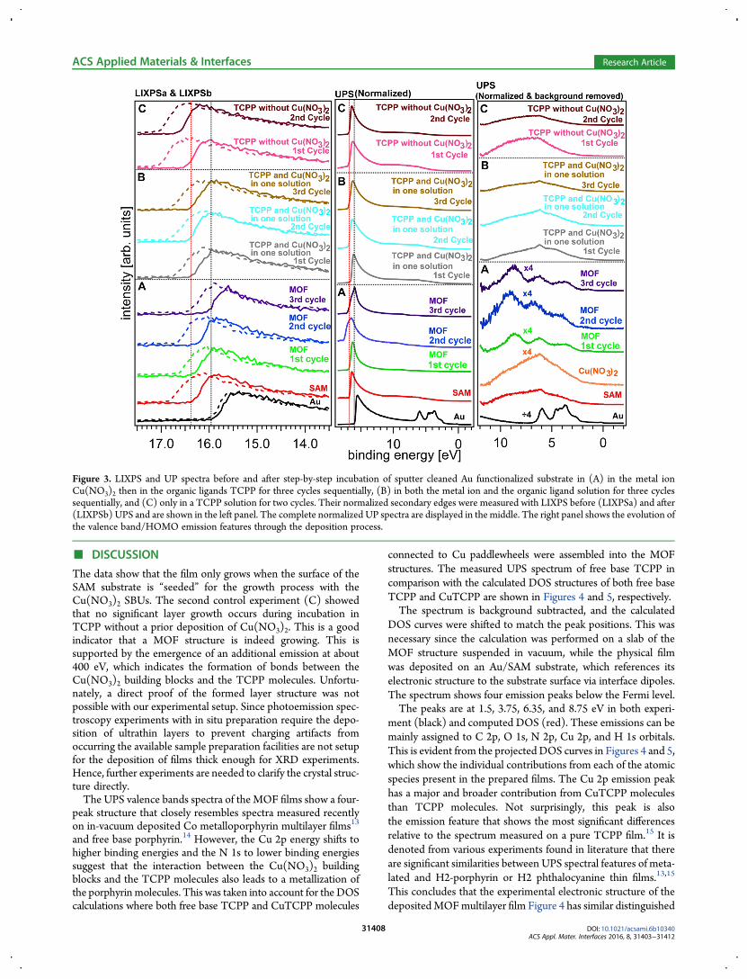
The UP- and LIXP-spectra measured in conjunction with theXPS spectra of Figure 2 are shown in Figure 3. The center graphshows the full UP-spectra measured after each experimental step.The left graph shows the corresponding LIXPSa and LIXPSb(dashed lines) spectra as measured before and after the UPSmeasurements, respectively. The right part shows the valencebands/HOMO regions of the spectra. 0 eV represents the Fermienergy.The secondary edge feature of the LIXP-spectra, located
between 16 and 18 eV, is defined by the work function of thesample (Figure 3, left panel). Each incubation cycle producedintense spectral lines corresponding to the frontier orbital statesof the deposited molecules, while strongly attenuating the Auemissions. The secondary cutoff shifted to higher binding energyafter each of the incubations, indicating a decrease in the Ausurface work function due to the interaction between the surfaceand the MOF film. The work functions were determined aftereach incubation step bymeasuring the high binding energy cutoffat the secondary edge where the spectra ends are located. Thisvalue is 15.9752 eV in case for Au. Hence, the work function canbe determined by the difference between the energy of the UVphotons (21.2182 eV for He I excitation energy) and the Au bind-ing energy (black spectrum) of the secondary edge 15.9752 eV,and by adding the analyzer broadening (analyzer correction factor)of approximately 0.1 eV. Similarly, the work functions of theSAM and MOF, 4.3 and 5.16 eV, respectively, were determinedfrom the LIXPS measurements rather than the UPS measure-ments to avoid any charging artifacts or photochemical surfacemodifications that can occur during the UPS measurement.The valence bands and the HOMO regions after background
subtraction are shown in Figure 3, right panel, the bottom(black) spectrum shows the typical emissions for a clean Ausurface after in situ sputtering. After step-by-step incubationsof the metal ions and the organic ligands, the Au features areattenuated and replaced by emissions related to the valencebands/HOMO levels of the SAM film (red spectrum) and theMOF film (green, blue, and purple spectra).
ACS Applied Materials & Interfaces Research Article
DOI: 10.1021/acsami.6b10340ACS Appl. Mater. Interfaces 2016, 8, 31403−31412
31407
■ DISCUSSION
The data show that the film only grows when the surface of theSAM substrate is “seeded” for the growth process with theCu(NO3)2 SBUs. The second control experiment (C) showedthat no significant layer growth occurs during incubation inTCPP without a prior deposition of Cu(NO3)2. This is a goodindicator that a MOF structure is indeed growing. This issupported by the emergence of an additional emission at about400 eV, which indicates the formation of bonds between theCu(NO3)2 building blocks and the TCPP molecules. Unfortu-nately, a direct proof of the formed layer structure was notpossible with our experimental setup. Since photoemission spec-troscopy experiments with in situ preparation require the depo-sition of ultrathin layers to prevent charging artifacts fromoccurring the available sample preparation facilities are not setupfor the deposition of films thick enough for XRD experiments.Hence, further experiments are needed to clarify the crystal struc-ture directly.The UPS valence bands spectra of the MOF films show a four-
peak structure that closely resembles spectra measured recentlyon in-vacuum deposited Co metalloporphyrin multilayer films13
and free base porphyrin.14 However, the Cu 2p energy shifts tohigher binding energies and the N 1s to lower binding energiessuggest that the interaction between the Cu(NO3)2 buildingblocks and the TCPP molecules also leads to a metallization ofthe porphyrin molecules. This was taken into account for the DOScalculations where both free base TCPP and CuTCPP molecules
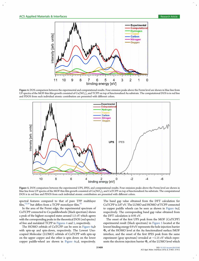
connected to Cu paddlewheels were assembled into the MOFstructures. The measured UPS spectrum of free base TCPP incomparison with the calculated DOS structures of both free baseTCPP and CuTCPP are shown in Figures 4 and 5, respectively.The spectrum is background subtracted, and the calculated
DOS curves were shifted to match the peak positions. This wasnecessary since the calculation was performed on a slab of theMOF structure suspended in vacuum, while the physical filmwas deposited on an Au/SAM substrate, which references itselectronic structure to the substrate surface via interface dipoles.The spectrum shows four emission peaks below the Fermi level.The peaks are at 1.5, 3.75, 6.35, and 8.75 eV in both experi-
ment (black) and computed DOS (red). These emissions can bemainly assigned to C 2p, O 1s, N 2p, Cu 2p, and H 1s orbitals.This is evident from the projected DOS curves in Figures 4 and 5,which show the individual contributions from each of the atomicspecies present in the prepared films. The Cu 2p emission peakhas a major and broader contribution from CuTCPP moleculesthan TCPP molecules. Not surprisingly, this peak is alsothe emission feature that shows the most significant differencesrelative to the spectrum measured on a pure TCPP film.15 It isdenoted from various experiments found in literature that thereare significant similarities between UPS spectral features of meta-lated and H2-porphyrin or H2 phthalocyanine thin films.13,15
This concludes that the experimental electronic structure of thedepositedMOFmultilayer film Figure 4 has similar distinguished
Figure 3. LIXPS and UP spectra before and after step-by-step incubation of sputter cleaned Au functionalized substrate in (A) in the metal ionCu(NO3)2 then in the organic ligands TCPP for three cycles sequentially, (B) in both the metal ion and the organic ligand solution for three cyclessequentially, and (C) only in a TCPP solution for two cycles. Their normalized secondary edges were measured with LIXPS before (LIXPSa) and after(LIXPSb) UPS and are shown in the left panel. The complete normalized UP spectra are displayed in the middle. The right panel shows the evolution ofthe valence band/HOMO emission features through the deposition process.
ACS Applied Materials & Interfaces Research Article
DOI: 10.1021/acsami.6b10340ACS Appl. Mater. Interfaces 2016, 8, 31403−31412
31408
spectral features compared to that of pure TPP multilayerfilm,13,16 but differs from a TCPP monolayer film.43
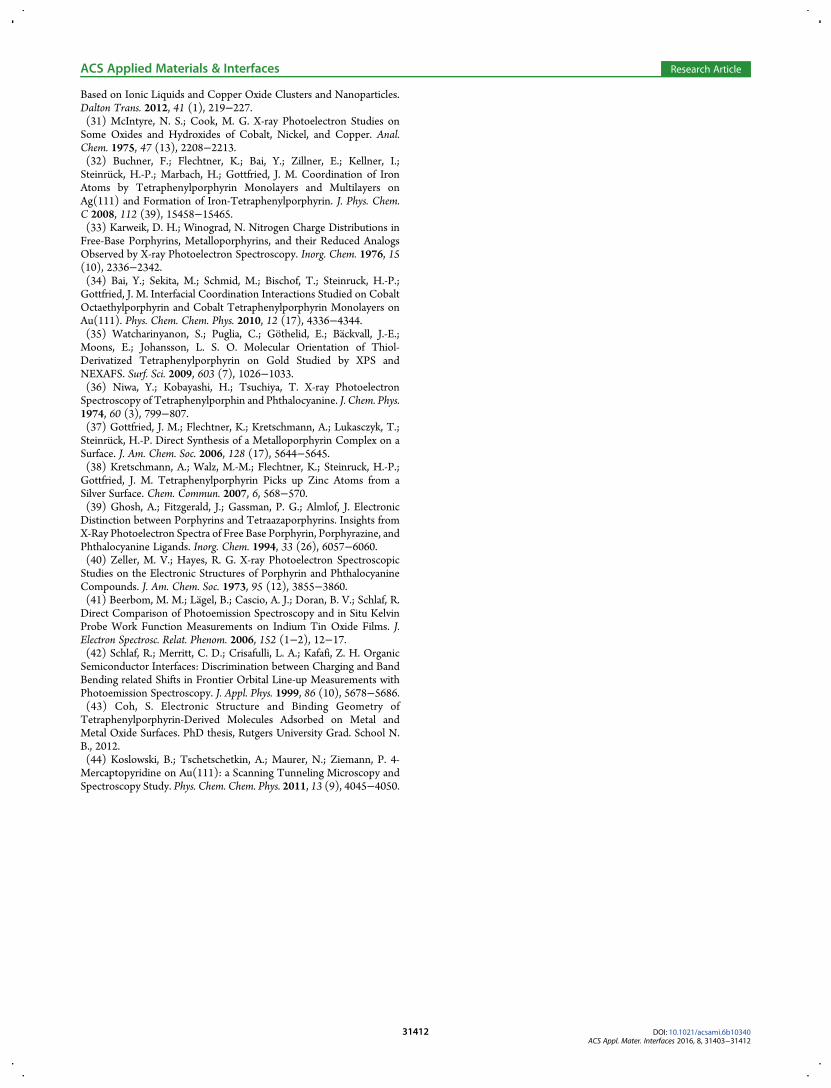
In the area of the Fermi edge, the experimental spectrum ofCuTCPP connected to Cu-paddlewheels (black spectrum) showsa peak of the highest occupied states around 1.5 eV which agreeswith the corresponding peaks in the theoretical DOS (red spectra)of free and metalated TCPP in Figures 4 and 5, respectively.The HOMO orbitals of CuTCPP can be seen in Figure 6a,b
with spin-up and spin-down, respectively. The Lowest Uno-ccupied Molecular (LUMO) orbitals of CuTCPP with spin-upon the upper copper and the other is spin down on the lowercopper paddle-wheel are shown in Figure 6c,d, respectively.
The band gap value obtained from the DFT calculation forCuTCPP is 2.07 eV. The LUMO andHOMOof TCPP connectedto copper paddle wheels can be seen as shown in Figure 6e,f,respectively. The corresponding band gap value obtained fromthe DFT calculation is 0.95 eV.The onset of the first UPS peak from the MOF (CuTCPP)
experimental result (black spectrum) in Figure 5 located at thelowest binding energy 0.9 eV represents the hole injection barrierΦh of the HOMO level at the Au functionalized surface/MOFinterface, and the onset of the first IPES peak from the sameexperiment (gray spectrum) revealed at −1.15 eV which repre-sents the electron injection barrier Φe of the LUMO level which
Figure 5. DOS comparison between the experimental UPS, IPES, and computational results. Four emission peaks above the Fermi level are shown inblue line from UP spectra of the MOF thin film growth consisted of Cu(NO3)2 and CuTCPP on top of functionalized Au substrate. The computationalDOS is in red line and PDOS from each individual atomic contribution are presented with different colors.
Figure 4.DOS comparison between the experimental and computational results. Four emission peaks above the Fermi level are shown in blue line fromUP spectra of theMOF thin film growth consisted of Cu(NO3)2 and TCPP on top of functionalized Au substrate. The computational DOS is in red lineand PDOS from each individual atomic contribution are presented with different colors.
ACS Applied Materials & Interfaces Research Article
DOI: 10.1021/acsami.6b10340ACS Appl. Mater. Interfaces 2016, 8, 31403−31412
31409
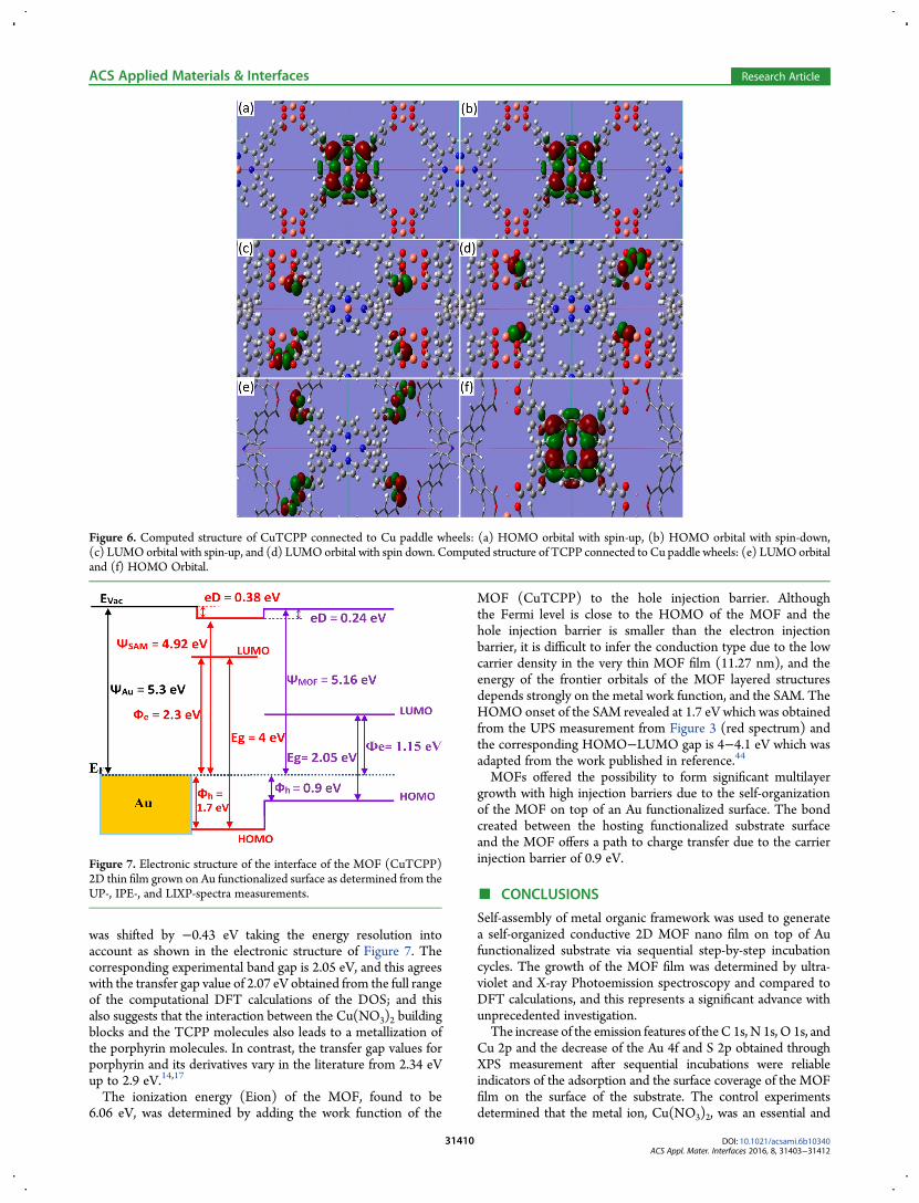
was shifted by −0.43 eV taking the energy resolution intoaccount as shown in the electronic structure of Figure 7. Thecorresponding experimental band gap is 2.05 eV, and this agreeswith the transfer gap value of 2.07 eV obtained from the full rangeof the computational DFT calculations of the DOS; and thisalso suggests that the interaction between the Cu(NO3)2 buildingblocks and the TCPP molecules also leads to a metallization ofthe porphyrin molecules. In contrast, the transfer gap values forporphyrin and its derivatives vary in the literature from 2.34 eVup to 2.9 eV.14,17
The ionization energy (Eion) of the MOF, found to be6.06 eV, was determined by adding the work function of the
MOF (CuTCPP) to the hole injection barrier. Althoughthe Fermi level is close to the HOMO of the MOF and thehole injection barrier is smaller than the electron injectionbarrier, it is difficult to infer the conduction type due to the lowcarrier density in the very thin MOF film (11.27 nm), and theenergy of the frontier orbitals of the MOF layered structuresdepends strongly on the metal work function, and the SAM. TheHOMO onset of the SAM revealed at 1.7 eV which was obtainedfrom the UPS measurement from Figure 3 (red spectrum) andthe corresponding HOMO−LUMO gap is 4−4.1 eV which wasadapted from the work published in reference.44
MOFs offered the possibility to form significant multilayergrowth with high injection barriers due to the self-organizationof the MOF on top of an Au functionalized surface. The bondcreated between the hosting functionalized substrate surfaceand the MOF offers a path to charge transfer due to the carrierinjection barrier of 0.9 eV.
■ CONCLUSIONS
Self-assembly of metal organic framework was used to generatea self-organized conductive 2D MOF nano film on top of Aufunctionalized substrate via sequential step-by-step incubationcycles. The growth of the MOF film was determined by ultra-violet and X-ray Photoemission spectroscopy and compared toDFT calculations, and this represents a significant advance withunprecedented investigation.The increase of the emission features of theC 1s, N 1s, O 1s, and
Cu 2p and the decrease of the Au 4f and S 2p obtained throughXPS measurement after sequential incubations were reliableindicators of the adsorption and the surface coverage of the MOFfilm on the surface of the substrate. The control experimentsdetermined that the metal ion, Cu(NO3)2, was an essential and
Figure 6. Computed structure of CuTCPP connected to Cu paddle wheels: (a) HOMO orbital with spin-up, (b) HOMO orbital with spin-down,(c) LUMOorbital with spin-up, and (d) LUMOorbital with spin down. Computed structure of TCPP connected to Cu paddle wheels: (e) LUMOorbitaland (f) HOMO Orbital.
Figure 7. Electronic structure of the interface of the MOF (CuTCPP)2D thin film grown on Au functionalized surface as determined from theUP-, IPE-, and LIXP-spectra measurements.
ACS Applied Materials & Interfaces Research Article
DOI: 10.1021/acsami.6b10340ACS Appl. Mater. Interfaces 2016, 8, 31403−31412
31410

suitable SBU as a linker between SAM and the arm groups oforganic ligand.The UPS results revealed the orbitals line-up of the MOF
molecules bound to the surface of the Au-functionalized surfaceand revealed similar emission spectral features in correlation withDFT calculations. The combined results from the first onsets ofUP- and IPE-spectra revealed the band gap which strongly agreeswith the value obtained from DFT calculations. The orbitalline-up showed significant barriers for both hole and electroninjections from the Au functionalized surface to the MOF thinfilm, and this property at the interface is crucial to the designand development of conductive MOF materials that can offer animportant breakthrough in molecular electronic devices.
■ AUTHOR INFORMATION
Corresponding Author*E-mail: [email protected] (R.S.).
Author ContributionsThe manuscript was written through contributions of all authors.All authors have given approval to the final version of the manu-script.
NotesThe authors declare no competing financial interest.
■ ACKNOWLEDGMENTS
R.S. gratefully acknowledges the funding from the NationalScience Foundation (grant# NSF DMR-1035196).
■ REFERENCES(1) Li, J.-R.; Kuppler, R. J.; Zhou, H.-C. Selective Gas Adsorption andSeparation in Metal-Organic Frameworks. Chem. Soc. Rev. 2009, 38 (5),1477−1504.(2) Zou, R.-Q.; Sakurai, H.; Xu, Q. Preparation, Adsorption Properties,and Catalytic Activity of 3D Porous Metal−Organic FrameworksComposed of Cubic Building Blocks and Alkali-Metal Ions. Angew.Chem., Int. Ed. 2006, 45 (16), 2542−2546.(3) Luo, J.; Xu, H.; Liu, Y.; Zhao, Y.; Daemen, L. L.; Brown, C.;Timofeeva, T. V.; Ma, S.; Zhou, H.-C. Hydrogen Adsorption in a HighlyStable Porous Rare-Earth Metal-Organic Framework: Sorption Proper-ties and Neutron Diffraction Studies. J. Am. Chem. Soc. 2008, 130 (30),9626−9627.(4) Long, J. R.; Yaghi, O. M. The Pervasive Chemistry of Metal-Organic Frameworks. Chem. Soc. Rev. 2009, 38 (5), 1213−1214.(5) Horcajada, P.; Serre, C.; Vallet-Regí, M.; Sebban, M.; Taulelle, F.;Ferey, G. Metal−Organic Frameworks as Efficient Materials for DrugDelivery. Angew. Chem., Int. Ed. 2006, 45 (36), 5974−5978.(6) Suh, M. P.; Cheon, Y. E.; Lee, E. Y. Syntheses and Functions ofPorous Metallosupramolecular Networks. Coord. Chem. Rev. 2008, 252(8−9), 1007−1026.(7) Yoon, S. M.; Warren, S. C.; Grzybowski, B. A. Storage of ElectricalInformation in Metal−Organic-Framework Memristors. Angew. Chem.,Int. Ed. 2014, 53 (17), 4437−4441.(8) Chua, L. O.; Sung, M. K. Memristive Devices and Systems. Proc.IEEE 1976, 64 (2), 209−223.(9) Strukov, D. B.; Snider, G. S.; Stewart, D. R.; Williams, R. S. TheMissing Memristor Found. Nature 2008, 453 (7191), 80−83.(10) Narayan, T. C.; Miyakai, T.; Seki, S.; Dinca, M. High ChargeMobility in a Tetrathiafulvalene-Based Microporous Metal−OrganicFramework. J. Am. Chem. Soc. 2012, 134 (31), 12932−12935.(11) Wan, S.; Guo, J.; Kim, J.; Ihee, H.; Jiang, D. A Belt-Shaped, BlueLuminescent, and Semiconducting Covalent Organic Framework.Angew. Chem. 2008, 120 (46), 8958−8962.(12) Wan, S.; Guo, J.; Kim, J.; Ihee, H.; Jiang, D. A PhotoconductiveCovalent Organic Framework: Self-Condensed Arene Cubes Com-
posed of Eclipsed 2D Polypyrene Sheets for Photocurrent Generation.Angew. Chem., Int. Ed. 2009, 48 (30), 5439−5442.(13) Lukasczyk, T.; Flechtner, K.; Merte, L. R.; Jux, N.; Maier, F.;Gottfried, J. M.; Steinruck, H.-P. Interaction of Cobalt(II) Tetraar-ylporphyrins with a Ag(111) Surface Studied with PhotoelectronSpectroscopy. J. Phys. Chem. C 2007, 111 (7), 3090−3098.(14) Rojas, G.; Chen, X.; Bravo, C.; Kim, J.-H.; Kim, J.-S.; Xiao, J.;Dowben, P. A.; Gao, Y.; Zeng, X. C.; Choe, W.; Enders, A. Self-Assemblyand Properties of Nonmetalated Tetraphenyl-Porphyrin on MetalSubstrates. J. Phys. Chem. C 2010, 114 (20), 9408−9415.(15) Nardi, M. V.; Detto, F.; Aversa, L.; Verucchi, R.; Salviati, G.;Iannotta, S.; Casarin, M. Electronic Properties of CuPc and H2Pc: anExperimental and Theoretical Study. Phys. Chem. Chem. Phys. 2013, 15(31), 12864−12881.(16) Rojas, G. Self Assembly and Interface Chemistry of Non-Metallated Tetraphenyl Porphyrin. PhD thesis, University of Nebras-kaLincoln: Lincoln, 2011.(17) He, C.; He, Q.; Deng, C.; Shi, L.; Zhu, D.; Fu, Y.; Cao, H.; Cheng,J. Turn on Fluorescence Sensing of Vapor Phase Electron DonatingAmines via Tetraphenylporphyrin or Metallophenylporphrin DopedPolyfluorene. Chem. Commun. 2010, 46 (40), 7536−7538.(18)Wolak, M. u. A.; Balaeff, A.; Gutmann, S.; Helmrich, H. J.; Vosloo,R.; Beerbom, M. M.; Wierzbinski, E.; Waldeck, D. H.; Bezer, S.; Achim,C.; Beratan, D. N.; Schlaf, R. Electronic Structure of Self-AssembledPeptide Nucleic Acid Thin Films. J. Phys. Chem. C 2011, 115 (34),17123−17135.(19) Wolak, M. The Electronic Structure of Biomolecular Self-Assembled Monolayers. PhD thesis, University of South Florida:Tampa, 2012.(20) Xu, G.; Yamada, T.; Otsubo, K.; Sakaida, S.; Kitagawa, H. Facile“Modular Assembly” for Fast Construction of a Highly OrientedCrystalline MOF Nanofilm. J. Am. Chem. Soc. 2012, 134 (40), 16524−16527.(21) Seah, M. P.; Briggs, D. Practical Surf. Anal. Auger X-RayPhotoelectron Spectrosc.; John Wiley & Sons: New York, 1990.(22) Manolova, M.; Ivanova, V.; Kolb, D.; Boyen, H.-G.; Ziemann, P.;Buttner, M.; Romanyuk, A.; Oelhafen, P. Metal Deposition onto Thiol-Covered Gold: Platinum on a 4-Mercaptopyridine SAM. Surf. Sci. 2005,590 (2), 146−153.(23) Boeckl, M. S.; Bramblett, A. L.; Hauch, K. D.; Sasaki, T.; Ratner, B.D.; Rogers, J. W. Self-Assembly of Tetraphenylporphyrin Monolayerson Gold Substrates. Langmuir 2000, 16 (13), 5644−5653.(24) Bramblett, A. L.; Boeckl, M. S.; Hauch, K. D.; Ratner, B. D.; Sasaki,T.; Rogers, J. W. Determination of Surface Coverage for Tetraphe-nylporphyrin Monolayers using Ultraviolet Visible Absorption and X-ray Photoelectron Spectroscopies. Surf. Interface Anal. 2002, 33 (6),506−515.(25) High Resolution XPS of Organic Polymers: The ScientaESCA300 Database Beamson, G.; Briggs, D. J. Chem. Educ. 1993, 70(1), A25.(26) Bai, Y. Photoelectron Spectroscopic Investigations of Porphyrinsand Phthalocyanines on Ag (111) and Au (111): Adsorption andReactivity. PhD thesis, Friedrich-Alexander-Universitat Erlangen−Nurnberg, 2010.(27) Pellegrino, G.; Condorelli, G. G.; Privitera, V.; Cafra, B.; DiMarco, S.; Alberti, A. Dye-Sensitizing of Self-Nanostructured Ti(:Zn)-O2/AZO Transparent Electrodes by Self-Assembly of 5,10,15,20-Tetrakis(4-carboxyphenyl)porphyrin. J. Phys. Chem. C 2011, 115 (15),7760−7767.(28) Li, Z.; Berger, H.; Okamoto, K.; Zhang, Q.; Luscombe, C. K.; Cao,G.; Schlaf, R. Measurement of the Internal Orbital Alignment ofOligothiophene-TiO2 Nanoparticle Hybrids. J. Phys. Chem. C 2013, 117(27), 13961−13970.(29) Wiggins, B. C. Structural and Electronic Properties of Porphyrinsand Phthalocyanines Self Assembled on Conductive Surfaces. Ph.D.,Washington State University, Pullman, WA, 2013.(30) Swadzba-Kwasny, M.; Chancelier, L.; Ng, S.; Manyar, H. G.;Hardacre, C.; Nockemann, P. Facile in Situ Synthesis of Nanofluids
ACS Applied Materials & Interfaces Research Article
DOI: 10.1021/acsami.6b10340ACS Appl. Mater. Interfaces 2016, 8, 31403−31412
31411
Based on Ionic Liquids and Copper Oxide Clusters and Nanoparticles.Dalton Trans. 2012, 41 (1), 219−227.(31) McIntyre, N. S.; Cook, M. G. X-ray Photoelectron Studies onSome Oxides and Hydroxides of Cobalt, Nickel, and Copper. Anal.Chem. 1975, 47 (13), 2208−2213.(32) Buchner, F.; Flechtner, K.; Bai, Y.; Zillner, E.; Kellner, I.;Steinruck, H.-P.; Marbach, H.; Gottfried, J. M. Coordination of IronAtoms by Tetraphenylporphyrin Monolayers and Multilayers onAg(111) and Formation of Iron-Tetraphenylporphyrin. J. Phys. Chem.C 2008, 112 (39), 15458−15465.(33) Karweik, D. H.; Winograd, N. Nitrogen Charge Distributions inFree-Base Porphyrins, Metalloporphyrins, and their Reduced AnalogsObserved by X-ray Photoelectron Spectroscopy. Inorg. Chem. 1976, 15(10), 2336−2342.(34) Bai, Y.; Sekita, M.; Schmid, M.; Bischof, T.; Steinruck, H.-P.;Gottfried, J. M. Interfacial Coordination Interactions Studied on CobaltOctaethylporphyrin and Cobalt Tetraphenylporphyrin Monolayers onAu(111). Phys. Chem. Chem. Phys. 2010, 12 (17), 4336−4344.(35) Watcharinyanon, S.; Puglia, C.; Gothelid, E.; Backvall, J.-E.;Moons, E.; Johansson, L. S. O. Molecular Orientation of Thiol-Derivatized Tetraphenylporphyrin on Gold Studied by XPS andNEXAFS. Surf. Sci. 2009, 603 (7), 1026−1033.(36) Niwa, Y.; Kobayashi, H.; Tsuchiya, T. X-ray PhotoelectronSpectroscopy of Tetraphenylporphin and Phthalocyanine. J. Chem. Phys.1974, 60 (3), 799−807.(37) Gottfried, J. M.; Flechtner, K.; Kretschmann, A.; Lukasczyk, T.;Steinruck, H.-P. Direct Synthesis of a Metalloporphyrin Complex on aSurface. J. Am. Chem. Soc. 2006, 128 (17), 5644−5645.(38) Kretschmann, A.; Walz, M.-M.; Flechtner, K.; Steinruck, H.-P.;Gottfried, J. M. Tetraphenylporphyrin Picks up Zinc Atoms from aSilver Surface. Chem. Commun. 2007, 6, 568−570.(39) Ghosh, A.; Fitzgerald, J.; Gassman, P. G.; Almlof, J. ElectronicDistinction between Porphyrins and Tetraazaporphyrins. Insights fromX-Ray Photoelectron Spectra of Free Base Porphyrin, Porphyrazine, andPhthalocyanine Ligands. Inorg. Chem. 1994, 33 (26), 6057−6060.(40) Zeller, M. V.; Hayes, R. G. X-ray Photoelectron SpectroscopicStudies on the Electronic Structures of Porphyrin and PhthalocyanineCompounds. J. Am. Chem. Soc. 1973, 95 (12), 3855−3860.(41) Beerbom, M. M.; Lagel, B.; Cascio, A. J.; Doran, B. V.; Schlaf, R.Direct Comparison of Photoemission Spectroscopy and in Situ KelvinProbe Work Function Measurements on Indium Tin Oxide Films. J.Electron Spectrosc. Relat. Phenom. 2006, 152 (1−2), 12−17.(42) Schlaf, R.; Merritt, C. D.; Crisafulli, L. A.; Kafafi, Z. H. OrganicSemiconductor Interfaces: Discrimination between Charging and BandBending related Shifts in Frontier Orbital Line-up Measurements withPhotoemission Spectroscopy. J. Appl. Phys. 1999, 86 (10), 5678−5686.(43) Coh, S. Electronic Structure and Binding Geometry ofTetraphenylporphyrin-Derived Molecules Adsorbed on Metal andMetal Oxide Surfaces. PhD thesis, Rutgers University Grad. School N.B., 2012.(44) Koslowski, B.; Tschetschetkin, A.; Maurer, N.; Ziemann, P. 4-Mercaptopyridine on Au(111): a Scanning Tunneling Microscopy andSpectroscopy Study. Phys. Chem. Chem. Phys. 2011, 13 (9), 4045−4050.
ACS Applied Materials & Interfaces Research Article
DOI: 10.1021/acsami.6b10340ACS Appl. Mater. Interfaces 2016, 8, 31403−31412
31412