Photoemission Electron Spectroscopy IV: Angle … No.2/Vol.17 No.2...Photoemission electron...
23
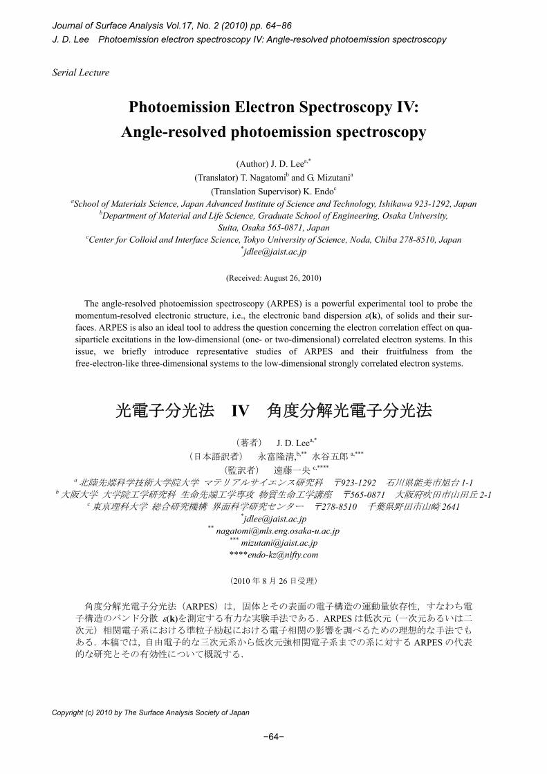
Journal of Surface Analysis Vol.17, No. 2 (2010) pp. 64−86 J. D. Lee Photoemission electron spectroscopy IV: Angle-resolved photoemission spectroscopy −64− Serial Lecture Photoemission Electron Spectroscopy IV: Angle-resolved photoemission spectroscopy (Author) J. D. Lee a,* (Translator) T. Nagatomi b and G. Mizutani a (Translation Supervisor) K. Endo c a School of Materials Science, Japan Advanced Institute of Science and Technology, Ishikawa 923-1292, Japan b Department of Material and Life Science, Graduate School of Engineering, Osaka University, Suita, Osaka 565-0871, Japan c Center for Colloid and Interface Science, Tokyo University of Science, Noda, Chiba 278-8510, Japan * [email protected] (Received: August 26, 2010) The angle-resolved photoemission spectroscopy (ARPES) is a powerful experimental tool to probe the momentum-resolved electronic structure, i.e., the electronic band dispersion ε(k), of solids and their sur- faces. ARPES is also an ideal tool to address the question concerning the electron correlation effect on qua- siparticle excitations in the low-dimensional (one- or two-dimensional) correlated electron systems. In this issue, we briefly introduce representative studies of ARPES and their fruitfulness from the free-electron-like three-dimensional systems to the low-dimensional strongly correlated electron systems. 光電子分光法 IV 角度分解光電子分光法 (著者) J. D. Lee a,* (日本語訳者) 永富隆清, b,** 水谷五郎 a,*** (監訳者) 遠藤一央 c,**** a 北陸先端科学技術大学院大学 マテリアルサイエンス研究科 〒923-1292 石川県能美市旭台 1-1 b 大阪大学 大学院工学研究科 生命先端工学専攻 物質生命工学講座 〒565-0871 大阪府吹田市山田丘 2-1 c 東京理科大学 総合研究機構 界面科学研究センター 〒278-8510 千葉県野田市山崎 2641 * [email protected] ** [email protected] *** [email protected] ****[email protected] (2010 年 8 月 26 日受理) 角度分解光電子分光法(ARPES)は,固体とその表面の電子構造の運動量依存性,すなわち電 子構造のバンド分散 ε(k)を測定する有力な実験手法である. ARPES は低次元(一次元あるいは二 次元)相関電子系における準粒子励起における電子相関の影響を調べるための理想的な手法でも ある.本稿では,自由電子的な三次元系から低次元強相関電子系までの系に対する ARPES の代表 的な研究とその有効性について概説する. Copyright (c) 2010 by The Surface Analysis Society of Japan
Transcript of Photoemission Electron Spectroscopy IV: Angle … No.2/Vol.17 No.2...Photoemission electron...
Journal of Surface Analysis Vol.17, No. 2 (2010) pp. 64−86 J. D. Lee Photoemission electron spectroscopy IV: Angle-resolved photoemission spectroscopy
−64−
Serial Lecture
Photoemission Electron Spectroscopy IV: Angle-resolved photoemission spectroscopy
(Author) J. D. Leea,*
(Translator) T. Nagatomib and G. Mizutania (Translation Supervisor) K. Endoc
aSchool of Materials Science, Japan Advanced Institute of Science and Technology, Ishikawa 923-1292, Japan bDepartment of Material and Life Science, Graduate School of Engineering, Osaka University,
Suita, Osaka 565-0871, Japan cCenter for Colloid and Interface Science, Tokyo University of Science, Noda, Chiba 278-8510, Japan
(Received: August 26, 2010)
The angle-resolved photoemission spectroscopy (ARPES) is a powerful experimental tool to probe the momentum-resolved electronic structure, i.e., the electronic band dispersion ε(k), of solids and their sur-faces. ARPES is also an ideal tool to address the question concerning the electron correlation effect on qua-siparticle excitations in the low-dimensional (one- or two-dimensional) correlated electron systems. In this issue, we briefly introduce representative studies of ARPES and their fruitfulness from the free-electron-like three-dimensional systems to the low-dimensional strongly correlated electron systems.
光電子分光法 IV 角度分解光電子分光法
(著者) J. D. Leea,* (日本語訳者) 永富隆清,b,** 水谷五郎 a,***
(監訳者) 遠藤一央 c,**** a北陸先端科学技術大学院大学 マテリアルサイエンス研究科 〒923-1292 石川県能美市旭台 1-1
b大阪大学 大学院工学研究科 生命先端工学専攻 物質生命工学講座 〒565-0871 大阪府吹田市山田丘 2-1 c東京理科大学 総合研究機構 界面科学研究センター 〒278-8510 千葉県野田市山崎 2641
*[email protected] ** [email protected]
*** [email protected] ****[email protected]
(2010 年 8 月 26 日受理)
角度分解光電子分光法(ARPES)は,固体とその表面の電子構造の運動量依存性,すなわち電
子構造のバンド分散 ε(k)を測定する有力な実験手法である.ARPES は低次元(一次元あるいは二
次元)相関電子系における準粒子励起における電子相関の影響を調べるための理想的な手法でも
ある.本稿では,自由電子的な三次元系から低次元強相関電子系までの系に対する ARPES の代表
的な研究とその有効性について概説する.
Copyright (c) 2010 by The Surface Analysis Society of Japan
Journal of Surface Analysis Vol.17, No. 2 (2010) pp. 64−86 J. D. Lee Photoemission electron spectroscopy IV: Angle-resolved photoemission spectroscopy
−65−
1. Introduction Photoemission electron spectroscopy (PES) makes it
possible to directly probe the electronic structure of an atom, a molecule, or a solid by measuring the binding energies of electrons emitted from the electronic states of the corresponding matter [1-3]. Angle-resolved photo-emission spectroscopy (ARPES) is one of variants of PES and a highly advanced spectroscopic method, where both momentum and kinetic energy of the electrons pho-toemitted from a sample are measured so that the mo-mentum-resolved (i.e., not only magnitude- but also di-rection-resolved) probe is available [4-6]. ARPES is one of the most direct and powerful methods of studying the electronic structure dispersive with the crystal momen-tum in strongly anisotropic systems and especially essen-tial for the investigation of the electron correlation ef-fects of low-dimensional (one- or two-dimensional) cor-related electron systems [7].
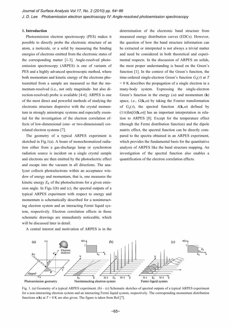
The geometry of a typical ARPES experiment is sketched in Fig.1(a). A beam of monochromatized radia-tion either from a gas-discharge lamp or synchrotron radiation source is incident on a single crystal sample and electrons are then emitted by the photoelectric effect and escape into the vacuum in all directions. The ana-lyzer collects photoelectrons within an acceptance win-dow of energy and momentum, that is, one measures the kinetic energy EK of the photoelectrons for a given emis-sion angle. In Figs.1(b) and (c), the spectral outputs of a typical ARPES experiment with respect to energy and momentum is schematically described for a noninteract-ing electron system and an interacting Fermi liquid sys-tem, respectively. Electron correlation effects in those schematic drawings are immediately noticeable, which will be discussed later in detail.
A central interest and motivation of ARPES is in the
determination of the electronic band structure from measured energy distribution curves (EDCs). However, the question of how the band structure information can be extracted or interpreted is not always a trivial matter and need be considered in both theoretical and experi-mental respects. In the discussion of ARPES on solids, the most proper understanding is based on the Green’s function [1]. In the context of the Green’s function, the time-ordered single-electron Green’s function Gij(τ) at T = 0 K describes the propagation of a single electron in a many-body system. Expressing the single-electron Green’s function in the energy (ω) and momentum (k) space, i.e., G(k,ω) by taking the Fourier transformation of Gij(τ), the spectral function A(k,ω) defined by (1/π)Im[G(k,ω)] has an important interpretation in rela-tion to ARPES [8]. Except for the temperature effect (through the Fermi distribution function) and the dipole matrix effect, the spectral function can be directly com-pared to the spectra obtained in an ARPES experiment, which provides the fundamental basis for the quantitative analysis of ARPES like the band structure mapping. An investigation of the spectral function also enables a quantification of the electron correlation effects.
Fig. 1. (a) Geometry of a typical ARPES experiment. (b) – (c) Schematic sketches of spectral outputs of a typical ARPES experiment for a non-interacting electron system and an interacting Fermi liquid system, respectively. The corresponding momentum distribution functions n(k) at T = 0 K are also given. The figure is taken from Ref.[7].
Journal of Surface Analysis Vol.17, No. 2 (2010) pp. 64−86 J. D. Lee Photoemission electron spectroscopy IV: Angle-resolved photoemission spectroscopy
−66−
1. はじめに 光電子分光法(PES)では,物質中のある電子状
態から放出される電子の結合エネルギーを測定する
ことで,原子や分子,あるいは固体の電子構造を直
接調べることができる[1-3].角度分解光電子分光法
(ARPES)は PES の一種で,試料から放出される光
電子の運動量と運動エネルギーを共に測定すること
で,電子状態の運動量依存性(すなわち,強度だけ
でなく放出角度分布も)を調べることができる非常
に優れた分光法である[4-6].ARPES は,非常に異方
的なバンド構造を持つ系における電子構造の結晶運
動量依存性を直接調べることができる強力な手法で
あり,特に低次元(一次元あるいは二次元)相関電
子系における電子相関の効果を調べるために不可欠
な手法である[7]. ARPES の典型的な測定系を図 1(a)に示す.単色化
された放電ランプからの光や放射光を単結晶試料へ
照射すると,光電効果によって真空中のあらゆる方
向へ電子が放出される.この放出された光電子のう
ち,あるエネルギーと運動量を持つもののみを検出
する.すなわち,ある放出角度で放出された光電子
の運動エネルギーEKを測定する.図 1(b)及び(c)にそ
れぞれ相互作用のない電子系及び相互作用のある
フェルミ液体系に対して得られる ARPES スペクト
ルの例を模式的に示す.図 1(b)及び(c)から,電子相
関の効果がある場合にどのようなスペクトルが得ら
れるか容易に理解できるが,この点については詳細
に後述する. ARPES における中心的な興味と研究に対する動
機は,測定によって得られるエネルギー分布曲線
(ESCs: energy distribution curves)から電子バンド構
造を決定することである.しかしながら,どのよう
にバンド構造情報を抽出して説明するかは必ずしも
簡単でなく,理論と実験の両面から考察することが
必要である.固体に対する ARPES の議論では,
も適切な理解はグリーン関数に基づいたものである
[1].グリーン関数法では,T = 0 K での時間発展一電
子グリーン関数 Gij(τ)は多電子系における一電子の
運動を記述する.Gij(τ)をフーリエ変換したエネル
ギー(ω)及び運動量(k)空間での一電子グリーン
関数を G(k,ω)で表すと,(1/π)Im[G(k,ω)]で与えられ
るスペクトル関数 A(k,ω)は ARPES に関する重要な
解釈を与える[8].フェルミ分布関数で記述される温
度の効果と双極子マトリクス効果を除いて,スペク
トル関数は ARPES 測定によって得られるスペクト
ルと直接比較することができ,バンド構造マッピン
グのような ARPES の定量的な解析に対する基礎的
な知見を与える.またスペクトル関数を調べること
で,電子相関効果を定量的に取り扱うこともできる.
Journal of Surface Analysis Vol.17, No. 2 (2010) pp. 64−86 J. D. Lee Photoemission electron spectroscopy IV: Angle-resolved photoemission spectroscopy
−67−
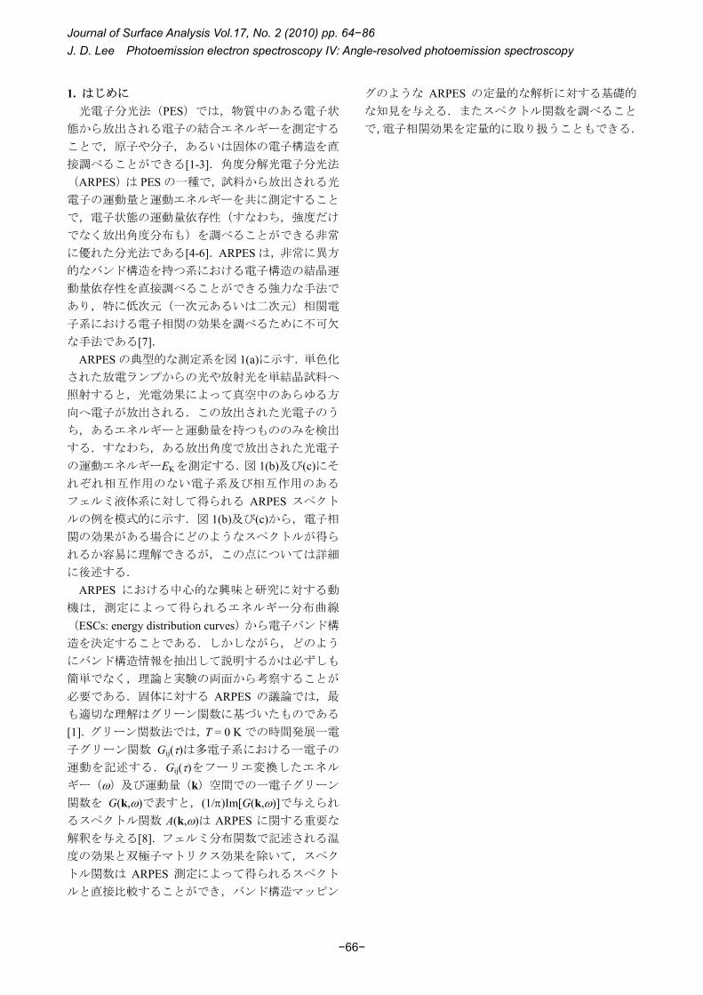
On the other hand, due to a conversion problem be-tween the photoelectron momentum and the crystal mo-mentum of the corresponding band structure, nontrivial difficulties occur in a direct comparison with an ARPES experiment. Of course, the photoelectron momentum K is perfectly resolved: under the geometry of Fig.1(a),
θsin2 K|| mE=K , or further ϕθ cossin2 KmEx =K and ϕθ sinsin2 KmEy =K , and θcos2 KmE=⊥K . The goal is to determine the electronic dispersion ε(k) with the crystal momentum k for the solid left behind from the photoelectron with K. For the momentum par-allel to the surface, K|| determines k|| exactly within the reciprocal lattice vector G, that is, K||=k||+G. However, for the momentum perpendicular to the surface, the situation is rather complex because there is no direct re-lation between ⊥K (and/or K||) and ⊥k .To overcome this problem, one in fact needs a priori assumption or knowledge about the final state, for example, from the simple so-called “free-electron model” (as shown in Fig.2) or from the band structure calculation. But there is also a case where one can avoid this problem. In the low-dimensional (one- or two-dimensional) electron systems, one does not have to determine ⊥k so that the difficulty due to the problem does not occur in principle. This is the reason why ARPES is an ideal tool to study the electronic structure of the low-dimensional electron systems.
The free-electron model for the final states is basically expected to work well for materials with the Fermi sphere of a simple spherical topology, most likely for alkali metals. But as a matter of fact, it is often applied also for much more complicated three-dimensional sys-tems even if the initial state is far from the
free-electron-like state. On the other hand, as mentioned previously, ARPES is ideal for the low-dimensional sys-tems. The success of ARPES study in the last few dec-ades for the high Tc superconductors, probably one of the hottest materials in the modern materials science, is remarkable [9]. The high Tc superconductor is a well-known two-dimensional system, where the elec-tronic conduction occurs mostly in the CuO2 plane. Re-cently, ARPES is also making essential roles in the sys-tems of graphite or layered graphene which attracts great attention as a seed material for the carbon-based nano-scopic functional materials or a test bed of new charac-teristic fundamental physics [10]. Graphite is a quasi-two-dimensional material of hexagonal atomic carbon layer and graphene is a perfect two-dimensional version of graphite. The electron correlation effects be-come more prominent in a lower-dimensional system. Deeper understanding about the electron correlation could be sought for in the one-dimensional correlated system, for which ARPES also provides good solutions.
Fig. 2. Schematic description of kinematics of photoemission process. (a) Optical transition within reciprocal lattice vector. (b) Free-electron model for final states. (c) Final photoelectron spectra. The figure is taken from Ref.[7].
Journal of Surface Analysis Vol.17, No. 2 (2010) pp. 64−86 J. D. Lee Photoemission electron spectroscopy IV: Angle-resolved photoemission spectroscopy
−68−
一方,対象とするバンド構造における結晶運動量
へ光電子の運動量を変換する際の問題のために,
ARPES の実験結果との直接比較において大きな困
難が伴うことになる.もちろん,光電子の運動量 Kは完全に分解されており,図 1(a)に示した測定条件
で は θsin2 K|| mE=K , あ る い は さ ら に
ϕθ cossin2 KmEx =K 及び ϕθ sinsin2 KmEy =K ,
θcos2 KmE=⊥K である.目標は,運動量 K の光電
子が 1 個抜けた結晶において,結晶運動量 k の関数
として電子構造の分散ε(k)を決定することである.
表面に平行な運動量については,K||から厳密に逆格
子ベクトル G 内の k||,すなわち K||=k||+G が決まる.
しかしながら,表面に垂直な運動量については, ⊥K(及び/あるいは K||)と ⊥k の間に直接的な関係がな
いために状況がより複雑である.この問題を解決す
るために,実際の解析では,例えば,単純な(図 2に示すような)“自由電子モデル”あるいはバンド
構造計算に基づいた終状態に対する事前の仮定や知
識が必要である.しかし,他にもこの問題を避けら
れる場合がある.それは低次元(一次元あるいは二
次元)電子系の場合で, ⊥k を決定する必要がなく,
低次元系では原理的にこの問題は起きない.これが,
低次元電子系の電子構造の研究において ARPES が
理想的な手法である理由である. アルカリ金属のような単純な球状のフェルミ球を
持つ材料においては,自由電子モデルを用いるとそ
の終状態がよく記述できると基本的に予想される.
しかしながら現実問題として,始状態が自由電子的
な状態と異なるような複雑な三次元系においても自
由電子モデルが頻繁に用いられる.一方上述したと
おり,ARPES は低次元系に対しては理想的な手法で
ある.おそらく近代物質科学において も注目され
る材料の一つである高温超電導体のここ数十年間の
研究において ARPES は著しく有効であった[9].高
温超伝導体は,電気伝導が CuO2 面内で起きる二次
元系であることがよく知られている.近年では,炭
素系ナノ機能材料の基礎材料あるいは新しい特徴的
な基礎物理現象の研究のための試験台として大変注
目されているグラファイトや層状グラフェンの研究
において,AREPS は重要な役割を果たしている[10].グラファイトは六方晶炭素原子層を持つ擬二次元材
料であり,グラフェンはグラファイトの完全な二次
元バージョンである.低次元系では電子相関効果が
より顕著になるため,電子相関についてより深く理
解することは一次元電子相関系において重要であり,
ARPES によって適切な理解が得られると考えられ
る.
Journal of Surface Analysis Vol.17, No. 2 (2010) pp. 64−86 J. D. Lee Photoemission electron spectroscopy IV: Angle-resolved photoemission spectroscopy
−69−
2. Fundamentals of ARPES 2.1. Spectral function
The time-ordered single-electron Green’s function Gk(ω) represented in the energy (ω) and momentum space (k) is given by a sum of Gk
<(ω) and Gk>(ω) [1],
which can be formally written down as
( )
( ) ( )ωωεω
εωω
><
+
+
+=+−
+++
−+
−−=
∑
∑
kk
tt
kk
ss
kk
k
GGi
NctNtNcN
i
sNcNNcsNG
0
,1,1
0
,1,1
†
†
(1)
The spectral function A(k,ω) is defined by (1/π)Im[G(k,ω)] and given by A<(k,ω)+A>(k,ω). It is noted that A<(k,ω) and A>(k,ω) treat occupied and unoc-cupied states, respectively, so that they should be com-pared to emission and inverse-emission spectra, i.e., PES and inverse PES (IPES), respectively. The measured ARPES intensity I(k,ω) would then be [11]
( ) ( ) ( )ωωω ,, 2 kk <Δ= AfI k (2)
where |Δk|2 is from the dipole matrix and f(ω) from the Fermi distribution accounting for the temperature effect.
More physical insights could be obtained by introduc-ing the electron self-energy Σ(k,ω) to the Green’s func-tion Gk(ω). In the case, the Green’s function (corre-sponding to the emission part) and its spectral function are
( ) ( )∑−+=
ωεωω
,1,
kk
k
G (3)
( ) ( )( )[ ] ( )∑∑∑
+−+=
22 ,Im,Re
,Im1,ωωεω
ωπ
ωkk
kk
k
A (4)
Further, one can separate the spectral function (or the Green’s function) into a coherent part and an incoherent part
( )( ) inchoh22, AZA
kk
kk +
Γ+−
Γ=
εωπ
ωk (5)
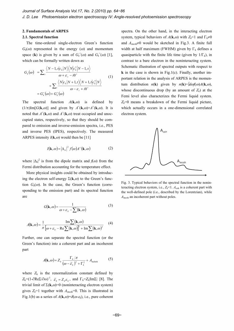
where Zk is the renormalization constant defined by Zk=(1-∂ReΣ/∂ω)-1, kkk Z εε = , and Γk=Zk|ImΣ| [8]. The trivial limit of Σ(k,ω)=0 (noninteracting electron system) gives Zk=1 together with Aincoh=0. This is illustrated in Fig.1(b) as a series of A(k,ω)=δ(ω-εk), i.e., pure coherent
spectra. On the other hand, in the interacting electron system, typical behaviors of A(k,ω) with Zk<1 and Γk≠0 and Aincoh≠0 would be sketched in Fig.3. A finite full width at half maximum (FWHM) given by Γk defines a quasiparticle with the finite life time (given by 1/Γk), in contrast to a bare electron in the noninteracting system. Schematic illustration of spectral outputs with respect to k in the case is shown in Fig.1(c). Finally, another im-portant relation in the analysis of ARPES is the momen-tum distribution n(k) given by n(k)=∫dωf(ω)A(k,ω), whose discontinuous drop (by an amount of Zk) at the Femi level also characterizes the Fermi liquid system. Zk=0 means a breakdown of the Fermi liquid picture, which actually occurs in a one-dimensional correlated electron system.
Fig. 3. Typical behaviors of the spectral function in the nonin-teracting electron system, i.e., Zk<1. Acoh is a coherent part with the well-defined pole (i.e., described by the Lorentzian), while Aincoh an incoherent part without poles.
Journal of Surface Analysis Vol.17, No. 2 (2010) pp. 64−86 J. D. Lee Photoemission electron spectroscopy IV: Angle-resolved photoemission spectroscopy
−70−
2. ARPES の基礎 2.1. スペクトル関数
エネルギー(ω)及び運動量(k)空間で表される
時間発展一電子グリーン関数 Gk(ω)は,Gk<(ω)と
Gk>(ω)の和として与えられ[1],形式的に次式で表さ
れる.
( )
( ) ( )ωωεω
εωω
><
+
+
+=+−
+++
−+
−−=
∑
∑
kk
tt
kk
ss
kk
k
GGi
NctNtNcN
i
sNcNNcsNG
0
,1,1
0
,1,1
†
†
(1)
スペクトル関数 A(k,ω)は(1/π)Im[G(k,ω)]で定義され,
A<(k,ω)+A>(k,ω)で与えられる.ここで A<(k,ω)及び
A>(k,ω)はそれぞれ占有及び非占有状態を扱ってお
り,光電子スペクトル及び逆光電子スペクトル,す
なわち PES 及び逆 PES(IPES)と比較されるべきも
のである.測定される ARPES 強度 I(k,ω)は次式で与
えられる[11].
( ) ( ) ( )ωωω ,, 2 kk <Δ= AfI k (2)
ここで|Δk|2は双極子マトリクス,f(ω)は温度の効果を
記述するフェルミ分布を表している. より物理的な理解は,グリーン関数 Gk(ω)へ電子
の自己エネルギーΣ(k,ω)を導入することで得られる.
この場合,グリーン関数(光電子放出に相当する項)
とそのスペクトル関数は
( ) ( )∑−+=
ωεωω
,1,
kk
k
G (3)
( ) ( )( )[ ] ( )∑∑∑
+−+=
22 ,Im,Re
,Im1,ωωεω
ωπ
ωkk
kk
k
A (4)
で与えられる.さらにスペクトル関数(あるいはグ
リーン関数)はコヒーレントな項とインコヒーレン
トな項に分けることができる.
( )( ) inchoh22, AZA
kk
kk +
Γ+−
Γ=
εωπ
ωk (5)
ここで Zkは Zk=(1-∂ReΣ/∂ω)-1で定義される繰り込み
定数, kε は kkk Z εε = ,Γk はΓk=Zk|ImΣ|である[8].Σ(k,ω)=0 の極限(相互作用しない電子系)では Zk=1及 び Aincoh=0 と 得 ら れ る . こ れ は 一 連 の
A(k,ω)=δ(ω-εk),すなわち純粋なコヒーレントなスペ
クトルとして図 1(b)に示してある.一方,相互作用
する電子系では,Zk<1,Γk≠0 及び Aincoh≠0 として,
A(k,ω)の典型的な振る舞いを図 3 に示す.相互作用
の無い系における裸の電子に対して,Γkで与えられ
る有限の半値全幅(FWHM)は(1/Γkで与えられる)
有限の寿命を持つ準粒子を定義する.この場合の kによって変化するスペクトルは図 1(c)に模式的に示
してある. 後に,AREPS におけるもう一つの重要
な関係は運動量の分布 n(k)が n(k)=∫dωf(ω)A(k,ω)で与えられることであり,そのフェルミ準位での不連
続な(Zk に相当する)減少もまたフェルミ液体系の
特徴である.Zk=0 はフェルミ液体による描像が破綻
することを意味し,これは実際に一次元電子相関系
において起こる現象である.
Journal of Surface Analysis Vol.17, No. 2 (2010) pp. 64−86 J. D. Lee Photoemission electron spectroscopy IV: Angle-resolved photoemission spectroscopy
−71−
2.2. Final states The simplest, most frequently employed model for the
final states is based on the assumption of a free-electron final state. In the model, the dispersion relation of the final state is assumed to be
( ) ( )0*
2
f 2V
mE +
+≈
Gkk (6)
where m* is the effective mass, G the reciprocal lattice vector, and V0 the inner potential (see Fig.2). Under the model, we have a relation of Ef(k)-Ei(k)=hν with the photon energy hν for the optical transition and another relation of EK=Ef(k)-V0 with the photoelectron kinetic energy EK. From an additional relation of k||= K||+G be-tween momenta parallel to the surface, one can deter-mine ⊥k [12]. For the normal emission case (K||=0, i.e., k||=0), the conversion process in order to obtain ( )⊥kiE , i.e., the electronic band dispersion along the direction perpendicular to the surface, would be especially simple.
It is a crystal potential that makes the final state devi-ate from a free-electron one. The effect of the crystal potential gets weaker with increasing kinetic energy of the electron. Therefore, this may imply that the higher the excitation energy, the better the free-electron model.
Reasonable successes of the electronic structure cal-culation at least for metals naturally encourage an im-provement of the free-electron approximation based on the theoretical calculation. In this case, one used to ob-tain the theoretical results using an interpolation scheme to fit the band structure to the data points and compare with the experiment [13]. In addition, there are also a few methods to allow an unbiased comparison with theoretical band structures without involving any a priori assumption. Such methods are not only complicated, but also expensive in that many experimental data are re-quired. One of them is the so-called triangulation (or energy-coincidence) method proposed by Kane [14], which observes a direct transition occurring at a well-defined point of the Brillouin zone (BZ).
2.3. Matrix element effects
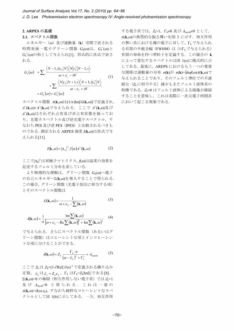
The matrix element |Δk|2 (2
if ˆ kk r φεφ ⋅∝ ) of Eq.(2) is responsible for the dependence of ARPES not only on the emission angle of the photoelectron, but also the photon energy and polarization ( ε̂ ) and other experi-mental geometry [15]. φf
k is the photoelectron state and
φik the initial Bloch state, respectively. It may even result
in a complete suppression of photoemission signal de-pending on the underlying symmetry. Let us consider the mirror plane emission from a
22 yxd
− orbital displayed in
Fig.4 where the detector (i.e., the electron analyzer) is located on the mirror. Without any sophisticated analysis, one may make a few nontrivial arguments concerning the photoemission signal intensity. First, in order to obtain the nonzero signal through the detector on the mirror plane, the photoelectron state φf
k itself must be even. Second, the even photoelectron state subsequently im-plies that kr i|ˆ φε ⋅ must be even to make the overlap integral nonvanishing. Eventually, therefore, in order to obtain the nonzero signal, if φi
k is even (as depicted in Fig.4), one needs to have
pˆˆ εε = (in-plane), otherwise if φi
k is odd, one needs to have sˆˆ εε = (out-of-plane).
Fig. 4. Photoemission from a
22 yxd
− orbital on the mirror
plane (the detector is also located on the mirror plane).
Journal of Surface Analysis Vol.17, No. 2 (2010) pp. 64−86 J. D. Lee Photoemission electron spectroscopy IV: Angle-resolved photoemission spectroscopy
−72−
2.2. 終状態 終状態を記述するために も単純で頻繁に用いら
れるモデルでは,終状態を自由電子で記述できると
仮定する.このモデルでは,終状態の分散関係は次
式で与えられると仮定する.
( ) ( )0*
2
f 2V
mE +
+≈
Gkk (6)
ここで m*は有効質量,G は逆格子ベクトル,V0は内
部ポテンシャルである(図 2 参照).本モデルでは,
光子のエネルギーを hνとすると光学遷移に対して
Ef(k)-Ei(k)=hνの関係が成立し,光電子の運動エネル
ギーEK に対して EK=Ef(k)-V0 の関係も成立する.さ
らに表面に平行な運動量に対する k||= K||+G の関係
から ⊥k を決定することができる[12].試料表面垂直
方向へ電子が放出される場合(K||=0,すなわち k||=0)は, ( )⊥kiE を得るための変換過程,すなわち表面垂
直方向のバンド分散が特に簡単になる. 終状態が自由電子的な振る舞いからずれるのは結
晶ポテンシャルのためである.結晶ポテンシャルの
影響は電子のエネルギーの増加にともなって弱くな
る.それゆえに,励起エネルギーを高くするほど自
由電子モデルでよく記述できると考えられる. 少なくとも金属に対する電子構造計算の理にか
なった成功が,理論計算に基づいた自由電子近似の
改善を後押しするのは自然である.この場合,バン
ド構造をデータ点にフィットして実験結果と比較し
ながら内挿する方法を用いて理論の結果を得るのが
常であった[13].加えて,事前の仮定なしに理論的
に得られたバンド構造を先入観なく比較できるいく
つかのモデルもある.そのような手法は複雑なだけ
でなく多くの実験データが必要であるという欠点も
持つ.そのような手法の一つがいわゆる Kane によっ
て 提 案 さ れ た triangulation ( あ る い は
energy-coincidence)法[14]であり,この手法によって
ブリルアンゾーン(BZ)のよく定義された点で起こ
る直接遷移を調べることができる.
2.3. 行列要素の効果 式(2)の遷移行列|Δk|2(
2
if ˆ kk r φεφ ⋅∝ )は,ARPESの光電子放出角度依存性だけでなく,光子のエネル
ギーと偏光,その他の実験的配置への依存性を記述
するのに重要である[15].φfk は光電子の状態,φi
k は
初期ブロッホ状態である.対称性に依存して光電子
信号を完全に消してしまうこともある.今,図 4 に
示した22 yx
d−
軌道からの鏡面内放出を考える.ここで
検出器(電子分析器)は鏡面上にある.特に複雑な
解析なしで光電子信号強度に関するいくつかの重要
な議論を展開することができる.一つ目は,鏡面上
にある検出器でゼロでない信号強度を得るためには,
光電子状態φfk そのものは偶関数でなければならな
いことである.二つ目は,重なり積分がゼロとなら
ないために,光電子状態が偶関数であることからkr i|ˆ φε ⋅ も偶関数でなければならない点である.そ
れゆえに,結局,ゼロでない信号強度を得るために
は,(図 4 に示すように)φikが偶関数の場合は入射
光偏光についてpˆˆ εε = が成り立つ(in-plane)必要が
あ り , φik が 奇 関 数 の 場 合 は sˆˆ εε = が 成 立
(out-of-plane)しなければならない.
Journal of Surface Analysis Vol.17, No. 2 (2010) pp. 64−86 J. D. Lee Photoemission electron spectroscopy IV: Angle-resolved photoemission spectroscopy
−73−
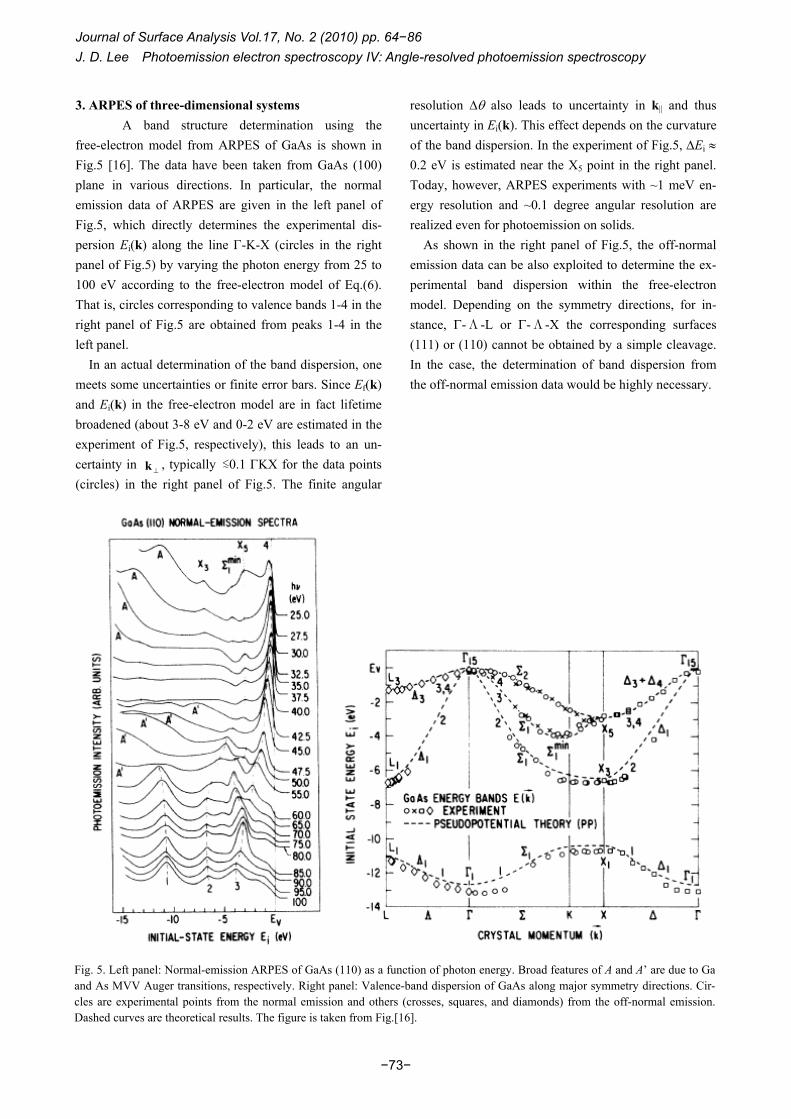
3. ARPES of three-dimensional systems A band structure determination using the
free-electron model from ARPES of GaAs is shown in Fig.5 [16]. The data have been taken from GaAs (100) plane in various directions. In particular, the normal emission data of ARPES are given in the left panel of Fig.5, which directly determines the experimental dis-persion Ei(k) along the line Γ-K-X (circles in the right panel of Fig.5) by varying the photon energy from 25 to 100 eV according to the free-electron model of Eq.(6). That is, circles corresponding to valence bands 1-4 in the right panel of Fig.5 are obtained from peaks 1-4 in the left panel.
In an actual determination of the band dispersion, one meets some uncertainties or finite error bars. Since Ef(k) and Ei(k) in the free-electron model are in fact lifetime broadened (about 3-8 eV and 0-2 eV are estimated in the experiment of Fig.5, respectively), this leads to an un-certainty in ⊥k , typically ≲0.1 ΓKX for the data points (circles) in the right panel of Fig.5. The finite angular
resolution Δθ also leads to uncertainty in k|| and thus uncertainty in Ei(k). This effect depends on the curvature of the band dispersion. In the experiment of Fig.5, ΔEi ≈ 0.2 eV is estimated near the X5 point in the right panel. Today, however, ARPES experiments with ~1 meV en-ergy resolution and ~0.1 degree angular resolution are realized even for photoemission on solids.
As shown in the right panel of Fig.5, the off-normal emission data can be also exploited to determine the ex-perimental band dispersion within the free-electron model. Depending on the symmetry directions, for in-stance, Γ-Λ-L or Γ-Λ-X the corresponding surfaces (111) or (110) cannot be obtained by a simple cleavage. In the case, the determination of band dispersion from the off-normal emission data would be highly necessary.
Fig. 5. Left panel: Normal-emission ARPES of GaAs (110) as a function of photon energy. Broad features of A and A’ are due to Ga and As MVV Auger transitions, respectively. Right panel: Valence-band dispersion of GaAs along major symmetry directions. Cir-cles are experimental points from the normal emission and others (crosses, squares, and diamonds) from the off-normal emission. Dashed curves are theoretical results. The figure is taken from Fig.[16].
Journal of Surface Analysis Vol.17, No. 2 (2010) pp. 64−86 J. D. Lee Photoemission electron spectroscopy IV: Angle-resolved photoemission spectroscopy
−74−
3. 三次元系の ARPES GaAs の ARPES から自由電子モデルを用いて決定
したバンド構造を図 5 に示す[16].GaAs(100)面につ
いて様々な方向で測定した結果を用いて決定した構
造である.特に検出方向が試料表面垂直方向の場合
の ARPES のデータを図 5 左図に示す.これら光子
のエネルギーを 25 から 100 eV まで変えて得られた
スペクトルから,(6)式の自由電子モデルにしたがっ
てΓ-K-Xに沿った分散Ei(k)を実験的に求めた結果が
図 5 右図の丸印である.すなわち,図 5 の右図にお
ける価電子帯 1-4 に相当する丸印は,左図のピーク
1-4 から得られた結果である. 実際にバンド分散を決定する際,不確かさや有限
のエラーバーが存在する.自由電子モデルにおける
Ef(k)と Ei(k)は実際には寿命によってブロードに
なっている(図 5 の実験ではそれぞれ約 3-8 eV と
0-2eV と見積もられる)ためこれは ⊥k の不確かさと
なり,図 5 の右図に丸印で示したデータの場合の典
型的な不確かさは ≲0.1 ΓKX で与えられる.有限の
角度分解能Δθもまた k||,すなわち Ei(k)における不確
かさの原因である.この影響はバンド分散の曲率に
依存する.図 5 の実験の場合,右図の X5点付近での
不確かさはΔEi≈0.2 eV と見積もられる.しかしなが
ら今日では,固体の光電子放出においてもエネル
ギー分解能~1 meV,角度分解能~0.1 度での ARPESが実現されている.
図 5 右図に示すとおり,放出角度が試料表面垂直
方向ではないデータについても自由電子モデルの範
疇で実験的にバンド分散を決めることができる.対
称的な方向に依存して,例えば(111)に相当するΓ-Λ-L あるいは(110)面に相当するΓ-Λ-X は単純なへき
開面の実験ではデータを得ることができない.その
ような場合,垂直方向への放出ではないデータから
バンド分散を決定することが必須となる.
Journal of Surface Analysis Vol.17, No. 2 (2010) pp. 64−86 J. D. Lee Photoemission electron spectroscopy IV: Angle-resolved photoemission spectroscopy
−75−
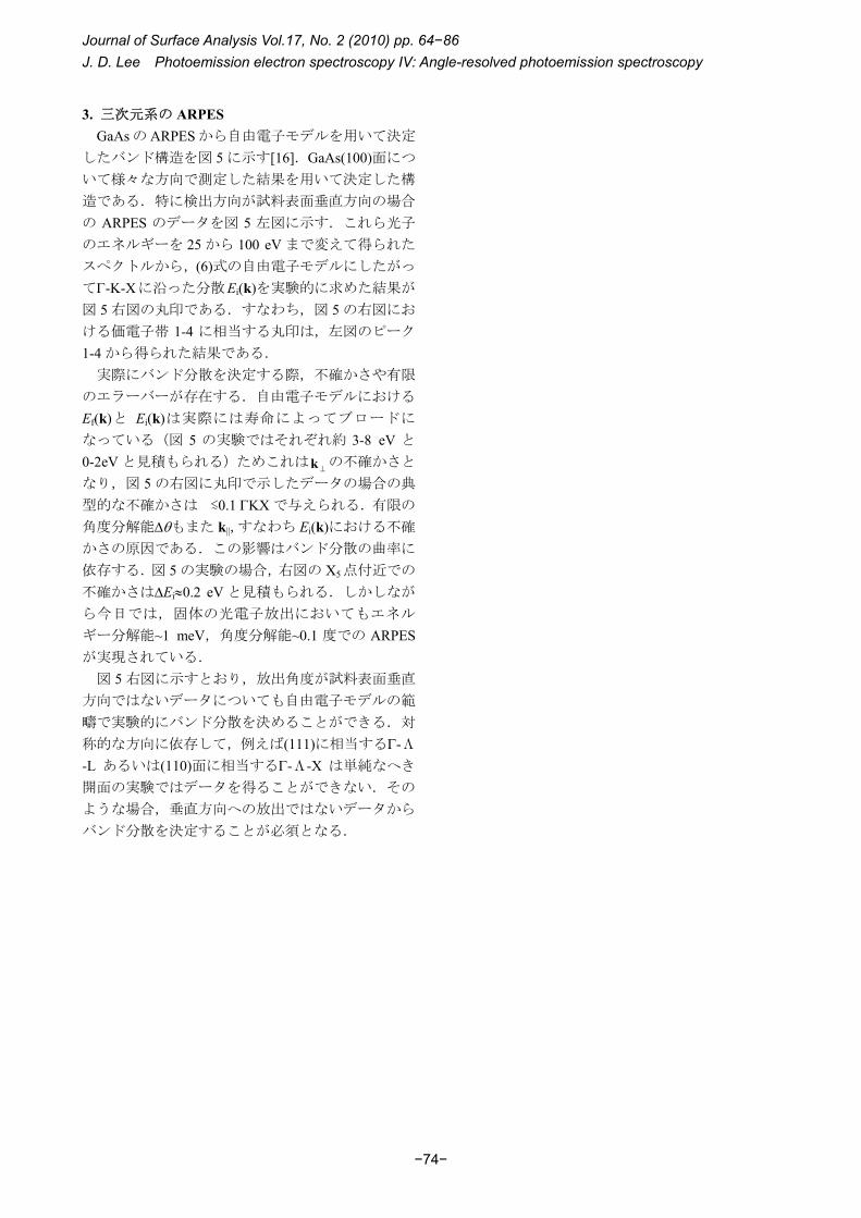
Finally, in Fig.6, we provide another example of high resolution ARPES for the narrow band materials (e.g., transition metals with d bands) [17]. The data are taken in the normal emission from different crystal faces. The d band of Ni attracts much theoretical and experimental interest since they are associated with the chemical reac-tivity of transition metal surfaces.
Fig. 6. Experimental energy band dispersion for Ni obtained from the normal emission data using different crystal faces. Comparing to the theoretical calculation [18], it is found that some bands do not appear in the experimental bands because they are forbidden by the selection rule of the dipole transition. The figure is taken from Ref. [17].
4. ARPES of low-dimensional systems As mentioned previously, the ultimate merit and fruit-
fulness of ARPES can be found in the study for the low-dimensional (one- or two-dimensional) systems. Many intriguing systems in both respects of science and application belong to the low-dimensional electron sys-tems. Among those, the most important would be proba-bly the high Tc superconductors, where the electronic conduction occurs in the two-dimensional CuO2 plane. Another interesting system might be graphite or gra-phene, a quasi-two-dimensional or two-dimensional hexagonal carbon layer. The one-dimensional electron system is also very interesting because the electron cor-relation used to make dramatic effects which are not ob-
served in higher dimensions, which could be directly visualized by ARPES.
4.1. High Tc superconductors
The discovery of superconductivity in the LaBaCuO ceramics by Bednorz and Müller [19] starts the race of high Tc superconductors. Intense activities are prompted in the field of ceramic oxides and compounds with in-creasingly higher Tc have shown up. Importantly, all the compounds are characterized by a layered crystal struc-ture with one or more CuO2 planes per unit cell, and a quasi-two-dimensional electronic structure.
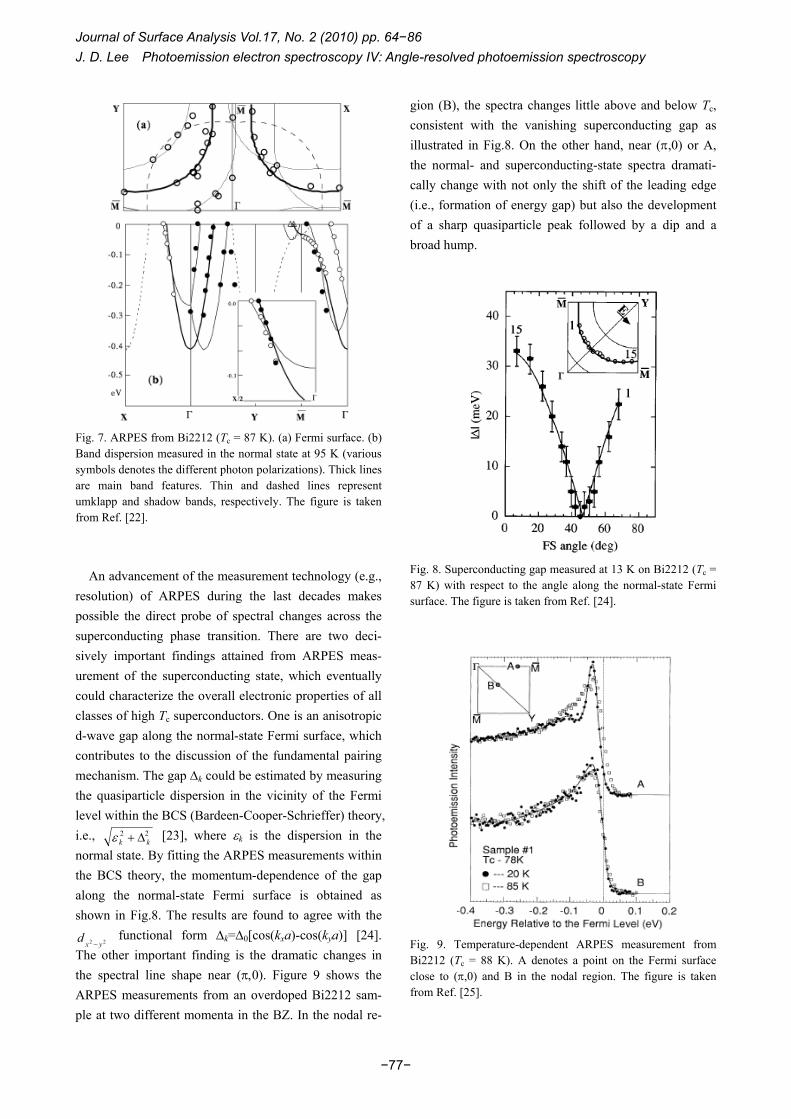
Among high Tc superconductors, the most intensively investigated one is Bi2Sr2CaCu2O8+δ (Bi2212) owing to the availability of large high quality single crystals. Here we introduce some beautiful ARPES studies concentrat-ing on Bi2212. The normal state (T > Tc) electronic properties would be studied firstly by the Fermi surface topology. But it has been a topic under controversy since the beginning of the investigation because of a few com-plications in addition to the primary band features. First, there are shadow bands, replicas of the main Fermi sur-face shifted by the wave vector (π,π) in the two-dimensional BZ [20]. Second, there are the umkalpp bands which are referred to as originating from the dif-fraction of the photoelectrons off the superstructure in the BiO layers [21]. Third, there is the so-called bilayer band splitting, that is, the coupling between two CuO2 planes in a unit cell of Bi2212 derives the electronic structure split into bonding and antibonding bands. The splitting is maximum at (π,0) and vanishes along the (0,0) – (π,π) direction. In Fig.7, the experimental Fermi surface shows these features.
Journal of Surface Analysis Vol.17, No. 2 (2010) pp. 64−86 J. D. Lee Photoemission electron spectroscopy IV: Angle-resolved photoemission spectroscopy
−76−
後に他の例として,狭バンド金属(例えば d バ
ンドをもつ遷移金属など)に対する高分解能 ARPESの例を示す[17].データは異なる結晶面に対して表
面垂直方向で測定した結果である.遷移金属の反応
活性に関連することからNiのdバンドは実験的にも
理論的にも大変注目されている系である.
4. 低次元系に対する AEPES 以前述べた通り,ARPES の突出した利点と有用さ
は低次元系(一次元あるいは二次元系)の研究にお
いて確認できる.科学あるいは実用の両方の観点で
興味深い多くの系は低次元電子系である.それらの
うち も重要なのは,電気伝導が二次元の CuO2 面
で起きる高温超伝導体であろう.他に興味深い系は,
擬二次元,あるいは二次元の六方晶炭素層を持つグ
ラファイトやグラフェンである.一次元電子系もま
た電子相関が大きな影響を与える傾向があり大変興
味深く,この影響は高次元系では観測されず ARPESでのみ可視化できる.
4.1. 高温(Tc)超伝導体
Bednorz と Müller によってなされた LaBaCuO セ
ラミックにおける超電導現象の発見[19]は高温超伝
導体の競争の幕開けとなった.酸化物セラミックス
あるいは化合物の分野において超電導転移温度が上
昇するのに伴って研究活動が活発化した.重要なこ
とは,単位格子内に一つあるいはそれ以上の CuO2
面を持つ層状の結晶構造,すなわち擬二次元電子構
造によって全ての化合物が特徴付けられることであ
る. 高温超伝導体の中で も精力的に調べられたもの
は , 質 の 高 い 大 き な 単 結 晶 が 得 ら れ る
Bi2Sr2CaCu2O8+δ (Bi2212)である.ここで,Bi2212 に
関する見事な ARPES の研究のいくつかを紹介する.
常伝導状態(T>Tc,Tc は転移温度)での電子的特性
はフェルミ面の形状を通じて 初に調べるのが普通
であろう.しかしながら,これは基本的なバンド構
造の特徴に加えていくつかの複雑さのために議論の
分かれるトピックであった.複雑さの一つ目が
shadow バンドであり,これは主たるフェルミ面を二
次元ブリルアンゾーンにおいて波数(π,π)だけシフト
したレプリカである[20].次が umkalpp バンドで,
これはBiO層にある超構造からはずれて行く光電子
回折に起因すると考えられている[21].3 番目にいわ
ゆる二重層バンド分離,すなわち Bi2212 単位格子内
の 2 つの CuO2 層の間のカップリングによって電子
状態が結合状態と反結合状態へ分離することがある.
分離は(π,0)で 大であり,(0,0) – (π,π)方向で見られ
なくなる.図 7 に示した実験的に得られたフェルミ
面では,これらの特徴が確認できる.
Journal of Surface Analysis Vol.17, No. 2 (2010) pp. 64−86 J. D. Lee Photoemission electron spectroscopy IV: Angle-resolved photoemission spectroscopy
−77−
Fig. 7. ARPES from Bi2212 (Tc = 87 K). (a) Fermi surface. (b) Band dispersion measured in the normal state at 95 K (various symbols denotes the different photon polarizations). Thick lines are main band features. Thin and dashed lines represent umklapp and shadow bands, respectively. The figure is taken from Ref. [22].
An advancement of the measurement technology (e.g.,
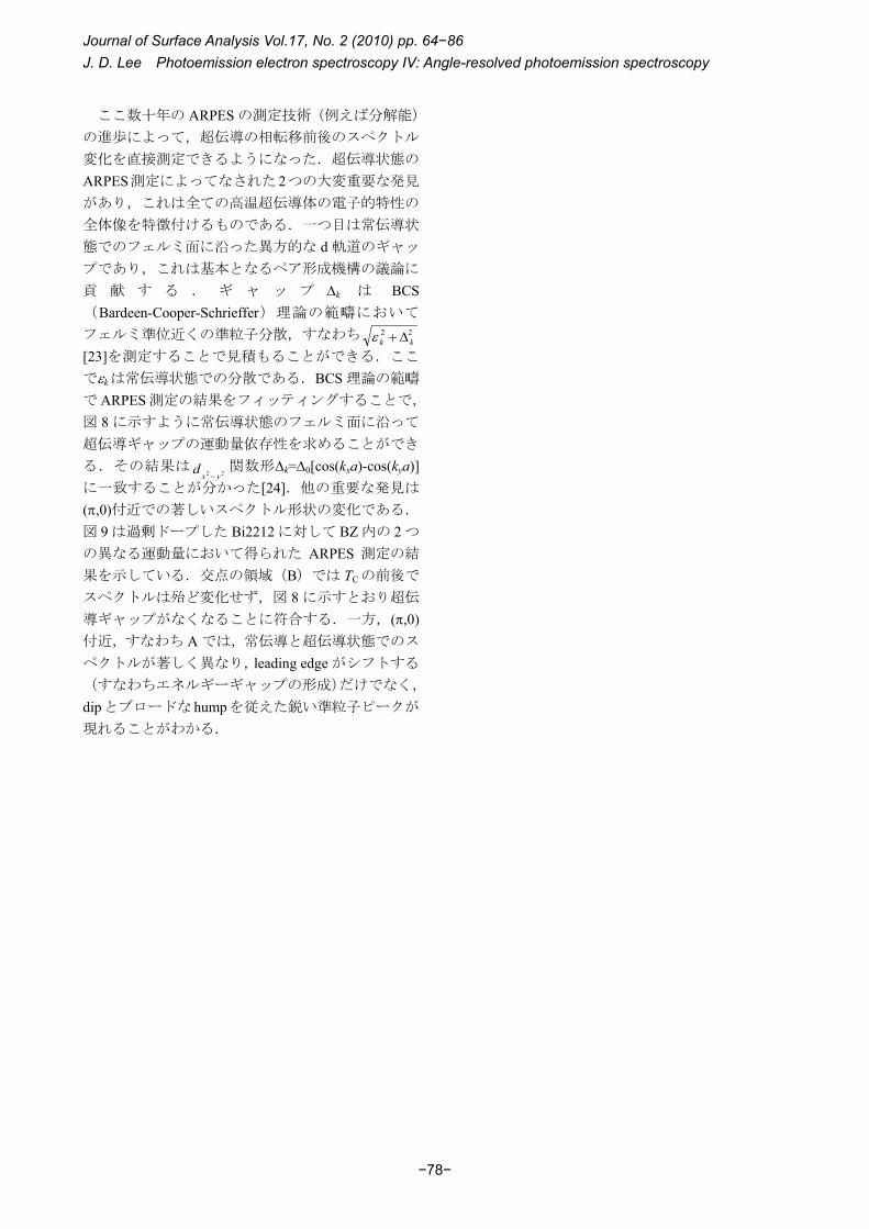
resolution) of ARPES during the last decades makes possible the direct probe of spectral changes across the superconducting phase transition. There are two deci-sively important findings attained from ARPES meas-urement of the superconducting state, which eventually could characterize the overall electronic properties of all classes of high Tc superconductors. One is an anisotropic d-wave gap along the normal-state Fermi surface, which contributes to the discussion of the fundamental pairing mechanism. The gap Δk could be estimated by measuring the quasiparticle dispersion in the vicinity of the Fermi level within the BCS (Bardeen-Cooper-Schrieffer) theory, i.e., 22
kk Δ+ε [23], where εk is the dispersion in the normal state. By fitting the ARPES measurements within the BCS theory, the momentum-dependence of the gap along the normal-state Fermi surface is obtained as shown in Fig.8. The results are found to agree with the
22 yxd
− functional form Δk=Δ0[cos(kxa)-cos(kya)] [24].
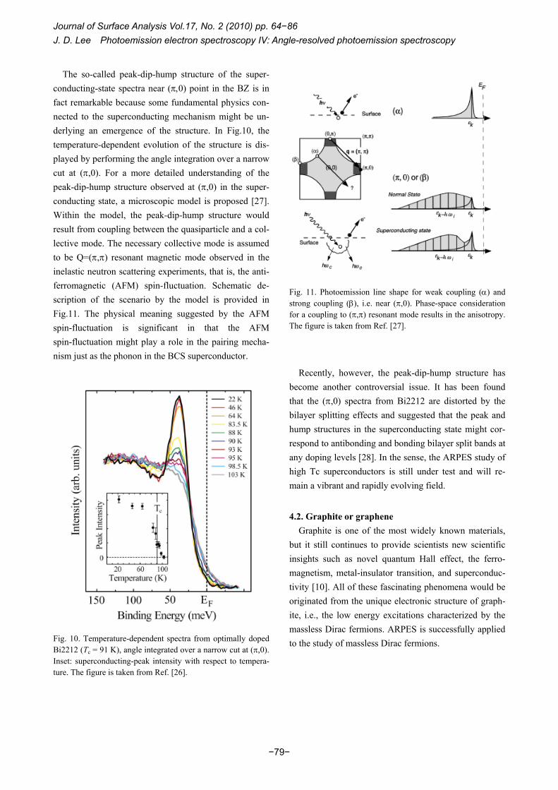
The other important finding is the dramatic changes in the spectral line shape near (π,0). Figure 9 shows the ARPES measurements from an overdoped Bi2212 sam-ple at two different momenta in the BZ. In the nodal re-
gion (B), the spectra changes little above and below Tc, consistent with the vanishing superconducting gap as illustrated in Fig.8. On the other hand, near (π,0) or A, the normal- and superconducting-state spectra dramati-cally change with not only the shift of the leading edge (i.e., formation of energy gap) but also the development of a sharp quasiparticle peak followed by a dip and a broad hump.
Fig. 8. Superconducting gap measured at 13 K on Bi2212 (Tc = 87 K) with respect to the angle along the normal-state Fermi surface. The figure is taken from Ref. [24].
Fig. 9. Temperature-dependent ARPES measurement from Bi2212 (Tc = 88 K). A denotes a point on the Fermi surface close to (π,0) and B in the nodal region. The figure is taken from Ref. [25].
Journal of Surface Analysis Vol.17, No. 2 (2010) pp. 64−86 J. D. Lee Photoemission electron spectroscopy IV: Angle-resolved photoemission spectroscopy
−78−
ここ数十年の ARPES の測定技術(例えば分解能)
の進歩によって,超伝導の相転移前後のスペクトル
変化を直接測定できるようになった.超伝導状態の
ARPES測定によってなされた2つの大変重要な発見
があり,これは全ての高温超伝導体の電子的特性の
全体像を特徴付けるものである.一つ目は常伝導状
態でのフェルミ面に沿った異方的な d 軌道のギャッ
プであり,これは基本となるペア形成機構の議論に
貢 献 す る . ギ ャ ッ プ Δk は BCS(Bardeen-Cooper-Schrieffer)理論の範疇において
フェルミ準位近くの準粒子分散,すなわち 22kk Δ+ε
[23]を測定することで見積もることができる.ここ
でεkは常伝導状態での分散である.BCS 理論の範疇
で ARPES 測定の結果をフィッティングすることで,
図 8 に示すように常伝導状態のフェルミ面に沿って
超伝導ギャップの運動量依存性を求めることができ
る.その結果は22 yx
d−
関数形Δk=Δ0[cos(kxa)-cos(kya)]に一致することが分かった[24].他の重要な発見は
(π,0)付近での著しいスペクトル形状の変化である.
図 9 は過剰ドープした Bi2212 に対して BZ 内の 2 つ
の異なる運動量において得られた ARPES 測定の結
果を示している.交点の領域(B)では TCの前後で
スペクトルは殆ど変化せず,図 8 に示すとおり超伝
導ギャップがなくなることに符合する.一方,(π,0)付近,すなわち A では,常伝導と超伝導状態でのス
ペクトルが著しく異なり,leading edge がシフトする
(すなわちエネルギーギャップの形成)だけでなく,
dipとブロードな humpを従えた鋭い準粒子ピークが
現れることがわかる.
Journal of Surface Analysis Vol.17, No. 2 (2010) pp. 64−86 J. D. Lee Photoemission electron spectroscopy IV: Angle-resolved photoemission spectroscopy
−79−
The so-called peak-dip-hump structure of the super-conducting-state spectra near (π,0) point in the BZ is in fact remarkable because some fundamental physics con-nected to the superconducting mechanism might be un-derlying an emergence of the structure. In Fig.10, the temperature-dependent evolution of the structure is dis-played by performing the angle integration over a narrow cut at (π,0). For a more detailed understanding of the peak-dip-hump structure observed at (π,0) in the super-conducting state, a microscopic model is proposed [27]. Within the model, the peak-dip-hump structure would result from coupling between the quasiparticle and a col-lective mode. The necessary collective mode is assumed to be Q=(π,π) resonant magnetic mode observed in the inelastic neutron scattering experiments, that is, the anti-ferromagnetic (AFM) spin-fluctuation. Schematic de-scription of the scenario by the model is provided in Fig.11. The physical meaning suggested by the AFM spin-fluctuation is significant in that the AFM spin-fluctuation might play a role in the pairing mecha-nism just as the phonon in the BCS superconductor.
Fig. 10. Temperature-dependent spectra from optimally doped Bi2212 (Tc = 91 K), angle integrated over a narrow cut at (π,0). Inset: superconducting-peak intensity with respect to tempera-ture. The figure is taken from Ref. [26].
Fig. 11. Photoemission line shape for weak coupling (α) and strong coupling (β), i.e. near (π,0). Phase-space consideration for a coupling to (π,π) resonant mode results in the anisotropy. The figure is taken from Ref. [27].
Recently, however, the peak-dip-hump structure has become another controversial issue. It has been found that the (π,0) spectra from Bi2212 are distorted by the bilayer splitting effects and suggested that the peak and hump structures in the superconducting state might cor-respond to antibonding and bonding bilayer split bands at any doping levels [28]. In the sense, the ARPES study of high Tc superconductors is still under test and will re-main a vibrant and rapidly evolving field.
4.2. Graphite or graphene Graphite is one of the most widely known materials,
but it still continues to provide scientists new scientific insights such as novel quantum Hall effect, the ferro-magnetism, metal-insulator transition, and superconduc-tivity [10]. All of these fascinating phenomena would be originated from the unique electronic structure of graph-ite, i.e., the low energy excitations characterized by the massless Dirac fermions. ARPES is successfully applied to the study of massless Dirac fermions.
Journal of Surface Analysis Vol.17, No. 2 (2010) pp. 64−86 J. D. Lee Photoemission electron spectroscopy IV: Angle-resolved photoemission spectroscopy
−80−
BZ の(π,0)点付近の超伝導状態のスペクトルに見
られるいわゆる peak-dip-hump 構造は実際に顕著で
あり,これは,超伝導現象に関連する基礎的な物理
の背景がこの構造が出現することにあるためである.
図 10 は,この構造の温度依存性を示しており,(π,0)での狭い範囲を角度積分した結果である.超伝導状
態の(π,0)で観測される peak-dip-hump 構造をより詳
しく理解するために,微視的なモデルが提案されて
いる[27].このモデルでは,peak-dip-hump 構造は準
粒子と集団モードの相互作用として説明される.必
要となる集団モードは,非弾性中性子散乱測定で観
測される共鳴磁気モード Q=(π,π),すなわち,反強
磁性(AFM)スピン揺らぎと仮定する.このモデル
によるシナリオの模式図を図 11 に示す.AFM スピ
ン揺らぎによって提案される物理的意味は,BCS 超
伝導体におけるフォノンのように,AFM スピン揺ら
ぎがペアを形成する機構において有用な役割を果た
す点で顕著である. しかしながら,近年 peak-dip-hump 構造は他の議
論の的となっている.Bi2212 の(π,0)スペクトルが二
重層分離効果によって乱されることが見出され,超
伝導状態での peak-hump 構造がいかなるドープレベ
ルにおいても反結合及び結合二重層分離バンドに相
当するのではないかと提案された[28].この意味で,
高温超伝導体に関する ARPES を用いた研究は未だ
試行錯誤の段階であり,今後も興味深く急激に進展
する研究分野であるといえる.
4.2. グラファイトとグラフェン グラファイトは も広く知られた物質の一つであ
るが,新しい量子ホール効果や強磁性,金属-絶縁
体転移,超伝導など,新しい科学的発見が続いてい
る材料である[10].これら全ての興味深い現象はグ
ラファイトに唯一の特徴的な電子構造,すなわち,
質量の無いディラックフェルミオンによって特徴付
けられる低エネルギー励起に起因する.ARPES は質
量の無いディラックフェルミオンの研究に応用され
成功している.
Journal of Surface Analysis Vol.17, No. 2 (2010) pp. 64−86 J. D. Lee Photoemission electron spectroscopy IV: Angle-resolved photoemission spectroscopy
−81−
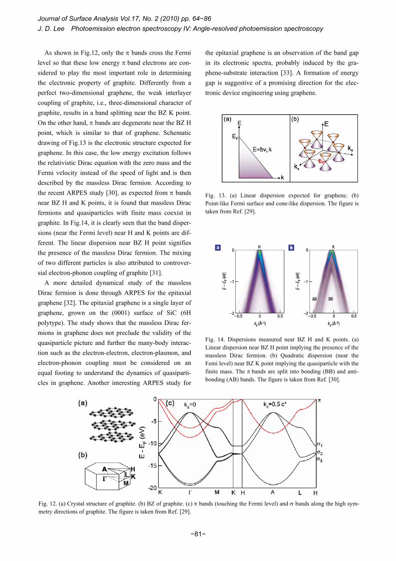
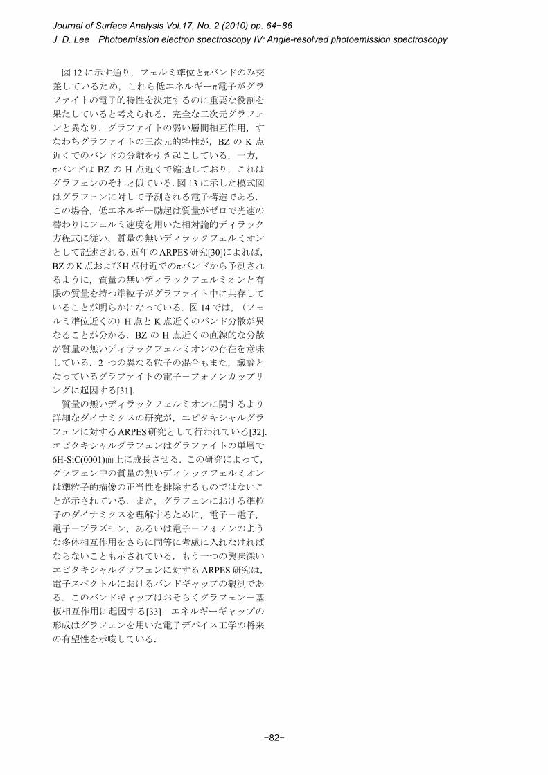
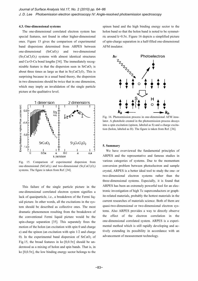
As shown in Fig.12, only the π bands cross the Fermi level so that these low energy π band electrons are con-sidered to play the most important role in determining the electronic property of graphite. Differently from a perfect two-dimensional graphene, the weak interlayer coupling of graphite, i.e., three-dimensional character of graphite, results in a band splitting near the BZ K point. On the other hand, π bands are degenerate near the BZ H point, which is similar to that of graphene. Schematic drawing of Fig.13 is the electronic structure expected for graphene. In this case, the low energy excitation follows the relativistic Dirac equation with the zero mass and the Fermi velocity instead of the speed of light and is then described by the massless Dirac fermion. According to the recent ARPES study [30], as expected from π bands near BZ H and K points, it is found that massless Dirac fermions and quasiparticles with finite mass coexist in graphite. In Fig.14, it is clearly seen that the band disper-sions (near the Fermi level) near H and K points are dif-ferent. The linear dispersion near BZ H point signifies the presence of the massless Dirac fermion. The mixing of two different particles is also attributed to controver-sial electron-phonon coupling of graphite [31].
A more detailed dynamical study of the massless Dirac fermion is done through ARPES for the epitaxial graphene [32]. The epitaxial graphene is a single layer of graphene, grown on the (0001) surface of SiC (6H polytype). The study shows that the massless Dirac fer-mions in graphene does not preclude the validity of the quasiparticle picture and further the many-body interac-tion such as the electron-electron, electron-plasmon, and electron-phonon coupling must be considered on an equal footing to understand the dynamics of quasiparti-cles in graphene. Another interesting ARPES study for
the epitaxial graphene is an observation of the band gap in its electronic spectra, probably induced by the gra-phene-substrate interaction [33]. A formation of energy gap is suggestive of a promising direction for the elec-tronic device engineering using graphene.
Fig. 13. (a) Linear dispersion expected for graphene. (b) Point-like Fermi surface and cone-like dispersion. The figure is taken from Ref. [29].
Fig. 14. Dispersions measured near BZ H and K points. (a) Linear dispersion near BZ H point implying the presence of the massless Dirac fermion. (b) Quadratic dispersion (near the Femi level) near BZ K point implying the quasiparticle with the finite mass. The π bands are split into bonding (BB) and anti-bonding (AB) bands. The figure is taken from Ref. [30].
Fig. 12. (a) Crystal structure of graphite. (b) BZ of graphite. (c) π bands (touching the Fermi level) and σ bands along the high sym-metry directions of graphite. The figure is taken from Ref. [29].
Journal of Surface Analysis Vol.17, No. 2 (2010) pp. 64−86 J. D. Lee Photoemission electron spectroscopy IV: Angle-resolved photoemission spectroscopy
−82−
図 12 に示す通り,フェルミ準位とπバンドのみ交
差しているため,これら低エネルギーπ電子がグラ
ファイトの電子的特性を決定するのに重要な役割を
果たしていると考えられる.完全な二次元グラフェ
ンと異なり,グラファイトの弱い層間相互作用,す
なわちグラファイトの三次元的特性が,BZ の K 点
近くでのバンドの分離を引き起こしている.一方,
πバンドは BZ の H 点近くで縮退しており,これは
グラフェンのそれと似ている.図 13 に示した模式図
はグラフェンに対して予測される電子構造である.
この場合,低エネルギー励起は質量がゼロで光速の
替わりにフェルミ速度を用いた相対論的ディラック
方程式に従い,質量の無いディラックフェルミオン
として記述される.近年のARPES研究[30]によれば,
BZのK点およびH点付近でのπバンドから予測され
るように,質量の無いディラックフェルミオンと有
限の質量を持つ準粒子がグラファイト中に共存して
いることが明らかになっている.図 14 では,(フェ
ルミ準位近くの)H 点と K 点近くのバンド分散が異
なることが分かる.BZ の H 点近くの直線的な分散
が質量の無いディラックフェルミオンの存在を意味
している.2 つの異なる粒子の混合もまた,議論と
なっているグラファイトの電子-フォノンカップリ
ングに起因する[31]. 質量の無いディラックフェルミオンに関するより
詳細なダイナミクスの研究が,エピタキシャルグラ
フェンに対するARPES研究として行われている[32].エピタキシャルグラフェンはグラファイトの単層で
6H-SiC(0001)面上に成長させる.この研究によって,
グラフェン中の質量の無いディラックフェルミオン
は準粒子的描像の正当性を排除するものではないこ
とが示されている.また,グラフェンにおける準粒
子のダイナミクスを理解するために,電子-電子,
電子-プラズモン,あるいは電子-フォノンのよう
な多体相互作用をさらに同等に考慮に入れなければ
ならないことも示されている.もう一つの興味深い
エピタキシャルグラフェンに対する ARPES 研究は,
電子スペクトルにおけるバンドギャップの観測であ
る.このバンドギャップはおそらくグラフェン-基
板相互作用に起因する[33].エネルギーギャップの
形成はグラフェンを用いた電子デバイス工学の将来
の有望性を示唆している.
Journal of Surface Analysis Vol.17, No. 2 (2010) pp. 64−86 J. D. Lee Photoemission electron spectroscopy IV: Angle-resolved photoemission spectroscopy
−83−
4.3. One-dimensional systems The one-dimensional correlated electron system has
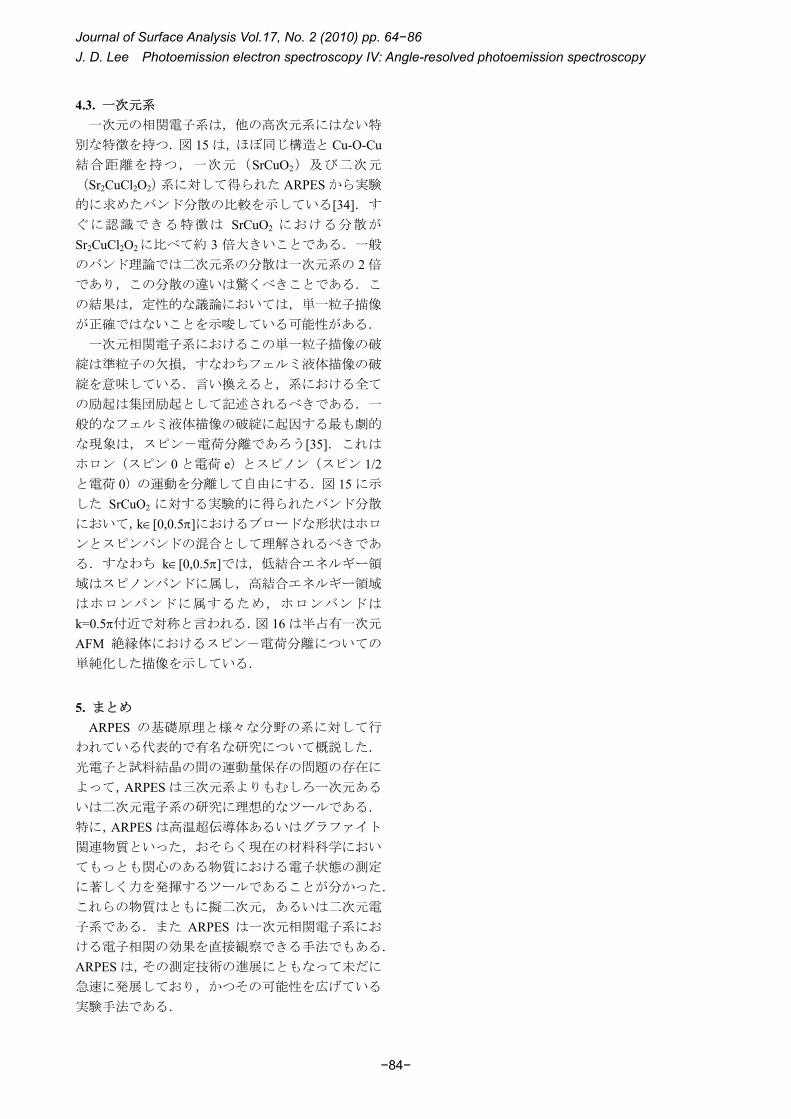
special features, not found in other higher-dimensional ones. Figure 15 gives the comparison of experimental band dispersions determined from ARPES between one-dimensional (SrCuO2) and two-dimensional (Sr2CuCl2O2) systems with almost identical structures and Cu-O-Cu bond lengths [34]. The immediately recog-nizable feature is that the dispersion seen in SrCuO2 is about three times as large as that in Sr2CuCl2O2. This is surprising because in a usual band theory, the dispersion in two dimensions should be twice that in one dimension, which may imply an invalidation of the single particle picture at the qualitative level.
Fig. 15. Comparison of experimental dispersion from one-dimensional (SrCuO2) and two-dimensional (Sr2CuCl2O2) systems. The figure is taken from Ref. [34].
This failure of the single particle picture in the one-dimensional correlated electron system signifies a lack of quasiparticle, i.e., a breakdown of the Fermi liq-uid picture. In other words, all the excitations in the sys-tem should be described as collective ones. The most dramatic phenomenon resulting from the breakdown of the conventional Fermi liquid picture would be the spin-charge separation [35]. This separately frees the motion of the holon (an excitation with spin 0 and charge e) and the spinon (an excitation with spin 1/2 and charge 0). In the experimental band dispersion of SrCuO2 of Fig.15, the broad features in k∈[0,0.5π] should be un-derstood as a mixing of holon and spin bands. That is, in k∈[0,0.5π], the low binding energy sector belongs to the
spinon band and the high binding energy sector to the holon band so that the holon band is noted to be symmet-ric around k=0.5π. Figure 16 depicts a simplified picture of spin-charge separation in a half-filled one-dimensional AFM insulator.
Fig. 16. Photoemission process in one-dimensional AFM insu-lator. A photohole created in the photoemission process decays into a spin excitation (spinon, labeled as S) and a charge excita-tion (holon, labeled as H). The figure is taken from Ref. [36].
5. Summary We have overviewed the fundamental principles of
ARPES and the representative and famous studies in various categories of systems. Due to the momentum conversion problem between photoelectron and sample crystal, ARPES is a better ideal tool to study the one- or two-dimensional electron systems rather than the three-dimensional systems. Especially, it is found that ARPES has been an extremely powerful tool for an elec-tronic investigation of high Tc superconductors or graph-ite-related materials, probably the hottest materials in the current researches of materials science. Both of them are quasi-two-dimensional or two-dimensional electron sys-tems. Also ARPES provides a way to directly observe the effect of the electron correlation in the one-dimensional correlated system. ARPES is a experi-mental method which is still rapidly developing and ac-tively extending its possibility in accordance with an advancement of measurement technology.
Journal of Surface Analysis Vol.17, No. 2 (2010) pp. 64−86 J. D. Lee Photoemission electron spectroscopy IV: Angle-resolved photoemission spectroscopy
−84−
4.3. 一次元系 一次元の相関電子系は,他の高次元系にはない特
別な特徴を持つ.図 15 は,ほぼ同じ構造と Cu-O-Cu結合距離を持つ,一次元(SrCuO2)及び二次元
(Sr2CuCl2O2)系に対して得られた ARPES から実験
的に求めたバンド分散の比較を示している[34].す
ぐに認識できる特徴は SrCuO2 における分散が
Sr2CuCl2O2に比べて約 3 倍大きいことである.一般
のバンド理論では二次元系の分散は一次元系の 2 倍
であり,この分散の違いは驚くべきことである.こ
の結果は,定性的な議論においては,単一粒子描像
が正確ではないことを示唆している可能性がある. 一次元相関電子系におけるこの単一粒子描像の破
綻は準粒子の欠損,すなわちフェルミ液体描像の破
綻を意味している.言い換えると,系における全て
の励起は集団励起として記述されるべきである.一
般的なフェルミ液体描像の破綻に起因する も劇的
な現象は,スピン-電荷分離であろう[35].これは
ホロン(スピン 0 と電荷 e)とスピノン(スピン 1/2と電荷 0)の運動を分離して自由にする.図 15 に示
した SrCuO2 に対する実験的に得られたバンド分散
において,k∈[0,0.5π]におけるブロードな形状はホロ
ンとスピンバンドの混合として理解されるべきであ
る.すなわち k∈[0,0.5π]では,低結合エネルギー領
域はスピノンバンドに属し,高結合エネルギー領域
はホロンバンドに属するため,ホロンバンドは
k=0.5π付近で対称と言われる.図 16 は半占有一次元
AFM 絶縁体におけるスピン-電荷分離についての
単純化した描像を示している.
5. まとめ ARPES の基礎原理と様々な分野の系に対して行
われている代表的で有名な研究について概説した.
光電子と試料結晶の間の運動量保存の問題の存在に
よって,ARPES は三次元系よりもむしろ一次元ある
いは二次元電子系の研究に理想的なツールである.
特に,ARPES は高温超伝導体あるいはグラファイト
関連物質といった,おそらく現在の材料科学におい
てもっとも関心のある物質における電子状態の測定
に著しく力を発揮するツールであることが分かった.
これらの物質はともに擬二次元,あるいは二次元電
子系である.また ARPES は一次元相関電子系にお
ける電子相関の効果を直接観察できる手法でもある.
ARPES は,その測定技術の進展にともなって未だに
急速に発展しており,かつその可能性を広げている
実験手法である.
Journal of Surface Analysis Vol.17, No. 2 (2010) pp. 64−86 J. D. Lee Photoemission electron spectroscopy IV: Angle-resolved photoemission spectroscopy
−85−
6. Acknowledgment We acknowledge Prof. Goro Mizutani for encouraging
this review work on the photoemission electron spec-troscopy. This manuscript was prepared during the visit to Max-Planck Institute für Quantenoptik (MPQ) in Garching, Germany. We are grateful to MPQ for the hospitality and support. This work was supported by Special Coordination Funds for Promoting Science and Technology from MEXT, Japan.
6. 謝辞 光電子分光に関する本原稿の執筆にご協力いただ
いた Prof. Goro Mizutani に感謝いたします.本稿は,
Max-Planck Institute für Quantenoptik (MPQ) in Garching 滞在中に執筆したものであり,MPQ の厚遇
と補助に感謝いたします.本稿は文部科学省からの
補助をもとに執筆いたしました.
Journal of Surface Analysis Vol.17, No. 2 (2010) pp. 64−86 J. D. Lee Photoemission electron spectroscopy IV: Angle-resolved photoemission spectroscopy
−86−
7. References [1] J. D. Lee, J. Surf. Anal. 16, 42 (2009). [2] J. D. Lee, J. Surf. Anal. 16, 127 (2009). [3] J. D. Lee, J. Surf. Anal. 16, 196 (2010). [4] L. Ley and M. Cardona, Photoemission in solids, vol.
II (Springer-Verlag, Berlin, 1979). [5] N. V. Smith and F. J. Himpsel, in Handbook on Syn-
chrotron Radiation, ed. by E. E. Koch (North-Holland, Amsterdam, 1983).
[6] S. Hüfner, Photoelectron spectroscopy (Springer-Verlag, Berlin, 2003).
[7] A. Damascelli, Physica Scripta T109, 61 (2004). [8] G. D. Mahan, Many-Particle Physics (Plenum, New
York, 1981). [9] A. Damascelli, Z. Hussain, and Z.-X. Shen, Rev. Mod.
Phys. 75, 473 (2003). [10] A. H. Castro Neto, F. Guinea, N. M. R. Peres, K. S.
Novoselov, and A. K. Geim, Rev. Mod. Phys. 81, 109 (2009).
[11] As a matter of fact, Eq.(2) would be valid in the one- or two-dimensional systems, but not always in the three-dimensional ones because of an absence of a simple relation between photoelectron mo-mentum and crystal momentum.
[12] F. J. Himpsel, Appl. Opt. 19, 3964 (1980). [13] H. Mårtensson and P. O. Nilsson, Phys. Rev. B 30,
3047 (1984). [14] D. Kane, Phys. Rev. Lett. 12, 97 (1964). [15] E. Dietz, H. Becker, and U. Gerhardt, Phys. Rev.
Lett. 36, 1397 (1976). [16] T. C. Chiang, J. A. Knapp, M. Aono, and D. E.
Eastman, Phys. Rev. B 21, 3513 (1980). [17] F. J. Himpsel, J. A. Knapp, and D. E. Eastman, Phys.
Rev. B 19, 2919 (1979). [18] V. L. Moruzzi, J. F. Janak, and A. R. Williams, Cal-
culated Electron Properties of Metals (Pergamon, New York, 1978).
[19] J. G. Bednorz and K. A. Müller, Z. Phys. B: Con-dens. Matter 64, 189 (1986).
[20] P. Aebi, J. Osterwalder, P. Schwaller, L. Schlapbach, M. Shimoda, T. Mochiku, and K. Kadowaki, Phys. Rev. Lett. 72, 2757 (1994).
[21] P. Aebi, J. Osterwalder, P. Schwaller, H. Berger, C. Beeli, and L. Schlapbach, J. Phys. Chem. Solids 56, 1845 (1995).
[22] H. Ding, A. F. Bellman, J. C. Campuzano, M.
Randeria, M. R. Norman, T. Yokoya, T. Takahashi, H. Katayama-Yoshida, T. Mochiku, K. Kadowaki, G. Jennings, and G.P. Brivio, Phys. Rev. Lett. 76, 1533 (1996).
[23] J. R. Schrieffer, Theory of superconductivity (Addi-son-Wesley, New York, 1964).
[24] H. Ding, M. R. Norman, J. C. Campuzano, M. Randeria, A. F. Bellman, T. Yokoya, T. Takahashi, T. Mochiku, and K. Kadowaki, Phys. Rev. B 54, 9678 (1996).
[25] Z.-X. Shen, D. S. Dessau, B. O. Wells, D. M. King, W. E. Spicer, A. J. Arko, D. Marshall, L. W. Lombardo, A. Kapitulnik, P. Dickinson, J. DiCarlo, T. Loeser, and C. H. Park, Phys. Rev. Lett. 70, 1553 (1993).
[26] A. Fedorov, V. T. Valla, P. D. Johnson, Q. Li, G. D. Gu, and N. Koshizuka, Phys. Rev. Lett. 82, 2179 (1999).
[27] Z.-X. Shen and J. R. Schrieffer, Phys. Rev. Lett. 78, 1771 (1997).
[28] A. A. Kordyuk, S. V. Borisenko, T. K. Kim, K. Nenkov, M. Knufer, M. S. Golden, J. Fink, H. Berger, and R. Follath, Phys. Rev. Lett. 89, 077003 (2002).
[29] S. Y. Zhou, G. H. Gweon, and A. Lanzara, Ann. Phys. 321, 1730 (2006).
[30] S. Y. Zhou, G. H. Gweon, J. Graf, A. V. Fedorov, C. D. Spataru, R. D. Diehl, Y. Kopelevich, D. H. Lee, S. G. Louie, and A. Lanzara, Nature Phys. 2, 595 (2006).
[31] J. D. Lee, S. W. Han, and J. Inoue, Phys. Rev. Lett. 100, 216801 (2008).
[32] A. Bostwick, T. Ohta, T. Seyller, K. Horn, and E. Rotenberg, Nature Phys. 3, 36 (2007).
[33] S. Y. Zhou, G. H. Gweon, A. V. Fedorov, P. N. First, W. A. De Heer, D. H. Lee, F. Guinea, A. H. Castro Neto, and A. Lanzara, Nature Mater. 6, 770 (2007).
[34] C. Kim, A.Y. Matsuura, Z.-X. Shen, N. Motoyama, H. Eisaki, S. Uchida, T. Tohyama, and S. Maekawa, Phys. Rev. Lett. 77, 4054 (1996).
[35] E. H. Lieb and F. Y. Wu, Phys. Rev. Lett. 20, 1445 (1968).
[36] C. Kim, Z.-X. Shen, N. Motoyama, H. Eisaki, S. Uchida, T. Tohyama, and S. Maekawa, Phys. Rev. B 56, 15589 (1997).