
Advanced Information Storage 15 - University of Yorkah566/lectures/adv15_feram.pdf · Advanced...
11
Department of Electronics Advanced Information Storage 15 Atsufumi Hirohata 16:00 21/November/2013 Thursday (V 120) Quick Review over the Last Lecture MRAM read-out : Bit line Sensing current Word line Parallel magnetisation ↓ Low resistant state “0” Magnetic free layer Magnetic pin layer Antiparallel magnetisation ↓ High resistant state “1” Selection transistor (MOSFET) Insulator / nonmagnet Magnetic tunnel / spin-valve junctions * http://www.wikipedia.org/; ** M. Oogane and T. Miyazaki, “Magnetic Random Access Memory,” in Epitaxial Ferromagnetic Films and Spintronic Applications, A. Hirohata and Y. Otani (Eds.) (Research Signpost, Kerala, 2009) p. 335; MRAM STT write-in : *** http://www.toshiba.co.jp/ Perpendicularly magnetised MRAM :
Transcript of Advanced Information Storage 15 - University of Yorkah566/lectures/adv15_feram.pdf · Advanced...

1
Department of Electronics
Advanced Information Storage 15
Atsufumi Hirohata
16:00 21/November/2013 Thursday (V 120)
Quick Review over the Last Lecture
MRAM read-out :
Bit line Sensing current
Word line
Parallel magnetisation ↓
Low resistant state “0”
Magnetic free layer
Magnetic pin layer
Antiparallel magnetisation ↓
High resistant state “1”
Selection transistor (MOSFET)
Insulator / nonmagnet
Magnetic tunnel / spin-valve junctions
* http://www.wikipedia.org/;
** M. Oogane and T. Miyazaki, “Magnetic Random Access Memory,” in Epitaxial Ferromagnetic Films and Spintronic Applications, A. Hirohata and Y. Otani (Eds.) (Research Signpost, Kerala, 2009) p. 335;
MRAM STT write-in :
*** http://www.toshiba.co.jp/
Perpendicularly magnetised MRAM :

2
15 Ferroelectric / Phase Change Random Access Memory
• FeRAM
• PRAM
• ReRAM
Memory Types
* http://www.semiconductorjapan.net/serial/lesson/12.html
Rewritable�
Read only�
Read majority
(Writable) �
Volatile�
Non-volatile�
Non-volatile�
Non-volatile�
Dynamic �
Static �
Static �
Static �
Static �
DRAM�
SRAM�
MRAM�
FeRAM �
PRAM�
PROM�
Mask ROM�
Flash�
EPROM�

3
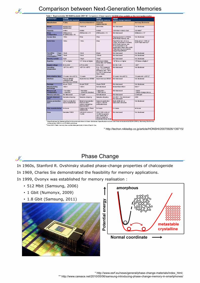
Comparison between Next-Generation Memories
* http://techon.nikkeibp.co.jp/article/HONSHI/20070926/139715/
Ferroelectric Random Access Memory (FeRAM)
* http://www.DudleyBuck.com/;
In 1952, Dudley A. Buck invented ferroelectric RAM in his master’s thesis :
** http://www.wikipedia.org/
Utilise ferroelectric polarisations
Very fast latency : < 1 ns
CMOS process compatible�
× Relatively large cell size : 15 F 2
× Destructive read-out

4
FeRAM Cells 1
* http://loto.sourceforge.net/feram/doc/film.xhtml
1-transistor 1-capacitor type : 1-transistor type :
FeRAM Cells 2
* http://www,wikipedia.org/
2-transistor 2-capacitor type :
Bit line 1 Bit line 2 Word line
Plate line
Ferroelectric capacitor 1
Ferroelectric capacitor 2
Bit line 1
Bit line 2
Word line
Plate line
Capacitor V 1
Capacitor V 2
FeRAM Writing operation Reading operation
Prevent destructive read-out �
5
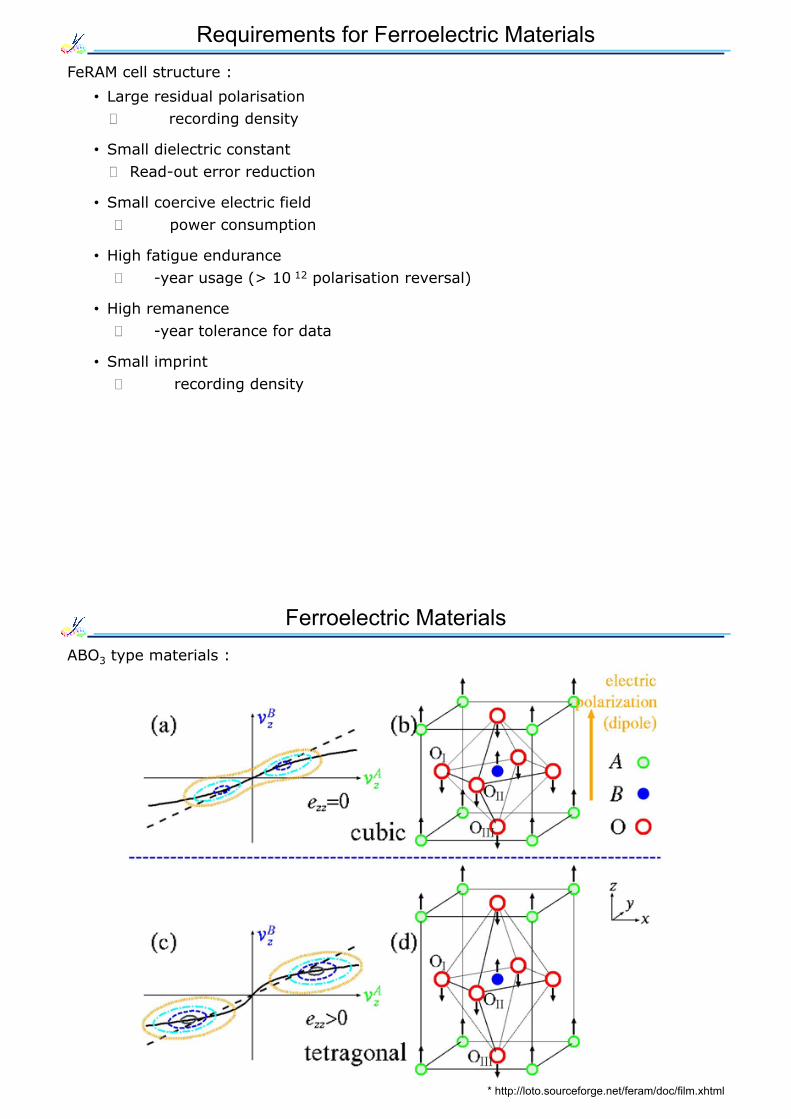
Requirements for Ferroelectric Materials FeRAM cell structure :
• Large residual polarisation → High recording density
• Small dielectric constant → Read-out error reduction
• Small coercive electric field → Low power consumption
• High fatigue endurance → 10-year usage (> 10 12 polarisation reversal)
• High remanence → 10-year tolerance for data
• Small imprint → High recording density
Ferroelectric Materials
* http://loto.sourceforge.net/feram/doc/film.xhtml
ABO3 type materials :

6
Polarisation Hysteresis
* http://loto.sourceforge.net/feram/doc/film.xhtml
For example, BaTiO3 :
Applications 2-Mb FeRAM introduced by Fujitsu :
* http://www.fujitsu.com/
7
Comparison between Next-Generation Memories
* http://techon.nikkeibp.co.jp/article/HONSHI/20070926/139715/
Phase Change In 1960s, Stanford R. Ovshinsky studied phase-change properties of chalcogenide
** http://www.careace.net/2010/05/06/samsung-introducing-phase-change-memory-in-smartphones/
In 1969, Charles Sie demonstrated the feasibility for memory applications.
In 1999, Ovonyx was established for memory realisation :
• 512 Mbit (Samsung, 2006)
• 1 Gbit (Numonyx, 2009)
• 1.8 Gbit (Samsung, 2011)
* http://www.esrf.eu/news/general/phase-change-materials/index_html;

8
Phase Change Random Access Memory (PRAM) Required writing currents for several techniques dependent upon cell size :
* http://www.wikipedia.org/;
Utilise phase change
Low resistivity : crystalline phase
High resistivity : amorphous phase
CMOS process compatible�
× Rewritability : 1,000 ~ 100,000 times
× Destructive read-out
http://nextgenlog.blogspot.com
PRAM Properties PRAM properties as compared with NOR-flash memory :
** http://www.hynix.com/mail/newsletter_2009_07/eng/sub02.html

9
PRAM Operation PRAM operation : *
* http://www.intechopen.com/books/advances-in-solid-state-circuit-technologies/impact-of-technology-scaling-on-phase-change-memory-performance
PRAM Architecture PRAM architecture : *
* http://www.intechopen.com/books/advances-in-solid-state-circuit-technologies/impact-of-technology-scaling-on-phase-change-memory-performance
10
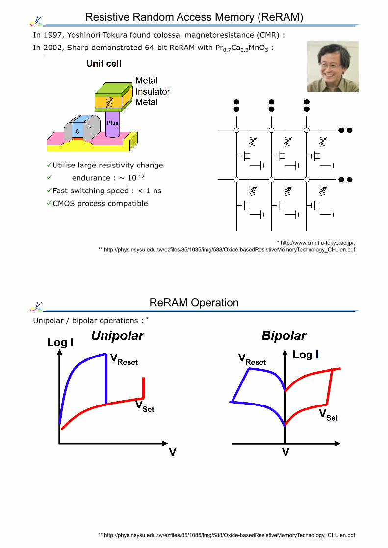
Resistive Random Access Memory (ReRAM) In 1997, Yoshinori Tokura found colossal magnetoresistance (CMR) :
* http://www.cmr.t.u-tokyo.ac.jp/;
In 2002, Sharp demonstrated 64-bit ReRAM with Pr0.7Ca0.3MnO3 :
** http://phys.nsysu.edu.tw/ezfiles/85/1085/img/588/Oxide-basedResistiveMemoryTechnology_CHLien.pdf
Utilise large resistivity change
High endurance : ~ 10 12
Fast switching speed : < 1 ns
CMOS process compatible�
ReRAM Operation Unipolar / bipolar operations : *
** http://phys.nsysu.edu.tw/ezfiles/85/1085/img/588/Oxide-basedResistiveMemoryTechnology_CHLien.pdf
11
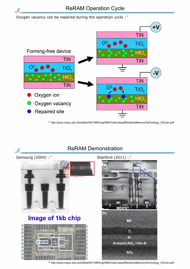
ReRAM Operation Cycle Oxygen vacancy can be repaired during the operation cycle : *
** http://phys.nsysu.edu.tw/ezfiles/85/1085/img/588/Oxide-basedResistiveMemoryTechnology_CHLien.pdf
ReRAM Demonstration Samsung (2004) : * Stanford (2011) : *
** http://phys.nsysu.edu.tw/ezfiles/85/1085/img/588/Oxide-basedResistiveMemoryTechnology_CHLien.pdf

![Software Resources for Remanence Estimation...Software Resources for Remanence Estimation Pratt, D.A.[1] 1. Tensor Research David.Pratt@tensor-research.com.au ABSTRACT The recovery](https://static.fdocuments.net/doc/165x107/606925cc3383eb5efc2d010c/software-resources-for-remanence-software-resources-for-remanence-estimation.jpg)


![Permanent magnets Ferrite, ndFeB, alniCo & smCo … · NdFeB BLS Magnet [6] Permanent magnets BLS Magnet [7] Permanent magnets nDFeB magnets Grade Remanence Remanence Coercive force](https://static.fdocuments.net/doc/165x107/5b915de509d3f210288b8282/permanent-magnets-ferrite-ndfeb-alnico-smco-ndfeb-bls-magnet-6-permanent.jpg)


