Addendum to FireStar Preliminary Data Book - opti … · (FireStar Preliminary Data Book PN...
158
Revision: 1.0 912-4000-013 October 3, 1997 OPTi ® FireStar Plus 64-Bit CPU Single Chip Notebook Solution Addendum to Preliminary Data Book (FireStar Preliminary Data Book PN 912-2000-015 Rev. 1.0) OPTi Confidential Preliminary
Transcript of Addendum to FireStar Preliminary Data Book - opti … · (FireStar Preliminary Data Book PN...

OPTi®
FireStar Plus
64-Bit CPU Single Chip Notebook Solution
Addendum to Preliminary Data Book(FireStar Preliminary Data Book PN 912-2000-015 Rev. 1.0)
OPTi Confidential
Preliminary
Revision: 1.0912-4000-013
October 3, 1997

CopyrightCopyright © 1997, OPTi Inc. All rights reserved. No part of this publication may be reproduced, transmitted, transcribed, storedin a retrieval system, or translated into any language or computer language, in any form or by any means, electronic, mechani-cal, magnetic, optical, chemical, manual, or otherwise, without the prior written permission of OPTi Incorporated, 888 TasmanDrive, Milpitas, CA 95035.
DisclaimerOPTi Inc. makes no representations or warranties with respect to the design and documentation herein described and espe-cially disclaims any implied warranties of merchantability or fitness for any particular purpose. Further, OPTi Inc. reserves theright to revise the design and associated documentation and to make changes from time to time in the content without obligationof OPTi Inc. to notify any person of such revisions or changes.
Note: Before designing contact OPTi for latest Product Alerts, Applications Notes, and Errata for this product line.
TrademarksOPTi and OPTi Inc. are registered trademarks of OPTi Inc. All other trademarks and copyrights are the property of their respec-tive holders.
OPTi Inc.888 Tasman DriveMilpitas, CA 95035Tel: (408) 486-8000Fax: (408) 486-8001
www.opti.com
ii
FireStar Plus
Table of Contents
OPTi Confidential Preliminary
1.0 Overview .................................................................................................................... ....... 1
1.1 Features.................................................................................................................... ...........................1
1.1.1 Ultra DMA IDE Interface .........................................................................................................1
1.1.2 Synchronous DRAM on All Banks ..........................................................................................1
1.1.3 2.5V CPU Interface.................................................................................................................1
1.1.4 Redefinition of DRQ/DACK# Interface....................................................................................1
1.1.5 Warnings ...............................................................................................................................2
1.2 PCICLK0-5 Usable as PIO0-5 .................................................................................................. ...........3
1.3 Support for 64Mb SDRAM...................................................................................................... ............3
1.4 Dynamic Clock Control Feature ............................................................................................... .........3
1.5 ATA33 Support Signal ........................................................................................................ ................4
1.6 Documentation Changes ....................................................................................................... ............4
1.7 Improved ACPI Functionality................................................................................................. ............4
1.8 Generation of SMI# by SERR#................................................................................................. ..........5
1.9 General Upgrade Issues...................................................................................................... ...............5
2.0 Signal Definitions.......................................................................................................... ... 6
3.0 Clock Signal Specifications .......................................................................................... 10
3.1 CPU Input Clock Recommendations ............................................................................................. .10
3.2 PCI Input Clock Recommendations ............................................................................................. ...10
4.0 BIOS Recommendations ............................................................................................... 10
4.1 Basic Configuration......................................................................................................... .................10
4.2 Preliminary Memory Configuration ............................................................................................ .....11
4.3 Setup Options ............................................................................................................... ....................11
4.3.1 Refresh Mode .......................................................................................................................11
4.3.2 PCICLK.................................................................................................................................11
4.3.3 PCI Post Write ......................................................................................................................11
4.3.4 ISA Retry ..............................................................................................................................12
OPTi®
912-4000-013 Page iiiRevision: 1.0 October 3, 1997
FireStar Plus
Table of Contents (cont.)
Preliminary OPTi Confidential
4.3.5 Buffered DMA .......................................................................................................................12
4.3.6 L2 Cache Control..................................................................................................................12
4.3.7 Cache 3-1-1-1-1-1-1-1 control ..............................................................................................12
4.3.8 CAS Precharge.....................................................................................................................12
4.3.9 DRAM Pipelining ..................................................................................................................12
4.3.10 DRAM Post Write .................................................................................................................13
4.3.11 *CPU Write to DRAM Buffer .................................................................................................13
4.3.12 SDRAM CAS#/Burst Order...................................................................................................13
4.3.13 *DRAM Byte Merge ..............................................................................................................13
4.3.14 *DRAM Read-Around ...........................................................................................................13
4.3.15 PCI Master Wait States ........................................................................................................13
4.3.16 *PCI Write to DRAM Buffer...................................................................................................13
4.3.17 *EDO Timing:........................................................................................................................14
4.4 Refresh Modes ............................................................................................................... ...................14
4.5 FPM/EDO/SDRAM Detection Algorithm..........................................................................................1 4
4.6 DRAM Sizing Algorithm ....................................................................................................... ............17
4.6.1 DRAM Detection and Sizing Algorithm.................................................................................17
4.7 SDRAM Sizing Algorithm ...................................................................................................... ...........20
4.8 Integrated Local Bus Enhanced IDE Interface ...............................................................................21
4.8.1 Bus Mastering IDE Controller ...............................................................................................21
4.8.2 Programming the IDE Controller ..........................................................................................24
4.8.3 Programming Timing Information .........................................................................................27
4.8.4 Bus Mastering Support Overview .........................................................................................34
4.8.5 Physical Region Descriptor Table ........................................................................................35
4.8.6 UltraDMA Mode Implementation ..........................................................................................40
4.8.7 Emulated Bus Mastering Mode ............................................................................................45
5.0 PIR Table for FireStar Plus............................................................................................ 47
5.1 Overview.................................................................................................................... ........................47
5.2 OPTi PCI Interrupt Source Overview .......................................................................................... ....47
5.3 OPTi-Suggested Link Value Scheme ............................................................................................ ..47
5.3.1 Proposed Usage...................................................................................................................47
5.3.2 IRQ Selection Source and Register Offset ...........................................................................48
OPTi®
Page iv 912-4000-013Revision: 1.0
FireStar Plus
Table of Contents (cont.)
OPTi Confidential Preliminary
5.3.3 Example of a PCI IRQ routing table: ....................................................................................49
6.0 Interfacing the FireStar Plus Chipset with the 82C602A ............................................ 51
6.1 Purpose of Using the 82C602A ................................................................................................ .......51
6.2 Connectivity ................................................................................................................ ......................51
6.2.1 Strapping the 82C602A ........................................................................................................51
6.2.2 Using the 82C602A Internal RTC .........................................................................................51
6.2.3 DREQ# and DACK# Connectivity.........................................................................................51
6.2.4 Miscellaneous Power management connectivity ..................................................................52
Appendix A. 602A Notebook Companion Chip.................................................................. 55
A.1 Overview.................................................................................................................... ........................55
A.1.1 Mode/Chipset Support ..........................................................................................................55
A.1.2 RTC/CMOS RAM Register Access ......................................................................................55
A.1.3 Design Notes ........................................................................................................................55
A.1.4 Reducing Suspend Power Consumption..............................................................................55
A.1.5 Power Consumption Measurements ....................................................................................56
A.1.6 Internal Real-Time Clock (RTC) ...........................................................................................56
A.2 Signal Definitions .......................................................................................................... ...................65
A.3 Notebook Mode A Signal Descriptions......................................................................................... ..68
A.3.1 Clock and Reset Interface Signals .......................................................................................68
A.3.2 Interrupt Control Interface Signals........................................................................................68
A.3.3 ISA DMA Arbiter Interface Signals .......................................................................................68
A.3.4 Data Bus and Control Interface Signals ...............................................................................69
A.3.5 Power Management Interface Signals..................................................................................69
A.3.6 Real-Time Clock Interface Signals .......................................................................................70
A.3.7 IDE Interface Signals ............................................................................................................70
A.3.8 Power and Ground Pins .......................................................................................................71
A.4 Schematics.................................................................................................................. ......................72
A.5 82C602A Mechanical Package Outline .......................................................................................... .73
Appendix B. Register Descriptions .................................................................................... 75
B.1 PCIDV0 Register Space ....................................................................................................... .............75
OPTi®
912-4000-013 Page vRevision: 1.0 October 3, 1997
FireStar Plus
Table of Contents (cont.)
Preliminary OPTi Confidential
B.2 SYSCFG Register Space ....................................................................................................... ...........80
B.2.1 System Configuration Register Index/Data Programmable..................................................80
B.3 PCIDV1 Register Space....................................................................................................... ...........119
Appendix C. AC Characteristics ....................................................................................... 145
C.1 CPU Interface Module AC Characteristics (66MHz - Preliminary) ..............................................145
C.2 DRAM Controller Module AC Characteristics (66MHz - Preliminary) ........................................146
C.3 PCI Controller Module AC Characteristics (66MHz - Preliminary) .............................................147
C.4 ISA Controller Module AC Characteristics (66MHz - Preliminary) .............................................148
OPTi®
Page vi 912-4000-013Revision: 1.0

FireStar Plus
List of Figures
OPTi Confidential Preliminary
Figure 1-1 Timing Diagram ...............................................................................................................................4Figure 4-1 Refresh Mode State Diagram ........................................................................................................15Figure 4-2 IDE Interface Using Individual TTL................................................................................................23Figure 4-3 IDE Interface Using Zero-TTL .......................................................................................................23Figure 4-4 PIO Mode Configuration ................................................................................................................27Figure 4-5 PIO Mode Cycle Timing.................................................................................................................28Figure 4-6 IDE Interface Primary Channel Programming Flow Chart .............................................................31Figure 4-7 Master IDE Configuration ..............................................................................................................34Figure 4-8 Multi-Word DMA Transfer Mode ....................................................................................................35Figure 4-9 Single-Word DMA Transfer Mode..................................................................................................35Figure 4-10 Physical Region Descriptor Table Entry ........................................................................................36Figure 4-11 Bus Master IDE Operation.............................................................................................................39Figure 4-12 Ultra DMA Mode 0 Read, Command width = 120 ns....................................................................42Figure 4-13 Ultra DMA mode 0 write ................................................................................................................43Figure 4-14 Ultra DMA Mode 1 Read, Command width = 80ns........................................................................43Figure 4-15 Ultra DMA mode 1 write ................................................................................................................44Figure 4-16 Ultra DMA mode 2 read, Command width = 60ns .........................................................................44Figure 4-17 Ultra DMA mode 2 write ................................................................................................................45Figure 5-1 PCI Interrupts Mapping Matrix .......................................................................................................50Figure 6-1 Schematics with 602A ...................................................................................................................53Figure A-1 RTCVCC Switching Circuit Example .............................................................................................56Figure A-2 RTC Address Map .........................................................................................................................57Figure A-3 Update-Ended/Periodic Interrupt Relationship ..............................................................................59Figure A-4 Quartz Crystal Equivalent Circuit...................................................................................................60Figure A-5 Impedance Graph..........................................................................................................................60Figure A-6 RTC Oscillator Circuit Block Diagram............................................................................................61Figure A-7 Typical Temperature Characteristics .............................................................................................61Figure A-8 Frequency Variation Versus Load Capacitance ............................................................................62Figure A-9 Notebook Mode A Pin Diagram (100-Pin PQFP)...........................................................................65Figure A-10 Notebook Mode A Pin Diagram (100-Pin TQFP)...........................................................................66Figure A-11 602A Mode A for FireStar Plus......................................................................................................72Figure A-12 82C602A 100-Pin Plastic Quad Flat Pack (PQFP)........................................................................73Figure A-13 82C602A 100-Pin Thin Quad Pack (TQFP)...................................................................................74
OPTi®
912-4000-013 Page viiRevision: 1.0 October 3, 1997
FireStar Plus
List of Figures (cont.)
Preliminary OPTi Confidential
OPTi®
Page viii 912-4000-013Revision: 1.0

FireStar Plus
List of Tables
OPTi Confidential Preliminary
Table 1-1 DACK# Encoding.............................................................................................................................1Table 1-2 New DACK# Utilization ....................................................................................................................1Table 2-1 Pin Changes from FireStar ACPI to FireStar Plus ...........................................................................6Table 2-2 Alphabetical Pin Cross-Reference List ............................................................................................7Table 4-1 Programming Size Registers .........................................................................................................19Table 4-2 IDE Pin Programming Registers....................................................................................................21Table 4-3 General IDE Control Line Assignment...........................................................................................23Table 4-4 Enabling/Disabling Access to IDE I/O Space Registers ................................................................24Table 4-5 IDE Interface Control Registers .....................................................................................................25Table 4-6 IDE Timing Control “Common Timing”...........................................................................................28Table 4-7 IDE Timing Control “Independent Timing” .....................................................................................29Table 4-8 Independent Timing Selection Options for Primary Channel.........................................................32Table 4-9 16-Bit Timing Parameters with 33MHz PCI Bus ............................................................................32Table 4-10 16-Bit Timing Parameters with 25MHz PCI Bus ............................................................................33Table 4-11 Physical Region Descriptor Table Entry ........................................................................................35Table 4-12 Bus Master IDE Registers .............................................................................................................36Table 4-13 DMA Mode Programming Bits .......................................................................................................37Table 4-14 IDE Interrupt Routing Chart ...........................................................................................................39Table 4-15 IDE Interrupt Selection Registers ..................................................................................................40Table 4-16 Emulated Bus Master Control Registers........................................................................................46Table 6-1 DACK# Encoding...........................................................................................................................51Table 6-2 New DACK# Utilization ..................................................................................................................51Table A-1 Mode Strapping Options................................................................................................................55Table A-2 Typical Current Consumption Figures for RTC Power ..................................................................56Table A-3 Typical Current Consumption Figures for Digital Power................................................................56Table A-4 Time, Alarm, and Calendar Formats..............................................................................................57Table A-5 Square-Wave Frequency/Periodic Interrupt Rate..........................................................................58Table A-6 Crystal Parameters ........................................................................................................................59Table A-7 Control/Status Registers Summary ...............................................................................................63Table A-8 Register A ......................................................................................................................................63Table A-9 Register B ......................................................................................................................................63Table A-10 Register C......................................................................................................................................64Table A-11 Register D......................................................................................................................................64Table A-12 Notebook Mode A - Numerical Pin Cross-Reference List..............................................................67Table A-13 Notebook Mode A - Alphabetical Pin Cross-Reference List ..........................................................67Table B-1 PCIDV0 00h-FFh ...........................................................................................................................75Table B-2 SYSCFG Base Select Register .....................................................................................................80Table B-3 SYSCFG 00h-2Fh .........................................................................................................................80Table B-4 SYSCFG 30h-FFh (Power Management)......................................................................................96Table B-5 PCIDV1 00h-FFh .........................................................................................................................119
OPTi®
912-4000-013 Page ixRevision: 1.0 October 3, 1997

FireStar Plus
List of Tables (cont.)
Preliminary OPTi Confidential
OPTi®
Page x 912-4000-013Revision: 1.0
PreliminaryFireStar Plus
64-Bit CPU Single Chip Notebook Solution
OPTi®
1.0 OverviewThis section describes the follow-on chip to the OPTi FireStarACPI solution, the FireStar Plus. The key features of thisnew product can be summarized as follows.
• Mostly backward-compatible in pin function and register set with FireStar ACPI (some PIO functions have been moved from critical pins to improve timing)
• Implements ATA-33 (Ultra DMA) IDE Interface, with sup-port for all modes
• Supports 2.5V CPUs
• Incorporates MA13 support for 64Mb SDRAM chips
• Incorporates 64Mb EDO DRAM support
• Enables use of synchronous DRAM on all six banks (origi-nal FireStar chip limited synchronous DRAM to the first four banks)
• Allows redefinition of many interface pins for better utiliza-tion of chipset PIO features (many new function pins are easily available).
1.1 FeaturesThe following paragraphs describe the feature set changesbetween FireStar ACPI and FireStar Plus.
1.1.1 Ultra DMA IDE InterfaceThe ATA33 specification for synchronous bus mastering IDE,also known as Ultra DMA, is fully supported by FireStar Plus.
1.1.2 Synchronous DRAM on All BanksThe original FireStar chip supports synchronous DRAM onlyon RAS0-3#. FireStar Plus also supports synchronousDRAM on RAS4-5#. The additional functionality is selectedthrough register bits that are already defined on the FireStarACPI part.
1.1.3 2.5V CPU InterfaceFireStar Plus supports newer CPUs with I/O voltage require-ments as low as 2.5V. The pin redefinition is as follows.
• Pins E8, G5, T5, and W5 are now VCC_CPU and can be powered at 2.5V or 3.3V.
• Pins K5, H22, and AB19 are now VCC_CORE and must always be powered at 3.3V.
• Pin M5, CPUCLKIN, must receive a clock on the VCC_CPU plane. So if a 2.5V CPU is used, this clock should also be 2.5V.
The 2.5V interface is a strap-selected option. It is selected bya strap on pin B7 (new MA13 pin). If B7 is sensed low atreset, the CPU interface is 3.3V; if sensed high along withTMS (pin AB5) low, the CPU interface is 2.5V.
1.1.4 Redefinition of DRQ/DACK# InterfaceThe 7 pins assigned to DACK0-7# can be redefined toimprove availability of PIO pins.
Table 1-1 DACK# Encoding
Table 1-2 New DACK# Utilization
Original Name New Signal Decoder Input Decoder Output
DACK0# (O) EDACK0 (O) A DACK0-7# correspond to decoder outputs Y0-Y7
DACK1# (O) EDACK1 (O) B
DACK2# (O) EDACK2 (O) C
Original Name New Signal Mux Input ATCLK /2 (B) ATCLK (A) Muxed Signals Control PCIDV1
DACK3# (O) EPMMUX0
(I) or
EDACKEN
(O)
C0 0 0 RINGI
C1 0 1 EPMI2#
C2 1 0 EPMI3#
C3 1 1 LLOBAT
912-4000-013 Page 1Revision: 1.0 OPTi Confidential
FireStar PlusPreliminary OPTi Confidential
While the new definition only involves circuit modifications tothe DACK0-7# pins, the overall gain is much greater whenused with the 82C602A Companion Chip in its Viper Note-book Mode A configuration.
• 8 power management inputs are now available, muxed in with the DRQs and IRQ8# on the four EPMMUX pins.
• 7 full-featured PIO pins are available on the former FireStar DRQ0-7 pins and IRQ8# pin. The number of pins is actually 8, but is reduced by 1 because one must be pro-grammed as ATCLK/2.
• 12 PPWR outputs are generated by latching the SD bus lines from PCTLH (FireStar PPWRL) and PCTLL (FireStar RSTDRV).
• The ISA bus RSTDRV signal is now generated by the 82C602A chip, so that the FireStar RSTDRV pin can be used for PPWR generation (power control latch control signal). If the extra PPWR signals are not needed, the FireStar RSTDRV pin becomes useful as a full-featured PIO pin.
Note: RINGI, PWRBTN#, and IRQ8# are selected with ATCLK and ATCLK/2 both low. This arrangement allows the chipset to monitor these signals for their wakeup function from resume even if the system is in Suspend mode (with ATCLK and ATCLK/2 both fixed low).
These options are selectable through the registers shownbelow.
1.1.5 Warnings1. Until the Extended Mode option has been pro-
grammed, DACK3-7# will be driving out against the
signal input muxes. It is therefore important to ensurethat the logic will not be harmed by this arrangement
DACK5# (O) EPMMUX1
(I)
C0 0 0 IRQ8# or ACPI8 BDh[4]
C1 0 1 EPMI0#
C2 1 0 EPMI1#
C3 1 1 LOBAT
DACK6# (O) EPMMUX2
(I)
C0 0 0 DRQ0 or ACPI4 BDh[0]
C1 0 1 DRQ1 or ACPI5 BDh[1]
C2 1 0 DRQ2 or ACPI6 BDh[2]
C3 1 1 DRQ3 or ACPI7 BDh[3]
DACK7# (O) EPMMUX3
(I)
C0 0 0 PWRBTN#
C1 0 1 DRQ5 or ACPI9 BDh[5]
C2 1 0 DRQ6 or ACPI10 BDh[6]
C3 1 1 DRQ7 or ACPI11 BDh[7]
Original Name New Signal Mux Input ATCLK /2 (B) ATCLK (A) Muxed Signals Control PCIDV1
PCIDV1 Name 7 6 5 4 3 2 1 0
BCh 82C602A Extended Mode Regis-ter 1
Reserved Reserved EDACK-EN# Polarity
0=Active low
1=Active high
Share NOWS# input with DCS3# out-put
0=No (default)
1=Yes
Share IOCHCK# with SERR#
0=No (default)
1=Yes (input quali-fied by port 061h bit)
Pin AE18 Function
0=IRQSER
1=DDRQ1 (default)
Extended Mode pin J22 Usage
0=EPM-MUX0 (I)
1=EDACK EN (O)
DACK0-7#
Extended Mode (82C602A mode)
0=Disable
1=Enable
BDh 82C602A Extended Mode Regis-ter 2
EPMMUX3 C3 Input
0=DRQ7
1=ACPI11
EPMMUX3 C2 Input
0=DRQ6
1=ACPI10
EPMMUX3 C1 Input
0=DRQ5
1=ACPI9
EPMMUX1 C0 Input
0=IRQ8#
1=ACPI8
EPMMUX2 C3 Input
0=DRQ3
1=ACPI7
EPMMUX2 C2 Input
0=DRQ2
1=ACPI6
EPMMUX2 C1 Input
0=DRQ1
1=ACPI5
EPMMUX2 C0 Input
0=DRQ0
1=ACPI4
Page 2 912-4000-013October 3, 1997 Revision: 1.0
OPTi®

FireStar PlusOPTi Confidential Preliminary
(the FireStar outputs safely accept being driven byexternal logic in this mode).
2. EDACKEN is an option used to ensure proper ISAmaster operation. It prevents the EDACK decoderfrom glitching its DACK# outputs during EDACKswitching. If ISA masters are not supported in the sys-tem, this option is not needed (tie the EDACK line highon the 82C602A).
3. There are no provisions to block conflicts in case morethan one pin is programmed to the same function. Forexample, if a PIO pin is programmed to be ACPI8-11,and the Extended Mode option also enablesEPMMUX1 to bring in ACPI8-11, the results areunpredictable.
1.2 PCICLK0-5 Usable as PIO0-5The PIO0-5 pin functions have been removed from their orig-inal CPU and memory interface pins to enable better timingcontrol on these lines. These PIO functions have been trans-ferred to PCICLK0-5 so that all the output PIO functions arenow available on these pins. The following restrictions mustbe observed in properly utilizing these pins.
• PCICLK0: This pin defaults to its PCICLK output function. Therefore, the connected device must be able to accept a 33MHz clock until the BIOS reprograms the pin. Be sure to program this pin to an appropriate function/level before entering Suspend.
• PCICLK1-2/GNT1-2#: If strapped for their GNTx# function, these pins default to a high state. Suspend state is con-trolled through PCIDV1 72h[5:4].
• PCICLK3/CMD#/DIRTY: If strapped for the CMD#/DIRTY function, this pin defaults to a high state. Suspend state is controlled through PCIDV1 73h[7:6].
• PCICLK4/ATCLK: If strapped for the ATCLK function, this pin outputs an 8MHz signal which the connected device must be able to accept until the BIOS has had a chance to
reprogram the pin. Be sure to program this pin to an appropriate function/level before entering Suspend.
• PCICLK5/BALE: If strapped for the BALE function, this pin defaults to a low state. Be sure to program this pin to an appropriate function/level before entering Suspend.
Note: The Suspend mode setting of the original PIO0-5 pins, through bit 7 of the respective PIO Function Register, remains with the original pins. Thus:
• PCIDV1 80h[7] controls CDOE# (P100)
• PCIDV1 81h[7] controls TAGWE# (P101)
• PCIDV1 82h[7] controls ADSC# (P102)
• PCIDV1 83h[7] controls ADV# (P103)
• PCIDV1 84h[7] controls RAS2# (P104)
• PCIDV1 85h[7] controls RAS1#. (P105)
1.3 Support for 64Mb SDRAMThe MA13 address line is now provided on B7. Set SYSCFGACh[5]=1 to enable the MA13 pin. Note that B7 is also avail-able as the DCC pin, and is additionally used as the CPUvoltage threshold strap option.
MA13 is switchable between 4 and 16mA along with the otherMA lines. It is on the DRAM power plane.
1.4 Dynamic Clock Control FeatureFireStar Plus allows the CPU clock frequency to be changedthrough a STPCLK# generation sequence. This feature,Dynamic Clock Control (DCC), is available as an alternativeto the MA13 pin B7.
Because this pin is used as a strap option at reset time, thedefault state of the bit is always the same as the strap-selected option. Therefore, the system logic must bedesigned with this in mind.
The timing for this feature is shown in Figure 1-1.
SYSCFG Name 7 6 5 4 3 2 1 0
ACh Dynamic Clock Control Register
Reserved Reserved B7 Pin Function Select
0=DCCEN(default)
1=MA13
Block other STPCLK# sources when DCCEN active
0=No
1=Yes
Current state of DCCEN pin
0=Low
1=High
STPCLK# Deassertion Delay from DCCEN state change
00=0.5-0.7ms
01=1.0-1.3ms
10=1.7-2.0ms
11=1.00-1.25s
Activate/de-acti-vate fre-quency change
0=No effect
1=Toggle DCCEN
912-4000-013 Page 3Revision: 1.0 October 3, 1997
OPTi®
FireStar PlusPreliminary OPTi Confidential
Figure 1-1 Timing Diagram
1.5 ATA33 Support SignalCurrent FireStar designs use the DRD# signals from the IDEcontroller to reverse the direction of the data buffer on readcycles. But FireStar Plus designs that take advantage ofATA33 will need an extra signal, IDEDIR, to control the direc-tion of the buffer, since the read signal toggles during ATA33transfers.
In FireStar Plus, the IDEDIR signal is superimposed on theISA signal TC. This arrangement causes no conflict, sinceISA cycles and IDE cycles are always exclusive of eachother. The TC toggling does not have any effect on the IDEinterface unless the DBE# signal for the specific drive bufferis active.
The IDEDIR signal is put on TC only during IDE cycles, sothat the idle state of TC remains LOW at all other times. Theregister setting used to enable this functionality works as fol-lows.
PCIDV1 52h[7] = 0; TC pin is TCPCIDV1 52h[7] = 1; TC pin is TC/IDEDIR
1.6 Documentation Changes1. The following bit was present in all previous FireStar
production revisions but never documented.
PCIDV1 53h[0] = 0; All inputs (PCI requests) are notsynchronized
PCIDV1 53h[0] = 1; Synchronize all inputs to PCICLKbefore passing to arbiter.
2. The default strapping for pin N24 and R23 describedin the FireStar ACPI Data Book is incorrect. The cor-rect default is RTCAS pulled up, A20M# pulled down.
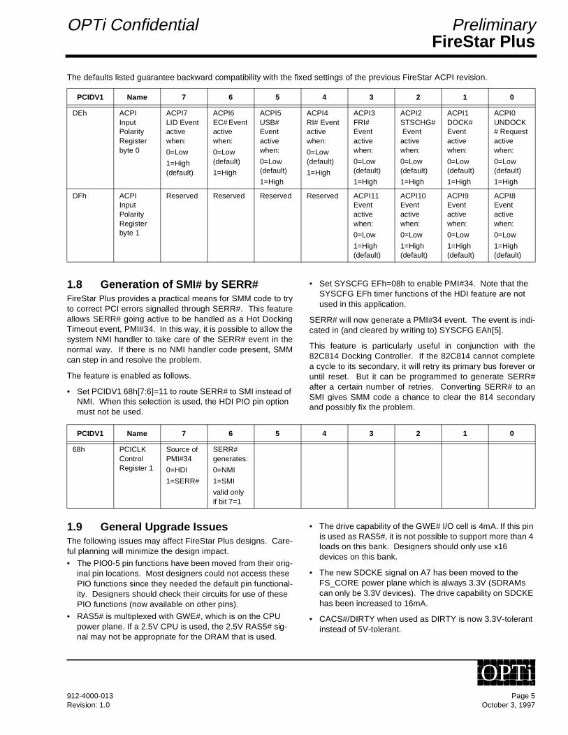
1.7 Improved ACPI FunctionalitySCI Interrupt. An SCI can now generate any interrupt fromthe group IRQ9,10,11,13. Selection bits for this function areshown below.
ACPI Input Polarity. ACPI inputs now have individuallyselectable polarity. The "active" polarity is the one thatcauses an SCI. The new registers shown below select the
polarity of each ACPI input, regardless of the source (IRQdriveback, discrete PIO pin input, multiplexed PIO pin input,or multiplexed Extended Mode input).
CPUCLK
ADS#
BRDY#
STPCLK#
DCCEN
IOW# to activate DCCEN STPGNT
End of timer
Start of timer
PCIDV1 Name 7 6 5 4 3 2 1 0
EFh ACPI Misc. Con-trol Regis-ter
Reserved Reserved Reserved Reserved Reserved Select IRQ13 as level mode
0=No
1=Yes
System IRQ used for SCI
00=IRQ9 (default)
01=IRQ10
10=IRQ11
11=IRQ13
Page 4 912-4000-013October 3, 1997 Revision: 1.0
OPTi®
FireStar PlusOPTi Confidential Preliminary
The defaults listed guarantee backward compatibility with the fixed settings of the previous FireStar ACPI revision.
1.8 Generation of SMI# by SERR#FireStar Plus provides a practical means for SMM code to tryto correct PCI errors signalled through SERR#. This featureallows SERR# going active to be handled as a Hot DockingTimeout event, PMI#34. In this way, it is possible to allow thesystem NMI handler to take care of the SERR# event in thenormal way. If there is no NMI handler code present, SMMcan step in and resolve the problem.
The feature is enabled as follows.
• Set PCIDV1 68h[7:6]=11 to route SERR# to SMI instead of NMI. When this selection is used, the HDI PIO pin option must not be used.
• Set SYSCFG EFh=08h to enable PMI#34. Note that the SYSCFG EFh timer functions of the HDI feature are not used in this application.
SERR# will now generate a PMI#34 event. The event is indi-cated in (and cleared by writing to) SYSCFG EAh[5].
This feature is particularly useful in conjunction with the82C814 Docking Controller. If the 82C814 cannot completea cycle to its secondary, it will retry its primary bus forever oruntil reset. But it can be programmed to generate SERR#after a certain number of retries. Converting SERR# to anSMI gives SMM code a chance to clear the 814 secondaryand possibly fix the problem.
1.9 General Upgrade IssuesThe following issues may affect FireStar Plus designs. Care-ful planning will minimize the design impact.
• The PIO0-5 pin functions have been moved from their orig-inal pin locations. Most designers could not access these PIO functions since they needed the default pin functional-ity. Designers should check their circuits for use of these PIO functions (now available on other pins).
• RAS5# is multiplexed with GWE#, which is on the CPU power plane. If a 2.5V CPU is used, the 2.5V RAS5# sig-nal may not be appropriate for the DRAM that is used.
• The drive capability of the GWE# I/O cell is 4mA. If this pin is used as RAS5#, it is not possible to support more than 4 loads on this bank. Designers should only use x16 devices on this bank.
• The new SDCKE signal on A7 has been moved to the FS_CORE power plane which is always 3.3V (SDRAMs can only be 3.3V devices). The drive capability on SDCKE has been increased to 16mA.
• CACS#/DIRTY when used as DIRTY is now 3.3V-tolerant instead of 5V-tolerant.
PCIDV1 Name 7 6 5 4 3 2 1 0
DEh ACPI Input Polarity Register byte 0
ACPI7 LID Event active when:
0=Low
1=High (default)
ACPI6 EC# Event active when:
0=Low (default)
1=High
ACPI5 USB# Event active when:
0=Low (default)
1=High
ACPI4 RI# Event active when:
0=Low (default)
1=High
ACPI3 FRI# Event active when:
0=Low (default)
1=High
ACPI2 STSCHG# Event active when:
0=Low (default)
1=High
ACPI1 DOCK# Event active when:
0=Low (default)
1=High
ACPI0 UNDOCK# Request active when:
0=Low (default)
1=High
DFh ACPI Input Polarity Register byte 1
Reserved Reserved Reserved Reserved ACPI11 Event active when:
0=Low
1=High (default)
ACPI10 Event active when:
0=Low
1=High (default)
ACPI9 Event active when:
0=Low
1=High (default)
ACPI8 Event active when:
0=Low
1=High (default)
PCIDV1 Name 7 6 5 4 3 2 1 0
68h PCICLK Control Register 1
Source of PMI#34
0=HDI
1=SERR#
SERR# generates:
0=NMI
1=SMI
valid only if bit 7=1
912-4000-013 Page 5Revision: 1.0 October 3, 1997
OPTi®
FireStar PlusPreliminary OPTi Confidential
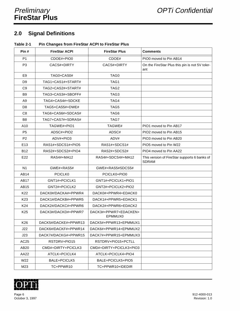
2.0 Signal Definitions
Table 2-1 Pin Changes from FireStar ACPI to FireStar Plus
Pin # FireStar ACPI FireStar Plus Comments
P1 CDOE#+PIO0 CDOE# PIO0 moved to Pin AB14
P3 CACS#+DIRTY CACS#+DIRTY On the FireStar Plus this pin is not 5V toler-ant
E9 TAG0+CAS0# TAG0
D9 TAG1+CAS1#+START# TAG1
C9 TAG2+CAS2#+START# TAG2
B9 TAG3+CAS3#+SBOFF# TAG3
A9 TAG4+CAS4#+SDCKE TAG4
D8 TAG5+CAS5#+DWE# TAG5
C8 TAG6+CAS6#+SDCAS# TAG6
B8 TAG7+CAS7#+SDRAS# TAG7
A10 TAGWE#+PIO1 TAGWE# PIO1 moved to Pin AB17
P5 ADSC#+PIO2 ADSC# PIO2 moved to Pin AB15
P2 ADV#+PIO3 ADV# PIO3 moved to Pin AB20
E13 RAS1#+SDCS1#+PIO5 RAS1#+SDCS1# PIO5 moved to Pin W22
B12 RAS2#+SDCS2#+PIO4 RAS2#+SDCS2# PIO4 moved to Pin AA22
E22 RAS4#+MA12 RAS4#+SDCS4#+MA12 This version of FireStar supports 6 banks of SDRAM
N1 GWE#+RAS5# GWE#+RAS5#SDCS5#
AB14 PCICLK0 PCICLK0+PIO0
AB17 GNT1#+PCICLK1 GNT1#+PCICLK1+PIO1
AB15 GNT2#+PCICLK2 GNT2#+PCICLK2+PIO2
K22 DACK0#/DACKA#+PPWR4 DACK0#+PPWR4+EDACK0
K23 DACK1#/DACKB#+PPWR5 DACK1#+PPWR5+EDACK1
K24 DACK2#/DACKC#+PPWR6 DACK2#+PPWR6+EDACK2
K25 DACK3#/DACKD#+PPWR7 DACK3#+PPWR7+EDACKEN+ EPMMUX0
K26 DACK5#/DACKE#+PPWR13 DACK5#+PPWR13+EPMMUX1
J22 DACK6#/DACKF#+PPWR14 DACK6#+PPWR14+EPMMUX2
J23 DACK7#/DACKG#+PPWR15 DACK7#+PPWR15+EPMMUX3
AC25 RSTDRV+PIO15 RSTDRV+PIO15+PCTLL
AB20 CMD#+DIRTY+PCICLK3 CMD#+DIRTY+PCICLK3+PIO3
AA22 ATCLK+PCICLK4 ATCLK+PCICLK4+PIO4
W22 BALE+PCICLK5 BALE+PCICLK5+PIO5
M23 TC+PPWR10 TC+PPWR10+IDEDIR
Page 6 912-4000-013October 3, 1997 Revision: 1.0
OPTi®
FireStar PlusOPTi Confidential Preliminary
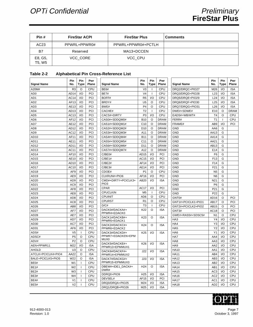
Table 2-2 Alphabetical Pin Cross-Reference List
AC23 PPWRL+PPWR0# PPWRL+PPWR0#+PCTLH
B7 Reserved MA13+DCCEN
E8, G5,T5, W5
VCC_CORE VCC_CPU
Pin # FireStar ACPI FireStar Plus Comments
Pin Pin Pwr Pin Pin Pwr Pin Pin Pwr
Signal Name No. Type PlaneA20M# R3 O CPU
AD0 AD14 I/O PCI
AD1 AC14 I/O PCI
AD2 AF13 I/O PCI
AD3 AE13 I/O PCI
AD4 AD13 I/O PCI
AD5 AC13 I/O PCI
AD6 AF12 I/O PCI
AD7 AE12 I/O PCI
AD8 AD12 I/O PCI
AD9 AC12 I/O PCI
AD10 AF11 I/O PCI
AD11 AE11 I/O PCI
AD12 AD11 I/O PCI
AD13 AC11 I/O PCI
AD14 AF10 I/O PCI
AD15 AE10 I/O PCI
AD16 AD10 I/O PCI
AD17 AC10 I/O PCI
AD18 AF9 I/O PCI
AD19 AE9 I/O PCI
AD20 AD9 I/O PCI
AD21 AC9 I/O PCI
AD22 AF8 I/O PCI
AD23 AE8 I/O PCI
AD24 AD8 I/O PCI
AD25 AC8 I/O PCI
AD26 AB8 I/O PCI
AD27 AF7 I/O PCI
AD28 AE7 I/O PCI
AD29 AD7 I/O PCI
AD30 AC7 I/O PCI
AD31 AF6 I/O PCI
ADS# V5 I CPU
ADSC# P5 O CPU
ADV# P2 O CPU
AEN+PPWR11 M22 I/O ISA
AHOLD U3 O CPU
ATCLK+PCICLK4+PIO4 AA22 O ISA
BALE+PCICLK5+PIO5 W22 O ISA
BE0# W1 I CPU
BE1# W2 I CPU
BE2# W3 I CPU
BE3# W4 I CPU
BE4# V1 I CPU
BE5# V2 I CPU
BE6# V3 I CPU
BE7# V4 I CPU
BOFF# R5 I/O CPU
BRDY# U5 O CPU
BWE# P4 O CPU
CACHE# T2 I CPU
CACS#+DIRTY P3 I/O CPU
CAS0#+SDDQM0# B10 O DRAM
CAS1#+SDDQM1# C10 O DRAM
CAS2#+SDDQM2# D10 O DRAM
CAS3#+SDDQM3# A11 O DRAM
CAS4#+SDDQM4# B11 O DRAM
CAS5#+SDDQM5# C11 O DRAM
CAS6#+SDDQM6# D11 O DRAM
CAS7#+SDDQM7# A12 O DRAM
C/BE0# AD15 I/O PCI
C/BE1# AC15 I/O PCI
C/BE2# AF14 I/O PCI
C/BE3# AE14 I/O PCI
CDOE# P1 O CPU
CLKRUN#+PIO6 AF16 I/O PCI
CMD#+DIRTY+PCICLK3+PIO3
AB20 I/O ISA
CPAR AC17 I/O PCI
CPUCLKIN M5 I CPU
CPUINIT AD6 O CPU
CPURST R1 O CPU
D/C# T3 I CPU
DACK0#/DACKA#+PPWR4+EDACK0
K22 O ISA
DACK1#/DACKB#+PPWR5+EDACK1
K23 O ISA
DACK2#/DACKC#+PPWR6+EDACK2
K24 O ISA
DACK3#/DACKD#+PPWR7+EDACKEN+EPMMUX0
K25 I/O ISA
DACK5#/DACKE#+PPWR13+EPMMUX1
K26 I/O ISA
DACK6#/DACKF#+PPWR14+EPMMUX2
J22 I/O ISA
DACK7#/DACKG#+PPWR15+EPMMUX3
J23 I/O ISA
DBEW#+IDE1_DACK#+DWR#
H24 O ISA
DDRQ0+PIO9 H25 I/O ISA
DEVSEL# AF15 I/O PCI
DRQ0/DRQA+PIO25 M24 I/O ISA
DRQ1/DRQB+PIO26 M25 I/O ISA
Signal Name No. Type Plane
DRQ2/DRQC+PIO27 M26 I/O ISA
DRQ3/DRQD+PIO28 L23 I/O ISA
DRQ5/DRQE+PIO29 L24 I/O ISA
DRQ6/DRQF+PIO30 L25 I/O ISA
DRQ7/DRQG+PIO31 L26 I/O ISA
DWE#+SDWE# E10 O DRAM
EADS#+WB/WT# T4 O CPU
FERR# T1 I CPU
FRAME# AB9 I/O PCI
GND AA6 G
GND AA13 G
GND AA14 G
GND AA21 G
GND AB13 G
GND E14 G
GND F6 G
GND F13 G
GND F14 G
GND F21 G
GND N5 G
GND N6 G
GND N21 G
GND P6 G
GND P21 G
GND P22 G
GNT0# AD16 O PCI
GNT1#+PCICLK1+PIO1 AB17 O PCI
GNT2#+PCICLK2+PIO2 AB15 O PCI
GNT3# AC18 O PCI
GWE#+RAS5#+SDSC5# N1 O CPU
HA3 Y4 I/O CPU
HA4 Y3 I/O CPU
HA5 Y2 I/O CPU
HA6 Y1 I/O CPU
HA7 AA4 I/O CPU
HA8 AA3 I/O CPU
HA9 AA2 I/O CPU
HA10 AA1 I/O CPU
HA11 AB4 I/O CPU
HA12 AB3 I/O CPU
HA13 AB2 I/O CPU
HA14 AB1 I/O CPU
HA15 AC3 I/O CPU
HA16 AC2 I/O CPU
HA17 AC1 I/O CPU
HA18 AD2 I/O CPU
Signal Name No. Type Plane
912-4000-013 Page 7Revision: 1.0 October 3, 1997
OPTi®
FireStar PlusPreliminary OPTi Confidential
HA19 AD1 I/O CPU
HA20 AE1 I/O CPU
HA21 AF1 I/O CPU
HA22 AE2 I/O CPU
HA23 AF2 I/O CPU
HA24 AD3 I/O CPU
HA25 AE3 I/O CPU
HA26 AF3 I/O CPU
HA27 AC4 I/O CPU
HA28 AD4 I/O CPU
HA29 AE4 I/O CPU
HA30 AF4 I/O CPU
HA31 AC5 I/O CPU
HD0 N2 I/O CPU
HD1 N3 I/O CPU
HD2 N4 I/O CPU
HD3 M1 I/O CPU
HD4 M2 I/O CPU
HD5 M3 I/O CPU
HD6 M4 I/O CPU
HD7 L1 I/O CPU
HD8 L2 I/O CPU
HD9 L3 I/O CPU
HD10 L4 I/O CPU
HD11 L5 I/O CPU
HD12 K1 I/O CPU
HD13 K2 I/O CPU
HD14 K3 I/O CPU
HD15 K4 I/O CPU
HD16 J1 I/O CPU
HD17 J2 I/O CPU
HD18 J3 I/O CPU
HD19 J4 I/O CPU
HD20 J5 I/O CPU
HD21 H1 I/O CPU
HD22 H2 I/O CPU
HD23 H3 I/O CPU
HD24 H4 I/O CPU
HD25 H5 I/O CPU
HD26 G1 I/O CPU
HD27 G2 I/O CPU
HD28 G3 I/O CPU
HD29 G4 I/O CPU
HD30 F1 I/O CPU
HD31 F2 I/O CPU
HD32 F3 I/O CPU
HD33 F4 I/O CPU
HD34 F5 I/O CPU
HD35 E1 I/O CPU
HD36 E2 I/O CPU
HD37 E3 I/O CPU
HD38 E4 I/O CPU
HD39 D1 I/O CPU
HD40 D2 I/O CPU
HD41 D3 I/O CPU
HD42 D4 I/O CPU
HD43 C1 I/O CPU
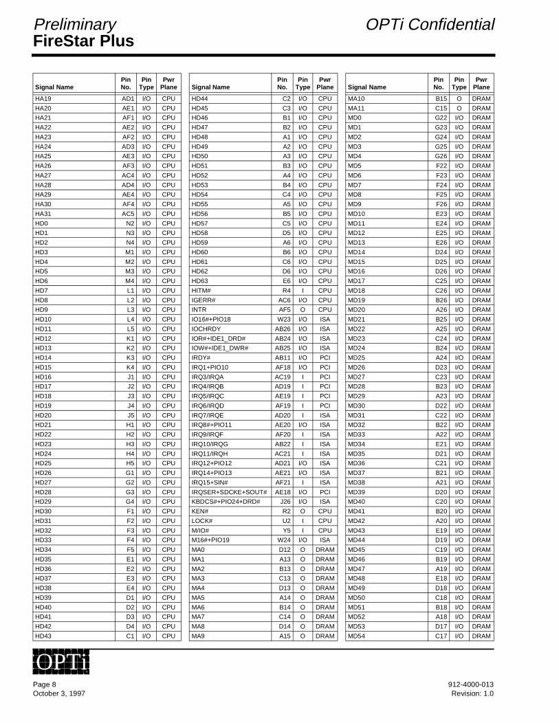
Signal NamePin No.
Pin Type
Pwr Plane
HD44 C2 I/O CPU
HD45 C3 I/O CPU
HD46 B1 I/O CPU
HD47 B2 I/O CPU
HD48 A1 I/O CPU
HD49 A2 I/O CPU
HD50 A3 I/O CPU
HD51 B3 I/O CPU
HD52 A4 I/O CPU
HD53 B4 I/O CPU
HD54 C4 I/O CPU
HD55 A5 I/O CPU
HD56 B5 I/O CPU
HD57 C5 I/O CPU
HD58 D5 I/O CPU
HD59 A6 I/O CPU
HD60 B6 I/O CPU
HD61 C6 I/O CPU
HD62 D6 I/O CPU
HD63 E6 I/O CPU
HITM# R4 I CPU
IGERR# AC6 I/O CPU
INTR AF5 O CPU
IO16#+PIO18 W23 I/O ISA
IOCHRDY AB26 I/O ISA
IOR#+IDE1_DRD# AB24 I/O ISA
IOW#+IDE1_DWR# AB25 I/O ISA
IRDY# AB11 I/O PCI
IRQ1+PIO10 AF18 I/O PCI
IRQ3/IRQA AC19 I PCI
IRQ4/IRQB AD19 I PCI
IRQ5/IRQC AE19 I PCI
IRQ6/IRQD AF19 I PCI
IRQ7/IRQE AD20 I ISA
IRQ8#+PIO11 AE20 I/O ISA
IRQ9/IRQF AF20 I ISA
IRQ10/IRQG AB22 I ISA
IRQ11/IRQH AC21 I ISA
IRQ12+PIO12 AD21 I/O ISA
IRQ14+PIO13 AE21 I/O ISA
IRQ15+SIN# AF21 I ISA
IRQSER+SDCKE+SOUT# AE18 I/O PCI
KBDCS#+PIO24+DRD# J26 I/O ISA
KEN# R2 O CPU
LOCK# U2 I CPU
M/IO# Y5 I CPU
M16#+PIO19 W24 I/O ISA
MA0 D12 O DRAM
MA1 A13 O DRAM
MA2 B13 O DRAM
MA3 C13 O DRAM
MA4 D13 O DRAM
MA5 A14 O DRAM
MA6 B14 O DRAM
MA7 C14 O DRAM
MA8 D14 O DRAM
MA9 A15 O DRAM
Signal NamePin No.
Pin Type
Pwr Plane
MA10 B15 O DRAM
MA11 C15 O DRAM
MD0 G22 I/O DRAM
MD1 G23 I/O DRAM
MD2 G24 I/O DRAM
MD3 G25 I/O DRAM
MD4 G26 I/O DRAM
MD5 F22 I/O DRAM
MD6 F23 I/O DRAM
MD7 F24 I/O DRAM
MD8 F25 I/O DRAM
MD9 F26 I/O DRAM
MD10 E23 I/O DRAM
MD11 E24 I/O DRAM
MD12 E25 I/O DRAM
MD13 E26 I/O DRAM
MD14 D24 I/O DRAM
MD15 D25 I/O DRAM
MD16 D26 I/O DRAM
MD17 C25 I/O DRAM
MD18 C26 I/O DRAM
MD19 B26 I/O DRAM
MD20 A26 I/O DRAM
MD21 B25 I/O DRAM
MD22 A25 I/O DRAM
MD23 C24 I/O DRAM
MD24 B24 I/O DRAM
MD25 A24 I/O DRAM
MD26 D23 I/O DRAM
MD27 C23 I/O DRAM
MD28 B23 I/O DRAM
MD29 A23 I/O DRAM
MD30 D22 I/O DRAM
MD31 C22 I/O DRAM
MD32 B22 I/O DRAM
MD33 A22 I/O DRAM
MD34 E21 I/O DRAM
MD35 D21 I/O DRAM
MD36 C21 I/O DRAM
MD37 B21 I/O DRAM
MD38 A21 I/O DRAM
MD39 D20 I/O DRAM
MD40 C20 I/O DRAM
MD41 B20 I/O DRAM
MD42 A20 I/O DRAM
MD43 E19 I/O DRAM
MD44 D19 I/O DRAM
MD45 C19 I/O DRAM
MD46 B19 I/O DRAM
MD47 A19 I/O DRAM
MD48 E18 I/O DRAM
MD49 D18 I/O DRAM
MD50 C18 I/O DRAM
MD51 B18 I/O DRAM
MD52 A18 I/O DRAM
MD53 D17 I/O DRAM
MD54 C17 I/O DRAM
Signal NamePin No.
Pin Type
Pwr Plane
Page 8 912-4000-013October 3, 1997 Revision: 1.0
OPTi®

FireStar PlusOPTi Confidential Preliminary
Power Plane Key:CORE = 3.3V OnlyCPU = 3.3V/2.5VDRAM = 3.3V or 5.0VISA = 3.3V or 5.0VPCI = 3.3V or 5.0V
Note: The pins listed below are 5.0V tolerant inputs, even when their power plane is connected to 3.3V as long as the 5VREF pins of FireStar are connected to +5.0V:
OSC32OSC_14MHZPCICLKIRQAIRQBIRQCIRQDIRQ1
MD55 B17 I/O DRAM
MD56 A17 I/O DRAM
MD57 E16 I/O DRAM
MD58 D16 I/O DRAM
MD59 C16 I/O DRAM
MD60 B16 I/O DRAM
MD61 A16 I/O DRAM
MD62 E15 I/O DRAM
MD63 D15 I/O DRAM
MRD#+IDE1_DCS3# AC26 I/O ISA
MWR#+IDE1_DCS1# AB23 I/O ISA
NA# U4 O CPU
NMI AD5 O CPU
OSC_14MHZ E5 I CORE
OSC32 C7 I CORE
PCICLK0+PIO0 AB14 I/O PCI
PCICLKIN AB6 I CORE
PERR# AE17 I/O PCI
PLOCK# AE15 I/O PCI
PPWRL+PPWR0#+PCTLH AC23 O ISA
PWRGD H26 I ISA
RAS0#+SDCS0# E12 O DRAM
RAS1#+SDCS1# E13 O DRAM
RAS2#+SDCS2# B12 O DRAM
RAS3#+SDCS3#+MA12 C12 O DRAM
RAS4#+SDCS4#+MA12 E22 O DRAM
RFSH#+PPWR12 J25 I/O ISA
REQ0# AF17 I PCI
REQ1#+PIO7 AB18 I/O PCI
REQ2#+PIO8 AE16 I/O PCI
REQ3# AD18 I PCI
RESET# AC24 O ISA
ROMCS#+PIO23+ROMCS#/KBDCS#
J24 I/O ISA
RSTDRV+PIO15+PCTLL AC25 I/O ISA
RTCAS+IDE1_DA0 N24 I/O ISA
RTCRD#+IDE1_DA1 N25 I/O ISA
RTCWR#+IDE1_DA2 N26 I/O ISA
SA0+IDE1_DD0 N23 I/O ISA
SA1+IDE1_DD1 N22 I/O ISA
SA2+IDE1_DD2 P26 I/O ISA
SA3+IDE1_DD3 P25 I/O ISA
SA4+IDE1_DD4 P24 I/O ISA
SA5+IDE1_DD5 P23 I/O ISA
SA6+IDE1_DD6 R26 I/O ISA
SA7+IDE1_DD7 R25 I/O ISA
SA8+IDE1_DD8 R24 I/O ISA
SA9+IDE1_DD9 R23 I/O ISA
SA10+IDE1_DD10 R22 I/O ISA
SA11+IDE1_DD11 T26 I/O ISA
SA12+IDE1_DD12 T25 I/O ISA
SA13+IDE1_DD13 T24 I/O ISA
SA14+IDE1_DD14 T23 I/O ISA
SA15+IDE1_DD15 T22 I/O ISA
SA16+PIO16 U26 I/O ISA
SA17+PIO17 U25 I/O ISA
SA18+PPWR8 U24 I/O ISA
Signal NamePin No.
Pin Type
Pwr Plane
SA19+PPWR9 U23 I/O ISA
SA20+PPWR0 V26 I/O ISA
SA21+PPWR1 V25 I/O ISA
SA22+PPWR2 V24 I/O ISA
SA23+PPWR3 V23 I/O ISA
SBHE#+PIO20 W25 I/O ISA
SD0+MAD0 AD26 I/O ISA
SD1+MAD1 AD25 I/O ISA
SD2+MAD2 AD24 I/O ISA
SD3+MAD3 AE26 I/O ISA
SD4+MAD4 AE25 I/O ISA
SD5+MAD5 AF26 I/O ISA
SD6+MAD6 AF25 I/O ISA
SD7+MAD7 AF24 I/O ISA
SD8+MAD8 AE24 I/O ISA
SD9+MAD9 AF23 I/O ISA
SD10+MAD10 AE23 I/O ISA
SD11+MAD11 AD23 I/O ISA
SD12+MAD12 AF22 I/O ISA
SD13+MAD13 AE22 I/O ISA
SD14+MAD14 AD22 I/O ISA
SD15+MAD15 AC22 I/O ISA
SDCAS# A8 O DRAM
SDRAS# D7 O DRAM
SEL#/ATB#+SDCKE+PIO14
AC20 I/O ISA
SERR# AD17 I/O PCI
SMI# AE5 O CPU
SMIACT# U1 I CPU
SMRD#+PIO21 W26 I/O ISA
SMWR#+PIO22 V22 I/O ISA
SPKOUT H23 I/O ISA
STOP# AC16 I/O PCI
STPCLK# AE6 O CPU
TAG0 E9 I/O DRAM
TAG1 D9 I/O DRAM
TAG2 C9 I/O DRAM
TAG3 B9 I/O DRAM
TAG4 A9 I/O DRAM
TAG5 D8 I/O DRAM
TAG6 C8 I/O DRAM
TAG7 B8 I/O DRAM
TAGWE# A10 O DRAM
TC+PPWR10+IDEDIR M23 I/O ISA
MA13+DCC B7 I/O DRAM
SDCKE A7 I/O DRAM
TMS AB5 I/O CPU
TRDY# AB12 I/O PCI
VCC_CORE H22 P
VCC_CORE K5 P
VCC_CORE AB19 P
VCC_CPU E8 P
VCC_CPU G5 P
VCC_CPU T5 P
VCC_CPU W5 P
VCC_DRAM E11 P
VCC_DRAM E17 P
Signal NamePin No.
Pin Type
Pwr Plane
VCC_DRAM E20 P
VCC_ISA L22 P
VCC_ISA U22 P
VCC_ISA Y22 P
VCC_PCI AB7 P
VCC_PCI AB10 P
VCC_PCI AB16 P
W/R#+INV AA5 I/O CPU
XD0+IDE_DWR# Y26 I/O ISA
XD1+IDE_DRD# Y25 I/O ISA
XD2+IDE_DA0 Y24 I/O ISA
XD3+IDE_DA1 Y23 I/O ISA
XD4+IDE_DA2 AA26 I/O ISA
XD5+IDE_DDACK# AA25 I/O ISA
XD6+IDE_DCS1# AA24 I/O ISA
XD7+IDE_DCS3# AA23 I/O ISA
5VREF AB21 P
5VREF E7 P
Signal NamePin No.
Pin Type
Pwr Plane
912-4000-013 Page 9Revision: 1.0 October 3, 1997
OPTi®
FireStar PlusPreliminary OPTi Confidential
3.0 Clock Signal Specifications
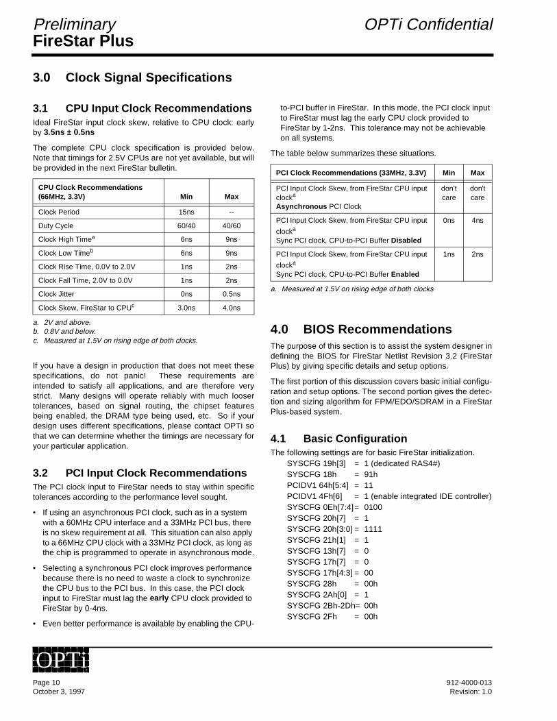
3.1 CPU Input Clock RecommendationsIdeal FireStar input clock skew, relative to CPU clock: earlyby 3.5ns ± 0.5ns
The complete CPU clock specification is provided below.Note that timings for 2.5V CPUs are not yet available, but willbe provided in the next FireStar bulletin.
If you have a design in production that does not meet thesespecifications, do not panic! These requirements areintended to satisfy all applications, and are therefore verystrict. Many designs will operate reliably with much loosertolerances, based on signal routing, the chipset featuresbeing enabled, the DRAM type being used, etc. So if yourdesign uses different specifications, please contact OPTi sothat we can determine whether the timings are necessary foryour particular application.
3.2 PCI Input Clock RecommendationsThe PCI clock input to FireStar needs to stay within specifictolerances according to the performance level sought.
• If using an asynchronous PCI clock, such as in a system with a 60MHz CPU interface and a 33MHz PCI bus, there is no skew requirement at all. This situation can also apply to a 66MHz CPU clock with a 33MHz PCI clock, as long as the chip is programmed to operate in asynchronous mode.
• Selecting a synchronous PCI clock improves performance because there is no need to waste a clock to synchronize the CPU bus to the PCI bus. In this case, the PCI clock input to FireStar must lag the early CPU clock provided to FireStar by 0-4ns.
• Even better performance is available by enabling the CPU-
a. 2V and above.b. 0.8V and below.c. Measured at 1.5V on rising edge of both clocks.
to-PCI buffer in FireStar. In this mode, the PCI clock input to FireStar must lag the early CPU clock provided to FireStar by 1-2ns. This tolerance may not be achievable on all systems.
The table below summarizes these situations.
4.0 BIOS RecommendationsThe purpose of this section is to assist the system designer indefining the BIOS for FireStar Netlist Revision 3.2 (FireStarPlus) by giving specific details and setup options.
The first portion of this discussion covers basic initial configu-ration and setup options. The second portion gives the detec-tion and sizing algorithm for FPM/EDO/SDRAM in a FireStarPlus-based system.
4.1 Basic ConfigurationThe following settings are for basic FireStar initialization.
SYSCFG 19h[3] = 1 (dedicated RAS4#)SYSCFG 18h = 91hPCIDV1 64h[5:4] = 11PCIDV1 4Fh[6] = 1 (enable integrated IDE controller)SYSCFG 0Eh[7:4]= 0100SYSCFG 20h[7] = 1SYSCFG 20h[3:0] = 1111SYSCFG 21h[1] = 1SYSCFG 13h[7] = 0SYSCFG 17h[7] = 0SYSCFG 17h[4:3] = 00SYSCFG 28h = 00hSYSCFG 2Ah[0] = 1SYSCFG 2Bh-2Dh= 00hSYSCFG 2Fh = 00h
a. Measured at 1.5V on rising edge of both clocks
CPU Clock Recommendations(66MHz, 3.3V) Min Max
Clock Period 15ns --
Duty Cycle 60/40 40/60
Clock High Timea 6ns 9ns
Clock Low Timeb 6ns 9ns
Clock Rise Time, 0.0V to 2.0V 1ns 2ns
Clock Fall Time, 2.0V to 0.0V 1ns 2ns
Clock Jitter 0ns 0.5ns
Clock Skew, FireStar to CPUc 3.0ns 4.0ns
PCI Clock Recommendations (33MHz, 3.3V) Min Max
PCI Input Clock Skew, from FireStar CPU input clocka
Asynchronous PCI Clock
don't care
don't care
PCI Input Clock Skew, from FireStar CPU input
clocka
Sync PCI clock, CPU-to-PCI Buffer Disabled
0ns 4ns
PCI Input Clock Skew, from FireStar CPU input
clocka
Sync PCI clock, CPU-to-PCI Buffer Enabled
1ns 2ns
Page 10 912-4000-013October 3, 1997 Revision: 1.0
OPTi®
FireStar PlusOPTi Confidential Preliminary
SYSCFG 22h[7] = 0SYSCFG 11h[3] = 1 (if L2 is to be enabled)SYSCFG 1Fh[1] = 1PCIDV1 71h[0] = 1SYSCFG 1Eh = CChSYSCFG 1Dh[5] = 1SYSCFG 08h[6] = 0SYSCFG 08h[1] = 11
SYSCFG 16h[7] = 1 (sets the CMD# pin as CMD#)SYSCFG 23h[2:1] = 11PCIDV0 42h[1] = 1SYSCFG 11h[1:0] = 11SYSCFG 15h[7:4] = 1010SYSCFG 15h[0] = 0SYSCFG 00h[6] = 1SYSCFG 10h[5] = 1SYSCFG 0Fh[5] = 0 (set to 1 only when L2 is in WT
mode and CPU-to-DRAM buffer isenabled)
Note: 1. The BIOS must write the subsystem vendor ID inPCIDV0 2Ch-2Fh, PCIDV1 2Ch-2Fh, and PCI-IDE 2Ch-2Fh.
These registers are one time writable and mustbe written by the BIOS before giving control tothe OS. These registers may be initialized to 0 ifa subsystem vendor ID value is not available.
4.2 Preliminary Memory ConfigurationSYSCFG 14h[7] must be enabled prior to setting PCIDV044h[0]. These two bits can be set prior to performing FPM/EDO autodetection.
SYSCFG 14h[7] = 1 (enable prior to setting PCIDV044h[0])
PCIDV0 44h[0] = 1
Note: The restriction of 32-bit write operations to PCIDV0 44h has been removed.
4.3 Setup OptionsThe BIOS must follow the specific enable or disablesequence for setup options marked with an asterisk (*). How-ever, if the BIOS can guarantee no DRAM accesses in thecourse of enabling or disabling these options, the order is notimportant.
1. SYSCFG 08h[1] should be set to 1 prior to loading any op-tion ROMs, i.e prior to the BIOS performing the PCI Busscan.
4.3.1 Refresh ModeA. ISA Refresh:
SYSCFG 2Eh[6] = 1PCIDV1 64h[0] = 0SYSCFG 27h[2:0] = 000PCIDV1 47h[6] = 0
B. Hidden Refresh:SYSCFG 2Eh[6] = 1PCIDV1 64h[0] = 0SYSCFG 27h[2:0] = 000PCIDV1 47h[6] = 1
C. Non-ISA Refresh: (recommended default)PCIDV1 64h[0] = 1SYSCFG 27h[2:0] = 100 for 66MHz CPUCLK
= 101 for 60MHz CPUCLK= 110 for 50MHz CPUCLK= 111 for 40MHz CPUCLK
SYSCFG 2Eh[6] = 0PCIDV1 47h[6] = 0
D. Burst Refresh (same as non-ISA refresh with inclusion of SYSCFG 2Fh[2:0]) :PCIDV1 64h[0] = 1SYSCFG 27h[2:0] = 100 for 66MHz CPUCLK
= 101 for 60MHz CPUCLK= 110 for 50MHz CPUCLK= 111 for 40MHz CPUCLK
SYSCFG 2Eh[6] = 0PCIDV1 47h[6] = 0SYSCFG 2Fh[2:0] = 001
E. Enable SDRAM Self-Refresh in Suspend:SYSCFG 12h[5:4] = 01SYSCFG 2Eh[7] = 1SYSCFG 61h[2] = 1SYSCFG 66h[7,0] = 1,1SYSCFG 68h[0] = 1SYSCFG 6Bh[7] = 1
Note: Refer to Figure 4-1 for information regarding switch-ing between refresh modes.
4.3.2 PCICLKA. Asynchronous (default):
SYSCFG 10h[0] = 0SYSCFG 16h[2] = 0
B. Synchronous :SYSCFG 10h[0] = 1SYSCFG 16h[2] = 1
4.3.3 PCI Post WriteA. Disable:
912-4000-013 Page 11Revision: 1.0 October 3, 1997
OPTi®
FireStar PlusPreliminary OPTi Confidential
SYSCFG 15h[5:4] = 00
B. Post/No Burst:SYSCFG 15h[5:4] = 01
C. Post/Burst (default):SYSCFG 15h[5:4] = 10
D. Post/Fast BurstSYSCFG 15h[5:4] = 11
4.3.4 ISA RetryA. Disable (default):
PCIDV1 65h[1] = 0PCIDV0 4Ch[3] = 0PCIDV0 4Fh[1] = 0PCIDV0 47h[7] = 0PCIDV0 47h[5] = 0PCIDV0 47h[2] = 0PCIDV0 4Fh[7:2] = 000000PCIDV0 57h[7:2] = 000000SYSCFG 22h[4] = 0SYSCFG 1Eh[4] = 0SYSCFG 1Eh[3] = 1SYSCFG 18h[7] = 0
B. Enable1:SYSCFG 18h[7] = 1SYSCFG 1Eh[4:3]= 11SYSCFG 22h[4] = 1PCIDV0 57h[7:2] = 111111PCIDV0 4Fh[7:2] = 000000PCIDV0 47h[2] = 1PCIDV0 47h[5] = 02
PCIDV0 47h[7] = 1PCIDV0 4Fh[1] = 0PCIDV0 4Ch[3] = 1PCIDV1 65h[1] = 1
4.3.5 Buffered DMA 3
A Disable (default):SYSCFG 0Eh[6] = 1SYSCFG 1Dh[3] = 0PCIDV1 43h[7:6] = 00
B. Enable4:Enable ISA retry
1. Prior to enabling the ISA retry feature the C2D Buffer has tobe enabled.
2. Note that the current P2D FIFO code for Rev 2.2 setsPCIDV0 47h[5] = 1. For the 3.2 silicon when ISA retry/BDMAis enabled the P2D FIFO should not set PCIDV0 47h[5] = 1.
3. Buffered DMA has to be enabled once ISA retry has beenenabled.
SYSCFG 0Eh[6] = 0SYSCFG 1Dh[3] = 1PCIDV1 43h[7:6] = 11PCIDV1 67h[5] = 1
4.3.6 L2 Cache ControlA. L2 Cache Enable5:
SYSCFG 08h[7] = 1SYSCFG 08h[3] = 1SYSCFG 16h[7] = 1SYSCFG 16h[5] = 1SYSCFG 11h[3] = 16
PCIDV0 4Ch[6] = 1
4.3.7 Cache 3-1-1-1-1-1-1-1 control A. Disable (default):
SYSCFG 04h[3] = 0SYSCFG 10h[5] = 0
B. Enable:SYSCFG 10h[5] = 1SYSCFG 04h[3] = 1
4.3.8 CAS PrechargeA. 2 CLKS:
SYSCFG 02h[0] = 0
B. 1 CLK: (recommended default)SYSCFG 02h[0] = 1
4.3.9 DRAM PipeliningA. Disabled (default):
SYSCFG 08h[2] = 0SYSCFG 11h[4] = 0SYSCFG 1Fh[5] = 0
B. Slow (X222-X222)SYSCFG 08h[2] = 0SYSCFG 11h[4] = 1SYSCFG 1Fh[5] = 0
C. Fast (X222-3222)SYSCFG 1Fh[5] = 1SYSCFG 08h[2] = 1SYSCFG 11h[4] = 0
D. Aggressive (X222-2222)
4. DRAM byte merge should be enabled for reliable BufferedDMA operation
5. On the 2.2 Rev, these bits were hardcoded in the silicon andhence the BIOS did not need to program these bits. On the3.2 silicon, these bits need to be programmed to enable theL2 cache
6. Note that the current code for the 2.2 silicon may be settingSYSCFG 11h[3] = 0. One needs to make sure that this bit isset to 1.
Page 12 912-4000-013October 3, 1997 Revision: 1.0
OPTi®
FireStar PlusOPTi Confidential Preliminary
SYSCFG 1Fh[5] = 0SYSCFG 08h[2] = 1SYSCFG 11h[4] = 0
4.3.10 DRAM Post WriteA. Disable:
SYSCFG 02h[1] = 0 SYSCFG 0Ch[6] = 0
B. Enable:SYSCFG 02h[1] = 1SYSCFG 0Ch[6] = 0
C. Fast: (recommended default)SYSCFG 02h[1] = 1SYSCFG 0Ch[6] = 1
4.3.11 *CPU Write to DRAM BufferA. Disable (default):
PCIDV0 44h[4] = 0SYSCFG 2Ch[0] = 0
B. Enable (must be enabled if SDRAM is detected) (recom-mend that this is enabled always):SYSCFG 01h[2] = 1SYSCFG 02h[0] = 1SYSCFG 02h[1] = 1 (DRAM post write option will also
set this bit)SYSCFG 2Ch[0] = 1PCIDV0 44h[4] = 1
4.3.12 SDRAM CAS#/Burst OrderA. 3/Intel (default):
SYSCFG 28h = 3Ah
B. 3/CyrixSYSCFG 28h = 32h
C. 2/IntelSYSCFG 28h = 2Ah
D. 2/CyrixSYSCFG 28h = 22h
4.3.13 *DRAM Byte MergeA. Disable (default):
SYSCFG 2Ch[1] = 0PCIDV0 45h[1] = 0
B. Enable:SYSCFG 2Ch[1] = 1PCIDV0 45h[1] = 1
4.3.14 *DRAM Read-AroundA. Disable (default):
SYSCFG 2Ch[5] = 0
PCIDV0 45h[5:4] = 00
B. Enable:PCIDV0 45h[5:4] = 11SYSCFG 2Ch[5] = 1
4.3.15 PCI Master Wait StatesRecommended default is X-1-1-1-1.
To achieve X-1-1-1-1 PCI master bursts for reads and writes,SYSCFG 20h[3:0] must be set to 1111 (can be hardcoded forthe default setting of X-1-1-1-1). The PCI-to-DRAM bufferMUST be enabled (default setup option). If the PCI-to-DRAMbuffer is disabled, SYSCFG 20h[3:2] can be set to either 01or 10 for X-3-3-3 or X-2-2-2 write bursts respectively, andSYSCFG 20h[1:0] can be set to either 01 or 10 for X-3-3-3 orX-2-2-2 read bursts respectively. SYSCFG 20h[3:2] orSYSCFG 20h[1:0] MUST NOT be set to 11 when the PCI-to-DRAM buffer is disabled.
4.3.16 *PCI Write to DRAM BufferA. Disable Read / Disable Write:
SYSCFG 2Ah[2] = 0PCIDV0 44h[6] = 0SYSCFG 2Ah[3] = 0PCIDV0 44h[5] = 0PCIDV1 64h[7] = 0PCIDV1 64h[6] = 0
B. Disable Read / Enable Write:SYSCFG 2Ah[2] = 0PCIDV0 44h[6] = 0PCIDV0 44h[5] = 1SYSCFG 2Ah[3] = 1PCIDV1 64h[7] = 1PCIDV1 64h[6] = 0
C. Enable Read / Disable Write:SYSCFG 2Ah[3] = 0PCIDV0 44h[5] = 0PCIDV0 44h[6] = 1SYSCFG 2Ah[2] = 1PCIDV1 64h[7] = 0PCIDV1 64h[6] = 1
D. Enable Read / Enable Write (default):PCIDV0 44h[6] = 1PCIDV0 44h[5] = 1SYSCFG 2Ah[3] = 1SYSCFG 2Ah[2] = 1PCIDV1 64h[7] = 1PCIDV1 64h[6] = 1
912-4000-013 Page 13Revision: 1.0 October 3, 1997
OPTi®
FireStar PlusPreliminary OPTi Confidential
4.3.17 *EDO Timing:First turn on EDO options in SYSCFG 1Ch[7:0].
A. 8-2-2-2 (default):SYSCFG 2Dh[5:0]= 000000SYSCFG 2Dh[6] = 0SYSCFG 26h[3] = 0SYSCFG 1Fh[4] = 0SYSCFG 1Dh[4] = 0
7-2-2-2:SYSCFG 2Dh[5:0]= 000000SYSCFG 2Dh[6] = 0SYSCFG 26h[3] = 0SYSCFG 1Dh[4] = 1 SYSCFG 1Fh[4] = 0
6-2-2-2:SYSCFG 2Dh[5:0]= 000000SYSCFG 2Dh[6] = 0SYSCFG 26h[3] = 0SYSCFG 1Dh[4] = 1SYSCFG 1Fh[4] = 1
5-2-2-2:SYSCFG 1Dh[4] = 1SYSCFG 1Fh[4] = 1SYSCFG 26h[3] = 1SYSCFG 2Dh[6] = 1SYSCFG 2Dh[5:0]= Set according to the banks that
have been detected with EDO
Note: The CPU-to-DRAM, PCI-to-DRAM, and CPU-to-PCI buffers may be turned on just before the INT19 han-dler. The only exception is the CPU-to-DRAM buffer, if SDRAM is detected in the system. Also, it is recom-mended that the CPU-to-PCI buffer be turned on first, followed by the CPU-to-DRAM buffer and PCI-to-DRAM buffer.
On a soft reset, the BIOS must disable these buffers after waiting for at least 250 CPU clocks in order for the data in the buffers to be flushed. The buffers can again be enabled just before the INT19 handler. The BIOS must ensure that there are no intervening DRAM accesses during the course of enabling or dis-abling these buffers.
4.4 Refresh ModesIt is recommended that the BIOS initialize the registers for “norefresh” at power-on. It is also recommended that whileswitching between refresh modes, the BIOS first disablerefresh by programming the following registers in thesequence mentioned. The BIOS may then follow the statediagram (Figure 4-1) to change refresh modes, if required.
Disable Refresh Sequence (from any state):PCIDV1 47h[6] = 0PCIDV1 64h[0] = 1SYSCFG 2Eh[6] = 0SYSCFG 2Fh[2:0] = 000SYSCFG 27h[2:0] = 000
4.5 FPM/EDO/SDRAM Detection Algorithm
FireStar can support the following DRAM types:• Fast Page Mode DRAM (FPM DRAM)• Extended Data-Out DRAM (EDO DRAM)• Synchronous DRAM (SDRAM)
The following steps detail (in chronological order) the FPM/EDO/SDRAM detection algorithm for FireStar.
1. Power on.
2. Wait for 200 µs. Ensure that L1 and L2 cache are off.Also ensure that refresh has been disabled.
3. If any of the RAS lines are to be mapped as PIO oralternate function, program the associated registers atthis time.
4. Set SYSCFG 14h[7] = 1, and PCIDV0 44h[0] = 1 inorder to enable the clocked mode of operation in theDBC (Data Buffer Controller) module.
5. Set SYSCFG 28h according to the following options toset up the operating mode parameters for SDRAMoperation. Also set SYSCFG 29h = 00h, and PCIDV04Dh[5:4] = 00.
For CAS Latency = 3, interleaved burst (Intel), setSYSCFG 28h = 3Ah (Default)
For CAS Latency = 3, linear burst (Cyrix), setSYSCFG 28h = 32h
For CAS Latency = 2, interleaved burst (Intel), setSYSCFG 28h = 2Ah
For CAS Latency = 2, linear burst (Cyrix), setSYSCFG 28h = 22h
6a. Enable the CPU-to-DRAM buffer :
SYSCFG 01h[2] = 1SYSCFG 02h[1:0] = 11SYSCFG 2Ch[0] = 1PCIDV0 44h[4] = 1
6b. Also set the following bits to enable read-around:SYSCFG 2Ch[5] = 1PCIDV0 45h[5:4] = 11
Page 14 912-4000-013October 3, 1997 Revision: 1.0
OPTi®

FireStar PlusOPTi Confidential Preliminary
Figure 4-1 Refresh Mode State Diagram
6c. The following bit needs to be set to enable the SDRAS# and SDCAS# signals to be driven aggressively.PCIDV0 48h[4] = 1
Note: Step 6a must be performed while testing SDRAM. SDRAM will not work if the CPU-to-DRAM buffer is turned off.
If SDRAM is present in the system, step 6b and 6c must be performed before testing the L2 cache. SDRAM will not work with L2 cache if step 6b and 6c are not performed.
6d. The following bits need to be set to ensure proper opera-tion of SDRAMsPCIDV0 4Ch[4] = 1PCIDV0 55h[7:6] = 11
7a. Set X = 0 (X is bank count variable).
7b. Set Y = 3, 4, or 5. This depends on whether RAS4# and/or RAS5# have been enabled. If only one of them has
been enabled, then set Y = 4. If both have been enabled then set Y = 5, and if neither of them has been enabled then set Y = 3.
8. Set the size corresponding to Bank X in SYSCFG 13h[6:4], 13h[2:0], 14h[6:4], 14h[2:0], 19h[6:4] (If RAS5# has been enabled), and 19h[2:0] (If RAS4# has been enabled and MA12 disabled) to 2MB. Set the size for all other banks to 0MB. Set the DRAM type for Bank X as “SDRAM” in SYSCFG 29h[3:0], and PCIDV0 4Dh[5:4] (If banks 4 and/or 5 have been enabled).
9. Set PCIDV0 48h[2:0] = 010 for bank precharge com-mand for SDRAM banks.
10. Read memory location 0h in order to precharge all open pages in Bank X, if Bank X is populated with SDRAM.
11. Set X = X + 1.
HiddenRefresh
ISA
Non-ISARefresh
Refresh
BurstRefresh
SYSCFG 27h[2:0] = XXX
SYSCFG 27h[2:0] = 0001) PCIDV1 64h[0] = 12) SYSCFG 2Eh[6] = 0
1) SYSCFG 2Eh[6] = 12) PCIDV1 64h[0] = 0
SYSCFG 2Fh[2:0] = 000
SYSCFG 2Fh[2:0] = 001
PCIDV1 47h[6] = 1
PCIDV1 47h[6] = 0
XXX: 100 = 66MHz101 = 60MHz110 = 50MHz111 = 40MHz
No Refresh(Refresh Disabled)
Power-onRegister Defaults
PCIDV1 64h[0] = 1
912-4000-013 Page 15Revision: 1.0 October 3, 1997
OPTi®
FireStar PlusPreliminary OPTi Confidential
12. If X <= Y, go back to Step 8. If X > Y, set the size for all banks as 0MB, SYSCFG 29h[3:0] = 0000, PCIDV0 4Dh[5:4] = 00, and SYSCFG 1Ch[7:2] = 000000. Con-tinue with Step 13.
13. Set SYSCFG 29h[3:0] = 0000, PCIDV0 4Dh[5:4] = 00, and SYSCFG 1Ch[7:2] = 000000 for Fast Page Mode DRAM operation only.
14. Set PCIDV0 48h[5] = 1 to disable RASx# generation to a bank with 0 MB during refresh cycles.
15. Enable chosen refresh mode (refer to "Setup Options" on page 11 and to Figure 4-1 on page 15 for program-ming bits).
16. Wait for eight refresh periods and then set PCIDV0 48h[2:0] = 000.
17. Follow the algorithm in the FireStar Plus preliminary databook for FPM/EDO detection on Banks 0-5. Store the information, without programming the chipset regis-ters. Reset all the bank sizes to 0MB after completing the detection. Also set SYSCFG 29h[3:0] = 0000, PCIDV0 4Dh[5:4] = 00, and SYSCFG 1Ch[7:2] = 000000. If all the banks are identified with either Fast Page Mode or EDO DRAM, skip to Step 29. Else, continue with Step 18.
18. Disable refresh (in sequence): PCIDV1 47h[6] = 0PCIDV1 64h[0] = 1SYSCFG 2Eh[6] = 0SYSCFG 2Fh[2:0] = 000SYSCFG 27h[2:0] = 000
19. Set PCIDV0 47h[7] = 1 to enable the SDRAM data path in the DBC module.
20. Set the DRAM type only for bank not detected with either FPM DRAM or EDO DRAM, to “SDRAM” in SYSCFG 29h[3:0] and PCIDV0 4Dh[5:4]. Also set the size corre-sponding to the current bank to 2MB in SYSCFG 13h[6:4], 13h[2:0], 14h[6:4], 14h[2:0], 19h[6:4], and 19h[2:0]. Set the bank size for all other banks to 0MB.
21. Set PCIDV0 48h[2:0] = 001 to enable NOP command. Read from address 0h to force the current SDRAM bank to the NOP state.
22. Set PCIDV0 48h[2:0] = 100 for SDRAM refresh mode. Read from address 0h eight times.
23. Set PCIDV0 48h[2:0] = 011 to enable Mode Register Set command.
24. Read from the following addresses to load the 3CLK/2CLK CAS latency, interleaved/linear access, and burst length of 4 information into the current SDRAM bank. For CAS Latency = 3, interleaved burst (Intel), read from address 000001D0h (Default)
For CAS Latency = 3, linear burst (Cyrix), read from address 00000190h
For CAS Latency = 2, interleaved burst (Intel), read from address 00000150h
For CAS Latency = 2, linear burst (Cyrix), read from address 00000110h
25. Set PCIDV0 48h[2:0] = 100 for SDRAM refresh mode. Read from address 0h eight times.
26. Set PCIDV0 48h[2:0] = 000 to enable normal SDRAM mode.
27. Detect SDRAM presence or absence on the current DRAM bank by writing a known pattern to an address within the size enabled for this bank, reading back from this same address, and comparing it to the known written pattern.
28. Store the SDRAM presence or absence information. If any non-FPM/EDO banks remain, go to Step 20. Else, program all the bank sizes to 0MB, and continue with Step 29.
29a.Retrieve information about the presence or absence of FPM/EDO/SDRAM in each of the banks and program the following registers accordingly:For banks detected with FPM DRAM, set the corre-sponding bits in SYSCFG 29h[3:0] and SYSCFG 1Ch[7:2] = 0.For banks detected with EDO DRAM, set the corre-sponding bits in SYSCFG 29h[3:0] = 0, and SYSCFG 1Ch[7:2] = 1.For banks detected with SDRAM, set the corresponding bits in SYSCFG 29h[3:0] = 1, and SYSCFG 1Ch[7:2] = 1.
29b.If all the banks are FPM/EDO DRAM set PCIDV0 47h[7] = 0.To turn off the CPU-to-DRAM buffer, set the following registers:PCIDV0 44h[4] = 0SYSCFG 2Ch[0] = 0
To turn off the read-around feature, follow these steps:PCIDV0 45h[5:4] = 00SYSCFG 2Ch[5] = 0
If SDRAM is detected in any of the banks, the CPU-to-DRAM buffer, and the read-around feature MUST NOT be turned off.
30. Set PCIDV0 48h[2:0] = 000 for normal SDRAM mode.31. Enable chosen refresh mode (refer to "Setup Options"
on page 11 and to Figure 4-1 on page 15 for program-ming bits).
32. Wait for eight refresh periods.33. For the banks populated with FPM or EDO DRAM, follow
the algorithm (FPM/EDO sizing algorithm), given later on in this document, to detect the size. For banks populated with SDRAM, follow the algorithm (SDRAM sizing algo-rithm), given later on in this document, to detect the size.
34. Program the size information in the chipset registers and
Page 16 912-4000-013October 3, 1997 Revision: 1.0
OPTi®
FireStar PlusOPTi Confidential Preliminary
exit.Note: Bank 4 support can be enabled by setting SYSCFG
19h[3] = 1, and by programming SYSCFG 19h[2:0] for size. Bank 5 can only be enabled by setting SYSCFG 19h[7] in which case L2 cache cannot be supported. Bank 5 size information can be pro-grammed in SYSCFG 19h[6:4].
4.6 DRAM Sizing AlgorithmThis subsection describes the DRAM detection and sizingalgorithm on the FireStar Plus. The algorithm will detect allthe possible DRAM configurations.
4.6.1 DRAM Detection and Sizing Algorithm1. Turn L1 and L2 cache off.2a. Set i = 0 (bank number to be tested).2b. If RAS4# and RAS5# have been enabled then the num-
ber of iterations, y= 6. If only RAS4# or RAS5# has been enabled then the number of iterations, y = 5. If neither RAS4# nor RAS5# have been enabled then the number of iterations, y = 4.
2c. If MA13 functionality needs to be enabled then the fol-lowing register bits need to be enabledPCIDV0 4Ch[1] = 1SYSCFG ACh[5] = 1
2d. If MA12 functionality needs to be enabled (to support 64Mbit EDO) then the following register bits need to be setPCIDV1 53h[6:5] = 11
3. DRAM detection:-If RAS4# has been enabled then there is no support for
64Mbit DRAMs and hence one can skip the sizing por-tions for the 13x11, 13x10, and 13x9 parts. If RAS4# has not been enabled then 64Mbit DRAMs are sup-ported.
-For i > 3, asymmetric DRAMs are not supported (i.e where R > C +1). In that case one can skip the asym-metric sizing portion for iterations where i = 4 or 5.
-If i > y, exit. If not, set the size for Bank i to be 128MB. -Set the size for all other banks as 0MB in the appropri-
ate SYSCFG 13h, 14h and 19h registers.-Write address 00000000h with pattern 55555555h. -Read from address 0000000h. - If the pattern that is read back is not 55555555h,
Bank i does not contain any DRAM. Increment i, and go back to Step 3.
- If the pattern that is read back is 55555555h, Bank i contains DRAM. Continue with Step 4.
4. Test of 128MB (12x12 or 13x11):-Bank i was set for 128MB in the previous step. -Write address 00000000h with pattern 55555555h. -Write address 04000000h (A26 = 1) with pattern
AAAAAAAAh. -Read from address 00000000h. - If it is 55555555h, Bank i contains 128MB. Store this
information, for updating the size registers in the cor-responding SYSCFG register after exiting from this program. Increment i, and continue from Step 3.
- If the pattern that is read back is not 55555555h, Bank i has less than 128MB. Continue with Step 5.
5A. Test of 64MB (12x11):-Set the size for Bank i as 64MB. Set the size for all
other banks as 0MB. -Write address 00000000h with pattern 55555555h.-Write address 01000000h (A24 = 1) with pattern
AAAAAAAAh.-Write address 02000000h (A25 = 1) with pattern
FEDCBA98h. -Read from address 00000000h. - If it is 55555555h, Bank i contains 64MB and 12x11
parts are being used. Store this information, for updating the size registers in the corresponding SYSCFG register after exiting from this program. Increment i, and continue from Step 3.
-If the pattern that is read back is not 55555555h then-i) If RAS4# has not been enabled and/or i > 3, then go
to Step 6A. -ii) Else go to Step 5B.
5B. Test of 64MB (13x10): - Set the corresponding bank in SYSCFG 24h to reflect a
x10 asymmetric DRAM. -Write address 00000000h with pattern 55555555h-Write address 02000000h (A25 = 1) with pattern
AAAAAAAAh-Read from address 00000000h.-If it is 55555555h, Bank i contains 13x10 64MB DRAM.
Store this information, for updating the size in the cor-responding SYSCFG register after exiting from this program. Increment i, and continue from Step 3
-If it does not read back as 55555555h, then Bank i has less than 64MB. Continue with Step 6A.
6A. Test of 32MB (11x11):-Set the size for Bank i as 32MB. -Set the size for all other banks as 0MB.-Write address 00000000h with pattern 55555555h. -Write address 01000000h (A24 = 1) with pattern
AAAAAAAAh. -Read from address 00000000h. - If it is 55555555h, Bank i contains 11x11 32MB
DRAM. Store this information, for updating the size in the corresponding SYSCFG register after exiting from this program. Increment i, and continue from Step 3.
- If the pattern that is read back is not 55555555h,
912-4000-013 Page 17Revision: 1.0 October 3, 1997
OPTi®

FireStar PlusPreliminary OPTi Confidential
Bank i has either 12x10 32MB, 13x9 32MB, or less than 32MB of DRAM. Then:
-i) If i > 3, then go to Step 7B. -ii) Else go to Step 6B
6B. Test of 32MB (12x10):-The DRAM size was set as 32MB in Step 6A. Set the
asymmetric bits corresponding to Bank i in SYSCFG 24h as x10.
-Write address 00000000h with pattern 55555555h. -Write address 00400000h (A22 = 1) with pattern
AAAAAAAAh.-Write address 01000000h (A24 = 1) with pattern
FEDCBA98h. -Read from address 00000000h. - If it is 55555555h, Bank i contains 12x10 32MB
DRAM. Store this information, for updating the size registers after exiting from this program. Increment i, and continue from Step 3.
- If the pattern that is read back is not 55555555h, Bank i has either 13x9 32MB DRAM, or less than 32MB of DRAM.Then:
-i) If RAS4# has not been enabled then go to Step 6C. -ii) Else go to Step 7A.
6C. Test of 32MB (13x9):-Set the size for Bank i as 32MB.- Also set the asymmetric DRAM bits for Bank i in
SYSCFG 24h as x9-Write address 00000000h with pattern 55555555h. -Write address 01000000h (A24 = 1) with pattern
AAAAAAAAh.-Read from address 00000000h.-If it is 55555555h, Bank i has 13x9 32MB DRAM. Store
this information, for updating the size registers after exiting from this program. Increment i and continue with Step 3.
-If the pattern that is read back is not 55555555h then go to Step 7A.
7A. Test of 16MB (12x9):-Set the size for Bank i as 16MB.- Also set the asymmetric DRAM bits for Bank i in
SYSCFG24h as x9. -Write address 00000000h with 55555555h. -Write address 00000800h (A11 = 1) with pattern
AAAAAAAAh.-Write address 00800000h (A23 = 1) with data
FEDCBA98h. -Read from address 00000000h. - If it is 55555555h, Bank i has 12x9 DRAM. Store this
information, for updating the size registers after exit-ing from this program. Increment i, and continue from Step 3.
- If the data that is read back is not 55555555h, con-tinue with Step 7B.
7B. Test of 16MB (11x10):-Set the size for Bank i as 16MB. -Also set the asymmetric DRAM bits for Bank i in
SYSCFG24h as “00”. -Write address 00000000h with 55555555h. -Write address 00400000h (A22 = 1) with pattern
AAAAAAAAh.-Write address 00800000h (A23 = 1) with data
FEDCBA98h. -Read from address 00000000h. - If it is 55555555h, Bank i has 11x10 DRAM. Store
this information, for updating the size registers after exiting from this program. Increment i, and continue from Step 3.
- If the data that is read back is not 55555555h, con-tinue with Step 8A.
8A. Test of 8MB (12x8, 11x9, or 10x10):-Set the size for Bank i as 8MB. -Also set the asymmetric DRAM bits for Bank i in
SYSCFG24h as x8. -Write address 00000000h with 55555555h. -Write address 00400000h (A22 = 1) with data
AAAAAAAAh. -Read from address 00000000h. - If it is 55555555h, Bank i has 12x8 or 10x10 DRAM;
continue from Step 8B. - If the data that is read back is not 55555555h, go to
Step 8C.
8B. Distinguish between 12x8 and 10x10:-The size for Bank i was set as 8MB, 12x8. Address
00000000h must still have 55555555h. -Write address 00200000 with data AAAAAAAAh (A22 =
0, A21 = 1). -Read from address 00000000h. - If it is pattern 55555555h, Bank i has 12x8 DRAM.
Store this information, for updating the size registers after exiting from this program. Increment i and con-tinue with Step 3.
- If the data that is read back is not 55555555h, Bank i has 10x10 DRAM. Store this information, for updat-ing the size registers after exiting from this program. Reset the bits corresponding to Bank i in SYSCFG24h to 00b. Increment i and continue with Step 3.
8C. Test of 8MB (11x9):-Set the asymmetric DRAM bits for Bank i in
SYSCFG24h as x9. -Write address 00000000h with 55555555h.
Page 18 912-4000-013October 3, 1997 Revision: 1.0
OPTi®

FireStar PlusOPTi Confidential Preliminary
-Write address 00400000h (A22 = 1) with data AAAAAAAAh.
-Write address 00000800h (A11 = 1) with data FEDCBA98h.
-Read from address 00000000h. - If it is 55555555h, Bank i has 11x9 DRAM. Store this
information, for updating the size registers after exit-ing from this program. Increment i and continue from Step 3.
- If the data that is read back is not 55555555h, con-tinue with Step 9A.
9A. Test of 4MB (11x8):-Set the size for Bank i as 4MB. -Also set the asymmetric DRAM bits for Bank i in
SYSCFG24h as x8. -Write address 00000000h with 55555555h. -Write address 00200000h (A21 = 1) with data
AAAAAAAAh. -Read from address 00000000h. - If it is 55555555h, Bank i has 11x8 DRAM. Store this
information, for updating the size registers after exit-ing from this program. Increment i and continue from Step 3.
- If the data that is read back is not 55555555h, go to Step 9B.
9B. Test of 4MB (10x9) and 2MB (10x8 or 9x9):-Set the size for Bank i as 4MB. -Also set the asymmetric DRAM bits for Bank i in
SYSCFG24h as “00”. -Write address 00000000h with 55555555h. -Write address 00000800h (A11 = 1) with pattern
AAAAAAAAh. -Write address 00200000h (A21 = 1) with data
FEDCBA98h. -Read from address 00000000h. - If it is 55555555h, Bank i has 4MB (10x9) DRAM.
Store this information, for updating the size registers after exiting from this program. Increment i, and con-tinue from Step 3.
- If the data that is read back is AAAAAAAAh, Bank i has 2MB (10x8) DRAM. Store this information, for updating the size registers after exiting from this pro-gram. Set the asymmetric bits corresponding to this bank in SYSCFG24h for “x8” DRAM. Increment i and continue from Step 3.
- If the data that is read back is FEDCBA98h, Bank i has 2MB (9x9) DRAM. Store this information, for updating the size registers after exiting from this pro-gram. Increment i and continue from Step 3.
6. EXIT:Follow the guidelines specified in Table 4-1 forprogramming DRAM size and asymmetricity for eachbank. Set the appropriate bits and exit from DRAM siz-ing routine.
Note: After a write, and before a read operation, another valid address must be written with data 00000000h to clear bus capacitance.
Table 4-1 Programming Size Registers
DRAM SizeBank Size Setting in SYSCFG 13h or 14h
Bank Asymmetricity Setting in SYSCFG 24h
12x12 128MB Symmetric
12x11 64MB Symmetric
12x10 32MB x10
12x9 16MB x9
12x8 8MB x8
11x11 32MB Symmetric
11x10 16MB Symmetric
11x9 8MB x9
11x8 4MB x8
10x10 8MB Symmetric
10x9 4MB Symmetric
10x8 2MB x8
9x9 2MB Symmetric
912-4000-013 Page 19Revision: 1.0 October 3, 1997
OPTi®
FireStar PlusPreliminary OPTi Confidential
4.7 SDRAM Sizing AlgorithmIt is assumed that by the time this code is executed, thedetection (FPM/EDO/SDRAM) has already been completed.Therefore, banks which are populated with SDRAMs havebeen identified.
If one needs to support 64Mbit SDRAMs then prior to startingthe SDRAM sizing algorithm, the following register bits needto be set
SYSCFG ACh[5] = 1
PCIDV0 4Ch[1] = 1
PCIDV1 53h[6:5] = 10
Assume "x" banks have SDRAMs:
1. Set 1st bank that has SDRAM to size 128MB i.e., the appropriate SYSCFG 13h, 14h, 19h register should be set for 128MByte bank size and the corresponding bank should be set to 64Mb in PCIDV0 54h[11:6]-Set all other bank sizes to 0. -Write address 00000000h with pattern 55555555h. -Write address 01000000h with pattern 12345678h (A24
=1).-Write address 04000000h with pattern AAAAAAAAh
(A26 = 1).-Read from address 00000000h - if it contains
55555555h then the bank contains 128Mbytes and it contains 16Mb x 4 SDRAM components.
- If 128Mbytes then start the procedure from point "1" for the other SDRAM banks.
- If not 128MBytes then go to "2"
2. Set the bank size to 64MB i.e., the appropriate SYSCFG 13h, 14h, 19h register should be set for 64MByte bank size and the corresponding bank should be set to 64Mb in PCIDV0 54h[11:6].-Set all other bank sizes to 0. -Write address 00000000h with pattern 55555555h -Write address 01000000h with pattern 12345678h (A24
=1)-Write address 02000000h with pattern AAAAAAAAh
(A25 =1).-Read from address 00000000h - if it contains
55555555h then the bank contains 64Mbytes and it contains 8Mb x 8 SDRAM components.
- If 64Mbytes then start the procedure from point "1" for the other SDRAM banks.
- If not 64MBytes then go to "3a".
3a. Set the bank size to 32MB i.e., the appropriate SYSCFG 13h, 14h, 19h register should be set for 32MByte bank size and the corresponding bank should be set to 64Mb in PCIDV0 54h[11:6].-Set all other bank sizes to 0.
-Write address 00000000h with pattern 55555555h. -Write address 01000000h with pattern AAAAAAAAh
(A24 = 1).-Read from address 00000000h - if it contains
55555555h then the bank contains 32Mbytes and it contains 4Mb x 16 SDRAM components.
- If 32Mbytes (4Mbx16) then start the procedure from point "a" for the other SDRAM banks.
- If not 32MBytes then go to "3b".
3b. Set the bank size to 32MB i.e., the appropriate SYSCFG 13h, 14h, 19h register should be set for 32MByte bank size and the corresponding bank should be set to 16Mb in PCIDV0 54h[11:6].-Set all other bank sizes to 0. -Write address 00000000h with pattern 55555555h. -Write address 01000000h with pattern AAAAAAAAh
(A24 = 1).-Read from address 00000000h - if it contains
55555555h then the bank contains 32Mbytes and it contains 4Mb x 4 SDRAM components.
- If 32Mbytes then start the procedure from point "1" for the other SDRAM banks.
- If not 32MBytes then go to "4".
4. Set the bank size to 16MB, i.e., the appropriate SYSCFG 13h, 14h, 19h register should be set for 16MByte bank size and the corresponding bank should be set to 16Mb in PCIDV0 54h[11:6].-Set all other bank sizes to 0. -Write address 00000000h with pattern 55555555h. -Write address 00800000h with pattern AAAAAAAAh
(A23 = 1).-Read from address 00000000h - if it contains
55555555h then the bank contains 16Mbytes and it contains 2Mb x 8 SDRAM components.
- If 16Mbytes then start the procedure from point "1" for the other SDRAM banks.
- If not 16MBytes then go to "5".
5. Set the bank size to 8MB, i.e., the appropriate SYSCFG 13h, 14h, 19h register should be set for 8MByte bank size and the corresponding bank should be set to 16Mb in PCIDV0 54h[11:6].-Set all other bank sizes to 0. -Write address 00000000h with pattern 55555555h. -Write address 00400000h with pattern AAAAAAAAh
(A22 = 1).-Read from address 00000000h - if it contains
55555555h then the bank contains 8Mbytes and it con-tains 1Mb x 16 SDRAM components.
- If 8Mbytes then start the procedure from point "1" for the other SDRAM banks.
- If not 8MBytes then go to the bank that has an invalid SDRAM size. Disable this bank and go back to "1".
Page 20 912-4000-013October 3, 1997 Revision: 1.0
OPTi®

FireStar PlusOPTi Confidential Preliminary
4.8 Integrated Local Bus Enhanced IDE Interface
The IDE controller in FireStar is based on OPTi’s Bus MasterPCI IDE Module (MIDE) which is designed as a fast and flex-ible interface between the PCI bus and two channels of IDEdevices (up to four devices). Each channel supports an inte-grated 8-level (32-byte) read prefetch FIFO and an 8-level(32-byte) posted write FIFO for bus mastering burst read andwrite operations on the PCI bus, substantially improving theperformance over the typical slave IDE implementations. TheEnhanced ATA Specification can be supported by program-ming the internal registers up to IDE PIO Mode 5 and Single-and/or Multi-Word DMA Mode 2 timing. The IDE controlleralso supports Mode 0, 1, & 2 of the UltraDMA Specification.The module is designed to be backward compatible to theViper-N+ IDE interface.
FireStar Plus includes support for the UltraDMA IDE protocol.The mechanism for enabling this mode of operation is docu-mented in this section. To maintain continuity the full "Inte-grated Local Bus Enhanced IDE Interface" section from theFireStar ACPI Data Book has been included in this adden-dum.
When the internal IDE controller is disabled, FireStar passesthe IDE cycles to the ISA bus if the cycles are not claimed onthe PCI bus.
4.8.1 Bus Mastering IDE ControllerFireStar features a new bus mastering IDE controller inter-face. Multiplexed operation allows the chip to very efficientlyuse only two dedicated pins (or four for four-drive bus master-ing) yet still allows IDE operation that is fully concurrent withevery other high-speed system activity.
The IDE controller operates in either programmed I/O (PIO)mode, bus mastering mode, or emulated bus masteringmode. The origin of the control signals is programmable/con-figurable:
• All control signals - primary & secondary - could be multi-plexed on the XD[7:0] lines.
• The entire XD bus could be dedicated to drive the IDE con-trol signals.
• The PIO pins could be programmed to generate the IDE control signals.
External buffers may be required to interface these signals tothe IDE drive, but can be eliminated in certain designs.
Dedicated signal DBEW#, and optional signals DBEX#,DBEY#, and DBEZ# (on PIO pins), are provided to enableseparate sets of buffers for each of the two supported drivechannels (two drives per channel). The drive read and writecommands come from the XD bus pins, qualified by DBE#.PCIDV1 AEh and AFh select the decoding that will take placeat each DBE# pin (see Table 4-2).
Decoding for cable 0 can be disabled completely throughPCIDV1 4Fh[5] if only cable 1 is used locally (for example, if adocking station is connected and system boot should occurfrom the docking station drive instead of from the local drive).
Bus mastering requires the addition of the DDRQ andDDACK# signal pair for each drive cable. The DDRQ0-1 sig-nals are supported as separate inputs on the chip; DDACK0-1# are multiplexed onto the XD lines like the other controllines, since they are meaningful only when a cycle is takingplace (DBE# signal active).
Table 4-2 IDE Pin Programming Registers
7 6 5 4 3 2 1 0
PCIDV1 AEh DBE# Select Register 1 Default = 01h
Reserved DBEX# selection:
000 = Disable (Default)001 = DBE0#: Cable 0, Drives 0 and 1010 = DBE0-0#: Cable 0, Drive 0011 = DBE0-1#: Cable 0, Drive 1100 = Decode all IDE accesses101 = DBE1#: Cable 1, Drives 0 and 1110 = DBE1-0#: Cable 1, Drive 0111 = DBE1-1#: Cable 1, Drive 1
Reserved DBEW# selection:
000 = Disable 001 = DBE0#: Cable 0, Drives 0 and 1(Default)010 = DBE0-0#: Cable 0, Drive 0011 = DBE0-1#: Cable 0, Drive 1100 = Decode all IDE accesses101 = DBE1#: Cable 1, Drives 0 and 1110 = DBE1-0#: Cable 1, Drive 0111 = DBE1-1#: Cable 1, Drive 1
PCIDV1 AFh DBE# Select Register 2 Default = 00h
912-4000-013 Page 21Revision: 1.0 October 3, 1997
OPTi®
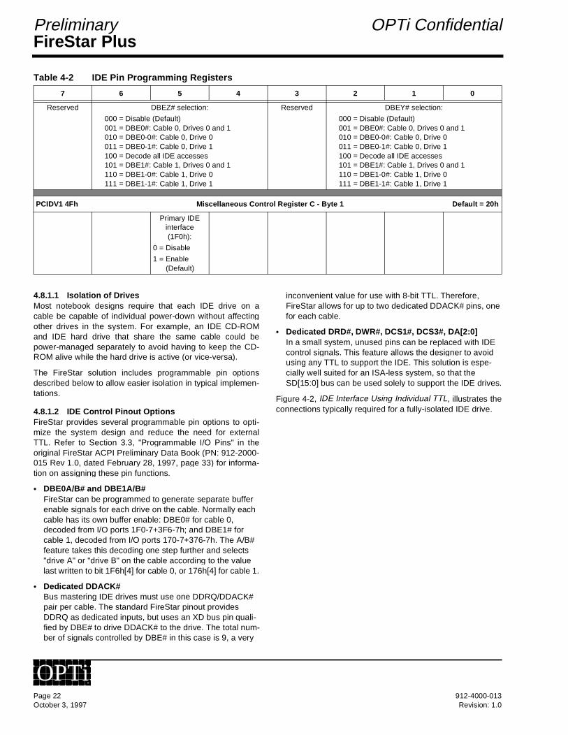
FireStar PlusPreliminary OPTi Confidential
4.8.1.1 Isolation of DrivesMost notebook designs require that each IDE drive on acable be capable of individual power-down without affectingother drives in the system. For example, an IDE CD-ROMand IDE hard drive that share the same cable could bepower-managed separately to avoid having to keep the CD-ROM alive while the hard drive is active (or vice-versa).
The FireStar solution includes programmable pin optionsdescribed below to allow easier isolation in typical implemen-tations.
4.8.1.2 IDE Control Pinout OptionsFireStar provides several programmable pin options to opti-mize the system design and reduce the need for externalTTL. Refer to Section 3.3, "Programmable I/O Pins" in theoriginal FireStar ACPI Preliminary Data Book (PN: 912-2000-015 Rev 1.0, dated February 28, 1997, page 33) for informa-tion on assigning these pin functions.
• DBE0A/B# and DBE1A/B#FireStar can be programmed to generate separate buffer enable signals for each drive on the cable. Normally each cable has its own buffer enable: DBE0# for cable 0, decoded from I/O ports 1F0-7+3F6-7h; and DBE1# for cable 1, decoded from I/O ports 170-7+376-7h. The A/B# feature takes this decoding one step further and selects "drive A" or "drive B" on the cable according to the value last written to bit 1F6h[4] for cable 0, or 176h[4] for cable 1.
• Dedicated DDACK#Bus mastering IDE drives must use one DDRQ/DDACK# pair per cable. The standard FireStar pinout provides DDRQ as dedicated inputs, but uses an XD bus pin quali-fied by DBE# to drive DDACK# to the drive. The total num-ber of signals controlled by DBE# in this case is 9, a very
inconvenient value for use with 8-bit TTL. Therefore, FireStar allows for up to two dedicated DDACK# pins, one for each cable.
• Dedicated DRD#, DWR#, DCS1#, DCS3#, DA[2:0]In a small system, unused pins can be replaced with IDE control signals. This feature allows the designer to avoid using any TTL to support the IDE. This solution is espe-cially well suited for an ISA-less system, so that the SD[15:0] bus can be used solely to support the IDE drives.
Figure 4-2, IDE Interface Using Individual TTL, illustrates theconnections typically required for a fully-isolated IDE drive.
Reserved DBEZ# selection:
000 = Disable (Default)001 = DBE0#: Cable 0, Drives 0 and 1010 = DBE0-0#: Cable 0, Drive 0011 = DBE0-1#: Cable 0, Drive 1100 = Decode all IDE accesses101 = DBE1#: Cable 1, Drives 0 and 1110 = DBE1-0#: Cable 1, Drive 0111 = DBE1-1#: Cable 1, Drive 1
Reserved DBEY# selection:
000 = Disable (Default)001 = DBE0#: Cable 0, Drives 0 and 1010 = DBE0-0#: Cable 0, Drive 0011 = DBE0-1#: Cable 0, Drive 1100 = Decode all IDE accesses101 = DBE1#: Cable 1, Drives 0 and 1110 = DBE1-0#: Cable 1, Drive 0111 = DBE1-1#: Cable 1, Drive 1
PCIDV1 4Fh Miscellaneous Control Register C - Byte 1 Default = 20h
Primary IDE interface (1F0h):
0 = Disable
1 = Enable (Default)
Table 4-2 IDE Pin Programming Registers
7 6 5 4 3 2 1 0
Page 22 912-4000-013October 3, 1997 Revision: 1.0
OPTi®

FireStar PlusOPTi Confidential Preliminary
Figure 4-2 IDE Interface Using Individual TTL
Figure 4-3, IDE Interface Using Zero-TTL, shows an imple-mentation for a minimal system without separately buffereddrives. A typical notebook design with few ISA-bus devicescould use this approach. Note that PIO pins have beenassigned IDE control functions DRD# and DWR# to allow azero-TTL solution, yet some of the control signals still comefrom the XD[7:0] bus. The X-bus control lines will also toggleduring cycles to the ROM, RTC, and KBC but will not have aneffect on the IDE drive since DRD# and DWR# are inactive. Ifthis situation is not acceptable and there are enough PIO pinsfree, all IDE control signals can be assigned to dedicatedpins. Table 4-3 list the general IDE control line assignment.
Figure 4-3 IDE Interface Using Zero-TTL
Table 4-3 General IDE Control Line Assignment
a. Should be used if UltraDMA is being used.
IOCHRDY
IOCHRDYDCHRDY
OE#DBE0#
244
DRD0#
DWR0#
DACK#
DA[2:0]
DCS1#
DCS3#
XD[7:0]
SD[15:0]
DD[15:0]
TC/IDEDIR
245
OE#
DIR
244
OE#
FireStarIDE
Controller
IDEDrive
Primary Pin Name IDE Signal Description
SD[15:0] DD[15:0] IDE data bus
XD7 DCS3# IDE chip select for 3F6-7h or 376-7h I/O access
XD6 DCS1# IDE chip select for 1F0-7h or 170-7h I/O access
XD5 DDACK# Bus master IDE DMA acknowledge
XD4 DA2 IDE address
XD3 DA1
XD2 DA0
XD1 DRD# IDE drive read command line, qualified by DBE#
XD0 DWR# IDE drive write command line, qualified by DBE#
Dedicated pin
DBE0# Command buffer enable to IDE cable 0
Dedicated pin
DDRQ0 Bus mastering IDE drive DMA request line for cable 0
PIO pin DBE1# Command buffer enable to IDE cable 1
PIO pin DDRQ1 Bus mastering IDE drive DMA request line for cable 1
TC IDEDIR Direction control for the IDE buff-ers.a
IOCHRDY DCHRDY
DRD#
DACK#
DA[2:0]
DCS1#
DCS3#
XD[7:0]
SD[15:0]
FireStarIDE
Controller
IDEDrive
DWR#
912-4000-013 Page 23Revision: 1.0 October 3, 1997
OPTi®

FireStar PlusPreliminary OPTi Confidential
4.8.2 Programming the IDE ControllerThe IDE controller has four register spaces that control it:
1. SYSCFG - SYSCFG registers are accessed by writingPort 022h with an index and writing or reading fromPort 024h with a data value.
2. PCIIDE - The PCIIDE space is accessed through PCIConfiguration Mechanism #1 by addressing Bus #0,Device #14h, Function #0.
3. IDE I/O - The IDE I/O space is a register set that is hid-den behind the IDE I/O ports, and is normally notaccessible. A special sequence must be followed forenabling/disabling access to these registers. Unlessotherwise noted, all references to IDE I/O space in thissection pertain to this hidden space. These configura-tion registers share the I/O ports.
4. Bus Master IDE registers - Mapped to system I/Ospace.
References to the IDE I/O space 1F0h-1F7h are used below.The same concepts apply to the 170h-177h space.
4.8.2.1 Enabling Access to IDE I/O SpaceTo enable access to the IDE I/O register space, the followingprocedure must be followed:
• Perform two consecutive 16-bit reads from I/O Port 1F1h. This operation makes the register space accessible for the next I/O operation.
• Perform an 8-bit write to I/O Port 1F2h with a value of 03h. This programming keeps the registers accessible indefi-nitely.
4.8.2.2 Disabling Access to IDE I/O SpaceAfter enabling and programming the IDE I/O registers, theseregisters must be hidden from standard access before IDEoperations can begin. Two options are available:
• Write Port 1F2h with a value of C3h to disable the IDE I/O register space and fully enable IDE operation, and also prevent any future access to this space until the next hard-ware reset.
• Write Port 1F2h with a value of 83h to disable the IDE I/O space and fully enable IDE operation, but leave open the future possibility of accessing this space by enabling the space again as previously described in Section 4.8.2.1, "Enabling Access to IDE I/O Space".
Table 4-4 shows the registers associated with enabling anddisabling access to the IDE I/O space.
Table 4-4 Enabling/Disabling Access to IDE I/O Space Registers
7 6 5 4 3 2 1 0
I/O Address 1F1h Write Cycle Timing Register - Timing 0 (1) Default = xxh
Write pulse width:
The value programmed in this register plus one determines the DWR# pulse width in PCICLKs (for a 16-bit write from the IDE Data Register). See Table 4-9 or Table 4-10.
(Default = xxxx)
Write recovery time:
The value programmed in this register plus two determines the recov-ery time between the end of DWR# and the next DA[2:0]/DCSx# being presented (after a 16-bit write from the IDE Data Register), measured in PCICLKs. See Table 4-9 or Table 4-10.
(Default = xxxx)
(1) Timing 0 can be programmed only if IDE I/O 1F6h[0] = 0. The timing programmed into this register is applied for IDE accesses to drives as selected by 1F3h[3:2] and 1F3h[7].
I/O Address 1F1h Write Cycle Timing Register - Timing 1 (1) Default = xxh
Write pulse width:
The value programmed in this register plus one determines the DWR# pulse width in PCICLKs (for a 16-bit write from the IDE Data Register). See Table 4-9 or Table 4-10.
(Default = xxxx)
Write recovery time:
The value programmed in this register plus two determines the recov-ery time between the end of DWR# and the next DA[2:0]/DCSx# being presented (after a 16-bit write from the IDE Data Register), measured in PCICLKs. See Table 4-9 or Table 4-10.
(Default = xxxx)
(1) Timing 1 can be programmed only if IDE I/O 1F6h[0] = 1. The timing programmed into this register is applied for IDE accesses to drives as selected by 1F3h[3:2] and 1F3h[7].
Page 24 912-4000-013October 3, 1997 Revision: 1.0
OPTi®
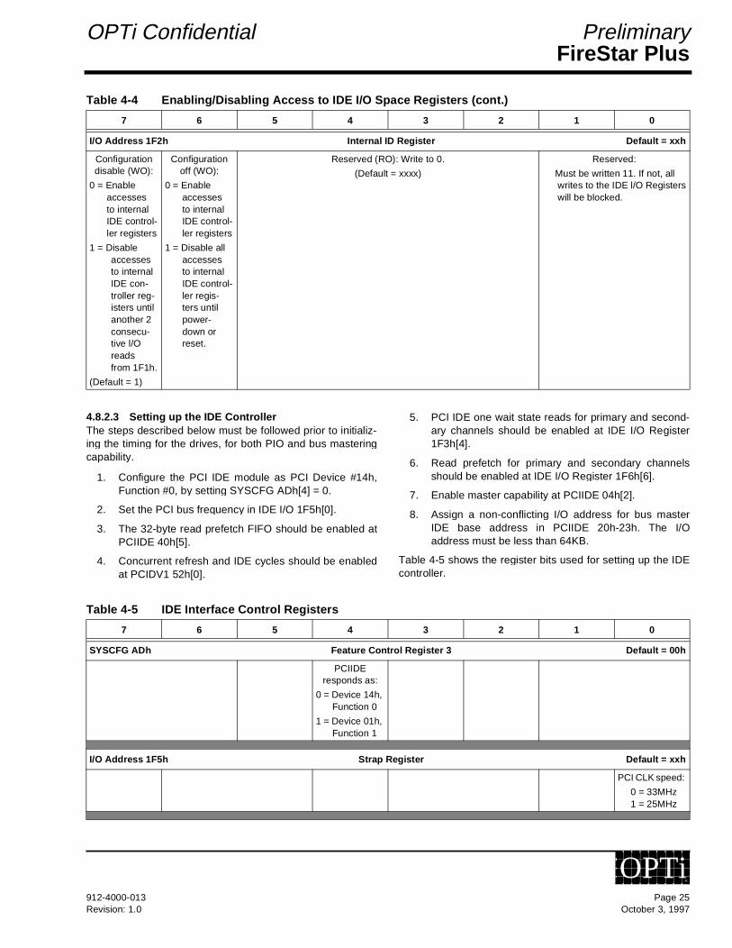
FireStar PlusOPTi Confidential Preliminary
4.8.2.3 Setting up the IDE ControllerThe steps described below must be followed prior to initializ-ing the timing for the drives, for both PIO and bus masteringcapability.
1. Configure the PCI IDE module as PCI Device #14h,Function #0, by setting SYSCFG ADh[4] = 0.
2. Set the PCI bus frequency in IDE I/O 1F5h[0].
3. The 32-byte read prefetch FIFO should be enabled atPCIIDE 40h[5].
4. Concurrent refresh and IDE cycles should be enabledat PCIDV1 52h[0].
5. PCI IDE one wait state reads for primary and second-ary channels should be enabled at IDE I/O Register1F3h[4].
6. Read prefetch for primary and secondary channelsshould be enabled at IDE I/O Register 1F6h[6].
7. Enable master capability at PCIIDE 04h[2].
8. Assign a non-conflicting I/O address for bus masterIDE base address in PCIIDE 20h-23h. The I/Oaddress must be less than 64KB.
Table 4-5 shows the register bits used for setting up the IDEcontroller.
I/O Address 1F2h Internal ID Register Default = xxh
Configuration disable (WO):
0 = Enable accesses to internal IDE control-ler registers
1 = Disable accesses to internal IDE con-troller reg-isters until another 2 consecu-tive l/O reads from 1F1h.
(Default = 1)
Configuration off (WO):
0 = Enable accesses to internal IDE control-ler registers
1 = Disable all accesses to internal IDE control-ler regis-ters until power-down or reset.
Reserved (RO): Write to 0.
(Default = xxxx)
Reserved:
Must be written 11. If not, all writes to the IDE l/O Registers will be blocked.
Table 4-4 Enabling/Disabling Access to IDE I/O Space Registers (cont.)
7 6 5 4 3 2 1 0
Table 4-5 IDE Interface Control Registers
7 6 5 4 3 2 1 0
SYSCFG ADh Feature Control Register 3 Default = 00h
PCIIDE responds as:
0 = Device 14h, Function 0
1 = Device 01h, Function 1
I/O Address 1F5h Strap Register Default = xxh
PCI CLK speed:
0 = 33MHz1 = 25MHz
912-4000-013 Page 25Revision: 1.0 October 3, 1997
OPTi®

FireStar PlusPreliminary OPTi Confidential
PCIIDE 40h IDE Initialization Control Register Default = 00h
Enhanced Slave:
0 = 82C621A-compatible mode, uses a 16-byte FIFO in PIO Mode
1 = Enhanced mode, uses a 32-byte FIFO in PIO Mode
Secondary IDE:
0 = Enable1 = Disable
This bit is effec-tive only if PCIDV1 4Fh[6] = 1.
PCIDV1 52h Misc. Controller Register 3 Default = 00h
Concurrent refresh and IDE cycle:
0 = Disable1 = Enable
ISA devices that rely on accu-rate refresh addresses for proper opera-tion should dis-able this bit.
I/O Address 1F3h Control Register Default = xxh
Enable one wait state read:
0 = 2 WS minimum
1 = 1 WS minimum for data reads
I/O Address 1F6h Miscellaneous Register Default = xxh
Read prefetch:
0 = Disable1 = Enable
Table 4-5 IDE Interface Control Registers (cont.)
7 6 5 4 3 2 1 0
Page 26 912-4000-013October 3, 1997 Revision: 1.0
OPTi®
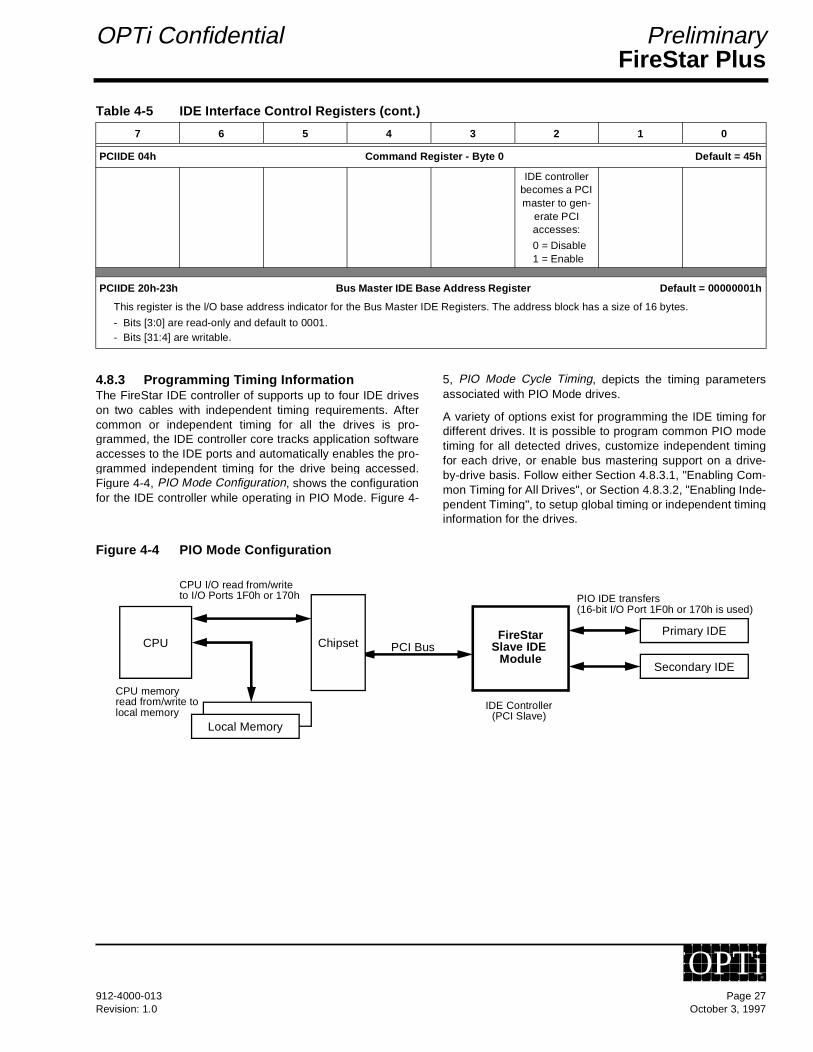
FireStar PlusOPTi Confidential Preliminary
4.8.3 Programming Timing InformationThe FireStar IDE controller of supports up to four IDE driveson two cables with independent timing requirements. Aftercommon or independent timing for all the drives is pro-grammed, the IDE controller core tracks application softwareaccesses to the IDE ports and automatically enables the pro-grammed independent timing for the drive being accessed.Figure 4-4, PIO Mode Configuration, shows the configurationfor the IDE controller while operating in PIO Mode. Figure 4-
5, PIO Mode Cycle Timing, depicts the timing parametersassociated with PIO Mode drives.
A variety of options exist for programming the IDE timing fordifferent drives. It is possible to program common PIO modetiming for all detected drives, customize independent timingfor each drive, or enable bus mastering support on a drive-by-drive basis. Follow either Section 4.8.3.1, "Enabling Com-mon Timing for All Drives", or Section 4.8.3.2, "Enabling Inde-pendent Timing", to setup global timing or independent timinginformation for the drives.
Figure 4-4 PIO Mode Configuration
PCIIDE 04h Command Register - Byte 0 Default = 45h
IDE controller becomes a PCI master to gen-
erate PCI accesses:
0 = Disable1 = Enable
PCIIDE 20h-23h Bus Master IDE Base Address Register Default = 00000001h
This register is the l/O base address indicator for the Bus Master IDE Registers. The address block has a size of 16 bytes.
- Bits [3:0] are read-only and default to 0001. - Bits [31:4] are writable.
Table 4-5 IDE Interface Control Registers (cont.)
7 6 5 4 3 2 1 0
CPU
Local Memory
PCI BusFireStar
Slave IDE
Secondary IDE
Primary IDE
CPU I/O read from/write to I/O Ports 1F0h or 170h
Chipset
PIO IDE transfers(16-bit I/O Port 1F0h or 170h is used)
Module
CPU memoryread from/write tolocal memory
IDE Controller(PCI Slave)
912-4000-013 Page 27Revision: 1.0 October 3, 1997
OPTi®

FireStar PlusPreliminary OPTi Confidential
Figure 4-5 PIO Mode Cycle Timing
4.8.3.1 Enabling Common Timing for All DrivesTable 4-6 shows the registers associated with programmingcommon timing for all enabled drives. Common IDE timing forall drives is enabled by the IDE controller until independenttiming is programmed.
The default common timing for all drives is PIO Mode 0. Com-mon PIO Modes 0-3 timing for all enabled drives can be pro-grammed by setting PCIIDE 40h[1:0].
To enable common PIO Mode 4 or Mode 5 timing, firstensure that PIO Mode 3 is set up in PCIIDE 40h[1:0], asdescribed above. Subsequently, the appropriate bits in PCI-IDE 43h[7:0] can be set to enable Mode 4 or Mode 5 timing.
DA[2:0],
DRD#/DWR#
DD[15:0]
Address Setup Command Pulse
Cycle Time
Command Recovery
DCS1#, DCS3#
Table 4-6 IDE Timing Control “Common Timing”
7 6 5 4 3 2 1 0
PCIIDE 40h IDE Initialization Control Register Default = 00h
Mode:
These bits control the default 16-bit cycle times for all IDE
devices and can be overridden by programming the IDE I/O
Registers.
00 = > 600ns cycle time (PIO Mode 0)
01 = > 383ns cycle time (PIO Mode 2)
10 = > 240ns cycle time (PIO Mode 1)
11 = > 180ns cycle time (PIO Mode 3)
These bits are effective only if PCIDV1 4Fh[6] = 1.
Page 28 912-4000-013October 3, 1997 Revision: 1.0
OPTi®
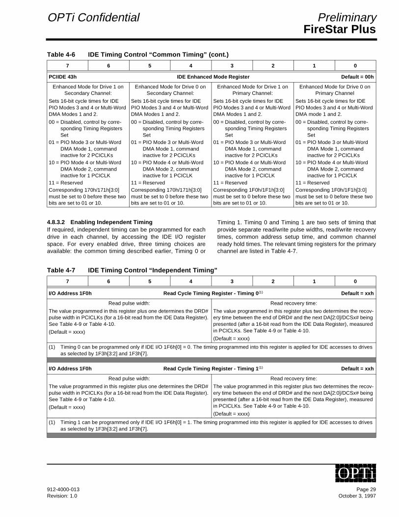
FireStar PlusOPTi Confidential Preliminary
4.8.3.2 Enabling Independent TimingIf required, independent timing can be programmed for eachdrive in each channel, by accessing the IDE I/O registerspace. For every enabled drive, three timing choices areavailable: the common timing described earlier, Timing 0 or
Timing 1. Timing 0 and Timing 1 are two sets of timing thatprovide separate read/write pulse widths, read/write recoverytimes, common address setup time, and common channelready hold times. The relevant timing registers for the primarychannel are listed in Table 4-7.
PCIIDE 43h IDE Enhanced Mode Register Default = 00h
Enhanced Mode for Drive 1 on Secondary Channel:
Sets 16-bit cycle times for IDE PIO Modes 3 and 4 or Multi-Word DMA Modes 1 and 2.
00 = Disabled, control by corre-sponding Timing Registers Set
01 = PIO Mode 3 or Multi-Word DMA Mode 1, command inactive for 2 PCICLKs
10 = PIO Mode 4 or Multi-Word DMA Mode 2, command inactive for 1 PCICLK
11 = ReservedCorresponding 170h/171h[3:0] must be set to 0 before these two bits are set to 01 or 10.
Enhanced Mode for Drive 0 on Secondary Channel:
Sets 16-bit cycle times for IDE PIO Modes 3 and 4 or Multi-Word DMA Modes 1 and 2.
00 = Disabled, control by corre-sponding Timing Registers Set
01 = PIO Mode 3 or Multi-Word DMA Mode 1, command inactive for 2 PCICLKs
10 = PIO Mode 4 or Multi-Word DMA Mode 2, command inactive for 1 PCICLK
11 = ReservedCorresponding 170h/171h[3:0] must be set to 0 before these two bits are set to 01 or 10.
Enhanced Mode for Drive 1 on Primary Channel:
Sets 16-bit cycle times for IDE PIO Modes 3 and 4 or Multi-Word DMA Modes 1 and 2.
00 = Disabled, control by corre-sponding Timing Registers Set
01 = PIO Mode 3 or Multi-Word DMA Mode 1, command inactive for 2 PCICLKs
10 = PIO Mode 4 or Multi-Word DMA Mode 2, command inactive for 1 PCICLK
11 = ReservedCorresponding 1F0h/1F1h[3:0] must be set to 0 before these two bits are set to 01 or 10.
Enhanced Mode for Drive 0 on Primary Channel
Sets 16-bit cycle times for IDE PIO Modes 3 and 4 or Multi-Word DMA mode 1 and 2.
00 = Disabled, control by corre-sponding Timing Registers Set
01 = PIO Mode 3 or Multi-Word DMA Mode 1, command inactive for 2 PCICLKs
10 = PIO Mode 4 or Multi-Word DMA Mode 2, command inactive for 1 PCICLK
11 = ReservedCorresponding 1F0h/1F1h[3:0] must be set to 0 before these two bits are set to 01 or 10.
Table 4-6 IDE Timing Control “Common Timing” (cont.)
7 6 5 4 3 2 1 0
Table 4-7 IDE Timing Control “Independent Timing”
7 6 5 4 3 2 1 0
I/O Address 1F0h Read Cycle Timing Register - Timing 0 (1) Default = xxh
Read pulse width:
The value programmed in this register plus one determines the DRD# pulse width in PCICLKs (for a 16-bit read from the IDE Data Register). See Table 4-9 or Table 4-10.
(Default = xxxx)
Read recovery time:
The value programmed in this register plus two determines the recov-ery time between the end of DRD# and the next DA[2:0]/DCSx# being presented (after a 16-bit read from the IDE Data Register), measured in PCICLKs. See Table 4-9 or Table 4-10.
(Default = xxxx)
(1) Timing 0 can be programmed only if IDE I/O 1F6h[0] = 0. The timing programmed into this register is applied for IDE accesses to drives as selected by 1F3h[3:2] and 1F3h[7].
I/O Address 1F0h Read Cycle Timing Register - Timing 1 (1) Default = xxh
Read pulse width:
The value programmed in this register plus one determines the DRD# pulse width in PCICLKs (for a 16-bit read from the IDE Data Register). See Table 4-9 or Table 4-10.
(Default = xxxx)
Read recovery time:
The value programmed in this register plus two determines the recov-ery time between the end of DRD# and the next DA[2:0]/DCSx# being presented (after a 16-bit read from the IDE Data Register), measured in PCICLKs. See Table 4-9 or Table 4-10.
(Default = xxxx)
(1) Timing 1 can be programmed only if IDE I/O 1F6h[0] = 1. The timing programmed into this register is applied for IDE accesses to drives as selected by 1F3h[3:2] and 1F3h[7].
912-4000-013 Page 29Revision: 1.0 October 3, 1997
OPTi®

FireStar PlusPreliminary OPTi Confidential
I/O Address 1F1h Write Cycle Timing Register - Timing 0 (1) Default = xxh
Write pulse width:
The value programmed in this register plus one determines the DWR# pulse width in PCICLKs (for a 16-bit write from the IDE Data Register). See Table 4-9 or Table 4-10.
(Default = xxxx)
Write recovery time:
The value programmed in this register plus two determines the recov-ery time between the end of DWR# and the next DA[2:0]/DCSx# being presented (after a 16-bit write from the IDE Data Register), measured in PCICLKs. See Table 4-9 or Table 4-10.
(Default = xxxx)
(1) Timing 0 can be programmed only if IDE I/O 1F6h[0] = 0. The timing programmed into this register is applied for IDE accesses to drives as selected by 1F3h[3:2] and 1F3h[7].
I/O Address 1F1h Write Cycle Timing Register - Timing 1 (1) Default = xxh
Write pulse width:
The value programmed in this register plus one determines the DWR# pulse width in PCICLKs (for a 16-bit write from the IDE Data Register). See Table 4-9 or Table 4-10.
(Default = xxxx)
Write recovery time:
The value programmed in this register plus two determines the recov-ery time between the end of DWR# and the next DA[2:0]/DCSx# being presented (after a 16-bit write from the IDE Data Register), measured in PCICLKs. See Table 4-9 or Table 4-10.
(Default = xxxx)
(1) Timing 1 can be programmed only if IDE I/O 1F6h[0] = 1. The timing programmed into this register is applied for IDE accesses to drives as selected by 1F3h[3:2] and 1F3h[7].
Note: Both Timing 0 and Timing 1 sets share the same address setup and DRDY delay times as programmed in 1F6h[5:4] and 1F6h[3:2].
I/O Address 1F3h Control Register Default = xxh
Timing register value select:
0 = Basic1 = Enhanced
Drive 1 timing select:
Basic (1F3h[7] = 0):
0 = Determined by PCIIDE 40h[1:0]
1 = Timing 1
Enhanced (1F3h[7] = 1):
0 = Timing 11 = Timing 0
Drive 0 timing select:
Basic(1F3h[7] = 0):
0 = Determined by PCIIDE 40h[1:0]
1 = Timing 1
Enhanced (1F3h[7] = 1):
0 = Timing 11 = Timing 0
Note: Bits 2, 3 and 7 of the Control Register should be enabled after the Cycle Timing Registers and Miscellaneous Register are pro-grammed. See Table 4-8 for programming options.
I/O Address 1F6h Miscellaneous Register Default = xxh
Address setup time:(1)
The value programmed in this register plus one determines the address setup time between DRD# or DWR# going active and DA[2:0], DCS3#, DCS1# being presented, measured in PCI-CLKs. See Table 4-9 or Table 4-10.
(Default = xx)
Delay:(1)
The value programmed in this register plus two determines the minimum number of PCICLKs between DRDY# going high and DRD# or DWR# going inactive. See Table 4-9 or Table 4-10.
(Default = xxx)
Timing register load select:
0 = Timing 0(1F0-1F1h accept Tim-ing 0 val-ues)
1 = Timing 1(1F0-1F1h accept Tim-ing 1 val-ues)
(1) Both Timing 0 and Timing 1 sets have common address setup and DRDY delay times as programmed in 1F6h[5:2].
Table 4-7 IDE Timing Control “Independent Timing” (cont.)
7 6 5 4 3 2 1 0
Page 30 912-4000-013October 3, 1997 Revision: 1.0
OPTi®

FireStar PlusOPTi Confidential Preliminary
Setting up independent timing for drives is a two step pro-cess. The first step is to load the timing information sets(common, Timing 0, Timing 1). The second step is to associ-ate each drive with one of the preloaded timing sets. Figure4-6, IDE Interface Primary Channel Programming Flow Chart,is a flow chart that describes how to program the drives of the
primary channel of the IDE interface with independent timingrequirements, for the configuration recommended in Table 4-8. For the secondary channel, a similar procedure can be fol-lowed by changing all the indexes from 1Fxh to 17xh, andprogramming PCIIDE 43h[7:4].
Figure 4-6 IDE Interface Primary Channel Programming Flow Chart
4.8.3.3 Loading Timing 0 and Timing 1 sets:The parameters for Timing 0 are programmed by first settingIDE I/O 1F6h[0] = 0, followed by initializing IDE I/O 1F0h and1F1h with the first set of read/write pulse widths and read/write recovery times. The parameters for Timing 1 are pro-grammed by first setting IDE I/O 1F6h[0] = 1, followed by ini-tializing IDE I/O 1F0h and 1F1h with a second set of read/write pulse widths and read/write recovery times.
Address setup time and channel ready hold time (DRDY) arecommon to both timing sets and are programmed in1F6h[5:4] and 1F6h[3:1] respectively. Refer to Table 4-9 andTable 4-10 for information regarding the values that need tobe programmed in the timing registers for different modes.
4.8.3.4 Associating drives with timing sets:Each enabled drive can be associated with one of the pre-loaded timings according to Table 4-8, by programming IDE I/O registers 1F3h[7] and 1F3h[3:2] (these must be pro-grammed after setting up the timing sets. For every enableddrive, the IDE controller allows two basic choices for timingcontrol, “Basic”, or “Enhanced”, depending on the value ofIDE I/O register 1F3h[7].
“Basic” choices (IDE I/O 1F3h[7] = 0): 1. The “common” timings as described in Section 4.8.3.1,
"Enabling Common Timing for All Drives", where tim-ing for all drives is determined by PCIIDE 40h[1:0](Modes 0-3), or PCIIDE 43h[7:0] (Modes 4-5).
Enter the IDE I/O Registers Programming Mode: Two consecutive (any other I/O cycle between these two reads will disable access to the IDE registers) 16-bit I/O reads from 1F1h followed by an 8-bit I/O write to 1F2h with a value of 03h.
Set the values for Timing 0:1) Write 0 to 1F6[0] to load Timing 0 parameters.2) First set proper values in registers 1F0h and 1F1h for read/write pulse width and recovery times, and then program PCIIDE
43h[1:0], according to Table 4-9 or Table 4-10. (Program PCIIDE 43h[5:4] for Drive 0 of secondary channel).
Set the values for Timing 1:1) Write 1 to 1F6[0] to load Timing 1 parameters.2) First set proper values in registers 1F0h and 1F1h for read/write pulse width and recovery times, and then program PCIIDE
43h[3:2], according to Table 4-9 or Table 4-10. (Program PCIIDE 43h[7:6] for Drive 1 of secondary channel).
Program the Address Setup Time and DRDY Delay Time:1) Follow Table 4-9 or Table 4-10 to set proper values into registers 1F6h[5:4]. Reset 1F6h[3:1] to 0.2) The address setup time and DRDY delay time are common to both Timing 0 and Timing 1. If they are not the same mode, program
the slower timings for the address setup time.
Associate the drives with Common timings, Timing 0 parameters, or Timing 1 parameters: Follow Table 4-8 to set proper values in the registers 1F3h[7,3,2]. This should be done after all the read/write pulse and recovery, address setup, and DRDY delay have been set.
Exit the IDE I/O Registers Programming Mode: An 8-bit I/O write to 1F2h with a value of 83h.
912-4000-013 Page 31Revision: 1.0 October 3, 1997
OPTi®
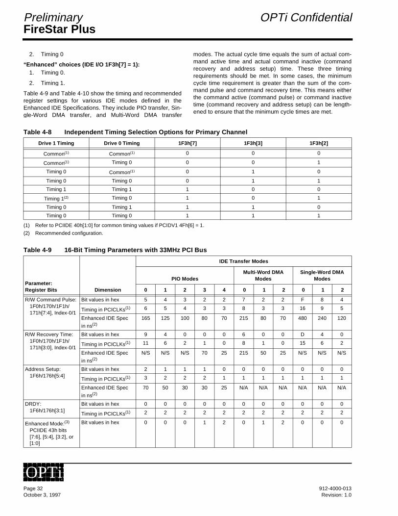
FireStar PlusPreliminary OPTi Confidential
2. Timing 0
“Enhanced” choices (IDE I/O 1F3h[7] = 1):1. Timing 0.
2. Timing 1.
Table 4-9 and Table 4-10 show the timing and recommendedregister settings for various IDE modes defined in theEnhanced IDE Specifications. They include PIO transfer, Sin-gle-Word DMA transfer, and Multi-Word DMA transfer
modes. The actual cycle time equals the sum of actual com-mand active time and actual command inactive (commandrecovery and address setup) time. These three timingrequirements should be met. In some cases, the minimumcycle time requirement is greater than the sum of the com-mand pulse and command recovery time. This means eitherthe command active (command pulse) or command inactivetime (command recovery and address setup) can be length-ened to ensure that the minimum cycle times are met.
Table 4-8 Independent Timing Selection Options for Primary Channel
(1) Refer to PCIIDE 40h[1:0] for common timing values if PCIDV1 4Fh[6] = 1.
(2) Recommended configuration.
Table 4-9 16-Bit Timing Parameters with 33MHz PCI Bus
Drive 1 Timing Drive 0 Timing 1F3h[7] 1F3h[3] 1F3h[2]
Common(1) Common(1) 0 0 0
Common(1) Timing 0 0 0 1
Timing 0 Common(1) 0 1 0
Timing 0 Timing 0 0 1 1
Timing 1 Timing 1 1 0 0
Timing 1(2) Timing 0 1 0 1
Timing 0 Timing 1 1 1 0
Timing 0 Timing 0 1 1 1
Parameter: Register Bits Dimension
IDE Transfer Modes
PIO ModesMulti-Word DMA
ModesSingle-Word DMA
Modes
0 1 2 3 4 0 1 2 0 1 2
R/W Command Pulse:1F0h/170h/1F1h/171h[7:4], Index-0/1
Bit values in hex 5 4 3 2 2 7 2 2 F 8 4
Timing in PCICLKs(1) 6 5 4 3 3 8 3 3 16 9 5
Enhanced IDE Spec
in ns(2)165 125 100 80 70 215 80 70 480 240 120
R/W Recovery Time:1F0h/170h/1F1h/171h[3:0], Index-0/1
Bit values in hex 9 4 0 0 0 6 0 0 D 4 0
Timing in PCICLKs(1) 11 6 2 1 0 8 1 0 15 6 2
Enhanced IDE Spec
in ns(2)N/S N/S N/S 70 25 215 50 25 N/S N/S N/S
Address Setup:1F6h/176h[5:4]
Bit values in hex 2 1 1 1 0 0 0 0 0 0 0
Timing in PCICLKs(1) 3 2 2 2 1 1 1 1 1 1 1
Enhanced IDE Spec
in ns(2)70 50 30 30 25 N/A N/A N/A N/A N/A N/A
DRDY:1F6h/176h[3:1]
Bit values in hex 0 0 0 0 0 0 0 0 0 0 0
Timing in PCICLKs(1) 2 2 2 2 2 2 2 2 2 2 2
Enhanced Mode:(3)
PCIIDE 43h bits [7:6], [5:4], [3:2], or [1:0]
Bit values in hex 0 0 0 1 2 0 1 2 0 0 0
Page 32 912-4000-013October 3, 1997 Revision: 1.0
OPTi®
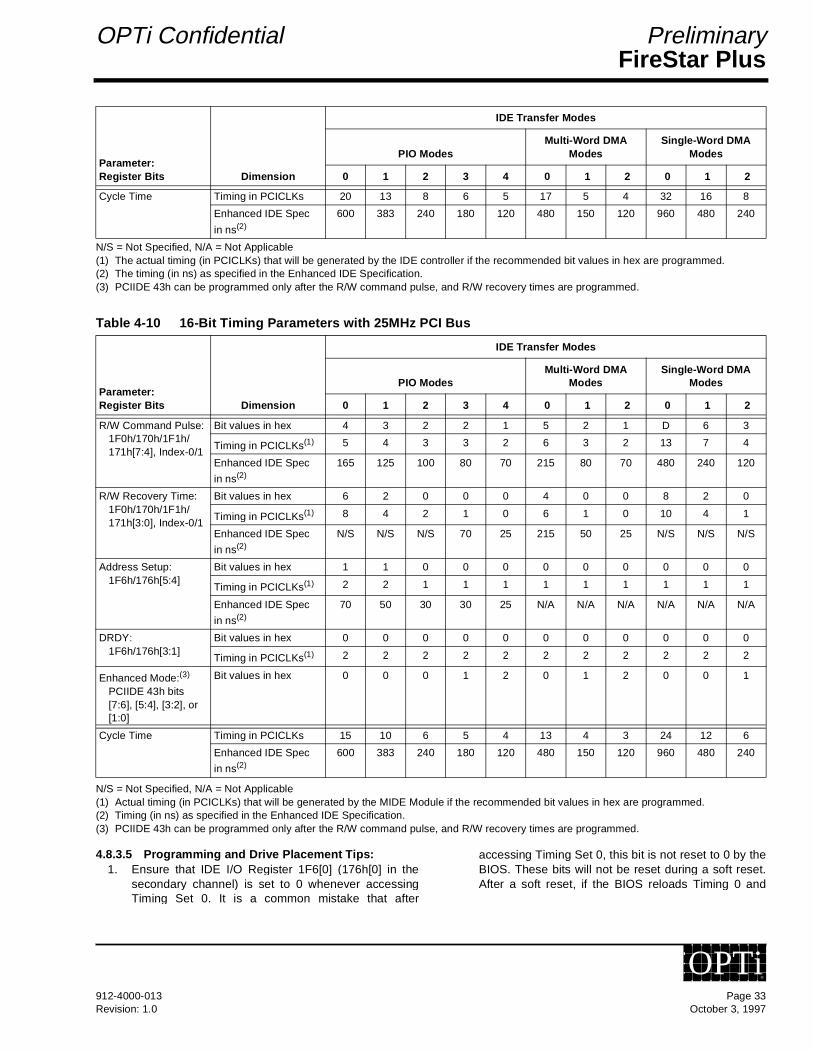
FireStar PlusOPTi Confidential Preliminary
N/S = Not Specified, N/A = Not Applicable(1) The actual timing (in PCICLKs) that will be generated by the IDE controller if the recommended bit values in hex are programmed.(2) The timing (in ns) as specified in the Enhanced IDE Specification. (3) PCIIDE 43h can be programmed only after the R/W command pulse, and R/W recovery times are programmed.
Table 4-10 16-Bit Timing Parameters with 25MHz PCI Bus
N/S = Not Specified, N/A = Not Applicable(1) Actual timing (in PCICLKs) that will be generated by the MIDE Module if the recommended bit values in hex are programmed.(2) Timing (in ns) as specified in the Enhanced IDE Specification. (3) PCIIDE 43h can be programmed only after the R/W command pulse, and R/W recovery times are programmed.
4.8.3.5 Programming and Drive Placement Tips:1. Ensure that IDE I/O Register 1F6[0] (176h[0] in the
secondary channel) is set to 0 whenever accessingTiming Set 0. It is a common mistake that after
accessing Timing Set 0, this bit is not reset to 0 by theBIOS. These bits will not be reset during a soft reset.After a soft reset, if the BIOS reloads Timing 0 and
Cycle Time Timing in PCICLKs 20 13 8 6 5 17 5 4 32 16 8
Enhanced IDE Spec
in ns(2)600 383 240 180 120 480 150 120 960 480 240
Parameter: Register Bits Dimension
IDE Transfer Modes
PIO ModesMulti-Word DMA
ModesSingle-Word DMA
Modes
0 1 2 3 4 0 1 2 0 1 2
R/W Command Pulse:1F0h/170h/1F1h/171h[7:4], Index-0/1
Bit values in hex 4 3 2 2 1 5 2 1 D 6 3
Timing in PCICLKs(1) 5 4 3 3 2 6 3 2 13 7 4
Enhanced IDE Spec
in ns(2)165 125 100 80 70 215 80 70 480 240 120
R/W Recovery Time:1F0h/170h/1F1h/171h[3:0], Index-0/1
Bit values in hex 6 2 0 0 0 4 0 0 8 2 0
Timing in PCICLKs(1) 8 4 2 1 0 6 1 0 10 4 1
Enhanced IDE Spec
in ns(2)N/S N/S N/S 70 25 215 50 25 N/S N/S N/S
Address Setup:1F6h/176h[5:4]
Bit values in hex 1 1 0 0 0 0 0 0 0 0 0
Timing in PCICLKs(1) 2 2 1 1 1 1 1 1 1 1 1
Enhanced IDE Spec
in ns(2)70 50 30 30 25 N/A N/A N/A N/A N/A N/A
DRDY:1F6h/176h[3:1]
Bit values in hex 0 0 0 0 0 0 0 0 0 0 0
Timing in PCICLKs(1) 2 2 2 2 2 2 2 2 2 2 2
Enhanced Mode:(3)
PCIIDE 43h bits [7:6], [5:4], [3:2], or [1:0]
Bit values in hex 0 0 0 1 2 0 1 2 0 0 1
Cycle Time Timing in PCICLKs 15 10 6 5 4 13 4 3 24 12 6
Enhanced IDE Spec
in ns(2)600 383 240 180 120 480 150 120 960 480 240
Parameter: Register Bits Dimension
IDE Transfer Modes
PIO ModesMulti-Word DMA
ModesSingle-Word DMA
Modes
0 1 2 3 4 0 1 2 0 1 2
912-4000-013 Page 33Revision: 1.0 October 3, 1997
OPTi®
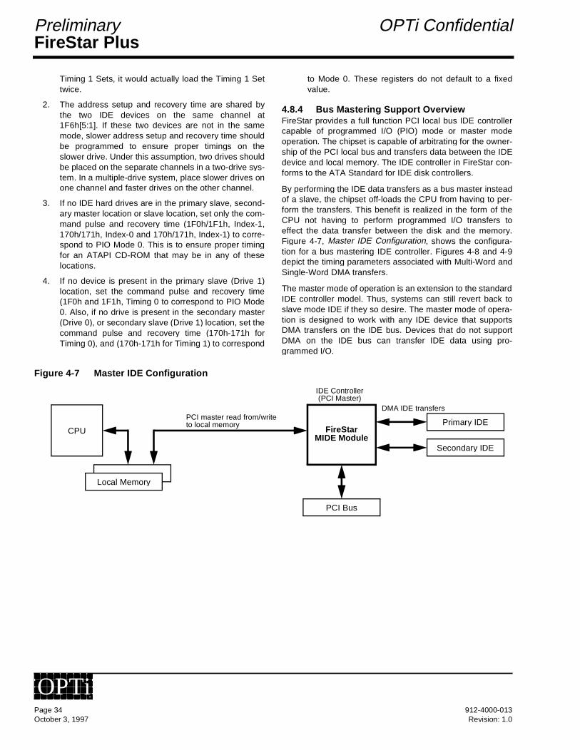
FireStar PlusPreliminary OPTi Confidential
Timing 1 Sets, it would actually load the Timing 1 Settwice.
2. The address setup and recovery time are shared bythe two IDE devices on the same channel at1F6h[5:1]. If these two devices are not in the samemode, slower address setup and recovery time shouldbe programmed to ensure proper timings on theslower drive. Under this assumption, two drives shouldbe placed on the separate channels in a two-drive sys-tem. In a multiple-drive system, place slower drives onone channel and faster drives on the other channel.
3. If no IDE hard drives are in the primary slave, second-ary master location or slave location, set only the com-mand pulse and recovery time (1F0h/1F1h, Index-1,170h/171h, Index-0 and 170h/171h, Index-1) to corre-spond to PIO Mode 0. This is to ensure proper timingfor an ATAPI CD-ROM that may be in any of theselocations.
4. If no device is present in the primary slave (Drive 1)location, set the command pulse and recovery time(1F0h and 1F1h, Timing 0 to correspond to PIO Mode0. Also, if no drive is present in the secondary master(Drive 0), or secondary slave (Drive 1) location, set thecommand pulse and recovery time (170h-171h forTiming 0), and (170h-171h for Timing 1) to correspond
to Mode 0. These registers do not default to a fixedvalue.
4.8.4 Bus Mastering Support Overview FireStar provides a full function PCI local bus IDE controllercapable of programmed I/O (PIO) mode or master modeoperation. The chipset is capable of arbitrating for the owner-ship of the PCI local bus and transfers data between the IDEdevice and local memory. The IDE controller in FireStar con-forms to the ATA Standard for IDE disk controllers.
By performing the IDE data transfers as a bus master insteadof a slave, the chipset off-loads the CPU from having to per-form the transfers. This benefit is realized in the form of theCPU not having to perform programmed I/O transfers toeffect the data transfer between the disk and the memory.Figure 4-7, Master IDE Configuration, shows the configura-tion for a bus mastering IDE controller. Figures 4-8 and 4-9depict the timing parameters associated with Multi-Word andSingle-Word DMA transfers.
The master mode of operation is an extension to the standardIDE controller model. Thus, systems can still revert back toslave mode IDE if they so desire. The master mode of opera-tion is designed to work with any IDE device that supportsDMA transfers on the IDE bus. Devices that do not supportDMA on the IDE bus can transfer IDE data using pro-grammed I/O.
Figure 4-7 Master IDE Configuration
CPU
Local Memory
FireStarMIDE Module
Secondary IDE
Primary IDEPCI master read from/write to local memory
DMA IDE transfers
IDE Controller(PCI Master)
PCI Bus
Page 34 912-4000-013October 3, 1997 Revision: 1.0
OPTi®
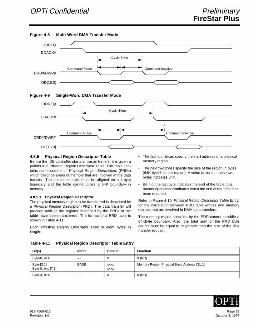
FireStar PlusOPTi Confidential Preliminary
Figure 4-8 Multi-Word DMA Transfer Mode
Figure 4-9 Single-Word DMA Transfer Mode
4.8.5 Physical Region Descriptor TableBefore the IDE controller starts a master transfer it is given apointer to a Physical Region Descriptor Table. This table con-tains some number of Physical Region Descriptors (PRDs)which describe areas of memory that are involved in the datatransfer. The descriptor table must be aligned on a 4-byteboundary and the table cannot cross a 64K boundary inmemory.
4.8.5.1 Physical Region DescriptorThe physical memory region to be transferred is described bya Physical Region Descriptor (PRD). The data transfer willproceed until all the regions described by the PRDs in thetable have been transferred. The format of a PRD table isshown in Table 4-11.
Each Physical Region Descriptor entry is eight bytes inlength:
• The first four bytes specify the start address of a physical memory region.
• The next two bytes specify the size of the region in bytes (64K byte limit per region). A value of zero in these two bytes indicates 64K.
• Bit 7 of the last byte indicates the end of the table; bus master operation terminates when the end of the table has been reached.
Refer to Figure 4-10, Physical Region Descriptor Table Entry,for the correlation between PRD table entries and memoryregions that are involved in DMA data transfers.
The memory region specified by the PRD cannot straddle a64Kbyte boundary. Also, the total sum of the PRD bytecounts must be equal to or greater than the size of the disktransfer request.
Table 4-11 Physical Region Descriptor Table Entry
DDREQ
DDACK#
DRD#/DWR#
DD[15:0]
Command Pulse Command Inactive
Cycle Time
DDREQ
DDACK#
DRD#/DWR#
DD[15:0]
Command Pulse Command Inactive
Cycle Time
Bit(s) Name Default Function
Byte-0, bit 0 --- 0 0 (RO)
Byte-[3:1]Byte-0, bits [7:1]
BASE xxxxxxxx
Memory Region Physical Base Address [31:1]
Byte-4, bit 0 --- 0 0 (RO)
912-4000-013 Page 35Revision: 1.0 October 3, 1997
OPTi®

FireStar PlusPreliminary OPTi Confidential
Note: The memory region specified by the descriptor is further restricted such that the region cannot straddle a 64K boundary. This means the byte count is limited to 64K and the incrementer for the current address register only extends from bit 1 to bit 15.
Figure 4-10 Physical Region Descriptor Table Entry
4.8.5.2 Bus Master IDE RegistersThe bus master IDE function uses 16 bytes of l/O space. Thebase address of this block of l/O space is pointed to by theBus Master IDE Base Address Register and PCIIDE 20h-23h. All bus master IDE l/O space registers can be accessedas byte, word, or dword quantities. The description of the 16
bytes of l/O registers is shown in Table 4-12 (refer to Section5.4.3, "Bus Master IDE Registers" in the original FireStarACPI Preliminary Data Book (PN: 912-2000-015 Rev 1.0,dated February 28, 1997, page 345) for individual bit formatsin each register).
Table 4-12 Bus Master IDE Registers
Byte-5Byte-4, bits [7:1]
COUNT xxxx Byte Count [15:1]
Byte-6 --- xx Reserved
Byte-7, bits [6:0] --- xx Reserved
Byte-7, bit 7 EOT x End of Table
Bit(s) Name Default Function
Byte 3 Byte 2 Byte 1 Byte 0
Memory Region Physical Bass Address [31:1] 0
EOT Reserved 0Byte Count [15:1]
Dword 0
Dword 1
MemoryRegion 64
Kby
tes
N x 10000h
(N+1) x 10000h
Offset from Base Address Register Access Register Name/Function
00h R/W Bus Master IDE Command Register for Primary IDE
01h Device-specific
02h RWC Bus Master IDE Status Register for Primary IDE
03h Device-specific
04h-07h R/W Bus Master IDE PRD Table Address for Primary IDE
08h R/W Bus Master IDE Command Register for Secondary IDE
09h Device-specific
0Ah RWC Bus Master IDE status Register for Secondary IDE
0Bh Device-specific
0Ch-0Fh R/W Bus Master IDE PRD Table Address for Secondary IDE
Page 36 912-4000-013October 3, 1997 Revision: 1.0
OPTi®
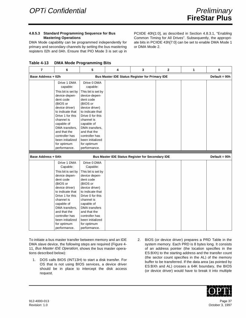
FireStar PlusOPTi Confidential Preliminary
4.8.5.3 Standard Programming Sequence for Bus Mastering Operations
DMA Mode capability can be programmed independently forprimary and secondary channels by setting the bus masteringregisters 02h and 0Ah. Ensure that PIO Mode 3 is set up in
PCIIDE 40h[1:0], as described in Section 4.8.3.1, "EnablingCommon Timing for All Drives". Subsequently, the appropri-ate bits in PCIIDE 43h[7:0] can be set to enable DMA Mode 1or DMA Mode 2.
To initiate a bus master transfer between memory and an IDEDMA slave device, the following steps are required (Figure 4-11, Bus Master IDE Operation, shows the bus master opera-tions described below):
1. DOS calls BIOS (INT13H) to start a disk transfer. ForOS that is not using BIOS services, a device drivershould be in place to intercept the disk accessrequest.
2. BIOS (or device driver) prepares a PRD Table in thesystem memory. Each PRD is 8 bytes long. It consistsof an address pointer (the location specifies in theES:BXh) to the starting address and the transfer count(the sector count specifies in the AL) of the memorybuffer to be transferred. If the data area (as pointed byES:BXh and AL) crosses a 64K boundary, the BIOS(or device driver) would have to break it into multiple
Table 4-13 DMA Mode Programming Bits
7 6 5 4 3 2 1 0
Base Address + 02h Bus Master IDE Status Register for Primary IDE Default = 00h
Drive 1 DMA capable:
This bit is set by device-depen-dent code (BIOS or device driver) to indicate that Drive 1 for this channel is capable of DMA transfers, and that the controller has been initialized for optimum performance.
Drive 0 DMA capable:
This bit is set by device-depen-dent code (BIOS or device driver) to indicate that Drive 0 for this channel is capable of DMA transfers, and that the controller has been initialized for optimum performance.
Base Address + 0Ah Bus Master IDE Status Register for Secondary IDE Default = 00h
Drive 1 DMA Capable:
This bit is set by device depen-dent code (BIOS or device driver) to indicate that Drive 1 for this channel is capable of DMA transfers, and that the controller has been initialized for optimum performance.
Drive 0 DMA Capable:
This bit is set by device depen-dent code (BIOS or device driver) to indicate that Drive 0 for this channel is capable of DMA transfers and that the controller has been initialized for optimum performance.
912-4000-013 Page 37Revision: 1.0 October 3, 1997
OPTi®

FireStar PlusPreliminary OPTi Confidential
transfers (PRDs) so that each of them lies within theboundary.
3. BIOS (or device driver) provides the starting addressof the PRD Table by loading the PRD Table PointerRegister (Bus Master IDE Base Address + 04h or +0Ch).
4. The direction of the data transfer is specified by settingthe Read/write Control bit in the Command Register(Bus Master IDE Base Address + 00h or + 08h). Clearthe Interrupt bit and Error bit in the Status Register(Bus Master IDE Base Address + 02h or + 0Ah).
5. BIOS (device driver) resets the Hard Disk Task Com-plete Flag (a memory byte location at 40:E8h) to 00h.It will be in a tight loop checking whether this CompleteFlag is set to FFh. Other OS may have a differentmechanism to detect disk activity.
6. BIOS (or device driver) specifies address and size ofthe data request by programming the Command BlockRegisters of the IDE device and issues the appropriateDMA transfer command to it.
7. BIOS (device driver) engages the bus master functionby writing ‘1’ to the Start bit in the Command Register(Bus Master IDE Base Address + 00h and + 08h) forthe appropriate channel.
8. The 82C700 starts reading the first PRD and transfersdata to/from its 32-byte FIFO in response to DMArequests (IDEREQx) from the IDE devices. The82C700 then starts transfer to local memory (an inter-nal master request will be generated) for read if theFIFO is empty, for write if the FIFO is full, or when thebyte count expires and no more entries in the PRD.
9. After the last data transfer within a PRD, the 82C700checks the End of Table (EOT) bit to decide whetherto read another PRD or move forward.
10. At the end of transfer, the IDE device signals an inter-rupt.
11. After 82C700 has flushed all the data from its FIFO tosystem memory, it resets the Bus Master IDE Activebit and sets the Interrupt bit in the Status Register.
12. The disk interrupt (DINTx) will be passed to the inter-nal INTC (‘8259). DINTx will not be blocked to theINTC in a disk write operation. This DINTx triggersIRQ14 or IRQ15 and eventually goes to interrupt theCPU.
13. CPU generates an INTA# cycle in responds to theIRQ14 (INT76H) or IRQ15 (INT77H). The INT76Hhandler sets 40:E8h to FFh to signal completion of thedisk access.
14. BIOS (device driver) resets the Start/Stop bit in theCommand Register. It then reads the Status and Inter-
rupt bits in the Status Register and then the IDEdevice’s status to determine if the transfer completedsuccessfully.
15. Status will be passed back to INT13H to finish theoperation.
Page 38 912-4000-013October 3, 1997 Revision: 1.0
OPTi®
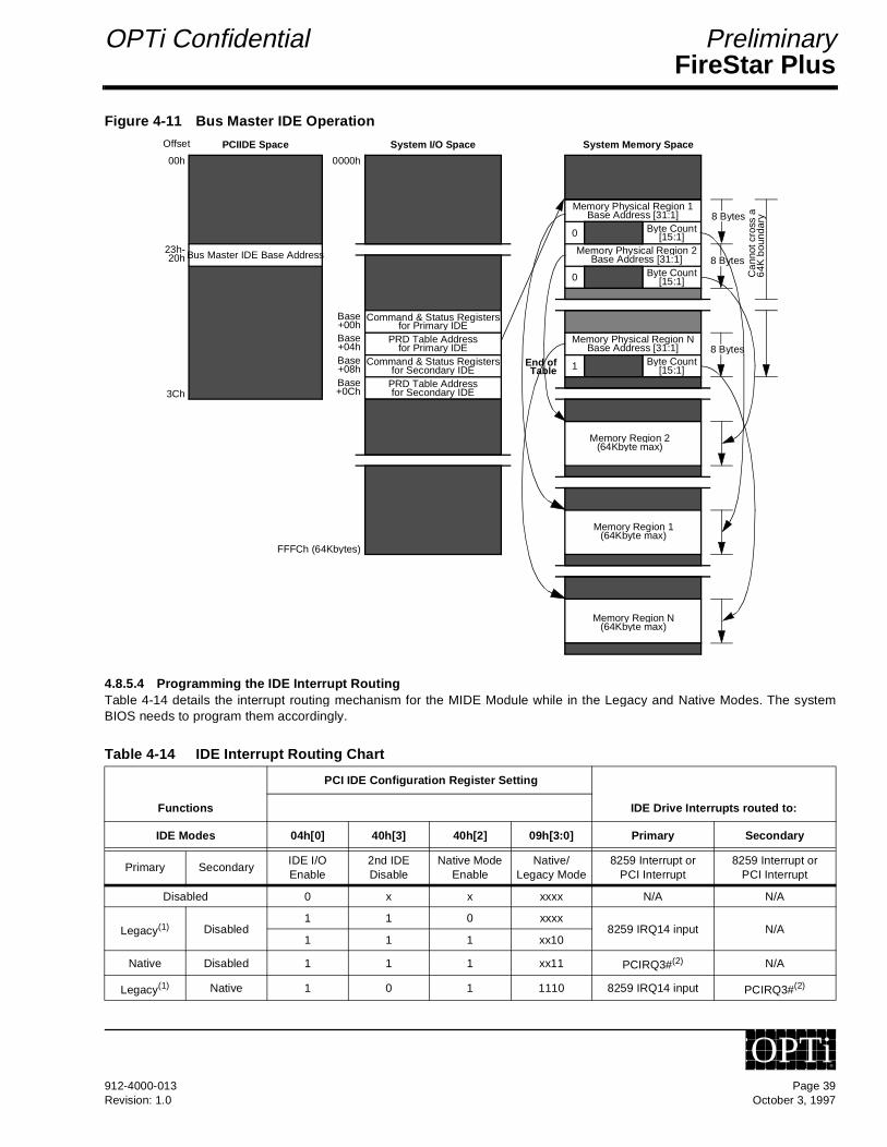
FireStar PlusOPTi Confidential Preliminary
Figure 4-11 Bus Master IDE Operation
4.8.5.4 Programming the IDE Interrupt RoutingTable 4-14 details the interrupt routing mechanism for the MIDE Module while in the Legacy and Native Modes. The systemBIOS needs to program them accordingly.
Table 4-14 IDE Interrupt Routing Chart
Offset
Memory Physical Region 1
Byte Count0
Memory Physical Region 2
Memory Physical Region N
Base Address [31:1]
[15:1]
Base Address [31:1]Byte Count0 [15:1]
Base Address [31:1]Byte Count1 [15:1]
Memory Region 2(64Kbyte max)
Memory Region 1(64Kbyte max)
Memory Region N(64Kbyte max)
Command & Status Registersfor Primary IDE
PRD Table Addressfor Primary IDE
Command & Status Registersfor Secondary IDE
PRD Table Addressfor Secondary IDE
Bus Master IDE Base Address
8 Bytes
00h
23h-20h
3Ch
0000h
Base
Base
Base
Base
FFFCh (64Kbytes)
End ofTable
+00h
+04h
+08h
+0Ch
8 Bytes
8 Bytes
Ca
nnot
cro
ss a
6
4K b
ound
ary
System Memory SpaceSystem I/O SpacePCIIDE Space
Functions
PCI IDE Configuration Register Setting
IDE Drive Interrupts routed to:
IDE Modes 04h[0] 40h[3] 40h[2] 09h[3:0] Primary Secondary
Primary SecondaryIDE I/O Enable
2nd IDE Disable
Native Mode Enable
Native/Legacy Mode
8259 Interrupt or PCI Interrupt
8259 Interrupt or PCI Interrupt
Disabled 0 x x xxxx N/A N/A
Legacy(1) Disabled1 1 0 xxxx
8259 IRQ14 input N/A1 1 1 xx10
Native Disabled 1 1 1 xx11 PCIRQ3#(2) N/A
Legacy(1) Native 1 0 1 1110 8259 IRQ14 input PCIRQ3#(2)
912-4000-013 Page 39Revision: 1.0 October 3, 1997
OPTi®
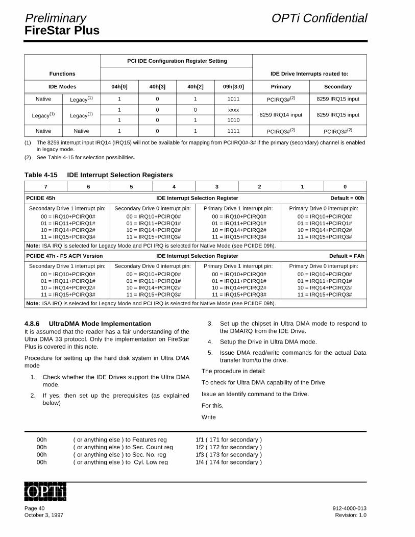
FireStar PlusPreliminary OPTi Confidential
(1) The 8259 interrupt input IRQ14 (IRQ15) will not be available for mapping from PCIIRQ0#-3# if the primary (secondary) channel is enabled in legacy mode.
(2) See Table 4-15 for selection possibilities.
Table 4-15 IDE Interrupt Selection Registers
4.8.6 UltraDMA Mode ImplementationIt is assumed that the reader has a fair understanding of theUltra DMA 33 protocol. Only the implementation on FireStarPlus is covered in this note.
Procedure for setting up the hard disk system in Ultra DMAmode
1. Check whether the IDE Drives support the Ultra DMAmode.
2. If yes, then set up the prerequisites (as explainedbelow)
3. Set up the chipset in Ultra DMA mode to respond tothe DMARQ from the IDE Drive.
4. Setup the Drive in Ultra DMA mode.
5. Issue DMA read/write commands for the actual Datatransfer from/to the drive.
The procedure in detail:
To check for Ultra DMA capability of the Drive
Issue an Identify command to the Drive.
For this,
Write
00h ( or anything else ) to Features reg 1f1 ( 171 for secondary )00h ( or anything else ) to Sec. Count reg 1f2 ( 172 for secondary )00h ( or anything else ) to Sec. No. reg 1f3 ( 173 for secondary )00h ( or anything else ) to Cyl. Low reg 1f4 ( 174 for secondary )
Native Legacy(1) 1 0 1 1011 PCIRQ3#(2) 8259 IRQ15 input
Legacy(1) Legacy(1)1 0 0 xxxx
8259 IRQ14 input 8259 IRQ15 input1 0 1 1010
Native Native 1 0 1 1111 PCIRQ3#(2) PCIRQ3#(2)
7 6 5 4 3 2 1 0
PCIIDE 45h IDE Interrupt Selection Register Default = 00h
Secondary Drive 1 interrupt pin:
00 = IRQ10+PCIRQ0#01 = IRQ11+PCIRQ1#10 = IRQ14+PCIRQ2#11 = IRQ15+PCIRQ3#
Secondary Drive 0 interrupt pin:
00 = IRQ10+PCIRQ0#01 = IRQ11+PCIRQ1#10 = IRQ14+PCIRQ2#11 = IRQ15+PCIRQ3#
Primary Drive 1 interrupt pin:
00 = IRQ10+PCIRQ0#01 = IRQ11+PCIRQ1#10 = IRQ14+PCIRQ2#11 = IRQ15+PCIRQ3#
Primary Drive 0 interrupt pin:
00 = IRQ10+PCIRQ0#01 = IRQ11+PCIRQ1#10 = IRQ14+PCIRQ2#11 = IRQ15+PCIRQ3#
Note: ISA IRQ is selected for Legacy Mode and PCI IRQ is selected for Native Mode (see PCIIDE 09h).
PCIIDE 47h - FS ACPI Version IDE Interrupt Selection Register Default = FAh
Secondary Drive 1 interrupt pin:
00 = IRQ10+PCIRQ0#01 = IRQ11+PCIRQ1#10 = IRQ14+PCIRQ2#11 = IRQ15+PCIRQ3#
Secondary Drive 0 interrupt pin:
00 = IRQ10+PCIRQ0#01 = IRQ11+PCIRQ1#10 = IRQ14+PCIRQ2#11 = IRQ15+PCIRQ3#
Primary Drive 1 interrupt pin:
00 = IRQ10+PCIRQ0#01 = IRQ11+PCIRQ1#10 = IRQ14+PCIRQ2#11 = IRQ15+PCIRQ3#
Primary Drive 0 interrupt pin:
00 = IRQ10+PCIRQ0#01 = IRQ11+PCIRQ1#10 = IRQ14+PCIRQ2#11 = IRQ15+PCIRQ3#
Note: ISA IRQ is selected for Legacy Mode and PCI IRQ is selected for Native Mode (see PCIIDE 09h).
Functions
PCI IDE Configuration Register Setting
IDE Drive Interrupts routed to:
IDE Modes 04h[0] 40h[3] 40h[2] 09h[3:0] Primary Secondary
Page 40 912-4000-013October 3, 1997 Revision: 1.0
OPTi®

FireStar PlusOPTi Confidential Preliminary
00h ( or anything else ) to Cyl High reg 1f5 ( 175 for secondary )A0h to Device/head reg ( for master) 1f6 ( 176 for secondary )
B0h to Device/head reg ( for slave) 1f6 ( 176 for secondary )ECh to Command reg 1f7 ( 177 for secondary )
After the execution of this command, if DRDY in status reg.1F7 ( 177 for secondary ) reads 1, then 255 16 bit words canbe read from the data port 1f0 ( 170 for secondary ). If bit 2 in
word 53 is set, then the device will support Ultra DMA and thevalues reported in word 88 are valid. The definition of thecontents of word 88 are as follows:
Depending on these parameters, the BIOS/Device drivershould enable the appropriate mode of operation.
4.8.6.1 Prerequisites• The system has to be running at 66 Mhz (CPU clock, FS
clock).• For Ultra DMA to work properly, the following features of
the chipset should be enabled. • IDE write concurrency • ISA bus preemption • Arbiter support for PCI/IDE concurrency • Concurrent PCI master IDE and IDE cycle • X-1-1-1 MIDE rd/wr transfers • For this, set PCIIDE Reg. 42 = 56h
Most of these are prerequisites for Disk DMA transfer.
To setup the chipset in Ultra DMA mode for the PrimaryChannel Master Drive (Follow an equivalent process forother drives)
Set PCIIDE 44h bit 0. This enables the Ultra DMA controller.
For setting the mode of transfer, set PCIIDE 44h bits 5 and 4as follows:
00 for mode 0
01 for mode 1
10 for mode 2
These bits control the write timings of the Ultra DMA com-mands.
To setup the Drive in Ultra DMA mode Issue the set featurescommand to the Drive. For this, write
03h to Features reg 1f1 ( 171 for secondary )4xh to Sec. Count reg 1f2 ( 172 for secondary )
x = 0 for mode 01 for mode 12 for mode 2
00h ( or anything else ) to Sec. No. reg 1f3 ( 173 for secondary )00h ( or anything else ) to Cyl. Low reg 1f4 ( 174 for secondary )00h ( or anything else ) to Cyl High reg 1f5 ( 175 for secondary )A0h to Device/head reg ( for master) 1f6 ( 176 for secondary )
B0h to Device/head reg ( for slave) 1f6 ( 176 for secondary )EFh to Command reg 1f7 ( 177 for secondary )
15 14 13 12 11 10 9 8
Reserved Ultra DMA Mode 2 Sta-
tus
0 = Not active1 = Active
Ultra DMA Mode 1 Sta-
tus
0 = Not active1 = Active
Ultra DMA Mode 0 Sta-
tus
0 = Not active1 = Active
7 6 5 4 3 2 1 0
Reserved Ultra DMA-Mode 2 Sup-
port
0 = No
1 = Yes
Ultra DMA-Mode 1 Sup-
port
0 = No
1 = Yes
Ultra DMA-Mode 0 Sup-
port
0 = No
1 = Yes
912-4000-013 Page 41Revision: 1.0 October 3, 1997
OPTi®
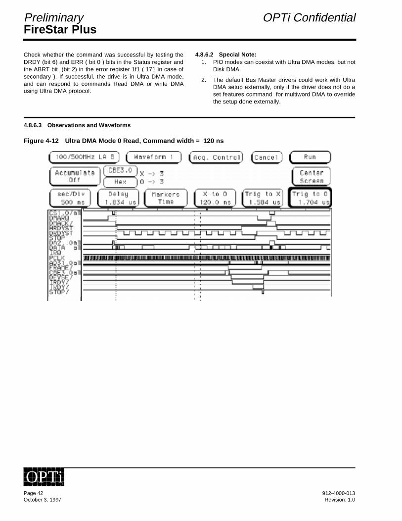
FireStar PlusPreliminary OPTi Confidential
Check whether the command was successful by testing theDRDY (bit 6) and ERR ( bit 0 ) bits in the Status register andthe ABRT bit (bit 2) in the error register 1f1 ( 171 in case ofsecondary ). If successful, the drive is in Ultra DMA mode,and can respond to commands Read DMA or write DMAusing Ultra DMA protocol.
4.8.6.2 Special Note:1. PIO modes can coexist with Ultra DMA modes, but not
Disk DMA.
2. The default Bus Master drivers could work with UltraDMA setup externally, only if the driver does not do aset features command for multiword DMA to overridethe setup done externally.
4.8.6.3 Observations and Waveforms
Figure 4-12 Ultra DMA Mode 0 Read, Command width = 120 ns
Page 42 912-4000-013October 3, 1997 Revision: 1.0
OPTi®

FireStar PlusOPTi Confidential Preliminary
Figure 4-13 Ultra DMA mode 0 write
Figure 4-14 Ultra DMA Mode 1 Read, Command width = 80ns
912-4000-013 Page 43Revision: 1.0 October 3, 1997
OPTi®

FireStar PlusPreliminary OPTi Confidential
Figure 4-15 Ultra DMA mode 1 write
Figure 4-16 Ultra DMA mode 2 read, Command width = 60ns
Page 44 912-4000-013October 3, 1997 Revision: 1.0
OPTi®

FireStar PlusOPTi Confidential Preliminary
Figure 4-17 Ultra DMA mode 2 write
4.8.7 Emulated Bus Mastering ModeFireStar provides a means to have DMA-type operation on aPIO mode drive. Any IDE device can use this feature. Thefeature works by acting as a bus master, in much the sameway as the DMA controller would.
Emulated bus mastering allows devices such as IDE CD-ROM drives to access data and store it in a memory bufferwith no CPU intervention. The interrupt from the IDE drive ishandled by a hardware sequencer; the CPU is interruptedonly after the transfer is complete. The attached IDE drivecan deassert IOCHRDY as needed if data is not ready.
Since the purpose of the Emulated Bus Master IDE mode isprimarily to increase system performance during the diskread from CD-ROM transfer, this mode is implemented forthe read-from-disk direction only.
The differences between PIO mode and DMA mode transferare not only the control signal behavior, but also the program-ming methods to the drive and IDE controller. These aredescribed below. It is important to note that no DMA instruc-tions are allowed to be sent to the drive in this mode, sincethe drive itself is a PIO-mode-only device. No interception ofdrive-related commands takes place, so DMA-related com-mands would only confuse the IDE drive logic.
4.8.7.1 SetupThe IDE controller channel must be programmed to support abus master IDE drive. In addition, the bit corresponding to thechannel must be set in PCIIDE 44h[3:0] for FireStar and PCI-IDE 46h[3:0] for FireStar ACPI to select Emulated Bus Mas-tering (refer to Table 4-16).
4.8.7.2 OperationAs stated earlier, only PIO-mode commands are allowed tothe drive. The emulated bus mastering function automatesonly reads from the drive, so writes must still be carried outthrough normal I/O write cycles from the CPU.
Emulated bus mastering depends on the IRQ line to deter-mine transfer completion. For CD-ROM data read, IRQ isasserted for two reasons:
• When data is ready to be read by host (“data ready IRQ”)
• At the end of the transfer (“transfer complete IRQ”).
This behavior is important to understand for the emulationimplementation.
Data Ready IRQ: When IRQ assertion signals “data ready”,software must act as if it is programming a DMA mode IDEcontroller by doing the following:
• Prepare the required PRD table and word count in memory
• Generate required control commands to the IDE controller. Since the drive used is not DMA-capable, software must not send any DMA commands to the disk drive. Only nor-mal PIO commands can be used.
• Set the Start bit in the IDE controller register.
At this point the hardware takes over and generates the pro-grammed number of I/O read cycles to the CD-ROM drive.During the transfer, the IDE controller uses the existing busmaster IDE control state machine and logic to perform theoperation. The signal DCS1# is forced active, DCS3# isforced inactive, and DDACK# is masked, before being sent to
912-4000-013 Page 45Revision: 1.0 October 3, 1997
OPTi®
FireStar PlusPreliminary OPTi Confidential
the disk drive interface. Therefore, the CD-ROM is seeingPIO mode data read transfer control.
Transfer Complete IRQ: When the word count expires in theIDE controller and CD-ROM drive, IRQ is asserted to signal“transfer completed”. Software must:
• Reset the Start bit in the IDE controller register
• Read the controller status and then the drive status to determine whether the transfer completed successfully.
Table 4-16 Emulated Bus Master Control Registers
7 6 5 4 3 2 1 0
PCIIDE 44h Emulated Bus Master Register Default = 00h
Reserved Emulated bus mastering for
Cable 1, Drive 1:
0 = Disable1 = Enable
Emulated bus mastering for
Cable 1, Drive 0:
0 = Disable1 = Enable
Emulated bus mastering for
Cable 0, Drive 1:
0 = Disable1 = Enable
Emulated bus mastering for
Cable 0, Drive 0:
0 = Disable1 = Enable
PCIIDE 46h - FS ACPI Version Emulated IDE Configuration Register Default = 00h
Fix for I/O 32-bit Mode 4 and
Mode 5 timing:
0 = Disable1 = Enable
Reserved Emulated bus mastering for
Cable 1, Drive 1:
0 = Disable1 = Enable
Emulated bus mastering for
Cable 1, Drive 0:
0 = Disable1 = Enable
Emulated bus mastering for
Cable 0, Drive 1:
0 = Disable1 = Enable
Emulated bus mastering for
Cable 0, Drive 0:
0 = Disable1 = Enable
Page 46 912-4000-013October 3, 1997 Revision: 1.0
OPTi®
FireStar PlusOPTi Confidential Preliminary
5.0 PIR Table for FireStar PlusThis section describes the OPTi-recommended means ofsupporting the Microsoft IRQ miniport function for FireStar.Microsoft has already incorporated this support into Memphisstarting from build 15xxyy. All future Memphis versions willtherefore incorporate support according to the scheme pre-sented below. The IRQ miniport drivers for OSR2 are avail-able as a QFE on the OPTi website.
5.1 OverviewIn the Microsoft-defined $PIR table, there is an entry for eachslot that is organized as shown below. The Link value isOEM-specific. The complete table format can be found on theMicrosoft webwite (file name PCIIRQ.HTM).
Because OPTi chipsets are so flexible as regards PCI inter-rupt possibilities, there are unlimited combinations that couldbe used in any system. However, a single Miniport drivermust be able to route interrupts for all cases.
OPTi is proposing a common scheme for all BIOS vendors touse for this Link value that will allow Microsoft Windows andother OSes to perform dynamic IRQ routing for PCI devicesregardless of how the system has been designed.
5.2 OPTi PCI Interrupt Source OverviewThere are four sources of PCI interrupts in an OPTi-basedsystem.
• ISA IRQs converted to PCI interrupts - FireStar has eight ISA interrupt pins, IRQA, B, C, D, E, F, G, and H, each of which can be mapped to any IRQ line. The conversion to PCI-type interrupt is very simple: there is an edge/level bit in the IRQ routing register for each pin. The routing regis-ters are located at PCIDV1 B0h-B7h.
• PIO pins programmed as PCIRQ# pins - FireStar has 32 PIO pins, any of which can be programmed to become PCIRQ0#, PCIRQ1#, PCIRQ2#, or PCIRQ3#. Once the assignment has been made (by BIOS), the routing of each PCIRQ# pin to an ISA IRQ is controlled by writing a corre-sponding 4-bit value in PCIDV1 B8h-B9h.
• Docking Station PCIRQ# pins - An OPTi system using an OPTi 82C814 FireBridge Docking Controller (or 82C824 FireFox CardBus Controller in docking mode) also has PCIRQ0#, PCIRQ1#, PCIRQ2#, and PCIRQ3# pins. Once enabled, through PCICFG 48h-4Bh of the 82C814 PCI configuration registers (default is direct-map enabled), their mapping to ISA IRQs is controlled by PCIDV1 B8h-B9h (same as for the PIO pins). Mapping can be 'twisted' if desired for more even interrupt sharing.
• Serial IRQ pin - OPTi systems support the Compaq single-wire IRQSER line. Once serial IRQs are enabled (by BIOS), the PCIRQ# mapping to ISA IRQs is controlled by PCIDV1 B8h-B9h (same as for the PIO pins).
The regular means in which these interrupt controls havebeen implemented makes it straightforward to implement aunified interrupt router.
5.3 OPTi-Suggested Link Value SchemeThis suggested layout should cover all cases of interruptassignment both on docking stations and on local devices, nomatter what configuration is selected.
5.3.1 Proposed Usa ge
a. If bits [2:0]=00, entire link byte must be set to zero to indicate "no connection."
Byte Off set Name
0 PCI Bus Number
1 PCI Device Number (in upper 5 bits)
2 Link value for INTA#
3-4 IRQ bitmap for INTA#
5 Link value for INTB#
6-7 IRQ bitmap for INTB#
8 Link value for INTC#
9-10 IRQ bitmap for INTC#
11 Link value for INTD#
12-13 IRQ bitmap for INTD#
14 Slot Number
15 Reserved
Name 7 6 5 4 3 2 1 0
$PIR Link Value
Reserved, Write as 0
Register Offset in IRQ Selection Source (REGOFST) - This value is used to compute the location of the PCI Configuration Register used to set this interrupt.
Reserved, Write as 0
IRQ Selection Source
000=No interrupt connectiona
001=FireStar IRQ pin
010=FireStar PIO pin or Serial IRQ PIRQ#
011=FireBridge 1 INTx# pin
1xx=reserved
912-4000-013 Page 47Revision: 1.0 October 3, 1997
OPTi®
FireStar PlusPreliminary OPTi Confidential
5.3.2 IRQ Selection Source and Register OffsetThese values indicate how the routing registers can beaccessed. It works like this.
01=FireStar IRQ pin - There are eight ISA IRQ lines that canbe used in the system design as PCI interrupts. These areaccessed through PCIDV1 B0-B7h of the FireStar PCI config-uration registers, which all have the following format.
Select the desired IRQ mapping by writing its value toPCIDV1 (B0h+REGOFST) bits [0:3], and set bit [4]=1 toselect PCI level mode. Avoid changing the value of bit [7],which is design-dependent.
10=FireStar PIO pin or Serial IRQ PIRQ# - There are 32PIO lines that can be preconfigured by BIOS as PCI PCIRQ0-
3#. Also, if Serial IRQs are used, they can provide equivalentPCIRQ# inputs. In both cases, the PCIRQ0-3# lines areinternally routed to ISA interrupts through PCIDV1 B8-B9h ofthe FireStar PCI configuration registers, which have the fol-lowing format.
Select the desired IRQ mapping by writing its value as a nib-ble to the 16-bit value at PCIDV1 B8h, shifted left by thevalue in REGOFST times 4 bits. So if the link value connectsthe slot INTA# to the PIO PCIRQ2# input, its REGOFSTvalue should be 02h (shift the nibble left by two nibbles, 8bits, within the word at B8h).
Note that a restriction on the first FireStar production siliconinhibits sharing the same interrupt through a redirected ISAIRQ line with one coming into a PIO pin PCIRQ# line. Forexample, assigning PCIRQ3# as IRQ7 automatically blocksthe IRQ coming from the IRQ7 pin, regardless of whether itwas programmed as a PCI interrupt or not. This restriction
has been removed starting from FireStar ACPI production(please contact OPTi for details if needed).
However, interrupts from PIO pins and from the serial IRQinput are always sharable, on all silicon revisions.
11=FireBridge 1 INTx pin - On any OPTi docking stationlevel, there are four PCI interrupt lines INTA#-INTD# that canbe mapped, just like the PIO pins mentioned above, to thePIO PCIRQ0-3# inputs. So when a PCI device is detected onany non zero PCI bus, the same mechanism mentionedabove applies.
For further flexibility, the INTA#-INTD# mapping to PCIRQ0#-PCIRQ3# can be switched at the source. PCICFG 48-4Bh
Name 7 6 5 4 3 2 1 0
IRQx Intr. Select Reg.
Pulldown set-ting - please do not alter this bit
Reserved - please do not alter these bits
Interrupt Type
0 = ISA
1 = PCI
Interrupt Selection on this pin
0000=Disabled
0001=IRQ1 0110=IRQ6 1011=IRQ11
0010=rsvd 0111=IRQ7 1100=IRQ12
0011=IRQ3 1000=IRQ8# 1101=rsvd
0100=IRQ4 1001=IRQ9 1110=IRQ14
0101=IRQ5 1010=IRQ10 1111=IRQ15
PCI DV1 Name 7 6 5 4 3 2 1 0
B8h PCI Inter-rupt Selec-tion Register 1
Interrupt Selection on PIO PCIRQ1# input
0000=Disabled
0001=IRQ1 0110=IRQ6 1011=IRQ11
0010=rsvd 0111=IRQ7 1100=IRQ12
0011=IRQ3 1000=IRQ8# 1101=rsvd
0100=IRQ4 1001=IRQ9 1110=IRQ14
0101=IRQ5 1010=IRQ10 1111=IRQ15
Interrupt Selection on PIO PCIRQ0# input
0000=Disabled
0001=IRQ1 0110=IRQ6 1011=IRQ11
0010=rsvd 0111=IRQ7 1100=IRQ12
0011=IRQ3 1000=IRQ8# 1101=rsvd
0100=IRQ4 1001=IRQ9 1110=IRQ14
0101=IRQ5 1010=IRQ10 1111=IRQ15
B9h PCI Inter-rupt Selec-tion Register 2
Interrupt Selection on PIO PCIRQ3# input
0000=Disabled
0001=IRQ1 0110=IRQ6 1011=IRQ11
0010=rsvd 0111=IRQ7 1100=IRQ12
0011=IRQ3 1000=IRQ8# 1101=rsvd
0100=IRQ4 1001=IRQ9 1110=IRQ14
0101=IRQ5 1010=IRQ10 1111=IRQ15
Interrupt Selection on PIO PCIRQ2# input
0000=Disabled
0001=IRQ1 0110=IRQ6 1011=IRQ11
0010=rsvd 0111=IRQ7 1100=IRQ12
0011=IRQ3 1000=IRQ8# 1101=rsvd
0100=IRQ4 1001=IRQ9 1110=IRQ14
0101=IRQ5 1010=IRQ10 1111=IRQ15
Page 48 912-4000-013October 3, 1997 Revision: 1.0
OPTi®
FireStar PlusOPTi Confidential Preliminary
correspond to the INTA#-INTD# inputs on the secondary sideof the bridge. Registers 48h-4Bh default to 01-02-03-04 for adirect mapping, but can be rewritten if desired to change themapping structure. Refer to the 82C814 FireBridge 1 databook for details.
5.3.3 Example of a PCI IRQ routing table: Given below is an example of a PCI IRQ routing table on anOPTi FireStar evaluation board.
The remaining "slot" link values are given below:
Byte OffsetSize in bytes Value Description
0 4 52h,49h,59h,24h This is the signature $PIR for this table
4 2 01h, 00h This indicates the major version to be 1 and the minor version to be 0
6 2 00h, 90h This indicates the table size in a hexadecimal value
8 1 00h The bus number of the PCI interrupt router
9 1 08h The device number and function number of the PCI interrupt router. The upper 5 bits indicate the device number and the lower 3 bits indicate the function number
10 2 00h, 00h No IRQs are devoted exclusively to PCI
12 4 00h, 00h, 00h, 00h
This value indicates that there is no compatible PCI interrupt router that uses the same method for mapping PIRQ# links to IRQs
16 4 00h, 00h, 00h, 00h
No additional information is required for the IRQ miniport driver
20 11 00h Reserved (set to zero)
31 1 71h checksum - such that the sum of all the entries in the $PIR table, including the checksum value, modulo 256, is zero
32 1 00h PCI bus number for 1st "slot"
33 1 28h Device number of this "slot" - in the upper 5 bits
34 1 51h Link Value for INTA# - refer to previous explanation of the OPTi Link value encoding scheme
35 2 9Eh, F8h IRQ bitmap for INTA#. This particular value tells you that you cannot map this PCIIRQ to IRQ14, IRQ13, IRQ8, IRQ2, IRQ1, and IRQ0
37 1 61h Link Value for INTB#
38 2 9Eh, F8h IRQ bitmap for INTB#
40 1 71h Link Value for INTC#
41 2 9Eh, F8h IRQ bitmap for INTC#
43 1 32h Link Value for INTD#
44 2 9Eh, F8h IRQ bitmap for INTD#
46 1 01h Slot number
47 1 00h Reserved
Continued Below
PCI bus# Device# LA
IRQ map for
INTA LBIRQ map for INTB LC
IRQ map for INTC LD
IRQ map for INTD Slot # Rsvd
00 06 61 9ef8 71 9ef8 32 9ef8 51 9ef8 02 00
00 07 71 9ef8 32 9ef8 51 9ef8 61 9ef8 03 00
00 04 02 9ef8 12 9ef8 22 9ef8 32 9ef8 00 00
912-4000-013 Page 49Revision: 1.0 October 3, 1997
OPTi®
FireStar PlusPreliminary OPTi Confidential
LA = Link Value for INTA#
LB = Link Value for INTB#
LC = Link Value for INTC#
LD = Link Value for INTD#
Figure 5-1 PCI Interrupts Mapping Matrix
01 00 02 9ef8 12 9ef8 22 9ef8 32 9ef8 04 00
01 01 12 9ef8 22 9ef8 32 9ef8 02 9ef8 05 00
01 02 22 9ef8 32 9ef8 02 9ef8 12 9ef8 06 00
PCI bus# Device# LA
IRQ map for
INTA LBIRQ map for INTB LC
IRQ map for INTC LD
IRQ map for INTD Slot # Rsvd
IRQF
IRQG
IRQH
PIOx
INTA#
INTB#
INTC#
INTD#
Dev-5 Dev-6 Dev-7
PCIRQ0#
PCIRQ1#
PCIRQ2#
PCIRQ3#
Dev-0 Dev-1 Dev-2
82C814FireStar Plus
PCI Bus 0 PCI Bus 1
Linked through IRQ Driveback(no physical connection to INTx# pins)
Dev-4
Page 50 912-4000-013October 3, 1997 Revision: 1.0
OPTi®
FireStar PlusOPTi Confidential Preliminary
6.0 Interfacing t he FireStar Plus Chipset wi th the 82C602AThe aim of this section is to illustrate how the FireStar Pluschipset can be interfaced with the 82C602A. The connectivityillustrated in this document is one of the ways that the82C602A can be interfaced to the FireStar Plus chipset.
6.1 Purpose of Using the 82C602ABy utilizing the 82C602A companion chip in it's Viper Note-book Mode A configuration, one gains the following (asopposed to a non 82C602A, FireStar chipset based system):
• 8 power management inputs are now available, muxed in with the DRQs and IRQ8# on the four EPMMUX pins.
• 7 full-featured PIO pins are available on the original DRQ0-7 pins and IRQ8# pin of FireStar.The number of pins is actually 8, but is reduced by 1 because one must be programmed as ATCLK/2.
• 12 PPWR outputs are generated by latching the SD bus lines from PCTLH (FireStar PPWRL) and PCTLL (FireStar RSTDRV).
• An internal RTC. This precludes the need for an external RTC.
The ISA bus RSTDRV signal is now generated by the82C602A chip, so that the FireStar RSTDRV pin can be usedfor PPWR generation (power control latch control signal). Ifthe extra PPWR signals are not needed, the FireStar RST-DRV pin becomes useful as a full-featured PIO pin.
6.2 Connectivi tyThe actual connectivity of the 82C602A is shown on theattached Orcad schematic page. This connectivity isdescribed below.
6.2.1 Strapping t he 82C602AThe 82C602A needs to be used in the Viper Notebook ModeA (VNBA). To strap the 82C602A into the VNBA mode, theXD4 and XD0 signals on the 82C602A must be connected toGND via a 4.7K pulldown resistor. The rest of the XD linesneed to be pulled up to +5V (10K resistors).
6.2.2 Using the 82C602A Inter nal RTCThe IRQ8# pin (Pin 56) of the 82C602A is pulled up (to 5V or3.3V) and not connected anywhere else. The IRQ8# is sentout on the EPMMUX1 output of the 82C602A to the FireStarchipset.
The XD[7:0] bus from FireStar is connected to the SD[7:0] ofthe 82C602A. The XDIR pin (pin 72) of the 82C602A shouldbe pulled upto 5V.
6.2.3 DREQ# and DACK# Co nnectivityThe DACK#[2:0] pins from FireStar are configured asEDACK[2:0] outputs, and the rest of the DACK# lines havebeen configured as EPMMUX[3:0] inputs. The new DACK#utilization has been tabulated below.
Table 6-1 DACK# Encodi ng
Table 6-2 New DACK# Util ization
Original Name New Signal Decoder Input Decoder Output
DACK0# (O) EDACK0 (O) A DACK0-7# correspond to decoder outputs Y0-Y7
DACK1# (O) EDACK1 (O) B
DACK2# (O) EDACK2 (O) C
Orig inal Name New Signal Mux Input ATCLK/2 (B) ATCLK (A) Muxed Signals
DACK3# (O) EPMMUX0 (I) C0 0 0 RINGI
C1 0 1 EPMI2#
C2 1 0 EPMI3#
C3 1 1 LLOBAT
DACK5# (O) EPMMUX1 (I) C0 0 0 IRQ8#
C1 0 1 EPMI0#
C2 1 0 EPMI1#
C3 1 1 LOBAT
912-4000-013 Page 51Revision: 1.0 October 3, 1997
OPTi®
FireStar PlusPreliminary OPTi Confidential
The DRQ[7:5, 3:0] pins on FireStar have been configured asPIO pins. DRQ[7:5, 3:0] from ISA devices are brought into the82C602A and sent to FireStar on the EPMMUX[3:2] lines.
To enable the muxing of these signals within the 82C602A,the ATCLK and ATCLK2 signals from FireStar are connectedto the 82C602A. ATCLK2 must be programmed to come outon a FireStar PIO pin.
6.2.4 Miscellaneous Power management connectivity
To increase the number of PPWR pins available for Powermanagement (powering down individual power planes on thesystem, powering down components, enabling/disabling sus-pend mode of operation for various system components,etc.), the SD lines from FireStar have been connected to theSA[5:0] lines and HDCHRDY line of the 82C602A. These sig-nals are inputs to two internal latches and the latched out-puts are the corresponding PPWR outputs. The PPWR0 andthe RSDTRV outputs from FireStar are configured as theupper and lower latch enables respectively and are con-nected to the PCTLH (pin 51) and the PCTLL (pin 87) of the82C602A.
Miscellaneous power management inputs are brought intothe 82C602A (on the RINGI, EPMI#0, etc., inputs) and aresent to FireStar as muxed outputs on the EPMMUX[1:0]lines.
DACK6# (O) EPMMUX2 (I) C0 0 0 DRQ0
C1 0 1 DRQ1
C2 1 0 DRQ2
C3 1 1 DRQ3
DACK7# (O) EPMMUX3 (I) C0 0 0 PWRBTN#
C1 0 1 DRQ5
C2 1 0 DRQ6
C3 1 1 DRQ7
Original Name New Signal Mux Input ATCLK/2 (B) ATCLK (A) Muxed Signals
Page 52 912-4000-013October 3, 1997 Revision: 1.0
OPTi®
FireStar PlusOPTi Confidential Preliminary
Figure 6-1 Schematics with 602A
912-4000-013 Page 53Revision: 1.0 October 3, 1997
OPTi®

FireStar PlusPreliminary OPTi Confidential
Page 54 912-4000-013October 3, 1997 Revision: 1.0
OPTi®
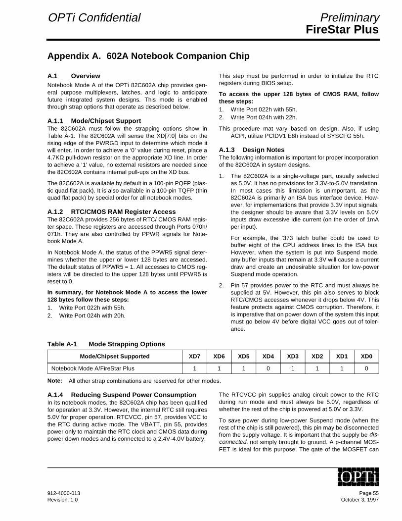
FireStar PlusOPTi Confidential Preliminary
Appendix A. 602A Notebook Companion Chip
A.1 OverviewNotebook Mode A of the OPTi 82C602A chip provides gen-eral purpose multiplexers, latches, and logic to anticipatefuture integrated system designs. This mode is enabledthrough strap options that operate as described below.
A.1.1 Mode/Chipset SupportThe 82C602A must follow the strapping options show inTable A-1. The 82C602A will sense the XD[7:0] bits on therising edge of the PWRGD input to determine which mode itwill enter. In order to achieve a ‘0’ value during reset, place a4.7KΩ pull-down resistor on the appropriate XD line. In orderto achieve a ‘1’ value, no external resistors are needed sincethe 82C602A contains internal pull-ups on the XD bus.
The 82C602A is available by default in a 100-pin PQFP (plas-tic quad flat pack). It is also available in a 100-pin TQFP (thinquad flat pack) by special order for all notebook modes.
A.1.2 RTC/CMOS RAM Register AccessThe 82C602A provides 256 bytes of RTC/ CMOS RAM regis-ter space. These registers are accessed through Ports 070h/071h. They are also controlled by PPWR signals for Note-book Mode A.
In Notebook Mode A, the status of the PPWR5 signal deter-mines whether the upper or lower 128 bytes are accessed.The default status of PPWR5 = 1. All accesses to CMOS reg-isters will be directed to the upper 128 bytes until PPWR5 isreset to 0.
In summary, for Notebook Mode A to access the lower128 bytes follow these steps:1. Write Port 022h with 55h.2. Write Port 024h with 20h.
This step must be performed in order to initialize the RTCregisters during BIOS setup.
To access the upper 128 bytes of CMOS RAM, followthese steps:1. Write Port 022h with 55h.2. Write Port 024h with 22h.
This procedure mat vary based on design. Also, if usingACPI, utilize PCIDV1 E8h instead of SYSCFG 55h.
A.1.3 Design NotesThe following information is important for proper incorporationof the 82C602A in system designs.
1. The 82C602A is a single-voltage part, usually selectedas 5.0V. It has no provisions for 3.3V-to-5.0V translation.In most cases this limitation is unimportant, as the82C602A is primarily an ISA bus interface device. How-ever, for implementations that provide 3.3V input signals,the designer should be aware that 3.3V levels on 5.0Vinputs draw excessive idle current (on the order of 1mAper input).
For example, the ‘373 latch buffer could be used tobuffer eight of the CPU address lines to the ISA bus.However, when the system is put into Suspend mode,any buffer inputs that remain at 3.3V will cause a currentdraw and create an undesirable situation for low-powerSuspend mode operation.
2. Pin 57 provides power to the RTC and must always besupplied at 5V. However, this pin also serves to blockRTC/CMOS accesses whenever it drops below 4V. Thisfeature protects against CMOS corruption. Therefore, itis imperative that on power down of the system this inputmust go below 4V before digital VCC goes out of toler-ance.
Table A-1 Mode Strapping Options
Note: All other strap combinations are reserved for other modes.
A.1.4 Reducing Suspend Power ConsumptionIn its notebook modes, the 82C602A chip has been qualifiedfor operation at 3.3V. However, the internal RTC still requires5.0V for proper operation. RTCVCC, pin 57, provides VCC tothe RTC during active mode. The VBATT, pin 55, providespower only to maintain the RTC clock and CMOS data duringpower down modes and is connected to a 2.4V-4.0V battery.
The RTCVCC pin supplies analog circuit power to the RTCduring run mode and must always be 5.0V, regardless ofwhether the rest of the chip is powered at 5.0V or 3.3V.
To save power during low-power Suspend mode (when therest of the chip is still powered), this pin may be disconnectedfrom the supply voltage. It is important that the supply be dis-connected, not simply brought to ground. A p-channel MOS-FET is ideal for this purpose. The gate of the MOSFET can
Mode/Chipset Supported XD7 XD6 XD5 XD4 XD3 XD2 XD1 XD0
Notebook Mode A/FireStar Plus 1 1 1 0 1 1 1 0
912-4000-013 Page 55Revision: 1.0 October 3, 1997
OPTi®
FireStar PlusPreliminary OPTi Confidential
be controlled by PPWR0 or PPWR1 from the power controllatch.
For example, PPWR0 may be used to switch off RTCVCC byusing a P-channel MOSFET as shown in Figure A-1. Theauto-toggle feature of the PPWR0 line must be enabled,54h[0] = 0, and 68h[0] = 1. Setting bits 68h[3:2] = 10 providesthe necessary recovery time to the RTC analog VCC. Withthis implementation, the MOSFET will switch off the power ofthe analog VCC only during Suspend mode; the only currentflow through the analog VCC is leakage current (less than1µA).
Figure A-1 RTCVCC Switching Circuit Example
The MOSFET used for testing at OPTi is a National Semicon-ductor NDF0610, which has a typical gate threshold voltageof -2.4V (-3.5V max / -1V min).
A.1.5 Power Consumption MeasurementsUsing the circuit of Figure A-1, the power consumption of the82C602A Notebook Mode in use with the OPTi FireStar Pluschip demonstration board is shown in the following twotables.
Table A-2 Typical Current Consumption Figures for RTC Power
Table A-3 Typical Current Consumption Figures for Digital Power
A.1.6 Internal Real-Time Clock (RTC)The internal RTC of the 82C602A is functionally compatiblewith the Benchmarq BQ3285. The following sub-sections willgive detailed functional and register features of the on-chipRTC of the 82C602A.
RTC Features• System wake-up capability -- alarm interrupt output active
in battery back-up mode
• 4.5V to 5.5V operation
• 242 bytes of general non-volatile storage
• Direct clock/calendar replacement for IBM® AT-compatible computers and other applications
• Less than 1.0µA load under battery operation
• 14 bytes for clock/calendar and control
• BCD or binary format for clock and calendar data
• Calendar in day of the week, day of the month, months, and years, with automatic leap-year adjustment
• Time of day in seconds, minutes, and hours- 12- or 24-hour format- Optional daylight saving adjustment
• Three individually maskable interrupt event flags:- Periodic rates from 122µs to 500ms- Time-of-day alarm once-per-second to-once-per-day- End-of-clock update cycle.
RTC OverviewThe on-chip RTC is a low-power microprocessor peripheralproviding a time-of-day clock and 100 year calendar withalarm features and battery operation. The RTC supports 3.3Vsystems. Other RTC features include three maskable inter-rupt sources, square-wave output, and 242 bytes of generalnon-volatile storage.
Wake-up capability is provided by an alarm interrupt, which isactive in battery back-up mode.
The RTC write-protects the clock, calendar, and storage reg-isters during power failure. A back-up battery then maintainsdata and operates the clock and calendar.
The on-chip RTC is a fully compatible real-time clock for PC/AT-compatible computers and other applications. The onlyexternal components are a 32.768kHz crystal and a back-upbattery.
RTC Address MapThe on-chip RTC provides 14 bytes of clock and control/sta-tus registers and 242 bytes of general non-volatile storage.Figure A-2 illustrates the address map for the RTC.
Parameter Normal Suspend
Analog VCC < 1.5µA ~1µA
VBAT ~1µA ~1µA
Digital VCC = 3.3V Digital VCC = 5.0V
Normal Suspend Normal Suspend
< 4mA < 30µA < 4mA 250µA
PPWR0
5.0V
1441497191
57
82C602A
3.3V or 5.0V
NDF0610P-ChannelMOSFET
VCC
RTCVCC
Page 56 912-4000-013October 3, 1997 Revision: 1.0
OPTi®
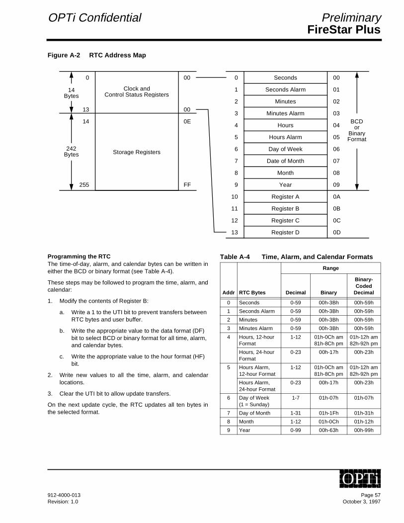
FireStar PlusOPTi Confidential Preliminary
Figure A-2 RTC Address Map
Programming the RTCThe time-of-day, alarm, and calendar bytes can be written ineither the BCD or binary format (see Table A-4).
These steps may be followed to program the time, alarm, andcalendar:
1. Modify the contents of Register B:
a. Write a 1 to the UTI bit to prevent transfers between RTC bytes and user buffer.
b. Write the appropriate value to the data format (DF) bit to select BCD or binary format for all time, alarm, and calendar bytes.
c. Write the appropriate value to the hour format (HF) bit.
2. Write new values to all the time, alarm, and calendarlocations.
3. Clear the UTI bit to allow update transfers.
On the next update cycle, the RTC updates all ten bytes inthe selected format.
Table A-4 Time, Alarm, and Calendar Formats
Seconds
Seconds Alarm
Minutes
Minutes Alarm
Hours
Hours Alarm
Day of Week
Date of Month
Month
Year
Register A
Register B
Register C
Register D
0
1
2
3
4
5
6
7
8
9
10
11
12
13
00
01
02
03
04
05
06
07
08
09
0A
0B
0C
0D
BCDor
BinaryFormat
Clock and
Storage Registers
0
13
14
255
00
00
0E
FF
Control Status Registers14
Bytes
242Bytes
Addr RTC Bytes
Range
Decimal Binary
Binary-Coded
Decimal
0 Seconds 0-59 00h-3Bh 00h-59h
1 Seconds Alarm 0-59 00h-3Bh 00h-59h
2 Minutes 0-59 00h-3Bh 00h-59h
3 Minutes Alarm 0-59 00h-3Bh 00h-59h
4 Hours, 12-hour Format
1-12 01h-0Ch am81h-8Ch pm
01h-12h am82h-92h pm
Hours, 24-hour Format
0-23 00h-17h 00h-23h
5 Hours Alarm, 12-hour Format
1-12 01h-0Ch am81h-8Ch pm
01h-12h am82h-92h pm
Hours Alarm, 24-hour Format
0-23 00h-17h 00h-23h
6 Day of Week (1 = Sunday)
1-7 01h-07h 01h-07h
7 Day of Month 1-31 01h-1Fh 01h-31h
8 Month 1-12 01h-0Ch 01h-12h
9 Year 0-99 00h-63h 00h-99h
912-4000-013 Page 57Revision: 1.0 October 3, 1997
OPTi®

FireStar PlusPreliminary OPTi Confidential
Square-wave OutputThe RTC divides the 32.768kHz oscillator frequency to pro-duce the 1Hz update frequency for the clock and calendar.Thirteen taps from the frequency divider are fed to a 16:1multiplexer circuit. The output of this mux is fed to the SQWoutput and periodic interrupt generation circuitry. The fourleast-significant bits of Register A, RS[3:0], select among the13 taps (see Table A-5).
InterruptsThe RTC allows three individually selected interrupt events togenerate an interrupt request. These three interrupt eventsare:
1. The periodic interrupt, programmable to occur onceevery 122µs to 500ms.
2. The alarm interrupt, programmable to occur once-per-second to once-per-day, is active in battery back-upmode, providing a “wake-up” feature.
3. The update-ended interrupt, which occurs at the end ofeach update cycle.
Each of the three interrupt events is enabled by an individualinterrupt enable bit in Register B. When an event occurs, its
event flag bit in Register C is set. If the corresponding eventenable bit is also set, then an interrupt request is generated.The interrupt request flag bit (INTF) of Register C is set withevery interrupt request. Reading Register C clears all flagbits, including INTF, and makes INT# high-impedance.
Two methods can be used to process RTC interrupt events:
1. Enable interrupt events and use the interrupt requestoutput to invoke an interrupt service routine.
2. Do not enable the interrupts and use a polling routine toperiodically check the status of the flag bits.
The individual interrupt sources are described in detail in thefollowing sub-sections.
Periodic InterruptThe mux output used to drive the SQW output also drives theinterrupt generation circuitry. If the periodic interrupt event isenabled by writing a 1 to the periodic interrupt enable bit(PIE) in Register C, an interrupt request is generated onceevery 122µs to 500ms. The period between interrupts isselected by the same bits in Register A that select thesquare-wave frequency (see Table A-5). Setting OSC[2:0] inRegister A to 011 does not affect the periodic interrupt timing.
Table A-5 Square-Wave Frequency/Periodic Interrupt Rate
Alarm InterruptThe alarm interrupt is active in battery back-up mode, provid-ing a “wake-up” capability. During each update cycle, theRTC compares the hours, minutes, and seconds bytes withthe three corresponding alarm bytes. If a match of all bytes is
found, the alarm interrupt event flag bit, AF in Register C, isset to 1. If the alarm event is enabled, an interrupt request isgenerated.
Register A Bits Square-Wave Periodic Interrupt
RS3 RS2 RS1 RS0 Frequency Units Period Units
0 0 0 0 None None
0 0 0 1 256 Hz 3.90625 ms
0 0 1 0 128 Hz 7.8125 ms
0 0 1 1 8.192 kHz 122.070 µs
0 1 0 0 4.096 kHz 244.141 µs
0 1 0 1 2.048 kHz 488.281 µs
0 1 1 0 1.024 kHz 976.5625 µs
0 1 1 1 512 Hz 1.953125 ms
1 0 0 0 256 Hz 3.90625 ms
1 0 0 1 128 Hz 7.8125 ms
1 0 1 0 64 Hz 15.625 ms
1 0 1 1 32 Hz 31.25 ms
1 1 0 0 16 Hz 62.5 ms
1 1 0 1 8 Hz 125 ms
1 1 1 0 4 Hz 250 ms
1 1 1 1 2 Hz 500 ms
Page 58 912-4000-013October 3, 1997 Revision: 1.0
OPTi®
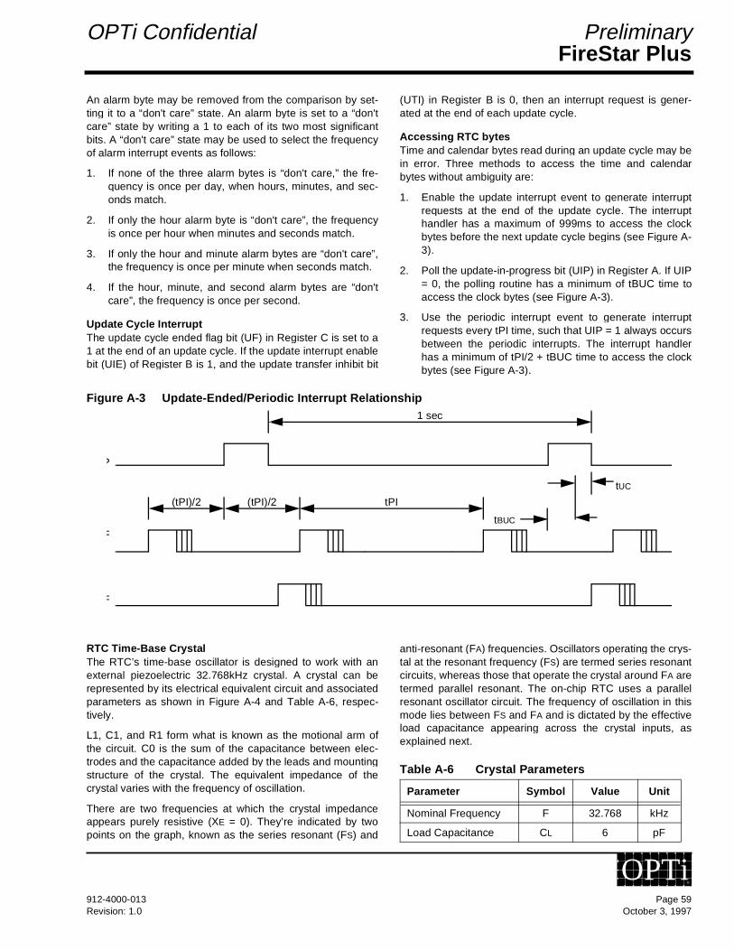
FireStar PlusOPTi Confidential Preliminary
An alarm byte may be removed from the comparison by set-ting it to a “don't care” state. An alarm byte is set to a “don'tcare” state by writing a 1 to each of its two most significantbits. A “don't care” state may be used to select the frequencyof alarm interrupt events as follows:
1. If none of the three alarm bytes is “don't care,” the fre-quency is once per day, when hours, minutes, and sec-onds match.
2. If only the hour alarm byte is “don't care”, the frequencyis once per hour when minutes and seconds match.
3. If only the hour and minute alarm bytes are “don't care”,the frequency is once per minute when seconds match.
4. If the hour, minute, and second alarm bytes are “don'tcare”, the frequency is once per second.
Update Cycle InterruptThe update cycle ended flag bit (UF) in Register C is set to a1 at the end of an update cycle. If the update interrupt enablebit (UIE) of Register B is 1, and the update transfer inhibit bit
(UTI) in Register B is 0, then an interrupt request is gener-ated at the end of each update cycle.
Accessing RTC bytesTime and calendar bytes read during an update cycle may bein error. Three methods to access the time and calendarbytes without ambiguity are:
1. Enable the update interrupt event to generate interruptrequests at the end of the update cycle. The interrupthandler has a maximum of 999ms to access the clockbytes before the next update cycle begins (see Figure A-3).
2. Poll the update-in-progress bit (UIP) in Register A. If UIP= 0, the polling routine has a minimum of tBUC time toaccess the clock bytes (see Figure A-3).
3. Use the periodic interrupt event to generate interruptrequests every tPI time, such that UIP = 1 always occursbetween the periodic interrupts. The interrupt handlerhas a minimum of tPI/2 + tBUC time to access the clockbytes (see Figure A-3).
Figure A-3 Update-Ended/Periodic Interrupt Relationship
RTC Time-Base CrystalThe RTC’s time-base oscillator is designed to work with anexternal piezoelectric 32.768kHz crystal. A crystal can berepresented by its electrical equivalent circuit and associatedparameters as shown in Figure A-4 and Table A-6, respec-tively.
L1, C1, and R1 form what is known as the motional arm ofthe circuit. C0 is the sum of the capacitance between elec-trodes and the capacitance added by the leads and mountingstructure of the crystal. The equivalent impedance of thecrystal varies with the frequency of oscillation.
There are two frequencies at which the crystal impedanceappears purely resistive (XE = 0). They’re indicated by twopoints on the graph, known as the series resonant (FS) and
anti-resonant (FA) frequencies. Oscillators operating the crys-tal at the resonant frequency (FS) are termed series resonantcircuits, whereas those that operate the crystal around FA aretermed parallel resonant. The on-chip RTC uses a parallelresonant oscillator circuit. The frequency of oscillation in thismode lies between FS and FA and is dictated by the effectiveload capacitance appearing across the crystal inputs, asexplained next.
Table A-6 Crystal Parameters
tUC
tBUC
1 sec
P
(tPI)/2 (tPI)/2 tPI
F
F
Parameter Symbol Value Unit
Nominal Frequency F 32.768 kHz
Load Capacitance CL 6 pF
912-4000-013 Page 59Revision: 1.0 October 3, 1997
OPTi®
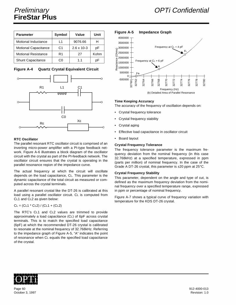
FireStar PlusPreliminary OPTi Confidential
Figure A-4 Quartz Crystal Equivalent Circuit
RTC OscillatorThe parallel resonant RTC oscillator circuit is comprised of aninverting micro-power amplifier with a PI-type feedback net-work. Figure A-6 illustrates a block diagram of the oscillatorcircuit with the crystal as part of the PI-feedback network. Theoscillator circuit ensures that the crystal is operating in theparallel resonance region of the impedance curve.
The actual frequency at which the circuit will oscillatedepends on the load capacitance, CL. This parameter is thedynamic capacitance of the total circuit as measured or com-puted across the crystal terminals.
A parallel resonant crystal like the DT-26 is calibrated at thisload using a parallel oscillator circuit. CL is computed fromCL1 and CL2 as given below:
CL = (CL1 * CL2) / (CL1 + (CL2)
The RTC’s CL1 and CL2 values are trimmed to provideapproximately a load capacitance (CL) of 6pF across crystalterminals. This is to match the specified load capacitance(6pF) at which the recommended DT-26 crystal is calibratedto resonate at the nominal frequency of 32.768kHz. Referringto the impedance graph of Figure A-5, “A” indicates the pointof resonance when CL equals the specified load capacitanceof the crystal.
Figure A-5 Impedance Graph
Time Keeping AccuracyThe accuracy of the frequency of oscillation depends on:
• Crystal frequency tolerance
• Crystal frequency stability
• Crystal aging
• Effective load capacitance in oscillator circuit
• Board layout
Crystal Frequency ToleranceThe frequency tolerance parameter is the maximum fre-quency deviation from the nominal frequency (in this case32.768kHz) at a specified temperature, expressed in ppm(parts per million) of nominal frequency. In the case of theGrade A DT-26 crystal, this parameter is ±20 ppm at 25°C.
Crystal Frequency StabilityThis parameter, dependent on the angle and type of cut, isdefined as the maximum frequency deviation from the nomi-nal frequency over a specified temperature range, expressedin ppm or percentage of nominal frequency.
Figure A-7 shows a typical curve of frequency variation withtemperature for the KDS DT-26 crystal.
Motional Inductance L1 9076.66 H
Motional Capacitance C1 2.6 x 10⁻³ pF
Motional Resistance R1 27 Kohm
Shunt Capacitance C0 1.1 pF
Parameter Symbol Value Unit
R1 L1 C1
C0
REXE
4000000
3500000
3000000
2500000
2000000
1500000
1000000
5000000
-500000
327
60
327
66
327
62
327
64
327
68
327
70
327
72
327
74
327
76
327
78
327
80
FL
A
Fa
Frequency at CL = 6 pF
Frequency at CL = 4 pF
Frequency (Hz)
Rea
ctan
ce (
Ohm
s)
(b) Detailed Area of Parallel Resonance
Page 60 912-4000-013October 3, 1997 Revision: 1.0
OPTi®

FireStar PlusOPTi Confidential Preliminary
Figure A-6 RTC Oscillator Circuit Block Diagram
Figure A-7 Typical Temperature Characteristics
Crystal AgingAs a crystal ages, some frequency shift may be observed.Drift with age is specified to be typically 4 ppm for the firstyear and 2 ppm per year for the life of the KDS DT-26 crystal.
Load CapacitanceFor a parallel resonant calibrated crystal, the crystal manu-facturer specifies the load capacitance at which the crystal
will “parallel” resonate at the nominal frequency. From thegraph of Figure A-8, increasing the effective load capacitanceby hanging additional capacitors on either of the X1 or the X2pin will effectively lower the resonant frequency point “A”toward Fs. The deviation of the frequency Fl with load capac-itance is given by:
FL = FS (1 + C1/2 (C0 + CL))
50M
VDD
21
82C602A RTC
X1 X2
CL2CL1
6pF
DT-26
-90
-80
-70
-60
-50
-40
-30
-20
-10
0
-26
-22
-30
-18
-14
-10 -6 -2 2 6 10 14 18 22 26 30 34 38 42 46 50 54 58 62 66 70 74 78
10
912-4000-013 Page 61Revision: 1.0 October 3, 1997
OPTi®
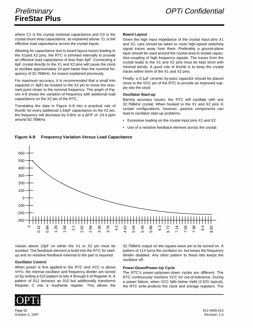
FireStar PlusPreliminary OPTi Confidential
where C1 is the crystal motional capacitance and C0 is thecrystal shunt stray capacitance, as explained above. CL is theeffective load capacitance across the crystal inputs.
Allowing for capacitance due to board layout traces leading tothe X1and X2 pins, the RTC is trimmed internally to providean effective load capacitance of less than 6pF. Connecting a6pF crystal directly to the X1 and X2 pins will cause the clockto oscillate approximately 24 ppm faster than the nominal fre-quency of 32.768kHz, for reason explained previously.
For maximum accuracy, it is recommended that a small trimcapacitor (< 8pF) be hooked to the X2 pin to move the reso-nant point closer to the nominal frequency. The graph of Fig-ure A-8 shows the variation of frequency with additional loadcapacitance on the X2 pin of the RTC.
Translating the data in Figure A-8 into a practical rule ofthumb: for every additional 1.54pF capacitance on the X2 pin,the frequency will decrease by 0.8Hz or a ∆F/F of -24.4 ppmaround 82.768kHz.
Board LayoutGiven the high input impedance of the crystal input pins X1and X2, care should be taken to route high-speed switchingsignal traces away from them. Preferably a ground-planelayer should be used around the crystal area to isolate capac-itive-coupling of high frequency signals. The traces from thecrystal leads to the X1 and X2 pins must be kept short withminimal bends. A good rule of thumb is to keep the crystaltraces within 5mm of the X1 and X2 pins.
Finally, a 0.1µF ceramic by-pass capacitor should be placedclose to the VCC pin of the RTC to provide an improved sup-ply into the clock
Oscillator Start-upBarring accuracy issues, the RTC will oscillate with any32.768kHz crystal. When hooked to the X1 and X2 pins incertain configurations, however, passive components canlead to oscillator start-up problems:
• Excessive loading on the crystal input pins X1 and X2
• Use of a resistive feedback element across the crystal.
Figure A-8 Frequency Variation Versus Load Capacitance
Values above 10pF on either the X1 or X2 pin must beavoided. The feedback element is build into the RTC for start-up and no resistive feedback external to the part is required.
Oscillator ControlWhen power is first applied to the RTC and VCC is aboveVPFD, the internal oscillator and frequency divider are turnedon by writing a 010 pattern to bits 4 through 6 of Register A. Apattern of 011 behaves as 010 but additionally transformsRegister C into a read/write register. This allows the
32.768kHz output on the square-wave pin to be turned on. Apattern of 11X turns the oscillator on, but keeps the frequencydivider disabled. Any other pattern to these bits keeps theoscillator off.
Power-Down/Power-Up CycleThe RTC’s power-up/power-down cycles are different. TheRTC continuously monitors VCC for out-of-tolerance. Duringa power failure, when VCC falls below Vpfd (2.53V typical),the RTC write-protects the clock and storage registers. The
-300
-200
-100
0
100
200
300
400
500
600
0.42
0.840
1.26
1.68 2.1
2.62
2.94
3.36
3.78 4.2
4.62
5.04
5.46
5.88 6.3
6.72
7.14
7.56
7.98 8.4
8.82
Page 62 912-4000-013October 3, 1997 Revision: 1.0
OPTi®

FireStar PlusOPTi Confidential Preliminary
power source is switched to BC when VCC is less than VPFD
and BC is greater than VPFD, or when VCC is less than VBC
and VBC is less than VPFD. RTC operation and storage dataare sustained by a valid back-up energy source. When VCCis above VPFD, the power source is VCC. Write-protectioncontinues for tCSR time after VCC rises above VPFD.
The RTC continuously monitors VCC for out-of-tolerance.During a power failure, when VCC falls below VPFD (4.17Vtypical), the RTC write-protects the clock and storage regis-ters. When VCC is below VBC (3.3V typical), the powersource is switched to BC. RTC operation and storage dataare sustained by a valid back-up energy source. When VCCis above VBC, the power source is VCC. Write-protection con-tinues for tCSR time after VCC rises above VPFD.
Control/Status RegistersThe four control/status registers of the RTC are accessibleregardless of the status of the update cycle (see Table A-7).
Register ARegister A programs the frequency of the periodic event rate,and oscillator operation. Register A provides the status of theupdate cycle. See Table A-8 for Register A’s format.
Register BRegister B enables the update cycle transfer operation,square-wave output-interrupt events, and daylight savingadjustment. Register B selects the clock and calendar dataformats. See Table A-9 for Register B’s format.
Register CRegister C is a read-only event status register. See Table A-10 for Register C’s format.
Register DRegister D is a read-only data integrity status register. SeeTable A-11 for Register D’s format.
Table A-7 Control/Status Registers Summary
Note: NA = Not Affected1. Except Bit 72. Read/write only when OSC[2:0] in Register A is 011 (binary).
Table A-8 Register A
Table A-9 Register B
Reg
iste
r
Loc.
(H
ex)
Rea
d
Writ
e
Bit Name and State on Reset
7 (MSB) 6 5 4 3 2 1 0 (LSB)
A 0A Yes Yes1 UIP NA OSC2 NA OSC1 0 OSC0 0 RS3 NA RS2 NA RS1 NA RS0 NA
B 0B Yes Yes UTI NA PIE 0 AIE 0 UIE 0 SQWE
0 DF NA HF NA DSE NA
C 0C Yes No2 INTF 0 PF 0 AF 0 UF 0 - 0 32KE 0 - 0 - 0
D 0D Yes No VRT NA - 0 - 0 - 0 - 0 - 0 - 0 - 0
Bit(s) Type Function
7 RO UIP - Update-In-Progress: This read-only bit is set prior to the update cycle. When UIP equals 1, an RTC update cycle may be in progress. UIP is cleared at the end of each update cycle. This bit is also cleared when the update transfer inhibit (UTI) bit in Register B is 1.
6:4 R/W OSC[2:0] - Oscillator Control Bits 2 through 0: These three bits control the state of the oscillator and divider stages. A pattern of 010 enables RTC operation by turning on the oscillator and enabling the frequency divider. A pattern of 11X turns the oscillator on, but keeps the frequency divider disabled. When 010 is written, the RTC begins its first update after 500ms.
3:0 R/W RS[3:0] - Rate Select Bits 3 through 0: These bits select one of the 13 frequencies for the SQW output and the periodic interrupt rate, as shown in Table A-4.
Bit(s) Type Function
7 R/W UTI - Update Transfer Inhibit: This bit inhibits the transfer of RTC bytes to the user buffer.
1 = Inhibits transfer and clears UIE0 = Allows Transfer
6 R/W PIE - Periodic Interrupt Enable: This bit enables an interrupt request due to a periodic interrupt event.
1 = Enable0 = Disable
912-4000-013 Page 63Revision: 1.0 October 3, 1997
OPTi®

FireStar PlusPreliminary OPTi Confidential
Table A-10 Register C
Table A-11 Register D
5 R/W AIE - Alarm Interrupt Enable: This bit enables an interrupt request due to an alarm interrupt event.
1 = Enable 0 = Disable
4 R/W UIE - Update Cycle Interrupt Enable: This bit enables an interrupt request due to an update ended interrupt event.
1 = Enable 0 = Disable
The UIE bit is automatically cleared when the UTI bit equals 1.
3 R/W SQWE - Square-Wave Enable: This bit enables the square-wave output.
1 = Enabled 0 = Disabled and held Low
2 R/W DF - Data Format: This bit selects the numeric format in which the time, alarm, and calendar bytes are represented.
1 = Binary 0 = BCD
1 R/W HF - Hour Format: This bit selects the time-of-day and alarm hour format.
1 = 24-hour format 0 = 12-hour format
0 R/W DSE - Daylight Saving Enable: This bit enables daylight saving time adjustments when written to 1.
On the last Sunday in October, the first time the RTC increments past 1:59:59 AM, the time falls back to 1:00:00 am.On the first Sunday in April, the time springs forward from 2:00:00 am to 3:00:00 am.
Bit(s) Type Function
7 R/W INTF - Interrupt Request Flag: This flag is set to a 1 when any of the following is true;
AIE = 1 and AF = 1PIE = 1 and PF = 1UIE = l and UF=1
Reading Register C clears this bit.
6 R/W PF - Periodic Event Flag: This bit is set to a 1 every tPI time, where tPI is the time period selected by the settings of RS[3:0] in Register A. Reading Register C clears this bit.
5 R/W AF - Alarm Event Flag: This bit is set to a 1 when an alarm event occurs. Reading Register C clears this bit.
4 R/W UF - Update Event Flag: This bit is set to a 1 at the end of the update cycle. Reading Register C clears this bit.
3:0 R/W NU - Not Used - This bit is always set to 0.
Bit(s) Type Function
7 RO VRT - Valid RAM and Time:
1 = Valid backup energy source0 = Backup energy source is depleted
When the backup energy source is depleted (VRT = 0), data integrity of the RTC and storage registers is not guaranteed.
6:0 RO NU - Not Used - These bits are always set to 0.
Bit(s) Type Function
Page 64 912-4000-013October 3, 1997 Revision: 1.0
OPTi®

FireStar PlusOPTi Confidential Preliminary
A.2 Signal Definitions
Figure A-9 Notebook Mode A Pin Diagram (100-Pin PQFP)
123456789101112131415161718192021222324252627282930
807978777675747372717069686766656463626160595857565554535251
SD1SD0GNDEPMI1#RSTDRVLLOBAT/KBA20#LOBATEPMI3#/KBRST#XDIRVCCDCS3#RTCWR#RTCRD#DACK7#GNDRQMX1RQMX0PPWR4PPWR3PPWR2PPWR1PPWR0HDCHRDYRTC_5VIRQ8#VBATT32KHZX232KHZX1GNDPPWRL0
100 99 98 97 96 95 94 93 92 91 90 89 88 87 86 85 84 83 82 81
HDRD#HDWR#
GNDHDDSA2
DCS1#IOCHRDY
RINGIDACK0#DACK1#DACK2#DACK3#DACK5#DACK6#
VCCGND
EDACK0EDACK1
RQMX3/RQMX5RQMX2/RQMX4
SUS#/RES#BPWRGDATTRIS#PWRGDATCLK/2
RESETRTCASATCLK
GNDIRQ1IRQ3
31 32 33 34 35 36 37 38 39 40 41 42 43 44 45 46 47 48 49 50
IRQ
10IR
Q12
IRQ
4IR
Q14
IRQ
15R
ES
ET
#E
DA
CK
2E
PM
I2#
SA
5G
ND
VC
CS
A4
SA
3S
A2
SA
1S
A0
ED
AC
KE
NE
PM
I0#
HD
RS
T#
DB
E#
HD
DS
A1
HD
DS
A0
DT
RIS
#X
D7
XD
6X
D5
XD
4X
D3
XD
2V
CC
GN
DX
D1
XD
0LA
TC
HS
D7
SD
6S
D5
SD
4S
D3
SD
2
82C602A
NotebookMode A
912-4000-013 Page 65Revision: 1.0 October 3, 1997
OPTi®
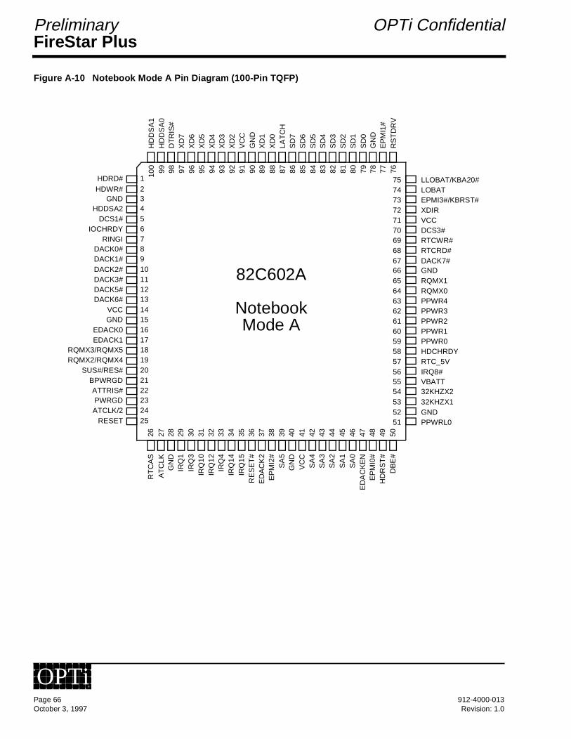
FireStar PlusPreliminary OPTi Confidential
Figure A-10 Notebook Mode A Pin Diagram (100-Pin TQFP)
12345678910111213141516171819202122232425
75747372717069686766656463626160595857565554535251
LLOBAT/KBA20#LOBATEPMI3#/KBRST#XDIRVCCDCS3#RTCWR#RTCRD#DACK7#GNDRQMX1RQMX0PPWR4PPWR3PPWR2PPWR1PPWR0HDCHRDYRTC_5VIRQ8#VBATT32KHZX232KHZX1GNDPPWRL0
HDRD#HDWR#
GNDHDDSA2
DCS1#IOCHRDY
RINGIDACK0#DACK1#DACK2#DACK3#DACK5#DACK6#
VCCGND
EDACK0EDACK1
RQMX3/RQMX5RQMX2/RQMX4
SUS#/RES#BPWRGDATTRIS#PWRGDATCLK/2
RESET
82C602A
NotebookMode A
26 27 28 29 30 31 32 33 34 35 36 37 38 39 40 41 42 43 44 45 46 47 48 49 50
RT
CA
SA
TC
LKG
ND
IRQ
1IR
Q3
IRQ
10IR
Q12
IRQ
4IR
Q14
IRQ
15R
ES
ET
#E
DA
CK
2E
PM
I2#
SA
5G
ND
VC
CS
A4
SA
3S
A2
SA
1S
A0
ED
AC
KE
NE
PM
I0#
HD
RS
T#
DB
E#
767778798081828384858687888990919293949596979899100
RS
TD
RV
EP
MI1
#G
ND
SD
0S
D1
SD
2S
D3
SD
4S
D5
SD
6S
D7
LAT
CH
XD
0X
D1
GN
DV
CC
XD
2X
D3
XD
4X
D5
XD
6X
D7
DT
RIS
#H
DD
SA
0H
DD
SA
1
Page 66 912-4000-013October 3, 1997 Revision: 1.0
OPTi®

FireStar PlusOPTi Confidential Preliminary
Table A-12 Notebook Mode A - Numerical Pin Cross-Reference ListPin Pin Pin Pin Pin Pin Pin Pin
# Pin Name Type1 HDRD# O
2 HDWR# O
3 GND G
4 HDDSA2 O
5 DCS1# O
6 IOCHRDY O
7 RINGI I
8 DACK0# O
9 DACK1# O
10 DACK2# O
11 DACK3# O
12 DACK5# O
13 DACK6# O
14 VCC P
15 GND G
16 EDACK0 I
17 EDACK1 I
18 RQMX3/RQMX5 O
19 RQMX2/RQMX4 O
20 SUS#/RES# I
21 BPWRGD O(OD)
22 ATTRIS# I
23 PWRGD I-Sch
24 ATCLK/2 I
25 RESET I
26 RTCAS I
27 ATCLK I
28 GND G
29 IRQ1 I
30 IRQ3 I
31 IRQ10 I
32 IRQ12 I
33 IRQ4 I
34 IRQ14 I
35 IRQ15 I
36 RESET# O
37 EDACK2 I
38 EPMI2# I
39 SA5 I
40 GND G
41 VCC P
42 SA4 I
43 SA3 I
44 SA2 I
45 SA1 I
46 SA0 I
47 EDACKEN I
48 EPMI0# I
49 HDRST# O
50 DBE# I
# Pin Name Type
51 PPWRL0 I
52 GND G
53 32KHZX1 I
54 32KHZX2 O
55 VBATT I
56 IRQ8# O(OD)
57 RTC_5V I
58 HDCHRDY I
59 PPWR0 O
60 PPWR1 O
61 PPWR2 O
62 PPWR3 O
63 PPWR4 O
64 RQMX0 O
65 RQMX1 O
66 GND G
67 DACK7# O
68 RTCRD# I
69 RTCWR# I
70 DCS3# O
71 VCC P
72 XDIR I
73 EPMI3#/KBRST# I
74 LOBAT I
75 LLOBAT/KBA20# I
# Pin Name Type
76 RSTDRV O
77 EPMI1# I
78 GND G
79 SD0 I/O
80 SD1 I/O
81 SD2 I/O
82 SD3 I/O
83 SD4 I/O
84 SD5 I/O
85 SD6 I/O
86 SD7 I/O
87 LATCH I
88 XD0 I/O
89 XD1 I/O
90 GND G
91 VCC P
92 XD2 I/O
93 XD3 I/O
94 XD4 I/O
95 XD5 I/O
96 XD6 I/O
97 XD7 I/O
98 DTRIS# I
99 HDDSA0 O
100 HDDSA1 O
# Pin Name Type
Table A-13 Notebook Mode A - Alphabetical Pin Cross-Reference ListPin Pin Pin Pin Pin Pin Pin Pin
Pin Name # Type
ATCLK 27 I
ATCLK/2 24 I
ATTRIS# 22 I
BPWRGD 21 O(OD)
DACK0# 8 O
DACK1# 9 O
DACK2# 10 O
DACK3# 11 O
DACK5# 12 O
DACK6# 13 O
DACK7# 67 O
DBE# 50 I
DCS1# 5 O
DCS3# 70 O
DTRIS# 98 I
EDACK0 16 I
EDACK1 17 I
EDACK2 37 I
EDACKEN 47 I
EPMI0# 48 I
EPMI1# 77 I
EPMI2# 38 I
EPMI3#/KBRST# 73 I
GND 3 G
GND 15 G
GND 28 G
GND 40 G
GND 52 G
GND 66 G
GND 78 G
GND 90 G
HDCHRDY 58 I
HDDSA0 99 O
HDDSA1 100 O
HDDSA2 4 O
HDRD# 1 O
HDRST# 49 O
HDWR# 2 O
IOCHRDY 6 O
IRQ1 29 I
IRQ3 30 I
IRQ4 33 I
IRQ8# 56 O(OD)
IRQ10 31 I
IRQ12 32 I
IRQ14 34 I
IRQ15 35 I
LATCH 87 I
LLOBAT/KBA20# 75 I
LOBAT 74 I
Pin Name # Type
PPWR0 59 O
PPWR1 60 O
PPWR2 61 O
PPWR3 62 O
PPWR4 63 O
PPWRL0 51 I
PWRGD 23 I-Sch
RESET 25 I
RESET# 36 O
RINGI 7 I
RQMX0 64 O
RQMX1 65 O
RQMX2/RQMX4 19 O
RQMX3/RQMX5 18 O
RSTDRV 76 O
RTCAS 26 I
RTC_5V 57 I
RTCRD# 68 I
RTCWR# 69 I
SA0 46 I
SA1 45 I
SA2 44 I
SA3 43 I
SA4 42 I
SA5 39 I
Pin Name # Type
SD0 79 I/O
SD1 80 I/O
SD2 81 I/O
SD3 82 I/O
SD4 83 I/O
SD5 84 I/O
SD6 85 I/O
SD7 86 I/O
SUS#/RES# 20 I
VBATT 55 I
VCC 14 P
VCC 41 P
VCC 71 P
VCC 91 P
XD0 88 I/O
XD1 89 I/O
XD2 92 I/O
XD3 93 I/O
XD4 94 I/O
XD5 95 I/O
XD6 96 I/O
XD7 97 I/O
XDIR 72 I
32KHZX1 53 I
32KHZX2 54 O
Pin Name # Type
912-4000-013 Page 67Revision: 1.0 October 3, 1997
OPTi®

FireStar PlusPreliminary OPTi Confidential
A.3 Notebook Mode A Signal DescriptionsRefer to the internal circuitry schematic in Section A.4 for complete details.
A.3.1 Clock and Reset Interface Signals
A.3.2 Interrupt Control Interface Signals
A.3.3 ISA DMA Arbiter Interface Signals
Signal NamePinNo.
SignalType Signal Description
RESET 25 I Reset: Reset input from the FireStar Plus.
RESET# 36 O Reset: The inverted output of RESET (pin 25). This signal is also used to reset the internal real-time clock.
RSTDRV 76 O Reset Drive: An active high reset output to the AT bus.
PWRGD 23 I-Sch Power Good: The PWRGD input signal from the power supply. A rising edge on this input is used to sample the strap information.
BPWRGD 21 O (OD) Buffered Power Good: An open drain output signal to the FireStar Plus.
Signal NamePinNo.
SignalType Signal Description
IRQ1, IRQ3, IRQ10, IRQ12
29, 30, 31, 32
I Interrupt Request bits 1, 3, 10, and 12: Interrupt request inputs from the ISA bus. These inputs are output serially to the FireStar Plus on RQMX0. A low pulse on any of these inputs is internally extended by one ATCLK.
IRQ4, IRQ14, IRQ15
33, 34, 35
I Interrupt Request bits 4, 14, and 15: Interrupt request inputs from the ISA bus. These inputs are output serially to the FireStar Plus along with IRQ8# on RQMX1. A low pulse on any of these inputs is internally extended by one ATCLK.
RQMX[1:0] 65, 64 O Serial Outputs 1 and 0: These outputs are sent to the FireStar Plus. The FireStar Plus will demultiplex these lines to decode interrupt and power man-agement information.
Signal NamePinNo.
SignalType Signal Description
DACK[7:0]# 67, 13:8 O DMA Acknowledge bits 7 through 0: These output signals are directly con-nected to the ISA bus. They are derived from the EDACK[2:0] and EDACKEN inputs from the FireStar Plus.
EDACK[2:0] 37, 17, 16
I Encoded DMA Acknowledge bits 2 through 0: These encoded inputs give a 3-to-8 decode for the DMA acknowledge.
EDACKEN 47 I Encoded DMA Acknowledge Enable: This active high input allows the DACKs to be decoded.
Page 68 912-4000-013October 3, 1997 Revision: 1.0
OPTi®
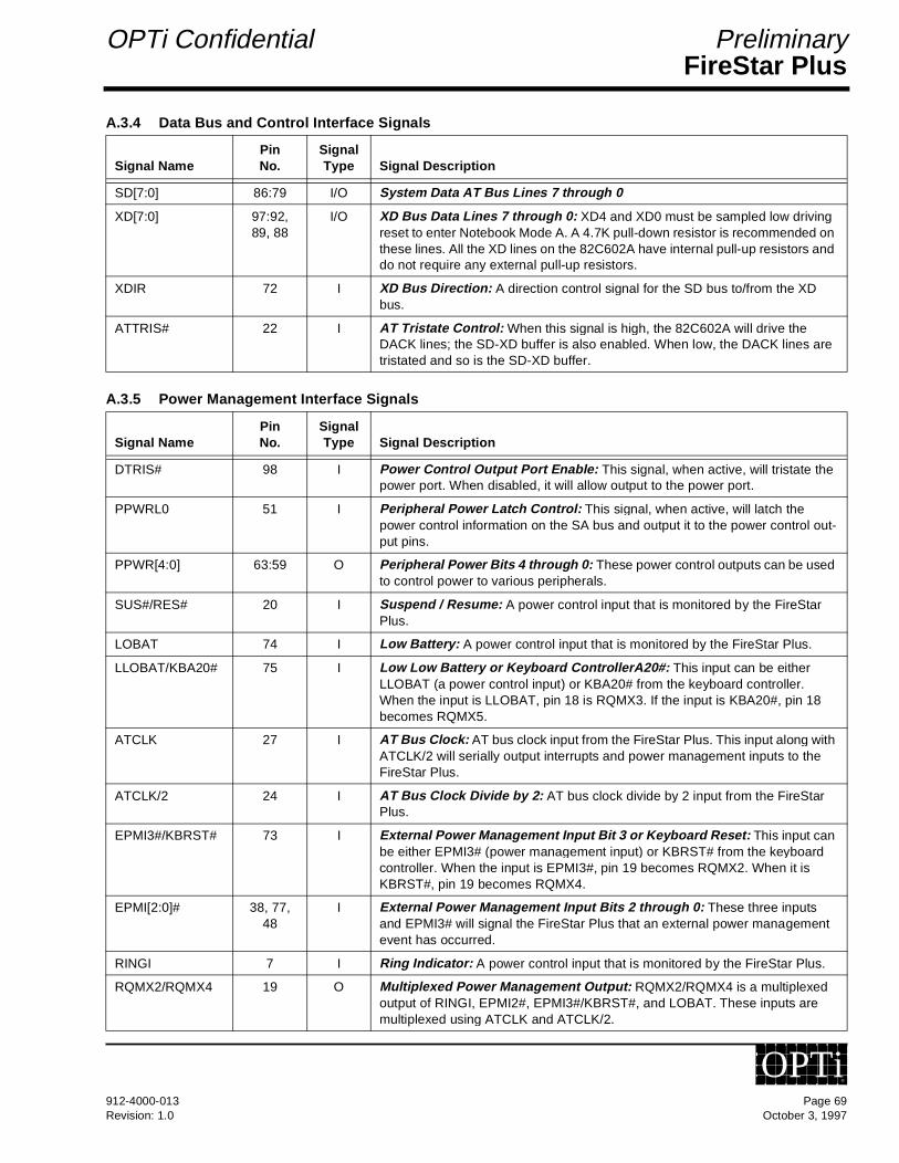
FireStar PlusOPTi Confidential Preliminary
A.3.4 Data Bus and Control Interface Signals
A.3.5 Power Management Interface Signals
Signal NamePinNo.
SignalType Signal Description
SD[7:0] 86:79 I/O System Data AT Bus Lines 7 through 0
XD[7:0] 97:92, 89, 88
I/O XD Bus Data Lines 7 through 0: XD4 and XD0 must be sampled low driving reset to enter Notebook Mode A. A 4.7K pull-down resistor is recommended on these lines. All the XD lines on the 82C602A have internal pull-up resistors and do not require any external pull-up resistors.
XDIR 72 I XD Bus Direction: A direction control signal for the SD bus to/from the XD bus.
ATTRIS# 22 I AT Tristate Control: When this signal is high, the 82C602A will drive the DACK lines; the SD-XD buffer is also enabled. When low, the DACK lines are tristated and so is the SD-XD buffer.
Signal NamePinNo.
SignalType Signal Description
DTRIS# 98 I Power Control Output Port Enable: This signal, when active, will tristate the power port. When disabled, it will allow output to the power port.
PPWRL0 51 I Peripheral Power Latch Control: This signal, when active, will latch the power control information on the SA bus and output it to the power control out-put pins.
PPWR[4:0] 63:59 O Peripheral Power Bits 4 through 0: These power control outputs can be used to control power to various peripherals.
SUS#/RES# 20 I Suspend / Resume: A power control input that is monitored by the FireStar Plus.
LOBAT 74 I Low Battery: A power control input that is monitored by the FireStar Plus.
LLOBAT/KBA20# 75 I Low Low Battery or Keyboard ControllerA20#: This input can be either LLOBAT (a power control input) or KBA20# from the keyboard controller. When the input is LLOBAT, pin 18 is RQMX3. If the input is KBA20#, pin 18 becomes RQMX5.
ATCLK 27 I AT Bus Clock: AT bus clock input from the FireStar Plus. This input along with ATCLK/2 will serially output interrupts and power management inputs to the FireStar Plus.
ATCLK/2 24 I AT Bus Clock Divide by 2: AT bus clock divide by 2 input from the FireStar Plus.
EPMI3#/KBRST# 73 I External Power Management Input Bit 3 or Keyboard Reset: This input can be either EPMI3# (power management input) or KBRST# from the keyboard controller. When the input is EPMI3#, pin 19 becomes RQMX2. When it is KBRST#, pin 19 becomes RQMX4.
EPMI[2:0]# 38, 77, 48
I External Power Management Input Bits 2 through 0: These three inputs and EPMI3# will signal the FireStar Plus that an external power management event has occurred.
RINGI 7 I Ring Indicator: A power control input that is monitored by the FireStar Plus.
RQMX2/RQMX4 19 O Multiplexed Power Management Output: RQMX2/RQMX4 is a multiplexed output of RINGI, EPMI2#, EPMI3#/KBRST#, and LOBAT. These inputs are multiplexed using ATCLK and ATCLK/2.
912-4000-013 Page 69Revision: 1.0 October 3, 1997
OPTi®
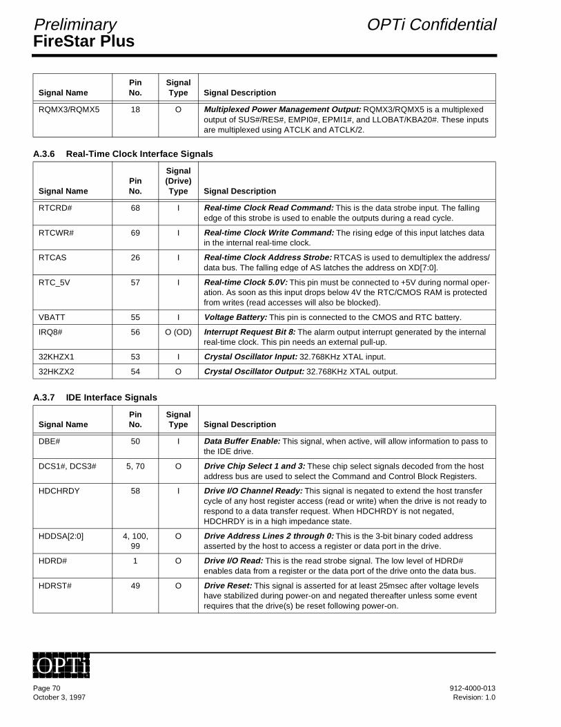
FireStar PlusPreliminary OPTi Confidential
A.3.6 Real-Time Clock Interface Signals
A.3.7 IDE Interface Signals
RQMX3/RQMX5 18 O Multiplexed Power Management Output: RQMX3/RQMX5 is a multiplexed output of SUS#/RES#, EMPI0#, EPMI1#, and LLOBAT/KBA20#. These inputs are multiplexed using ATCLK and ATCLK/2.
Signal NamePinNo.
Signal(Drive)Type Signal Description
RTCRD# 68 I Real-time Clock Read Command: This is the data strobe input. The falling edge of this strobe is used to enable the outputs during a read cycle.
RTCWR# 69 I Real-time Clock Write Command: The rising edge of this input latches data in the internal real-time clock.
RTCAS 26 I Real-time Clock Address Strobe: RTCAS is used to demultiplex the address/data bus. The falling edge of AS latches the address on XD[7:0].
RTC_5V 57 I Real-time Clock 5.0V: This pin must be connected to +5V during normal oper-ation. As soon as this input drops below 4V the RTC/CMOS RAM is protected from writes (read accesses will also be blocked).
VBATT 55 I Voltage Battery: This pin is connected to the CMOS and RTC battery.
IRQ8# 56 O (OD) Interrupt Request Bit 8: The alarm output interrupt generated by the internal real-time clock. This pin needs an external pull-up.
32KHZX1 53 I Crystal Oscillator Input: 32.768KHz XTAL input.
32HKZX2 54 O Crystal Oscillator Output: 32.768KHz XTAL output.
Signal NamePinNo.
SignalType Signal Description
DBE# 50 I Data Buffer Enable: This signal, when active, will allow information to pass to the IDE drive.
DCS1#, DCS3# 5, 70 O Drive Chip Select 1 and 3: These chip select signals decoded from the host address bus are used to select the Command and Control Block Registers.
HDCHRDY 58 I Drive I/O Channel Ready: This signal is negated to extend the host transfer cycle of any host register access (read or write) when the drive is not ready to respond to a data transfer request. When HDCHRDY is not negated, HDCHRDY is in a high impedance state.
HDDSA[2:0] 4, 100, 99
O Drive Address Lines 2 through 0: This is the 3-bit binary coded address asserted by the host to access a register or data port in the drive.
HDRD# 1 O Drive I/O Read: This is the read strobe signal. The low level of HDRD# enables data from a register or the data port of the drive onto the data bus.
HDRST# 49 O Drive Reset: This signal is asserted for at least 25msec after voltage levels have stabilized during power-on and negated thereafter unless some event requires that the drive(s) be reset following power-on.
Signal NamePinNo.
SignalType Signal Description
Page 70 912-4000-013October 3, 1997 Revision: 1.0
OPTi®
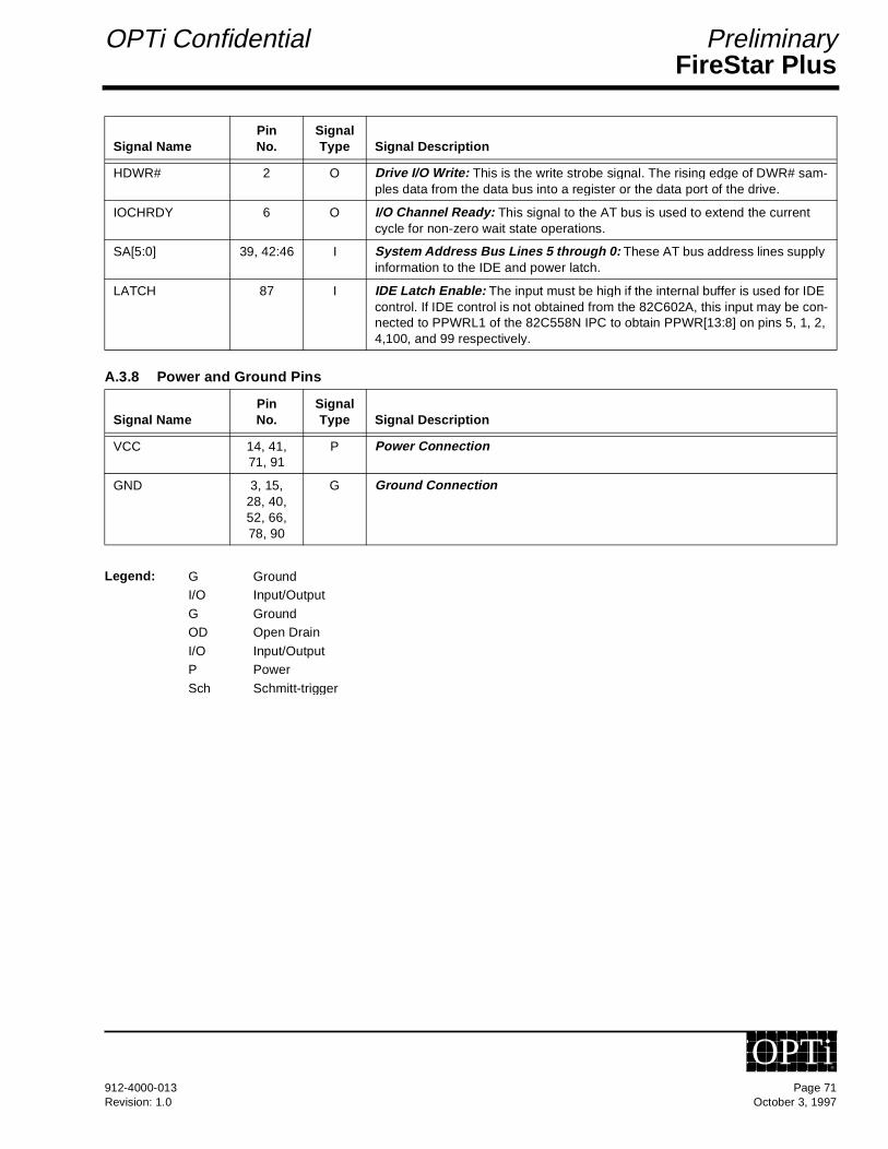
FireStar PlusOPTi Confidential Preliminary
A.3.8 Power and Ground Pins
HDWR# 2 O Drive I/O Write: This is the write strobe signal. The rising edge of DWR# sam-ples data from the data bus into a register or the data port of the drive.
IOCHRDY 6 O I/O Channel Ready: This signal to the AT bus is used to extend the current cycle for non-zero wait state operations.
SA[5:0] 39, 42:46 I System Address Bus Lines 5 through 0: These AT bus address lines supply information to the IDE and power latch.
LATCH 87 I IDE Latch Enable: The input must be high if the internal buffer is used for IDE control. If IDE control is not obtained from the 82C602A, this input may be con-nected to PPWRL1 of the 82C558N IPC to obtain PPWR[13:8] on pins 5, 1, 2, 4,100, and 99 respectively.
Signal NamePinNo.
SignalType Signal Description
VCC 14, 41, 71, 91
P Power Connection
GND 3, 15, 28, 40, 52, 66, 78, 90
G Ground Connection
Legend: G GroundI/O Input/Output
G GroundOD Open Drain
I/O Input/OutputP Power
Sch Schmitt-trigger
Signal NamePinNo.
SignalType Signal Description
912-4000-013 Page 71Revision: 1.0 October 3, 1997
OPTi®

FireStar PlusPreliminary OPTi Confidential
A.4 SchematicsFigure A-11 shows schematics of the internal circuitry when in the Notebook Mode A.
Figure A-11 602A Mode A for FireStar Plus
Page 72 912-4000-013October 3, 1997 Revision: 1.0
OPTi®
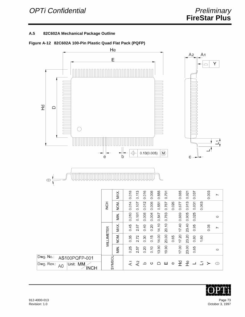
FireStar PlusOPTi Confidential Preliminary
A.5 82C602A Mechanical Package Outline
Figure A-12 82C602A 100-Pin Plastic Quad Flat Pack (PQFP)
912-4000-013 Page 73Revision: 1.0 October 3, 1997
OPTi®
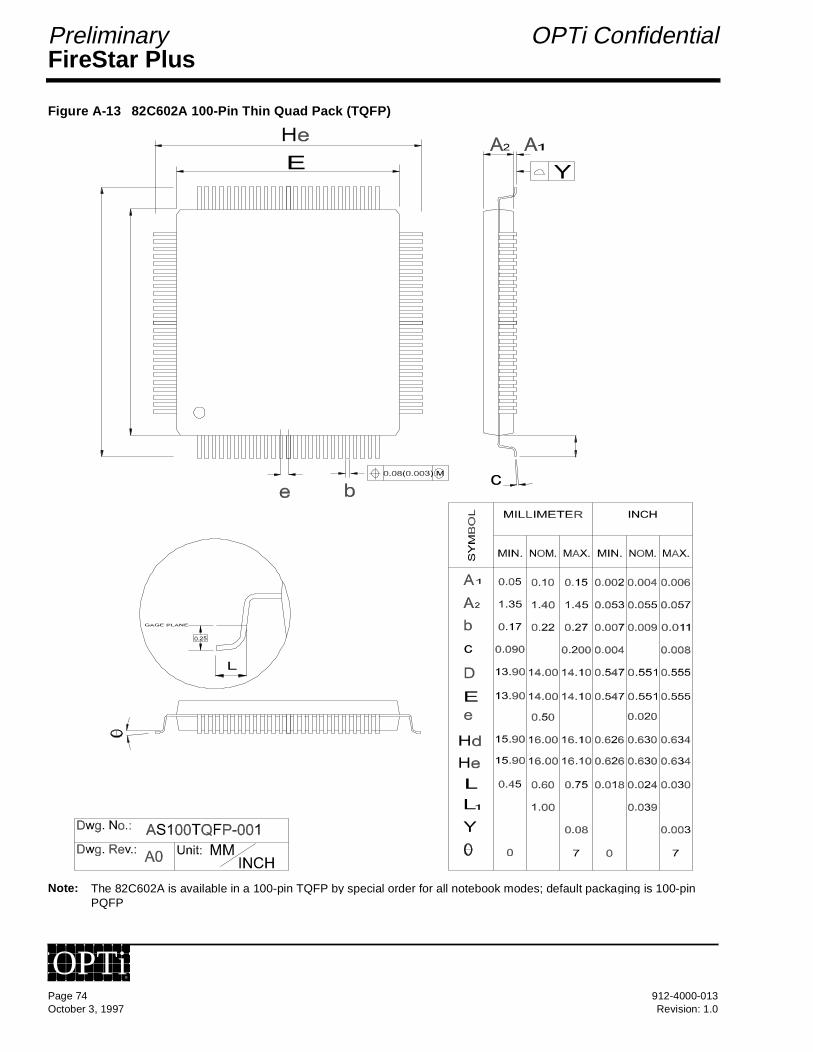
FireStar PlusPreliminary OPTi Confidential
Figure A-13 82C602A 100-Pin Thin Quad Pack (TQFP)
Note: The 82C602A is available in a 100-pin TQFP by special order for all notebook modes; default packaging is 100-pin PQFP
Page 74 912-4000-013October 3, 1997 Revision: 1.0
OPTi®

FireStar PlusOPTi Confidential Preliminary
Appendix B. Register Descriptions
B.1 PCIDV0 Register SpaceThe PCI Configuration Register Space designated asPCIDV0 is accessed through Configuration Mechanism #1 asBus #0, Device #0, and Function #0.
PCIDV0 00h-3Fh are PCI-specific registers while PCIDV040h-FFh are system control related registers. Table B-1 givesthe bit formats for these registers.
Table B-1 PCIDV0 00h-FFh
7 6 5 4 3 2 1 0
PCIDV0 00h Vendor Identification Register (RO) - Byte 0 Default = 45h
PCIDV0 01h Vendor Identification Register (RO) - Byte 1 Default = 10h
PCIDV0 02h Device Identification Register (RO) - Byte 0 Default = 01h
PCIDV0 03h Device Identification Register (RO) - Byte 1 Default = C7h
PCIDV0 04h Command Register - Byte 0 Default = 07h
Address/data stepping (RO):
0 = Disable(always)
PERR# output pin:
0 = Disable(always)
Reserved Memory write and invalidate cycle genera-
tion (RO):
Must = 0 (always)
No memory write and invali-date cycles will be generated by the 82C700.
Special cycles (RO):
Must = 0(always)
The 82C700 does not respond to the PCI special cycle.
Bus master operations
(RO):
Must = 1(always)
This allows the 82C700 to per-form bus master operations at any time.
(Default = 1)
Memory access (RO):
Must = 1(always)
The 82C700 allows a PCI bus master access to mem-ory at anytime.
(Default = 1)
I/O access (RO):
Must = 1(always)
The 82C700 allows a PCI bus master I/O access at any time.
(Default = 1)
PCIDV0 05h Command Register - Byte 1 Default = 00h
Reserved Fast back-to-back to differ-
ent slaves:
0 = Disable1 = Enable
SERR# output pin (RO):
0 = Disable(always)
PCIDV0 06h Status Register - Byte 0 Default = 80h
Fast back-to-back capability
(RO):
0 = Not Capable1 = Capable
(Default = 1)
Also see PCIDV0 46h[2].
Reserved
912-4000-013 Page 75Revision: 1.0 October 3, 1997
OPTi®
FireStar PlusPreliminary OPTi Confidential
PCIDV0 07h Status Register - Byte 1 Default = 00h
Detected parity error:
Must = 0(always)
SERR# status:
Must = 0(always)
Master abort status:
Must = 0(always)
Received tar-get abort status:
0 = No target abort
1 = Target abort occurred
Signaled target abort status:
Must = 0 (always)
DEVSEL# timing status (RO):
Must = 01 (always)
Indicates medium timing selec-tion; the 82C700 asserts the DEVSEL# based on medium timing.
(Default = 01)
Data parity detected:
Must = 0 (always)
PCIDV0 08h Revision Identification Register (RO) Default = 10h
- The chip revision number in the PCI configuration space consists of two parts: a major revision number and a minor revision number. The 8-bit register is interpreted as x.yh, where for example revision 2.1 of the chip would be read as two BCD digits, 0010 0001b. Software programmers must take care in using the minor revision number, because the number may change between register- and software-equivalent versions of the chip.
PCIDV0 09h Class Code Register (RO) - Byte 0 Default = 00h
PCIDV0 0Ah Class Code Register (RO) - Byte 1 Default = 00h
PCIDV0 0Bh Class Code Register (RO) - Byte 2 Default = 06h
PCIDV0 0Ch Reserved Default = 00h
PCIDV0 0Dh Master Latency Timer Register (RO) Default = 00h
PCIDV0 0Eh Header Type Register (RO) Default = 00h
PCIDV0 0Fh Built-In Self-Test (BIST) Register (RO) Default = 00h
PCIDV0 10h-2Bh Reserved Default = 00h
PCIDV0 2Ch-2Dh Subsystem Vendor ID Default = 00h
(Write one time only)
PCIDV0 2Eh-2Fh Subsystem ID Default = 00h
(Write one time only)
PCIDV0 30h-3Fh Reserved Default = 00h
Table B-1 PCIDV0 00h-FFh (cont.)
7 6 5 4 3 2 1 0
Page 76 912-4000-013October 3, 1997 Revision: 1.0
OPTi®

FireStar PlusOPTi Confidential Preliminary
PCIDV0 40h Memory Control Register - Byte 0 Default = 00h
PCI video frame buffer write posting hole:
These bits map onto address bits A[31:30]. Together with PCIDV0 41h[7:0] they define the 4MB win-dow where write posting can be masked.
Reserved Reserved 0 = Control of writes being posted on PCI bus is determined by SYSCFG 15h[5:4].
1 = No writes will be posted on PCI bus except writes to video mem-ory and frame buffer areas.
Also see bits 2 and 1.
Write posting to the video frame buffer control:
If bit 3 = 0:0 = Enable1 = Disable
If bit 3 = 1:0 = Disable1 = Enable
Write posting to the video mem-
ory (A0000h-BFFFFh) control:
If bit 3 = 0:0 = Enable 1 = Disable
If bit 3 = 1:0 = Disable1 = Enable
I/O cycle write post control:
0 = Disable1 = Enable
PCIDV0 41h Memory Control Register - Byte 1 Default = 00h
PCI video frame buffer write posting hole:
- These bits map onto address bits A[29:22].- Together with PCIDV0 40h[7:6] they define the 4MB window where write posting can be masked.
PCIDV0 42h Memory Control Register - Byte 2 Default = 00h
Reserved. This bit must be set to 1 to
correct improper opera-
tion while switching between
DRAM banks.
Allow HA drive-back during
CPU memory accesses:
0 = Disable1 = Enable
PCIDV0 43h Internal Project Revision - Reserved Default = 20h
PCIDV0 44h Data Path Register 1 Default = 00h
6DW FIFO for CPU write to
PCI:
0 = Disable1 = Enable
16QW FIFO for PCI read from
DRAM:
0 = Disable1 = Enable
16QW FIFO for PCI write to
DRAM:
0 = Disable1 = Enable
6QW FIFO for CPU write to
DRAM:
0 = Disable1 = Enable
Memory read accesses in
DBC if PCIDV0 44h[0] = 1 and
47h[7] = 1:
0 = SDRAM1 = Reserved
DBC ping-pong buffer used for
PCI master write
X-1-1-1:
0 = Disable1 = Enable
DBC ping-pong buffer used for
PCI master read
X-1-1-1:
0 = Disable1 = Enable
Memory read accesses in the
DBC:
0 = FP Mode1 = EDO/
SDRAM
Table B-1 PCIDV0 00h-FFh (cont.)
7 6 5 4 3 2 1 0
912-4000-013 Page 77Revision: 1.0 October 3, 1997
OPTi®
FireStar PlusPreliminary OPTi Confidential
PCIDV0 45h Data Path Control Register 2 Default = 00h
Reserved Ping-pong buffer reset of
CPU read EDO is qualified with
HDOE#.
0 = Disable1 = Enable
When IADV# = 0, BE[7:0]# are forced to 00h
for write (CPU-to-DRAM and CPU-to-PCI) cycle control.
0 = Disable1 = Enable
Reserved Reserved. Byte merge for CPU write to
DRAM:
0 = Disable1 = Enable
Reserved
PCIDV0 46h Data Path Control Register 3 Default = 00h
Reserved: Write to 0
PCIDV0 47h Data Path Control Register 4 Default = 00h
SDRAM memory read accesses in
DBC:
0 = Disable1 = Enable
CPU-to-PCI FIFO clearing
when combina-tion changed:
0 = Do not clear1 = Clear
PCI-to-DRAM FIFO clearing
when combina-tion changed:
0 = Do not clear1 = Clear
CPU-to-DRAM FIFO clearing
when combina-tion changed:
0 = Do not clear1 = Clear
82C700 regis-ter is writable:
0 = Enable
1 = Disable (cnfg-writes
blocked within DBC)
New DLE# gen-eration during
64-bit PCI read/write.
0 = Disable1 = Enable
Reserved
PCIDV0 48h Data Path Control Register 5 Default = 00h
Reserved During refresh cycles if this bit = 1, the RAS# corresponding
to the bank with size 0 will not be generated for SDRAM.
Aggressive SDCAS#/
SDRAS# step-ping.
0 = Disable1 = Enable
Reserved SDRAM mode select
000 = Normal SDRAM mode001 = NOP command enable010 = All banks precharge011 = Mode register command enable100 = CBR cycle enableAll other combinations = Reserved
PCIDV0 49h-4Bh Reserved Default = 00h
PCIDV0 4Ch MCACHE Control Register Default = 00h
Reserved. Enable GWE#/BWE L2 cache interface
0 = Disable1 = Enable
Reserved Reserved Reserved. Set to 1 whenever
ISA retry is enabled
Reserved MA13 function-ality on the TDI
pin
0 = Disable1 = Enable
Reserved
PCIDV0 4Dh Delay Adjustment Register Default = 00h
Reserved Reserved SDRAM bank 5 enable/disable
0 = Disable1 = Enable
SDRAM bank 4 enable/disable
0 = Disable1 = Enable
Reserved Internal DLE0# delay adjustment for DRAM read:
00 = I/O buffer delay01 = 6ns10 = 3ns11 = No delay
Reserved
Table B-1 PCIDV0 00h-FFh (cont.)
7 6 5 4 3 2 1 0
Page 78 912-4000-013October 3, 1997 Revision: 1.0
OPTi®
FireStar PlusOPTi Confidential Preliminary
PCIDV0 4Eh SDRAM Control Register 1 Default = 00h
Enable DTYI delay when
SDRAM + L2 + Piping enabled
0 = Disabled
1 = Enabled
Reserved Reserved
PCIDV0 4Fh-53h Reserved Default = 00h
PCIDV0 54h SDRAM Control Register 2 Default = 00h
SDRAM 16/64 Mbit slect for
bank 10 = 16Mb1 = 64Mb
SDRAM 16/64 Mbit slect for
bank 00 = 16Mb1 = 64Mb
SDRAM leadoff timing for Bank
50 = 7 CLK
leadoff1 = 8 CLk
leadoff
SDRAM leadoff timing for Bank
40 = 7 CLK
leadoff1 = 8 CLk
leadoff
SDRAM leadoff timing for Bank
30 = 7 CLK
leadoff1 = 8 CLk
leadoff
SDRAM leadoff timing for Bank
20 = 7 CLK
leadoff1 = 8 CLk
leadoff
SDRAM leadoff timing for Bank
10 = 7 CLK
leadoff1 = 8 CLk
leadoff
SDRAM leadoff timing for Bank
00 = 7 CLK
leadoff1 = 8 CLk
leadoff
PCIDV0 55h SDRAM Control Register 3 Default = 00h
Aggressive stepping of
DWE for SDRAM write
cycles
0 = Disable stepping
1 = Enable Stepping
SDRAM and hidden refresh
fix
0 = Disable fix
1 = Enable fix
Reserved. Set this bit to 1, only
if there is no EDO in the sys-
tem
Reserved SDRAM 16/64 Mbit slect for
bank 5
0 = 16Mb
1 = 64Mb
SDRAM 16/64 Mbit slect for
bank 4
0 = 16Mb
1 = 64Mb
SDRAM 16/64 Mbit slect for
bank 3
0 = 16Mb
1 = 64Mb
SDRAM 16/64 Mbit slect for
bank 2
0 = 16Mb
1 = 64Mb
PCIDV0 56h Reserved Default = 00h
PCIDV0 57h ISA retry Register Default = 00h
Handling of BOFF# genera-
tion when a retry occurs
with a pending Master request
0 = Through tar-get abort
1 = Extends retry timer dur-
ing master cycle
BOFF# genera-tion for any PCI/ISA cycle retry
0 = Disable
1 = Enable
BOFF# genera-tion irrespec-
tive of operation
underway if retry
0 = Disable
1 = Enable
Double syn-chronization of PCI cycle indi-
cator for BOFF# generation
0 = Disable
1 = Enable
AHOLD genera-tion for all
retried PCI write cycles
0 = Disable
1 = Enable
Fix for Odd words being
dropped during a retry of a 64bit
PCI write
0 = Disable
1 = Enable
Reserved
PCIDV0 58h-FFh Reserved Default = 00h
Table B-1 PCIDV0 00h-FFh (cont.)
7 6 5 4 3 2 1 0
912-4000-013 Page 79Revision: 1.0 October 3, 1997
OPTi®

FireStar PlusPreliminary OPTi Confidential
B.2 SYSCFG Register SpaceAn indexing scheme is used to access the System ControlRegister Space (SYSCFG). Port 022h is used as the IndexRegister and Port 024h as the Data Register. Each access toa register within this space consists of:
1) a write to Port 022h, specifying the desired register in thedata byte,
2. followed by a read or write to Port 024h with the actualregister data.
The index resets after every access; so every data access(via Port 024h) must be preceded by a write to Port 022heven if the same register is being accessed consecutively.
Port 023h is the Data Register for DMA clock select.
Table B-3 gives the bit formats for the registers located atSYSCFG 00h-2Fh. Table B-4 gives the bit formats for theregisters located at SYSCFG 30h-FFh which are the powermanagement registers.
B.2.1 System Configuration Register Index/Data Programmable
The SYSCFG index/data ports default to 022h/024h as inprevious OPTi chipsets, but now these registers are accessi-ble at other locations as well. PCIDV1 5Fh is provided to pro-gram the upper bits of the index/data port I/O address. Theseregister bits default to 0, leaving the traditional 022h/024hlocations as index/data. Refer to Table B-2.
Table B-2 SYSCFG Base Select Register
7 6 5 4 3 2 1 0
PCIDV1 5Fh Config. Register Index/ Data Port Address
Configuration Register Index/Data Port Address bits A[15:8]:
This byte provides the upper address bits of the 16-bit address for the system configuration registers index/data port. Bits A[7:0] always point to 022h/024h. At reset this register defaults to 0, so the full I/O address for the index/data ports is 0022/0024h.
Table B-3 SYSCFG 00h-2Fh
7 6 5 4 3 2 1 0
SYSCFG 00h Byte Merge/Prefetch & Sony Cache Module Control Register Default = 00h
Enable pipelin-ing of single
CPU cycles to memory:
0 = Disable1 = Enable
SDRAM pipelin-ing fix. This bit needs to be set to 1, before set-ting SYSCFG 29h[7] = 1
0 = Disable1 = Enable
fix
Reserved. Set to 0 always
Reserved. Set to 0 always
Reserved. Set to 0 always
Reserved. Set to 00 always. Reserved. Set to 0 always
SYSCFG 01h DRAM Control Register 1 Default = 00h
Row address HOLD after
RAS# active:
0 = 2 CPUCLKs1 = 1 CPUCLK
RAS# active/inactive when
starting a master cycle:
0 = RAS inac-tive
1 =RAS active
RAS pulse width used during refresh:
00 = 7 CPUCLKs01 = 6 CPUCLKs10 = 5 CPUCLKs11 = 4 CPUCLKs
CAS pulse width during
reads:
0 = 3 CPUCLKs1 = 2 CPUCLKs
For 1 CPUCLK width, refer to SYSCFG 1Ch[0].
CAS pulse width during
writes:
0 = 3 CPUCLKs1 = 2 CPUCLKs
RAS precharge time:
00 = 6 CPUCLKs01 = 5 CPUCLKs10 = 4 CPUCLKs11 = 3 CPUCLKs
Page 80 912-4000-013October 3, 1997 Revision: 1.0
OPTi®
FireStar PlusOPTi Confidential Preliminary
SYSCFG 02h Cache Control Register 1 Default = 00h
L2 cache size selection:
If SYSCFG If SYSCFG0Fh[0] = 0 0Fh[0] = 100 = 64KB 00 = 1MB01 = 128KB 01 = Reserved10 = 256KB 10 = Reserved11 = 512KB 11 = Reserved
L2 cache write policy:
00 = L2 cache write-through01 = Adaptive writeback Mode 110 = Adaptive writeback Mode 211 = L2 cache writeback
L2 cache operating mode select:
00 = Disable
01 = Test Mode 1; External Tag Write (Tag data write-through SYSCFG 07h)
10 = Test Mode 2; External Tag Read (Tag data read from SYSCFG 07h)
11 = Enable L2 cache
DRAM posted write:
0 = Disable1 = Enable
CAS precharge time:
0 = 2 CPUCLKs1 = 1 CPUCLK
SYSCFG 03h Cache Control Register 2 Default = 00h
Timing for burst writes to L2 cache:
00 = X-4-4-4 10 = X-2-2-201 = X-3-3-3 11 = X-1-1-1
Leadoff cycle time for writes to L2 cache:
00 = 5-X-X-X 10 = 3-X-X-X01 = 4-X-X-X 11 = 2-X-X-X
Timing for burst reads to L2 cache:
00 = X-4-4-4 10 = X-2-2-201 = X-3-3-3 11 = X-1-1-1
Leadoff cycle time for reads to L2 cache:
00 = 5-X-X-X 10 = 3-X-X-X01 = 4-X-X-X 11 = 2-X-X-X
SYSCFG 04h Shadow RAM Control Register 1 Default = 00h
CC000h-CFFFFh read/write control:
00 = Read/write PCI bus
01 = Read from DRAM/write to PCI
10 = Read from PCI/write to DRAM
11 = Read/write DRAM
C8000h-CBFFFh read/write control:
00 = Read/write PCI bus
01 = Read from DRAM/write to PCI
10 = Read from PCI/write to DRAM
11 = Read/write DRAM
Sync SRAM pipelined read cycle 1-1-1-1
enable:(1)
0 = Implies leadoff T-state for read pipe-lined cycle = 2(2)
1 = Enables leadoff T-state for read pipe-lined cycle = 1(3)
E0000h-EFFFFh range
selection:
Determines whether this region will be treated like the F0000 BIOS area or whether it will always be non-cacheable.
0 = E0000h-EFFFFh area will always be non-cache-able
1 = E0000h-EFFFFh area will be treated like the F0000h BIOS area.
If this bit is set, then SYSCFG 06h[3:2] and [1:0] Should be set identically.
C0000h-C7FFFh read/write control:
00 = Read/write PCI bus
01 = Read from DRAM/write to PCI
10 = Read from PCI/write to DRAM
11 = Read/write DRAM
(1) If SYSCFG 03h[3:2] = 11, then this register setting is valid.
(2) It will be a 3-1-1-1 cycle followed by a 2-1-1-1 cycle, or a 3-1-1-1 cycle for successive pipelined cycles, based on SYSCFG 10h[5].
(3) It will be a 3-1-1-1 cycle followed by a 1-1-1-1 cycle for successive pipelined cycles. SYSCFG 10h[5] must be set to 1.
Table B-3 SYSCFG 00h-2Fh (cont.)
7 6 5 4 3 2 1 0
912-4000-013 Page 81Revision: 1.0 October 3, 1997
OPTi®
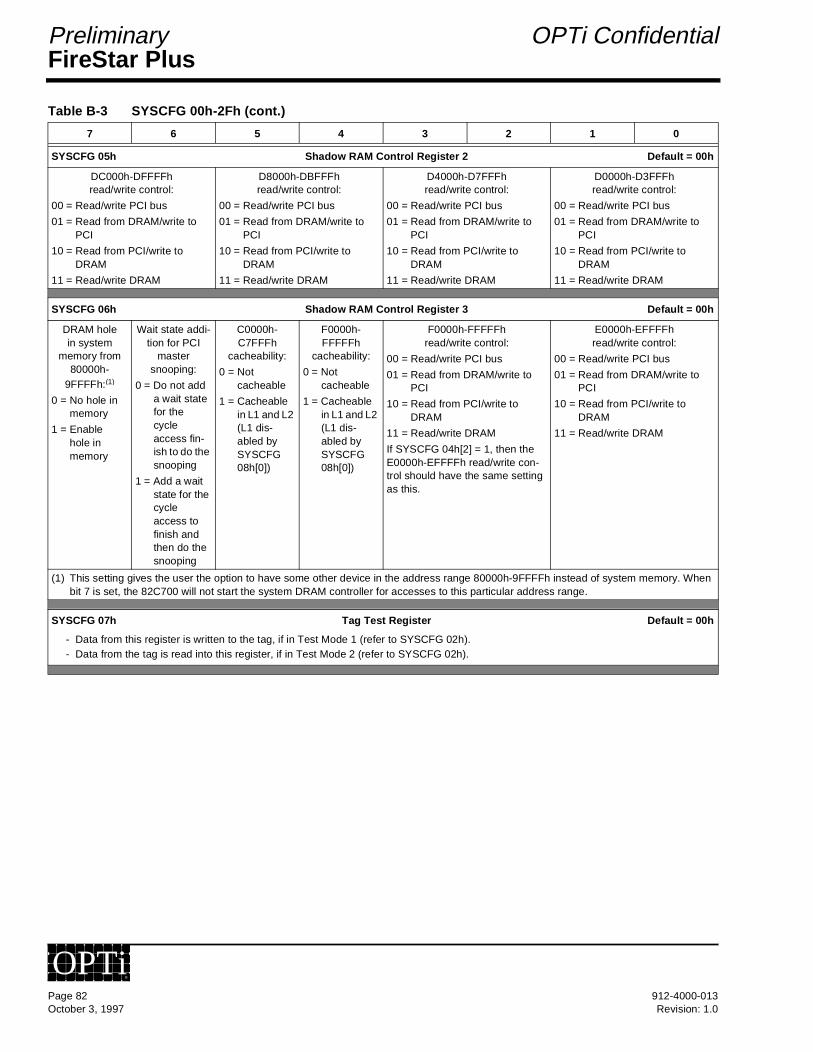
FireStar PlusPreliminary OPTi Confidential
SYSCFG 05h Shadow RAM Control Register 2 Default = 00h
DC000h-DFFFFhread/write control:
00 = Read/write PCI bus
01 = Read from DRAM/write to PCI
10 = Read from PCI/write to DRAM
11 = Read/write DRAM
D8000h-DBFFFhread/write control:
00 = Read/write PCI bus
01 = Read from DRAM/write to PCI
10 = Read from PCI/write to DRAM
11 = Read/write DRAM
D4000h-D7FFFhread/write control:
00 = Read/write PCI bus
01 = Read from DRAM/write to PCI
10 = Read from PCI/write to DRAM
11 = Read/write DRAM
D0000h-D3FFFhread/write control:
00 = Read/write PCI bus
01 = Read from DRAM/write to PCI
10 = Read from PCI/write to DRAM
11 = Read/write DRAM
SYSCFG 06h Shadow RAM Control Register 3 Default = 00h
DRAM hole in system
memory from 80000h-
9FFFFh:(1)
0 = No hole in memory
1 = Enable hole in memory
Wait state addi-tion for PCI
master snooping:
0 = Do not add a wait state for the cycle access fin-ish to do the snooping
1 = Add a wait state for the cycle access to finish and then do the snooping
C0000h-C7FFFh
cacheability:
0 = Not cacheable
1 = Cacheable in L1 and L2 (L1 dis-abled by SYSCFG 08h[0])
F0000h-FFFFFh
cacheability:
0 = Not cacheable
1 = Cacheable in L1 and L2 (L1 dis-abled by SYSCFG 08h[0])
F0000h-FFFFFh read/write control:
00 = Read/write PCI bus
01 = Read from DRAM/write to PCI
10 = Read from PCI/write to DRAM
11 = Read/write DRAM
If SYSCFG 04h[2] = 1, then the E0000h-EFFFFh read/write con-trol should have the same setting as this.
E0000h-EFFFFh read/write control:
00 = Read/write PCI bus
01 = Read from DRAM/write to PCI
10 = Read from PCI/write to DRAM
11 = Read/write DRAM
(1) This setting gives the user the option to have some other device in the address range 80000h-9FFFFh instead of system memory. When bit 7 is set, the 82C700 will not start the system DRAM controller for accesses to this particular address range.
SYSCFG 07h Tag Test Register Default = 00h
- Data from this register is written to the tag, if in Test Mode 1 (refer to SYSCFG 02h).- Data from the tag is read into this register, if in Test Mode 2 (refer to SYSCFG 02h).
Table B-3 SYSCFG 00h-2Fh (cont.)
7 6 5 4 3 2 1 0
Page 82 912-4000-013October 3, 1997 Revision: 1.0
OPTi®

FireStar PlusOPTi Confidential Preliminary
SYSCFG 08h CPU Cache Control Register Default = 00h
Cache single/double bank
selected.
0 =Double bank L2 config-uration chosen
1 =Single bank L2 config-uration chosen
Snoop filtering for bus
masters:(1)
0 = Disable1 = Enable
CPU HITM# pin sample
timing:
0 = Delay 1 CLK (HITM# sampled on 3rd rising edge of PCICLK after EADS# assertion)
1 = No delay (HITM# sampled on 2nd rising edge of PCICLK after EADS# assertion)
Parity checking:
0 = Disable1 = Enable
Not supported.
Tag and Dirty on the same/dif-
ferent chip.
0 = Tag and Dirty RAM are on separate chips
1 = Tag and Dirty are on the same chip
CPU address pipelining for DRAM burst
cycles:
0 = Disable
1 = Enable(Allow: X-2-2-2-3-2-2-2if SYSCFG 1Fh[5] = 1orX-2-2-2-2-2-2-2if SYSCFG1Fh[5] = 0orX-2-2-2-X-2-2-2if SYSCFG 1Fh[5] = 0 and11[4] = 1)
L1 cache writeback and write-through
control:
0 = Write-through only
1 = Writeback enabled
BIOS area cacheability in
L1 cache:
Determines if system BIOS area E0000h-FFFFFh (if SYSCFG 04h[2] = 1) or F0000h-FFFFFh (if SYSCFG 04h[2] = 0), and video BIOS area C0000h-C7FFFh is cacheable in L1 or not.
0 = Cacheable
1 = NotCacheable
(1) For a master request if the subsequent read/write is within the same cache line, CPU 'Inquire' cycles are not done until there is a cache line miss (i.e., line comparator not activated for accesses within the same cache line).
SYSCFG 09h System Memory Function Register Default = 00h
DRAM Hole B size:
00 = 512KB 10 = 2MB01 = 1MB 11 = 4MB
Address for this hole is specified in SYSCFG 0Bh[7:0] and 0Ch[3:2]
DRAM Hole B control mode:
00 = Disable01 = WT for L1 and L210 = Non-cacheable for L1 and L211 = Enable hole in DRAM
DRAM Hole A size:
00 = 512KB 10 = 2MB01 = 1MB 11 = 4MB
Address for this hole is specified in SYSCFG 0Ah[7:0] and 0Ch[1:0]
DRAM Hole A control mode:
00 = Disable01 = WT for L1 and L210 = Non-cacheable for L1 and L211 = Enable hole in DRAM
SYSCFG 0Ah DRAM Hole A Address Decode Register Default = 00h
DRAM Hole A starting address:
- These bits along with SYSCFG 0Ch[1:0] are used to specify the starting address of DRAM Hole A.- These bits, AST[7:0], map onto HA[26:19] lines.
SYSCFG 0Bh DRAM Hole B Address Decode Register Default = 00h
DRAM Hole B starting address:
- These bits along with SYSCFG 0Ch[3:2] are used to specify the starting address of DRAM Hole B. - These bits, BST[7:0], map onto HA[26:19] lines.
SYSCFG 0Ch DRAM Hole Higher Address Default = 00h
Reserved. Set to 0 always.
Fast BRDY# generation for DRAM write page hits.
BRDY# for DRAM writes generated on:
0 = 4th CPUCLK1 = 3rd CPUCLK
Reserved. Set to 0 always
Reserved. Set to 0 always.
DRAM Hole B starting address:
These bits are used in conjunction with the bits in SYSCFG 0Bh to specify the starting address of DRAM Hole B. These bits, BST[9:8], map onto HA[28:27].
DRAM Hole A starting address:
These bits are used in conjunction with the bits in SYSCFG 0Ah to specify the starting address of DRAM Hole A. These bits, AST[9:8], map onto HA[28:27].
Table B-3 SYSCFG 00h-2Fh (cont.)
7 6 5 4 3 2 1 0
912-4000-013 Page 83Revision: 1.0 October 3, 1997
OPTi®
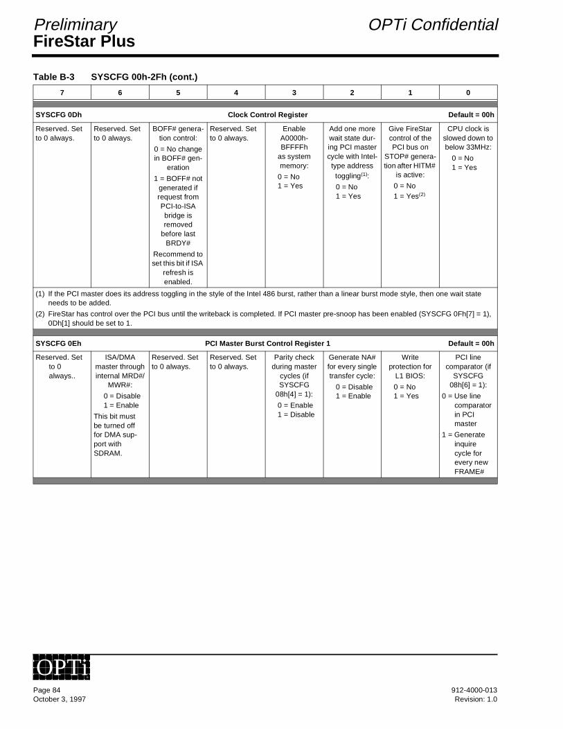
FireStar PlusPreliminary OPTi Confidential
SYSCFG 0Dh Clock Control Register Default = 00h
Reserved. Set to 0 always.
Reserved. Set to 0 always.
BOFF# genera-tion control:
0 = No change in BOFF# gen-
eration
1 = BOFF# not generated if request from PCI-to-ISA bridge is removed
before last BRDY#
Recommend to set this bit if ISA
refresh is enabled.
Reserved. Set to 0 always.
Enable A0000h-BFFFFh
as system memory:
0 = No1 = Yes
Add one more wait state dur-ing PCI master cycle with Intel-type address toggling(1):
0 = No1 = Yes
Give FireStar control of the PCI bus on
STOP# genera-tion after HITM#
is active:
0 = No1 = Yes(2)
CPU clock is slowed down to below 33MHz:
0 = No1 = Yes
(1) If the PCI master does its address toggling in the style of the Intel 486 burst, rather than a linear burst mode style, then one wait state needs to be added.
(2) FireStar has control over the PCI bus until the writeback is completed. If PCI master pre-snoop has been enabled (SYSCFG 0Fh[7] = 1), 0Dh[1] should be set to 1.
SYSCFG 0Eh PCI Master Burst Control Register 1 Default = 00h
Reserved. Set to 0 always..
ISA/DMA master through internal MRD#/
MWR#:
0 = Disable1 = Enable
This bit must be turned off for DMA sup-port with SDRAM.
Reserved. Set to 0 always.
Reserved. Set to 0 always.
Parity check during master
cycles (if SYSCFG
08h[4] = 1):
0 = Enable 1 = Disable
Generate NA# for every single transfer cycle:
0 = Disable1 = Enable
Write protection for
L1 BIOS:
0 = No1 = Yes
PCI line comparator (if
SYSCFG 08h[6] = 1):
0 = Use line comparator in PCI master
1 = Generate inquire cycle for every new FRAME#
Table B-3 SYSCFG 00h-2Fh (cont.)
7 6 5 4 3 2 1 0
Page 84 912-4000-013October 3, 1997 Revision: 1.0
OPTi®

FireStar PlusOPTi Confidential Preliminary
SYSCFG 0Fh PCI Master Burst Control Register 2 Default = 00h
PCI pre-snoop:
0 = Disable1 = Enable(1)
Also see SYSCFG 0Dh[1].
Insert wait states for ISA
master access:
0 = No1 = Yes
CPU-to-DRAM deep buffer in L2 WT mode:
0 = Disable1 = Enable
0 = Default method
1 = If internal PCICYC and BKFRAME are active, retry the PCI cycle block EADS# generation.
New mode of single cycle
NA#:
0 =No change in cache write
hit timing
1 =Cache write hit single trans-fer cycles will
take 3 CLKS to comple if the line is already
dirty
Generate ADSC# for
sync SRAM 1 clock after CPU ADS# in read
cycle:
0 = No1 = Yes(2)
Reserved. Set to 0 always.
Cache size selection:
This bit along with SYSCFG 02h[1:0] defines the L2 cache size.
0 = < 1MB1 = 1MB
(1) FireStar generates a pre-snoop cycle to the CPU assuming that the PCI master will do a burst.
(2) SYSCFG 0Fh[2] needs to be set if pipelined sync SRAMs are being used.
SYSCFG 10h Miscellaneous Control Register 1 Default = 00h
CPU to PCI/ISA slave cycle
triggered:
0 = After 2nd T21 = After 1st T2
Cache modified write cycle
timing:
0 = No delay on CA4
1 = CA4 is delayed one-half clock
Leadoff cycle for a pipelined
read:
0 = 3-X-X-X read followed by a 3-X-X-X pipelined read cycle
1 = 3-X-X-X read followed by a 2-X-X-X pipelined read cycle
2-X-X-X pipelined write
hit cycles:
0 = Disable1 = Enable
Move the write pulse one-half a clock later in X-2-2-2 write
hit cycles:
0 = No1 = Yes
Move the write pulse one-half
a clock earlier in 3-X-X-X write
hit cycles:
0 = No1 = Yes
Reserved PCICLK select control:(1)
0 = PCICLK is async to CPUCLK
1 = PCICLK is sync to CPUCLK
(1) If bit 0 is set, (i.e., sync PCI implementation) then the timing constraints between the PCICLK and CPUCLK inputs to FireStar must be met. PCICLK <= CPUCLK/2 period before CPUCLK PCICLK <= 0.5ns after CPUCLK. Note that in the sync PCICLK option, PCICLK = CPUCLK/2.
SYSCFG 11h Miscellaneous Control Register 2 Default = 00h
Reserved Cache inactive during Idle
state control: This bit con-trols the chip selects of the
SRAMs.
0 = SRAM active always
1 = SRAM inactive dur-ing Idle state
CPU address pipelining for DRAM burst
cycles:
0 = Controlled by SYSCFG 08h[2] and
1F[5]
1 = Slow pipe-lining (allow X-2-2-2-X-2-2-2
when SYSCFG 08h[2] = 1 and
1F[5] = 0
L2 cache type:
0 = No SRAM
1 = Sync. SRAM
This bit should be set to 1 by the BIOS, if L2 cache is being used in the sys-tem
Page miss posted write:
0 = Enable1 = Disable
ATWLRDYB used to block
CSX when BOFFX
Delay start:
0 = Do not delay inter-nal master cycles after an inquire cycle
1 = Delay inter-nal master cycles by 1 PCICLK after inquire cycle
Table B-3 SYSCFG 00h-2Fh (cont.)
7 6 5 4 3 2 1 0
912-4000-013 Page 85Revision: 1.0 October 3, 1997
OPTi®
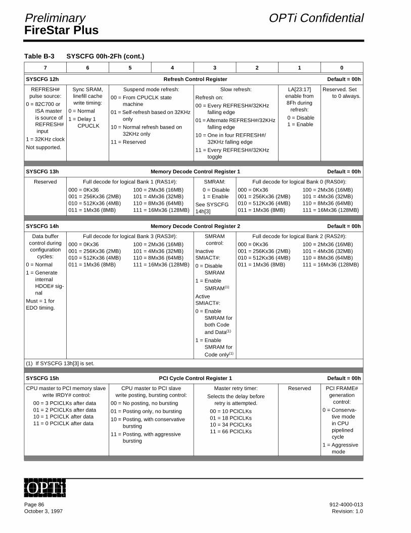
FireStar PlusPreliminary OPTi Confidential
SYSCFG 12h Refresh Control Register Default = 00h
REFRESH# pulse source:
0 = 82C700 or ISA master is source of REFRESH# input
1 = 32KHz clock
Not supported.
Sync SRAM, linefill cache write timing:
0 = Normal
1 = Delay 1 CPUCLK
Suspend mode refresh:
00 = From CPUCLK state machine
01 = Self-refresh based on 32KHz only
10 = Normal refresh based on 32KHz only
11 = Reserved
Slow refresh:
Refresh on:
00 = Every REFRESH#/32KHz falling edge
01 = Alternate REFRESH#/32KHz falling edge
10 = One in four REFRESH#/32KHz falling edge
11 = Every REFRESH#/32KHz toggle
LA[23:17] enable from 8Fh during
refresh:
0 = Disable1 = Enable
Reserved. Set to 0 always.
SYSCFG 13h Memory Decode Control Register 1 Default = 00h
Reserved Full decode for logical Bank 1 (RAS1#):
000 = 0Kx36 100 = 2Mx36 (16MB)001 = 256Kx36 (2MB) 101 = 4Mx36 (32MB)010 = 512Kx36 (4MB) 110 = 8Mx36 (64MB)011 = 1Mx36 (8MB) 111 = 16Mx36 (128MB)
SMRAM:
0 = Disable1 = Enable
See SYSCFG 14h[3]
Full decode for logical Bank 0 (RAS0#):
000 = 0Kx36 100 = 2Mx36 (16MB)001 = 256Kx36 (2MB) 101 = 4Mx36 (32MB)010 = 512Kx36 (4MB) 110 = 8Mx36 (64MB)011 = 1Mx36 (8MB) 111 = 16Mx36 (128MB)
SYSCFG 14h Memory Decode Control Register 2 Default = 00h
Data buffer control during configuration
cycles:
0 = Normal
1 = Generate internal HDOE# sig-nal
Must = 1 for EDO timing.
Full decode for logical Bank 3 (RAS3#):
000 = 0Kx36 100 = 2Mx36 (16MB)001 = 256Kx36 (2MB) 101 = 4Mx36 (32MB)010 = 512Kx36 (4MB) 110 = 8Mx36 (64MB)011 = 1Mx36 (8MB) 111 = 16Mx36 (128MB)
SMRAM control:
Inactive SMIACT#:
0 = Disable SMRAM
1 = Enable SMRAM(1)
Active SMIACT#:
0 = Enable SMRAM for both Code and Data(1)
1 = Enable SMRAM for Code only(1)
Full decode for logical Bank 2 (RAS2#):
000 = 0Kx36 100 = 2Mx36 (16MB)001 = 256Kx36 (2MB) 101 = 4Mx36 (32MB)010 = 512Kx36 (4MB) 110 = 8Mx36 (64MB)011 = 1Mx36 (8MB) 111 = 16Mx36 (128MB)
(1) If SYSCFG 13h[3] is set.
SYSCFG 15h PCI Cycle Control Register 1 Default = 00h
CPU master to PCI memory slave write IRDY# control:
00 = 3 PCICLKs after data01 = 2 PCICLKs after data10 = 1 PCICLK after data11 = 0 PCICLK after data
CPU master to PCI slave write posting, bursting control:
00 = No posting, no bursting
01 = Posting only, no bursting
10 = Posting, with conservative bursting
11 = Posting, with aggressive bursting
Master retry timer:
Selects the delay before retry is attempted.
00 = 10 PCICLKs01 = 18 PCICLKs10 = 34 PCICLKs11 = 66 PCICLKs
Reserved PCI FRAME# generation
control:
0 = Conserva-tive mode in CPU pipelined cycle
1 = Aggressive mode
Table B-3 SYSCFG 00h-2Fh (cont.)
7 6 5 4 3 2 1 0
Page 86 912-4000-013October 3, 1997 Revision: 1.0
OPTi®

FireStar PlusOPTi Confidential Preliminary
SYSCFG 16h Dirty/Tag RAM Control Register Default = A0h
This bit along with bit 5 and PCICLK3 strap define DIRTY, CMD# as PCICLK3 on the CMD# pin, and CACS# or DIRTY options on the CACS# pin.(1)
Reserved Tag RAM size selection:
0 = 8-bit
1 = 7-bit (Default)
Selects CACS# for 7-bit and DIRTY for 8-bit tag(1)
Single write hit leadoff cycle in
a combined Dirty/Tag imple-
mentation
0 = 5 cycles1 = 4 cycles
Pre-snoop control:
0 = Pre-snoop for starting address 0 only
1 = Pre-snoop for all addresses except those on the line bound-ary
Synchroniza-tion between PCICLK and
CPUCLK:
0 = PCICLK async to CPUCLK
1 = PCICLK sync to CPUCLK (skew not to exceed –2ns to 15ns)
Reserved Internal HDOE# timing control:
0 = Negated normally
1 = Negated one clock before the cycle fin-ishes
(1) ROMCS#:KBDCS# strapped for CMD#:Bits 7 & 5 CACS# Pin CMD# Pin
00 CACS# DIRTY01 CACS# DIRTY10 DIRTY CMD#11 CACS# CMD#
(1) ROMCS#:KBDCS# strapped for PCICLK3:Bits 7 & 5 CACS# Pin CMD# Pin
00 DIRTY PCICLK301 CACS# PCICLK310 DIRTY PCICLK311 CACS# PCICLK3
SYSCFG 17h PCI Cycle Control Register 2 Default = 00h
Reserved Generate NA# for PCI slave
access in async PCICLK
mode:
0 = No1 = Yes
Reserved. Set tto 0.
Reserved Reserved. Set to 0
Sync SRAM type (if
SYSCFG 11h[3] = 1):
0 = Standard1 = Pipelined
Burst type:
0 = Intel burst protocol
1 = Cyrix linear burst protocol
SYSCFG 18h Interface Control Register Default = 00h
BOFF# genera-tion for retry
cycles:
0 = BOFF# generated whenever a retry indication is asserted
1 = BOFF# asserted only if a retry is gener-ated during a Master access.
This bit should be set to 1
Drive strength on RAS lines:
0 = 16mA1 = 4mA
CAS lines volt-age selection:
0 = 5.0V1 = 3.3V
Drive strength on memory
address lines:
0 = 4mA1 = 16mA
Drive strength on write enable
line:
0 = 16mA1 = 20mA
Reserved Reserved Suspend mode Refresh fix:
0 = Disable fix
1 = Enable fix
Table B-3 SYSCFG 00h-2Fh (cont.)
7 6 5 4 3 2 1 0
912-4000-013 Page 87Revision: 1.0 October 3, 1997
OPTi®
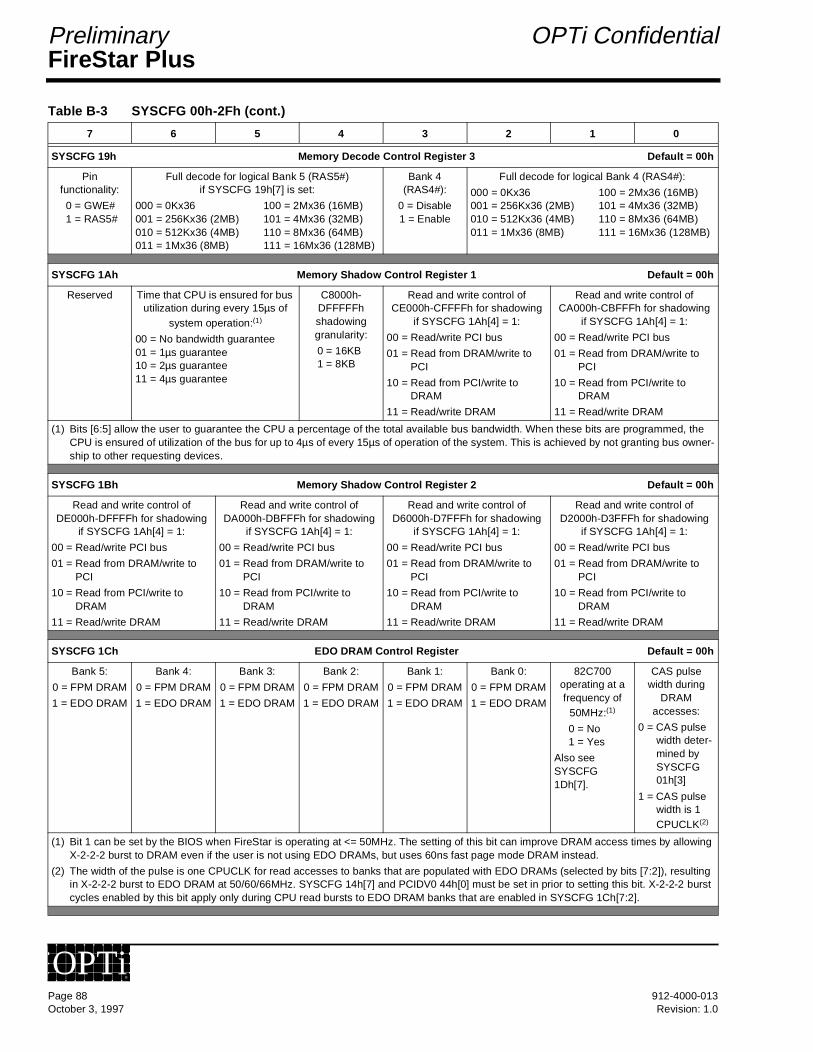
FireStar PlusPreliminary OPTi Confidential
SYSCFG 19h Memory Decode Control Register 3 Default = 00h
Pin functionality:
0 = GWE#1 = RAS5#
Full decode for logical Bank 5 (RAS5#) if SYSCFG 19h[7] is set:
000 = 0Kx36 100 = 2Mx36 (16MB)001 = 256Kx36 (2MB) 101 = 4Mx36 (32MB)010 = 512Kx36 (4MB) 110 = 8Mx36 (64MB)011 = 1Mx36 (8MB) 111 = 16Mx36 (128MB)
Bank 4(RAS4#):
0 = Disable1 = Enable
Full decode for logical Bank 4 (RAS4#):
000 = 0Kx36 100 = 2Mx36 (16MB)001 = 256Kx36 (2MB) 101 = 4Mx36 (32MB)010 = 512Kx36 (4MB) 110 = 8Mx36 (64MB)011 = 1Mx36 (8MB) 111 = 16Mx36 (128MB)
SYSCFG 1Ah Memory Shadow Control Register 1 Default = 00h
Reserved Time that CPU is ensured for bus utilization during every 15µs of
system operation:(1)
00 = No bandwidth guarantee01 = 1µs guarantee10 = 2µs guarantee11 = 4µs guarantee
C8000h-DFFFFFh shadowing granularity:
0 = 16KB1 = 8KB
Read and write control of CE000h-CFFFFh for shadowing
if SYSCFG 1Ah[4] = 1:
00 = Read/write PCI bus
01 = Read from DRAM/write to PCI
10 = Read from PCI/write to DRAM
11 = Read/write DRAM
Read and write control ofCA000h-CBFFFh for shadowing
if SYSCFG 1Ah[4] = 1:
00 = Read/write PCI bus
01 = Read from DRAM/write to PCI
10 = Read from PCI/write to DRAM
11 = Read/write DRAM
(1) Bits [6:5] allow the user to guarantee the CPU a percentage of the total available bus bandwidth. When these bits are programmed, the CPU is ensured of utilization of the bus for up to 4µs of every 15µs of operation of the system. This is achieved by not granting bus owner-ship to other requesting devices.
SYSCFG 1Bh Memory Shadow Control Register 2 Default = 00h
Read and write control of DE000h-DFFFFh for shadowing
if SYSCFG 1Ah[4] = 1:
00 = Read/write PCI bus
01 = Read from DRAM/write to PCI
10 = Read from PCI/write to DRAM
11 = Read/write DRAM
Read and write control ofDA000h-DBFFFh for shadowing
if SYSCFG 1Ah[4] = 1:
00 = Read/write PCI bus
01 = Read from DRAM/write to PCI
10 = Read from PCI/write to DRAM
11 = Read/write DRAM
Read and write control of D6000h-D7FFFh for shadowing
if SYSCFG 1Ah[4] = 1:
00 = Read/write PCI bus
01 = Read from DRAM/write to PCI
10 = Read from PCI/write to DRAM
11 = Read/write DRAM
Read and write control of D2000h-D3FFFh for shadowing
if SYSCFG 1Ah[4] = 1:
00 = Read/write PCI bus
01 = Read from DRAM/write to PCI
10 = Read from PCI/write to DRAM
11 = Read/write DRAM
SYSCFG 1Ch EDO DRAM Control Register Default = 00h
Bank 5:
0 = FPM DRAM
1 = EDO DRAM
Bank 4:
0 = FPM DRAM
1 = EDO DRAM
Bank 3:
0 = FPM DRAM
1 = EDO DRAM
Bank 2:
0 = FPM DRAM
1 = EDO DRAM
Bank 1:
0 = FPM DRAM
1 = EDO DRAM
Bank 0:
0 = FPM DRAM
1 = EDO DRAM
82C700 operating at a frequency of
50MHz:(1)
0 = No1 = Yes
Also see SYSCFG 1Dh[7].
CAS pulse width during
DRAM accesses:
0 = CAS pulse width deter-mined by SYSCFG 01h[3]
1 = CAS pulse width is 1 CPUCLK(2)
(1) Bit 1 can be set by the BIOS when FireStar is operating at <= 50MHz. The setting of this bit can improve DRAM access times by allowing X-2-2-2 burst to DRAM even if the user is not using EDO DRAMs, but uses 60ns fast page mode DRAM instead.
(2) The width of the pulse is one CPUCLK for read accesses to banks that are populated with EDO DRAMs (selected by bits [7:2]), resulting in X-2-2-2 burst to EDO DRAM at 50/60/66MHz. SYSCFG 14h[7] and PCIDV0 44h[0] must be set in prior to setting this bit. X-2-2-2 burst cycles enabled by this bit apply only during CPU read bursts to EDO DRAM banks that are enabled in SYSCFG 1Ch[7:2].
Table B-3 SYSCFG 00h-2Fh (cont.)
7 6 5 4 3 2 1 0
Page 88 912-4000-013October 3, 1997 Revision: 1.0
OPTi®
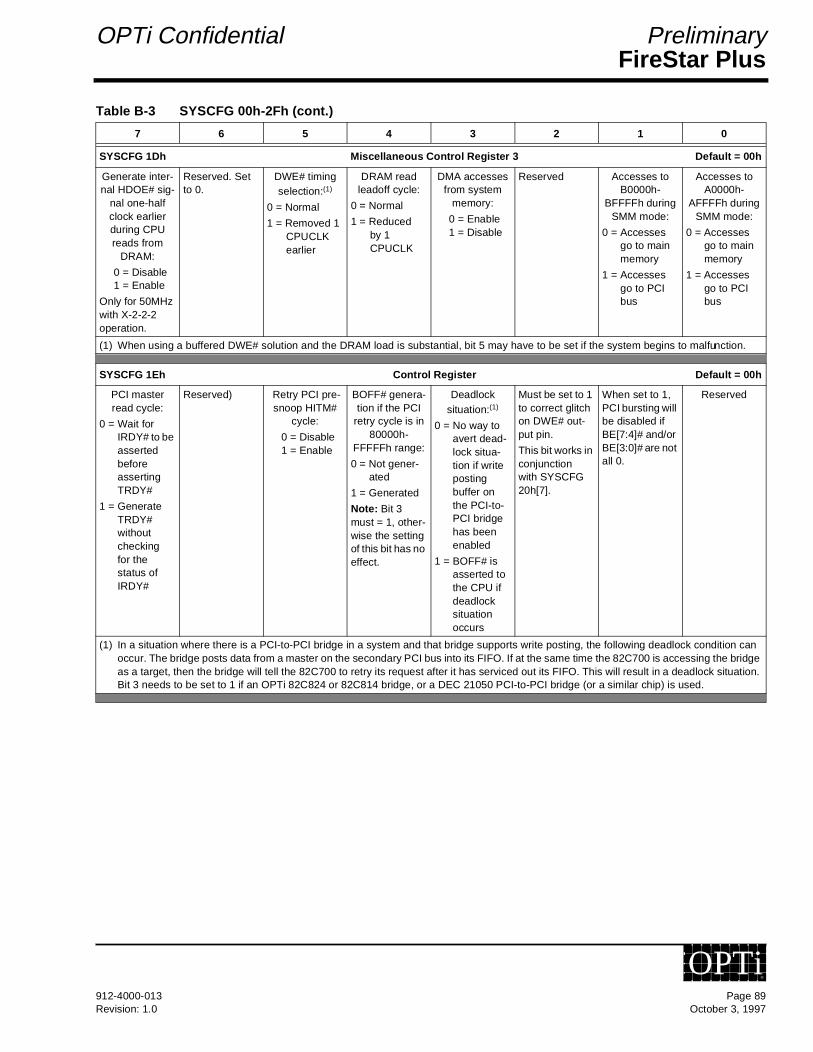
FireStar PlusOPTi Confidential Preliminary
SYSCFG 1Dh Miscellaneous Control Register 3 Default = 00h
Generate inter-nal HDOE# sig-
nal one-half clock earlier during CPU reads from
DRAM:
0 = Disable1 = Enable
Only for 50MHz with X-2-2-2 operation.
Reserved. Set to 0.
DWE# timing selection:(1)
0 = Normal
1 = Removed 1 CPUCLK earlier
DRAM read leadoff cycle:
0 = Normal
1 = Reduced by 1 CPUCLK
DMA accesses from system
memory:
0 = Enable1 = Disable
Reserved Accesses to B0000h-
BFFFFh during SMM mode:
0 = Accesses go to main memory
1 = Accesses go to PCI bus
Accesses to A0000h-
AFFFFh during SMM mode:
0 = Accesses go to main memory
1 = Accesses go to PCI bus
(1) When using a buffered DWE# solution and the DRAM load is substantial, bit 5 may have to be set if the system begins to malfunction.
SYSCFG 1Eh Control Register Default = 00h
PCI master read cycle:
0 = Wait for IRDY# to be asserted before asserting TRDY#
1 = Generate TRDY# without checking for the status of IRDY#
Reserved) Retry PCI pre-snoop HITM#
cycle:
0 = Disable1 = Enable
BOFF# genera-tion if the PCI
retry cycle is in 80000h-
FFFFFh range:
0 = Not gener-ated
1 = Generated
Note: Bit 3 must = 1, other-wise the setting of this bit has no effect.
Deadlock situation:(1)
0 = No way to avert dead-lock situa-tion if write posting buffer on the PCI-to-PCI bridge has been enabled
1 = BOFF# is asserted to the CPU if deadlock situation occurs
Must be set to 1 to correct glitch on DWE# out-put pin.
This bit works in conjunction with SYSCFG 20h[7].
When set to 1, PCI bursting will be disabled if BE[7:4]# and/or BE[3:0]# are not all 0.
Reserved
(1) In a situation where there is a PCI-to-PCI bridge in a system and that bridge supports write posting, the following deadlock condition can occur. The bridge posts data from a master on the secondary PCI bus into its FIFO. If at the same time the 82C700 is accessing the bridge as a target, then the bridge will tell the 82C700 to retry its request after it has serviced out its FIFO. This will result in a deadlock situation. Bit 3 needs to be set to 1 if an OPTi 82C824 or 82C814 bridge, or a DEC 21050 PCI-to-PCI bridge (or a similar chip) is used.
Table B-3 SYSCFG 00h-2Fh (cont.)
7 6 5 4 3 2 1 0
912-4000-013 Page 89Revision: 1.0 October 3, 1997
OPTi®
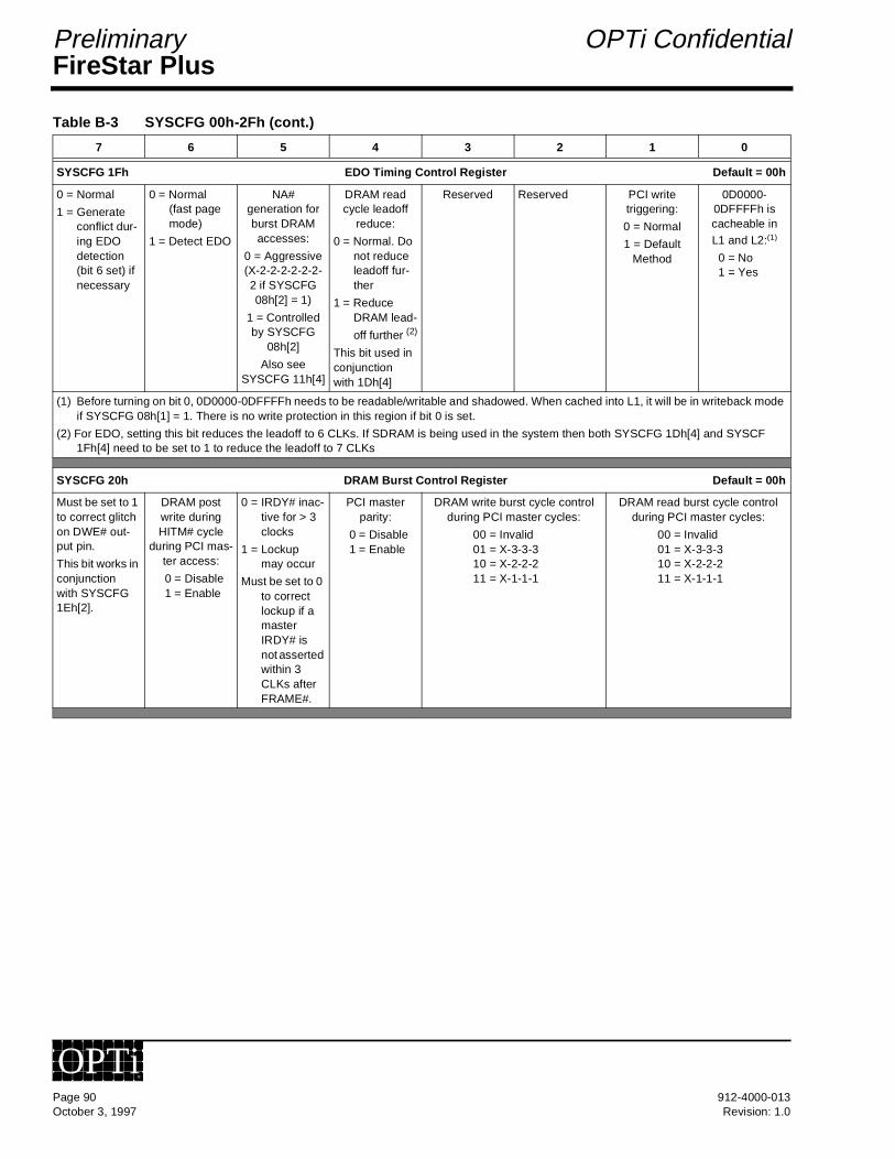
FireStar PlusPreliminary OPTi Confidential
SYSCFG 1Fh EDO Timing Control Register Default = 00h
0 = Normal
1 = Generate conflict dur-ing EDO detection (bit 6 set) if necessary
0 = Normal (fast page mode)
1 = Detect EDO
NA# generation for burst DRAM accesses:
0 = Aggressive (X-2-2-2-2-2-2-2 if SYSCFG 08h[2] = 1)
1 = Controlled by SYSCFG
08h[2]
Also see SYSCFG 11h[4]
DRAM read cycle leadoff
reduce:
0 = Normal. Do not reduce leadoff fur-ther
1 = Reduce DRAM lead-
off further (2)
This bit used in conjunction with 1Dh[4]
Reserved Reserved PCI write triggering:
0 = Normal
1 = Default Method
0D0000-0DFFFFh is cacheable in L1 and L2:(1)
0 = No1 = Yes
(1) Before turning on bit 0, 0D0000-0DFFFFh needs to be readable/writable and shadowed. When cached into L1, it will be in writeback mode if SYSCFG 08h[1] = 1. There is no write protection in this region if bit 0 is set.
(2) For EDO, setting this bit reduces the leadoff to 6 CLKs. If SDRAM is being used in the system then both SYSCFG 1Dh[4] and SYSCF 1Fh[4] need to be set to 1 to reduce the leadoff to 7 CLKs
SYSCFG 20h DRAM Burst Control Register Default = 00h
Must be set to 1 to correct glitch on DWE# out-put pin.
This bit works in conjunction with SYSCFG 1Eh[2].
DRAM post write during HITM# cycle
during PCI mas-ter access:
0 = Disable1 = Enable
0 = IRDY# inac-tive for > 3 clocks
1 = Lockup may occur
Must be set to 0 to correct lockup if a master IRDY# is not asserted within 3 CLKs after FRAME#.
PCI master parity:
0 = Disable1 = Enable
DRAM write burst cycle control during PCI master cycles:
00 = Invalid01 = X-3-3-310 = X-2-2-211 = X-1-1-1
DRAM read burst cycle control during PCI master cycles:
00 = Invalid01 = X-3-3-310 = X-2-2-211 = X-1-1-1
Table B-3 SYSCFG 00h-2Fh (cont.)
7 6 5 4 3 2 1 0
Page 90 912-4000-013October 3, 1997 Revision: 1.0
OPTi®
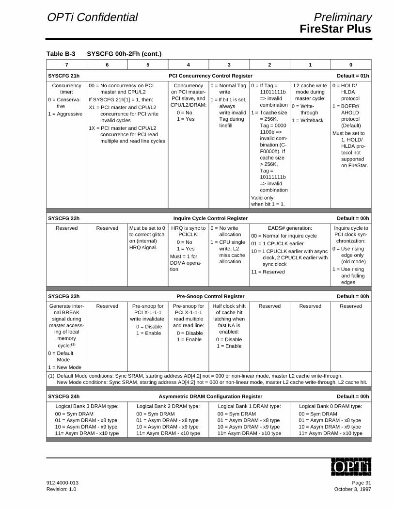
FireStar PlusOPTi Confidential Preliminary
SYSCFG 21h PCI Concurrency Control Register Default = 01h
Concurrency timer:
0 = Conserva-tive
1 = Aggressive
00 = No concurrency on PCI master and CPU/L2
If SYSCFG 21h[1] = 1, then:
X1 = PCI master and CPU/L2 concurrence for PCI write invalid cycles
1X = PCI master and CPU/L2 concurrence for PCI read multiple and read line cycles
Concurrency on PCI master-PCI slave, and CPU/L2/DRAM:
0 = No1 = Yes
0 = Normal Tag write
1 = If bit 1 is set, always write invalid Tag during linefill
0 = If Tag = 11011111b => invalid combination
1 = If cache size = 256K, Tag = 0000 1100b => invalid com-bination (C-F0000h). If cache size > 256K, Tag = 10111111b => invalid combination
Valid only when bit 1 = 1.
L2 cache write mode during master cycle:
0 = Write-through
1 = Writeback
0 = HOLD/HLDA protocol
1 = BOFF#/AHOLD protocol (Default)
Must be set to 1. HOLD/HLDA pro-tocol not supported on FireStar.
SYSCFG 22h Inquire Cycle Control Register Default = 00h
Reserved Reserved Must be set to 0 to correct glitch on (internal) HRQ signal.
HRQ is sync to PCICLK:
0 = No1 = Yes
Must = 1 for DDMA opera-tion
0 = No write allocation
1 = CPU single write, L2 miss cache allocation
EADS# generation:
00 = Normal for inquire cycle
01 = 1 CPUCLK earlier
10 = 1 CPUCLK earlier with async clock, 2 CPUCLK earlier with sync clock
11 = Reserved
Inquire cycle to PCI clock syn-chronization:
0 = Use rising edge only (old mode)
1 = Use rising and falling edges
SYSCFG 23h Pre-Snoop Control Register Default = 00h
Generate inter-nal BREAK
signal during master access-
ing of local memory cycle:(1)
0 = Default Mode
1 = New Mode
Reserved Pre-snoop for PCI X-1-1-1
write invalidate:
0 = Disable1 = Enable
Pre-snoop for PCI X-1-1-1 read multiple and read line:
0 = Disable1 = Enable
Half clock shift of cache hit
latching when fast NA is enabled:
0 = Disable1 = Enable
Reserved Reserved Reserved
(1) Default Mode conditions: Sync SRAM, starting address AD[4:2] not = 000 or non-linear mode, master L2 cache write-through.New Mode conditions: Sync SRAM, starting address AD[4:2] not = 000 or non-linear mode, master L2 cache write-through, L2 cache hit.
SYSCFG 24h Asymmetric DRAM Configuration Register Default = 00h
Logical Bank 3 DRAM type:
00 = Sym DRAM01 = Asym DRAM - x8 type10 = Asym DRAM - x9 type11= Asym DRAM - x10 type
Logical Bank 2 DRAM type:
00 = Sym DRAM01 = Asym DRAM - x8 type10 = Asym DRAM - x9 type11= Asym DRAM - x10 type
Logical Bank 1 DRAM type:
00 = Sym DRAM01 = Asym DRAM - x8 type10 = Asym DRAM - x9 type11= Asym DRAM - x10 type
Logical Bank 0 DRAM type:
00 = Sym DRAM01 = Asym DRAM - x8 type10 = Asym DRAM - x9 type11= Asym DRAM - x10 type
Table B-3 SYSCFG 00h-2Fh (cont.)
7 6 5 4 3 2 1 0
912-4000-013 Page 91Revision: 1.0 October 3, 1997
OPTi®
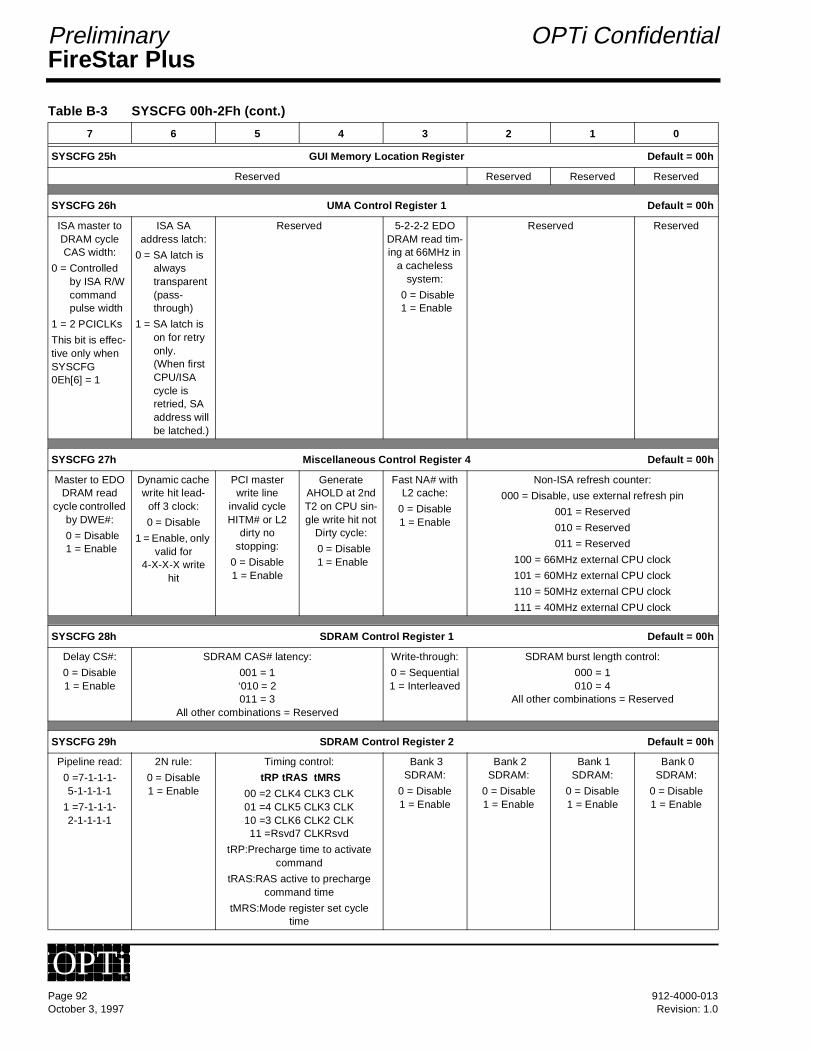
FireStar PlusPreliminary OPTi Confidential
SYSCFG 25h GUI Memory Location Register Default = 00h
Reserved Reserved Reserved Reserved
SYSCFG 26h UMA Control Register 1 Default = 00h
ISA master to DRAM cycle CAS width:
0 = Controlled by ISA R/W command pulse width
1 = 2 PCICLKs
This bit is effec-tive only when SYSCFG 0Eh[6] = 1
ISA SA address latch:
0 = SA latch is always transparent (pass-through)
1 = SA latch is on for retry only. (When first CPU/ISA cycle is retried, SA address will be latched.)
Reserved 5-2-2-2 EDO DRAM read tim-ing at 66MHz in
a cacheless system:
0 = Disable1 = Enable
Reserved Reserved
SYSCFG 27h Miscellaneous Control Register 4 Default = 00h
Master to EDO DRAM read
cycle controlled by DWE#:
0 = Disable1 = Enable
Dynamic cache write hit lead-
off 3 clock:
0 = Disable
1 = Enable, only valid for
4-X-X-X write hit
PCI master write line
invalid cycle HITM# or L2
dirty no stopping:
0 = Disable1 = Enable
Generate AHOLD at 2nd T2 on CPU sin-gle write hit not
Dirty cycle:
0 = Disable1 = Enable
Fast NA# with L2 cache:
0 = Disable1 = Enable
Non-ISA refresh counter:
000 = Disable, use external refresh pin
001 = Reserved
010 = Reserved
011 = Reserved
100 = 66MHz external CPU clock
101 = 60MHz external CPU clock
110 = 50MHz external CPU clock
111 = 40MHz external CPU clock
SYSCFG 28h SDRAM Control Register 1 Default = 00h
Delay CS#:
0 = Disable1 = Enable
SDRAM CAS# latency:
001 = 1‘010 = 2011 = 3
All other combinations = Reserved
Write-through:
0 = Sequential1 = Interleaved
SDRAM burst length control:
000 = 1010 = 4
All other combinations = Reserved
SYSCFG 29h SDRAM Control Register 2 Default = 00h
Pipeline read:
0 =7-1-1-1-5-1-1-1-1
1 =7-1-1-1-2-1-1-1-1
2N rule:
0 = Disable1 = Enable
Timing control:
tRP tRAS tMRS
00 =2 CLK4 CLK3 CLK01 =4 CLK5 CLK3 CLK10 =3 CLK6 CLK2 CLK11 =Rsvd7 CLKRsvd
tRP:Precharge time to activate command
tRAS:RAS active to precharge command time
tMRS:Mode register set cycle time
Bank 3 SDRAM:
0 = Disable1 = Enable
Bank 2 SDRAM:
0 = Disable1 = Enable
Bank 1 SDRAM:
0 = Disable1 = Enable
Bank 0 SDRAM:
0 = Disable1 = Enable
Table B-3 SYSCFG 00h-2Fh (cont.)
7 6 5 4 3 2 1 0
Page 92 912-4000-013October 3, 1997 Revision: 1.0
OPTi®

FireStar PlusOPTi Confidential Preliminary
SYSCFG 2Ah PCI-to-DRAM Control Register 1 Default = 00h
Reserved. Reserved PCI TRDY# wait state
control with PCI-to-DRAM deep buffer:
0 = 0WS (X-1-1-1)
1 = 1WS (X-2-2-2)
Write burst with PCI-to-DRAM deep buffer:
0 = Disable1 = Enable
Read burst with PCI-to-DRAM deep buffer:
0 = Disable1 = Enable
Reserved PCI-to-DRAM deep buffer
size:
0 = 16 dword1 = 24 dword
SYSCFG 2Bh PCI-to-DRAM Control Register 2 Default = 00h
Reserved Reserved
SYSCFG 2Ch CPU-to-DRAM Buffer Control Register Default = 00h
CPU-to-PCI read and CPU-to-DRAM write concurrency:
0 = Disable1 = Enable
Reserved. When set (to 1) along with CPU-to-DRAM buffer and PBSRAM, the DRAM con-troller will first supply the data to the CPU before writing the previous data back to DRAM during a cache miss dirty cycle.(1)
CPU-to-PCI write and CPU-to-DRAM read concurrency:
0 = Disable1 = Enable
Enable internal LMEM# during special cycles:
0 = No1 = Yes
BOFF# asser-tion during DRAM read
cycles:
0 = Disable1 = Enable
Data merging when CPU
owns DRAM bus:
0 = Possible only when GUI owns DRAM bus (UMA fea-ture - not supported)
1 = Always possible
Allow data collection while CPU-to-DRAM
FIFO is flushing:
0 = Disable(2)
1 = Enable
(1) Bit 5’s function needs the CPU-to-DRAM buffer to be enabled. DRAM processing for the read will start concurrently while data from cache will be written to the CPU-to-DRAM buffer.
(2) BOFF# is generated for the next DRAM write cycle as long as there is data in the FIFO.
SYSCFG 2Dh Miscellaneous Control Register 5 Default = 00h
Reserved
Table B-3 SYSCFG 00h-2Fh (cont.)
7 6 5 4 3 2 1 0
912-4000-013 Page 93Revision: 1.0 October 3, 1997
OPTi®
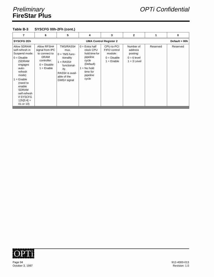
FireStar PlusPreliminary OPTi Confidential
SYSCFG 2Eh UMA Control Register 2 Default = 00h
Allow SDRAM self-refresh in Suspend mode:
0 = Disable (SDRAM engages auto-refresh mode)
1 = Enable (need to enable SDRAM self-refresh if SYSCFG 12h[5:4] = 01 or 10)
Allow RFSH# signal from IPC to connect to
DRAM controller:
0 = Disable1 = Enable
TMS/RAS5# mux.
0 = TMS func-tionality
1 = RAS5# functional-ity.
RAS5# is avail-able of the GWE# signal
0 = Extra half clock CPU hold time for pipeline cycle (Default)
1 = No hold time for pipeline cycle
CPU-to-PCI FIFO control
module:
0 = Disable1 = Enable
Number of address posting:
0 = 6 level1 = 3 Level
Reserved Reserved
Table B-3 SYSCFG 00h-2Fh (cont.)
7 6 5 4 3 2 1 0
Page 94 912-4000-013October 3, 1997 Revision: 1.0
OPTi®
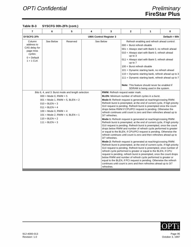
FireStar PlusOPTi Confidential Preliminary
SYSCFG 2Fh UMA Control Register 3 Default = 00h
Column address to
CAS delay for page miss
cycles:
0 = Default1 = 1 CLK
See Below Reserved See Below Refresh enabling and refresh ahead control:
000 = Burst refresh disable
001 = Always start with Bank 0, no refresh ahead
010 = Always start with Bank 0, refresh ahead up to 3
011 = Always start with Bank 0, refresh ahead up to 7
100 = Burst refresh disable
101 = Dynamic starting bank, no refresh ahead
110 = Dynamic starting bank, refresh ahead up to 3
111 = Dynamic starting bank, refresh ahead up to 7
Note: This feature should never be enabled if SDRAM is being used in the system.
Bits 6, 4, and 3: Burst mode and length selection
000 = Mode 0, RWM = 5
001 = Mode 1, RWM = 5, BLEN = 2
010 = BLEN = 3
011 = BLEN = 4
100 = Mode 0, RWM = 4
101 = Mode 2, RWM = 4, BLEN = 1
110 = BLEN = 2
111 = BLEN = 3
RWM: Refresh request water mark.
BLEN: Minimum number of refresh cycles in a burst.
Mode 0: Refresh request is generated at reaching/crossing RWM. Refresh burst is preempted, at the end of current cycle, if high priority GUI request is pending. Refresh burst is preempted once the count drops below RWM if CPU/PCI request is pending. Otherwise the refresh continues until count is zero and then refreshes ahead up to 3/7 refreshes.
Mode 1: Refresh request is generated at reaching/crossing RWM. Refresh burst is preempted, at the end of current cycle, if high priority GUI request is pending. Refresh burst is preempted, once the count drops below RWM and number of refresh cycle performed is greater or equal to the BLEN, if CPU/PCI request is pending. Otherwise the refresh continues until count is zero and then refreshes ahead up to 3/7 refreshes.
Mode 2: Refresh request is generated at reaching/crossing RWM. Refresh burst is preempted, at the end of current cycle, if high priority GUI request is pending. Refresh burst is preempted, once number of refresh cycle performed is greater or equal to the BLEN, if CPU request is pending. refresh burst is preempted, once the count drops below RWM and number of refresh cycle performed is greater or equal to the BLEN, if PCI request is pending. Otherwise the refresh continues until count is zero and then refreshes ahead up to 3/7 refreshes.
Table B-3 SYSCFG 00h-2Fh (cont.)
7 6 5 4 3 2 1 0
912-4000-013 Page 95Revision: 1.0 October 3, 1997
OPTi®
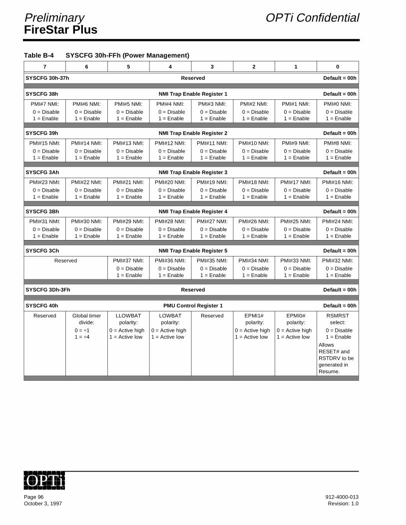
FireStar PlusPreliminary OPTi Confidential
Table B-4 SYSCFG 30h-FFh (Power Management)
7 6 5 4 3 2 1 0
SYSCFG 30h-37h Reserved Default = 00h
SYSCFG 38h NMI Trap Enable Register 1 Default = 00h
PMI#7 NMI:
0 = Disable1 = Enable
PMI#6 NMI:
0 = Disable1 = Enable
PMI#5 NMI:
0 = Disable1 = Enable
PMI#4 NMI:
0 = Disable1 = Enable
PMI#3 NMI:
0 = Disable1 = Enable
PMI#2 NMI:
0 = Disable1 = Enable
PMI#1 NMI:
0 = Disable1 = Enable
PMI#0 NMI:
0 = Disable1 = Enable
SYSCFG 39h NMI Trap Enable Register 2 Default = 00h
PMI#15 NMI:
0 = Disable1 = Enable
PMI#14 NMI:
0 = Disable1 = Enable
PMI#13 NMI:
0 = Disable1 = Enable
PMI#12 NMI:
0 = Disable1 = Enable
PMI#11 NMI:
0 = Disable1 = Enable
PMI#10 NMI:
0 = Disable1 = Enable
PMI#9 NMI:
0 = Disable1 = Enable
PMI#8 NMI:
0 = Disable1 = Enable
SYSCFG 3Ah NMI Trap Enable Register 3 Default = 00h
PMI#23 NMI:
0 = Disable1 = Enable
PMI#22 NMI:
0 = Disable1 = Enable
PMI#21 NMI:
0 = Disable1 = Enable
PMI#20 NMI:
0 = Disable1 = Enable
PMI#19 NMI:
0 = Disable1 = Enable
PMI#18 NMI:
0 = Disable1 = Enable
PMI#17 NMI:
0 = Disable1 = Enable
PMI#16 NMI:
0 = Disable1 = Enable
SYSCFG 3Bh NMI Trap Enable Register 4 Default = 00h
PMI#31 NMI:
0 = Disable1 = Enable
PMI#30 NMI:
0 = Disable1 = Enable
PMI#29 NMI:
0 = Disable1 = Enable
PMI#28 NMI:
0 = Disable1 = Enable
PMI#27 NMI:
0 = Disable1 = Enable
PMI#26 NMI:
0 = Disable1 = Enable
PMI#25 NMI:
0 = Disable1 = Enable
PMI#24 NMI:
0 = Disable1 = Enable
SYSCFG 3Ch NMI Trap Enable Register 5 Default = 00h
Reserved PMI#37 NMI:
0 = Disable1 = Enable
PMI#36 NMI:
0 = Disable1 = Enable
PMI#35 NMI:
0 = Disable1 = Enable
PMI#34 NMI:
0 = Disable1 = Enable
PMI#33 NMI:
0 = Disable1 = Enable
PMI#32 NMI:
0 = Disable1 = Enable
SYSCFG 3Dh-3Fh Reserved Default = 00h
SYSCFG 40h PMU Control Register 1 Default = 00h
Reserved Global timer divide:
0 = ÷11 = ÷4
LLOWBAT polarity:
0 = Active high1 = Active low
LOWBAT polarity:
0 = Active high1 = Active low
Reserved EPMI1# polarity:
0 = Active high1 = Active low
EPMI0# polarity:
0 = Active high1 = Active low
RSMRST select:
0 = Disable1 = Enable
Allows RESET# and RSTDRV to be generated in Resume.
Page 96 912-4000-013October 3, 1997 Revision: 1.0
OPTi®
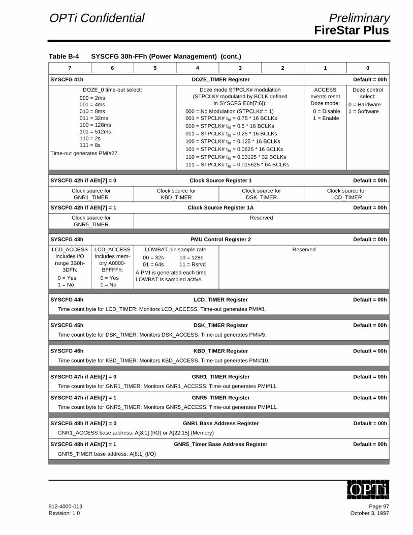
FireStar PlusOPTi Confidential Preliminary
SYSCFG 41h DOZE_TIMER Register Default = 00h
DOZE_0 time-out select:
000 = 2ms001 = 4ms010 = 8ms011 = 32ms100 = 128ms101 = 512ms110 = 2s111 = 8s
Time-out generates PMI#27.
Doze mode STPCLK# modulation(STPCLK# modulated by BCLK defined
in SYSCFG E6h[7:6]):
000 = No Modulation (STPCLK# = 1)001 = STPCLK# thi = 0.75 * 16 BCLKs
010 = STPCLK# thi = 0.5 * 16 BCLKs011 = STPCLK# thi = 0.25 * 16 BCLKs
100 = STPCLK# thi = 0.125 * 16 BCLKs
101 = STPCLK# thi = 0.0625 * 16 BCLKs
110 = STPCLK# thi = 0.03125 * 32 BCLKs111 = STPCLK# thi = 0.015625 * 64 BCLKs
ACCESS events reset Doze mode:
0 = Disable1 = Enable
Doze control select:
0 = Hardware1 = Software
SYSCFG 42h if AEh[7] = 0 Clock Source Register 1 Default = 00h
Clock source for GNR1_TIMER
Clock source for KBD_TIMER
Clock source for DSK_TIMER
Clock source for LCD_TIMER
SYSCFG 42h if AEh[7] = 1 Clock Source Register 1A Default = 00h
Clock source for GNR5_TIMER
Reserved
SYSCFG 43h PMU Control Register 2 Default = 00h
LCD_ACCESS includes I/O range 3B0h-
3DFh:
0 = Yes1 = No
LCD_ACCESS includes mem-
ory A0000-BFFFFh:
0 = Yes1 = No
LOWBAT pin sample rate:
00 = 32s 10 = 128s01 = 64s 11 = Rsrvd
A PMI is generated each time LOWBAT is sampled active.
Reserved
SYSCFG 44h LCD_TIMER Register Default = 00h
Time count byte for LCD_TIMER: Monitors LCD_ACCESS. Time-out generates PMI#8.
SYSCFG 45h DSK_TIMER Register Default = 00h
Time count byte for DSK_TIMER: Monitors DSK_ACCESS. Time-out generates PMI#9.
SYSCFG 46h KBD_TIMER Register Default = 00h
Time count byte for KBD_TIMER: Monitors KBD_ACCESS. Time-out generates PMI#10.
SYSCFG 47h if AEh[7] = 0 GNR1_TIMER Register Default = 00h
Time count byte for GNR1_TIMER: Monitors GNR1_ACCESS. Time-out generates PMI#11.
SYSCFG 47h if AEh[7] = 1 GNR5_TIMER Register Default = 00h
Time count byte for GNR5_TIMER: Monitors GNR5_ACCESS. Time-out generates PMI#11.
SYSCFG 48h if AEh[7] = 0 GNR1 Base Address Register Default = 00h
GNR1_ACCESS base address: A[8:1] (I/O) or A[22:15] (Memory)
SYSCFG 48h if AEh[7] = 1 GNR5_Timer Base Address Register Default = 00h
GNR5_TIMER base address: A[8:1] (I/O)
Table B-4 SYSCFG 30h-FFh (Power Management) (cont.)
7 6 5 4 3 2 1 0
912-4000-013 Page 97Revision: 1.0 October 3, 1997
OPTi®
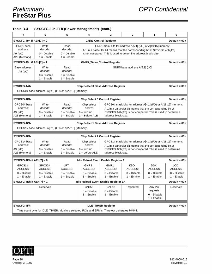
FireStar PlusPreliminary OPTi Confidential
SYSCFG 49h if AEh[7] = 0 GNR1 Control Register Default = 00h
GNR1 base address:
A9 (I/O)A23 (Memory)
Write decode:
0 = Disable1 = Enable
Read decode:
0 = Disable1 = Enable
GNR1 mask bits for address A[5:1] (I/O) or A[19:15] memory:
A 1 in a particular bit means that the corresponding bit at SYSCFG 48h[4:0] is not compared. This is used to determine address block size.
SYSCFG 49h if AEh[7] = 1 GNR5_Timer Control Register Default = 00h
Base address:
A9 (I/O)
Write decode:
0 = Disable1 = Enable
Read decode:
0 = Disable1 = Enable
GNR5 base address A[5:1] (I/O)
SYSCFG 4Ah Chip Select 0 Base Address Register Default = 00h
GPCS0# base address: A[8:1] (I/O) or A[22:15] (Memory)
SYSCFG 4Bh Chip Select 0 Control Register Default = 00h
GPCS0# base address:
A9 (I/O)A23 (Memory)
Write decode:
0 = Disable1 = Enable
Read decode:
0 = Disable1 = Enable
Chip select active:
0 = w/Cmd1 = Before ALE
GPCS0# mask bits for address A[4:1] (I/O) or A[18:15] memory:
A 1 in a particular bit means that the corresponding bit at SYSCFG 4Ah[3:0] is not compared. This is used to determineaddress block size.
SYSCFG 4Ch Chip Select 1 Base Address Register Default = 00h
GPCS1# base address: A[8:1] (I/O) or A[22:15] (Memory)
SYSCFG 4Dh Chip Select 1 Control Register Default = 00h
GPCS1# base address:
A9 (I/O)A23 (Memory)
Write decode:
0 = Disable1 = Enable
Read decode:
0 = Disable1 = Enable
Chip select active:
0 = w/Cmd1 = before ALE
GPCS1# mask bits for address A[4:1] (I/O) or A[18:15] memory:
A 1 in a particular bit means that the corresponding bit at SYSCFG 4Ch[3:0] is not compared. This is used to determineaddress block size.
SYSCFG 4Eh if AEh[7] = 0 Idle Reload Event Enable Register 1 Default = 00h
GPCS1#_ACCESS:
0 = Disable1 = Enable
GPCS0#_ACCESS:
0 = Disable1 = Enable
LPT_ACCESS:
0 = Disable1 = Enable
GNR3_ACCESS:
0 = Disable1 = Enable
GNR1_ACCESS:
0 = Disable1 = Enable
KBD_ACCESS:
0 = Disable1 = Enable
DSK_ACCESS:
0 = Disable1 = Enable
LCD_ACCESS:
0 = Disable1 = Enable
SYSCFG 4Eh if AEh[7] = 1 Idle Reload Event Enable Register 1A Default = 00h
Reserved GNR7:
0 = Disable1 = Enable
GNR5:
0 = Disable1 = Enable
Reserved Any PCI requests:
0 = Disable1 = Enable
Reserved
SYSCFG 4Fh IDLE_TIMER Register Default = 00h
Time count byte for IDLE_TIMER: Monitors selected IRQs and EPMIs. Time-out generates PMI#4.
Table B-4 SYSCFG 30h-FFh (Power Management) (cont.)
7 6 5 4 3 2 1 0
Page 98 912-4000-013October 3, 1997 Revision: 1.0
OPTi®

FireStar PlusOPTi Confidential Preliminary
SYSCFG 50h PMU Control Register 3 Default = 00h
Software start SMI:
0 = Clear SMI1 = Start SMI
Reserved IRQ8 polarity:
0 = Active low1 = Active high
14.3MHz to 82C700:
0 = Enable1 = Disable
Write = 1 to start Doze
Read = Doze status:
0 = Counting1 = Timed out
Ready to Resume (RO):
0 = Not in Resume
1 = Ready to Resume
PMU mode (RO):
0 = Nothing pending
1 = Suspend active (clear PMI#6)
Start Suspend(WO):
1 = Enter Suspend mode
SYSCFG 51h Beeper Control Register Default = 00h
Reserved Beeper control:
00 = No Action01 = 1kHz10 = Off11 = 2kHz
SYSCFG 52h Scratchpad Register 1 Default = 00h
General purpose storage byte:
- For CISA Configuration Cycles: Data phase information, low byte
SYSCFG 53h Scratchpad Register 2 Default = 00h
General purpose storage byte.
- For CISA Configuration Cycles: Data phase information, high byte
SYSCFG 54h Power Control Latch Register 1 Default = 00h
Enable [3:0] to write latch lines PPWR[3:0]:
0 = Disable1 = Enable
Read/write data bits for PPWR[3:0]:
0 = Latch output low1 = Latch output high
SYSCFG 55h Power Control Latch Register 2 Default = 0Fh
Enable [3:0] to write latch lines PPWR[7:4]:
0 = Disable1 = Enable
Read/write data bits for PPWR[7:4] (Default = 1111):
0 = Latch output low1 = Latch output high
SYSCFG 56h Reserved Default = 00h
SYSCFG 57h PMU Control Register 4 Default = 08h
Reserved INTRGRP gen-erates PMI#6:
0 = Disable1 = Enable
DSK_ACCESSincludes FDD:
0 = Yes1 = No
DSK_ACCESSincludes HDD:
0 = Yes1 = No
LCD video area includes A and B segments:
0 = Disable1 = Enable
LCD video frame buffer
area, use PCIDV0
41h[7:0] and 40h[7:6]:
0 = Disable1 = Enable
Reserved
Table B-4 SYSCFG 30h-FFh (Power Management) (cont.)
7 6 5 4 3 2 1 0
912-4000-013 Page 99Revision: 1.0 October 3, 1997
OPTi®

FireStar PlusPreliminary OPTi Confidential
SYSCFG 58h PMU Event Register 1 Default = 00h
LOWBAT PMI#3 SMI:
00 = Disable11 = Enable
EPMI1# PMI#2 SMI:
00 = Disable11 = Enable
EPMI0# PMI#1 SMI:
00 = Disable11 = Enable
LLOWBAT PMI#0 SMI:
00 = Disable11 = Enable
SYSCFG 59h PMU Event Register 2 Default = 00h
Allow software SMI:
0 = Disable1 = Enable
Reload timers on Resume:
0 = No1 = Yes
Resume INTRGRP PMI#6, Suspend PMI#7 SMI:
00 = Disable11 = Enable
R_TIMER PMI#5 SMI:
00 = Disable11 = Enable
IDLE_TIMER PMI#4 SMI:
00 = Disable11 = Enable
SYSCFG 5Ah if AEh[7] = 0 PMU Event Register 3 Default = 00h
GNR1_TIMER PMI#11 GNR1_ACCESS PMI#15:
00 = Disable01 = Positive decode10 = Positive decode, SMI11 = SMI
KBD_TIMER PMI#10KBD_ACCESS PMI#14:
00 = Disable01 = Positive decode10 = Positive decode, SMI11 = SMI
DSK_TIMER PMI#9DSK_ACCESS PMI#13:
00 = Disable01 = Positive decode10 = Positive decode, SMI11 = SMI
LCD_TIMER PMI#8LCD_ACCESS PMI#12:
00 = Disable01 = Reserved10 = Reserved11 = SMI
SYSCFG 5Ah if AEh[7] = 1 PMU Event Register 3A Default = 00h
GNR5_TIMER PMI:
00 = Disable01 = Positive decode10 = Positive decode, SMI11 = SMI
Reserved
SYSCFG 5Bh if AEh[7] = 0 PMU Event Register 4 Default = 00h
Reserved Global SMI control:
0 = Allow1 = Mask
Reserved GNR1 Next Access
PMI#15:
0 = Disable1 = Enable
KBD Next Access
PMI#14:
0 = Disable1 = Enable
DSK Next Access
PMI#13:
0 = Disable1 = Enable
LCD Next Access
PMI#12:
0 = Disable1 = Enable
SYSCFG 5Bh if AEh[7] = 1 PMU Event Register 4A Default = 00h
Reserved GNR5 Next Access
PMI#15:
0 = Disable1 = Enable
Reserved
SYSCFG 5Ch PMI SMI Source Register 1 (Write 1 to Clear) Default = 00h
PMI#7, Suspend:
0 = Not Active1 = Active
PMI#6, Resume or INTRGRP:
0 = Not Active1 = Active
PMI#5, R_TIMER time-out:
0 = Not Active1 = Active
PMI#4, IDLE_TIMER
time-out:
0 = Not Active1 = Active
PMI#3, LOWBAT:
0 = Not Active1 = Active
PMI#2, EPMI1#:
0 = Not Active1 = Active
PMI#1, EPMI0#:
0 = Not Active1 = Active
PMI#0, LLOWBAT:
0 = Not Active1 = Active
SYSCFG 5Dh if AEh[7] = 0 PMI SMI Source Register 2 (Write 1 to Clear) Default = 00h
PMI#15, GNR1_
ACCESS:
0 = None1 = Active
PMI#14, KBD_ACCESS:
0 = Not Active1 = Active
PMI#13, DSK_ACCESS:
0 = Not Active1 = Active
PMI#12, LCD_ACCESS:
0 = Not Active1 = Active
PMI#11, GNR1_TIMER:
0 = Not Active1 = Active
PMI#10, KBD_TIMER:
0 = Not Active1= Active
PMI#9, DSK_TIMER:
0 = Not Active1 = Active
PMI#8, LCD_TIMER:
0 = Not Active1 = Active
Table B-4 SYSCFG 30h-FFh (Power Management) (cont.)
7 6 5 4 3 2 1 0
Page 100 912-4000-013October 3, 1997 Revision: 1.0
OPTi®
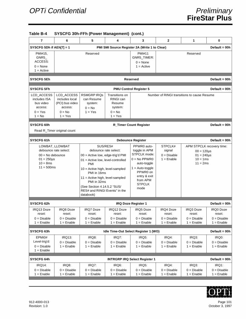
FireStar PlusOPTi Confidential Preliminary
SYSCFG 5Dh if AEh[7] = 1 PMI SMI Source Register 2A (Write 1 to Clear) Default = 00h
PMI#15, GNR5_
ACCESS:
0 = None1 = Active
Reserved PMI#11 GNR5_TIMER:
0 = None1 = Active
Reserved
SYSCFG 5Eh Reserved Default = 00h
SYSCFG 5Fh PMU Control Register 5 Default = 00h
LCD_ACCESS includes ISA
bus video access:
0 = Yes1 = No
LCD_ACCESS includes local
(PCI) bus video access:
0 = No1 = Yes
RSMGRP IRQs can Resume
system:
0 = No1 = Yes
Transitions on RINGI can Resume system:
0 = No1 = Yes
Number of RINGI transitions to cause Resume
SYSCFG 60h R_Timer Count Register Default = 00h
Read R_Timer original count
SYSCFG 61h Debounce Register Default = 00h
LOWBAT, LLOWBAT debounce rate select:
00 = No debounce01 = 250µs10 = 8ms11 = 500ms
SUS/RES#debounce rate select:
00 = Active low, edge-trig’d PMI
01 = Active low, level-controlled PMI
10 = Active high, level-sampled PMI in 16ms
11 = Active high, level-sampled PMI in 32ms
(See Section 4.14.5.2 “SUS/RES# and RINGI Events” in the databook)
PPWR0 auto-toggle in APM
STPCLK mode:
0 = No PPWR0 auto-toggle
1 = Auto-toggle PPWR0 on entry & exit from APM STPCLK mode
STPCLK# signal
0 = Disable1 = Enable
APM STPCLK recovery time:
00 = 120µs01 = 240µs10 = 1ms11 = 2ms
SYSCFG 62h IRQ Doze Register 1 Default = 00h
IRQ13 Doze reset:
0 = Disable1 = Enable
IRQ8 Doze reset:
0 = Disable1 = Enable
IRQ7 Doze reset:
0 = Disable1 = Enable
IRQ12 Doze reset:
0 = Disable1 = Enable
IRQ5 Doze reset:
0 = Disable1 = Enable
IRQ4 Doze reset:
0 = Disable1 = Enable
IRQ3 Doze reset:
0 = Disable1 = Enable
IRQ0 Doze reset:
0 = Disable1 = Enable
SYSCFG 63h Idle Time-Out Select Register 1 (WO) Default = 00h
EPMI0#Level-trig'd:
0 = Disable1 = Enable
IRQ13:
0 = Disable1 = Enable
IRQ8:
0 = Disable1 = Enable
IRQ7:
0 = Disable1 = Enable
IRQ5:
0 = Disable1 = Enable
IRQ4:
0 = Disable1 = Enable
IRQ3:
0 = Disable1 = Enable
IRQ0:
0 = Disable1 = Enable
SYSCFG 64h INTRGRP IRQ Select Register 1 Default = 00h
IRQ14:
0 = Disable1 = Enable
IRQ8:
0 = Disable1 = Enable
IRQ7:
0 = Disable1 = Enable
IRQ6:
0 = Disable1 = Enable
IRQ5:
0 = Disable1 = Enable
IRQ4:
0 = Disable1 = Enable
IRQ3:
0 = Disable1 = Enable
IRQ1:
0 = Disable1 = Enable
Table B-4 SYSCFG 30h-FFh (Power Management) (cont.)
7 6 5 4 3 2 1 0
912-4000-013 Page 101Revision: 1.0 October 3, 1997
OPTi®
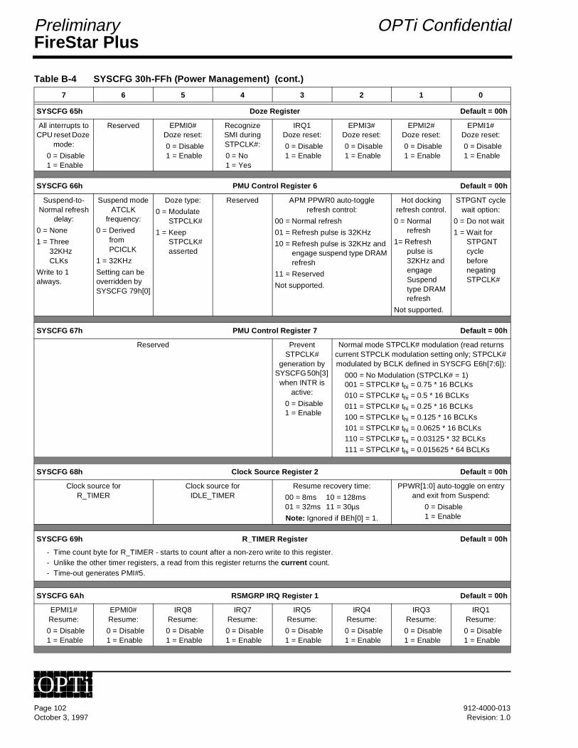
FireStar PlusPreliminary OPTi Confidential
SYSCFG 65h Doze Register Default = 00h
All interrupts to CPU reset Doze
mode:
0 = Disable1 = Enable
Reserved EPMI0# Doze reset:
0 = Disable1 = Enable
Recognize SMI during STPCLK#:
0 = No1 = Yes
IRQ1 Doze reset:
0 = Disable1 = Enable
EPMI3# Doze reset:
0 = Disable1 = Enable
EPMI2# Doze reset:
0 = Disable1 = Enable
EPMI1# Doze reset:
0 = Disable1 = Enable
SYSCFG 66h PMU Control Register 6 Default = 00h
Suspend-to-Normal refresh
delay:
0 = None
1 = Three 32KHz CLKs
Write to 1 always.
Suspend mode ATCLK
frequency:
0 = Derived from PCICLK
1 = 32KHz
Setting can be overridden by SYSCFG 79h[0]
Doze type:
0 = Modulate STPCLK#
1 = Keep STPCLK# asserted
Reserved APM PPWR0 auto-toggle refresh control:
00 = Normal refresh
01 = Refresh pulse is 32KHz
10 = Refresh pulse is 32KHz and engage suspend type DRAM refresh
11 = Reserved
Not supported.
Hot docking refresh control.
0 = Normal refresh
1= Refresh pulse is 32KHz and engage Suspend type DRAM refresh
Not supported.
STPGNT cycle wait option:
0 = Do not wait
1 = Wait for STPGNT cycle before negating STPCLK#
SYSCFG 67h PMU Control Register 7 Default = 00h
Reserved Prevent STPCLK#
generation by SYSCFG 50h[3]
when INTR is active:
0 = Disable1 = Enable
Normal mode STPCLK# modulation (read returns current STPCLK modulation setting only; STPCLK# modulated by BCLK defined in SYSCFG E6h[7:6]):
000 = No Modulation (STPCLK# = 1)001 = STPCLK# thi = 0.75 * 16 BCLKs
010 = STPCLK# thi = 0.5 * 16 BCLKs
011 = STPCLK# thi = 0.25 * 16 BCLKs
100 = STPCLK# thi = 0.125 * 16 BCLKs
101 = STPCLK# thi = 0.0625 * 16 BCLKs110 = STPCLK# thi = 0.03125 * 32 BCLKs
111 = STPCLK# thi = 0.015625 * 64 BCLKs
SYSCFG 68h Clock Source Register 2 Default = 00h
Clock source forR_TIMER
Clock source forIDLE_TIMER
Resume recovery time:
00 = 8ms 10 = 128ms01 = 32ms 11 = 30µs
Note: Ignored if BEh[0] = 1.
PPWR[1:0] auto-toggle on entry and exit from Suspend:
0 = Disable1 = Enable
SYSCFG 69h R_TIMER Register Default = 00h
- Time count byte for R_TIMER - starts to count after a non-zero write to this register. - Unlike the other timer registers, a read from this register returns the current count. - Time-out generates PMI#5.
SYSCFG 6Ah RSMGRP IRQ Register 1 Default = 00h
EPMI1# Resume:
0 = Disable1 = Enable
EPMI0# Resume:
0 = Disable1 = Enable
IRQ8Resume:
0 = Disable1 = Enable
IRQ7Resume:
0 = Disable1 = Enable
IRQ5Resume:
0 = Disable1 = Enable
IRQ4Resume:
0 = Disable1 = Enable
IRQ3Resume:
0 = Disable1 = Enable
IRQ1Resume:
0 = Disable1 = Enable
Table B-4 SYSCFG 30h-FFh (Power Management) (cont.)
7 6 5 4 3 2 1 0
Page 102 912-4000-013October 3, 1997 Revision: 1.0
OPTi®

FireStar PlusOPTi Confidential Preliminary
SYSCFG 6Bh Resume Source Register Default = 00h
DRAM Suspend mode refresh
type:
0 = Slow refresh (normal)
1 = Self-refresh
PREQ# caused Resume (RO):
0 = No1 = Yes
CLKRUN# caused
Resume (RO):
0 = No1 = Yes
Reserved:
Write as read.
CISA SEL#/ATB# low caused
Resume (RO):
0 = No1 = Yes
SUSP/RSM caused
Resume (RO):
0 = No1 = Yes
RSMGRP caused
Resume (RO):
0 = No1 = Yes
RI caused Resume (RO):
0 = No1 = Yes
SYSCFG 6Ch Scratchpad Register 3 Default = 00h
General purpose storage byte
- For CISA Configuration Cycles: Address phase 1 information, low byte
SYSCFG 6Dh Scratchpad Register 4 Default = 00h
General purpose storage byte
- For CISA Configuration Cycles: Address phase 1 information, high byte
SYSCFG 6Eh Scratchpad Register 5 Default = 00h
General purpose storage byte
- For CISA Configuration Cycles: Address phase 2 information, low byte
SYSCFG 6Fh Scratchpad Register 6 Default = 00h
General purpose storage byte
- For CISA Configuration Cycles: Address phase 2 information, high byte
SYSCFG 70h GNR1 Base Address Register 1 Default = 00h
GNR1_ACCESS base address: A[13:6] for memory watchdog or A[15:10] for I/O (right-aligned).
SYSCFG 71h GNR1 Control Register 1 Default = FFh
GNR1_ACCESS mask bits: Mask for A[13:6] for memory watchdog or mask for A[15:10] for I/O (right-aligned).
SYSCFG 72h GNR1 Control Register 2 Default = 00h
GNR1_ACCESS base address: A[5:2] for memory watchdog or ignored for I/O.
GNR1_ACCESS mask bits: Mask for A[5:2] for memory watchdog or mask for A[9:6] for I/O.
SYSCFG 73h GNR2 Base Address Register 1 Default = 00h
GNR2_ACCESS base address: A[13:6] for memory watchdog or A[15:10] for I/O (right-aligned).
SYSCFG 74h GNR2 Control Register 1 Default = FFh
GNR2_ACCESS mask bits: Mask for A[13:6] for memory watchdog or mask for A[15:10] for I/O (right-aligned).
SYSCFG 75h GNR2 Control Register 2 Default = 00h
GNR2_ACCESS base address:A[5:2] for memory watchdog or ignored for I/O.
GNR2_ACCESS mask bits:Mask for A[5:2] for memory watchdog or mask for A[9:6] for I/O.
Table B-4 SYSCFG 30h-FFh (Power Management) (cont.)
7 6 5 4 3 2 1 0
912-4000-013 Page 103Revision: 1.0 October 3, 1997
OPTi®

FireStar PlusPreliminary OPTi Confidential
SYSCFG 76h if AEh[7] = 0 Doze Reload Select Register 1 Default = 0Fh
LCD_ACCESS:
0 = DOZE_01 = DOZE_1
KBD_ACCESS:
0 = DOZE_01 = DOZE_1
DSK_ACCESS:
0 = DOZE_01 = DOZE_1
HDU_ACCESS:
0 = DOZE_01 = DOZE_1
COM1&2_ACCESS:
0 = DOZE_01 = DOZE_1
LPT_ACCESS:
0 = DOZE_01 = DOZE_1
GNR1_ACCESS:
0 = DOZE_01 = DOZE_1
GNR2_ACCESS:
0 = DOZE_01 = DOZE_1
SYSCFG 76h if AEh[7] = 1 Doze Reload Select Register 1A Default = 03h
Reserved PREQ#:
0 = DOZE_01 = DOZE_1
CLKRUN#:
0 = DOZE_01 = DOZE_1
Reserved GNR5:
0 = DOZE_01 = DOZE_1
GNR6:
0 = DOZE_01 = DOZE_1
SYSCFG 77h Doze Reload Select Register 2 Default = 00h
IRQ8:
0 = DOZE_01 = DOZE_1
IRQ7:
0 = DOZE_01 = DOZE_1
IRQ6:
0 = DOZE_01 = DOZE_1
IRQ5:
0 = DOZE_01 = DOZE_1
IRQ4:
0 = DOZE_01 = DOZE_1
IRQ3:
0 = DOZE_01 = DOZE_1
IRQ1:
0 = DOZE_01 = DOZE_1
IRQ0:
0 = DOZE_01 = DOZE_1
SYSCFG 78h Doze Reload Select Register 3 Default = 00h
PCI:
0 = DOZE_01 = DOZE_1
IRQ15:
0 = DOZE_01 = DOZE_1
IRQ14:
0 = DOZE_01 = DOZE_1
IRQ13:
0 = DOZE_01 = DOZE_1
IRQ12:
0 = DOZE_01 = DOZE_1
IRQ11:
0 = DOZE_01 = DOZE_1
IRQ10:
0 = DOZE_01 = DOZE_1
IRQ9:
0 = DOZE_01 = DOZE_1
SYSCFG 79h PMU Control Register 8 Default = 00h
DOZE_1 time-out select:
000 = No delay (Default) 100 = 64ms 001 = 1ms 101 = 256ms 010 = 4ms 110 = 1s
011 = 16ms 111 = 4s
PMI# event trig-gers exit from Doze mode if
the PMI event is enabled to gen-
erate SMI:(1)
0 = No1 = Yes
Reserved PREQ# wake up Suspend:
0 = Disable1 = Enable
CLKRUN# wake up Suspend:
0 = Disable1 = Enable
ATCLK during Suspend:
0 = Run
1 = Stopped (overrides SYSCFG 66h[6])
(1) For example, to let PMI#11 reset the Doze mode without generating SMI to the CPU, SYSCFG 5Ah[7:6] must = 11 and SYSCFG 5Bh[6] must = 1.
SYSCFG 7Ah GNR3 Base Address Register 1 Default = 00h
GNR3_ACCESS base address: A[13:6] for memory watchdog or A[15:10] for I/O (right-aligned).
SYSCFG 7Bh GNR3 Control Register 1 Default = FFh
GNR3_ACCESS mask bits: Mask for A[13:6] for memory watchdog or mask for A[15:10] for I/O (right-aligned).
SYSCFG 7Ch GNR3 Control Register 2 Default = 00h
GNR3_ACCESS base address:A[5:2] for memory watchdog or ignored for I/O.
GNR3_ACCESS mask bits:Mask for A[5:2] for memory watchdog or mask for A[9:6] for I/O.
SYSCFG 7Dh GNR4 Base Address Register 1 Default = 00h
GNR4_ACCESS base address: A[13:6] for memory watchdog or A[15:10] for I/O (right-aligned).
SYSCFG 7Eh GNR4 Control Register 1 Default = FFh
GNR4_ACCESS mask bits: Mask for A[13:6] for memory watchdog or mask for A[15:10] for I/O (right-aligned).
Table B-4 SYSCFG 30h-FFh (Power Management) (cont.)
7 6 5 4 3 2 1 0
Page 104 912-4000-013October 3, 1997 Revision: 1.0
OPTi®
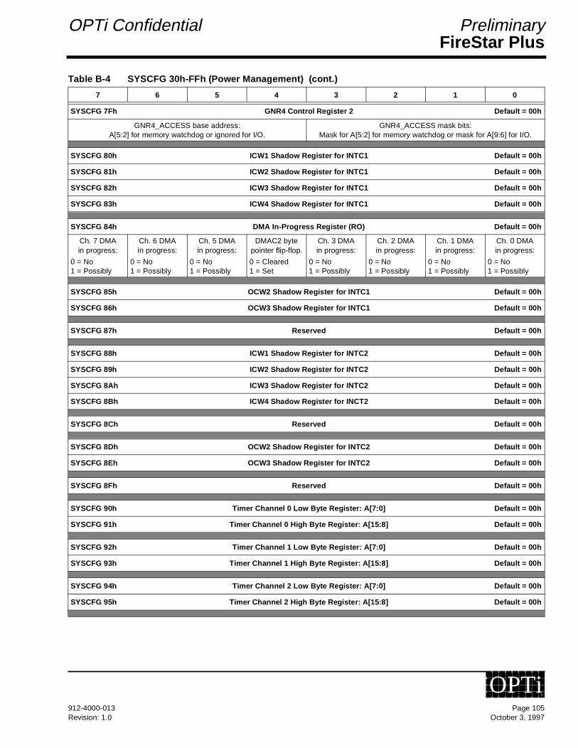
FireStar PlusOPTi Confidential Preliminary
SYSCFG 7Fh GNR4 Control Register 2 Default = 00h
GNR4_ACCESS base address:A[5:2] for memory watchdog or ignored for I/O.
GNR4_ACCESS mask bits:Mask for A[5:2] for memory watchdog or mask for A[9:6] for I/O.
SYSCFG 80h ICW1 Shadow Register for INTC1 Default = 00h
SYSCFG 81h ICW2 Shadow Register for INTC1 Default = 00h
SYSCFG 82h ICW3 Shadow Register for INTC1 Default = 00h
SYSCFG 83h ICW4 Shadow Register for INTC1 Default = 00h
SYSCFG 84h DMA In-Progress Register (RO) Default = 00h
Ch. 7 DMA in progress:
0 = No1 = Possibly
Ch. 6 DMA in progress:
0 = No1 = Possibly
Ch. 5 DMA in progress:
0 = No1 = Possibly
DMAC2 byte pointer flip-flop.
0 = Cleared1 = Set
Ch. 3 DMA in progress:
0 = No1 = Possibly
Ch. 2 DMA in progress:
0 = No1 = Possibly
Ch. 1 DMA in progress:
0 = No1 = Possibly
Ch. 0 DMA in progress:
0 = No1 = Possibly
SYSCFG 85h OCW2 Shadow Register for INTC1 Default = 00h
SYSCFG 86h OCW3 Shadow Register for INTC1 Default = 00h
SYSCFG 87h Reserved Default = 00h
SYSCFG 88h ICW1 Shadow Register for INTC2 Default = 00h
SYSCFG 89h ICW2 Shadow Register for INTC2 Default = 00h
SYSCFG 8Ah ICW3 Shadow Register for INTC2 Default = 00h
SYSCFG 8Bh ICW4 Shadow Register for INCT2 Default = 00h
SYSCFG 8Ch Reserved Default = 00h
SYSCFG 8Dh OCW2 Shadow Register for INTC2 Default = 00h
SYSCFG 8Eh OCW3 Shadow Register for INTC2 Default = 00h
SYSCFG 8Fh Reserved Default = 00h
SYSCFG 90h Timer Channel 0 Low Byte Register: A[7:0] Default = 00h
SYSCFG 91h Timer Channel 0 High Byte Register: A[15:8] Default = 00h
SYSCFG 92h Timer Channel 1 Low Byte Register: A[7:0] Default = 00h
SYSCFG 93h Timer Channel 1 High Byte Register: A[15:8] Default = 00h
SYSCFG 94h Timer Channel 2 Low Byte Register: A[7:0] Default = 00h
SYSCFG 95h Timer Channel 2 High Byte Register: A[15:8] Default = 00h
Table B-4 SYSCFG 30h-FFh (Power Management) (cont.)
7 6 5 4 3 2 1 0
912-4000-013 Page 105Revision: 1.0 October 3, 1997
OPTi®
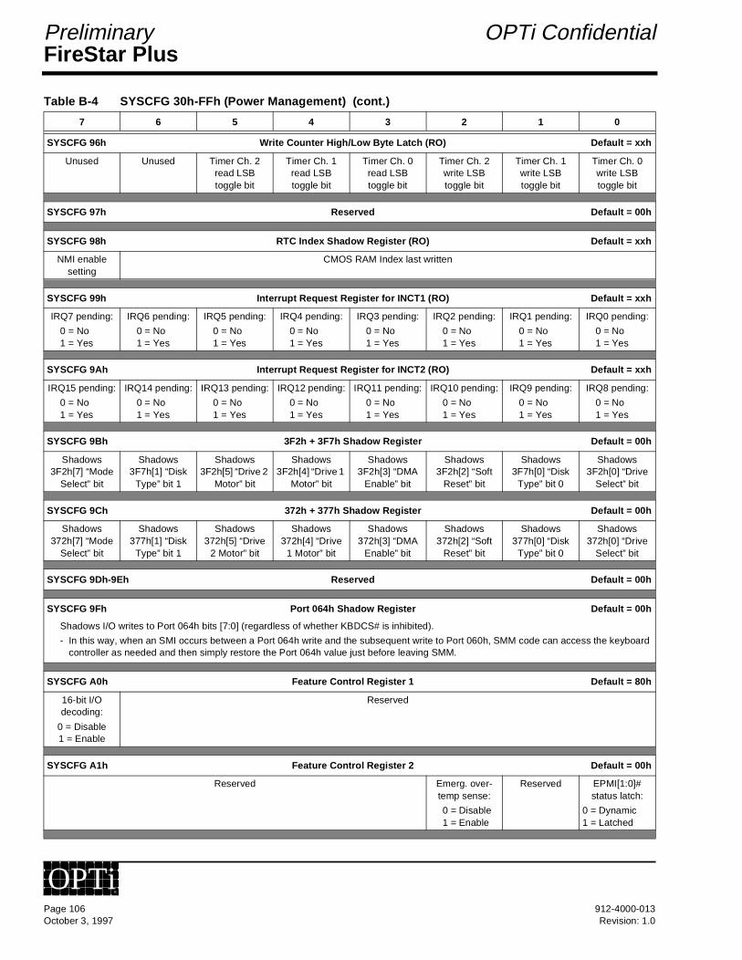
FireStar PlusPreliminary OPTi Confidential
SYSCFG 96h Write Counter High/Low Byte Latch (RO) Default = xxh
Unused Unused Timer Ch. 2 read LSB toggle bit
Timer Ch. 1 read LSB toggle bit
Timer Ch. 0 read LSB toggle bit
Timer Ch. 2 write LSB toggle bit
Timer Ch. 1 write LSB toggle bit
Timer Ch. 0 write LSB toggle bit
SYSCFG 97h Reserved Default = 00h
SYSCFG 98h RTC Index Shadow Register (RO) Default = xxh
NMI enable setting
CMOS RAM Index last written
SYSCFG 99h Interrupt Request Register for INCT1 (RO) Default = xxh
IRQ7 pending:
0 = No1 = Yes
IRQ6 pending:
0 = No1 = Yes
IRQ5 pending:
0 = No1 = Yes
IRQ4 pending:
0 = No1 = Yes
IRQ3 pending:
0 = No1 = Yes
IRQ2 pending:
0 = No1 = Yes
IRQ1 pending:
0 = No1 = Yes
IRQ0 pending:
0 = No1 = Yes
SYSCFG 9Ah Interrupt Request Register for INCT2 (RO) Default = xxh
IRQ15 pending:
0 = No1 = Yes
IRQ14 pending:
0 = No1 = Yes
IRQ13 pending:
0 = No1 = Yes
IRQ12 pending:
0 = No1 = Yes
IRQ11 pending:
0 = No1 = Yes
IRQ10 pending:
0 = No1 = Yes
IRQ9 pending:
0 = No1 = Yes
IRQ8 pending:
0 = No1 = Yes
SYSCFG 9Bh 3F2h + 3F7h Shadow Register Default = 00h
Shadows 3F2h[7] “Mode
Select” bit
Shadows 3F7h[1] “Disk
Type” bit 1
Shadows 3F2h[5] “Drive 2
Motor” bit
Shadows 3F2h[4] “Drive 1
Motor” bit
Shadows 3F2h[3] “DMA
Enable” bit
Shadows 3F2h[2] “Soft
Reset” bit
Shadows 3F7h[0] “Disk
Type” bit 0
Shadows 3F2h[0] “Drive
Select” bit
SYSCFG 9Ch 372h + 377h Shadow Register Default = 00h
Shadows 372h[7] “Mode
Select” bit
Shadows 377h[1] “Disk
Type” bit 1
Shadows 372h[5] “Drive
2 Motor” bit
Shadows 372h[4] “Drive
1 Motor” bit
Shadows 372h[3] “DMA
Enable” bit
Shadows 372h[2] “Soft
Reset” bit
Shadows 377h[0] “Disk
Type” bit 0
Shadows 372h[0] “Drive
Select” bit
SYSCFG 9Dh-9Eh Reserved Default = 00h
SYSCFG 9Fh Port 064h Shadow Register Default = 00h
Shadows I/O writes to Port 064h bits [7:0] (regardless of whether KBDCS# is inhibited).
- In this way, when an SMI occurs between a Port 064h write and the subsequent write to Port 060h, SMM code can access the keyboard controller as needed and then simply restore the Port 064h value just before leaving SMM.
SYSCFG A0h Feature Control Register 1 Default = 80h
16-bit I/O decoding:
0 = Disable1 = Enable
Reserved
SYSCFG A1h Feature Control Register 2 Default = 00h
Reserved Emerg. over-temp sense:
0 = Disable1 = Enable
Reserved EPMI[1:0]#status latch:
0 = Dynamic1 = Latched
Table B-4 SYSCFG 30h-FFh (Power Management) (cont.)
7 6 5 4 3 2 1 0
Page 106 912-4000-013October 3, 1997 Revision: 1.0
OPTi®
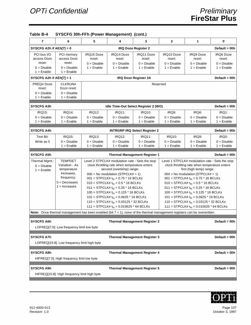
FireStar PlusOPTi Confidential Preliminary
SYSCFG A2h if AEh[7] = 0 IRQ Doze Register 2 Default = 00h
PCI bus I/O access Doze
reset:
0 = Disable1 = Enable
PCI memory access Doze
reset:
0 = Disable1 = Enable
IRQ15 Doze reset:
0 = Disable1 = Enable
IRQ14 Doze reset:
0 = Disable1 = Enable
IRQ11 Doze reset:
0 = Disable1 = Enable
IRQ10 Doze reset:
0 = Disable1 = Enable
IRQ9 Doze reset:
0 = Disable1 = Enable
IRQ6 Doze reset:
0 = Disable1 = Enable
SYSCFG A2h if AEh[7] = 1 IRQ Doze Register 2A Default = 00h
PREQ# Doze reset:
0 = Disable1 = Enable
CLKRUN# Doze reset:
0 = Disable1 = Enable
Reserved
SYSCFG A3h Idle Time-Out Select Register 2 (WO) Default = 00h
IRQ15:
0 = Disable1 = Enable
IRQ14:
0 = Disable1 = Enable
IRQ12:
0 = Disable1 = Enable
IRQ11:
0 = Disable1 = Enable
IRQ10:
0 = Disable1 = Enable
IRQ9:
0 = Disable1 = Enable
IRQ6:
0 = Disable1 = Enable
IRQ1:
0 = Disable1 = Enable
SYSCFG A4h INTRGRP IRQ Select Register 2 Default = 00h
Test Bit:
Write as 0
IRQ15:
0 = Disable1 = Enable
IRQ13:
0 = Disable1 = Enable
IRQ12:
0 = Disable1 = Enable
IRQ11:
0 = Disable1 = Enable
IRQ10:
0 = Disable1 = Enable
IRQ9:
0 = Disable1 = Enable
IRQ0:
0 = Disable1 = Enable
SYSCFG A5h Thermal Management Register 1 Default = 00h
Thermal Mgmt.:
0 = Disable1 = Enable
TEMPDET Variation - As temperature increases, frequency:
0 = Decreases1 = Increases
Level 2 STPCLK# modulation rate - Sets the stop clock throttling rate when temperature enters
second (overtemp) range:
000 = No modulation (STPCLK# = 1)001 = STPCLK# thi = 0.75 * 16 BCLKs
010 = STPCLK# thi = 0.5 * 16 BCLKs
011 = STPCLK# thi = 0.25 * 16 BCLKs100 = STPCLK# thi = 0.125 * 16 BCLKs
101 = STPCLK# thi = 0.0625 * 16 BCLKs
110 = STPCLK# thi = 0.03125 * 32 BCLKs
111 = STPCLK# thi = 0.015625 * 64 BCLKs
Level 1 STPCLK# modulation rate - Sets the stop clock throttling rate when temperature enters
first (high temp) range:
000 = No modulation (STPCLK# = 1)001 = STPCLK# thi = 0.75 * 16 BCLKs
010 = STPCLK# thi = 0.5 * 16 BCLKs
011 = STPCLK# thi = 0.25 * 16 BCLKs100 = STPCLK# thi = 0.125 * 16 BCLKs
101 = STPCLK# thi = 0.0625 * 16 BCLKs
110 = STPCLK# thi = 0.03125 * 32 BCLKs
111 = STPCLK# thi = 0.015625 * 64 BCLKs
Note: Once thermal management has been enabled (bit 7 = 1), none of the thermal management registers can be overwritten.
SYSCFG A6h Thermal Management Register 2 Default = 00h
LOFREQ[7:0]: Low frequency limit low byte
SYSCFG A7h Thermal Management Register 3 Default = 00h
LOFREQ[15:8]: Low frequency limit high byte
SYSCFG A8h Thermal Management Register 4 Default = 00h
HIFREQ[7:0]: High frequency limit low byte
SYSCFG A9h Thermal Management Register 5 Default = 00h
HIFREQ[15:8]: High frequency limit high byte
Table B-4 SYSCFG 30h-FFh (Power Management) (cont.)
7 6 5 4 3 2 1 0
912-4000-013 Page 107Revision: 1.0 October 3, 1997
OPTi®

FireStar PlusPreliminary OPTi Confidential
SYSCFG AAh Thermal Management Register 6 Default = 00h
Emergency Overtemp SensorSTPCLK# Modulation Rate:
000 = No modulation (STPCLK# = 1)001 = STPCLK# thi = 0.75 * 16 BCLKs
010 = STPCLK# thi = 0.5 * 16 BCLKs
011 = STPCLK# thi = 0.25 * 16 BCLKs100 = STPCLK# thi = 0.125 * 16 BCLKs
101 = STPCLK# thi = 0.0625 * 16 BCLKs
110 = STPCLK# thi = 0.03125 * 32 BCLKs
111 = STPCLK# thi = 0.015625 * 64 BCLKs
THMIN pin polarity:
0 = High1 = Low
EPMI trigger for thermal mgmt.
00 = EPMI0#01 = EPMI1#10 = EPMI2#11 = EPMI3#
Also see bit 1.
THMIN input:
0 = THMIN
1 = EPMI indi-cated in bits [3:2]
HDI input:
0 = HDI
1 = EPMI indi-cated by SYSCFG F0h[1:0]
SYSCFG ABh Power Control Latch Register 3 Default = 00h
Enable [3:0] to write latch lines PPWR[11:8]:
0 = Disable1 = Enable
Read/write data bits for PPWR[11:8]:
0 = Latch output low1 = Latch output high
SYSCFG ACh Dynamic Clock Control Register Default = 00h
Reserved B7 Pin Func-tion Select
0 = DCCEN
1 = MA13
Block other STPCLK#
sources when DCCEN active
0 = No
1 = Yes
Current state of DCCEN pin
(RO)
0 = Low
1 = high
STPCLK# Deassertion delay from DCCEN state change
00 = 0.5 - 0.7ms
01 = 1.0 - 1.3ms
10 = 1.7 - 2.0ms
11 = 1.00 - 1.25s
Activated/deac-tivate fre-
quency change
0 = No effect
1 = Toggle DCCEN
SYSCFG ADh Feature Control Register 3 Default = 00h
Reserved CPU power state in
Suspend:
0 = Powered1 = 0 Volt
PCIIDE responds as:
0 = Device 14h, Function 0
1 = Device 01h, Function 1
INIT operation:
0 = Normal
1 = Toggle on Resume
PCIIDE Device ID:
0 = D568h1 = D721h
Reserved
SYSCFG AEh GNR_ACCESS Feature Register 1 Default = 03h
GNR set select:
0 = GNR1-41 = GNR5-8
Reserved GNR2 cycle decode type:
0 = I/O1 = Memory
GNR1 cycle decode type:
0 = I/O1 = Memory
GNR2 base address:
A0 (I/O)A14 (Memory)
GNR1 base address:
A0 (I/O)A14 (Memory)
GNR2 mask bit:
A0 (I/O)A14 (Memory)
GNR1 mask bit:
A0 (I/O)A14 (Memory)
SYSCFG AFh-B0h Reserved Default = 00h
SYSCFG B1h RSMGRP IRQ Register 2 Default = 00h
EPMI3# Resume:
0 = Disable1 = Enable
EPMI2# Resume:
0 = Disable1 = Enable
IRQ15Resume:
0 = Disable1 = Enable
IRQ14Resume:
0 = Disable1 = Enable
IRQ12Resume:
0 = Disable1 = Enable
IRQ11Resume:
0 = Disable1 = Enable
IRQ10Resume:
0 = Disable1 = Enable
IRQ9Resume:
0 = Disable1 = Enable
SYSCFG B2h if AEh[7] = 0 Clock Source Register 3 Default = 00h
Clock source for HDU_TIMER
Clock source for COM2_TIMER
Clock source for COM1_TIMER
Clock source for GNR2_TIMER
Table B-4 SYSCFG 30h-FFh (Power Management) (cont.)
7 6 5 4 3 2 1 0
Page 108 912-4000-013October 3, 1997 Revision: 1.0
OPTi®

FireStar PlusOPTi Confidential Preliminary
SYSCFG B2h if AEh[7] = 1 Clock Source Register 3A Default = 00h
Reserved Clock source for GNR6_TIMER
SYSCFG B3h Chip Select Cycle Type Register Default = 00h
GPCS3# ROM width:
0 = 8-bit1 = 16-bit
GPCS2# ROM width:
0 = 8-bit1 = 16-bit
GPCS1# ROM width:
0 = 8-bit1 = 16-bit
GPCS0# ROM width:
0 = 8-bit1 = 16-bit
GPCS3# cycle type:
0 = I/O1 = ROMCS
GPCS2# cycle type:
0 = I/O1 = ROMCS
GPCS1# cycle type:
0 = I/O1 = ROMCS
GPCS0# cycle type:
0 = I/O1 = ROMCS
SYSCFG B4h HDU_TIMER Register Default = 00h
Time count byte for HDU_TIMER: Monitors HDU_ACCESS. Time-out generates PMI#19.
SYSCFG B5h COM1_TIMER Register Default = 00h
Time count byte for COM1_TIMER: Monitors COM1_ACCESS. Time-out generates PMI#17.
SYSCFG B6h COM2_TIMER Register Default = 00h
Time count byte for COM2_TIMER: Monitors COM2_ACCESS. Time-out generates PMI#18.
SYSCFG B7h if AEh[7] = 0 GNR2_TIMER Register Default = 00h
Time count byte for GNR2_TIMER: Monitors GNR2_ACCESS. Time-out generates PMI#16.
SYSCFG B7h if AEh[7] = 1 GNR6_TIMER Register Default = 00h
Time count byte for GNR6_TIMER: Monitors GNR6_ACCESS. Time-out generates PMI#16.
SYSCFG B8h if AEh[7] = 0 GNR2 Base Address Register Default = 00h
GNR2_ACCESS base address: A[8:1] (I/O) or A[22:15] (Memory)
SYSCFG B8h if AEh[7] = 1 GNR6 Base Address Register Default = 00h
GNR6_Timer base address: A[8:1] (I/O)
SYSCFG B9h if AEh[7] = 0 GNR2 Control Register Default = 00h
GNR2 base address:
A9 (I/O)A23 (Memory)
Write decode:
0 = Disable1 = Enable
Read decode:
0 = Disable1 = Enable
GNR2 mask bits for address A[5:1] (I/O) or A[19:15] memory:
A 1 in a particular bit means that the corresponding bit at B8h[4:0] is not compared. This is used to determine address block size.
SYSCFG B9h if AEh[7] = 1 GNR6 Control Register Default = 00h
GNR6 base address:
A9 (I/O)
Write decode:
0 = Disable1 = Enable
Read decode:
0 = Disable1 = Enable
GNR6 mask bits for address A[5:1] (I/O)
SYSCFG BAh Chip Select 2 Base Address Register Default = 00h
GPCS2# base address: A[8:1] (I/O) or A[22:15] (Memory)
Table B-4 SYSCFG 30h-FFh (Power Management) (cont.)
7 6 5 4 3 2 1 0
912-4000-013 Page 109Revision: 1.0 October 3, 1997
OPTi®
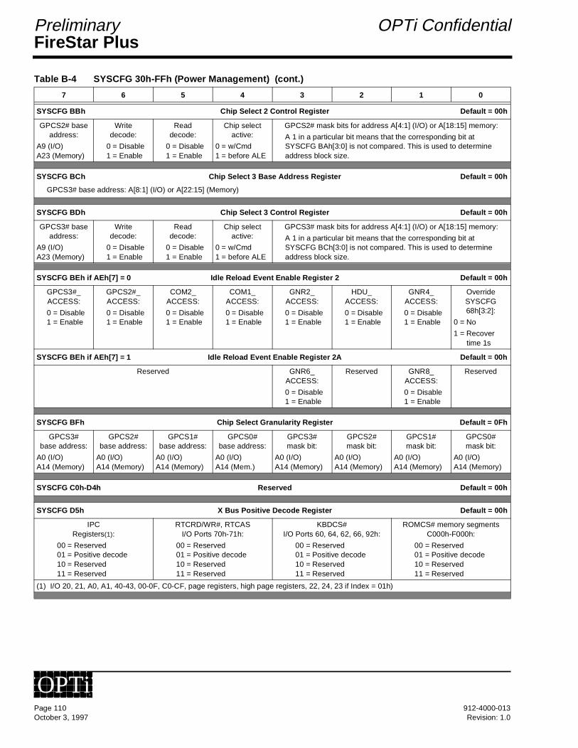
FireStar PlusPreliminary OPTi Confidential
SYSCFG BBh Chip Select 2 Control Register Default = 00h
GPCS2# base address:
A9 (I/O)A23 (Memory)
Write decode:
0 = Disable1 = Enable
Read decode:
0 = Disable1 = Enable
Chip select active:
0 = w/Cmd1 = before ALE
GPCS2# mask bits for address A[4:1] (I/O) or A[18:15] memory:
A 1 in a particular bit means that the corresponding bit at SYSCFG BAh[3:0] is not compared. This is used to determineaddress block size.
SYSCFG BCh Chip Select 3 Base Address Register Default = 00h
GPCS3# base address: A[8:1] (I/O) or A[22:15] (Memory)
SYSCFG BDh Chip Select 3 Control Register Default = 00h
GPCS3# base address:
A9 (I/O)A23 (Memory)
Write decode:
0 = Disable1 = Enable
Read decode:
0 = Disable1 = Enable
Chip select active:
0 = w/Cmd1 = before ALE
GPCS3# mask bits for address A[4:1] (I/O) or A[18:15] memory:
A 1 in a particular bit means that the corresponding bit at SYSCFG BCh[3:0] is not compared. This is used to determineaddress block size.
SYSCFG BEh if AEh[7] = 0 Idle Reload Event Enable Register 2 Default = 00h
GPCS3#_ACCESS:
0 = Disable1 = Enable
GPCS2#_ACCESS:
0 = Disable1 = Enable
COM2_ACCESS:
0 = Disable1 = Enable
COM1_ACCESS:
0 = Disable1 = Enable
GNR2_ACCESS:
0 = Disable1 = Enable
HDU_ACCESS:
0 = Disable1 = Enable
GNR4_ACCESS:
0 = Disable1 = Enable
Override SYSCFG 68h[3:2]:
0 = No
1 = Recover time 1s
SYSCFG BEh if AEh[7] = 1 Idle Reload Event Enable Register 2A Default = 00h
Reserved GNR6_ACCESS:
0 = Disable1 = Enable
Reserved GNR8_ACCESS:
0 = Disable1 = Enable
Reserved
SYSCFG BFh Chip Select Granularity Register Default = 0Fh
GPCS3# base address:
A0 (I/O)A14 (Memory)
GPCS2# base address:
A0 (I/O)A14 (Memory)
GPCS1# base address:
A0 (I/O)A14 (Memory)
GPCS0# base address:
A0 (I/O)A14 (Mem.)
GPCS3# mask bit:
A0 (I/O)A14 (Memory)
GPCS2# mask bit:
A0 (I/O)A14 (Memory)
GPCS1# mask bit:
A0 (I/O)A14 (Memory)
GPCS0# mask bit:
A0 (I/O)A14 (Memory)
SYSCFG C0h-D4h Reserved Default = 00h
SYSCFG D5h X Bus Positive Decode Register Default = 00h
IPCRegisters(1):
00 = Reserved01 = Positive decode10 = Reserved11 = Reserved
RTCRD/WR#, RTCASI/O Ports 70h-71h:
00 = Reserved01 = Positive decode10 = Reserved11 = Reserved
KBDCS#I/O Ports 60, 64, 62, 66, 92h:
00 = Reserved01 = Positive decode10 = Reserved11 = Reserved
ROMCS# memory segments C000h-F000h:
00 = Reserved01 = Positive decode10 = Reserved11 = Reserved
(1) I/O 20, 21, A0, A1, 40-43, 00-0F, C0-CF, page registers, high page registers, 22, 24, 23 if Index = 01h)
Table B-4 SYSCFG 30h-FFh (Power Management) (cont.)
7 6 5 4 3 2 1 0
Page 110 912-4000-013October 3, 1997 Revision: 1.0
OPTi®
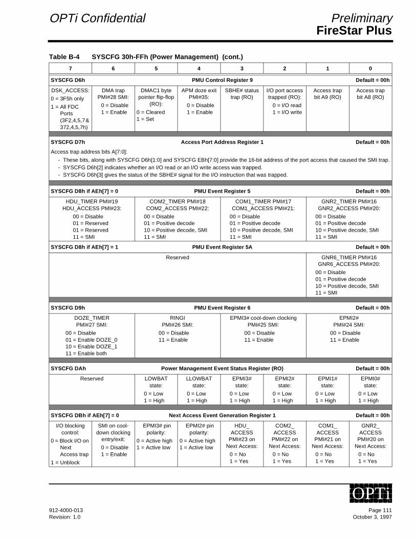
FireStar PlusOPTi Confidential Preliminary
SYSCFG D6h PMU Control Register 9 Default = 00h
DSK_ACCESS:
0 = 3F5h only
1 = All FDC Ports (3F2,4,5,7 & 372,4,5,7h)
DMA trap PMI#28 SMI:
0 = Disable1 = Enable
DMAC1 byte pointer flip-flop
(RO):
0 = Cleared1 = Set
APM doze exit PMI#35:
0 = Disable1 = Enable
SBHE# status trap (RO)
I/O port access trapped (RO):
0 = I/O read1 = I/O write
Access trapbit A9 (RO)
Access trapbit A8 (RO)
SYSCFG D7h Access Port Address Register 1 Default = 00h
Access trap address bits A[7:0]:
- These bits, along with SYSCFG D6h[1:0] and SYSCFG EBh[7:0] provide the 16-bit address of the port access that caused the SMI trap.- SYSCFG D6h[2] indicates whether an I/O read or an I/O write access was trapped. - SYSCFG D6h[3] gives the status of the SBHE# signal for the I/O instruction that was trapped.
SYSCFG D8h if AEh[7] = 0 PMU Event Register 5 Default = 00h
HDU_TIMER PMI#19HDU_ACCESS PMI#23:
00 = Disable01 = Reserved01 = Reserved11 = SMI
COM2_TIMER PMI#18COM2_ACCESS PMI#22:
00 = Disable01 = Positive decode10 = Positive decode, SMI11 = SMI
COM1_TIMER PMI#17COM1_ACCESS PMI#21:
00 = Disable01 = Positive decode10 = Positive decode, SMI11 = SMI
GNR2_TIMER PMI#16GNR2_ACCESS PMI#20:
00 = Disable01 = Positive decode10 = Positive decode, SMI11 = SMI
SYSCFG D8h if AEh[7] = 1 PMU Event Register 5A Default = 00h
Reserved GNR6_TIMER PMI#16GNR6_ACCESS PMI#20:
00 = Disable01 = Positive decode10 = Positive decode, SMI11 = SMI
SYSCFG D9h PMU Event Register 6 Default = 00h
DOZE_TIMER PMI#27 SMI:
00 = Disable01 = Enable DOZE_010 = Enable DOZE_111 = Enable both
RINGI PMI#26 SMI:
00 = Disable11 = Enable
EPMI3# cool-down clocking PMI#25 SMI:
00 = Disable11 = Enable
EPMI2# PMI#24 SMI:
00 = Disable11 = Enable
SYSCFG DAh Power Management Event Status Register (RO) Default = 00h
Reserved LOWBAT state:
0 = Low1 = High
LLOWBAT state:
0 = Low1 = High
EPMI3# state:
0 = Low1 = High
EPMI2# state:
0 = Low1 = High
EPMI1# state:
0 = Low1 = High
EPMI0# state:
0 = Low1 = High
SYSCFG DBh if AEh[7] = 0 Next Access Event Generation Register 1 Default = 00h
I/O blocking control:
0 = Block I/O on Next Access trap
1 = Unblock
SMI on cool-down clocking
entry/exit:
0 = Disable1 = Enable
EPMI3# pin polarity:
0 = Active high1 = Active low
EPMI2# pin polarity:
0 = Active high1 = Active low
HDU_ACCESS
PMI#23 on Next Access:
0 = No1 = Yes
COM2_ACCESS
PMI#22 on Next Access:
0 = No1 = Yes
COM1_ACCESS
PMI#21 on Next Access:
0 = No1 = Yes
GNR2_ACCESS
PMI#20 on Next Access:
0 = No1 = Yes
Table B-4 SYSCFG 30h-FFh (Power Management) (cont.)
7 6 5 4 3 2 1 0
912-4000-013 Page 111Revision: 1.0 October 3, 1997
OPTi®

FireStar PlusPreliminary OPTi Confidential
SYSCFG DBh if AEh[7] = 1 Next Access Event Generation Register 1A Default = 00h
Reserved GNR6_ACCESS
PMI#20 on Next Access:
0 = No1 = Yes
SYSCFG DCh if AEh[7] = 0 PMU SMI Source Register 1 (Write 1 to Clear) Default = 00h
PMI#23, HDU_
ACCESS:
0 = Inactive1 = Active
PMI#22, COM2_
ACCESS:
0 = Inactive1 = Active
PMI#21, COM1_
ACCESS:
0 = Inactive1 = Active
PMI#20, GNR2_
ACCESS:
0 = Inactive1 = Active
PMI#19, HDU_
TIMER:
0 = Inactive1 = Active
PMI#18, COM2_TIMER:
0 = Inactive1 = Active
PMI#17, COM1_TIMER:
0 = Inactive1 = Active
PMI#16, GNR2_TIMER:
0 = Inactive1 = Active
SYSCFG DCh if AEh[7] = 1 PMU SMI Source Register 1A (Write 1 to Clear) Default = 00h
Reserved PMI#20, GNR6_
ACCESS:
0 = Clear1 = Active
Reserved PMI#16, GNR6_TIMER:
0 = Clear1 = Active
SYSCFG DDh PMU SMI Source Register 2 (Write 1 to Clear) Default = 00h
PMI#39,PCI retry
limit:
0 = Inactive1 = Active
PMI#38, CISA/PCI IRQ driveback trap:
0 = Inactive1 = Active
PMI#37, DMA_
ACCESS:
0 = Inactive1 = Active
PMI#28, DMA
Request:
0 = Inactive1 = Active
PMI#27, DOZE_TIMER:
0 = Inactive1 = Active
PMI#26, RINGI:
0 = Inactive1 = Active
PMI#25, EPMI3# pin/ cool-down clocking:
0 = Inactive1 = Active
PMI#24, EPMI2#
pin:
0 = Inactive1 = Active
SYSCFG DDh - FS ACPI Version PMU SMI Source Register 2 (Write 1 to Clear) Default = 00h
PMI#39,ACPI SMI:
0 = Inactive1 = Active
PMI#38, CISA/PCI IRQ driveback trap:
0 = Inactive1 = Active
PMI#37, DMA_
ACCESS:
0 = Inactive1 = Active
PMI#28, DMA
Request:
0 = Inactive1 = Active
PMI#27, DOZE_TIMER:
0 = Inactive1 = Active
PMI#26, RINGI:
0 = Inactive1 = Active
PMI#25, EPMI3# pin/ cool-down clocking:
0 = Inactive1 = Active
PMI#24, EPMI2#
pin:
0 = Inactive1 = Active
SYSCFG DEh if AEh[7] = 0 Current Access Event Generation Register 1 Default = 00h
HDU_ACCESS
PMI#23 on Current Access:
0 = No1 = Yes
COM2_ ACCESS
PMI#22 on Current Access:
0 = No1 = Yes
COM1_ ACCESS
PMI#21 on Current Access:
0 = No1 = Yes
GNR2_ ACCESS
PMI#20 on Current Access:
0 = No1 = Yes
GNR1_ ACCESS
PMI#15 on Current Access:
0 = No1 = Yes
KBD_ACCESS
PMI#14 on Current Access:
0 = No1 = Yes
DSK_ACCESS
PMI#13 on Current Access:
0 = No1 = Yes
LCD_ACCESS
PMI#12 on Current Access:
0 = No1 = Yes
SYSCFG DEh if AEh[7] = 1 Current Access Event Generation Register 1A Default = 00h
Reserved GNR6_ ACCESS
PMI#20 on Current Access:
0 = No1 = Yes
Reserved
Table B-4 SYSCFG 30h-FFh (Power Management) (cont.)
7 6 5 4 3 2 1 0
Page 112 912-4000-013October 3, 1997 Revision: 1.0
OPTi®
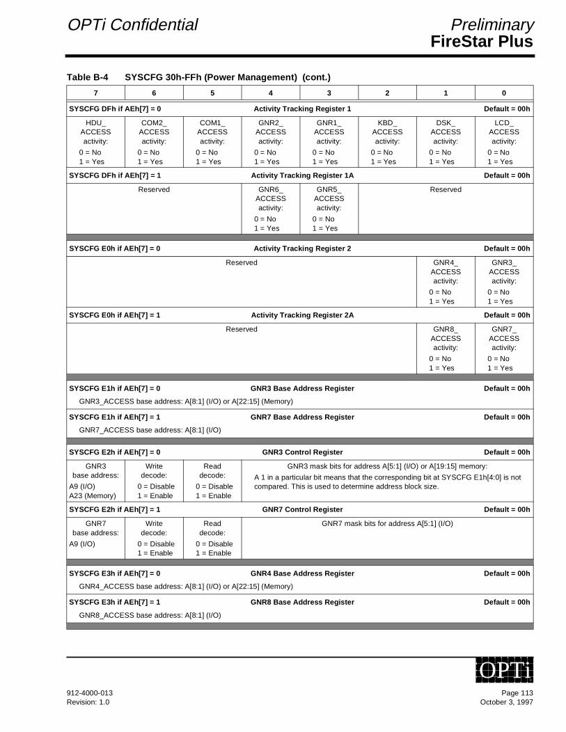
FireStar PlusOPTi Confidential Preliminary
SYSCFG DFh if AEh[7] = 0 Activity Tracking Register 1 Default = 00h
HDU_ACCESSactivity:
0 = No1 = Yes
COM2_ACCESSactivity:
0 = No1 = Yes
COM1_ACCESSactivity:
0 = No1 = Yes
GNR2_ACCESSactivity:
0 = No1 = Yes
GNR1_ACCESSactivity:
0 = No1 = Yes
KBD_ACCESSactivity:
0 = No1 = Yes
DSK_ACCESSactivity:
0 = No1 = Yes
LCD_ACCESSactivity:
0 = No1 = Yes
SYSCFG DFh if AEh[7] = 1 Activity Tracking Register 1A Default = 00h
Reserved GNR6_ACCESSactivity:
0 = No1 = Yes
GNR5_ACCESSactivity:
0 = No1 = Yes
Reserved
SYSCFG E0h if AEh[7] = 0 Activity Tracking Register 2 Default = 00h
Reserved GNR4_ACCESSactivity:
0 = No1 = Yes
GNR3_ACCESSactivity:
0 = No1 = Yes
SYSCFG E0h if AEh[7] = 1 Activity Tracking Register 2A Default = 00h
Reserved GNR8_ACCESSactivity:
0 = No1 = Yes
GNR7_ACCESSactivity:
0 = No1 = Yes
SYSCFG E1h if AEh[7] = 0 GNR3 Base Address Register Default = 00h
GNR3_ACCESS base address: A[8:1] (I/O) or A[22:15] (Memory)
SYSCFG E1h if AEh[7] = 1 GNR7 Base Address Register Default = 00h
GNR7_ACCESS base address: A[8:1] (I/O)
SYSCFG E2h if AEh[7] = 0 GNR3 Control Register Default = 00h
GNR3base address:
A9 (I/O)A23 (Memory)
Write decode:
0 = Disable1 = Enable
Read decode:
0 = Disable1 = Enable
GNR3 mask bits for address A[5:1] (I/O) or A[19:15] memory:
A 1 in a particular bit means that the corresponding bit at SYSCFG E1h[4:0] is not compared. This is used to determine address block size.
SYSCFG E2h if AEh[7] = 1 GNR7 Control Register Default = 00h
GNR7base address:
A9 (I/O)
Write decode:
0 = Disable1 = Enable
Read decode:
0 = Disable1 = Enable
GNR7 mask bits for address A[5:1] (I/O)
SYSCFG E3h if AEh[7] = 0 GNR4 Base Address Register Default = 00h
GNR4_ACCESS base address: A[8:1] (I/O) or A[22:15] (Memory)
SYSCFG E3h if AEh[7] = 1 GNR8 Base Address Register Default = 00h
GNR8_ACCESS base address: A[8:1] (I/O)
Table B-4 SYSCFG 30h-FFh (Power Management) (cont.)
7 6 5 4 3 2 1 0
912-4000-013 Page 113Revision: 1.0 October 3, 1997
OPTi®
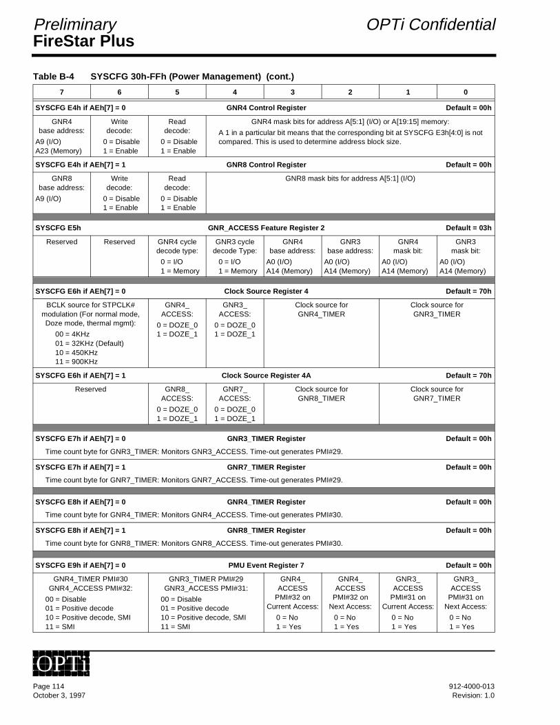
FireStar PlusPreliminary OPTi Confidential
SYSCFG E4h if AEh[7] = 0 GNR4 Control Register Default = 00h
GNR4base address:
A9 (I/O)A23 (Memory)
Write decode:
0 = Disable1 = Enable
Read decode:
0 = Disable1 = Enable
GNR4 mask bits for address A[5:1] (I/O) or A[19:15] memory:
A 1 in a particular bit means that the corresponding bit at SYSCFG E3h[4:0] is not compared. This is used to determine address block size.
SYSCFG E4h if AEh[7] = 1 GNR8 Control Register Default = 00h
GNR8base address:
A9 (I/O)
Write decode:
0 = Disable1 = Enable
Read decode:
0 = Disable1 = Enable
GNR8 mask bits for address A[5:1] (I/O)
SYSCFG E5h GNR_ACCESS Feature Register 2 Default = 03h
Reserved Reserved GNR4 cycle decode type:
0 = I/O1 = Memory
GNR3 cycle decode Type:
0 = I/O1 = Memory
GNR4base address:
A0 (I/O)A14 (Memory)
GNR3base address:
A0 (I/O)A14 (Memory)
GNR4 mask bit:
A0 (I/O)A14 (Memory)
GNR3 mask bit:
A0 (I/O)A14 (Memory)
SYSCFG E6h if AEh[7] = 0 Clock Source Register 4 Default = 70h
BCLK source for STPCLK# modulation (For normal mode, Doze mode, thermal mgmt):
00 = 4KHz01 = 32KHz (Default)10 = 450KHz11 = 900KHz
GNR4_ACCESS:
0 = DOZE_01 = DOZE_1
GNR3_ACCESS:
0 = DOZE_01 = DOZE_1
Clock source for GNR4_TIMER
Clock source for GNR3_TIMER
SYSCFG E6h if AEh[7] = 1 Clock Source Register 4A Default = 70h
Reserved GNR8_ACCESS:
0 = DOZE_01 = DOZE_1
GNR7_ACCESS:
0 = DOZE_01 = DOZE_1
Clock source for GNR8_TIMER
Clock source for GNR7_TIMER
SYSCFG E7h if AEh[7] = 0 GNR3_TIMER Register Default = 00h
Time count byte for GNR3_TIMER: Monitors GNR3_ACCESS. Time-out generates PMI#29.
SYSCFG E7h if AEh[7] = 1 GNR7_TIMER Register Default = 00h
Time count byte for GNR7_TIMER: Monitors GNR7_ACCESS. Time-out generates PMI#29.
SYSCFG E8h if AEh[7] = 0 GNR4_TIMER Register Default = 00h
Time count byte for GNR4_TIMER: Monitors GNR4_ACCESS. Time-out generates PMI#30.
SYSCFG E8h if AEh[7] = 1 GNR8_TIMER Register Default = 00h
Time count byte for GNR8_TIMER: Monitors GNR8_ACCESS. Time-out generates PMI#30.
SYSCFG E9h if AEh[7] = 0 PMU Event Register 7 Default = 00h
GNR4_TIMER PMI#30GNR4_ACCESS PMI#32:
00 = Disable01 = Positive decode10 = Positive decode, SMI11 = SMI
GNR3_TIMER PMI#29GNR3_ACCESS PMI#31:
00 = Disable01 = Positive decode10 = Positive decode, SMI11 = SMI
GNR4_ACCESS
PMI#32 on Current Access:
0 = No1 = Yes
GNR4_ACCESS
PMI#32 on Next Access:
0 = No1 = Yes
GNR3_ACCESS
PMI#31 on Current Access:
0 = No1 = Yes
GNR3_ACCESS
PMI#31 on Next Access:
0 = No1 = Yes
Table B-4 SYSCFG 30h-FFh (Power Management) (cont.)
7 6 5 4 3 2 1 0
Page 114 912-4000-013October 3, 1997 Revision: 1.0
OPTi®
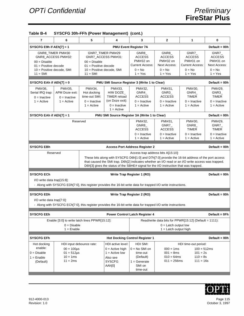
FireStar PlusOPTi Confidential Preliminary
SYSCFG E9h if AEh[7] = 1 PMU Event Register 7A Default = 00h
GNR8_TIMER PMI#30GNR8_ACCESS PMI#32:
00 = Disable01 = Positive decode10 = Positive decode, SMI11 = SMI
GNR7_TIMER PMI#29GNR7_ACCESS PMI#31:
00 = Disable01 = Positive decode10 = Positive decode, SMI11 = SMI
GNR8_ACCESS
PMI#32 on Current Access:
0 = No1 = Yes
GNR8_ACCESS
PMI#32 on Next Access:
0 = No1 = Yes
GNR7_ACCESS
PMI#31 on Current Access:
0 = No1 = Yes
GNR7_ACCESS
PMI#31 on Next Access:
0 = No1 = Yes
SYSCFG EAh if AEh[7] = 0 PMU SMI Source Register 3 (Write 1 to Clear) Default = 00h
PMI#36, Serial IRQ trap:
0 = Inactive1 = Active
PMI#35, APM Doze exit:
0 = Inactive1 = Active
PMI#34, Hot docking
time-out SMI:
0 = Inactive1 = Active
PMI#33, H/W DOZE_
TIMER reload (on Doze exit):
0 = Inactive1 = Active
PMI#32, GNR4_
ACCESS
0 = Inactive1 = Active
PMI#31, GNR3_
ACCESS
0 = Inactive1 = Active
PMI#30, GNR4_ TIMER
0 = Inactive1 = Active
PMI#29, GNR3_TIMER
0 = Inactive1 = Active
SYSCFG EAh if AEh[7] = 1 PMU SMI Source Register 3A (Write 1 to Clear) Default = 00h
Reserved PMI#32, GNR8_
ACCESS
0 = Inactive1 = Active
PMI#31, GNR7_
ACCESS
0 = Inactive1 = Active
PMI#30, GNR8_ TIMER
0 = Inactive1 = Active
PMI#29, GNR7_TIMER
0 = Inactive1 = Active
SYSCFG EBh Access Port Address Register 2 Default = 00h
Reserved Access trap address bits A[15:10]:
These bits along with SYSCFG D6h[1:0] and D7h[7:0] provide the 16-bit address of the port accessthat caused the SMI trap. D6h[2] indicates whether an I/O read or an I/O write access was trapped. D6h[3] gives the status of the SBHE# signal for the I/O instruction that was trapped.
SYSCFG ECh Write Trap Register 1 (RO) Default = 00h
I/O write data trap[15:8]:
- Along with SYSCFG EDh[7:0], this register provides the 16-bit write data for trapped I/O write instructions.
SYSCFG EDh Write Trap Register 2 (RO) Default = 00h
I/O write data trap[7:0]:
- Along with SYSCFG ECh[7:0], this register provides the 16-bit write data for trapped I/O write instructions
SYSCFG EEh Power Control Latch Register 4 Default = 0Fh
Enable [3:0] to write latch lines PPWR[15:12]:
0 = Disable1 = Enable
Read/write data bits for PPWR[15:12] (Default = 1111):
0 = Latch output low1 = Latch output high
SYSCFG EFh Hot Docking Control Register 1 Default = 00h
Hot docking enable:
0 = Disable
1 = Enable (Default)
HDI input debounce rate:
00 = 100µs01 = 512µs10 = 1ms11 = 2ms
HDI active level:
0 = Active high1 = Active low
Also see SYSCFG AAh[0]
HDI SMI:
0 = No SMI on time-out (Default)
1 = Generate SMI on time-out
HDI time-out period:
000 = 1ms 100 = 512ms001 = 8ms 101 = 2s010 = 64ms 110 = 8s011 = 256ms 111 = 16s
Table B-4 SYSCFG 30h-FFh (Power Management) (cont.)
7 6 5 4 3 2 1 0
912-4000-013 Page 115Revision: 1.0 October 3, 1997
OPTi®
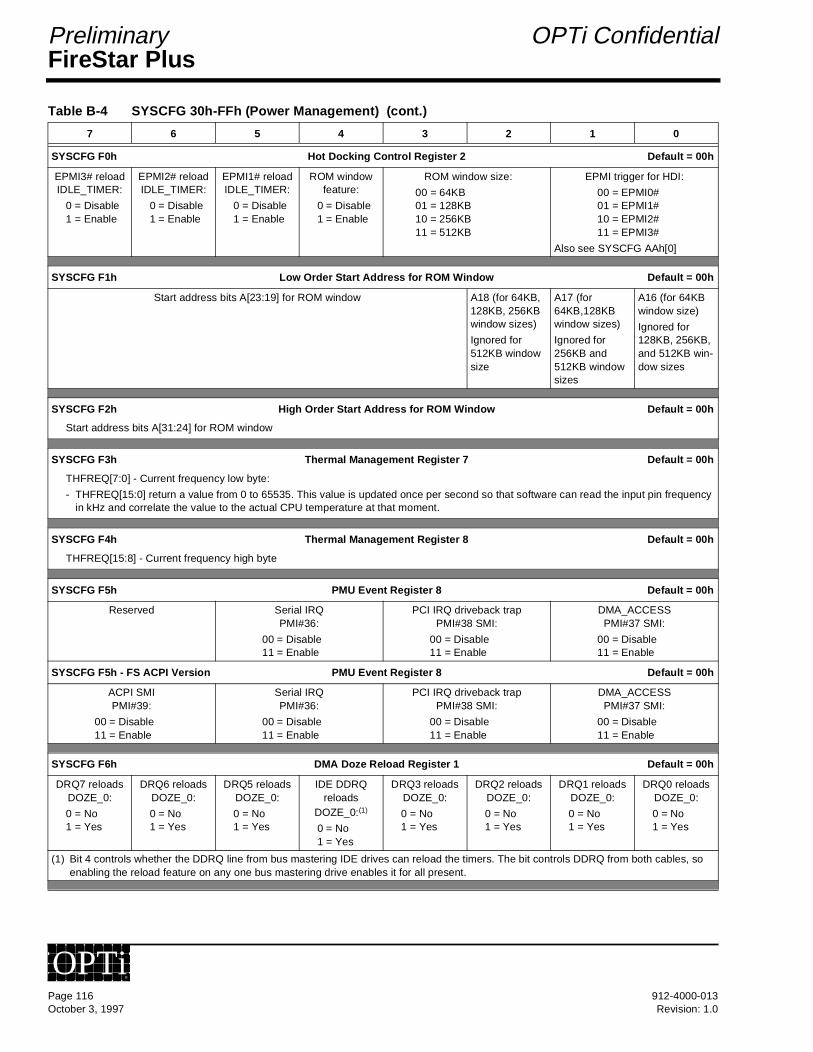
FireStar PlusPreliminary OPTi Confidential
SYSCFG F0h Hot Docking Control Register 2 Default = 00h
EPMI3# reload IDLE_TIMER:
0 = Disable1 = Enable
EPMI2# reload IDLE_TIMER:
0 = Disable1 = Enable
EPMI1# reload IDLE_TIMER:
0 = Disable1 = Enable
ROM window feature:
0 = Disable1 = Enable
ROM window size:
00 = 64KB01 = 128KB10 = 256KB11 = 512KB
EPMI trigger for HDI:
00 = EPMI0#01 = EPMI1#10 = EPMI2#11 = EPMI3#
Also see SYSCFG AAh[0]
SYSCFG F1h Low Order Start Address for ROM Window Default = 00h
Start address bits A[23:19] for ROM window A18 (for 64KB, 128KB, 256KB window sizes)
Ignored for 512KB window size
A17 (for 64KB,128KB window sizes)
Ignored for 256KB and 512KB window sizes
A16 (for 64KB window size)
Ignored for 128KB, 256KB, and 512KB win-dow sizes
SYSCFG F2h High Order Start Address for ROM Window Default = 00h
Start address bits A[31:24] for ROM window
SYSCFG F3h Thermal Management Register 7 Default = 00h
THFREQ[7:0] - Current frequency low byte:
- THFREQ[15:0] return a value from 0 to 65535. This value is updated once per second so that software can read the input pin frequency in kHz and correlate the value to the actual CPU temperature at that moment.
SYSCFG F4h Thermal Management Register 8 Default = 00h
THFREQ[15:8] - Current frequency high byte
SYSCFG F5h PMU Event Register 8 Default = 00h
Reserved Serial IRQ PMI#36:
00 = Disable11 = Enable
PCI IRQ driveback trap PMI#38 SMI:
00 = Disable11 = Enable
DMA_ACCESS PMI#37 SMI:
00 = Disable11 = Enable
SYSCFG F5h - FS ACPI Version PMU Event Register 8 Default = 00h
ACPI SMIPMI#39:
00 = Disable11 = Enable
Serial IRQ PMI#36:
00 = Disable11 = Enable
PCI IRQ driveback trap PMI#38 SMI:
00 = Disable11 = Enable
DMA_ACCESS PMI#37 SMI:
00 = Disable11 = Enable
SYSCFG F6h DMA Doze Reload Register 1 Default = 00h
DRQ7 reloads DOZE_0:
0 = No1 = Yes
DRQ6 reloads DOZE_0:
0 = No1 = Yes
DRQ5 reloads DOZE_0:
0 = No1 = Yes
IDE DDRQ reloads
DOZE_0:(1)
0 = No1 = Yes
DRQ3 reloads DOZE_0:
0 = No1 = Yes
DRQ2 reloads DOZE_0:
0 = No1 = Yes
DRQ1 reloads DOZE_0:
0 = No1 = Yes
DRQ0 reloads DOZE_0:
0 = No1 = Yes
(1) Bit 4 controls whether the DDRQ line from bus mastering IDE drives can reload the timers. The bit controls DDRQ from both cables, so enabling the reload feature on any one bus mastering drive enables it for all present.
Table B-4 SYSCFG 30h-FFh (Power Management) (cont.)
7 6 5 4 3 2 1 0
Page 116 912-4000-013October 3, 1997 Revision: 1.0
OPTi®
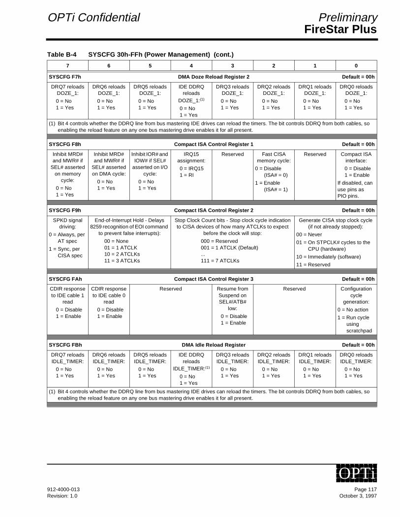
FireStar PlusOPTi Confidential Preliminary
SYSCFG F7h DMA Doze Reload Register 2 Default = 00h
DRQ7 reloads DOZE_1:
0 = No1 = Yes
DRQ6 reloads DOZE_1:
0 = No1 = Yes
DRQ5 reloads DOZE_1:
0 = No1 = Yes
IDE DDRQ reloads
DOZE_1:(1)
0 = No1 = Yes
DRQ3 reloads DOZE_1:
0 = No1 = Yes
DRQ2 reloads DOZE_1:
0 = No1 = Yes
DRQ1 reloads DOZE_1:
0 = No1 = Yes
DRQ0 reloads DOZE_1:
0 = No1 = Yes
(1) Bit 4 controls whether the DDRQ line from bus mastering IDE drives can reload the timers. The bit controls DDRQ from both cables, so enabling the reload feature on any one bus mastering drive enables it for all present.
SYSCFG F8h Compact ISA Control Register 1 Default = 00h
Inhibit MRD# and MWR# if
SEL# asserted on memory
cycle:
0 = No1 = Yes
Inhibit MRD# and MWR# if
SEL# asserted on DMA cycle:
0 = No1 = Yes
Inhibit IOR# and IOW# if SEL#
asserted on I/O cycle:
0 = No1 = Yes
IRQ15 assignment:
0 = IRQ151 = RI
Reserved Fast CISA memory cycle:
0 = Disable (ISA# = 0)
1 = Enable (ISA# = 1)
Reserved Compact ISA interface:
0 = Disable1 = Enable
If disabled, can use pins as PIO pins.
SYSCFG F9h Compact ISA Control Register 2 Default = 00h
SPKD signal driving:
0 = Always, per AT spec
1 = Sync, per CISA spec
End-of-Interrupt Hold - Delays 8259 recognition of EOI command
to prevent false interrupts):
00 = None01 = 1 ATCLK10 = 2 ATCLKs11 = 3 ATCLKs
Stop Clock Count bits - Stop clock cycle indication to CISA devices of how many ATCLKs to expect
before the clock will stop:
000 = Reserved001 = 1 ATCLK (Default)...111 = 7 ATCLKs
Generate CISA stop clock cycle (if not already stopped):
00 = Never
01 = On STPCLK# cycles to the CPU (hardware)
10 = Immediately (software)
11 = Reserved
SYSCFG FAh Compact ISA Control Register 3 Default = 00h
CDIR response to IDE cable 1
read
0 = Disable1 = Enable
CDIR response to IDE cable 0
read
0 = Disable1 = Enable
Reserved Resume from Suspend on SEL#/ATB#
low:
0 = Disable1 = Enable
Reserved Configuration cycle
generation:
0 = No action
1 = Run cycle using scratchpad
SYSCFG FBh DMA Idle Reload Register Default = 00h
DRQ7 reloads IDLE_TIMER:
0 = No1 = Yes
DRQ6 reloads IDLE_TIMER:
0 = No1 = Yes
DRQ5 reloads IDLE_TIMER:
0 = No1 = Yes
IDE DDRQ reloads
IDLE_TIMER:(1)
0 = No1 = Yes
DRQ3 reloads IDLE_TIMER:
0 = No1 = Yes
DRQ2 reloads IDLE_TIMER:
0 = No1 = Yes
DRQ1 reloads IDLE_TIMER:
0 = No1 = Yes
DRQ0 reloads IDLE_TIMER:
0 = No1 = Yes
(1) Bit 4 controls whether the DDRQ line from bus mastering IDE drives can reload the timers. The bit controls DDRQ from both cables, so enabling the reload feature on any one bus mastering drive enables it for all present.
Table B-4 SYSCFG 30h-FFh (Power Management) (cont.)
7 6 5 4 3 2 1 0
912-4000-013 Page 117Revision: 1.0 October 3, 1997
OPTi®
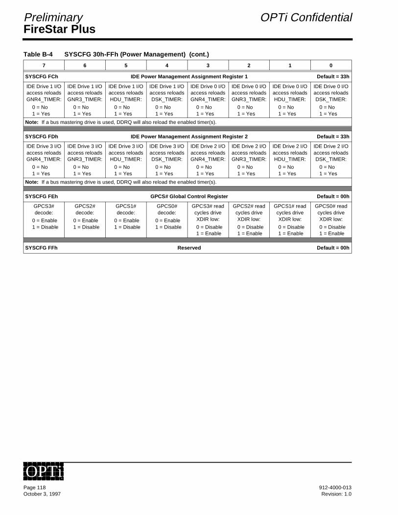
FireStar PlusPreliminary OPTi Confidential
SYSCFG FCh IDE Power Management Assignment Register 1 Default = 33h
IDE Drive 1 I/O access reloads GNR4_TIMER:
0 = No1 = Yes
IDE Drive 1 I/O access reloads GNR3_TIMER:
0 = No1 = Yes
IDE Drive 1 I/O access reloads HDU_TIMER:
0 = No1 = Yes
IDE Drive 1 I/O access reloads DSK_TIMER:
0 = No1 = Yes
IDE Drive 0 I/O access reloads GNR4_TIMER:
0 = No1 = Yes
IDE Drive 0 I/O access reloads GNR3_TIMER:
0 = No1 = Yes
IDE Drive 0 I/O access reloads HDU_TIMER:
0 = No1 = Yes
IDE Drive 0 I/O access reloads DSK_TIMER:
0 = No1 = Yes
Note: If a bus mastering drive is used, DDRQ will also reload the enabled timer(s).
SYSCFG FDh IDE Power Management Assignment Register 2 Default = 33h
IDE Drive 3 I/O access reloads GNR4_TIMER:
0 = No1 = Yes
IDE Drive 3 I/O access reloads GNR3_TIMER:
0 = No1 = Yes
IDE Drive 3 I/O access reloads HDU_TIMER:
0 = No1 = Yes
IDE Drive 3 I/O access reloads DSK_TIMER:
0 = No1 = Yes
IDE Drive 2 I/O access reloads GNR4_TIMER:
0 = No1 = Yes
IDE Drive 2 I/O access reloads GNR3_TIMER:
0 = No1 = Yes
IDE Drive 2 I/O access reloads HDU_TIMER:
0 = No1 = Yes
IDE Drive 2 I/O access reloads DSK_TIMER:
0 = No1 = Yes
Note: If a bus mastering drive is used, DDRQ will also reload the enabled timer(s).
SYSCFG FEh GPCS# Global Control Register Default = 00h
GPCS3# decode:
0 = Enable1 = Disable
GPCS2# decode:
0 = Enable1 = Disable
GPCS1# decode:
0 = Enable1 = Disable
GPCS0# decode:
0 = Enable1 = Disable
GPCS3# read cycles drive XDIR low:
0 = Disable1 = Enable
GPCS2# read cycles drive XDIR low:
0 = Disable1 = Enable
GPCS1# read cycles drive XDIR low:
0 = Disable1 = Enable
GPCS0# read cycles drive XDIR low:
0 = Disable1 = Enable
SYSCFG FFh Reserved Default = 00h
Table B-4 SYSCFG 30h-FFh (Power Management) (cont.)
7 6 5 4 3 2 1 0
Page 118 912-4000-013October 3, 1997 Revision: 1.0
OPTi®

FireStar PlusOPTi Confidential Preliminary
B.3 PCIDV1 Register SpaceThe PCI Configuration Register Space designated asPCIDV1 is accessed through Configuration Mechanism #1 asBus #0, Device #1, and Function #0.
PCIDV1 00h-3Fh are PCI-specific related registers whilePCIDV1 40h-FFh are system control related registers. TableB-5 gives the bit formats for these registers.
Table B-5 PCIDV1 00h-FFh
7 6 5 4 3 2 1 0
PCIDV1 00h Vendor Identification Register (RO) - Byte 0 Default = 45h
PCIDV1 01h Vendor Identification Register (RO) - Byte 1 Default = 10h
PCIDV1 02h Device Identification Register (RO) - Byte 0 Default = 00h
PCIDV1 03h Device Identification Register (RO) - Byte 1 Default = C7h
PCIDV1 04h Command Register - Byte 0 Default = 07h
Address/data stepping (RO):
0 = Disable(always)
PERR# output pin:
0 = Disable1 = Enable
Reserved Memory write and invalidate cycle genera-
tion (RO):
Must = 0(always)
No memory write and invali-date cycles will be generated by the 82C700.
Special cycles (R/W):
The 82C700 does not respond to the PCI special cycle.
Bus master operations
(R/W):
This allows the 82C700 to per-form bus master operations at any time.
(Default = 1)
Memory access (RO):
Must = 1(always)
The 82C700 allows a PCI bus master access to mem-ory at anytime.
(Default = 1)
I/O access (RO):
Must = 1(always)
The 82C700 allows a PCI bus master I/O access at any time.
(Default = 1)
PCIDV1 05h Command Register - Byte 1 Default = 00h
Reserved Fast back-to-back to differ-
ent slaves (RO):
0 = Disable1 = Enable
SERR# output pin:
0 = Disable1 = Enable
PCIDV1 06h Status Register - Byte 0 Default = 80h
Fast back-to-back capability
(RO):
0 = Not Capable1 = Capable(Default = 1)
Also see PCIDV1 46h[2].
Reserved
PCIDV1 07h Status Register - Byte 1 Default = 02h
Parity error detected:
0 = No1 = Yes
SERR# status (RO):
Must = 0(always)
Master abort status (RO):
Must = 0(always)
Received target abort status (RO):
0 = No target abort
1 = Target abort occurred
Signaled target abort status
(RO):
Must = 0 (always)
DEVSEL# timing status (RO):
Must = 01 (always)
Indicates medium timing selec-tion; the 82C700 asserts the DEVSEL# based on medium timing.
(Default = 01)
Data parity error detected:
0 = No1 = Yes
912-4000-013 Page 119Revision: 1.0 October 3, 1997
OPTi®

FireStar PlusPreliminary OPTi Confidential
PCIDV1 08h Revision Identification Register (RO) Default = 10h
- The chip revision number in the PCI configuration space consists of two parts: a major revision number and a minor revision number. The 8-bit register is interpreted as x.yh, where for example revision 2.1 of the chip would be read as two BCD digits, 0010 0001b. Software programmers must take care in using the minor revision number, because the number may change between register- and software-equivalent versions of the chip.
PCIDV1 09h Class Code Register (RO) - Byte 0 Default = 00h
PCIDV1 0Ah Class Code Register (RO) - Byte 1 Default = 00h
PCIDV1 0Bh Class Code Register (RO) - Byte 2 Default = 06h
PCIDV1 0Ch Reserved Default = 00h
PCIDV1 0Dh Master Latency Timer Register (RO) Default = 00h
PCIDV1 0Eh Header Type Register (RO) Default = 00h
PCIDV1 0Fh Built-In Self-Test (BIST) Register (RO) Default = 00h
PCIDV1 10h-2Bh Reserved Default = 00h
PCIDV1 2Ch-2Dh Subsystem Vendor ID Default = 00h
(Write one time only)
PCIDV1 2Eh-2Fh Subsystem ID Default = 00h
(Write one time only)
PCIDV1 30h-40h Reserved Default = 00h
PCIDV1 41h Keyboard Controller Select Register Default = 00h
RDKBDPRT (RO):
Keyboard con-troller has received Com-mand D0h and has not received the fol-lowing 060h read.
WRKBDPRT (RO):
Keyboard con-troller has received Com-mand D1h and has not received the fol-lowing 060h write.
IMMINIT: Generate INIT immediately on FEh Command.
0 = Generate INIT imme-diately on FEh Com-mand
1 = Wait for halt before INIT for key-board reset
KBDEMU: Keyboard emulation
0 = Enable1 = Disable
KBDCS# includes Port
062h and 066h
0 = Disable 1 = Enable
Reserved
PCIDV1 42h Reserved Default = 00h
Table B-5 PCIDV1 00h-FFh (cont.)
7 6 5 4 3 2 1 0
Page 120 912-4000-013October 3, 1997 Revision: 1.0
OPTi®

FireStar PlusOPTi Confidential Preliminary
PCIDV1 43h Feature Control Register Default = 00h
Buffered DMA (data transfer to/from DRAM through PCI master):
00 = Original DMA with old protocol
01 = Reserved
10 = Original DMA with PCI master capability
11 = Buffered DMA enable
Enable DMA or ISA master to preempt PCI
master:
0 = Disable1 = Enable
Fixed/rotating priority
between PCI masters:
0 = Rotating 1 = Fixed
Back-to-back ISA I/O cycle delay:
00 = Delay by 3 ATCLKs
01 = Delay by 12 ATCLKs
10 = No delay
11 = Delay by 12 ATCLKs(1)
PCI master access to
ISA:
0 = Enable1 = Disable
ISA bus control signals for memory accesses
greater than 16M:
0 = Enable1 = Disable
(1) When bits [3:2] take on the combination of 11, all back-to-back cycles are delayed by 12 AT clocks. This is different from the combinations of 00 and 01 because in the latter case, the delay will be inserted only when an I/O access is followed by a second I/O access with no other type of access occurring in between (e.g., a memory access).
PCIDV1 44h-45h Reserved Default = 00h
PCIDV1 46h PCI Control Register B - Byte 0 Default = 06h
DMA/ISA access to PCI slave:
0 = Never
1 = When inter-nal LMEM# is not asserted
Master retry always unmasked after 16 PCICLKs.
XDIR control:
0 = XDIR is controlled for accesses to/from ROM, Kybd controller, RTC
1 = XDIR is controlled only during access to/from ROM
Conversion of PERR# to SERR#:
0 = Disable1 = Enable
Address parity checking:
0 = Disable1 = Enable
Generation of SERR# for
target abort:
0 = Disable1 = Enable
Fast back-to-back capability:
0 = Disable1 = Enable
Note: The change on this bit will reflect in PCIDV1 06h[7].
Subtractive decoding
sample point:
0 = Typical sample point
1 = Slow sam-ple point
Reserved
PCIDV1 47h PCI Control Register B - Byte 1 Default = 00h
Write protect ISA bus ROM:
0 = Disable ROMCS# for writes
1 = Enable ROMCS# for writes
Hidden refresh:
0 = Normal refresh
1 = Hidden refresh
Hidden refresh is not sup-ported - never set this bit to 1.
ATCLK frequency:
00 = PCICLK ÷401 = PCICLK ÷310 = PCICLK ÷211 = PCICLK
CPU master to PCI slave write:
(turnaround between
address and data phases)
0 = 1 PCICLK 1 = 0 PCICLK
PCI master to PCI master preemption timer: (preempt after unserviced request pending
for X PCICLKs)
000 = No Preemption 100 = 36 PCICLKs001 = 260 PCICLKs 101 = 20 PCICLKs010 = 132 PCICLKs 110 = 12 PCICLKs011 = 68 PCICLKs 111 = 5 PCICLKs
PCIDV1 48h Strap Option Readback Register - Byte 0 Default = 00h
Reserved IGERR# strap option selects:
0 = 5.0V ISA1 = 3.3V ISA
NMI strap option selects:
0 = 5.0V DRAM1 = 3.3V DRAM
INTR strap option selects:
0 = 5.0V PCI1 = 3.3V PCI
ROMCS#:KBDCS# strap option selects:
00 = CMD#, ATCLK, BALE
01 = PCICLK3, ATCLK, BALE
10 = PCICLK3, PCICLK4, BALE
11 = PCICLK3, PCICLK4, PCICLK5
RTCWR# strap option selects:
0 = GNT2#1 = PCICLK2
RTCRD# strap option selects:
0 = GNT1#1 = PCICLK1
Table B-5 PCIDV1 00h-FFh (cont.)
7 6 5 4 3 2 1 0
912-4000-013 Page 121Revision: 1.0 October 3, 1997
OPTi®
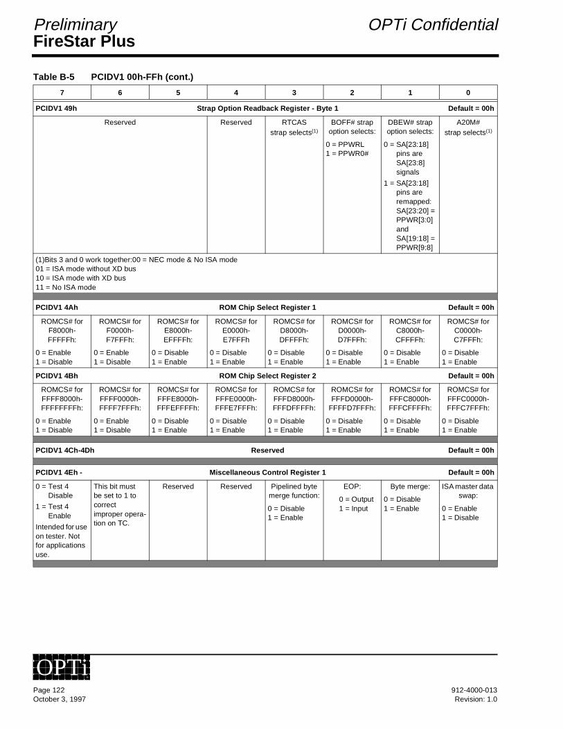
FireStar PlusPreliminary OPTi Confidential
PCIDV1 49h Strap Option Readback Register - Byte 1 Default = 00h
Reserved Reserved RTCAS strap selects(1)
BOFF# strap option selects:
0 = PPWRL1 = PPWR0#
DBEW# strap option selects:
0 = SA[23:18] pins are SA[23:8] signals
1 = SA[23:18] pins are remapped: SA[23:20] = PPWR[3:0] and SA[19:18] = PPWR[9:8]
A20M# strap selects(1)
(1)Bits 3 and 0 work together:00 = NEC mode & No ISA mode 01 = ISA mode without XD bus10 = ISA mode with XD bus11 = No ISA mode
PCIDV1 4Ah ROM Chip Select Register 1 Default = 00h
ROMCS# for F8000h-FFFFFh:
0 = Enable1 = Disable
ROMCS# for F0000h-F7FFFh:
0 = Enable1 = Disable
ROMCS# for E8000h-EFFFFh:
0 = Disable1 = Enable
ROMCS# for E0000h-E7FFFh
0 = Disable1 = Enable
ROMCS# for D8000h-DFFFFh:
0 = Disable1 = Enable
ROMCS# for D0000h-D7FFFh:
0 = Disable1 = Enable
ROMCS# for C8000h-CFFFFh:
0 = Disable1 = Enable
ROMCS# for C0000h-C7FFFh:
0 = Disable1 = Enable
PCIDV1 4Bh ROM Chip Select Register 2 Default = 00h
ROMCS# for FFFF8000h-FFFFFFFFh:
0 = Enable1 = Disable
ROMCS# for FFFF0000h-FFFF7FFFh:
0 = Enable1 = Disable
ROMCS# for FFFE8000h-FFFEFFFFh:
0 = Disable1 = Enable
ROMCS# for FFFE0000h-FFFE7FFFh:
0 = Disable1 = Enable
ROMCS# for FFFD8000h-FFFDFFFFh:
0 = Disable1 = Enable
ROMCS# for FFFD0000h-
FFFFD7FFFh:
0 = Disable1 = Enable
ROMCS# for FFFC8000h-FFFCFFFFh:
0 = Disable1 = Enable
ROMCS# for FFFC0000h-FFFC7FFFh:
0 = Disable1 = Enable
PCIDV1 4Ch-4Dh Reserved Default = 00h
PCIDV1 4Eh - Miscellaneous Control Register 1 Default = 00h
0 = Test 4 Disable
1 = Test 4 Enable
Intended for use on tester. Not for applications use.
This bit must be set to 1 to correct improper opera-tion on TC.
Reserved Reserved Pipelined byte merge function:
0 = Disable1 = Enable
EOP:
0 = Output1 = Input
Byte merge:
0 = Disable1 = Enable
ISA master data swap:
0 = Enable1 = Disable
Table B-5 PCIDV1 00h-FFh (cont.)
7 6 5 4 3 2 1 0
Page 122 912-4000-013October 3, 1997 Revision: 1.0
OPTi®

FireStar PlusOPTi Confidential Preliminary
PCIDV1 4Fh - Miscellaneous Control Register 2 Default = 20h
Allow IRQA, B,...H PCI
IRQs (when programed as level IRQs) tobe shareable with PIO PCI
IRQ pins:
0 = Disable1 = Enable
IDE interface:
0 = Disable1 = Enable
Primary IDE interface (1F0h):
0 = Disable
1 = Enable (Default)
AT clock wait state control:
0 = Extra WS for ISA cycles
1 = No extra WS
Context Save mode:
0 = Disable1 = Enable
Timer positive decode in
PC98 mode (I/O 77h, 75h, 73h,
71h):
0 = Disable, decode 1 CLK after subtractive decode
1 = Enable, medium decode and remap to 43h, 42h, 41h, and 40h
ROMCS#, KBDCS#, and DBEW# pin selections:(1)
BIOS access after soft reset:
0 = ROM1 = DRAM
(1)0 =ROMCS# pin can be ROMCS# or PIO23 if PCIDV1 52h[2] = 0ROMCS# pin can be ROMCS# and KBDCS# if PCIDV1 52h[2] = 1KBDCS# pin can be KBDCS# or PIO24DBEW# pin is DBEW#
1 =ROMCS# pin is ROMCS# and KBDCS# if PCIDV1 52h[2] = 0 or 1KBDCS# pin is DRD#DBEW# is DWR#Note: Also see PCIDV1 52h[2].
PCIDV1 50h-51h Reserved Default = 00h
PCIDV1 52h - Miscellaneous Controller Register 3 Default = 00h
TC/IDEDIR enable:
0 = Only TC will be generated on this pin
1 =Both TC and IDEDIR will be gener-ayed on thsi pin.
This bit should be set to 1, if UltraDMA func-tionality is required.
STOP# genera-tion for BDMA
transfers past a cache line.
0 =no STOP# generation1 = STOP# gen-eration enabled
Reserved Abort DDMA remap cycle if
claimed by Firestar:
0 = Disable1 = Enable
Rsvd pin (A7)function:
0 = Rsvd 1 = SDCKE
ROMCS# pin selection:
0 = Controlled by PCIDV1 4Fh[1]
1 = ROMCS# pin is always ROMCS# and KBDCS#
Note: Also see PCIDV1 4Fh[1]
Priority scheme:
0 = Disable1 = Enable
A setting of 1 will employ a priority scheme that guarantees higher priority for PCI masters during arbitra-tion over DMA and ISA mas-ters for the first 7µs interval after every refresh cycle.
Concurrent refresh and IDE cycle:
0 = Disable1 = Enable
ISA devices that rely on accu-rate refresh addresses for proper opera-tion should dis-able this bit.
Table B-5 PCIDV1 00h-FFh (cont.)
7 6 5 4 3 2 1 0
912-4000-013 Page 123Revision: 1.0 October 3, 1997
OPTi®
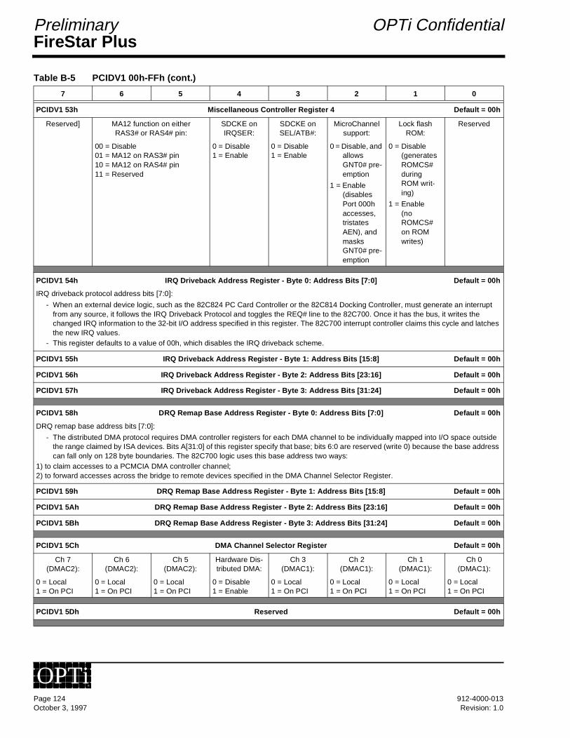
FireStar PlusPreliminary OPTi Confidential
PCIDV1 53h Miscellaneous Controller Register 4 Default = 00h
Reserved] MA12 function on either RAS3# or RAS4# pin:
00 = Disable01 = MA12 on RAS3# pin10 = MA12 on RAS4# pin11 = Reserved
SDCKE on IRQSER:
0 = Disable1 = Enable
SDCKE on SEL/ATB#:
0 = Disable1 = Enable
MicroChannel support:
0 = Disable, and allows GNT0# pre-emption
1 = Enable (disables Port 000h accesses, tristates AEN), and masks GNT0# pre-emption
Lock flash ROM:
0 = Disable (generates ROMCS# during ROM writ-ing)
1 = Enable (no ROMCS# on ROM writes)
Reserved
PCIDV1 54h IRQ Driveback Address Register - Byte 0: Address Bits [7:0] Default = 00h
IRQ driveback protocol address bits [7:0]:
- When an external device logic, such as the 82C824 PC Card Controller or the 82C814 Docking Controller, must generate an interrupt from any source, it follows the IRQ Driveback Protocol and toggles the REQ# line to the 82C700. Once it has the bus, it writes the changed IRQ information to the 32-bit I/O address specified in this register. The 82C700 interrupt controller claims this cycle and latches the new IRQ values.
- This register defaults to a value of 00h, which disables the IRQ driveback scheme.
PCIDV1 55h IRQ Driveback Address Register - Byte 1: Address Bits [15:8] Default = 00h
PCIDV1 56h IRQ Driveback Address Register - Byte 2: Address Bits [23:16] Default = 00h
PCIDV1 57h IRQ Driveback Address Register - Byte 3: Address Bits [31:24] Default = 00h
PCIDV1 58h DRQ Remap Base Address Register - Byte 0: Address Bits [7:0] Default = 00h
DRQ remap base address bits [7:0]:
- The distributed DMA protocol requires DMA controller registers for each DMA channel to be individually mapped into I/O space outside the range claimed by ISA devices. Bits A[31:0] of this register specify that base; bits 6:0 are reserved (write 0) because the base address can fall only on 128 byte boundaries. The 82C700 logic uses this base address two ways:
1) to claim accesses to a PCMCIA DMA controller channel; 2) to forward accesses across the bridge to remote devices specified in the DMA Channel Selector Register.
PCIDV1 59h DRQ Remap Base Address Register - Byte 1: Address Bits [15:8] Default = 00h
PCIDV1 5Ah DRQ Remap Base Address Register - Byte 2: Address Bits [23:16] Default = 00h
PCIDV1 5Bh DRQ Remap Base Address Register - Byte 3: Address Bits [31:24] Default = 00h
PCIDV1 5Ch DMA Channel Selector Register Default = 00h
Ch 7 (DMAC2):
0 = Local1 = On PCI
Ch 6 (DMAC2):
0 = Local1 = On PCI
Ch 5 (DMAC2):
0 = Local1 = On PCI
Hardware Dis-tributed DMA:
0 = Disable1 = Enable
Ch 3 (DMAC1):
0 = Local1 = On PCI
Ch 2 (DMAC1):
0 = Local1 = On PCI
Ch 1 (DMAC1):
0 = Local1 = On PCI
Ch 0 (DMAC1):
0 = Local1 = On PCI
PCIDV1 5Dh Reserved Default = 00h
Table B-5 PCIDV1 00h-FFh (cont.)
7 6 5 4 3 2 1 0
Page 124 912-4000-013October 3, 1997 Revision: 1.0
OPTi®
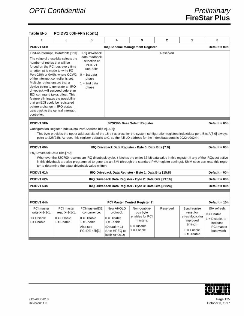
FireStar PlusOPTi Confidential Preliminary
PCIDV1 5Eh IRQ Scheme Management Register Default = 00h
End-of-Interrupt Holdoff bits [1:0]:
The value of these bits selects the number of retries that will be forced on the PCI bus every time an attempt is made to write I/O Port 020h or 0A0h, where OCW2 of the interrupt controller is set. Multiple retries ensure that a device trying to generate an IRQ driveback will succeed before an EOI command takes effect. This feature eliminates the possibility that an EOI could be registered before a change in IRQ status gets back to the central interrupt controller.
IRQ driveback data readback
selection at PCIDV1 60h-63h:
0 = 1st data phase
1 = 2nd data phase
Reserved
PCIDV1 5Fh SYSCFG Base Select Register Default = 00h
Configuration Register Index/Data Port Address bits A[15:8]:
- This byte provides the upper address bits of the 16-bit address for the system configuration registers index/data port. Bits A[7:0] always point to 22h/24h. At reset, this register defaults to 0, so the full I/O address for the index/data ports is 0022h/0024h.
PCIDV1 60h IRQ Driveback Data Register - Byte 0: Data Bits [7:0] Default = 00h
IRQ Driveback Data Bits [7:0]:
- Whenever the 82C700 receives an IRQ driveback cycle, it latches the entire 32-bit data value in this register. If any of the IRQs set active in this driveback are also programmed to generate an SMI (through the standard PMU register settings), SMM code can read this regis-ter to determine the exact driveback value written.
PCIDV1 61h IRQ Driveback Data Register - Byte 1: Data Bits [15:8] Default = 00h
PCIDV1 62h IRQ Driveback Data Register - Byte 2: Data Bits [23:16] Default = 00h
PCIDV1 63h IRQ Driveback Data Register - Byte 3: Data Bits [31:24] Default = 00h
PCIDV1 64h PCI Master Control Register 2] Default = 10h
PCI master write X-1-1-1:
0 = Disable1 = Enable
PCI master read X-1-1-1:
0 = Disable1 = Enable
PCI master/IDE concurrence:
0 = Disable1 = Enable
Also see PCIIDE 42h[3]
New AHOLD protocol:
0 = Disable1 = Enable
(Default = 1)(Use HREQ to latch AHOLD)
Non-contigu-ous byte
enables for PCI masters:
0 = Disable1 = Enable
Reserved Synchronize reset for
refresh logic (for improved timing):
0 = Enable1 = Disable
ISA refresh:
0 = Enable
1 = Disable, to increase PCI master bandwidth
Table B-5 PCIDV1 00h-FFh (cont.)
7 6 5 4 3 2 1 0
912-4000-013 Page 125Revision: 1.0 October 3, 1997
OPTi®
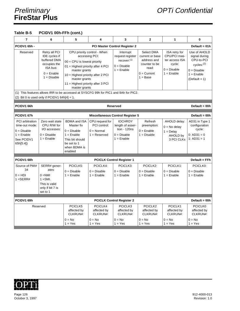
FireStar PlusPreliminary OPTi Confidential
PCIDV1 65h - PCI Master Control Register 2 Default = 01h
Reserved Retry all PCI IDE cycles if
buffered DMA occupies the
ISA bus:
0 = Enable1 = Disable
CPU priority control - When accessing PCI:
00 = CPU is lowest priority
01 = Highest priority after 4 PCI master grants
10 = Highest priority after 2 PCI master grants
11 = Highest priority after 3 PCI master grants
Interrupt request register
recover:(1)
0 = Disable1 = Enable
Select DMA current or base
address and counter to be
read:
0 = Current1 = Base
ISA retry for CPU/PCI mas-ter access ISA
cycle:
0 = Disable1 = Enable
Use of AHOLD signal during CPU-to-PCI
cycles:(2)
0 = Disable1 = Enable
(Default = 1)
(1) This features allows IRR to be accessed at SYSCFG 99h for PIC1 and 9Ah for PIC2.
(2) Bit 0 is used only if PCIDV1 64h[4] = 1.
PCIDV1 66h Reserved Default = 00h
PCIDV1 67h Miscellaneous Control Register 5 Default = 00h
PCI arbitration time-out mode:
0 = Disable1 = Enable
See PCIDV1 65h[5:4])
Zero wait state CPU R/W for I/O accesses:
0 = Disable1 = Enable
BDMA and ISA Master fix
0 = Disable1 = Enable
This bit should be set to 1 when BDMA is enabled
CPU request for PCI control:
0 = Normal1 = Reserved
IOCHRDY length of asser-
tion - 120ns
0 = Disable1 = Enable
Refresh preemption:
0 = Enable1 = Disable
AHOLD delay:
0 = No delay
1 = Delay AHOLD by 3 PCI CLKs
AD31 in Type 1 configuration
cycle:
0: AD31 = 01: AD31 = 1
PCIDV1 68h PCICLK Control Register 1 Default = FFh
Source of PMI# 34
0 = HDI1 =SERR#
SERR# gener-ates:
0 =NMI1 =SMI.
This is valid only if bit 7 is set to 1
PCICLK5:
0 = Disable1 = Enable
PCICLK4:
0 = Disable1 = Enable
PCICLK3:
0 = Disable1 = Enable
PCICLK2:
0 = Disable1 = Enable
PCICLK1:
0 = Disable1 = Enable
PCICLK0:
0 = Disable1 = Enable
PCIDV1 69h PCICLK Control Register 2 Default = 00h
Reserved PCICLK5 affected by CLKRUN#:
0 = No1 = Yes
PCICLK4 affected by CLKRUN#:
0 = No1 = Yes
PCICLK3 affected by CLKRUN#:
0 = No1 = Yes
PCICLK2 affected by CLKRUN#:
0 = No1 = Yes
PCICLK1 affected by CLKRUN#:
0 = No1 = Yes
PCICLK0 affected by CLKRUN#:
0 = No1 = Yes
Table B-5 PCIDV1 00h-FFh (cont.)
7 6 5 4 3 2 1 0
Page 126 912-4000-013October 3, 1997 Revision: 1.0
OPTi®
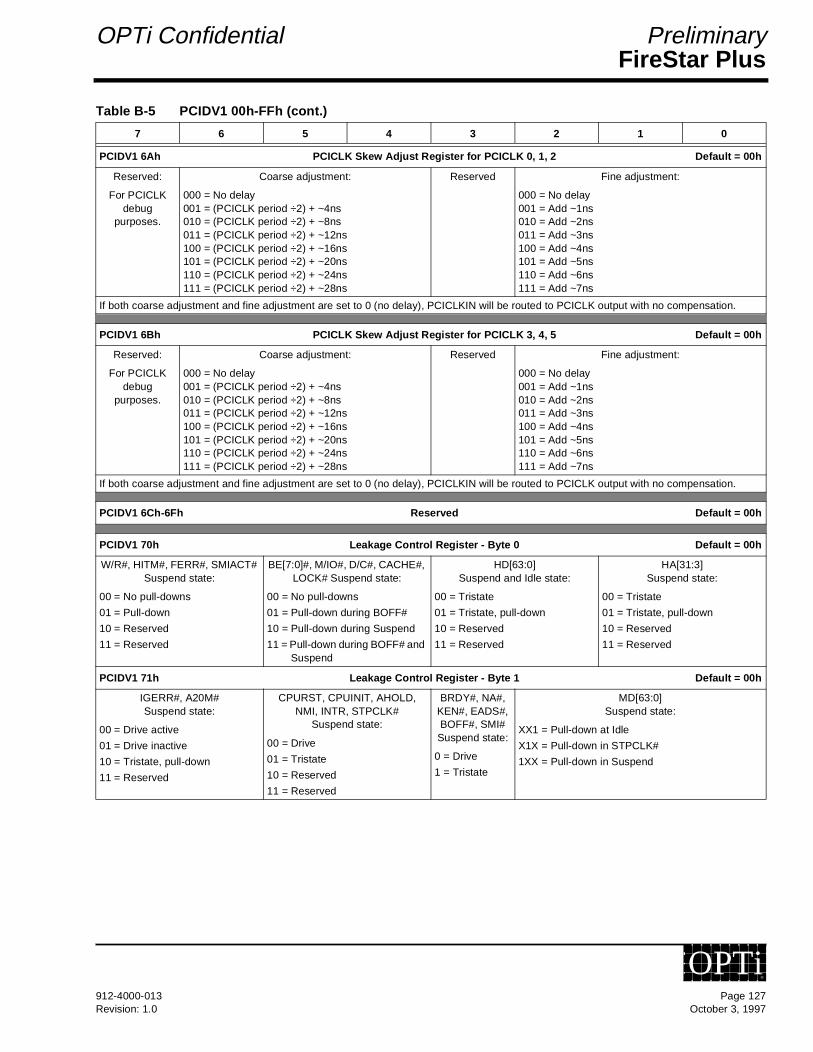
FireStar PlusOPTi Confidential Preliminary
PCIDV1 6Ah PCICLK Skew Adjust Register for PCICLK 0, 1, 2 Default = 00h
Reserved:
For PCICLK debug
purposes.
Coarse adjustment:
000 = No delay001 = (PCICLK period ÷2) + ~4ns010 = (PCICLK period ÷2) + ~8ns011 = (PCICLK period ÷2) + ~12ns100 = (PCICLK period ÷2) + ~16ns101 = (PCICLK period ÷2) + ~20ns110 = (PCICLK period ÷2) + ~24ns111 = (PCICLK period ÷2) + ~28ns
Reserved Fine adjustment:
000 = No delay001 = Add ~1ns010 = Add ~2ns011 = Add ~3ns100 = Add ~4ns101 = Add ~5ns110 = Add ~6ns111 = Add ~7ns
If both coarse adjustment and fine adjustment are set to 0 (no delay), PCICLKIN will be routed to PCICLK output with no compensation.
PCIDV1 6Bh PCICLK Skew Adjust Register for PCICLK 3, 4, 5 Default = 00h
Reserved:
For PCICLK debug
purposes.
Coarse adjustment:
000 = No delay001 = (PCICLK period ÷2) + ~4ns010 = (PCICLK period ÷2) + ~8ns011 = (PCICLK period ÷2) + ~12ns100 = (PCICLK period ÷2) + ~16ns101 = (PCICLK period ÷2) + ~20ns110 = (PCICLK period ÷2) + ~24ns111 = (PCICLK period ÷2) + ~28ns
Reserved Fine adjustment:
000 = No delay001 = Add ~1ns010 = Add ~2ns011 = Add ~3ns100 = Add ~4ns101 = Add ~5ns110 = Add ~6ns111 = Add ~7ns
If both coarse adjustment and fine adjustment are set to 0 (no delay), PCICLKIN will be routed to PCICLK output with no compensation.
PCIDV1 6Ch-6Fh Reserved Default = 00h
PCIDV1 70h Leakage Control Register - Byte 0 Default = 00h
W/R#, HITM#, FERR#, SMIACT# Suspend state:
00 = No pull-downs
01 = Pull-down
10 = Reserved
11 = Reserved
BE[7:0]#, M/IO#, D/C#, CACHE#, LOCK# Suspend state:
00 = No pull-downs
01 = Pull-down during BOFF#
10 = Pull-down during Suspend
11 = Pull-down during BOFF# and Suspend
HD[63:0] Suspend and Idle state:
00 = Tristate
01 = Tristate, pull-down
10 = Reserved
11 = Reserved
HA[31:3] Suspend state:
00 = Tristate
01 = Tristate, pull-down
10 = Reserved
11 = Reserved
PCIDV1 71h Leakage Control Register - Byte 1 Default = 00h
IGERR#, A20M# Suspend state:
00 = Drive active
01 = Drive inactive
10 = Tristate, pull-down
11 = Reserved
CPURST, CPUINIT, AHOLD, NMI, INTR, STPCLK#
Suspend state:
00 = Drive
01 = Tristate
10 = Reserved
11 = Reserved
BRDY#, NA#, KEN#, EADS#, BOFF#, SMI# Suspend state:
0 = Drive
1 = Tristate
MD[63:0] Suspend state:
XX1 = Pull-down at Idle
X1X = Pull-down in STPCLK#
1XX = Pull-down in Suspend
Table B-5 PCIDV1 00h-FFh (cont.)
7 6 5 4 3 2 1 0
912-4000-013 Page 127Revision: 1.0 October 3, 1997
OPTi®
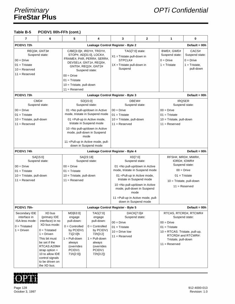
FireStar PlusPreliminary OPTi Confidential
PCIDV1 72h Leakage Control Register - Byte 2 Default = 00h
REQ3#, GNT3# Suspend state:
00 = Drive
01 = Tristate
10 = Reserved
11 = Reserved
C/BE[3:0]#, IRDY#, TRDY#, STOP#, AD[31:0], LOCK#,
FRAME#, PAR, PERR#, SERR#, DEVSEL#, GNT1#, REQ0#,
GNT0#, REQ2#, GNT2# Suspend state:
00 = Drive
01 = Tristate
10 = Tristate, pull-down
11 = Reserved
TAG[7:0] state:
X1 = Tristate pull-down in STPCLK#
1X = Tristate pull-down in Suspend
BWE#, GWE# Suspend state:
0 = Drive
1 = Tristate
CACS# Suspend state:
0 = Drive
1 = Tristate, pull-down
PCIDV1 73h Leakage Control Register - Byte 3 Default = 00h
CMD# Suspend state:
00 = Drive
01 = Tristate
10 = Tristate, pull-down
11 = Reserved
SD[15:0] Suspend state:
01 =No pull-up/down in Active mode, tristate in Suspend mode
01 =Pull-up in Active mode, tristate in Suspend mode
10 =No pull-up/down in Active mode, pull-down in Suspend
mode
11 =Pull-up in Active mode, pull-down in Suspend mode
DBEW# Suspend state:
00 = Drive
01 = Tristate
10 = Tristate, pull-down
11 = Reserved
IRQSER Suspend state:
00 = Drive
01 = Tristate
10 = Tristate, pull-down
11 = Reserved
PCIDV1 74h Leakage Control Register - Byte 4 Default = 00h
SA[15:0] Suspend state:
00 = Drive
01 = Tristate
10 = Tristate, pull-down
11 = Reserved
SA[23:18] Suspend state:
00 = Drive
01 = Tristate
10 = Tristate, pull-down
11 = Reserved
XD[7:0] Suspend state:
01 =No pull-up/down in Active mode, tristate in Suspend mode
01 =Pull-up in Active mode, tristate in Suspend mode
10 =No pull-up/down in Active mode, pull-down in Suspend
mode
11 =Pull-up in Active mode, pull-down in Suspend mode
RFSH#, MRD#, MWR#, IORD#, IOWR# Suspend state:
00 = Drive
01 = Tristate
10 = Tristate, pull-down
11 = Reserved
PCIDV1 75h- Leakage Control Register - Byte 5 Default = 00h
Secondary IDE interface in
ISA-less mode:
0 = Tristated1 = Driven
XD bus (primary IDE
interface) in no XD bus mode:
0 = Tristated1 = Driven
This bit must be set if the RTCAS:A20M# strap option = 10 to allow IDE control signals to be driven on the XD bus.
MD[63:0] engage
pull-down:
0 = Controlled by PCIDV1 71[2:0]h
1 = Pull-down always (overrides PCIDV1 71h[2:0])
TAG[7:0] engage
pull-down:
0 = Controlled by PCIDV1 72h[3:2]
1 = Pull-down always (overrides PCIDV1 72h[3:2])
DACK[7:0]# Suspend state:
00 = Drive
01 = Tristate
10 = Drive low
11 = Reserved
RTCAS, RTCRD#, RTCWR# Suspend state:
00 = Drive
01 = Tristate
10 = RTCAS: Tristate, pull-up,RTCRD# and RTCWR#: Tristate, pull-down
11 = Reserved
Table B-5 PCIDV1 00h-FFh (cont.)
7 6 5 4 3 2 1 0
Page 128 912-4000-013October 3, 1997 Revision: 1.0
OPTi®
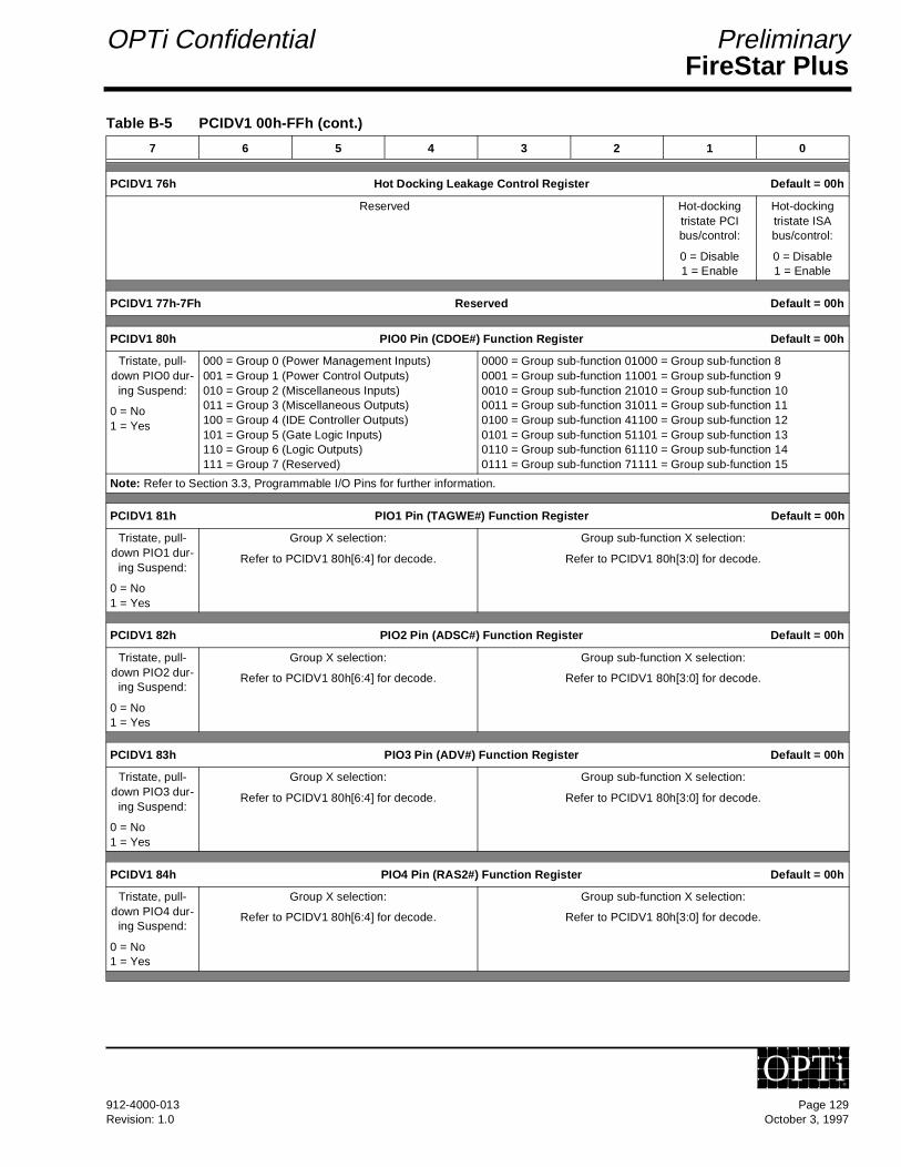
FireStar PlusOPTi Confidential Preliminary
PCIDV1 76h Hot Docking Leakage Control Register Default = 00h
Reserved Hot-docking tristate PCI bus/control:
0 = Disable1 = Enable
Hot-docking tristate ISA bus/control:
0 = Disable1 = Enable
PCIDV1 77h-7Fh Reserved Default = 00h
PCIDV1 80h PIO0 Pin (CDOE#) Function Register Default = 00h
Tristate, pull-down PIO0 dur-
ing Suspend:
0 = No1 = Yes
000 = Group 0 (Power Management Inputs)001 = Group 1 (Power Control Outputs)010 = Group 2 (Miscellaneous Inputs)011 = Group 3 (Miscellaneous Outputs)100 = Group 4 (IDE Controller Outputs)101 = Group 5 (Gate Logic Inputs)110 = Group 6 (Logic Outputs)111 = Group 7 (Reserved)
0000 = Group sub-function 01000 = Group sub-function 80001 = Group sub-function 11001 = Group sub-function 90010 = Group sub-function 21010 = Group sub-function 100011 = Group sub-function 31011 = Group sub-function 110100 = Group sub-function 41100 = Group sub-function 120101 = Group sub-function 51101 = Group sub-function 130110 = Group sub-function 61110 = Group sub-function 140111 = Group sub-function 71111 = Group sub-function 15
Note: Refer to Section 3.3, Programmable I/O Pins for further information.
PCIDV1 81h PIO1 Pin (TAGWE#) Function Register Default = 00h
Tristate, pull-down PIO1 dur-
ing Suspend:
0 = No1 = Yes
Group X selection:
Refer to PCIDV1 80h[6:4] for decode.
Group sub-function X selection:
Refer to PCIDV1 80h[3:0] for decode.
PCIDV1 82h PIO2 Pin (ADSC#) Function Register Default = 00h
Tristate, pull-down PIO2 dur-
ing Suspend:
0 = No1 = Yes
Group X selection:
Refer to PCIDV1 80h[6:4] for decode.
Group sub-function X selection:
Refer to PCIDV1 80h[3:0] for decode.
PCIDV1 83h PIO3 Pin (ADV#) Function Register Default = 00h
Tristate, pull-down PIO3 dur-
ing Suspend:
0 = No1 = Yes
Group X selection:
Refer to PCIDV1 80h[6:4] for decode.
Group sub-function X selection:
Refer to PCIDV1 80h[3:0] for decode.
PCIDV1 84h PIO4 Pin (RAS2#) Function Register Default = 00h
Tristate, pull-down PIO4 dur-
ing Suspend:
0 = No1 = Yes
Group X selection:
Refer to PCIDV1 80h[6:4] for decode.
Group sub-function X selection:
Refer to PCIDV1 80h[3:0] for decode.
Table B-5 PCIDV1 00h-FFh (cont.)
7 6 5 4 3 2 1 0
912-4000-013 Page 129Revision: 1.0 October 3, 1997
OPTi®

FireStar PlusPreliminary OPTi Confidential
PCIDV1 85h PIO5 Pin (RAS1#) Function Register Default = 00h
Tristate, pull-down PIO5 dur-
ing Suspend:
0 = No1 = Yes
Group X selection:
Refer to PCIDV1 80h[6:4] for decode.
Group sub-function X selection:
Refer to PCIDV1 80h[3:0] for decode.
PCIDV1 86h PIO6 Pin (CLKRUN#) Function Register Default = 00h
Tristate, pull-down PIO6 dur-
ing Suspend:
0 = No1 = Yes
Group X selection:
Refer to PCIDV1 80h[6:4] for decode.
Group sub-function X selection:
Refer to PCIDV1 80h[3:0] for decode.
PCIDV1 87h PIO7 Pin (REQ1#) Function Register Default = 00h
Tristate, pull-down PIO7 dur-
ing Suspend:
0 = No1 = Yes
Group X selection:
Refer to PCIDV1 80h[6:4] for decode.
Group sub-function X selection:
Refer to PCIDV1 80h[3:0] for decode.
PCIDV1 88h PIO8 Pin (REQ2#) Function Register Default = 00h
Tristate, pull-down PIO8 dur-
ing Suspend:
0 = No1 = Yes
Group X selection:
Refer to PCIDV1 80h[6:4] for decode.
Group sub-function X selection:
Refer to PCIDV1 80h[3:0] for decode.
PCIDV1 89h PIO9 Pin (DDRQ0) Function Register Default = 00h
Tristate, pull-down PIO9 dur-
ing Suspend:
0 = No1 = Yes
Group X selection:
Refer to PCIDV1 80h[6:4] for decode.
Group sub-function X selection:
Refer to PCIDV1 80h[3:0] for decode.
PCIDV1 8Ah PIO10 Pin (IRQ1) Function Register Default = 00h
Tristate, pull-down PIO10
during Suspend:
0 = No1 = Yes
Group X selection:
Refer to PCIDV1 80h[6:4] for decode.
Group sub-function X selection:
Refer to PCIDV1 80h[3:0] for decode.
PCIDV1 8Bh PIO11 Pin (IRQ8#) Function Register Default = 00h
Tristate, pull-down PIO11
during Suspend:
0 = No1 = Yes
Group X selection:
Refer to PCIDV1 80h[6:4] for decode.
Group sub-function X selection:
Refer to PCIDV1 80h[3:0] for decode.
Table B-5 PCIDV1 00h-FFh (cont.)
7 6 5 4 3 2 1 0
Page 130 912-4000-013October 3, 1997 Revision: 1.0
OPTi®

FireStar PlusOPTi Confidential Preliminary
PCIDV1 8Ch PIO12 Pin (IRQ12) Function Register Default = 00h
Tristate, pull-down PIO12
during Suspend:
0 = No1 = Yes
Group X selection:
Refer to PCIDV1 80h[6:4] for decode.
Group sub-function X selection:
Refer to PCIDV1 80h[3:0] for decode.
PCIDV1 8Dh PIO13 Pin (IRQ14) Function Register Default = 00h
Tristate, pull-down PIO13
during Suspend:
0 = No1 = Yes
Group X selection:
Refer to PCIDV1 80h[6:4] for decode.
Group sub-function X selection:
Refer to PCIDV1 80h[3:0] for decode.
PCIDV1 8Eh PIO14 Pin (SEL#/ATB#) Function Register Default = 00h
Tristate, pull-down PIO14
during Suspend:
0 = No1 = Yes
Group X selection:
Refer to PCIDV1 80h[6:4] for decode.
Group sub-function X selection:
Refer to PCIDV1 80h[3:0] for decode.
PCIDV1 8Fh PIO15 Pin (RSTDRV) Function Register Default = 00h
Tristate, pull-down PIO15
during Suspend:
0 = No1 = Yes
Group X selection:
Refer to PCIDV1 80h[6:4] for decode.
Group sub-function X selection:
Refer to PCIDV1 80h[3:0] for decode.
PCIDV1 90h PIO16 Pin (SA16) Function Register Default = 00h
Tristate, pull-down PIO16
during Suspend:
0 = No1 = Yes
Group X selection:
Refer to PCIDV1 80h[6:4] for decode.
Group sub-function X selection:
Refer to PCIDV1 80h[3:0] for decode.
PCIDV1 91h PIO17 Pin (SA17) Function Register Default = 00h
Tristate, pull-down PIO17
during Suspend:
0 = No1 = Yes
Group X selection:
Refer to PCIDV1 80h[6:4] for decode.
Group sub-function X selection:
Refer to PCIDV1 80h[3:0] for decode.
Table B-5 PCIDV1 00h-FFh (cont.)
7 6 5 4 3 2 1 0
912-4000-013 Page 131Revision: 1.0 October 3, 1997
OPTi®
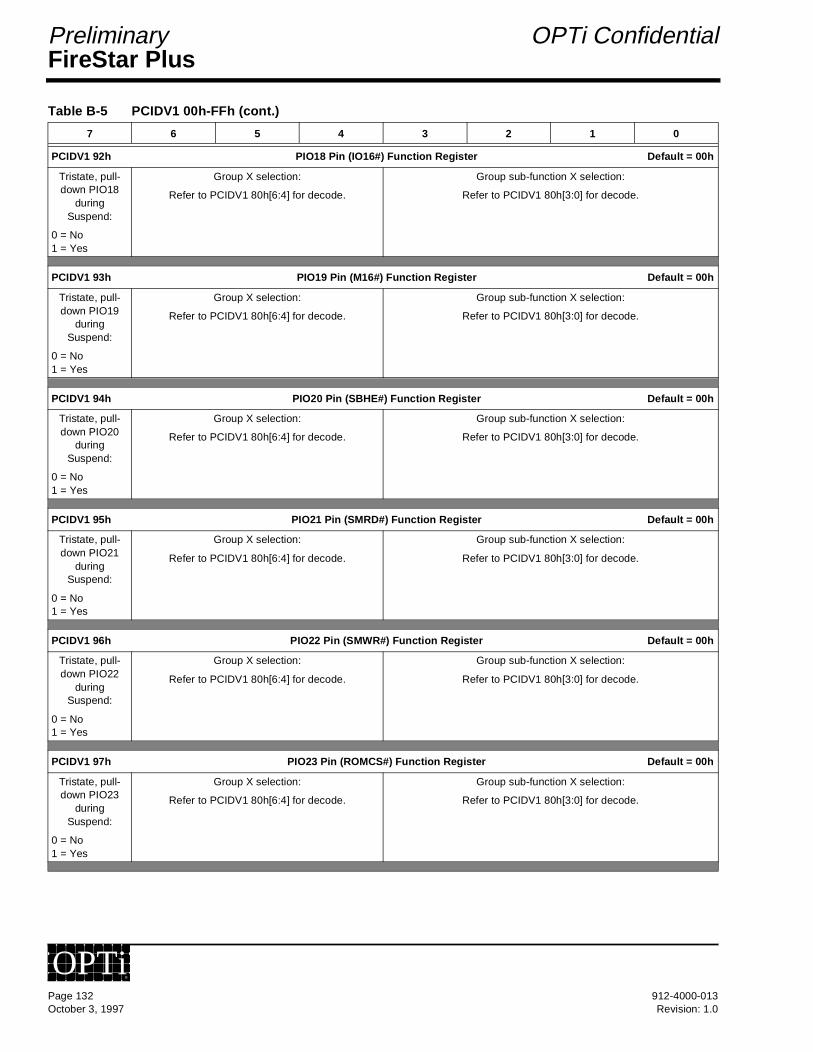
FireStar PlusPreliminary OPTi Confidential
PCIDV1 92h PIO18 Pin (IO16#) Function Register Default = 00h
Tristate, pull-down PIO18
during Suspend:
0 = No1 = Yes
Group X selection:
Refer to PCIDV1 80h[6:4] for decode.
Group sub-function X selection:
Refer to PCIDV1 80h[3:0] for decode.
PCIDV1 93h PIO19 Pin (M16#) Function Register Default = 00h
Tristate, pull-down PIO19
during Suspend:
0 = No1 = Yes
Group X selection:
Refer to PCIDV1 80h[6:4] for decode.
Group sub-function X selection:
Refer to PCIDV1 80h[3:0] for decode.
PCIDV1 94h PIO20 Pin (SBHE#) Function Register Default = 00h
Tristate, pull-down PIO20
during Suspend:
0 = No1 = Yes
Group X selection:
Refer to PCIDV1 80h[6:4] for decode.
Group sub-function X selection:
Refer to PCIDV1 80h[3:0] for decode.
PCIDV1 95h PIO21 Pin (SMRD#) Function Register Default = 00h
Tristate, pull-down PIO21
during Suspend:
0 = No1 = Yes
Group X selection:
Refer to PCIDV1 80h[6:4] for decode.
Group sub-function X selection:
Refer to PCIDV1 80h[3:0] for decode.
PCIDV1 96h PIO22 Pin (SMWR#) Function Register Default = 00h
Tristate, pull-down PIO22
during Suspend:
0 = No1 = Yes
Group X selection:
Refer to PCIDV1 80h[6:4] for decode.
Group sub-function X selection:
Refer to PCIDV1 80h[3:0] for decode.
PCIDV1 97h PIO23 Pin (ROMCS#) Function Register Default = 00h
Tristate, pull-down PIO23
during Suspend:
0 = No1 = Yes
Group X selection:
Refer to PCIDV1 80h[6:4] for decode.
Group sub-function X selection:
Refer to PCIDV1 80h[3:0] for decode.
Table B-5 PCIDV1 00h-FFh (cont.)
7 6 5 4 3 2 1 0
Page 132 912-4000-013October 3, 1997 Revision: 1.0
OPTi®
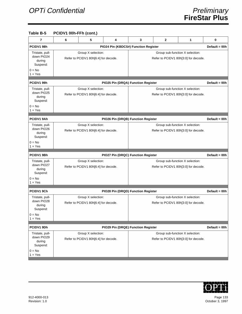
FireStar PlusOPTi Confidential Preliminary
PCIDV1 98h PIO24 Pin (KBDCS#) Function Register Default = 00h
Tristate, pull-down PIO24
during Suspend:
0 = No1 = Yes
Group X selection:
Refer to PCIDV1 80h[6:4] for decode.
Group sub-function X selection:
Refer to PCIDV1 80h[3:0] for decode.
PCIDV1 99h PIO25 Pin (DRQA) Function Register Default = 00h
Tristate, pull-down PIO25
during Suspend:
0 = No1 = Yes
Group X selection:
Refer to PCIDV1 80h[6:4] for decode.
Group sub-function X selection:
Refer to PCIDV1 80h[3:0] for decode.
PCIDV1 9Ah PIO26 Pin (DRQB) Function Register Default = 00h
Tristate, pull-down PIO26
during Suspend:
0 = No1 = Yes
Group X selection:
Refer to PCIDV1 80h[6:4] for decode.
Group sub-function X selection:
Refer to PCIDV1 80h[3:0] for decode.
PCIDV1 9Bh PIO27 Pin (DRQC) Function Register Default = 00h
Tristate, pull-down PIO27
during Suspend:
0 = No1 = Yes
Group X selection:
Refer to PCIDV1 80h[6:4] for decode.
Group sub-function X selection:
Refer to PCIDV1 80h[3:0] for decode.
PCIDV1 9Ch PIO28 Pin (DRQD) Function Register Default = 00h
Tristate, pull-down PIO28
during Suspend:
0 = No1 = Yes
Group X selection:
Refer to PCIDV1 80h[6:4] for decode.
Group sub-function X selection:
Refer to PCIDV1 80h[3:0] for decode.
PCIDV1 9Dh PIO29 Pin (DRQE) Function Register Default = 00h
Tristate, pull-down PIO29
during Suspend:
0 = No1 = Yes
Group X selection:
Refer to PCIDV1 80h[6:4] for decode.
Group sub-function X selection:
Refer to PCIDV1 80h[3:0] for decode.
Table B-5 PCIDV1 00h-FFh (cont.)
7 6 5 4 3 2 1 0
912-4000-013 Page 133Revision: 1.0 October 3, 1997
OPTi®
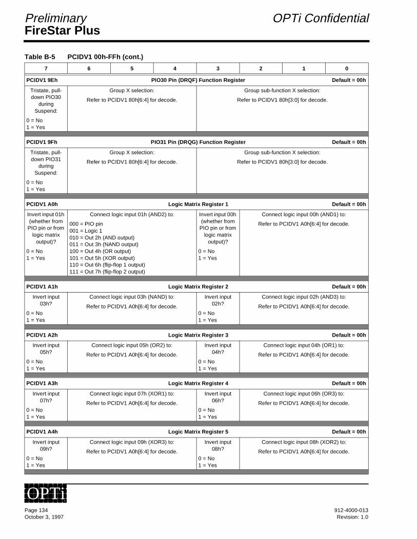
FireStar PlusPreliminary OPTi Confidential
PCIDV1 9Eh PIO30 Pin (DRQF) Function Register Default = 00h
Tristate, pull-down PIO30
during Suspend:
0 = No1 = Yes
Group X selection:
Refer to PCIDV1 80h[6:4] for decode.
Group sub-function X selection:
Refer to PCIDV1 80h[3:0] for decode.
PCIDV1 9Fh PIO31 Pin (DRQG) Function Register Default = 00h
Tristate, pull-down PIO31
during Suspend:
0 = No1 = Yes
Group X selection:
Refer to PCIDV1 80h[6:4] for decode.
Group sub-function X selection:
Refer to PCIDV1 80h[3:0] for decode.
PCIDV1 A0h Logic Matrix Register 1 Default = 00h
Invert input 01h (whether from
PIO pin or from logic matrix
output)?
0 = No1 = Yes
Connect logic input 01h (AND2) to:
000 = PIO pin001 = Logic 1010 = Out 2h (AND output)011 = Out 3h (NAND output)100 = Out 4h (OR output)101 = Out 5h (XOR output)110 = Out 6h (flip-flop 1 output)111 = Out 7h (flip-flop 2 output)
Invert input 00h (whether from
PIO pin or from logic matrix
output)?
0 = No1 = Yes
Connect logic input 00h (AND1) to:
Refer to PCIDV1 A0h[6:4] for decode.
PCIDV1 A1h Logic Matrix Register 2 Default = 00h
Invert input 03h?
0 = No1 = Yes
Connect logic input 03h (NAND) to:
Refer to PCIDV1 A0h[6:4] for decode.
Invert input 02h?
0 = No1 = Yes
Connect logic input 02h (AND3) to:
Refer to PCIDV1 A0h[6:4] for decode.
PCIDV1 A2h Logic Matrix Register 3 Default = 00h
Invert input 05h?
0 = No1 = Yes
Connect logic input 05h (OR2) to:
Refer to PCIDV1 A0h[6:4] for decode.
Invert input 04h?
0 = No1 = Yes
Connect logic input 04h (OR1) to:
Refer to PCIDV1 A0h[6:4] for decode.
PCIDV1 A3h Logic Matrix Register 4 Default = 00h
Invert input 07h?
0 = No1 = Yes
Connect logic input 07h (XOR1) to:
Refer to PCIDV1 A0h[6:4] for decode.
Invert input 06h?
0 = No1 = Yes
Connect logic input 06h (OR3) to:
Refer to PCIDV1 A0h[6:4] for decode.
PCIDV1 A4h Logic Matrix Register 5 Default = 00h
Invert input 09h?
0 = No1 = Yes
Connect logic input 09h (XOR3) to:
Refer to PCIDV1 A0h[6:4] for decode.
Invert input 08h?
0 = No1 = Yes
Connect logic input 08h (XOR2) to:
Refer to PCIDV1 A0h[6:4] for decode.
Table B-5 PCIDV1 00h-FFh (cont.)
7 6 5 4 3 2 1 0
Page 134 912-4000-013October 3, 1997 Revision: 1.0
OPTi®
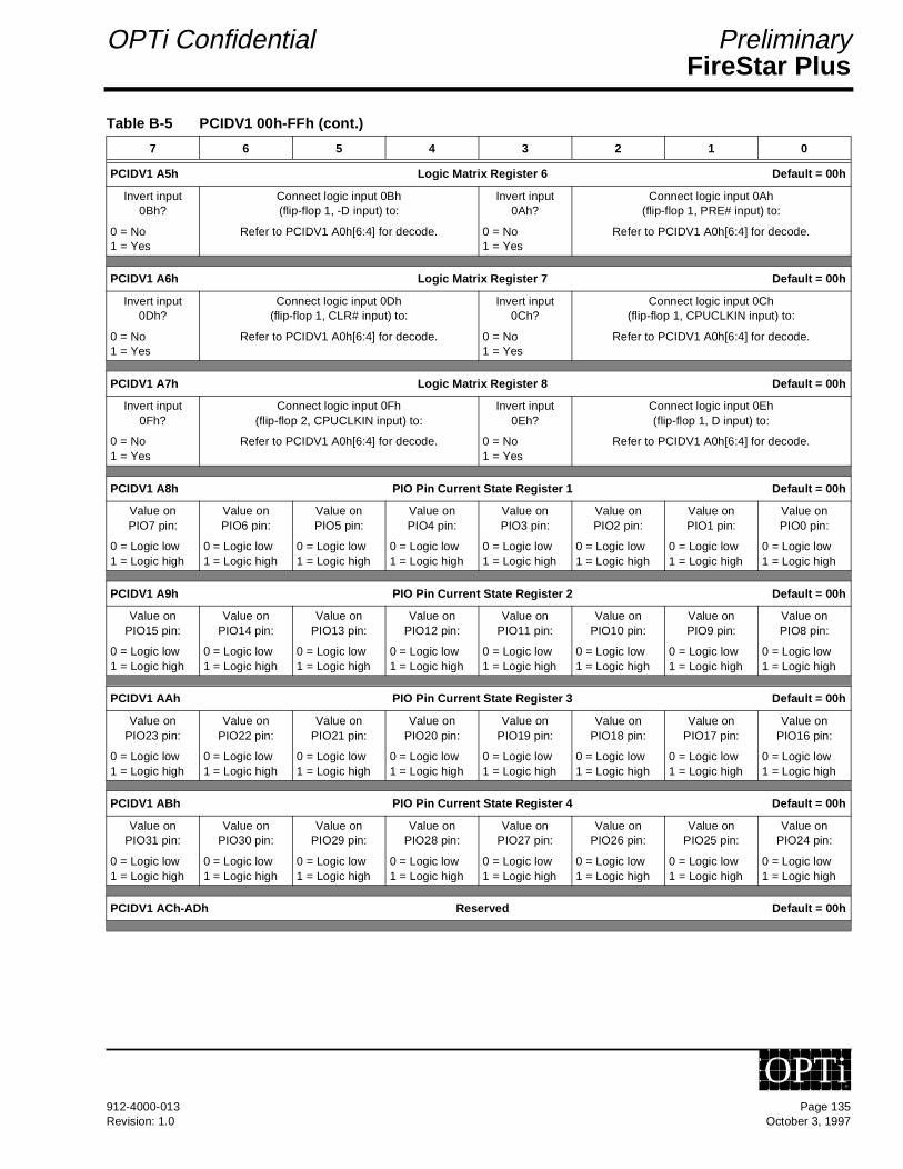
FireStar PlusOPTi Confidential Preliminary
PCIDV1 A5h Logic Matrix Register 6 Default = 00h
Invert input 0Bh?
0 = No1 = Yes
Connect logic input 0Bh (flip-flop 1, -D input) to:
Refer to PCIDV1 A0h[6:4] for decode.
Invert input 0Ah?
0 = No1 = Yes
Connect logic input 0Ah (flip-flop 1, PRE# input) to:
Refer to PCIDV1 A0h[6:4] for decode.
PCIDV1 A6h Logic Matrix Register 7 Default = 00h
Invert input 0Dh?
0 = No1 = Yes
Connect logic input 0Dh (flip-flop 1, CLR# input) to:
Refer to PCIDV1 A0h[6:4] for decode.
Invert input 0Ch?
0 = No1 = Yes
Connect logic input 0Ch (flip-flop 1, CPUCLKIN input) to:
Refer to PCIDV1 A0h[6:4] for decode.
PCIDV1 A7h Logic Matrix Register 8 Default = 00h
Invert input 0Fh?
0 = No1 = Yes
Connect logic input 0Fh (flip-flop 2, CPUCLKIN input) to:
Refer to PCIDV1 A0h[6:4] for decode.
Invert input 0Eh?
0 = No1 = Yes
Connect logic input 0Eh (flip-flop 1, D input) to:
Refer to PCIDV1 A0h[6:4] for decode.
PCIDV1 A8h PIO Pin Current State Register 1 Default = 00h
Value on PIO7 pin:
0 = Logic low1 = Logic high
Value on PIO6 pin:
0 = Logic low1 = Logic high
Value on PIO5 pin:
0 = Logic low1 = Logic high
Value on PIO4 pin:
0 = Logic low1 = Logic high
Value on PIO3 pin:
0 = Logic low1 = Logic high
Value on PIO2 pin:
0 = Logic low1 = Logic high
Value on PIO1 pin:
0 = Logic low1 = Logic high
Value on PIO0 pin:
0 = Logic low1 = Logic high
PCIDV1 A9h PIO Pin Current State Register 2 Default = 00h
Value on PIO15 pin:
0 = Logic low1 = Logic high
Value on PIO14 pin:
0 = Logic low1 = Logic high
Value on PIO13 pin:
0 = Logic low1 = Logic high
Value on PIO12 pin:
0 = Logic low1 = Logic high
Value on PIO11 pin:
0 = Logic low1 = Logic high
Value on PIO10 pin:
0 = Logic low1 = Logic high
Value on PIO9 pin:
0 = Logic low1 = Logic high
Value on PIO8 pin:
0 = Logic low1 = Logic high
PCIDV1 AAh PIO Pin Current State Register 3 Default = 00h
Value on PIO23 pin:
0 = Logic low1 = Logic high
Value on PIO22 pin:
0 = Logic low1 = Logic high
Value on PIO21 pin:
0 = Logic low1 = Logic high
Value on PIO20 pin:
0 = Logic low1 = Logic high
Value on PIO19 pin:
0 = Logic low1 = Logic high
Value on PIO18 pin:
0 = Logic low1 = Logic high
Value on PIO17 pin:
0 = Logic low1 = Logic high
Value on PIO16 pin:
0 = Logic low1 = Logic high
PCIDV1 ABh PIO Pin Current State Register 4 Default = 00h
Value on PIO31 pin:
0 = Logic low1 = Logic high
Value on PIO30 pin:
0 = Logic low1 = Logic high
Value on PIO29 pin:
0 = Logic low1 = Logic high
Value on PIO28 pin:
0 = Logic low1 = Logic high
Value on PIO27 pin:
0 = Logic low1 = Logic high
Value on PIO26 pin:
0 = Logic low1 = Logic high
Value on PIO25 pin:
0 = Logic low1 = Logic high
Value on PIO24 pin:
0 = Logic low1 = Logic high
PCIDV1 ACh-ADh Reserved Default = 00h
Table B-5 PCIDV1 00h-FFh (cont.)
7 6 5 4 3 2 1 0
912-4000-013 Page 135Revision: 1.0 October 3, 1997
OPTi®
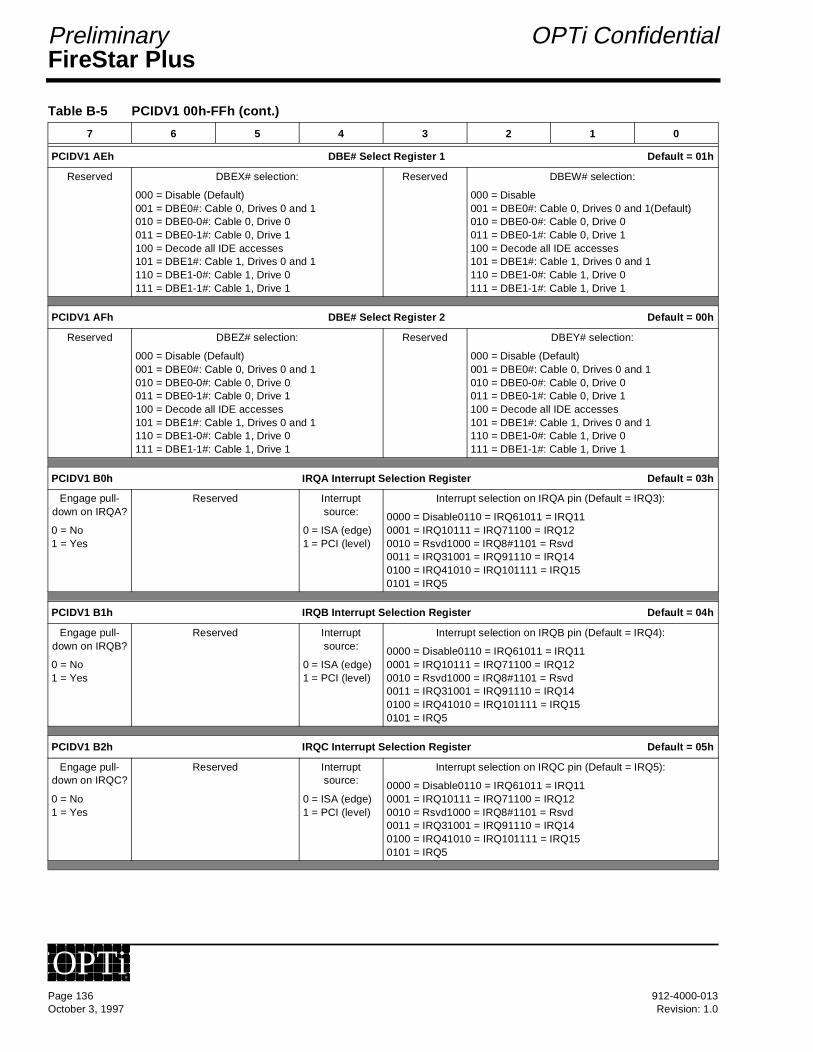
FireStar PlusPreliminary OPTi Confidential
PCIDV1 AEh DBE# Select Register 1 Default = 01h
Reserved DBEX# selection:
000 = Disable (Default)001 = DBE0#: Cable 0, Drives 0 and 1010 = DBE0-0#: Cable 0, Drive 0011 = DBE0-1#: Cable 0, Drive 1100 = Decode all IDE accesses101 = DBE1#: Cable 1, Drives 0 and 1110 = DBE1-0#: Cable 1, Drive 0111 = DBE1-1#: Cable 1, Drive 1
Reserved DBEW# selection:
000 = Disable 001 = DBE0#: Cable 0, Drives 0 and 1(Default)010 = DBE0-0#: Cable 0, Drive 0011 = DBE0-1#: Cable 0, Drive 1100 = Decode all IDE accesses101 = DBE1#: Cable 1, Drives 0 and 1110 = DBE1-0#: Cable 1, Drive 0111 = DBE1-1#: Cable 1, Drive 1
PCIDV1 AFh DBE# Select Register 2 Default = 00h
Reserved DBEZ# selection:
000 = Disable (Default)001 = DBE0#: Cable 0, Drives 0 and 1010 = DBE0-0#: Cable 0, Drive 0011 = DBE0-1#: Cable 0, Drive 1100 = Decode all IDE accesses101 = DBE1#: Cable 1, Drives 0 and 1110 = DBE1-0#: Cable 1, Drive 0111 = DBE1-1#: Cable 1, Drive 1
Reserved DBEY# selection:
000 = Disable (Default)001 = DBE0#: Cable 0, Drives 0 and 1010 = DBE0-0#: Cable 0, Drive 0011 = DBE0-1#: Cable 0, Drive 1100 = Decode all IDE accesses101 = DBE1#: Cable 1, Drives 0 and 1110 = DBE1-0#: Cable 1, Drive 0111 = DBE1-1#: Cable 1, Drive 1
PCIDV1 B0h IRQA Interrupt Selection Register Default = 03h
Engage pull-down on IRQA?
0 = No1 = Yes
Reserved Interrupt source:
0 = ISA (edge)1 = PCI (level)
Interrupt selection on IRQA pin (Default = IRQ3):
0000 = Disable0110 = IRQ61011 = IRQ110001 = IRQ10111 = IRQ71100 = IRQ120010 = Rsvd1000 = IRQ8#1101 = Rsvd0011 = IRQ31001 = IRQ91110 = IRQ140100 = IRQ41010 = IRQ101111 = IRQ150101 = IRQ5
PCIDV1 B1h IRQB Interrupt Selection Register Default = 04h
Engage pull-down on IRQB?
0 = No1 = Yes
Reserved Interrupt source:
0 = ISA (edge)1 = PCI (level)
Interrupt selection on IRQB pin (Default = IRQ4):
0000 = Disable0110 = IRQ61011 = IRQ110001 = IRQ10111 = IRQ71100 = IRQ120010 = Rsvd1000 = IRQ8#1101 = Rsvd0011 = IRQ31001 = IRQ91110 = IRQ140100 = IRQ41010 = IRQ101111 = IRQ150101 = IRQ5
PCIDV1 B2h IRQC Interrupt Selection Register Default = 05h
Engage pull-down on IRQC?
0 = No1 = Yes
Reserved Interrupt source:
0 = ISA (edge)1 = PCI (level)
Interrupt selection on IRQC pin (Default = IRQ5):
0000 = Disable0110 = IRQ61011 = IRQ110001 = IRQ10111 = IRQ71100 = IRQ120010 = Rsvd1000 = IRQ8#1101 = Rsvd0011 = IRQ31001 = IRQ91110 = IRQ140100 = IRQ41010 = IRQ101111 = IRQ150101 = IRQ5
Table B-5 PCIDV1 00h-FFh (cont.)
7 6 5 4 3 2 1 0
Page 136 912-4000-013October 3, 1997 Revision: 1.0
OPTi®
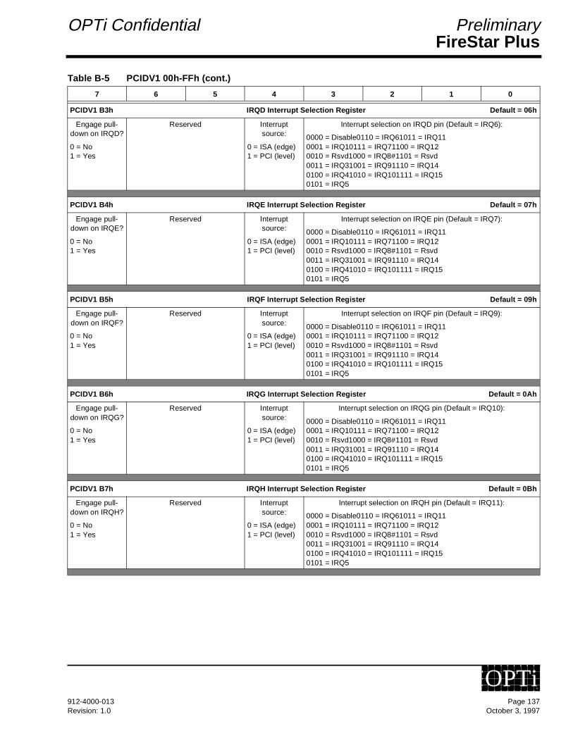
FireStar PlusOPTi Confidential Preliminary
PCIDV1 B3h IRQD Interrupt Selection Register Default = 06h
Engage pull-down on IRQD?
0 = No1 = Yes
Reserved Interrupt source:
0 = ISA (edge)1 = PCI (level)
Interrupt selection on IRQD pin (Default = IRQ6):
0000 = Disable0110 = IRQ61011 = IRQ110001 = IRQ10111 = IRQ71100 = IRQ120010 = Rsvd1000 = IRQ8#1101 = Rsvd0011 = IRQ31001 = IRQ91110 = IRQ140100 = IRQ41010 = IRQ101111 = IRQ150101 = IRQ5
PCIDV1 B4h IRQE Interrupt Selection Register Default = 07h
Engage pull-down on IRQE?
0 = No1 = Yes
Reserved Interrupt source:
0 = ISA (edge)1 = PCI (level)
Interrupt selection on IRQE pin (Default = IRQ7):
0000 = Disable0110 = IRQ61011 = IRQ110001 = IRQ10111 = IRQ71100 = IRQ120010 = Rsvd1000 = IRQ8#1101 = Rsvd0011 = IRQ31001 = IRQ91110 = IRQ140100 = IRQ41010 = IRQ101111 = IRQ150101 = IRQ5
PCIDV1 B5h IRQF Interrupt Selection Register Default = 09h
Engage pull-down on IRQF?
0 = No1 = Yes
Reserved Interrupt source:
0 = ISA (edge)1 = PCI (level)
Interrupt selection on IRQF pin (Default = IRQ9):
0000 = Disable0110 = IRQ61011 = IRQ110001 = IRQ10111 = IRQ71100 = IRQ120010 = Rsvd1000 = IRQ8#1101 = Rsvd0011 = IRQ31001 = IRQ91110 = IRQ140100 = IRQ41010 = IRQ101111 = IRQ150101 = IRQ5
PCIDV1 B6h IRQG Interrupt Selection Register Default = 0Ah
Engage pull-down on IRQG?
0 = No1 = Yes
Reserved Interrupt source:
0 = ISA (edge)1 = PCI (level)
Interrupt selection on IRQG pin (Default = IRQ10):
0000 = Disable0110 = IRQ61011 = IRQ110001 = IRQ10111 = IRQ71100 = IRQ120010 = Rsvd1000 = IRQ8#1101 = Rsvd0011 = IRQ31001 = IRQ91110 = IRQ140100 = IRQ41010 = IRQ101111 = IRQ150101 = IRQ5
PCIDV1 B7h IRQH Interrupt Selection Register Default = 0Bh
Engage pull-down on IRQH?
0 = No1 = Yes
Reserved Interrupt source:
0 = ISA (edge)1 = PCI (level)
Interrupt selection on IRQH pin (Default = IRQ11):
0000 = Disable0110 = IRQ61011 = IRQ110001 = IRQ10111 = IRQ71100 = IRQ120010 = Rsvd1000 = IRQ8#1101 = Rsvd0011 = IRQ31001 = IRQ91110 = IRQ140100 = IRQ41010 = IRQ101111 = IRQ150101 = IRQ5
Table B-5 PCIDV1 00h-FFh (cont.)
7 6 5 4 3 2 1 0
912-4000-013 Page 137Revision: 1.0 October 3, 1997
OPTi®
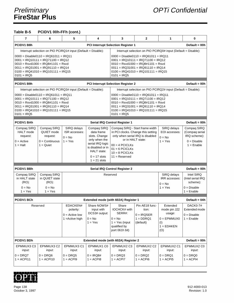
FireStar PlusPreliminary OPTi Confidential
PCIDV1 B8h PCI Interrupt Selection Register 1 Default = 00h
Interrupt selection on PIO PCIRQ1# input (Default = Disable):
0000 = Disable0110 = IRQ61011 = IRQ110001 = IRQ10111 = IRQ71100 = IRQ120010 = Rsvd1000 = IRQ8#1101 = Rsvd0011 = IRQ31001 = IRQ91110 = IRQ140100 = IRQ41010 = IRQ101111 = IRQ150101 = IRQ5
Interrupt selection on PIO PCIRQ0# input (Default = Disable):
0000 = Disable0110 = IRQ61011 = IRQ110001 = IRQ10111 = IRQ71100 = IRQ120010 = Rsvd1000 = IRQ8#1101 = Rsvd0011 = IRQ31001 = IRQ91110 = IRQ140100 = IRQ41010 = IRQ101111 = IRQ150101 = IRQ5
PCIDV1 B9h PCI Interrupt Selection Register 2 Default = 00h
Interrupt selection on PIO PCIRQ3# input (Default = Disable):
0000 = Disable0110 = IRQ61011 = IRQ110001 = IRQ10111 = IRQ71100 = IRQ120010 = Rsvd1000 = IRQ8#1101 = Rsvd0011 = IRQ31001 = IRQ91110 = IRQ140100 = IRQ41010 = IRQ101111 = IRQ150101 = IRQ5
Interrupt selection on PIO PCIRQ2# input (Default = Disable):
0000 = Disable0110 = IRQ61011 = IRQ110001 = IRQ10111 = IRQ71100 = IRQ120010 = Rsvd1000 = IRQ8#1101 = Rsvd0011 = IRQ31001 = IRQ91110 = IRQ140100 = IRQ41010 = IRQ101111 = IRQ150101 = IRQ5
PCIDV1 BAh Serial IRQ Control Register 1 Default = 00h
Compaq SIRQ HALT mode
request:
0 = Active1 = Halt
Compaq SIRQ QUIET mode
request:
0 = Continuous1 = Quiet
SIRQ delays ISR accesses:
0 = No1 = Yes
Compaq SIRQ data frame
slots. Change only when the
serial IRQ logic is disabled or in
HALT state:
0 = 17 slots1 = 21 slots
Compaq SIRQ - Start frame width in PCI clocks. Change this setting only when serial IRQ is disabled
or in HALT state:
00 = 4 PCICLKs01 = 6 PCICLKs10 = 8 PCICLKs11 = Reserved
SIRQ delays EOI accesses:
0 = No1 = Yes
Compaq SIRQ (Compaq serial IRQ scheme):
0 = Disable1 = Enable
PCIDV1 BBh Serial IRQ Control Register 2 Default = 00h
Compaq SIRQ in HALT state
(RO):
0 = No1 = Yes
Compaq SIRQ in QUIET state
(RO):
0 = No1 = Yes
Reserved SIRQ delays IRR accesses:
0 = No1 = Yes
Intel SIRQ (Intel serial IRQ
scheme):
0 = Disable1 = Enable
PCIDV1 BCh Extended mode (with 602A) Register 1 Default = 04h
Reserved EDACKEN# polarity:
0 = Active low1 =Active high
Share NOWS# input with
DCS3# output:
0 = No1 = Yes
Share IOCHCK# with
SERR#:
0 = No1 = Yes (input qualified by port 061h bit)
Pin AE18 func-tion:
0 = IRQSER1 = DDRQ1 (default)
Extended mode pin J22
usage:
0 = EPMMUX0 (I)1 = EDAKEN (O)
DACK0-7# Extended mode
0 = Disable1 = Enable
PCIDV1 BDh Extended mode (with 602A) Register 2 Default = 00h
EPMMUX3 C3 input:
0 = DRQ71 = ACPI11
EPMMUX3 C2 input:
0 = DRQ61 = ACPI10
EPMMUX3 C1 input:
0 = DRQ51 = ACPI9
EPMMUX1 C0 input:
0 = IRQ8#1 = ACPI8
EPMMUX2 C3 input:
0 = DRQ31 = ACPI7
EPMMUX2 C2 input:
0 = DRQ21 = ACPI6
EPMMUX2 C1 input:
0 = DRQ11 = ACPI5
EPMMUX2 C0 input:
0 = DRQ01 = ACPI4
Table B-5 PCIDV1 00h-FFh (cont.)
7 6 5 4 3 2 1 0
Page 138 912-4000-013October 3, 1997 Revision: 1.0
OPTi®
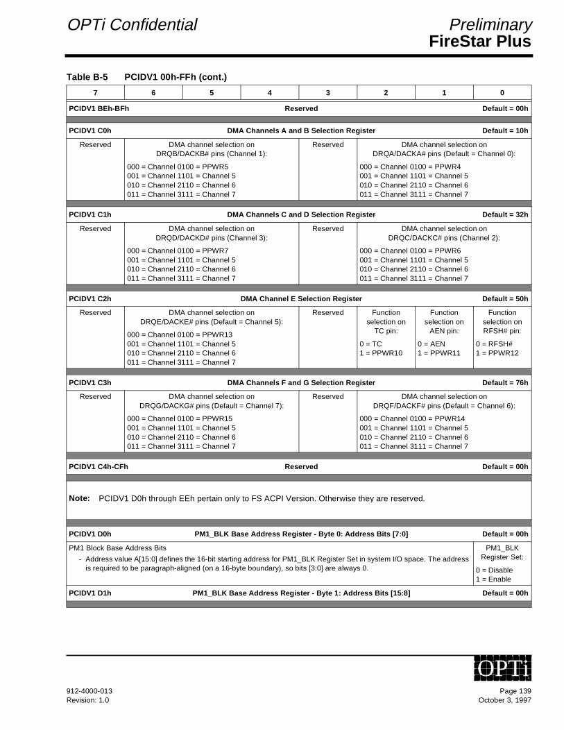
FireStar PlusOPTi Confidential Preliminary
PCIDV1 BEh-BFh Reserved Default = 00h
PCIDV1 C0h DMA Channels A and B Selection Register Default = 10h
Reserved DMA channel selection on DRQB/DACKB# pins (Channel 1):
000 = Channel 0100 = PPWR5001 = Channel 1101 = Channel 5010 = Channel 2110 = Channel 6011 = Channel 3111 = Channel 7
Reserved DMA channel selection on DRQA/DACKA# pins (Default = Channel 0):
000 = Channel 0100 = PPWR4001 = Channel 1101 = Channel 5010 = Channel 2110 = Channel 6011 = Channel 3111 = Channel 7
PCIDV1 C1h DMA Channels C and D Selection Register Default = 32h
Reserved DMA channel selection on DRQD/DACKD# pins (Channel 3):
000 = Channel 0100 = PPWR7001 = Channel 1101 = Channel 5010 = Channel 2110 = Channel 6011 = Channel 3111 = Channel 7
Reserved DMA channel selection on DRQC/DACKC# pins (Channel 2):
000 = Channel 0100 = PPWR6001 = Channel 1101 = Channel 5010 = Channel 2110 = Channel 6011 = Channel 3111 = Channel 7
PCIDV1 C2h DMA Channel E Selection Register Default = 50h
Reserved DMA channel selection on DRQE/DACKE# pins (Default = Channel 5):
000 = Channel 0100 = PPWR13001 = Channel 1101 = Channel 5010 = Channel 2110 = Channel 6011 = Channel 3111 = Channel 7
Reserved Function selection on
TC pin:
0 = TC1 = PPWR10
Function selection on
AEN pin:
0 = AEN1 = PPWR11
Function selection on RFSH# pin:
0 = RFSH#1 = PPWR12
PCIDV1 C3h DMA Channels F and G Selection Register Default = 76h
Reserved DMA channel selection on DRQG/DACKG# pins (Default = Channel 7):
000 = Channel 0100 = PPWR15001 = Channel 1101 = Channel 5010 = Channel 2110 = Channel 6011 = Channel 3111 = Channel 7
Reserved DMA channel selection on DRQF/DACKF# pins (Default = Channel 6):
000 = Channel 0100 = PPWR14001 = Channel 1101 = Channel 5010 = Channel 2110 = Channel 6011 = Channel 3111 = Channel 7
PCIDV1 C4h-CFh Reserved Default = 00h
Note: PCIDV1 D0h through EEh pertain only to FS ACPI Version. Otherwise they are reserved.
PCIDV1 D0h PM1_BLK Base Address Register - Byte 0: Address Bits [7:0] Default = 00h
PM1 Block Base Address Bits
- Address value A[15:0] defines the 16-bit starting address for PM1_BLK Register Set in system I/O space. The address is required to be paragraph-aligned (on a 16-byte boundary), so bits [3:0] are always 0.
PM1_BLK Register Set:
0 = Disable1 = Enable
PCIDV1 D1h PM1_BLK Base Address Register - Byte 1: Address Bits [15:8] Default = 00h
Table B-5 PCIDV1 00h-FFh (cont.)
7 6 5 4 3 2 1 0
912-4000-013 Page 139Revision: 1.0 October 3, 1997
OPTi®
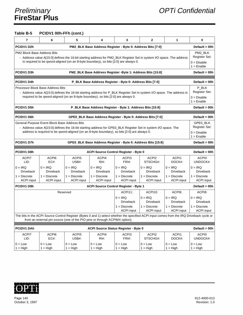
FireStar PlusPreliminary OPTi Confidential
PCIDV1 D2h PM2_BLK Base Address Register - Byte 0: Address Bits [7:0] Default = 00h
PM2 Block Base Address Bits
- Address value A[15:0] defines the 16-bit starting address for PM2_BLK Register Set in system I/O space. The address is required to be qword-aligned (on an 8-byte boundary), so bits [2:0] are always 0.
PM2_BLK Register Set:
0 = Disable1 = Enable
PCIDV1 D3h PM2_BLK Base Address Register -Byte 1: Address Bits [15:8] Default = 00h
PCIDV1 D4h P_BLK Base Address Register - Byte 0: Address Bits [7:0] Default = 00h
Processor Block Base Address Bits
- Address value A[15:0] defines the 16-bit starting address for P_BLK Register Set in system I/O space. The address is required to be qword-aligned (on an 8-byte boundary), so bits [2:0] are always 0.
P_BLK Register Set:
0 = Disable1 = Enable
PCIDV1 D5h P_BLK Base Address Register - Byte 1: Address Bits [15:8] Default = 00h
PCIDV1 D6h GPE0_BLK Base Address Register - Byte 0: Address Bits [7:0] Default = 00h
General Purpose Event Block Base Address Bits
- Address value A[15:0] defines the 16-bit starting address for GPE0_BLK Register Set in system I/O space. The address is required to be qword-aligned (on an 8-byte boundary), so bits [2:0] are always 0.
GPE0_BLK Register Set:
0 = Disable1 = Enable
PCIDV1 D7h GPE0_BLK Base Address Register - Byte 0: Address Bits [15:8] Default = 00h
PCIDV1 D8h ACPI Source Control Register - Byte 0 Default = 00h
ACPI7LID:
0 = IRQ Driveback
1 = Discrete ACPI input
ACPI6EC#:
0 = IRQ Driveback
1 = Discrete ACPI input
ACPI5USB#:
0 = IRQ Driveback
1 = Discrete ACPI input
ACPI4RI#:
0 = IRQ Driveback
1 = Discrete ACPI input
ACPI3FRI#:
0 = IRQ Driveback
1 = Discrete ACPI input
ACPI2STSCHG#:
0 = IRQ Driveback
1 = Discrete ACPI input
ACPI1DOCK#:
0 = IRQ Driveback
1 = Discrete ACPI input
ACPI0UNDOCK#:
0 = IRQ Driveback
1 = Discrete ACPI input
PCIDV1 D9h ACPI Source Control Register - Byte 1 Default = 00h
Reserved ACPI11:
0 = IRQ Driveback
1 = Discrete ACPI input
ACPI10:
0 = IRQ Driveback
1 = Discrete ACPI input
ACPI9:
0 = IRQ Driveback
1 = Discrete ACPI input
ACPI8:
0 = IRQ Driveback
1 = Discrete ACPI input
The bits in the ACPI Source Control Register (Bytes 0 and 1) select whether the specified ACPI input comes from the IRQ Driveback cycle or from an external pin source (one of the PIO pins or through ACPIMX option).
PCIDV1 DAh ACPI Source Status Register - Byte 0 Default = 00h
ACPI7LID:
0 = Low1 = High
ACPI6EC#:
0 = Low1 = High
ACPI5USB#:
0 = Low1 = High
ACPI4RI#:
0 = Low1 = High
ACPI3FRI#:
0 = Low1 = High
ACPI2STSCHG#:
0 = Low1 = High
ACPI1DOCK#:
0 = Low1 = High
ACPI0UNDOCK#:
0 = Low1 = High
Table B-5 PCIDV1 00h-FFh (cont.)
7 6 5 4 3 2 1 0
Page 140 912-4000-013October 3, 1997 Revision: 1.0
OPTi®

FireStar PlusOPTi Confidential Preliminary
PCIDV1 DBh ACPI Source Status Register - Byte 1 Default = 00h
Reserved ACPI11:
0 = Low1 = High
ACPI10:
0 = Low1 = High
ACPI9:
0 = Low1 = High
ACPI8:
0 = Low1 = High
The bits in the ACPI Source Status Register (Bytes 0 and 1) indicate the current state of the ACPI lines, either the discrete pins or the last IRQ Driveback value depending on the ACPI Source Control Register setting. This information may also be available elsewhere, since the IRQ Driveback values and PIO pin values can be read from other registers. However, this register provides a central means of reading signal state and is especially useful for signals such as LID (which generates an SCI, System Controller Interrupt, on both opening and closing events).
PCIDV1 DCh ACPI Event Resume Control Register - Byte 0 Default = 00h
ACPI7LID:
0 = Event will not cause Resume
1 = Event will cause Resume operation if system is in Suspend
ACPI6EC#:
0 = Event will not cause Resume
1 = Event will cause Resume operation if system is in Suspend
ACPI5USB#:
0 = Event will not cause Resume
1 = Event will cause Resume operation if system is in Suspend
ACPI4RI#:
0 = Event will not cause Resume
1 = Event will cause Resume operation if system is in Suspend
ACPI3FRI#:
0 = Event will not cause Resume
1 = Event will cause Resume operation if system is in Suspend
ACPI2STSCHG#:
0 = Event will not cause Resume
1 = Event will cause Resume operation if system is in Suspend
ACPI1DOCK#:
0 = Event will not cause Resume
1 = Event will cause Resume operation if system is in Suspend
ACPI0UNDOCK#:
0 = Event will not cause Resume
1 = Event will cause Resume operation if system is in Suspend
PCIDV1 DDh - ACPI Event Resume Control Register - Byte 1 Default = 00h
Reserved ACPI11:
0 = Event will not cause Resume
1 = Event will cause Resume operation if system is in Suspend
ACPI10:
0 = Event will not cause Resume
1 = Event will cause Resume operation if system is in Suspend
ACPI9:
0 = Event will not cause Resume
1 = Event will cause Resume operation if system is in Suspend
ACPI8:
0 = Event will not cause Resume
1 = Event will cause Resume operation if system is in Suspend
The bits in the ACPI Event Resume Control Register (Bytes 0 and 1) select whether the specified ACPI input can wake the system from its Suspend mode. Note that any PCI device that sends its information via the IRQ Driveback cycle will wake the system when it activates its CLKRUN# pin.
PCIDV1 DEh-DFh Reserved Default = 00h
Table B-5 PCIDV1 00h-FFh (cont.)
7 6 5 4 3 2 1 0
912-4000-013 Page 141Revision: 1.0 October 3, 1997
OPTi®
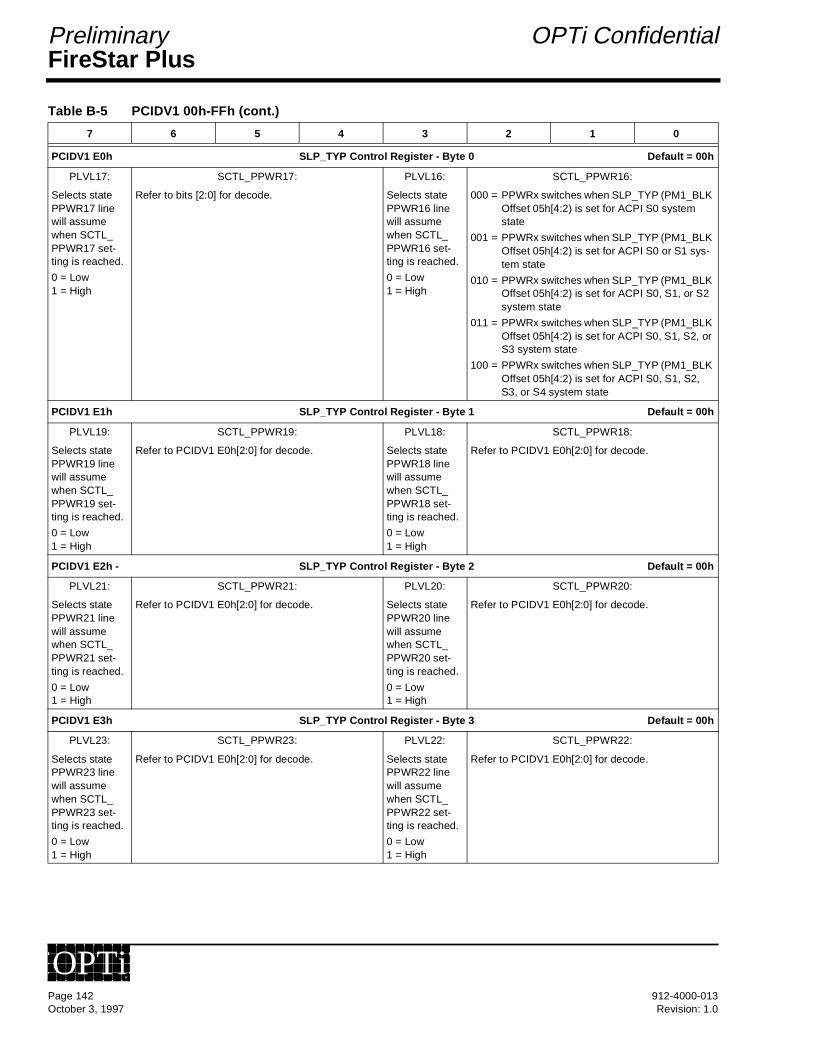
FireStar PlusPreliminary OPTi Confidential
PCIDV1 E0h SLP_TYP Control Register - Byte 0 Default = 00h
PLVL17:
Selects state PPWR17 line will assume when SCTL_PPWR17 set-ting is reached.
0 = Low1 = High
SCTL_PPWR17:
Refer to bits [2:0] for decode.
PLVL16:
Selects state PPWR16 line will assume when SCTL_PPWR16 set-ting is reached.
0 = Low1 = High
SCTL_PPWR16:
000 = PPWRx switches when SLP_TYP (PM1_BLK Offset 05h[4:2) is set for ACPI S0 system state
001 = PPWRx switches when SLP_TYP (PM1_BLK Offset 05h[4:2) is set for ACPI S0 or S1 sys-tem state
010 = PPWRx switches when SLP_TYP (PM1_BLK Offset 05h[4:2) is set for ACPI S0, S1, or S2 system state
011 = PPWRx switches when SLP_TYP (PM1_BLK Offset 05h[4:2) is set for ACPI S0, S1, S2, or S3 system state
100 = PPWRx switches when SLP_TYP (PM1_BLK Offset 05h[4:2) is set for ACPI S0, S1, S2, S3, or S4 system state
PCIDV1 E1h SLP_TYP Control Register - Byte 1 Default = 00h
PLVL19:
Selects state PPWR19 line will assume when SCTL_PPWR19 set-ting is reached.
0 = Low1 = High
SCTL_PPWR19:
Refer to PCIDV1 E0h[2:0] for decode.
PLVL18:
Selects state PPWR18 line will assume when SCTL_PPWR18 set-ting is reached.
0 = Low1 = High
SCTL_PPWR18:
Refer to PCIDV1 E0h[2:0] for decode.
PCIDV1 E2h - SLP_TYP Control Register - Byte 2 Default = 00h
PLVL21:
Selects state PPWR21 line will assume when SCTL_PPWR21 set-ting is reached.
0 = Low1 = High
SCTL_PPWR21:
Refer to PCIDV1 E0h[2:0] for decode.
PLVL20:
Selects state PPWR20 line will assume when SCTL_PPWR20 set-ting is reached.
0 = Low1 = High
SCTL_PPWR20:
Refer to PCIDV1 E0h[2:0] for decode.
PCIDV1 E3h SLP_TYP Control Register - Byte 3 Default = 00h
PLVL23:
Selects state PPWR23 line will assume when SCTL_PPWR23 set-ting is reached.
0 = Low1 = High
SCTL_PPWR23:
Refer to PCIDV1 E0h[2:0] for decode.
PLVL22:
Selects state PPWR22 line will assume when SCTL_PPWR22 set-ting is reached.
0 = Low1 = High
SCTL_PPWR22:
Refer to PCIDV1 E0h[2:0] for decode.
Table B-5 PCIDV1 00h-FFh (cont.)
7 6 5 4 3 2 1 0
Page 142 912-4000-013October 3, 1997 Revision: 1.0
OPTi®
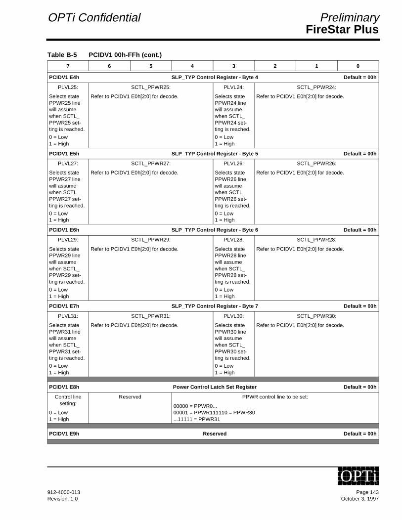
FireStar PlusOPTi Confidential Preliminary
PCIDV1 E4h SLP_TYP Control Register - Byte 4 Default = 00h
PLVL25:
Selects state PPWR25 line will assume when SCTL_PPWR25 set-ting is reached.
0 = Low1 = High
SCTL_PPWR25:
Refer to PCIDV1 E0h[2:0] for decode.
PLVL24:
Selects state PPWR24 line will assume when SCTL_PPWR24 set-ting is reached.
0 = Low1 = High
SCTL_PPWR24:
Refer to PCIDV1 E0h[2:0] for decode.
PCIDV1 E5h SLP_TYP Control Register - Byte 5 Default = 00h
PLVL27:
Selects state PPWR27 line will assume when SCTL_PPWR27 set-ting is reached.
0 = Low1 = High
SCTL_PPWR27:
Refer to PCIDV1 E0h[2:0] for decode.
PLVL26:
Selects state PPWR26 line will assume when SCTL_PPWR26 set-ting is reached.
0 = Low1 = High
SCTL_PPWR26:
Refer to PCIDV1 E0h[2:0] for decode.
PCIDV1 E6h SLP_TYP Control Register - Byte 6 Default = 00h
PLVL29:
Selects state PPWR29 line will assume when SCTL_PPWR29 set-ting is reached.
0 = Low1 = High
SCTL_PPWR29:
Refer to PCIDV1 E0h[2:0] for decode.
PLVL28:
Selects state PPWR28 line will assume when SCTL_PPWR28 set-ting is reached.
0 = Low1 = High
SCTL_PPWR28:
Refer to PCIDV1 E0h[2:0] for decode.
PCIDV1 E7h SLP_TYP Control Register - Byte 7 Default = 00h
PLVL31:
Selects state PPWR31 line will assume when SCTL_PPWR31 set-ting is reached.
0 = Low1 = High
SCTL_PPWR31:
Refer to PCIDV1 E0h[2:0] for decode.
PLVL30:
Selects state PPWR30 line will assume when SCTL_PPWR30 set-ting is reached.
0 = Low1 = High
SCTL_PPWR30:
Refer to PCIDV1 E0h[2:0] for decode.
PCIDV1 E8h Power Control Latch Set Register Default = 00h
Control line setting:
0 = Low1 = High
Reserved PPWR control line to be set:
00000 = PPWR0...00001 = PPWR111110 = PPWR30...11111 = PPWR31
PCIDV1 E9h Reserved Default = 00h
Table B-5 PCIDV1 00h-FFh (cont.)
7 6 5 4 3 2 1 0
912-4000-013 Page 143Revision: 1.0 October 3, 1997
OPTi®
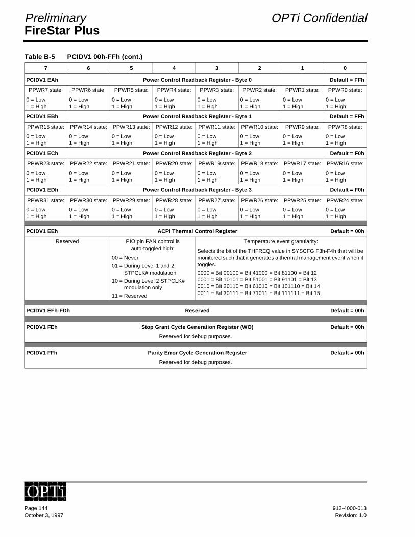
FireStar PlusPreliminary OPTi Confidential
PCIDV1 EAh Power Control Readback Register - Byte 0 Default = FFh
PPWR7 state:
0 = Low1 = High
PPWR6 state:
0 = Low1 = High
PPWR5 state:
0 = Low1 = High
PPWR4 state:
0 = Low1 = High
PPWR3 state:
0 = Low1 = High
PPWR2 state:
0 = Low1 = High
PPWR1 state:
0 = Low1 = High
PPWR0 state:
0 = Low1 = High
PCIDV1 EBh Power Control Readback Register - Byte 1 Default = FFh
PPWR15 state:
0 = Low1 = High
PPWR14 state:
0 = Low1 = High
PPWR13 state:
0 = Low1 = High
PPWR12 state:
0 = Low1 = High
PPWR11 state:
0 = Low1 = High
PPWR10 state:
0 = Low1 = High
PPWR9 state:
0 = Low1 = High
PPWR8 state:
0 = Low1 = High
PCIDV1 ECh Power Control Readback Register - Byte 2 Default = F0h
PPWR23 state:
0 = Low1 = High
PPWR22 state:
0 = Low1 = High
PPWR21 state:
0 = Low1 = High
PPWR20 state:
0 = Low1 = High
PPWR19 state:
0 = Low1 = High
PPWR18 state:
0 = Low1 = High
PPWR17 state:
0 = Low1 = High
PPWR16 state:
0 = Low1 = High
PCIDV1 EDh Power Control Readback Register - Byte 3 Default = F0h
PPWR31 state:
0 = Low1 = High
PPWR30 state:
0 = Low1 = High
PPWR29 state:
0 = Low1 = High
PPWR28 state:
0 = Low1 = High
PPWR27 state:
0 = Low1 = High
PPWR26 state:
0 = Low1 = High
PPWR25 state:
0 = Low1 = High
PPWR24 state:
0 = Low1 = High
PCIDV1 EEh ACPI Thermal Control Register Default = 00h
Reserved PIO pin FAN control is auto-toggled high:
00 = Never
01 = During Level 1 and 2 STPCLK# modulation
10 = During Level 2 STPCLK# modulation only
11 = Reserved
Temperature event granularity:
Selects the bit of the THFREQ value in SYSCFG F3h-F4h that will be monitored such that it generates a thermal management event when it toggles.
0000 = Bit 00100 = Bit 41000 = Bit 81100 = Bit 120001 = Bit 10101 = Bit 51001 = Bit 91101 = Bit 130010 = Bit 20110 = Bit 61010 = Bit 101110 = Bit 140011 = Bit 30111 = Bit 71011 = Bit 111111 = Bit 15
PCIDV1 EFh-FDh Reserved Default = 00h
PCIDV1 FEh Stop Grant Cycle Generation Register (WO) Default = 00h
Reserved for debug purposes.
PCIDV1 FFh Parity Error Cycle Generation Register Default = 00h
Reserved for debug purposes.
Table B-5 PCIDV1 00h-FFh (cont.)
7 6 5 4 3 2 1 0
Page 144 912-4000-013October 3, 1997 Revision: 1.0
OPTi®
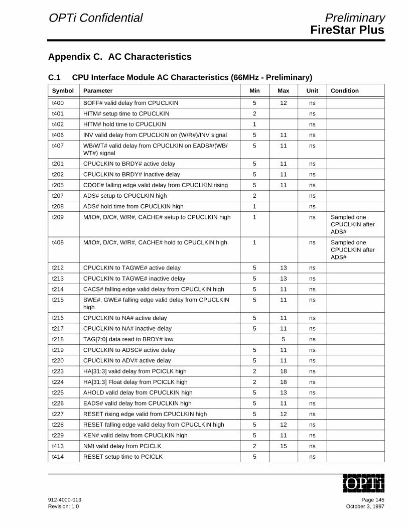
FireStar PlusOPTi Confidential Preliminary
Appendix C. AC Characteristics
C.1 CPU Interface Module AC Characteristics (66MHz - Preliminary)
Symbol Parameter Min Max Unit Condition
t400 BOFF# valid delay from CPUCLKIN 5 12 ns
t401 HITM# setup time to CPUCLKIN 2 ns
t402 HITM# hold time to CPUCLKIN 1 ns
t406 INV valid delay from CPUCLKIN on (W/R#)/INV signal 5 11 ns
t407 WB/WT# valid delay from CPUCLKIN on EADS#/(WB/WT#) signal
5 11 ns
t201 CPUCLKIN to BRDY# active delay 5 11 ns
t202 CPUCLKIN to BRDY# inactive delay 5 11 ns
t205 CDOE# falling edge valid delay from CPUCLKIN rising 5 11 ns
t207 ADS# setup to CPUCLKIN high 2 ns
t208 ADS# hold time from CPUCLKIN high 1 ns
t209 M/IO#, D/C#, W/R#, CACHE# setup to CPUCLKIN high 1 ns Sampled one CPUCLKIN after ADS#
t408 M/IO#, D/C#, W/R#, CACHE# hold to CPUCLKIN high 1 ns Sampled one CPUCLKIN after ADS#
t212 CPUCLKIN to TAGWE# active delay 5 13 ns
t213 CPUCLKIN to TAGWE# inactive delay 5 13 ns
t214 CACS# falling edge valid delay from CPUCLKIN high 5 11 ns
t215 BWE#, GWE# falling edge valid delay from CPUCLKIN high
5 11 ns
t216 CPUCLKIN to NA# active delay 5 11 ns
t217 CPUCLKIN to NA# inactive delay 5 11 ns
t218 TAG[7:0] data read to BRDY# low 5 ns
t219 CPUCLKIN to ADSC# active delay 5 11 ns
t220 CPUCLKIN to ADV# active delay 5 11 ns
t223 HA[31:3] valid delay from PCICLK high 2 18 ns
t224 HA[31:3] Float delay from PCICLK high 2 18 ns
t225 AHOLD valid delay from CPUCLKIN high 5 13 ns
t226 EADS# valid delay from CPUCLKIN high 5 11 ns
t227 RESET rising edge valid from CPUCLKIN high 5 12 ns
t228 RESET falling edge valid delay from CPUCLKIN high 5 12 ns
t229 KEN# valid delay from CPUCLKIN high 5 11 ns
t413 NMI valid delay from PCICLK 2 15 ns
t414 RESET setup time to PCICLK 5 ns
912-4000-013 Page 145Revision: 1.0 October 3, 1997
OPTi®
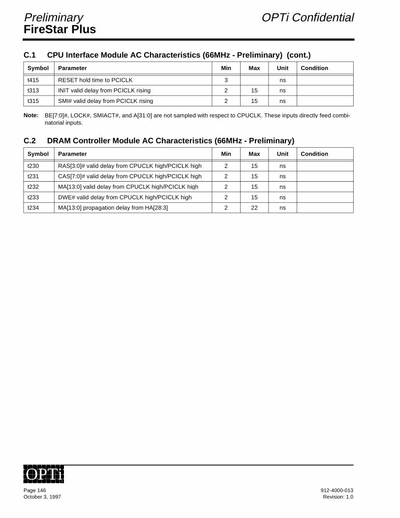
FireStar PlusPreliminary OPTi Confidential
Note: BE[7:0]#, LOCK#, SMIACT#, and A[31:0] are not sampled with respect to CPUCLK. These inputs directly feed combi-natorial inputs.
t415 RESET hold time to PCICLK 3 ns
t313 INIT valid delay from PCICLK rising 2 15 ns
t315 SMI# valid delay from PCICLK rising 2 15 ns
C.2 DRAM Controller Module AC Characteristics (66MHz - Preliminary)
Symbol Parameter Min Max Unit Condition
t230 RAS[3:0]# valid delay from CPUCLK high/PCICLK high 2 15 ns
t231 CAS[7:0]# valid delay from CPUCLK high/PCICLK high 2 15 ns
t232 MA[13:0] valid delay from CPUCLK high/PCICLK high 2 15 ns
t233 DWE# valid delay from CPUCLK high/PCICLK high 2 15 ns
t234 MA[13:0] propagation delay from HA[28:3] 2 22 ns
C.1 CPU Interface Module AC Characteristics (66MHz - Preliminary) (cont.)
Symbol Parameter Min Max Unit Condition
Page 146 912-4000-013October 3, 1997 Revision: 1.0
OPTi®
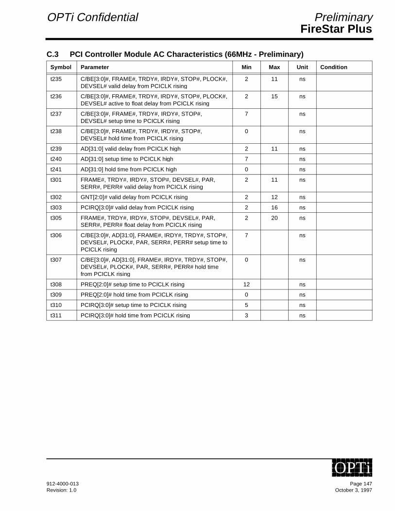
FireStar PlusOPTi Confidential Preliminary
C.3 PCI Controller Module AC Characteristics (66MHz - Preliminary)
Symbol Parameter Min Max Unit Condition
t235 C/BE[3:0]#, FRAME#, TRDY#, IRDY#, STOP#, PLOCK#, DEVSEL# valid delay from PCICLK rising
2 11 ns
t236 C/BE[3:0]#, FRAME#, TRDY#, IRDY#, STOP#, PLOCK#, DEVSEL# active to float delay from PCICLK rising
2 15 ns
t237 C/BE[3:0]#, FRAME#, TRDY#, IRDY#, STOP#, DEVSEL# setup time to PCICLK rising
7 ns
t238 C/BE[3:0]#, FRAME#, TRDY#, IRDY#, STOP#, DEVSEL# hold time from PCICLK rising
0 ns
t239 AD[31:0] valid delay from PCICLK high 2 11 ns
t240 AD[31:0] setup time to PCICLK high 7 ns
t241 AD[31:0] hold time from PCICLK high 0 ns
t301 FRAME#, TRDY#, IRDY#, STOP#, DEVSEL#, PAR, SERR#, PERR# valid delay from PCICLK rising
2 11 ns
t302 GNT[2:0]# valid delay from PCICLK rising 2 12 ns
t303 PCIRQ[3:0]# valid delay from PCICLK rising 2 16 ns
t305 FRAME#, TRDY#, IRDY#, STOP#, DEVSEL#, PAR, SERR#, PERR# float delay from PCICLK rising
2 20 ns
t306 C/BE[3:0]#, AD[31:0], FRAME#, IRDY#, TRDY#, STOP#, DEVSEL#, PLOCK#, PAR, SERR#, PERR# setup time to PCICLK rising
7 ns
t307 C/BE[3:0]#, AD[31:0], FRAME#, IRDY#, TRDY#, STOP#, DEVSEL#, PLOCK#, PAR, SERR#, PERR# hold time from PCICLK rising
0 ns
t308 PREQ[2:0]# setup time to PCICLK rising 12 ns
t309 PREQ[2:0]# hold time from PCICLK rising 0 ns
t310 PCIRQ[3:0]# setup time to PCICLK rising 5 ns
t311 PCIRQ[3:0]# hold time from PCICLK rising 3 ns
912-4000-013 Page 147Revision: 1.0 October 3, 1997
OPTi®

FireStar PlusPreliminary OPTi Confidential
Note: FERR# from the CPU is not sampled with respect to any clock. The input directly feeds combinatorial circuits.
C.4 ISA Controller Module AC Characteristics (66MHz - Preliminary)
Symbol Parameter Min Max Unit Condition
t314 ATCLK rising edge delay from PCICLK rising edge 5 20 ns
t416 A20M# valid delay from ATCLK 2 15 ns
t316 IOR#, IOW# high valid delay from ATCLK rising 15 ns
t317 MRD#, MWR#, SMRD#, SMWR# valid delay from ATCLK rising
15 ns
t318 BALE low valid delay from ATCLK rising 15 ns
t320 STPCLK# valid delay from ATCLK rising 15 ns
t321 RTCAS, RTCRD#, RTCWR#, ROMCS#/KBDCS# valid delay from ATCLK rising
15 ns
t322 BALE high valid delay from ATCLK falling 15 ns
t323 IOR#, IOW#, MRD#, MWR#, SMRD#, SMWR# low valid delay from ATCLK falling
15 ns
t324 PPWR0# valid delay from ATCLK falling 15 ns
t325 NOWS# setup time to ATCLK falling 0 ns
t326 NOWS# hold time from ATCLK falling 5 ns
t327 IOCHRDY setup time to ATCLK falling 5 ns
t328 IOCHRDY hold time from ATCLK falling 5 ns
Page 148 912-4000-013October 3, 1997 Revision: 1.0
OPTi®