Acid-Based Etching of Silicon Wafers: Mass-Transfer and ... · Chemical etching of silicon wafers...
13
176 Journal of The Electrochemical Society, 147 (1) 176-188 (2000) S0013-4651(99)02-063-7 CCC: $7.00 © The Electrochemical Society, Inc. Polished silicon wafers are prepared through various mechanical and chemical processes. First, the silicon single-crystal ingot is sliced into circular disks (wafers) by slicing followed by a flattening process called lapping that involves scrubbing the wafers using an abrasive slurry. 1 The mechanical damage induced during the previ- ous shaping processes is removed by etching which is the focus of this paper. Etching is followed by various unit operations such as polishing and cleaning before it is ready for device fabrication. Chemical etching of silicon wafers is accomplished by dipping the wafers in an etchant which is traditionally an acidic mixture of HNO 3 1 HF and a diluent or a caustic solution of KOH. Various studies in caustic crystallographic etching are reported. 2-4 However, this paper focuses on the transport and kinetic effects only on acid- based etches. Acid etching in HNO 3 1 HF mixture is reported to proceed with following global reactions 1 Si 1 4HNO 3 r SiO 2 1 4NO 2 1 2H 2 O [1] SiO 2 1 6HF r H 2 SiF 6 1 2H 2 O [2] Oxidants other than HNO 3 can also be used. The actual reaction mechanism is quite complicated and involves many elementary reactions. Hydrogen and different oxides of nitro- gen can evolve. Many rate equations for the dissolution of silicon wafer under different conditions have been proposed. 5-7 Sometimes, the identification of the rate-controlling step in a het- erogeneous process like this one (mass-transfer vs. reaction) becomes more critical than the knowledge of the actual chemistry in the design of an etcher, because a reaction-controlled etching requires a differ- ent design from a mass-transfer controlled etching to produce uni- formly etched silicon wafers. Schwartz and Robbins performed a series of experiments to quantify mass-transfer effects. 8 They etched wafers at different tem- peratures and correlated etch rates with the temperature using the Arrhenius expression. They attempted to identify the controlling step by the magnitude of the activation energy, a weak dependence of mass-transfer coefficient on temperature explained why the acti- vation energy for the mass-transfer influenced (not controlled) etch- ing was lower than that for the reaction influenced (not controlled) etching. This approach, although not very sophisticated, could be used to qualitatively recognize the rate-influencing step. Also, there is no quantitative evidence that kinetically controlled etching was achieved in these etching studies. Bogenschütz et al., however, claim that the viscosity of a liquid also can be expressed as an exponential function of temperature as follows 9 m ~ e 2Eam/KT [3] Since the viscosity is a transport property of the liquid, they claim that the temperature dependence of the viscosity is similar to the tempera- ture dependence of mass-transfer rates. The argument is not entirely valid because the mass-transfer coefficient is a function of many tem- perature dependent parameters other than viscosity. However, it seems that it is an accepted approach to recognize that the rate-controlling step is based on the magnitude of the activation energy. This approach is useful for qualitative understanding of the etching process. Robbins and Schwartz published a series of papers on acid etch- ing of silicon from 1958 to 1976. 8,10-12 They essentially established that for low HF and high HNO 3 concentrations, the etching process is greatly influenced by diffusion. Even for the low nitric acid con- centrations when the autocatalytic oxidation-reduction reaction influences the etching rate, mass-transfer effects are significant. 10,12 Their claim is supported by observations of Bogenschütz et al. and Klein and D’Stefan among many others. 9,13 Bogenschütz et al. showed that “activation energy” for mass-transfer controlled etching is comparable to the activation energy for viscosity. 9 Klein and D’Stefan observed a change in the etching rate with change in the mixing rate. 13 They observed a decrease in the dependence of the etching rate on the mixing rate with the increase in the HF concen- tration. This dependence was monotonic and linear. This means that the kinetic effects influence the etching process along with mass- transfer effects as the concentration of HF increases. Erk and Van- damme describe a process for chemical etching of silicon wafers where nitrogen bubbling is used for uniform mass-transfer effects. 14 Various earlier as well as recent studies indicate a very strong transport effect on etching. However, often, the attempt to explain these effects is based on various kinetic mechanisms. Schimmel compared performances of different acid etches in defect decora- tion. 15 He gave a qualitative kinetic explanation for defect decora- tion based on local rate differentials. The effect of stirring and, hence, transport was reported to have a significant effect on the sat- uration current density of an n-type Si electrode. 16 A qualitative rela- tionship between HF and/or oxidant concentration on the formation mechanism of stains in etching has been proposed by Nahm et al. and Schimmel and Elkind. 17,18 Fathauer et al. studied visible lumi- nescence from silicon wafers subjected to etches producing stains. 19 Gaffney and Chiou observed that by reducing the etching rate and moving into dissolution-limited regions, staining of silicon in nitric- hydrofluoric-acetic acid system is reduced. 20 Bauer et al. recognized Acid-Based Etching of Silicon Wafers: Mass-Transfer and Kinetic Effects Milind S. Kulkarni* ,z and Henry F. Erk MEMC Electronic Materials, Incorporated, Saint Peters, Missouri 63376-0008, USA A study to understand the transport and kinetic effects in three-phase, acid-based wet etching of silicon has been accomplished. Reactants overcome the liquid-phase mass-transfer resistance and the kinetic resistance to complete the reaction. The gaseous bub- bles formed by the reaction adhere to random sites on the surface and, thus, mask a fraction of the surface from the reactants. This bubble masking effect is modeled as the bubble transport resistance that acts in parallel with the liquid-phase mass-transfer resis- tance. These transport effects are lumped into an effective mass-transport resistance, which acts in series with the kinetic resistance. It is shown that the etched surface morphology is a function of the ratio of the effective mass-transport resistance to the kinetic resistance. A rough surface is a field of peaks and valleys. It is theorized that under mass-transfer influence, etch rates at peaks are higher than etch rates at valleys. Hence, the surface is chemically polished. It is shown that the polishing efficiency increases with increasing ratio of mass-transfer resistance to the kinetic resistance, reaches a maximum, and then decreases. Effects of mass-trans- fer and kinetics on the surface roughness and gloss are explained by both the developed phenomenological model and experimen- tal data. © 2000 The Electrochemical Society. S0013-4651(99)02-063-7. All rights reserved. Manuscript submitted February 16, 1999; revised manuscript received August 9, 1999. * Electrochemical Society Member. z E-mail: [email protected]
Transcript of Acid-Based Etching of Silicon Wafers: Mass-Transfer and ... · Chemical etching of silicon wafers...

176 Journal of The Electrochemical Society,147 (1) 176-188 (2000)S0013-4651(99)02-063-7 CCC: $7.00 © The Electrochemical Society, Inc.
Acid-Based Etching of Silicon Wafers: Mass-Transfer and Kinetic EffectsMilind S. Kulkarni* ,z and Henry F. Erk
MEMC Electronic Materials, Incorporated, Saint Peters, Missouri 63376-0008, USA
A study to understand the transport and kinetic effects in three-phase, acid-based wet etching of silicon has been accomplished.Reactants overcome the liquid-phase mass-transfer resistance and the kinetic resistance to complete the reaction. The gaseous bub-bles formed by the reaction adhere to random sites on the surface and, thus, mask a fraction of the surface from the reactants. Thisbubble masking effect is modeled as the bubble transport resistance that acts in parallel with the liquid-phase mass-transfer resis-tance. These transport effects are lumped into an effective mass-transport resistance, which acts in series with the kinetic resistance.It is shown that the etched surface morphology is a function of the ratio of the effective mass-transport resistance to the kineticresistance. A rough surface is a field of peaks and valleys. It is theorized that under mass-transfer influence, etch rates at peaks arehigher than etch rates at valleys. Hence, the surface is chemically polished. It is shown that the polishing efficiency increases withincreasing ratio of mass-transfer resistance to the kinetic resistance, reaches a maximum, and then decreases. Effects of mass-trans-fer and kinetics on the surface roughness and gloss are explained by both the developed phenomenological model and experimen-tal data.© 2000 The Electrochemical Society. S0013-4651(99)02-063-7. All rights reserved.
Manuscript submitted February 16, 1999; revised manuscript received August 9, 1999.
re as
hatera-tirelyem-eemsllingoach
tch-
sn-ion
ing
the theen- thatss-
Van-ferss.onglainmelora-ra-d,
sat-
tion
ns.and-
Polished silicon wafers are prepared through various mechanand chemical processes. First, the silicon single-crystal ingotsliced into circular disks (wafers) by slicing followed by a flatteninprocess called lapping that involves scrubbing the wafers usingabrasive slurry.1 The mechanical damage induced during the preous shaping processes is removed by etching which is the focuthis paper. Etching is followed by various unit operations suchpolishing and cleaning before it is ready for device fabrication.
Chemical etching of silicon wafers is accomplished by dippinthe wafers in an etchant which is traditionally an acidic mixture HNO3 1 HF and a diluent or a caustic solution of KOH. Varioustudies in caustic crystallographic etching are reported.2-4 However,this paper focuses on the transport and kinetic effects only on abased etches. Acid etching in HNO3 1 HF mixture is reported toproceed with following global reactions1
Si 1 4HNO3 r SiO2 1 4NO2 1 2H2O [1]
SiO2 1 6HF r H2SiF6 1 2H2O [2]
Oxidants other than HNO3 can also be used.The actual reaction mechanism is quite complicated and invol
many elementary reactions. Hydrogen and different oxides of nitgen can evolve. Many rate equations for the dissolution of silicwafer under different conditions have been proposed.5-7
Sometimes, the identification of the rate-controlling step in a herogeneous process like this one (mass-transfer vs.reaction) becomesmore critical than the knowledge of the actual chemistry in the desof an etcher, because a reaction-controlled etching requires a dient design from a mass-transfer controlled etching to produce formly etched silicon wafers.
Schwartz and Robbins performed a series of experimentsquantify mass-transfer effects.8 They etched wafers at different temperatures and correlated etch rates with the temperature usingArrhenius expression. They attempted to identify the controllistep by the magnitude of the activation energy, a weak dependeof mass-transfer coefficient on temperature explained why the avation energy for the mass-transfer influenced (not controlled) eting was lower than that for the reaction influenced (not controlleetching. This approach, although not very sophisticated, couldused to qualitatively recognize the rate-influencing step. Also, this no quantitative evidence that kinetically controlled etching wachieved in these etching studies.
* Electrochemical Society Member.z E-mail: [email protected]
ical isg anvi-s of as
gofs
cid-
vesro-on
et-
ignffer-uni-
to- the
ngncecti-ch-d)
beereas
Bogenschütz et al.,however, claim that the viscosity of a liquidalso can be expressed as an exponential function of temperatufollows9
m ~ e2Eam/KT [3]
Since the viscosity is a transport property of the liquid, they claim tthe temperature dependence of the viscosity is similar to the tempture dependence of mass-transfer rates. The argument is not envalid because the mass-transfer coefficient is a function of many tperature dependent parameters other than viscosity. However, it sthat it is an accepted approach to recognize that the rate-controstep is based on the magnitude of the activation energy. This appris useful for qualitative understanding of the etching process.
Robbins and Schwartz published a series of papers on acid eing of silicon from 1958 to 1976.8,10-12They essentially establishedthat for low HF and high HNO3 concentrations, the etching procesis greatly influenced by diffusion. Even for the low nitric acid cocentrations when the autocatalytic oxidation-reduction reactinfluences the etching rate, mass-transfer effects are significant.10,12
Their claim is supported by observations of Bogenschütz et al. andKlein and D’Stefan among many others.9,13 Bogenschütz et al.showed that “activation energy” for mass-transfer controlled etchis comparable to the activation energy for viscosity.9 Klein andD’Stefan observed a change in the etching rate with change inmixing rate.13 They observed a decrease in the dependence ofetching rate on the mixing rate with the increase in the HF conctration. This dependence was monotonic and linear. This meansthe kinetic effects influence the etching process along with matransfer effects as the concentration of HF increases. Erk and damme describe a process for chemical etching of silicon wawhere nitrogen bubbling is used for uniform mass-transfer effect14
Various earlier as well as recent studies indicate a very strtransport effect on etching. However, often, the attempt to expthese effects is based on various kinetic mechanisms. Schimcompared performances of different acid etches in defect dection.15 He gave a qualitative kinetic explanation for defect decotion based on local rate differentials. The effect of stirring anhence, transport was reported to have a significant effect on theuration current density of an n-type Si electrode.16A qualitative rela-tionship between HF and/or oxidant concentration on the formamechanism of stains in etching has been proposed by Nahm et al.and Schimmel and Elkind.17,18Fathauer et al. studied visible lumi-nescence from silicon wafers subjected to etches producing stai19
Gaffney and Chiou observed that by reducing the etching rate moving into dissolution-limited regions, staining of silicon in nitrichydrofluoric-acetic acid system is reduced.20 Bauer et al. recognized

Journal of The Electrochemical Society, 147 (1) 176-188 (2000) 177S0013-4651(99)02-063-7CCC:$7.00 © The Electrochemical Society, Inc.
the importance of fluid mechanics in acid etching.21 However, theygave no phenomenological explanation or quantification for the re-sults observed. Studies in acid etching of materials other than siliconusing HF have also reported the effect of HF concentration on thesurface morphology of the etched substrate.22 McAndrews andSukanek postulate that in the device etching with HF, air bubblesmay get trapped and cause surface irregularities.23 However, they donot consider the possibility of formation of bubbles by the etchingreaction or the resistance of these bubbles for the transport awayfrom the attached sites. Performance of etching is a strong functionof the equipment used as spray etching of silicon studied by Johnand Mcdonald seems to suggest.24 This leads to the conclusion thatmass-transfer effects are quite significant in acid etching, and manysurface characteristics cannot be simply explained by studyingchemical kinetics alone without taking transport effects into account.Thermodynamic dissolution windows for wet chemical processingof dilute aqueous Si-F system have been studied by Osseo-Asareet al., but, the effect of molecular transport to the reaction sites stillremained unanswered.25The shift in the controlling step, from kinet-ics to diffusion, in etching of thermal oxide by HF is discussed byMonk et al.26,27 However, this study discusses only dissolution ofthermal oxide by HF in a two-phase system. Monk et al. also re-viewed chemical reaction mechanism and kinetics for hydrofluoricacid etching of silicon dioxide.28 Kunii et al. studied wet etching ofdoped and nondoped silicon oxide films using buffered HF solu-tion.29They observed that etch rate showed linear dependence on HFconcentration at lower HF concentrations and nonlinear dependenceon HF concentration at higher HF concentrations. This shift wasexplained by the change in the dominant reactive species. Nonuni-formities in the oxide layer formed by boiling silicon wafers inHNO3 were reported by Aoyama et al.30 It is possible that nonuni-formities may influence subsequent processing such as etching.
Many of the observations discussed above often lead to contra-dictory conclusions because effects of mass-transport were not wellincorporated. The magnitude of the transport or diffusion effects isnot only a function of the speed of transport given by a transportcharacteristic time or transport resistance, but also a function of the
kinetic resistance or the kinetic characteristic time. The nature of theetched silicon wafer changes with a change in kinetic mechanism aswell as transport properties. There has been no methodical investi-gation to quantify the relative impact of mass-transport effects andkinetic effects in the etching process. In acid-based etching the con-trolling mechanism can impart its signature on the etched surface.Also, previous attempts to quantify kinetic and mass-transfer effectsin etching do not explain their effect on surface characteristics suchas roughness and gloss.
The purpose of this study is to present our experimental data andanalyze it using a novel phenomenological model for heterogeneousreactions. Data collected by us are consistent with the proposed phe-nomenological model for heterogeneous reactions and can explainvarious aspects of silicon surface characteristics. Since the proposedmodel explains different characteristics of the etched silicon wafersurface that earlier studies did not explain, there is a need for report-ing this data and analysis in the public literature.
Phenomenological Model: Two-Phase System
The etching process itself typically involves the following steps(Fig. 1a):(i ) transport of the reactants from the bulk solution to thewafer surface, (ii ) effective reaction(s) on the wafer surface, and (ii i )transport of products from the wafer surface to the bulk solution.
Reactants pass through a stagnant liquid film, which offers afinite resistance for mass-transfer before reactants reach the surfaceof the wafer. Products also pass through the mass-transfer film(henceforward, the term film refers to mass-transfer film unlessspecified otherwise). Hence, the reaction and physical transport ofreagents occur as steps in series. The finite rate of chemical kineticsprovides a finite kinetic resistance that acts in series with the mass-transfer resistance (Fig. 1a and b). When the mass-transfer and kinet-ic (reactive) resistances are comparable in magnitude, both kineticsand mass-transfer affect the rate of etching. However, when the dif-ference in the kinetic and mass-transfer resistances is appreciable,the step with higher resistance controls the rate of acid etching. Thephenomenological model shown in Fig. 1a and b is applicable to anytypical solid-liquid system.
Figure 1. (a) A schematic representation of the mass-transfer resistance in ageneric heterogeneous reaction system. (b) A phenomenological representa-tion of the kinetic and mass-transfer resistances in a generic heterogeneousreaction system. (c) A phenomenological representation of the concentrationboundary layer for the key reactant.

178 Journal of The Electrochemical Society, 147 (1) 176-188 (2000)S0013-4651(99)02-063-7 CCC:$7.00 © The Electrochemical Society, Inc.
Kinetic (reactive) and transport resistances.—The two-phasephenomenological model proposed is shown in Fig. 1a and b. Afinite mass-transfer resistance causes a drop in concentration of aspecies from the bulk value (Cb,i) to the solid-liquid interface value(Cf,i), and this drop is proportional to the mass-transfer resistance.According the classical mass-transfer theory,31,32 the rate of trans-port across the mass-transfer film is given by
rm,i 5 km,i(Cb,i 2 Cf,i) [4a]
[4b]
where mass-transfer rates (rm,i) are defined per cross-sectional areafor transport for any given species i. All terms in equations aredefined in the List of Symbols section. The driving force for themass-transport is the concentration difference across the mass-trans-fer film, and the resistance to the transport is given by the inverse ofmass-transfer coefficient.
The effective rate of reaction that incorporates adsorption-desorp-tion-diffusion effects in the silicon wafer at the interface is given by
(rr,i) 5 fr(T, Cf,i, Cf,j...) [5]
As an initial approximation, the effect of thermal boundary layer canbe neglected; however, analysis of the model does not change if thethermal boundary layer effects are appreciable. Kinetic resistancefor systems following simple kinetics is generally defined as a sys-tem constant.31 Nonetheless,in this paper we extend this analysisand define a nonlinear kinetic resistance that varies as a function ofinterfacial species concentration
[6]
Using Eq. 6,Eq. 5 can be rewritten as
where reaction rates for any given species i (rr,i) are defined per unitarea where reaction takes place.
At steady state, at any given location, reaction rates are equal tomass-transfer rates (rr,i 5 rm,i). Thus, for any given system,and agiven species,the kinetic and mass-transport resistances can bequantified and overall resistance is estimated as
implies Ro,i 5 Rm,i 1 Rr,i [7]
Figure 1c shows the schematic picture of the proposed model.
Characteristic times.—The speed of a process is inversely pro-portional to its characteristic time. The speed of a process is alsoinversely proportional to the resistance of the process. Hence, char-acteristic time and the resistance of a given process are related toeach other. For example, the resistances defined in Eq. 7 have unitsof seconds per meter. This means that the product of mass-transferresistance with a characteristic length scale such as mass-transferfilm thickness represents a characteristic time for mass-transfer.Similarly, the product of kinetic (reactive) resistance and a reactionlength scale such as equivalent reaction film thickness represents areaction characteristic time. Thus,for a special case when both reac-tion and mass-transfer length scales are identical (we can use thick-ness of either mass-transfer film or reactive film as the commonlength scale, provided both are of the same order of magnitude) the
rDF
R
C
R
C C
R
C
Rio,i
o,i
b,i
o,i
b,i f,i
m,i
f,i
r,i5 5
25
25
2( ) ( ) ( )0 0
( )( )
( , , ...)r
C
f T C C
C
DF
Rr,if,i
r f,i f, j
f,i
r,i
r,i5
25
01
( )( , , ...)
Rf T C C
C
r,ir f,i f, j
f,i
51
rC C
k
DF
Rm,ib,i f,i
m,i
m,i
m,i1
52
5( )
overall characteristic time of the process is given by summation ofthe characteristic kinetic time and characteristic transport time.Thus,as shown in Eq. 8,the resistance is a measure of the charac-teristic time
tm,i 5 dm,i 3 Rm,i and tr,i 5 dr,i 3 Rr,i [8]
Application of resistances.—The influence of transport and kin-etics on a system can be quantified by the ratio of mass-transportresistance to the kinetic resistance. If this ratio is greater than thecritical minimum value (that is specific to a system) the system ismass-transport influenced. The system is kinetically controlled whenthis ratio is below its critical value
and[9]
Thus the system is either controlled by the dominant resistance orinfluenced by both when neither of the resistances is negligible.
One goal of etching is to reduce the surface roughness. Rough-ness is a measure of nonuniformity of the surface represented as afield of peaks and valleys (Fig. 2) and is defined as
[10]
where f is the length averaged roughness. Note that l is not a peri-odic function of x as Fig. 2 indicates for simplicity. Roughness candecrease only if the rate of removal (etching) at peaks (rp,i) is greaterthan the rate of removal at valleys (rv,i) such that
[11]
where, js2l is the conversion factor that converts rates of consump-tion of species i per unit area, (r i) to removal rates based on thedecrease in thickness of silicon (rl ). Based on the magnitude ofmass-transport and kinetic resistances three cases can be studied.
Kinetically controlled etching.—As schematically explained in Fig.3a, for acid-based etching, in the absence of a mass-transfer film,rates of removal at valleys and peaks are comparable (rlp , rlv). Thisis also the case when the mass-transfer film thickness is very low(Fig. 3b). This happens when the ratio of resistances is below thecritical minimum value. Hence, kinetically controlled etching doesnot decrease roughness.
Mass-transfer influenced etching.—Mass-transfer influenced etch-ing improves the surface roughness and gloss. Figure 3c explains theeffect of mass-transfer film on the acid-based etching. The mass-transfer resistance is directly proportional to the thickness of thestagnant film. As shown in Fig. 3c, the mass-transfer resistance at the
dh
dtr r rl rl5 2 2 5 2 22js l p,i v,i p v( ) ( )
f
l
5 0
0
L
L
dx
dx
∫∫
R
R
R
Rm,i
r,i
m,i
r,iimplies kinetically controlled<
min
R
R
R
Rm,i
r,i
m,i
r,iimplies mass-transport influenced>
min
Figure 2. A schematic representation of roughness.

Journal of The Electrochemical Society, 147 (1) 176-188 (2000) 179S0013-4651(99)02-063-7CCC:$7.00 © The Electrochemical Society, Inc.
peaks is lower than that at valleys as a result of varying mass-trans-fer film thickness. Assuming that the kinetic resistance does nodecrease significantly from peaks to valleys, the overall resistance islower at peaks,and hence, removal rates at peaks are higher. As a re-
Figure 3. (a) A schematic speculation about a kinetically controlled etchingprocess. (b) A schematic view of insufficient mass-transfer effects on theetching process. (c). A schematic view of sufficient mass-transfer effects onthe etching process.
tsult of preferential etching at peaks,reduction in roughness isobserved. The ratio of etching rates at valleys and peaks is given by
[12]
Excessive mass-transfer controlled etching.—If the mass-transferfilm thickness is very low, the kinetic effects become stronger andetching tends to be kinetically controlled. If the mass-transfer film isvery thick, although mass-transport effects are predominant,the rel-ative difference between the film thickness at peaks and valleysdecreases as the total film thickness increases,i.e.
when
then
[13]
where [Rm,i/Rr,i]max is the critical excessive (maximum) resistanceratio and is specific to a system. Thus,simply increasing mass-trans-port resistance does not decrease the roughness. There is an opti-mum thickness of the mass-transfer film for each process. This opti-mum level is obtained when difference between etching rates atpeaks and valleys reaches the maximum.
Quantification of polishing efficiency.—Instantaneous polishingefficiency is defined as the ratio of actual rate of polishing to themaximum possible rate of polishing, i.e., it is equal to the ratio ofdifference between the etching rates at peaks and valleys to the etch-ing rate only at peaks
[14a]
The average polishing efficiency is the integral average of the instan-taneous polishing efficiency and is calculated as follows
[14b]
Thus,the average polishing efficiency is a function of surface kinet-ics and mass transport. For simple case of a first order kinetics and a
5
2
h
h
h
h
rl rl
rldh
dh
1
2
1
2
∫∫
p v
p
h
h
pol,avg
pol,instmax
5 5
2 2h
h
h
h
h
h
h
h
dh
dh
dh
dt
dh
dtdh
dh
1
2
1
2
1
2
1
2
∫∫
∫∫
5 2
1
1
1
1R
R
R
R
R
RR
R
R
R
m,p,i
m,v,i
r,p,i
r,v,i
m,p,i
r,p,i
m,p,i
m,v,i
m,p,i
r,v,i
hpol,inst
max
p v
p5
2
2
52
dh
dtdh
dt
rl rl
rl
limd dm,p,i, m,v,i
m,i
r,i
m,i
r,i max→∞
>
R
R
R
R
lim limd d d dm,p,i, m,v,i m,p,i, m,v,i
m,p,i
m,v,i
v,i
p,iimplies
→∞ →∞
R
R
r
r5 51 1
also that impliesm,p,i
m,v,i
v
p
R
R
rl
rl< <1 1
r
r
rl
rl
R
R
R
R
R
RR
R
R
R
v,i
p,i
v
p
m,p,i
m,v,i
r,p,i
r,v,i
m,p,i
r,p,i
m,p,i
m,v,i
m,p,i
r,v,i
5 5
1
1
1
1
<

180 Journal of The Electrochemical Society, 147 (1) 176-188 (2000)S0013-4651(99)02-063-7 CCC:$7.00 © The Electrochemical Society, Inc.
fixed mass-transfer film thickness,the average polishing efficiency toachieve a completely flat surface is derived by solving Eq.14b as
[15]
However, numerical estimation of polishing efficiency may becomenecessary for a more complex etching kinetics.
Thus,the mass-transfer film must be thick enough such that theratio of mass-transfer resistance to kinetic resistance must be abovethe critical minimum resistance ratio to ensure sufficient mass-trans-fer influence; also,the mass-transfer film must be thin enough suchthat the ratio of rate of etching at peaks to that at valleys is greaterthan unity. The dependence of polishing efficiency on the ratios ofthese resistances is schematically shown in Fig. 4. The polishingefficiency gradually increases with increasing ratio of mass-transferresistance to kinetic resistance, reaches a maximum value, and thenasymptotically approaches zero. Change in roughness to removal(2DF/DY) ratio is higher for a higher polishing efficiency.
Phenomenological Model: Three-Phase SystemAcid etching of silicon wafers is greatly influenced by gaseous
products. In the phenomenological model presented in the previoussection,the effect of gaseous products on the etching rate was notaddressed. Macromodeling of etching must incorporate (i ) transportof the reactants in the liquid phase from the bulk solution to thewafer surface, (ii ) effective reaction(s) on the wafer surface to pro-duce products in both liquid and gas phase, (ii i ) detachment ofgaseous products (bubbles) from the silicon surface, and (iv) trans-port of the gaseous products (bubbles) to the bulk phase.
NOx and hydrogen are generated by the etching reaction. Thesegases form bubbles that adhere to the silicon surface for a finite peri-od of time before they are dislodged. The etching reaction cannottake place on the sites masked by bubbles. Since the effective localthickness of the mass-transfer film is also affected by the dislodgedbubbles moving in this film, the rate of etching is affected by dis-lodged bubbles as well. The masking effect of bubbles influences theoverall rate of etching and also affects the surface morphology. How-ever, the bubble masking effect could be partially reduced by reduc-tion in mass-transfer resistance resulting from the mixing caused by
hd
dpol,avgm,v,i
r,i
m,v,i
m,v,i
2 1
for and5
1
$ 5
h
R
R
h h
1
1 2 0
,
Figure 4. Dependence of polishing efficiency on the ratio of mass-transferresistance to the kinetic resistance.
the detached bubbles in the mass-transfer film (autoreduction ofbubble masking).
Figure 5a shows a schematic of the silicon surface at any time dur-ing an etching process. The wafer surface is randomly covered by thebubbles produced by the reaction. Thus,at any instant,a fraction ofthe silicon wafer surface is masked by the bubbles and the rest is cov-ered by the liquid mass-transfer film. A site on the wafer surface israndomly occupied by gas and liquid alternately. This three-phasesystem is modeled as shown in Fig. 5b. The energy required to detacha bubble from the silicon surface depends on the surface tension,vis-cosity, density, and the surface structure (roughness) among manyother dynamic and thermodynamic parameters. Therefore, estimationof the energy required to dislodge the bubbles from the silicon surfacerequires a rigorous experimental approach. The effect of the bubblescovering the silicon surface is incorporated by the bubble detachmentresistance which is a measure of difficulty involved in dislodging thebubbles from the silicon surface. The detached bubbles face the filmbubble transport resistance in the mass transport film before enteringthe liquid bulk. The cumulative effects of the bubble detachment resis-tance and the film bubble transport resistance are given by the overallbubble transport resistance. Henceforth, for simplicity, this overallbubble transport resistance is referred to as the bubble transport resis-tance. Since the bubbles on the silicon wafer as well as the bubbles inthe mass-transfer film contribute to the bubble masking effect, thebubble transport resistance describes a more complete effect of thebubbles. Since the bubbles occupy a fraction of the silicon wafer andinfluence the effective transport rate of liquid-phase reactants,theoverall etching rate is also affected. Our model assumes that the bub-ble transport resistance and liquid-phase mass-transport resistance actin parallel, since both the bubbles and the liquid-phase occupy the sil-icon surface simultaneously. For engineering application, these tworesistances are lumped together as the effective liquid-phase mass-transport resistance or simply effective mass-transport resistance asshown in Fig. 5b. Since the kinetic resistance and the effective mass-transport resistance act in series,the overall resistance is given as
[16]R RR R
R RR Ro,i r,i
m,g m,i
m,g m,ir,i m,eff,i5 1
15 1
Figure 5. (a) A schematic representation of the three-phase etching process.(b) A phenomenological representation of resistances in series and parallel.

Journal of The Electrochemical Society, 147 (1) 176-188 (2000) 181S0013-4651(99)02-063-7CCC:$7.00 © The Electrochemical Society, Inc.
On a macroscale, analysis for the two-phase system now can beextended to the three-phase system. As in the case of the two-phasesystem,the roughness for the three-phase system can be character-ized using Eq. 9 through 15 using the effective liquid-phase resis-tance (Rm,eff,i) and kinetic resistance (Rr,i). Rm,eff,i is determinedexperimentally by measuring the etching rates and following thesame analysis as for the two-phase system.
Effect of bubbles on silicon surface.—As discussed earlier, theetching reaction produces gaseous products that form the bubblesthat adhere to the surface. If the bubbles adhere on a site for anappreciable period of time, the site covered by bubbles can form apeak as surrounding sites are continuously etched. A schematic ofthe effect of bubbles on a smooth surface is shown in Fig. 6a and b.
The characteristic bubble formation time or bubble formation re-sistance is a function of the characteristic kinetic time or kineticresistance for a given species i. Characteristic bubble transport timeor the bubble transport resistance is a nonlinear function of the vis-cosity, surface tension,hydrodynamics,and silicon surface itself. Ifthe ratio of the bubble transport resistance to bubble formation resis-tance is greater than the critical bubble masking resistance ratio thatis specific to a system,etching produces an uneven surface withpeaks resulting from the bubble masking effect. This happens whenthe bubbles formed on the surface stay there long enough to cause anappreciable difference in the removal between masked and un-masked sites. When the ratio of bubble transport resistance to bub-ble formation resistance is smaller than this critical ratio, there is anegligible masking effect, i.e., the bubbles are dislodged from thesurface before there is appreciable difference in removal between themasked and unmasked sites. The bubble masking effect is a contin-uous function of the ratio of the bubble transport resistance to bub-ble formation resistance, i.e., the masking effect gradually increaseswith increasing ratio of these resistances. Moreover, the criticalvalue of this ratio can be defined based on the acceptable roughnessas required by the specifications. Thus
[17a]
Since the cumulative effects of bubble transport resistance andliquid-phase resistance for the key species are given by an effectiveliquid-phase mass-transport resistance for the key species (Eq. 16),Eq. 17a is expressed as
[17b]
A more detailed relationship can be correlated by collecting experi-mental data to relate a surface character to the ratio of these resis-tances as follows
[18]
where SCcan be roughness or any other surface character affectedby resistances (such as gloss which is discussed in the Appendix).Equations 17b and 18 require parameters that can be experimentallyestimated.
The effective resistances thus defined are used to describe thethree-phase system as a pseudo two-phase system discussed in th
SC fR
R5 sc
m,eff,i
r,i
and implies no maskingm,eff,i
r,i
m,eff,i
r,i bm
R
R
R
R<
R
R
R
Rm,eff,i
r,i
m,eff,i
r,i bm
implies masking>
and implies No bubble maskingm,g
r,i
m,g
r,i bm
R
R
R
R<
R
R
R
Rm,g
r,i
m,g
r,i bm
implies Bubble masking>
e
previous section. For example, Eq. 12 that defines the ratio of therate of removal at valleys to that at peaks for the two-phase systemis now defined as
Figure 6. (a) Effect of bubble masking on the surface for Rm,eff,i/Rr,i >Rm,eff,i/Rr,i *bm. (b) Effect of bubble masking on the surface for Rm,eff,i/Rr,i <Rm,eff,i/Rr,i *bm (c). Dependence of polishing efficiency on the ratio of theeffective mass-transfer resistance to the kinetic resistance. (Solid line indi-cates hpol in the absence of bubble masking.)
182 Journal of The Electrochemical Society, 147 (1) 176-188 (2000)S0013-4651(99)02-063-7 CCC:$7.00 © The Electrochemical Society, Inc.
[19]
Equations 13-15 are derived in a similar fashion for the three-phasesystem. By using the effective resistances,the three-phase system isanalyzed analogous to the two-phase system at a macroscale.
Dependence of the polishing efficiency on the ratio of effectivemass-transfer resistance to the kinetic resistance is schematicallyshown in Fig. 6c. The relationship between the change in roughnessto removal (2DF/DY) ratios and Rm,eff,i/Rr,i is similar to that in thecase of the two-phase system. The difference is that in the case ofthree-phase system,polishing efficiency decreases because of bub-ble masking effect.
ExperimentalThe above phenomenological model was proposed using classi-
cal chemical engineering fundamentals to explain experimental datacollected under various conditions. In this study we discuss thenature of these experiments and qualitatively analyze collected datausing the proposed phenomenological model.
Experiments were conducted in two different setups. Most of theexperiments were performed using the setup shown in Fig. 7a.14
Etchant acid is fed into the etcher along with optional nitrogen gasat a high pressure. Nitrogen, when optionally introduced, remainswell mixed in the liquid and is partly in the form of bubbles. Aprocess box containing silicon wafers is placed in the etcher asshown in Fig. 7a. The process box hosts an assembly of rotors thatrotate the wafers about their centers. Silicon wafers were etched atdifferent concentrations and temperatures and the data collectedwere analyzed using the three-phase phenomenological model.
Another experimental setup shown in Fig. 7b was also used for afew single wafer experiments. In a bath of acid mixture, a singlewafer can be etched at different rotational speeds. The arrangementinvolves mounting the back surface of the wafer to a rotating disk.The glue used to mount the wafer was attacked by the acid and someflakes of glue residue were added to the acid causing some maskineffects. Hence, in this setup,the surface of the wafer was influencedby the glue holding the wafer and rotating disk together.
Results and DiscussionEffect of bubbles.—Intrinsic bubbles.—The gas bubbles pro-
duced by the etching reaction (hydrogen 1 NOx) are referred to asthe intrinsic bubbles. The effect of these intrinsic bubbles on the sur-face morphology is better understood by studying surface profile.Surface irregularities are also observed by using optical inspectiontechniques that identify peaks and valleys on the basis of intensity ofreflected light. One such technique involves generation of light scat-ter picture (LSP) where the peaks and valleys on the surface are cap-tured as spots of varying intensity (Fig. 8).
Surface profile of a smooth polished silicon wafer is shown inFig. 9a. As can be observed in this figure, there are no surface irreg-ularities detected within the resolution of the equipment. LSP(Fig. 9b) of a polished wafer shows no surface irregularities. Thesepolished wafers were then etched at 5 rpm in a mixture of HF 1HNO3 1H3PO4. The surface profile and LSP of the etched wafer areshown in Fig. 10a and b, respectively. It is apparent that the surfaceirregularities are caused by the bubbles formed on the surface. Sincewafer rotation speed was very low, the effective mass-transfer resis-tance was high (effective mass-transfer coefficient was low), i.e.,Rm,eff,i/Rr,i > (Rm,eff,i/Rr,i)bm. Hence, the bubble masking effect pro-duced peaks during etching and resulted in a rougher surface. More-over, to support this argument,it is necessary to show that whenRm,eff,i/Rr,i < (Rm,eff,i/Rr,i)bm, surface irregularities are negligible. This
< <1 1sincem,p,i
m,v,i
R
R
r
r
rl
rl
R
R
R
R
R
RR
R
R
R
v,i
p,i
v
v
m,eff,p,i
m,eff,v,i
r,p,i
r,v,i
m,eff,p,i
r,p,i
m,eff,p,i
m,eff,v,i
m,eff,p,i
r,v,i
5 5
1
1
1
g
can be achieved by etching wafers at a lower Rm,eff,i. The mass-trans-fer resistance decreases with increasing mixing intensity or surfaceshear. The surface shear as well as the mixing intensity is increasedby increasing the wafer rotational speed. Hence, silicon wafers wereetched at 60 rpm in the same acid mixture and results of this exper-iment are shown in Fig. 11a and b. Surface contour (Fig. 11a) showsnegligible irregularity and the LSP of the etched wafer shows a verysmooth surface. An increase in the rotation speed affects the mass-transfer resistance. At higher rotation speeds,the mass-transfer resis-
Figure 7. (a) The experimental assembly to etch silicon wafers. (b) The ex-perimental setup for single wafer etching at different rotational speeds.
Figure 8. A schematic picture of LSP (light scatter picture).

Journal of The Electrochemical Society, 147 (1) 176-188 (2000) 183S0013-4651(99)02-063-7CCC:$7.00 © The Electrochemical Society, Inc.
tance is lower and, hence, Rm,eff,i/Rr,i < [Rm,eff,i/Rr,i]bm. Thus,at highrotational speed, the etched wafers showed smoother surface andminimal bubble masking effect.
The mass-transfer resistance decreases with increasing mixingintensity. To clearly demonstrate the influence of the effective mass-transfer resistance on the bubble masking effect and the effect of bub-ble masking on surface irregularities, a simple experiment was per-formed using the laboratory scale setup described in Fig. 7b. A pol-ished silicon wafer was etched in a very dilute etching mixture (withnegligible molar HF concentration), in the horizontal position. Theeffect of gravity and the orientation of the silicon wafer increased thebubble transport resistance (Rm,g). The wafer was etched for morethan 15 mm removal, at 60 rpm. The LSP (Fig. 12a),and surface pro-file at the center (Fig. 12b) and at periphery (Fig. 12c) clearly showthe influence of the effective mass-transfer resistance on the bubblemasking. Shear and the centrifugal force at the center of the waferwere lower than the shear and the centrifugal force at the periphery(Levich’s solution is not applicable here).33 The bubble maskingresistance decreased with increasing radial distance from the center.The effective mass-transfer resistance at the center was higher thanthe mass-transfer resistance at the periphery of the wafer. Thus,thebubble masking effect was predominant in the central region of thewafer where Rm,eff,i/Rr,i > [Rm,eff,i/Rr,i]bm; Rm,eff,i decreased along theradius,and hence, the bubble masking effect decreased along theradius, which is shown by the smoother surface at the periphery(Fig. 12b and c) where Rm,eff,i/Rr,i < [Rm,eff,i/Rr,i]bm. These surface ir-regularities are referred to in literature as the orange peel.
Extrinsic bubbles.—In the industrial etcher (Fig. 7a) nitrogen bub-bling can be used to achieve a more homogeneous turbulence to
Figure 9. (a) Surface profile of a smooth polished wafer. (b) LSP of a smoothpolished silicon wafer.
improve the performance. The bubbles generated by sparging or theintroduction of an inert gas into the etch-bath are referred to as theextrinsic bubbles. This extrinsic bubbling also leaves its signature onthe etched surface. The smooth polished wafers show a wavy patternafter etching under extrinsic bubbling (Fig. 13a and b). However,extrinsic bubbles impart waviness of lower frequency. The extrinsicbubbles increase the mixing intensity and decrease the bubble mask-ing and effective mass-transfer resistances. Hence, the extrinsic bub-bles help reduce surface roughness by decreasing the bubble transportresistance. However, very intense gas sparging is not advisable be-cause it may either lead to kinetically influenced conditions by de-creasing the effective mass-transfer resistance or lead to a drop inetching rates by excessive extrinsic bubble coverage.
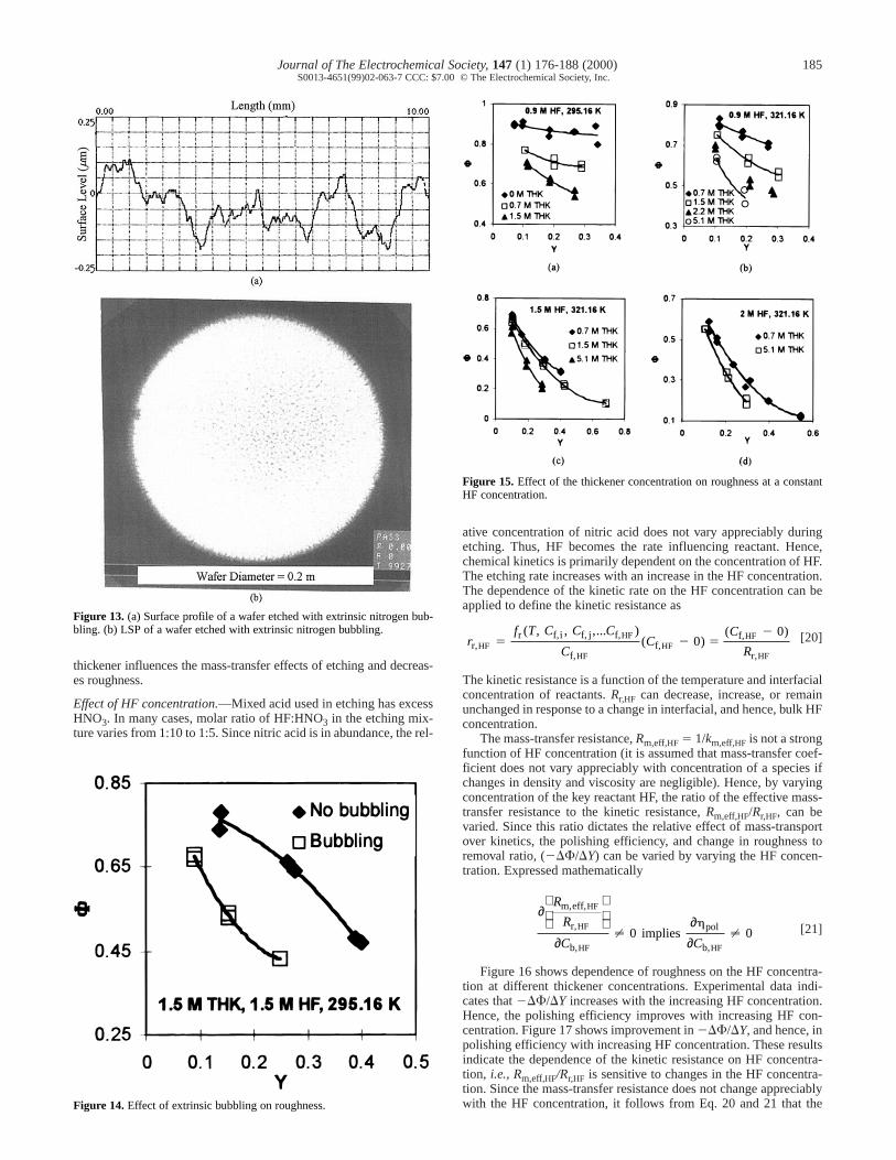
Figure 14 shows the effect of extrinsic bubbling on the surfaceroughness. Rough silicon wafers with very low gloss (0-5 glossunits) and high f (0.2-0.3 mm) were etched with and without extrin-sic nitrogen bubbling in a 1.5 M HF 1 1.5 M H3PO4 1 excessHNO3 mixture. Improvement in the roughness was very poor whenthe intrinsic bubble masking effect was present,i.e., when Rm,g washigher. Rm,g is lower when the extrinsic bubbling is present,andhence, polishing efficiency and reduction in roughness were higherin the presence of the extrinsic bubbling. Thus,roughness of etchedsilicon wafers etched under different hydrodynamic conditions canbe explained by the proposed phenomenological model.
Effect of overall mass-transfer.—A series of experiments wasperformed using the setup described in Fig. 7a to establish the effectof mass-transport on improvement in roughness of etched wafers.The experiments were conducted with and without the viscous thick-ener (H3PO4) at various HF concentrations and at different tempera-
Figure 10. (a) Surface profile of a wafer etched at 5 rpm with no extrinsicbubbling. (b) LSP of a wafer etched at 5 rpm with no extrinsic bubbling.

184 Journal of The Electrochemical Society, 147 (1) 176-188 (2000)S0013-4651(99)02-063-7 CCC:$7.00 © The Electrochemical Society, Inc.
tures with wafers rotating at 6 rpm and at approximately 6 3 105 Paupstream nitrogen pressure. Rough silicon wafers with very lowgloss (0-5 gloss units) and high f (0.2-0.3 mm) were etched in allexperiments discussed below.
Effect of thickener.—A mixture of HF and HNO3 has density andviscosity closer to those of water. Hence, the mass-transfer resis-tance or the thickness of the effective transport-film for such a mix-ture can be quite low. Addition of a thick viscous acid to this mix-ture, which does not chemically participate in the etching reactionshould not alter the chemical kinetics,but should increase the mass-transfer resistance as a result of the increase in the viscosity, i.e.,∂(km,eff,HF)/∂m < 0 implies ∂(Rm,eff,HF)/∂m > 0 implies∂(Rm,eff,HF)/∂Cb,thk > 0. Since the bulk viscosity increases with con-centration of the thickener, the effective mass-transfer resistanceincreases with the concentration of the thickener.
In the industry, it has been observed that addition of a few viscousacids to the mixture of HF and HNO3 decreases the roughness of thewafer more efficiently for the same removal. As discussed earlier,addition of a thickener increases the effective mass-transfer resistance(Rm,eff,HF). Thus,Rm,eff,HF/Rr,HF increases with the thickener concen-tration, i.e., ∂(Rm,eff,HF/Rr,HF)/∂Cb,thk > 0. It follows from Eq. 14 and 19that the ratio of change in roughness to removal improves withincreasing difference between the removal rates at peaks and valleys.This difference increases with increasing mass-transfer effects ifthickness of the mass-transfer film is below the optimum (Fig. 4 and6c). Thus,increasing concentration of the thickener must increase thepolishing efficiency, i.e., roughness to removal ratio (2DF/DY), must
Figure 11. (a) Surface profile of a wafer etched at 60 rpm with no extrinsicbubbling. (b) LSP of a wafer etched at 60 rpm with no extrinsic bubbling.
also improve. Figure 15 shows the effect of the thickener concentra-tion on the roughness to removal ratio. It is clearly observed that the
Figure 12. (a) LSP of a wafer etched at 60 rpm and at a lower HF concen-tration. (b). Central surface profile of a wafer etched at 60 rpm and at a lowerHF concentration. (c). Peripheral surface profile of a wafer etched at 60 rpmand a lower HF concentration.
Journal of The Electrochemical Society, 147 (1) 176-188 (2000) 185S0013-4651(99)02-063-7CCC:$7.00 © The Electrochemical Society, Inc.
thickener influences the mass-transfer effects of etching and decreas-es roughness.
Effect of HF concentration.—Mixed acid used in etching has excessHNO3. In many cases,molar ratio of HF:HNO3 in the etching mix-ture varies from 1:10 to 1:5. Since nitric acid is in abundance, the rel-
Figure 13. (a) Surface profile of a wafer etched with extrinsic nitrogen bub-bling. (b) LSP of a wafer etched with extrinsic nitrogen bubbling.
Figure 14. Effect of extrinsic bubbling on roughness.
ative concentration of nitric acid does not vary appreciably duringetching. Thus, HF becomes the rate influencing reactant. Hence,chemical kinetics is primarily dependent on the concentration of HF.The etching rate increases with an increase in the HF concentration.The dependence of the kinetic rate on the HF concentration can beapplied to define the kinetic resistance as
[20]
The kinetic resistance is a function of the temperature and interfacialconcentration of reactants. Rr,HF can decrease, increase, or remainunchanged in response to a change in interfacial,and hence, bulk HFconcentration.
The mass-transfer resistance, Rm,eff,HF 5 1/km,eff,HF is not a strongfunction of HF concentration (it is assumed that mass-transfer coef-ficient does not vary appreciably with concentration of a species ifchanges in density and viscosity are negligible). Hence, by varyingconcentration of the key reactant HF, the ratio of the effective mass-transfer resistance to the kinetic resistance, Rm,eff,HF/Rr,HF, can bevaried. Since this ratio dictates the relative effect of mass-transportover kinetics,the polishing efficiency, and change in roughness toremoval ratio, (2DF/DY) can be varied by varying the HF concen-tration. Expressed mathematically
[21]
Figure 16 shows dependence of roughness on the HF concentra-tion at different thickener concentrations. Experimental data indi-cates that 2DF/DY increases with the increasing HF concentration.Hence, the polishing efficiency improves with increasing HF con-centration. Figure 17 shows improvement in 2DF/DY, and hence, inpolishing efficiency with increasing HF concentration. These resultsindicate the dependence of the kinetic resistance on HF concentra-tion, i.e., Rm,eff,HF/Rr,HF is sensitive to changes in the HF concentra-tion. Since the mass-transfer resistance does not change appreciablywith the HF concentration, it follows from Eq.20 and 21 that the
∂
∂∂
∂
R
R
C C
m,eff,
r,
b,
pol
b,
HF
HF
HF HF
implies
? ?0 0
h
rf T C C C
CC
C
Rr,r f,i f, j f,
f,f,
f,
r,HF
HF
HFHF
HF
HF
5 2 52( , , ,... )
( )( )
00
Figure 15. Effect of the thickener concentration on roughness at a constantHF concentration.

186 Journal of The Electrochemical Society, 147 (1) 176-188 (2000)S0013-4651(99)02-063-7 CCC:$7.00 © The Electrochemical Society, Inc.
y
kinetic resistance changes with HF concentration. It also implies thatthe kinetic rate is a stronger function of HF concentration than themass-transfer rate is. Thus,the HF concentration can be increased toimprove polishing efficiency. However, at higher HF concentrationsetching rates are uncontrollably high, and process control and run-away become a concern. The etching reaction is exothermic innature, and hence, at high removal rates,the heat generation rate caneasily exceed the heat removal rate by plastic heat exchangers whichmust be used in the corrosive etching environment.
Effect of temperature.—The etchant temperature, like the concentra-tion of HF species,can affect the kinetic resistance. It can also affectthe mass-transfer resistance. Typically the kinetic rate increases withan increase in temperature because of the exponential dependence ofthe kinetic rate constant on the temperature. The mass-transfer rate
Figure 16. Effect of HF concentration on roughness at a constant thickenerconcentration.
Figure 17. Effect of HF concentration on roughness.
also increases with temperature because both viscosity and densitof liquids decrease with increasing temperature. Thus
[22]
Thus both Rr,HF and Rm,eff,HF decrease with increasing temperature.For reactions which have weak dependence on the temperature, kinet-ic effects increase with temperature, i.e., ∂(Rm,eff,HF/Rr,HF)/∂T < 0 andfor reactions which have strong dependence on the temperature,mass-transfer effects increase with increasing temperature, i.e.,∂(Rm,eff,HF/Rr,HF)/∂T > 0. As shown in Fig. 18,when changes in boththe kinetic and mass-transfer resistances are comparable, there is noincremental effect of temperature on the polishing efficiency, i.e.,∂(Rm,eff,HF/Rr,HF)/∂T < 0. However, dependence of these parameterson the temperature can be different under different etching conditions.A few experiments conducted to study effects of temperature yieldedunclear results.
Conclusions
Silicon etching is a mass-transfer influenced three-phase system.The three-phase etching system can be phenomenologically mod-eled as a two-phase system. Mass-transfer and kinetic influences onetching process are explained by the ratio of the effective mass-transfer resistance to the kinetic resistance.
A rough silicon wafer is a field of peaks and valleys characterizedby an average roughness,f. In a mass-transfer influenced system,etching rates at peaks are higher than the etching rates at valleys asa result of the difference in the local mass-transfer resistances. Thus,in the presence of the mass-transfer resistance chemical polishingtakes place. Dependence of polishing efficiency (the ratio of actualpolishing rate to the maximum possible polishing rate) on the ratioof effective mass-transfer resistance to kinetic resistance is explainedusing the proposed phenomenological model and experimental data.
Gaseous products of the etching reaction form the intrinsic bub-bles that mask local sites on the silicon wafer surface, which leads tosurface irregularities that are explained by the bubble-masking ef-fect. The effects of the bubble detachment from the surface, and bub-ble and HF transport through the mass-transfer film are lumped in aneffective mass-transfer resistance. In the absence of excessive bub-ble-masking effect, the polishing efficiency increases with the ratioof the effective mass-transfer resistance to the kinetic resistance,reaches an optimum and then decreases. When this ratio is greaterthan the critical bubble masking resistance value, the bubble-mask-
∂∂
∂∂
∂∂
R
T
k
T
R
Tr, m, m,eff,HF HF HFand implies< > <0 0 0
Figure 18. Effect of temperature on roughness.
Journal of The Electrochemical Society, 147 (1) 176-188 (2000) 187S0013-4651(99)02-063-7CCC:$7.00 © The Electrochemical Society, Inc.
ing is significant,and hence, the polishing efficiency decreases. Re-duction in the polishing efficiency can also result by a reduction inthe difference between the etching rates at peaks and valleys for veryhigh mass-transfer resistances.
Addition of a thickener increases the mass-transfer resistance.Thus,the ratio of the mass-transfer resistance to kinetic resistancecan be increased by addition of an inert thickener. Also, the kineticresistance changes with changing HF concentration with negligibleeffect on the mass-transfer resistance. Hence, this ratio can also becontrolled by varying the HF concentration. When both the mass-transfer resistance and kinetic resistance show comparable changewith temperature, polishing efficiency does not change appreciablywith temperature.
Thus,the ratio of the effective mass-transfer resistance to kineticresistance must be higher than the critical minimum value and lowerthan the critical bubble masking value to achieve a high polishingefficiency.
Acknowledgments
The authors acknowledge the Operations Technology Departmentof MEMC at Kuala Lumpur for implementing the new etching processbased on this research. The authors also thank Judy Schmidt, ShawnPatton,and Tom Doane for their help in conducting experiments.
MEMC Electronic Materials, Incorporated, assisted in meeting the publi -cation costs of this article.
AppendixIn semiconductor industries “gloss” is used with “roughness”as
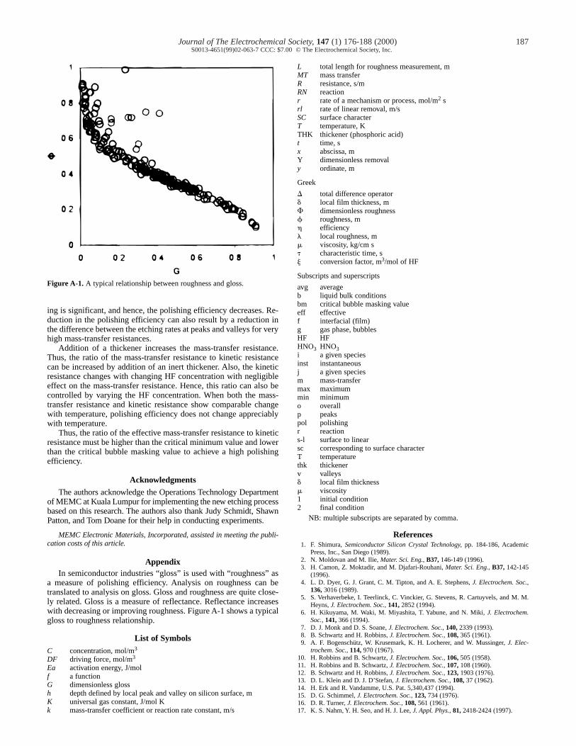
a measure of polishing efficiency. Analysis on roughness can betranslated to analysis on gloss. Gloss and roughness are quite close-ly related. Gloss is a measure of reflectance. Reflectance increaseswith decreasing or improving roughness. Figure A-1 shows a typicalgloss to roughness relationship.
List of Symbols
C concentration, mol/m3
DF driving force, mol/m3
Ea activation energy, J/molf a functionG dimensionless glossh depth defined by local peak and valley on silicon surface, mK universal gas constant,J/mol Kk mass-transfer coefficient or reaction rate constant,m/s
Figure A-1. A typical relationship between roughness and gloss.
L total length for roughness measurement,mMT mass transferR resistance, s/mRN reactionr rate of a mechanism or process,mol/m2 srl rate of linear removal, m/sSC surface characterT temperature, KTHK thickener (phosphoric acid)t time, sx abscissa,mY dimensionless removaly ordinate, m
Greek
D total difference operatord local film thickness,mF dimensionless roughnessf roughness,mh efficiencyl local roughness,mm viscosity, kg/cm st characteristic time, sj conversion factor, m3/mol of HF
Subscripts and superscripts
avg averageb liquid bulk conditionsbm critical bubble masking valueeff effectivef interfacial (film)g gas phase, bubblesHF HFHNO3 HNO3i a given speciesinst instantaneousj a given speciesm mass-transfermax maximummin minimumo overallp peakspol polishingr reactions-l surface to linearsc corresponding to surface characterT temperaturethk thickenerv valleysd local film thicknessm viscosity1 initial condition2 final condition
NB: multiple subscripts are separated by comma.
References1. F. Shimura, Semiconductor Silicon Crystal Technology, pp. 184-186,Academic
Press,Inc., San Diego (1989).2. N. Moldovan and M. Ilie, Mater. Sci. Eng., B37,146-149 (1996).3. H. Camon,Z. Moktadir, and M. Djafari-Rouhani,Mater. Sci. Eng., B37, 142-145
(1996).4. L. D. Dyer, G. J. Grant, C. M. Tipton, and A. E. Stephens,J. Electrochem. Soc.,
136,3016 (1989).5. S. Verhaverbeke, I. Teerlinck, C. Vinckier, G. Stevens,R. Cartuyvels, and M. M.
Heyns,J. Electrochem. Soc., 141,2852 (1994).6. H. Kikuyama,M. Waki, M. Miyashita,T. Yabune, and N. Miki, J. Electrochem.
Soc., 141,366 (1994).7. D. J. Monk and D. S. Soane, J. Electrochem. Soc., 140,2339 (1993).8. B. Schwartz and H. Robbins,J. Electrochem. Soc., 108,365 (1961).9. A. F. Bogenschütz, W. Krusemark, K. H. Locherer, and W. Mussinger, J. Elec-
trochem. Soc., 114,970 (1967).10. H. Robbins and B. Schwartz, J. Electrochem. Soc., 106,505 (1958).11. H. Robbins and B. Schwartz, J. Electrochem. Soc., 107,108 (1960).12. B. Schwartz and H. Robbins,J. Electrochem. Soc., 123,1903 (1976).13. D. L. Klein and D. J. D’Stefan,J. Electrochem. Soc., 108,37 (1962).14. H. Erk and R. Vandamme, U.S. Pat. 5,340,437 (1994).15. D. G. Schimmel,J. Electrochem. Soc., 123,734 (1976).16. D. R. Turner, J. Electrochem. Soc., 108,561 (1961).17. K. S. Nahm,Y. H. Seo,and H. J. Lee, J. Appl. Phys.,81,2418-2424 (1997).

188 Journal of The Electrochemical Society, 147 (1) 176-188 (2000)S0013-4651(99)02-063-7 CCC:$7.00 © The Electrochemical Society, Inc.
18. D. G. Schimmel and M. J. Elkind, J. Electrochem. Soc., 125,152 (1978). 19. R. W. Fathauer, T. George, A. Ksendzov, and R. P. Vasquez,Appl. Phys. Lett.,60,
995 (1992). 20. K. Gaffney and H. D. Chiou,Abstract 502,The Electrochemical Society Meeting
Abstracts,Vol. 98-1,San Diego, CA, May 3-8,1998.21. Th. Bauer, L. Farbry, T. Teuschler, G. Schwab, and M. Stadler, Abstract 321,The
Electrochemical Society Meeting Abstracts,Vol. 98-1,San Diego, CA, May 3-8,1998.
22. I. E. Berishev, F. De Anda,V. A. Mishournyi, J. Olvera,N. D. Ilyinskaya,and V. I.Vasilyev, J. Electrochem. Soc., 142,L189 (1995).
23. K. McAndrews and P. Sukanek,J. Electrochem. Soc., 138,863 (1991).24. J. P. John and J. McDonald, J. Electrochem. Soc., 140,2622 (1993).
25. K. Osseo-Asare, D.Wei, and K. K. Mishra,J. Electrochem. Soc., 143,749 (1996).26. D. J. Monk,D. S. Soane, and R. T. Howe, J. Electrochem. Soc., 141,264 (1994).27. D. J. Monk,D. S. Soane, and R. T. Howe, J. Electrochem. Soc., 141,270 (1994).28. D. J. Monk,D. S. Soane, and R. T. Howe, Thin Solid Films,232,1 (1993).29. Y. Kunii, S. Nakayama,and M. Maeda,J. Electrochem. Soc., 142,3510 (1995).30. T. Aoyama,T. Yamazaki,and T. Ito, J. Electrochem. Soc., 143,2280 (1996).31. O. Levenspiel,Chemical Reaction Engineering, 2nd ed., p. 349,Wiley Eastern
Limited, New Delhi (1972).32. R. H. Perry and D. W. Green,Chemical Engineer’s Handbook,6th ed., pp. 4.1-
4.91,McGraw-Hill, Inc., New York (1984).33. E. L. Cussler, Diffusion-Mass Transfer in Fluid Systems,pp. 75-78,Cambridge
University Press,Cambridge (1984).