A Real-Time Control System for a Frequency Response-based Permittivity Sensor.pdf
152
A REAL-TIME CONTROL SYSTEM FOR A FREQUENCY RESPONSE-BASED PERMITTIVITY SENSOR by NING TANG B.S., China Agricultural University, China, 2004 M.S., China Agricultural University, China, 2006 A THESIS submitted in partial fulfillment of the requirements for the degree MASTER OF SCIENCE Department of Biological and Agricultural Engineering College of Engineering KANSAS STATE UNIVERSITY Manhattan, Kansas 2009 Approved by: Major Professor Naiqian Zhang
-
Upload
kavita4123 -
Category
Documents
-
view
32 -
download
13
description
control system, pemittivity sensor
Transcript of A Real-Time Control System for a Frequency Response-based Permittivity Sensor.pdf

A REAL-TIME CONTROL SYSTEM FOR A FREQUENCY RESPONSE-BASED
PERMITTIVITY SENSOR
by
NING TANG
B.S., China Agricultural University, China, 2004 M.S., China Agricultural University, China, 2006
A THESIS
submitted in partial fulfillment of the requirements for the degree
MASTER OF SCIENCE
Department of Biological and Agricultural Engineering College of Engineering
KANSAS STATE UNIVERSITY Manhattan, Kansas
2009
Approved by:
Major Professor Naiqian Zhang

Abstract
Permittivity is an important property of dielectric materials. By measuring the
permittivity of a material, it is possible to obtain information about the material’s physical and
chemical properties, which are of great importance to many applications. In this study, a real-
time control system for a frequency-response (FR) permittivity sensor was developed. The core
of the hardware was a kitCON167 microcontroller (PHYTEC America, LLC), which controlled
and communicated with peripheral devices. The system consisted of circuits for waveform
generation, signal conditioning, signal processing, data acquisition, data display, data storage,
and temperature measurement. A C program was developed in the TASKING Embedded
Development Environment (EDE) to control the system.
The control system designed in this study embodied improvements over a previously
designed version in the following aspects: 1) it used a printed circuit board (PCB); 2) the
measurement frequency range was extended from 120 MHz to 400 MHz; 3) the resolution of
measured FR data was improved by using programmable gain amplifiers; 4) a data storage
module and a real-time temperature measurement module were added to the system; 5) an LCD
display and a keypad were added to the system to display the FR data with corresponding
frequencies and to allow users to enter commands.
Impedance transformation models for the sensor probe, the coaxial cable that connects
the control system with the sensor probe, and the signal processing circuit were studied in order

to acquire information on the permittivity of measured materials from measured FR data. Coaxial
cables of the same length terminated with different loads, including an open circuit, a short
circuit, a 50Ω resistor, and a 50Ω resistor paralleled by a capacitor, were tested. The results
indicated that the models were capable of predicting the impedances of these specific loads using
the FR data. Sensor probes with different sizes and coaxial cables with two different lengths
terminated with the same sensor probe were also tested. The results were discussed.
Additional tests for the gain and phase detector were conducted to compare FR data
measured by the gain and phase detector with those observed on an oscilloscope. The results
were discussed.

iv
Table of Contents
List of Figures ............................................................................................................................... vii
List of Tables ................................................................................................................................. xi
Acknowledgements....................................................................................................................... xii
CHAPTER 1 - Introduction ............................................................................................................ 1
CHAPTER 2 - Objectives............................................................................................................... 4
CHAPTER 3 - Literature Review................................................................................................... 5
3.1 Theory of permittivity........................................................................................................... 5
3.2 Permittivity measurement techniques................................................................................... 7
3.2.1 TDR................................................................................................................................ 7
3.2.2 Capacitance probe.......................................................................................................... 8
3.2.3 Resonator ..................................................................................................................... 10
3.2.4 Open-ended coaxial probe ........................................................................................... 12
3.2.5 Transmission line ......................................................................................................... 12
3.2.6 Free-space method ....................................................................................................... 13
CHAPTER 4 - Design of a Real-time Control System for the Permittivity Sensor ..................... 14
4.1 System Hardware Design.................................................................................................... 16
4.1.1 Microcontroller ............................................................................................................ 18
4.1.2 Signal generator ........................................................................................................... 21
4.1.2.1 Low frequency signal generator............................................................................ 21
4.1.2.2 High frequency signal generator........................................................................... 23
4.1.3 Multiplexer................................................................................................................... 25
4.1.4 Gain and phase detector ............................................................................................... 27
4.1.5 Programmable gain amplifier ...................................................................................... 30
4.1.6 LCD and keypad .......................................................................................................... 32
4.1.7 Temperature measurement........................................................................................... 34
4.1.8 Buffer amplifier ........................................................................................................... 36
4.1.9 Serial EEPROM........................................................................................................... 37
4.2 System Software Design..................................................................................................... 38

v
4.2.1 Low frequency signal generator................................................................................... 38
4.2.2 High frequency signal generator .................................................................................. 42
4.2.3 A/D module.................................................................................................................. 45
4.2.4 Programmable gain amplifier ...................................................................................... 46
4.2.5 Serial EEPROM........................................................................................................... 48
4.2.6 Microcontroller ............................................................................................................ 49
CHAPTER 5 - Impedance Transformation Models...................................................................... 52
5.1 Transmission line theory..................................................................................................... 52
5.1.1 Introduction of transmission line theory ...................................................................... 52
5.1.2 Coaxial cable................................................................................................................ 53
5.2 Sensor probe model ............................................................................................................ 58
5.3 Circuit model ...................................................................................................................... 61
5.3.1 Circuit model for the new control box ......................................................................... 61
5.3.2 Circuit model for the old control box........................................................................... 65
CHAPTER 6 - Experiment ........................................................................................................... 67
6.1 Sensor probes with different sizes ...................................................................................... 67
6.2 Coaxial cable of the same length with different loads........................................................ 68
6.2.1 Standard loads.............................................................................................................. 68
6.2.2 Parallel capacitor-resistor load..................................................................................... 69
6.3 Coaxial cables of different lengths with the same load ...................................................... 70
CHAPTER 7 - Results and Discussions ....................................................................................... 72
7.1 Sensor probes with different sizes ...................................................................................... 72
7.2 Coaxial cable of the same length with different loads........................................................ 77
7.2.1 Standard loads.............................................................................................................. 77
7.2.2 Parallel capacitor-resistor load..................................................................................... 87
7.3 Coaxial cables of different lengths with the same load ...................................................... 89
7.4 Problem with the gain and phase detector .......................................................................... 98
7.4.1 Test on a gain and phase detector evaluation board..................................................... 98
7.4.2 Test on the old control box at single frequencies....................................................... 102
7.4.3 Tests in single-frequency and frequency-sweep modes.............................................103

vi
7.4.3.1 Comparison of measurements by the control box and oscilloscope at the single
frequency mode............................................................................................................... 104
7.4.3.2 Comparison between single-frequency and frequency-sweep modes ................ 107
CHAPTER 8 - Conclusions ........................................................................................................ 111
8.1 Control system .................................................................................................................. 111
8.2 Impedance transformation models tests............................................................................ 111
CHAPTER 9 - Recommended Future Research......................................................................... 113
References................................................................................................................................... 115
Appendix A - Circuit schematic of the Control System ............................................................. 123
Appendix B - Circuit layout of the Control System ................................................................... 124
Appendix C - Microcontroller Program...................................................................................... 125
vii
List of Figures
Figure 4.1 Block diagram of the old control box.......................................................................... 15
Figure 4.2 Old control box (Zhang et al., 2006) ........................................................................... 15
Figure 4.3 The new control box.................................................................................................... 17
Figure 4.4 Functional diagram of the control system................................................................... 17
Figure 4.5 Connections between the I/O ports of microcontroller and peripheral devices .......... 18
Figure 4.6 Output Drivers in Push/Pull and Open Drain Modes .................................................. 21
Figure 4.7 Connection diagram of AD9833 ................................................................................. 22
Figure 4.8 Connections between kitCON-167 and AD9833 ........................................................ 22
Figure 4.9 Pin Diagram of AD8186.............................................................................................. 25
Figure 4.10 Schematic for the AD8186 multiplexer circuit ......................................................... 26
Figure 4.11 Two input signals for the gain and phase detector .................................................... 27
Figure 4.12 Idealized transfer characteristics for the gain and phase measurement mode (Analog
Devices, Inc., 2002) .............................................................................................................. 29
Figure 4.13 Basic connections in measurement mode with 30mV/dB and 10mV/degree scaling
(Analog Devices, Inc., 2002) ................................................................................................ 30
Figure 4.14 Pin connection diagram of MCP6S21 (Microchip Technology Inc., 2003).............. 31
Figure 4.15 Interface connections between kitCON-167 and MCP6S21..................................... 31
Figure 4.16 LCD and keypad........................................................................................................ 32
Figure 4.17 Pin connection diagram of AD623 (Analog Devices, Inc.)....................................... 35
Figure 4.18 Pin connection diagram of TS925 (STMicroelectronics, 1999)................................37
Figure 4.19 Connections between kitCON-167 and 25AA1024 .................................................. 38
Figure 4.20 Flow chart for the AD9833 signal generator............................................................. 42
Figure 4.21 Flow chart for the AD9858 signal generator............................................................. 45
Figure 4.22 Read sequence of 25AA1024 (Microchip Technology Inc., 2006)........................... 49
Figure 4.23 Byte write sequence of 25AA1024 (Microchip Technology Inc., 2006) .................. 49
Figure 4.24 Flow chart of the microcontroller program ............................................................... 50
Figure 5.1 Distributed impedance model for a transmission line (Coleman, 2004) ..................... 53
viii
Figure 5.2 Transmission line of length l terminated with a load .................................................. 56
Figure 5.3 Models for attenuation per unit length for the coaxial cable C1166 RG 58/U............ 58
Figure 5.4 Sensor probes............................................................................................................... 59
Figure 5.5 Circuit schematic for FR measurement using the new control box.............................61
Figure 5.6 Circuit schematic for FR measurement using the old control box .............................. 65
Figure 6.1 Coaxial cable with open, short and 50Ω loads ............................................................ 69
Figure 6.2 Coaxial cables.............................................................................................................. 71
Figure 7.1 Comparison of gains measured by the 7.5cm and 5cm probes ...................................73
Figure 7.2 Comparison of phases measured by the 7.5cm and 5cm probes ................................. 73
Figure 7.3 Comparison between the predicted and measured gain for the 5cm probe................. 74
Figure 7.4 Comparison between the predicted and measured phase for the 5cm probe............... 75
Figure 7.5 Comparison between the predicted and measured gain for the 7.5cm probe.............. 76
Figure 7.6 Comparison between the predicted and measured phase for the 7.5cm probe............ 76
Figure 7.7 Gain responses measured by the old control box for open, short and 50Ω loads on (a)
linear and (b) log scales ........................................................................................................ 77
Figure 7.8 Phase responses measured by the old control box for open, short and 50Ω loads on (a)
linear and (b) log scales ........................................................................................................ 78
Figure 7.9 Real and imaginary parts of ZL for the open circuit load measured by the old control
box......................................................................................................................................... 79
Figure 7.10 Real and imaginary parts of ZL for the short circuit load measured by the old control
box......................................................................................................................................... 80
Figure 7.11 Real and imaginary parts of ZL for the 50Ω resistor load measured by the old control
box......................................................................................................................................... 81
Figure 7.12 Gain responses measured by the new control box for open, short and 50Ω loads on
(a) linear and (b) log scales................................................................................................... 82
Figure 7.13 Phase responses measured by the new control box for open, short and 50Ω loads on
(a) linear and (b) log scales................................................................................................... 83
Figure 7.14 Real and imaginary parts of ZL for the 50Ω resistor load measured by the new
control box ............................................................................................................................ 84
Figure 7.15 Real and imaginary parts of ZL for the open load measured by the new control box 85
Figure 7.16 Real and imaginary parts of ZL for the short load measured by the new control box 86

ix
Figure 7.17 Comparison of real part of the load impedance measured by the old control box with
that calculated for the actual loads........................................................................................ 88
Figure 7.18 Comparison of imaginary part of the load impedance measured by the old control
box with that calculated for the actual loads......................................................................... 88
Figure 7.19 Gain responses measured using the short (37cm) and long (141cm) cables, both
terminated with a 50Ω resistor, on (a) linear and (b) log scales ........................................... 90
Figure 7.20 Phase responses measured using the short (37cm) and long (141cm) cables, both
terminated with a 50Ω resistor, on (a) linear and (b) log scales ........................................... 91
Figure 7.21 The real part of measured 50Ω load using the short (37cm) and long (141cm) cables
on (a) linear and (b) log scales .............................................................................................. 92
Figure 7.22 The imaginary part of measured 50Ω load using the short (37cm) and long (141cm)
cables on (a) linear and (b) log scales ................................................................................... 93
Figure 7.23 Gain responses measured using the short (37cm) and long (141cm) cables, both
terminated with the 7.5cm sensor probe, on (a) linear and (b) log scales............................. 94
Figure 7.24 Phase responses measured using the short (37cm) and long (141cm) cables, both
terminated with the 7.5cm sensor probe, on (a) linear and (b) log scales............................. 95
Figure 7.25 The real part of load impedance of the 7.5cm sensor probe measured using the short
(37cm) and long (141cm) cables, on (a) linear and (b) log scales ........................................ 96
Figure 7.26 The imaginary part of load impedance of the 7.5cm sensor probe measured using the
short (37cm) and long (141cm) cables, on (a) linear and (b) log scales ............................... 97
Figure 7.27 An RC circuit generated phase delays....................................................................... 98
Figure 7.28 Lissajous graph between two signals (Agilent 54621A, User’s Guide, 2000).......... 99
Figure 7.29 Phase delay observed from the oscilloscope and measured by the gain and phase
detector on a logarithmic frequency axis ............................................................................ 100
Figure 7.30 Phase delay observed from the oscilloscope and measured by the gain and phase
detector on a linear frequency axis ..................................................................................... 101
Figure 7.31 Signals on the INPA and INPB inputs of the gain and phase detector recorded by an
oscilloscope at (a) 50MHz, (b) 60 MHz, (c) 70 MHz, and (d) 80 MHz ............................. 103
Figure 7.32 Comparison of gain measured by the old control box with that observed on the
oscilloscope. The short cable was used in the test.............................................................. 105

x
Figure 7.33 Comparison of gain measured by the old control box with that observed on the
oscilloscope. The long cable was used in the test. .............................................................. 105
Figure 7.34 Comparison of phase measured by the old control box with that observed on the
oscilloscope. The short cable was used in the test.............................................................. 106
Figure 7.35 Comparison of phase measured by the old control box with that observed on the
oscilloscope. The long cable was used in the test. .............................................................. 106
Figure 7.36 Comparison of gain measured at the single frequency and the frequency sweep
modes. The short cable was used in the test. ...................................................................... 108
Figure 7.37 Comparison of gain measured at the single frequency and the frequency sweep
modes. The long cable was used in the test. ....................................................................... 108
Figure 7.38 Comparison of phase measured at the single frequency and the frequency sweep
modes. The short cable was used in the test. ...................................................................... 109
Figure 7.39 Comparison of phase measured at the single frequency and the frequency sweep
modes. The long cable was used in the test. ....................................................................... 109
Figure A.1 Circuit schematic of the control board in the new control box ................................ 123
Figure B.1 Circuit layout of the control board in the new control box....................................... 124

xi
List of Tables
Table 4.1 Boot-switch S3 (switch 1)............................................................................................. 19
Table 4.2 Chip-select signals S3 (switch 2 and 3) ........................................................................ 20
Table 4.3 I/O port configuration of kitCON167 for AD9858....................................................... 24
Table 4.4 I/O function of kitCON-167 for the LCDKBD1 .......................................................... 33
Table 4.5 LCDKBD1 address bus latch........................................................................................ 33
Table 4.6 Maximum attainable gain and resulting output swing for different input conditions
(Analog Devices, Inc., 1999) ................................................................................................ 36
Table 4.7 Function of Control Bits of the control register in AD9833......................................... 39
Table 4.8 Frequency Register Bits in AD9833 (Analog Devices, Inc., 2003b) ........................... 40
Table 4.9 SSCCON register for the synchronous serial interface of C167CR ............................. 41
Table 4.10 Register map for AD9858 (Analog Devices, Inc. 2003) ............................................ 44
Table 4.11 ADC result register of C167CR (Infineon technologies, 2000) ................................. 46
Table 4.12 Instruction register of MCP6S21 (Microchip Technology Inc., 2003)....................... 46
Table 4.13 Gain register of MCP6S21 (Microchip Technology Inc., 2003) ................................ 47
Table 4.14 Gain selected bits of MCP6S21 (Microchip Technology Inc., 2003) ........................ 47
Table 4.15 Instruction set (Microchip Technology Inc., 2006) .................................................... 48
Table 5.1 Signal attenuation in coaxial cable C1166 RG 58/U .................................................... 58

xii
Acknowledgements
I would like to express my deep gratitude to my major professor, Dr. Naiqian Zhang, for
his guidance and encouragement continually during the period of my master program study. He
has been a mentor, a father and a friend in my mind. His rigorous scholarship, meticulous
research spirit influenced me deeply and will play an important role for my future life and career.
I am also grateful for the opportunities he supplied to me so that I have this chance to study in
the US.
I would like to extend my sincere gratitude to my supervisory committee members, Dr.
William B. Kuhn, Dr. Mitchell L. Neilsen. Thanks to Dr. Kuhn for his patience and kindness, for
spending his precious time on answering my questions on the transmission problems, for giving
me many suggestions and guidance. Thanks to Dr. Neilsen for his suggestions and help on part
of the software design.
I would like to thank many experts who helped me overcome the obstacles during my
master program. I thank Dr. Donald Lenhert for his suggestions on solving the hardware problem
of the microcontroller. I thank Dr. Philip L. Barnes for guiding me to know the concentration of
the harmful impurities in water. I thank Dr. Stoyan Ganchev at Agilent Technologies for helping
me setting up the impedance analyzer and giving me many suggestions on how to calibrate. I
thank many technical supports at Analog Devices, Inc. for answering me many questions on the

xiii
DDS evaluation board and guiding me how to modify it so that it can be well used for my
research.
My gratitude also goes to Mr. Darrell Oard for his valuable suggestions and assistance in
constructing the sensor probe and guiding me how to use the mechanical machines in the
workshop. Many thanks to Mrs. Barb Moore and Mr. Randy Erickson for helping me in all
related to my study and research in the department.
Profound thanks and appreciation also go to Dr. Gary A. Clark, the former department
head, Dr. Joe P. Harner, the current department head, Dr. James M. Steichen, Dr. Donghai
Wang, Dr. Wenqiao Yuan, and all other faculty members and staff in the department.
I also would like to extend my gratitude to all the fellow students in the Instrumentation
and Control Lab: Ms. Yali Zhang, Mr. Wei Han, Mr. Peng Li, Ms. Ling Xue, Dr. Jizhong Deng,
Ms. Sarah Shultz and Mr. Alan Bauerly for their help on my research and profound friendship
among us.
Finally, my deep appreciation is given to my family for their patience, continuous support
and encouragement, which have made me finish my study smoothly. Special thanks are given to
my husband, Peng Li, who is also a student in the Instrumentation and Control Lab, for his
academic suggestions and help on my research, for his support and encouragement when I met
difficulties, for his patience and unconditional love during the life, which have helped me
complete my master program study.

1
CHAPTER 1 - Introduction
Permittivity is a physical quantity that describes the dielectric and conductive properties
of dielectric materials. It is determined by the ability of a material to polarize in response to an
electric field, and thereby reduce the total electric field inside the material. When an external
electric field is applied to a dielectric material, dipole molecules in the material tend to align up
in the opposite directions. This process of alignment, called polarization, hinders current flow.
The response of a material to an external alternating electric field typically depends on the
frequency of the electric field. Therefore, permittivity of dielectric materials is frequency-
dependent.
Permittivity is an important characteristic of a material. By knowing the dielectric
property of a material, it is possible to obtain information about its physical and chemical
properties, which are of great importance to many applications in industry, agriculture,
production of food, and biological materials, and medicine. For example, dielectric property was
used to study the moisture content in grain and other materials, and to measure fruit maturity
(Nelson 1991; Nelson et al., 1995). During microwave heating, reflection, transmission, and
absorption of microwave energy are controlled by the dielectric properties of the materials.
Therefore, dielectric property plays an important role in studying the absorption of
electromagnetic energy (Tanaka et al., 2002). Moreover, dielectric properties of materials are
important in the design of electrical and electronic equipment where they are used as insulating
components, in studying biological substances, as well as thin plates of semiconductor and
magnetic materials (Nelson 2003; Stuchly et al., 1974). Because of the wide application areas of
2
dielectric properties, there is an increasing demand for various dielectric materials. As a result,
more and more researchers have proposed many different methods for measuring the permittivity
of dielectric materials.
Since the permittivity of a dielectric material is a function of frequency, study of
permittivity should be conducted in a wide range of frequencies. However, the frequency range
of dielectric spectroscopy covers nearly 21 orders of magnitude from 10−6 to 1015 Hz; no single
method of permittivity measurement is able to cover this range. Therefore, different
measurement techniques are adopted for different applications, depending on the frequency of
interest, the nature of the dielectric material to be measured, and the degree of accuracy required.
Normally, at the low frequency range of 10−6~103 Hz, time domain measurement is frequently
used. Frequency domain measurement is adequate for the frequency range of 10−5~106 Hz.
Reflective coaxial methods and transmission coaxial methods are frequently used for the
frequency ranges of 106~1010 Hz and 108~1011 Hz, respectively. Fourier-transform methods are
working in the frequency range of 1011~1015 Hz (Chen et al., 2004).
Some measurement techniques can cover a relatively wide frequency range. For example,
conventional bridges are used over a frequency range of approximately 50Hz to 25MHz. A Q-
meter is suitable for a rather higher band of frequencies, from 100 kHz to 100 MHz. The
principle of the bridge and Q-meter is to measure the capacitance and conductance of a material,
because a material can be modeled electrically as a series or parallel equivalent circuit at any
given radio frequency. If the circuit parameter, such as impedance or admittance, can be
measured appropriately, the dielectric properties of the material can be determined at that

3
particular frequency (Nelson 1999).
Many researchers have been conducting research on the development of dielectric
property measurement instruments based on different measurement principles. Stoakes and
Brock (1973) designed a permittivity sensor using a capacitor method to determine the
permittivity of oil and its lubricating ability. This oil permittivity sensor obtained a United States
Patent. A dielectric sensor using the principle of resonant cavity was developed by Fort Motor
Co in early 1990s to measure alcohol concentration in methanol or ethanol-gasoline blends
(Meitzler and Saloka, 1992). Hewlett Packard (HP) developed impedance, spectrum or network
analyzers with high accuracy to measure permittivity. However, these analyzers are very
expensive and need complicated calibrations.
A permittivity sensor using a frequency-response (FR) method for simultaneous
measurement of multiple properties of dielectric materials in real time has been developed by
researchers in the Instrumentation and Control Laboratory of the Biological and Agricultural
Engineering Department at Kansas State University since 2000. The sensor was originally
developed to measure soil properties (Fan, 2002; Zhang et al., 2004; Lee, 2005; Lee et al., 2007a;
Lee and Zhang, 2007b). Since 2005, the sensor has been modified to measure other dielectric
materials – water, biofuel, and air (Zhang et al., 2006; Zhang et al., 2007). In 2005, a control box
was developed to control the modified sensor. In this study, a new control box was developed to
improve the performance of the sensor. This thesis describes the hardware and software of the
new control box. Studies on impedance transformation models for the sensor probe and the
control box are also reported in this thesis.

4
CHAPTER 2 - Objectives
The overall objective of this research is to develop a real-time control system with
improvements over a previously developed version for a FR permittivity sensor.
Specific objectives are as follows:
1. Develop an integrated, microcontroller-based system, including circuits for waveform
generation, signal conditioning, signal processing, data collection, data display, data
storage, and temperature measurement.
2. Develop a C program to control the system.
3. Investigate impedance transformation models for the sensor probe, the coaxial cable that
connects the control system with the sensor probe, and the signal processing circuit with
a goal of obtaining information on the permittivity of measured materials from measured
FR data.

5
CHAPTER 3 - Literature Review
3.1 Theory of permittivity
The term “permittivity” used in this thesis implies the relative complex permittivity,
which is the permittivity of a material relative to that of free space (Equation 3.1).
0rε ε ε= (3.1)
' ''r r rjε ε ε= − (3.2)
where ε is permittivity,
rε is relative permittivity,
0ε = 8.85 ×10⁻¹² F m-1 (permittivity of free space),
'rε is dielectric constant, and
''rε is dielectric loss factor.
The real part of the relative permittivity is dielectric constant, which describes energy
storage in the material. The imaginary part is loss factor, which describes the rate of energy
dissipation in the material (Nelson, 2003). Dielectric constant and dielectric loss factor can be
expressed by the following equations:

6
'' ''
0r d
σε ε ωε= + (3.3)
''
'
tanr
rεε δ= (3.4)
where ''dε is dielectric loss,
σ is electrical conductivity,
ω is angular frequency,
0
σωε is conductive loss, and
δ is loss angle.
Permittivity is a good indicator of multiple material properties and is frequency-
dependent. Both the real and imaginary parts of relative permittivity are dependent on frequency.
At low frequencies, the energy dissipation process 0
σωε caused by ionic conduction is
inversely proportional to frequency and becomes critical for energy loss. The polarity of the
electric field changes slowly enough at such frequencies to allow dipole molecules in the
material to reach equilibrium before the electric field has changed. For frequencies at which
dipole orientation can not follow the applied electric field due to the binding force between
atoms, absorption of the field’s energy leads to energy dissipation, in the form of dielectric
relaxation (Robinson et al., 2003; Topp et al., 2000). Therefore, dipolar energy dissipation is the
predominant loss at high frequencies. The combination of polarization, relaxation, and ionic
conduction makes the interpretation of dielectric properties of materials complex. Changes of

7
any of these three properties caused by changes in material composition can be detected by
complete measurement of permittivity (Lee, 2005).
3.2 Permittivity measurement techniques
Many papers reporting diverse methods for permittivity measurement can be found in the
literature. Many researchers all over the world also studied on different methods for permittivity
measurement. Many types of permittivity sensors and instruments have been developed as
modern electronics fast evolving. Choices of measurement methods for particular applications
depend upon the physical and electrical properties of the material under test, the frequency range
of interest, and the operative constraints. The most commonly used techniques - time domain
reflectometry (TDR), capacitance probe, transmission line, resonator, open-ended coaxial probe,
and free-space method, are reviewed in this section.
3.2.1 TDR
The TDR method was developed in the 1980s and has become a major technique for
permittivity measurement since then (Afsar et al., 1986). This method covers a wide frequency
range from radio frequency to microwave (Nozaki and Bose, 1990). The basic principle of TDR
measurement is to measure the time difference between the reflected and the incident pulse,
which was produced by a step voltage pulse generator, through a coaxial line. The recorded time
difference can be related to the dielectric properties of materials.
Topp and Davis (1985) used the TDR method to measure volumetric water content of
unsaturated soils. A strong relationship between the volumetric water content and dielectric
constant for a wide range of soils was reported. Sri Ranjan and Domytrak (1997) measured
8
effective volume of soils using different TDR miniprobes with three and five rods, respectively.
The result showed that the three-rod miniprobes were easier to install. However, orientation of
the three-rod miniprobes easily influenced the effective volume measured in saturated soils.
Robinson et al. (1999) adopted the TDR method in measuring relative permittivity of sandy soils.
Payero et al. (2006) used TDR to continuously monitor the nitrate-nitrogen in soil and water.
Good correlation, between the bulk electrical conductivity measurements by TDR in water and
nitrate-nitrogen concentrations, was achieved.
3.2.2 Capacitance probe
Robinson et al. (1999) adopted a surface capacitance insertion probe (SCIP) to measure
relative permittivity of sandy soils. The SCIP consists of two parallel stainless steel electrodes
which define a capacitor. The capacitance is a function of the relative permittivity of the material
where the probe is embedded and the geometric configuration of the probe:
0rC gε ε= (3.5)
where C is the capacitance,
rε is relative permittivity, and
g is a geometric constant.
The capacitor formed by the probe and an inductor form an oscillator circuit. The
frequency of oscillation is a function of both the inductance and capacitance in the circuit
(Equation 3.6) (Dean et al., 1987). Therefore, permittivity of the material embedding the probe
can be derived by measuring the oscillation frequency.

9
1
2F
LCπ= (3.6)
where L is the circuit inductance, and
C is the capacitance of the probe embedded in the material to be measured.
Lee (2005) developed a frequency-response permittivity sensor, with a four-electrode
probe arranged in a Wenner-array structure, for simultaneously measuring multiple soil
properties. The sensor probe consisted of four rectangular metal plates. In order to increase the
capacitance effect, a relatively large plate area and a relatively small separation between the
plates were chosen. Impedance of the probe inserted in the materials to be tested can be related to
the relative permittivity of the material to be tested:
'
0r
Cgε
ε= (3.7)
''
02r
Gg
fε
π ε= (3.8)
where C is the capacitance between the plates,
G is the conductance between the plates, and
g is the geometric factor of the sensor.
10
The geometric factor was determined from the conductivity σ of the medium surrounding
the sensor probe (material to be tested) and the load resistance R measured between sensor
electrodes.
1R g gρ
σ= = (3.9)
g Rσ= (3.10)
where ρ is the resistance of the material, and
σ is the conductivity of the material.
3.2.3 Resonator
Depending on the type of transmission line used, microwave resonators have different
names such as coaxial, microstrip, slotline, and cavity resonator (Nyfors, 2000). In general, a
microwave resonant cavity is a box fabricated from high-conductivity metal. The shape of the
cavity is always rectangular or cylindrical so that the distribution of electric and magnetic inside
is easily calculated. The size of the cavity is inversely proportional to the desired frequency. That
is, for higher frequencies, the cavity should be smaller.
The basic principle of the resonant method is that the resonant frequency shifts and the
energy absorption characteristics change when a resonator is filled with a sample. Changes in the
resonant frequency provide information that can be used to calculate the real part of material
permittivity - dielectric constant. Changes in the energy absorption, which can be expressed as
11
Q-factor (ratio of energy stored to energy dissipated), are used to estimate the imaginary part of
the material permittivity - dielectric loss (Venkatesh and Raghavan, 2005).
As early as 1960s, the resonant cavity technique was frequently used for studying the
dielectric properties of materials at microwave frequencies. This technique still has a unique
place now, owing to its high sensitivity and relative simplicity. Especially when data are required
at only one microwave frequency, the resonant cavity method is probably the most logical choice
(Bussey, 1967). Yu et al. (2000) proposed an approach using a cylindrical cavity resonator to
measure the complex permittivity of lossy liquids.
Matytsin et al. (1996) proposed a method of dielectric permittivity measurement based on
a slotted coaxial resonator with decimeter wavelengths, which can be applied in industry for non-
destructive testing of sheet materials. Raveendranath et al. (1996) used an open-ended coaxial
resonator to measure the complex permittivity of water within the frequency range from 0.6 GHz
to 14 GHz. Dudorov et al. (2005) developed a method using a spherical open resonator at
millimeter wavelengths for dielectric constant measurement of thin films on optically dense
substrates.
Many researchers developed sensors based on the resonant technique. Dionigi et al.
(2004) designed a resonant sensor for dielectric permittivity measurements of powdered,
granular and liquid materials. The results on measuring silica sand are of good accuracy.
Fratticcioli et al. (2004) developed a microstrip resonant sensor, its equivalent circuit, and the
driving electronic circuitry for the measurement of material permittivity.
12
3.2.4 Open-ended coaxial probe
The coaxial probe method is a modification base on the transmission line method. It
measures the reflected signal from a material through a coaxial line ending with a tip, which is in
contact with the material being tested. The tip is located at the center of a probe. For measuring
solid materials, the probe needs to touch a flat surface of the material. For liquid, on the other
hand, the probe needs to be immersed in the liquid during measurement. The measured reflection
coefficient is related to the sample permittivity (Sheen and Woodhead, 1999). The coaxial
probe method is easy to use because it does not require a particular sample shape or special
containers. Moreover, it is possible to measure the dielectric properties over a wide range of
frequencies, from 500 MHz to 110 GHz. However, this method requires elaborate calibration
procedures. It is also of limited accuracy with the materials with low relative permittivity values
(Venkatesh and Raghavan, 2005).
3.2.5 Transmission line
Transmission line techniques based on one-port measurements or two-port measurements
have been broadly used over the past 50 years (Catala-Civera et al., 2003). Transmission lines
have many different forms: coaxial cable, waveguide, and microstrip lines. The principle of the
transmission line technique is that when an incident signal in an electromagnetic field transmits
through a sample, which is precisely fully filled in an enclosed transmission line, the related
measured S-parameters for the reflection and transmission can provide the information on the
permittivity of the materials (Baker-Jarvis et al., 1990).
Abdulnour et al. (1995) proposed to use discontinuity in a rectangular waveguide to
measure the permittivity of dielectric materials. Bois et al. (1999) reported a permittivity

13
measurement technique that uses dielectric plug-loaded, two-port transmission line to measure
the dielectric property of granular and liquid materials, such as cement powder, corn oil,
antifreeze solution, and tap water. Ocera et al. (2006) reported a technique for measuring
complex permittivity based on a four-port device using microstrip.
The transmission line method is of good accuracy and sensitive, but it is difficult to use
and time consuming. It covers a narrower range of frequencies, compared to the coaxial probe
method. Moreover, the thickness of the sample for the transmission line method should be one-
quarter of the wavelength of the signal source that penetrated the sample. Therefore, at lower
frequencies, the sample size has to be quite large.
3.2.6 Free-space method
The free-space method is also based on transmission line techniques. It is a non-
destructive and contact-less measuring method. This method uses two antennas, one transmitting
and the other receiving. The principle is to measure the attenuation and phase shift of a
microwave signal, which transmits through the material under test along the path from the
transmitting antenna to the receiving antenna. The measured attenuation and phase shift can be
used to compute the permittivity of the material. Ghodgaonkar et al. (1990) used the free-space
method to measure the complex permittivity of various materials, such as teflon, sodium
borosilicate glass, and microwave-absorbing materials. Trabelsi and Nelson (2003) also used the
free-space transmission method to measure the dielectric properties of cereal grain and oilseed.

14
CHAPTER 4 - Design of a Real-time Control System for the
Permittivity Sensor
A real-time control system for the FR permittivity sensor was developed in this study.
This control system was developed based upon a previous version (Zhang et al., 2006). In this
thesis, the previously developed control system will be referred to as the “old control box”,
whereas the control system developed in this study will be referred to as the “new control box”
hereafter.
A functional block diagram of the old control box is shown in Figure 4.1. It consisted of a
microcontroller, a signal generator, and a gain and phase detector. The signal generator generated
sinusoidal waves with frequencies up to 120 MHz. The signal from the signal generator was sent
to channel A of the gain and phase detector. The signal from the output of a voltage divider that
consisted of a constant resistance Rref and impedance Zin was sent to channel B. Thus, the gain
and phase detector measured FR of the following transfer function:
ref inA
B in
R ZV
V Z
+= (4.1)
The output signals for gain (VMAG) and phase (VPHS) from the gain and phase detector
were sent to the microcontroller for processing. Because Zin can be related the sensor probe
impedance Zload through impedance transformation, Zload at given frequencies can be derived

15
from the measured gains and phases at these frequencies. The old control box is shown in Figure
4.2.
Figure 4.1 Block diagram of the old control box
kitCON-167Microcontroller
AD9854Signal Generator
Evaluation Board
AD8302Gain & Phase
Detector Evaluation Board
Sensor
Zin
Rref
A
B
VMAG
VPHS
kitCON-167Microcontroller
AD9854Signal Generator
Evaluation Board
AD8302Gain & Phase
Detector Evaluation Board
Sensor
Zin
Rref
A
B
VMAG
VPHS
ZloadSensor probe
kitCON-167Microcontroller
AD9854Signal Generator
Evaluation Board
AD8302Gain & Phase
Detector Evaluation Board
Sensor
Zin
Rref
A
B
VMAG
VPHS
kitCON-167Microcontroller
AD9854Signal Generator
Evaluation Board
AD8302Gain & Phase
Detector Evaluation Board
Sensor
Zin
Rref
A
B
VMAG
VPHS
ZloadSensor probe
Figure 4.2 Old control box (Zhang et al., 2006)

16
The new control box embodied improvements over the old box in many aspects. Detail
descriptions of hardware and software improvements are reported in the following sections.
4.1 System Hardware Design
Figure 4.3 gives an inside view of the new control box. The core of the hardware was a
kitCON167 microcontroller (PHYTEC America, LLC). Four peripheral modules - analog
module (A/D), digital I/O module (DI/O), serial communication module (RS232), and
synchronous serial interface module (SPI) - were used to control and communicate with
peripheral devices. Two direct digital synthesizers (DDS) with analog outputs (AD9858
evaluation board and AD9833, Analog Devices, Inc.) were used for waveform generation; A
multiplexer (AD8186, Analog Devices, Inc.) was used for signal conditioning; A gain and phase
detector (AD8302, Analog Devices, Inc.), two programmable gain amplifiers (MCP6S21,
Microchip Technology Inc.) and a buffer amplifier (TS925, STMicroelectronics) were used for
signal processing; A LCDKBD1 (Micro/Sys Inc.) interface, a keypad (Keypad16, Micro/Sys
Inc.), and a 2-line, 40-character LCD display (LC0240, Micro/Sys Inc.) were used for data
display; A serial EEPROM (25AA1024, Microchip Technology Inc.) was used for data storage;
A thermistor and a type-T thermocouple were used for temperature measurement. The functional
diagram of the system is shown in Figure 4.4.

17
Figure 4.3 The new control box
Figure 4.4 Functional diagram of the control system
probe
kitCON-167Microcontroller
AD8186Multiplexer
AD9858Signal Generator
Evaluation Board
AD9833Signal
Generator
AD8302Gain & Phase
Detector
ProgrammableGain
Amplifier
ProgrammableGain
Amplifier
Temperature Measurement
Unit
SensorZLoad
Zin
Rref
25AA1024Serial EEPROMBuffer
VMAG
VPHS
Vthermocoule
Vthermistor
B
A
LCD & keypad
18
4.1.1 Microcontroller
A kitCON-167 microcontroller (PHYTEC America, LLC, 1999) was the core of the
hardware, which controlled and communicated with peripheral devices. The connections
between I/O ports of the microcontroller and peripheral devices are shown in Figure 4.5.
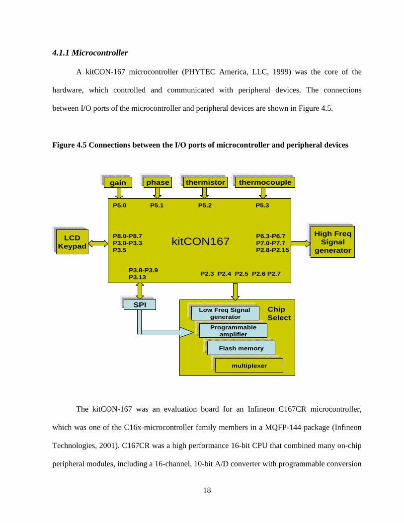
Figure 4.5 Connections between the I/O ports of microcontroller and peripheral devices
The kitCON-167 was an evaluation board for an Infineon C167CR microcontroller,
which was one of the C16x-microcontroller family members in a MQFP-144 package (Infineon
Technologies, 2001). C167CR was a high performance 16-bit CPU that combined many on-chip
peripheral modules, including a 16-channel, 10-bit A/D converter with programmable conversion
High FreqSignal
generator
LCDKeypad
SPI
gain
P6.3-P6.7P7.0-P7.7P2.8-P2.15
P8.0-P8.7P3.0-P3.3P3.5
P3.8-P3.9P3.13
P2.3 P2.4 P2.5 P2.6 P2.7
P5.0 P5.1 P5.2 P5.3
kitCON167
phase thermistor thermocouple
Low Freq Signal generator
Programmableamplifier
Flash memory
multiplexer
ChipSelect
High FreqSignal
generator
LCDKeypad
SPI
gain
P6.3-P6.7P7.0-P7.7P2.8-P2.15
P8.0-P8.7P3.0-P3.3P3.5
P3.8-P3.9P3.13
P2.3 P2.4 P2.5 P2.6 P2.7
P5.0 P5.1 P5.2 P5.3
kitCON167
phase thermistor thermocouple
Low Freq Signal generator
Programmableamplifier
Flash memory
multiplexer
ChipSelect
19
time of 7.8us, two 16-channel capture and compare units, 4-channel PWM units, two serial
channels, and a CAN interface with 15 message objects. C167CR can achieve 80/60 ns
instruction cycle time at 25/33 MHz CPU clock. The memory space of the C167CR was
configured in a Von Neumann architecture so that code memory, data memory, registers, and I/O
ports were organized within the same 16 MByte linear address space. C167CR has a 16-priority-
level interrupt system and up to 111 general purpose I/O lines, of which 47 I/O ports were used
in this study.
The kitCON-167 featured 256 kByte flash, 64 kByte SRAM and 512 Byte serial
EEPROM on the evaluation board. It allowed on-chip bootstrap loader, which was controlled by
a bit of an 8-bit DIP-switch. The DIP-switch on the evaluation board allowed executions of
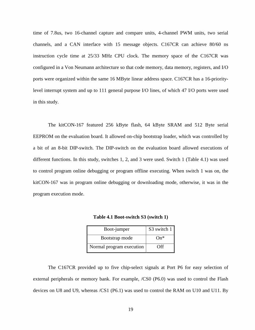
different functions. In this study, switches 1, 2, and 3 were used. Switch 1 (Table 4.1) was used
to control program online debugging or program offline executing. When switch 1 was on, the
kitCON-167 was in program online debugging or downloading mode, otherwise, it was in the
program execution mode.
Table 4.1 Boot-switch S3 (switch 1)
Boot-jumper S3 switch 1
Bootstrap mode On*
Normal program execution Off
The C167CR provided up to five chip-select signals at Port P6 for easy selection of
external peripherals or memory bank. For example, /CS0 (P6.0) was used to control the Flash
devices on U8 and U9, whereas /CS1 (P6.1) was used to control the RAM on U10 and U11. By
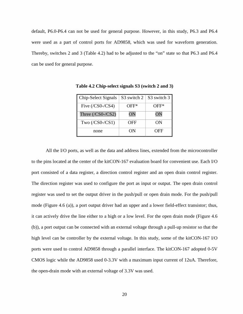
20
default, P6.0-P6.4 can not be used for general purpose. However, in this study, P6.3 and P6.4
were used as a part of control ports for AD9858, which was used for waveform generation.
Thereby, switches 2 and 3 (Table 4.2) had to be adjusted to the “on” state so that P6.3 and P6.4
can be used for general purpose.
Table 4.2 Chip-select signals S3 (switch 2 and 3)
Chip-Select Signals S3 switch 2 S3 switch 3
Five (/CS0-/CS4) OFF* OFF*
Three (/CS0-/CS2) ON ON
Two (/CS0-/CS1) OFF ON
none ON OFF
All the I/O ports, as well as the data and address lines, extended from the microcontroller
to the pins located at the center of the kitCON-167 evaluation board for convenient use. Each I/O
port consisted of a data register, a direction control register and an open drain control register.
The direction register was used to configure the port as input or output. The open drain control
register was used to set the output driver in the push/pull or open drain mode. For the push/pull
mode (Figure 4.6 (a)), a port output driver had an upper and a lower field-effect transistor; thus,
it can actively drive the line either to a high or a low level. For the open drain mode (Figure 4.6
(b)), a port output can be connected with an external voltage through a pull-up resistor so that the
high level can be controller by the external voltage. In this study, some of the kitCON-167 I/O
ports were used to control AD9858 through a parallel interface. The kitCON-167 adopted 0-5V
CMOS logic while the AD9858 used 0-3.3V with a maximum input current of 12uA. Therefore,
the open-drain mode with an external voltage of 3.3V was used.

21
Figure 4.6 Output Drivers in Push/Pull and Open Drain Modes
(a) Push/pull mode (b) Open drain mode
4.1.2 Signal generator
Two digital direct synthesizers were used for waveform generation. In order to increase
the frequency range, an AD9858 (Analog Devices, Inc., 2003a) evaluation board, which can
generate up to 400 MHz sinusoidal signals was adopted in this study. The output signal of the
AD9858 was found noisy at frequencies below 1 MHz. To solve this problem, another digital
direct synthesizer - AD9833 (Analog Devices, Inc., 2003b) - was used to generate sinusoidal
signals with frequencies below 1MHz.
4.1.2.1 Low frequency signal generator
An AD9833 was adopted for generating sine wave signals with frequencies below 1
MHz. The output frequency was software programmable. The frequency registers was 28 bits
and the frequency resolution was 0.1Hz. AD9833 needed a 25 MHz clock supplied to pin 5 -
MCLK (Figure 4.7).

22
Figure 4.7 Connection diagram of AD9833
Commands for AD9833 were written via a standard 3-wire serial interface compatible
with the SPI. The connection between AD9833 and kitCON-167 microcontroller is shown in
Figure 4.8. P3.9 and P3.13 on port P3 of the kitCON-167 were operated in alternate functions so
that port P3.9, which was Synchronous Serial Channel (SSC) with master transmit/slave receive
(MTSR), drove the serial data line SDATA. Port P3.13 (SCLK) was a clock signal, which was
set through the SSC Baud Rate register - SSCBR. The FSYNC pin was controlled by P2.6. When
data was ready to be transmitted to AD9833, P2.6 was set to low; otherwise, P2.6 was always
high.
Figure 4.8 Connections between kitCON-167 and AD9833
FSYNC
SDATA
SCLK
P2.6
MTSR
SCLK
kitCON167 AD9833
FSYNC
SDATA
SCLK
FSYNC
SDATA
SCLK
P2.6
MTSR
SCLK
P2.6
MTSR
SCLK
kitCON167 AD9833
The desired frequency of the analog output signal from AD9833 is determined by:
DESIREDf = 28/ 2MCLKf FREQTREG× (4.2)
23
where MCLKf =25 MHz, and
FREQTREG is the value loaded into the selected frequency register.
Thus, the value loaded into the selected frequency register can be derived from the
following equation:
FREQTREG = 282 /DESIRED MCLKf f× (4.3)
4.1.2.2 High frequency signal generator
An AD9858 DAC-output evaluation board was used for generating sine wave signals
with frequencies higher than 1 MHz. The AD9858 evaluation board had three functions: direct
digital synthesizer (DDS), analog mixer, and phase-locked loop (PLL). The latter two functions
were not used in this study. The AD9858 board can generate analog sine waves of up to 400MHz
when referenced to an external 1GHz clock input. The AD9858 also featured a divide-by-2 on
the clock input, allowing the external clock to be as high as 2GHz. In this study, a 1GHz
oscillator (Crystek Crystals Corporation, 2005) was used as an external reference clock. The
minimum output power of the oscillator was 10dBm. For the reference clock, the input
sensitivity was from -20dBm to +5dBm. Therefore, a 10dBm attenuator was connected to the
output of the 1GHz reference clock oscillator.
AD9858 featured a 32-bit frequency tuning word, allowing a fine tuning resolution. The
frequency tuning and control words can be loaded into the AD9858 via parallel (8-bit) or serial
communication format. In this study, parallel communication format was selected. The interface
consisted of 21 pins featuring an 8-bit data bus (D0-D7), a 6-bit address bus (A0-A5), RD, WR,

24
SPMODE, RESET, PS0, PS1 and FUD. The I/O port configuration of the kitCON167 for the
AD9858 is shown in Table 4.3.
Table 4.3 I/O port configuration of kitCON167 for AD9858
kitCON-167 I/O port Direction Pins on interface Function
P7.0-P7.7 Output D0-D7 Data bus
P2.8-P2.13 Output A0-A5 Address Bus
P2.14 Output WR Write bit
P2.15 Output RD Read Bit
P6.3 Output PS0 Profile select
P6.4 Output PS1 Profile select
P6.5 Output RESET Reset
P6.6 Output FUD Frequency update
P6.7 Output SPMODE Serial/Parallel communication
AD9858 had four user profiles (0-3), each of which can be selected by PS0 and PS1. The
user can load different frequency tuning words into different profiles. Each profile may have its
own frequency tuning word, which made it possible to change the frequency of the output signal
at a high speed. In this study, only one user profile was used. Thus, a new frequency needed to
be repeatedly written into the frequency tuning word register. The sine wave signal with the new
frequency was then produced by strobing the frequency update pin (FUD).
AD9858 had an integrated 10-bit current output DAC. The full-scale current IOUT was
determined by an external resistor (RSET) connected between the DACISET pin and the analog
ground. The relationship between the RSET and IOUT is:

25
39.19 /SET OUTR I= (4.4)
In order to provide the best spurious-free dynamic range performance, the AD9858
evaluation board limited the output to 20mA so that the value of RSET was 1.98K. By observing
output signals of AD9858, it was found that the amplitude of the output sinusoidal signal can
reach 1V at some frequencies. However, the gain and phase detector following the signal
generator allowed an input voltage range from -73dBV to -13dBV, which can be converted to
0.3 mV~ 320 mV. Therefore, the output amplitude of the AD9858 had to be attenuated to satisfy
the input range requirement of the next stage. In this study, the 1.98K resistor on the AD9858
evaluation board was replaced by a 6K resistor so that IOUT was reduced. The amplitude of the
output signal, which was controlled by IOUT, was then decreased to satisfy the input requirement
of the gain and phase detector.
4.1.3 Multiplexer
AD8186 (Analog Devices, Inc., 2003c) is a high speed, single-supply and triple 2-to-1
multiplexer (Figure 4.9). An AD8186 was used in this circuit to select from the two signal
generators, AD9833 and AD9858.
Figure 4.9 Pin Diagram of AD8186

26
In this circuit, only one of the three 2-to-1 channel was used. The output-enable control
pin (OE) was connected to a high level. An input was selected via the logic pin (SEL/A B ). The
input signal for IN0A or IN0B was selected when SEL/A B was set to high or low, respectively.
Both input and output of the AD8186 can swing to within ~1.3V of either rail. This
allowed the user 2.4V of dynamic range (1.3V~ 3.7V) for both input and output signals. For the
output signals from both signal generators, the amplitude was lower than 1.3V. Therefore, an
external reference voltage of 2.5V was applied to the VREF pin of AD8186. This reference
voltage raised the level of the input signal to satisfy the input requirement of AD8186. The 2.5V
reference voltage was provided by a micropower voltage reference diode LM185-2.5 (National
Semiconductor, 2008). Figure 4.10 is the schematic for the AD8186 multiplexer circuit.
Figure 4.10 Schematic for the AD8186 multiplexer circuit
IN0A1
DGND2
IN1A3
Vref4
IN2A5
Vcc6
Vee7
IN2B8
Vee9
IN1B10
Vee11
IN0B12 Vcc 13DVcc 14Vee 15OUT2 16Vcc 17OUT1 18Vee 19OUT0 20Vcc
21SEL A/B 22OE 23Vcc 24U4
AD8186
P2.7
Input signal H
GND
GND
C140.1uF
GND
C170.1uF
GND
C180.1uF
GND
C190.1uF
GND
5V
5V
5V5V
5V
R610KGND
C15
10uF
R74.99K
Vre
f
R5200K
R1010K
R810K
R114.99K
GND
9V
+ C1610uF
C320.1uF
C210.01uF
GNDGND
Vref
C22
0.1uF
GND Vre
f
+ C2010uF
GND
C240.1uF
+C2510uF
GND
5V
D1
LM185-2.5
Input Signal L
27
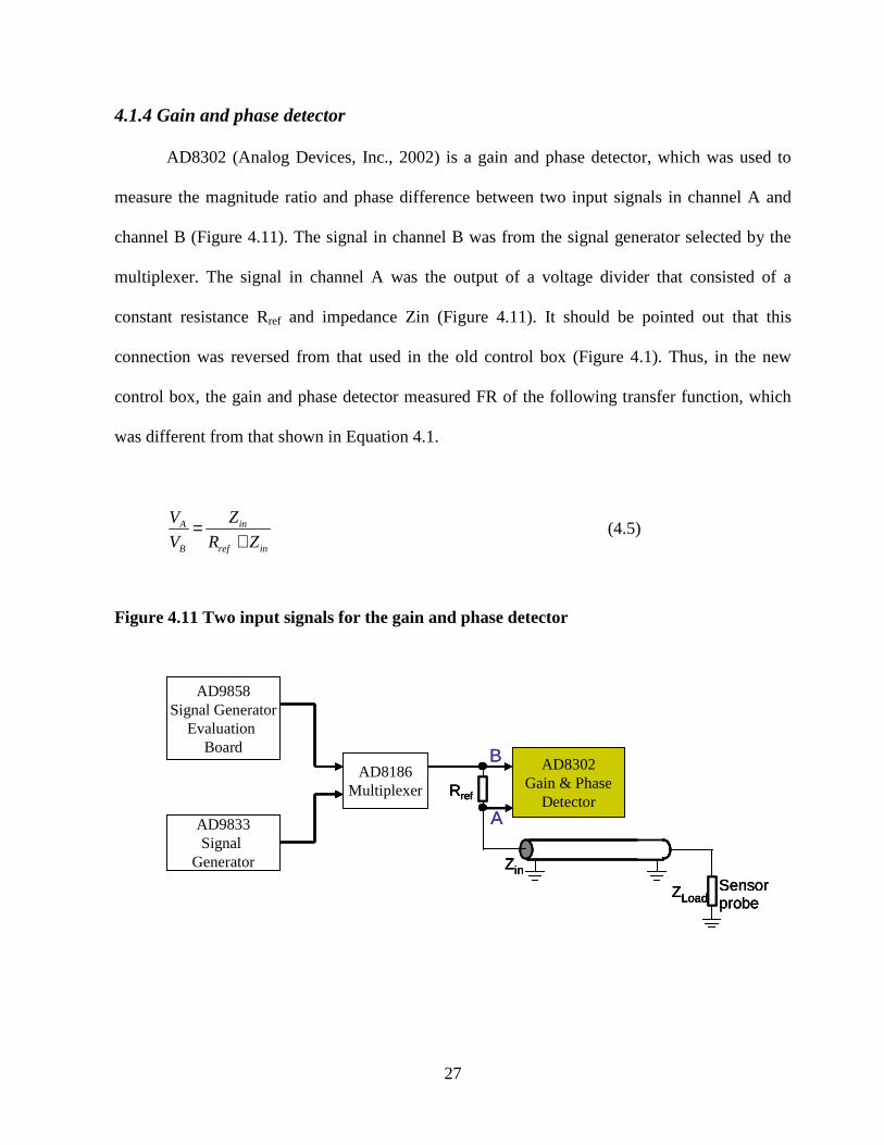
4.1.4 Gain and phase detector
AD8302 (Analog Devices, Inc., 2002) is a gain and phase detector, which was used to
measure the magnitude ratio and phase difference between two input signals in channel A and
channel B (Figure 4.11). The signal in channel B was from the signal generator selected by the
multiplexer. The signal in channel A was the output of a voltage divider that consisted of a
constant resistance Rref and impedance Zin (Figure 4.11). It should be pointed out that this
connection was reversed from that used in the old control box (Figure 4.1). Thus, in the new
control box, the gain and phase detector measured FR of the following transfer function, which
was different from that shown in Equation 4.1.
inA
B ref in
ZV
V R Z=
+ (4.5)
Figure 4.11 Two input signals for the gain and phase detector
Sensorprobe
AD8186Multiplexer
AD9858Signal Generator
Evaluation Board
AD9833Signal
Generator
AD8302Gain & Phase
Detector
ZLoad
Zin
Rref
A
B
Sensorprobe
AD8186Multiplexer
AD9858Signal Generator
Evaluation Board
AD9833Signal
Generator
AD8302Gain & Phase
Detector
ZLoad
Zin
Rref
Sensorprobe
AD8186Multiplexer
AD9858Signal Generator
Evaluation Board
AD9833Signal
Generator
AD8302Gain & Phase
Detector
ZLoad
Zin
Rref
AD8186Multiplexer
AD9858Signal Generator
Evaluation Board
AD9833Signal
Generator
AD8302Gain & Phase
Detector
ZLoad
Zin
Rref
A
B

28
The ac-coupled input signal of AD8302 can range from -60dBm to 0dBm in a 50 Ω
system, from low frequencies up to 2.7GHz. The output provided an accurate measurement of
gain over a ±30 dB range scaled to 30mV/dB, and the phase over a 0°-180° range scaled to
10mV/degree. The gain and phase output voltages were simultaneously available at ground
referenced outputs over the standard output range of 0 V to 1.8 V. The gain and phase output
voltages MAGV and PHSV can be calculated by:
log( / )MAG F SLP INA INB CPV R I V V V= + (4.6)
( ( ) ( ) 90 )PHS F INA INB CPV R I V V VΦ= − Φ − Φ − + (4.7)
where F SLPR I is 600mV/decade or 30mV/dB,
CPV is 900mV, and
FR IΦ is 10mV/degree.
For the gain function (Equation 4.6), a range of -30dB to +30dB covered the full-scale
swing from 0V to 1.8V, with a center point of 900mV for 0dB gain. For the phase function
(Equation 4.7), with a center point of 900mV for 90°, a range of 0° to 180° covers the full-scale
swing from 1.8 V to 0 V. The range of 0° to –180° covers the same full-scale swing but with the
opposite slope (Figure 4.12).

29
Figure 4.12 Idealized transfer characteristics for the gain and phase measurement mode
(Analog Devices, Inc., 2002)
The gain function (Equation 4.7) indicated that MAGV was determined by /INA INBV V . From
Figure 4.11, it can be seen that the amplitude of the signal sent to channel A was always lower
than that to channel B. Thus, the measured /INA INBV V would always be less than 1. As a result,
the measured magnitude ratio would be in the range of -30 dB to 0dB and MAGV would be in the
range of 0V to 900mV.
Configurations of the two single-ended inputs of AD8302 are identical. Each consists of a
driving pin (INPA or INPB), and an ac grounding pin (OFSA or OFSB) (Figure 4.13). For the
grounding pins, the coupling capacitor (C4 or C6) has two functions: it provides ac grounding and
sets the high-pass corner frequency for an internal offset compensation loop. An internal 10pF
capacitor sets the maximum corner frequency to approximately 200MHz. The corner can be
adjusted according the equation below:
30
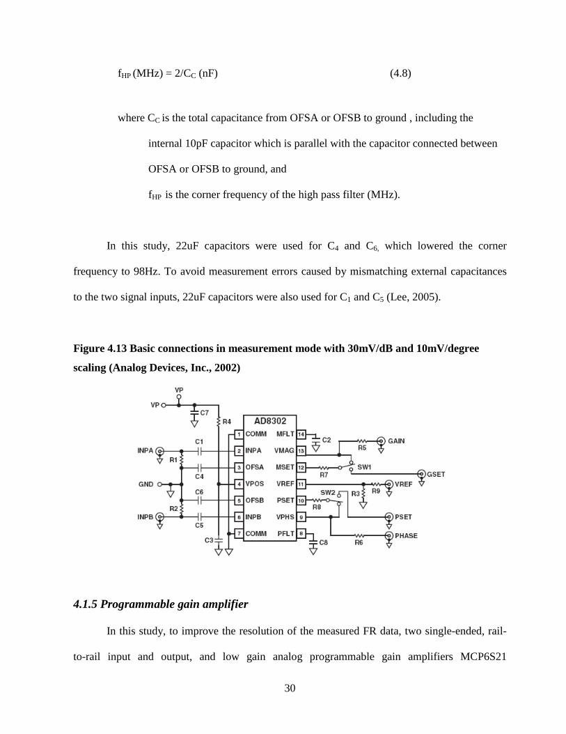
fHP (MHz) = 2/CC (nF) (4.8)
where CC is the total capacitance from OFSA or OFSB to ground , including the
internal 10pF capacitor which is parallel with the capacitor connected between
OFSA or OFSB to ground, and
fHP is the corner frequency of the high pass filter (MHz).
In this study, 22uF capacitors were used for C4 and C6, which lowered the corner
frequency to 98Hz. To avoid measurement errors caused by mismatching external capacitances
to the two signal inputs, 22uF capacitors were also used for C1 and C5 (Lee, 2005).
Figure 4.13 Basic connections in measurement mode with 30mV/dB and 10mV/degree
scaling (Analog Devices, Inc., 2002)
4.1.5 Programmable gain amplifier
In this study, to improve the resolution of the measured FR data, two single-ended, rail-
to-rail input and output, and low gain analog programmable gain amplifiers MCP6S21

31
(Microchip Technology Inc., 2003) (Figure 4.14) were used to amplify the magnitude ratio and
phase difference signals VMAG and VPHS, respectively. Reversing the input signals to the gain and
phase detector in the design of the new control box (Figure 4.11) from that of the old control box
(Figure 4.1) reduced the range of VMAG to 0-900mV, thus allowing the VMAG signal to be
amplified to achieve a higher resolution.
Figure 4.14 Pin connection diagram of MCP6S21 (Microchip Technology Inc., 2003)
In this study, MCP6S21 PGA used a standard SPI-compatible serial interface to receive
instructions from the kitCON-167 microcontroller (Figure 4.15). P3.9 and P3.13 on Port P3 of
the kitCON-167 microcontroller were operated in alternate functions so that port P3.9 (MTSR),
which was SSC with master transmit/slave receive, drove the serial data line SI. Port P3.13
(SCLK) was a clock signal, which was set through the register SSCBR. Ports P2.3 and P2.4 were
used for chip select.
Figure 4.15 Interface connections between kitCON-167 and MCP6S21
/CS
SI
SCK
P2.3/4
MTSR
SCLK
kitCON167 MCP6S21
/CS
SI
SCK
/CS
SI
SCK
P2.3/4
MTSR
SCLK
P2.3/4
MTSR
SCLK
kitCON167 MCP6S21

32
4.1.6 LCD and keypad
A keypad (Keypad16, Micro/Sys Inc., 2001) and a 2-line, 40-character LCD display
(LC0240, Micro/Sys Inc., 2001) were added to the system to allow users to enter commands and
to display the frequency response data with corresponding frequencies (Figure 4.16).
Figure 4.16 LCD and keypad
The LCD display and keypad were connected to an interface board (LCDKBD1,
Micro/Sys Inc.), which was powered by +5V. Both the LCD and keypad were controlled by 26
digital I/O lines from the kitCON-167 microcontroller through a ribbon cable. Of the 26 lines,
eight were used for a bi-directional data bus and five for additional control lines (Table 4.4). All
keys on the keypad are de-bounced (Wang 2002).
33
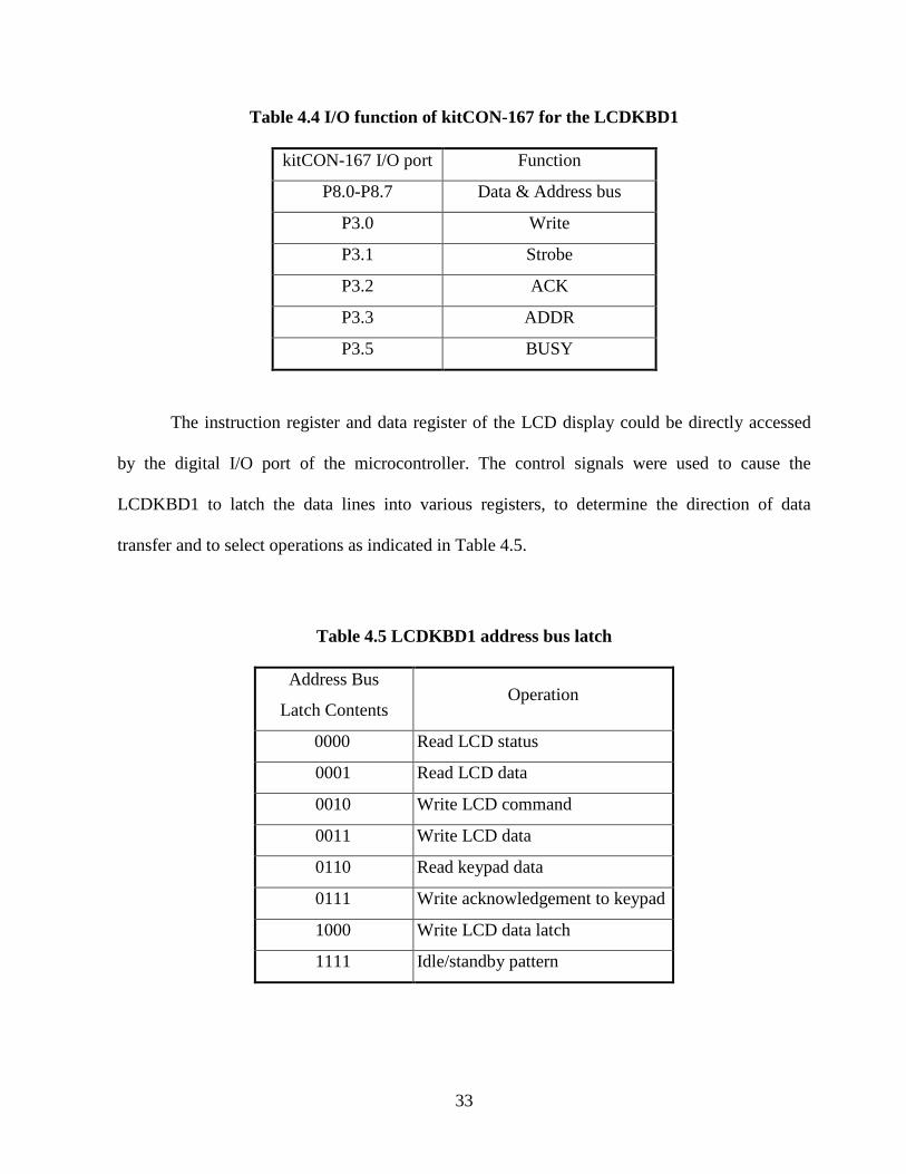
Table 4.4 I/O function of kitCON-167 for the LCDKBD1
kitCON-167 I/O port Function
P8.0-P8.7 Data & Address bus
P3.0 Write
P3.1 Strobe
P3.2 ACK
P3.3 ADDR
P3.5 BUSY
The instruction register and data register of the LCD display could be directly accessed
by the digital I/O port of the microcontroller. The control signals were used to cause the
LCDKBD1 to latch the data lines into various registers, to determine the direction of data
transfer and to select operations as indicated in Table 4.5.
Table 4.5 LCDKBD1 address bus latch
Address Bus
Latch Contents Operation
0000 Read LCD status
0001 Read LCD data
0010 Write LCD command
0011 Write LCD data
0110 Read keypad data
0111 Write acknowledgement to keypad
1000 Write LCD data latch
1111 Idle/standby pattern

34
4.1.7 Temperature measurement
The real-time temperature measurement module consisted of a thermistor, a type-T
thermocouple, and an amplifier. The thermistor was calibrated using a voltage divider formed by
the thermistor and a 10k resistor. The Steinhart-Hart equation (Equation 4.9) was used to obtain
the temperature from measured thermistor resistance. In order to determine the three coefficients
constant A, B and C, the thermistor was measured at three temperatures: icepoint (0°C), room
temperature (26°C), and boiling point (100°C).
31ln (ln )A B R C R
T= + + (4.9)
where R is the resistance of thermistor (Ω),
T is the temperature to be measured (K), and
A, B and C are the coefficients.
The type-T thermocouples used in this study were inexpensive, rugged and reliable. They
can be used over a wide temperature range from −200 to 350 °C. The temperature-emf
relationship of a thermocouple was not linear. For the type-T thermocouple, a 7th order
polynomial provided a good fit for this relationship (Equation 4.10).
2 7
0 1 2 7T a a x a x a x= + + + +… (4.10)
where x is measured emf (V),
T is the measured temperature (°C), and
0a =0.100860910, 1a =25727.94369, 2a =-767345.8295, 3a =78025595.81
4a =-9247486589, 5a =6.97688E+11, 6a =-2.66192E+13, 7a =3.94078E+14
35
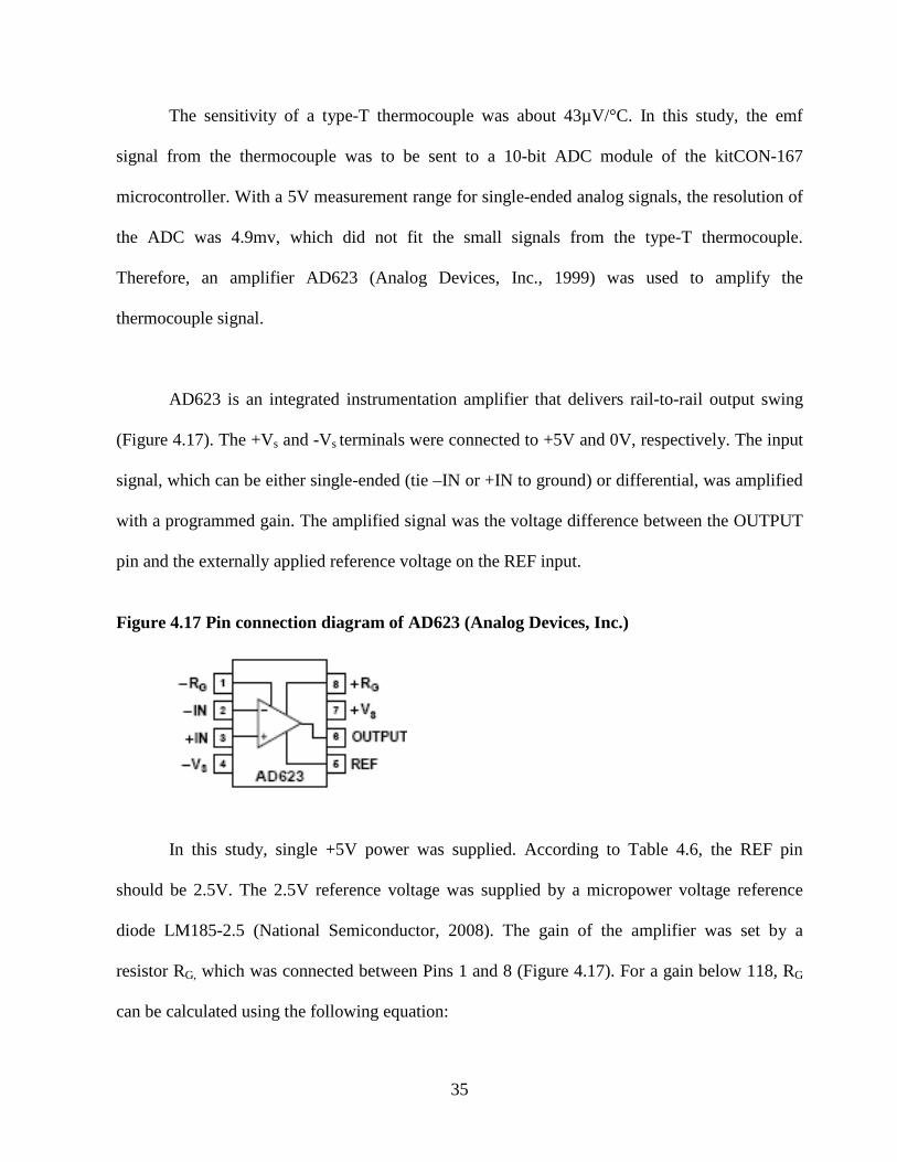
The sensitivity of a type-T thermocouple was about 43µV/°C. In this study, the emf
signal from the thermocouple was to be sent to a 10-bit ADC module of the kitCON-167
microcontroller. With a 5V measurement range for single-ended analog signals, the resolution of
the ADC was 4.9mv, which did not fit the small signals from the type-T thermocouple.
Therefore, an amplifier AD623 (Analog Devices, Inc., 1999) was used to amplify the
thermocouple signal.
AD623 is an integrated instrumentation amplifier that delivers rail-to-rail output swing
(Figure 4.17). The +Vs and -Vs terminals were connected to +5V and 0V, respectively. The input
signal, which can be either single-ended (tie –IN or +IN to ground) or differential, was amplified
with a programmed gain. The amplified signal was the voltage difference between the OUTPUT
pin and the externally applied reference voltage on the REF input.
Figure 4.17 Pin connection diagram of AD623 (Analog Devices, Inc.)
In this study, single +5V power was supplied. According to Table 4.6, the REF pin
should be 2.5V. The 2.5V reference voltage was supplied by a micropower voltage reference
diode LM185-2.5 (National Semiconductor, 2008). The gain of the amplifier was set by a
resistor RG, which was connected between Pins 1 and 8 (Figure 4.17). For a gain below 118, RG
can be calculated using the following equation:

36
100 /( 1)GR k G= Ω − (4.11)
In this study, RG was chosen as 1 k so that the gain was 101.
Table 4.6 Maximum attainable gain and resulting output swing for different input
conditions (Analog Devices, Inc., 1999)
4.1.8 Buffer amplifier
In this study, four voltage signals, including the gain and phase detector outputs, and
signals from the thermistor and the thermocouple, needed to be delivered to the ADC of the
kitCON-167 microcontroller. During circuit testing, it was found that the voltage signals
delivered at the ADC ports were always lower than those observed at the previous stage in the
signal conditioning circuit. For example, when the measured thermocouple signal at the output of
the amplifier AD623 was 2.510V, the voltage measured at port P5.3 of the ADC was 2.497V.
Similar reduction could be observed on other three voltage signals. This was probably caused by
the fact that the output impedances of the amplifiers were not sufficiently low and the input
impedance of the ADC module of kitCON167 was not sufficiently high. To solve this problem, a
voltage buffer TS925 (STMicroelectronics, 1999) was added on each ADC channel. TS925 is a
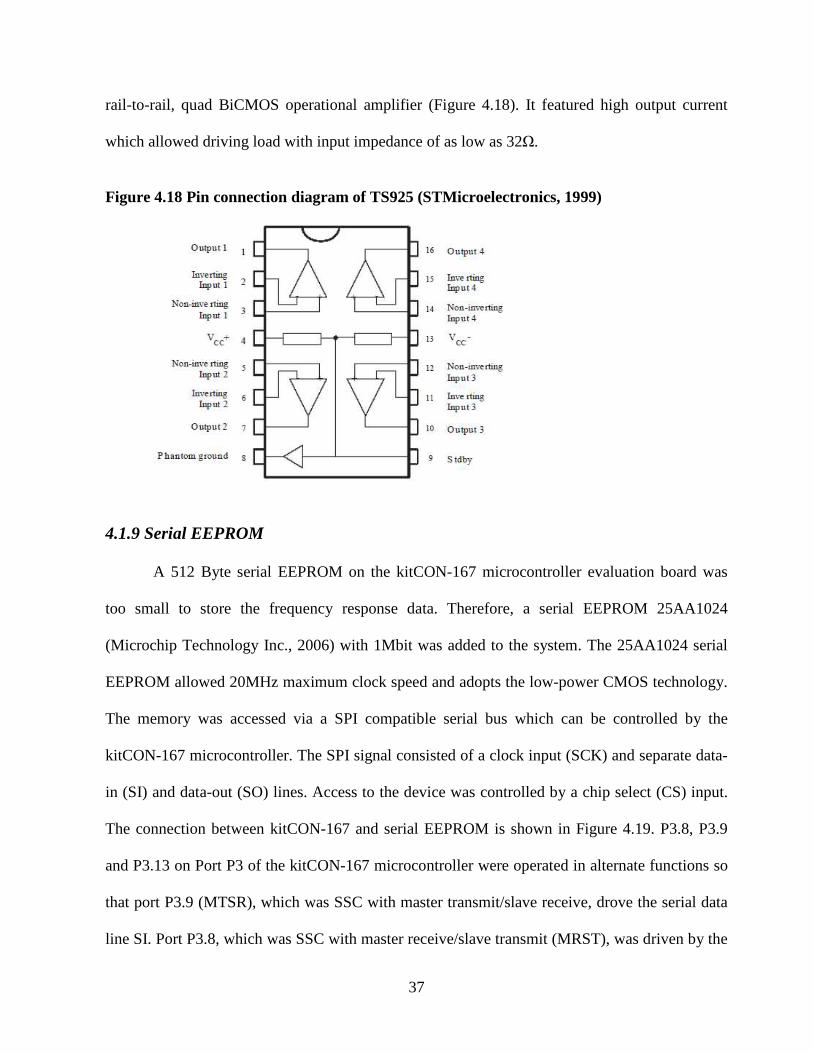
37
rail-to-rail, quad BiCMOS operational amplifier (Figure 4.18). It featured high output current
which allowed driving load with input impedance of as low as 32Ω.
Figure 4.18 Pin connection diagram of TS925 (STMicroelectronics, 1999)
4.1.9 Serial EEPROM
A 512 Byte serial EEPROM on the kitCON-167 microcontroller evaluation board was
too small to store the frequency response data. Therefore, a serial EEPROM 25AA1024
(Microchip Technology Inc., 2006) with 1Mbit was added to the system. The 25AA1024 serial
EEPROM allowed 20MHz maximum clock speed and adopts the low-power CMOS technology.
The memory was accessed via a SPI compatible serial bus which can be controlled by the
kitCON-167 microcontroller. The SPI signal consisted of a clock input (SCK) and separate data-
in (SI) and data-out (SO) lines. Access to the device was controlled by a chip select (CS) input.
The connection between kitCON-167 and serial EEPROM is shown in Figure 4.19. P3.8, P3.9
and P3.13 on Port P3 of the kitCON-167 microcontroller were operated in alternate functions so
that port P3.9 (MTSR), which was SSC with master transmit/slave receive, drove the serial data
line SI. Port P3.8, which was SSC with master receive/slave transmit (MRST), was driven by the
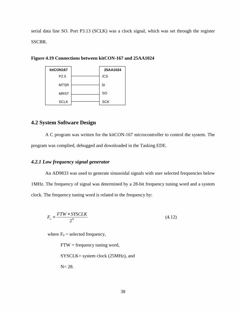
38
serial data line SO. Port P3.13 (SCLK) was a clock signal, which was set through the register
SSCBR.
Figure 4.19 Connections between kitCON-167 and 25AA1024
/CS
SI
SCK
P2.5
MTSR
SCLK
kitCON167 25AA1024
SOMRST
/CS
SI
SCK
P2.5
MTSR
SCLK
kitCON167 25AA1024
SOMRST
4.2 System Software Design
A C program was written for the kitCON-167 microcontroller to control the system. The
program was complied, debugged and downloaded in the Tasking EDE.
4.2.1 Low frequency signal generator
An AD9833 was used to generate sinusoidal signals with user selected frequencies below
1MHz. The frequency of signal was determined by a 28-bit frequency tuning word and a system
clock. The frequency tuning word is related to the frequency by:
2o N
FTW SYSCLKF
×= (4.12)
where F0 = selected frequency,
FTW = frequency tuning word,
SYSCLK= system clock (25MHz), and
N= 28.

39
AD9833 contains a 16-bit control register and two 28-bit frequency registers. Table 4.7
describes functions of the control bits. Table 4.8 is a description of the frequency register.
Table 4.7 Function of Control Bits of the control register in AD9833
(Analog Devices, Inc., 2003b)
Bit Name Function D15 0 D14 0
To inform the AD9833 that the contents of the control register will be altered, D15 and D14 must be set to 0.
D13 B28
B28=1 allows a complete word to be loaded into a frequency register in two consecutive writes. The first write contains the 14 LSBs of the frequency word, and the next the 14 MSBs. B28=0, the 28-bit frequency register operates as two 14-bit registers, one containing the 14 MSBs and the other 14 LSBs. The 14 MSBs of the frequency word can be altered independent of the 14 LSBs, and vice versa.
D12 HLB
This control bit allows the user to continuously load the MSBs or LSBs of a frequency register while ignoring the remaining 14 bits. D13 (B28) must be set to 0 to be able to change the MSBs and LSBs separately. When D13 (B28) =1, this control bit is ignored. HLB=1 allows a wirte to the 14 MSBs of the addressed frequency register HLB=0 allows a wirte to the 14 LSBs of the addressed frequency register
D11 FSELECT The bit defines whether the FREQ0 register or the FREQ1 register is used in the phase accumulator.
D10 PSELECT The bit defines whether the PHASE0 register or the PHASE1 register data is added to the output of the phase accumulator.
D9 Reserved This bit should be set to 0
D8 RESET RESET = 1 resets internal registers to 0, which corresponds to an analog output of midscale. RESET =0 disables RESET.
D7 SLEEP1 SLEEP1 =1, the internal MCLK clock is disabled, the DAC output will remain at its present value as the NCO is no longer accumulating. SLEEP1 =0, MCLK is enabled.
D6 SLEEP12 SLEEP12 = 1 powers down the on-chip DAC. SLEEP12 = 0 implies that the DAC is active.
D5 OPBITEN
This bit, in association with D1 (MODE), is to control what is output at the VOUT pin. When OPBITEN=1, the output of the DAC is no long available at the VOUT pin. Instead, the MSB (or MSB/2) of the DAC data is connected to the VOUT pin. When OPBITEN=0, the DAC is connected to VOUT. The MODE bit determines whether it is a sinusoidal or a ramp output.
D4 Reserved This bit must be set to 0.
D3 DIV2 DIV2 is used in association with D5 (OPBITEN) When DIV2=1, the MSB of the DAC data is passed directly to the VOUT pin When DIV2=0, the MSB/2 of the DAC data is output at the VOUT pin.
D2 Reserved This bit must be set to 0.
D1 MODE This bit is used in association with D5 (OPBITEN). When MODE=1, the output from the DAC is a triangle signal. When MODE=0, the output is a sinusoidal signal.
D0 Reserved This bit must be set to 0.
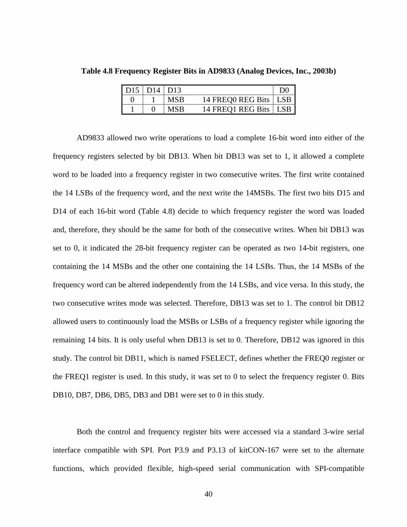
40
Table 4.8 Frequency Register Bits in AD9833 (Analog Devices, Inc., 2003b)
D15 D14 D13 D0 0 1 MSB 14 FREQ0 REG Bits LSB 1 0 MSB 14 FREQ1 REG Bits LSB
AD9833 allowed two write operations to load a complete 16-bit word into either of the
frequency registers selected by bit DB13. When bit DB13 was set to 1, it allowed a complete
word to be loaded into a frequency register in two consecutive writes. The first write contained
the 14 LSBs of the frequency word, and the next write the 14MSBs. The first two bits D15 and
D14 of each 16-bit word (Table 4.8) decide to which frequency register the word was loaded
and, therefore, they should be the same for both of the consecutive writes. When bit DB13 was
set to 0, it indicated the 28-bit frequency register can be operated as two 14-bit registers, one
containing the 14 MSBs and the other one containing the 14 LSBs. Thus, the 14 MSBs of the
frequency word can be altered independently from the 14 LSBs, and vice versa. In this study, the
two consecutive writes mode was selected. Therefore, DB13 was set to 1. The control bit DB12
allowed users to continuously load the MSBs or LSBs of a frequency register while ignoring the
remaining 14 bits. It is only useful when DB13 is set to 0. Therefore, DB12 was ignored in this
study. The control bit DB11, which is named FSELECT, defines whether the FREQ0 register or
the FREQ1 register is used. In this study, it was set to 0 to select the frequency register 0. Bits
DB10, DB7, DB6, DB5, DB3 and DB1 were set to 0 in this study.
Both the control and frequency register bits were accessed via a standard 3-wire serial
interface compatible with SPI. Port P3.9 and P3.13 of kitCON-167 were set to the alternate
functions, which provided flexible, high-speed serial communication with SPI-compatible
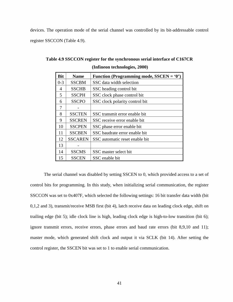
41
devices. The operation mode of the serial channel was controlled by its bit-addressable control
register SSCCON (Table 4.9).
Table 4.9 SSCCON register for the synchronous serial interface of C167CR
(Infineon technologies, 2000)
Bit Name Function (Programming mode, SSCEN = ‘0’) 0-3 SSCBM SSC data width selection 4 SSCHB SSC heading control bit 5 SSCPH SSC clock phase control bit 6 SSCPO SSC clock polarity control bit 7 - 8 SSCTEN SSC transmit error enable bit 9 SSCREN SSC receive error enable bit 10 SSCPEN SSC phase error enable bit 11 SSCBEN SSC baudrate error enable bit 12 SSCAREN SSC automatic reset enable bit 13 - 14 SSCMS SSC master select bit 15 SSCEN SSC enable bit
The serial channel was disabled by setting SSCEN to 0, which provided access to a set of
control bits for programming. In this study, when initializing serial communication, the register
SSCCON was set to 0x407F, which selected the following settings: 16 bit transfer data width (bit
0,1,2 and 3), transmit/receive MSB first (bit 4), latch receive data on leading clock edge, shift on
trailing edge (bit 5); idle clock line is high, leading clock edge is high-to-low transition (bit 6);
ignore transmit errors, receive errors, phase errors and baud rate errors (bit 8,9,10 and 11);
master mode, which generated shift clock and output it via SCLK (bit 14). After setting the
control register, the SSCEN bit was set to 1 to enable serial communication.

42
In this study, 25 frequencies were selected within the range of 200 Hz to 1 MHz: five
frequencies in a linear scale from 200 Hz to 1 kHz at 200Hz intervals, twenty frequencies in a
base-10 log scale from 1 kHz to 1 MHz. After the sine wave signal was generated at each
frequency, a wait command with a waiting period 100msec was issued to allow the generated
signals to be stabilized. The flow chart for AD9833 control is shown in Figure 4.20.
Figure 4.20 Flow chart for the AD9833 signal generator
InitializeCommunication
Initialization
Calculate the FTWfrom the desired frequency
Write two consecutive16-bit words to
frequency register
Apply reset bit
Writecontrol register
InitializeCommunication
Initialization
Calculate the FTWfrom the desired frequency
Write two consecutive16-bit words to
frequency register
Apply reset bit
Writecontrol register
4.2.2 High frequency signal generator
An AD9858 evaluation board was used to generate sinusoidal signals with user-selected
frequencies within the range of 1 MHz to 400 MHz. Frequencies of generated sinusoidal signals
were determined by a 32-bit frequency tuning word and a 1 GHz system clock. The desired
frequency was converted into the frequency tuning word (FTW), which can be written to the
FTW register followed by a frequency update. The relationship between the desired frequency

43
and the frequency tuning word was identical with that for the low frequency signal generator
AD9833 (Equation 4.12)
In this study, 499 frequencies were selected in a linear scale from 1.6 MHz to 400 MHz
with a 0.8 MHz interval. The waiting period between two frequencies was 100ms. AD9858 had
three modes of operation: single tone, frequency sweeping, and full sleep. In this study, the
single tone mode was used by programming frequency tuning word at parallel addresses from
0x0A to 0x0D (Table 4.10).
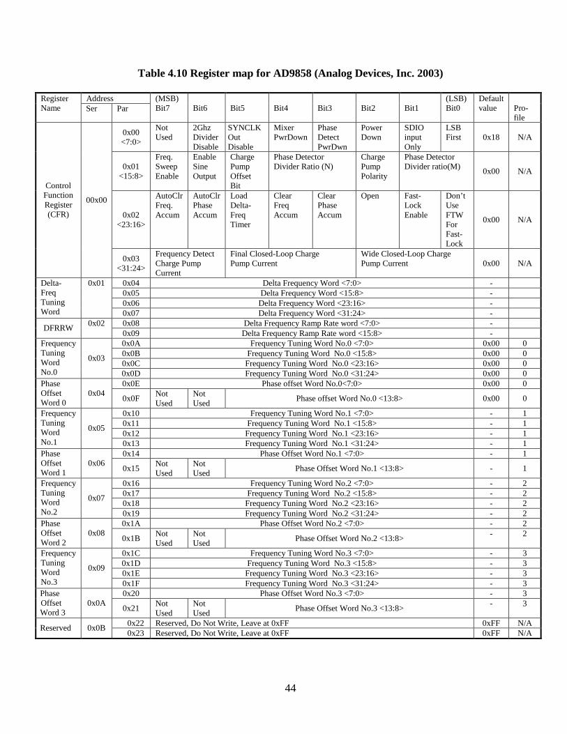
44
Table 4.10 Register map for AD9858 (Analog Devices, Inc. 2003)
Address Register Name Ser Par
(MSB) Bit7
Bit6
Bit5
Bit4
Bit3
Bit2
Bit1
(LSB) Bit0
Default value Pro-
file
0x00 <7:0>
Not Used
2Ghz Divider Disable
SYNCLK Out Disable
Mixer PwrDown
Phase Detect PwrDwn
Power Down
SDIO input Only
LSB First 0x18 N/A
0x01 <15:8>
Freq. Sweep Enable
Enable Sine Output
Charge Pump Offset Bit
Phase Detector Divider Ratio (N)
Charge Pump Polarity
Phase Detector Divider ratio(M)
0x00 N/A
0x02 <23:16>
AutoClr Freq. Accum
AutoClr Phase Accum
Load Delta- Freq Timer
Clear Freq Accum
Clear Phase Accum
Open Fast- Lock Enable
Don’t Use FTW For Fast- Lock
0x00 N/A
Control Function Register (CFR)
00x00
0x03 <31:24>
Frequency Detect Charge Pump Current
Final Closed-Loop Charge Pump Current
Wide Closed-Loop Charge Pump Current 0x00 N/A
0x04 Delta Frequency Word <7:0> - 0x05 Delta Frequency Word <15:8> - 0x06 Delta Frequency Word <23:16> -
Delta-Freq Tuning Word
0x01
0x07 Delta Frequency Word <31:24> - 0x08 Delta Frequency Ramp Rate word <7:0> -
DFRRW 0x02
0x09 Delta Frequency Ramp Rate word <15:8> - 0x0A Frequency Tuning Word No.0 <7:0> 0x00 0 0x0B Frequency Tuning Word No.0 <15:8> 0x00 0 0x0C Frequency Tuning Word No.0 <23:16> 0x00 0
Frequency Tuning Word No.0
0x03
0x0D Frequency Tuning Word No.0 <31:24> 0x00 0 0x0E Phase offset Word No.0<7:0> 0x00 0 Phase
Offset Word 0
0x04 0x0F
Not Used
Not Used
Phase offset Word No.0 <13:8> 0x00 0
0x10 Frequency Tuning Word No.1 <7:0> - 1 0x11 Frequency Tuning Word No.1 <15:8> - 1 0x12 Frequency Tuning Word No.1 <23:16> - 1
Frequency Tuning Word No.1
0x05
0x13 Frequency Tuning Word No.1 <31:24> - 1 0x14 Phase Offset Word No.1 <7:0> - 1 Phase
Offset Word 1
0x06 0x15
Not Used
Not Used
Phase Offset Word No.1 <13:8> - 1
0x16 Frequency Tuning Word No.2 <7:0> - 2 0x17 Frequency Tuning Word No.2 <15:8> - 2 0x18 Frequency Tuning Word No.2 <23:16> - 2
Frequency Tuning Word No.2
0x07
0x19 Frequency Tuning Word No.2 <31:24> - 2 0x1A Phase Offset Word No.2 <7:0> - 2 Phase
Offset Word 2
0x08 0x1B
Not Used
Not Used
Phase Offset Word No.2 <13:8> - 2
0x1C Frequency Tuning Word No.3 <7:0> - 3 0x1D Frequency Tuning Word No.3 <15:8> - 3 0x1E Frequency Tuning Word No.3 <23:16> - 3
Frequency Tuning Word No.3
0x09
0x1F Frequency Tuning Word No.3 <31:24> - 3 0x20 Phase Offset Word No.3 <7:0> - 3 Phase
Offset Word 3
0x0A 0x21
Not Used
Not Used
Phase Offset Word No.3 <13:8> - 3
0x22 Reserved, Do Not Write, Leave at 0xFF 0xFF N/A Reserved 0x0B
0x23 Reserved, Do Not Write, Leave at 0xFF 0xFF N/A

45
A flow chart for the section of the control program that generates 499 frequencies using
the AD9858 signal generator is shown in Figure 4.21.
Figure 4.21 Flow chart for the AD9858 signal generator
InitializeI/O port
Initializecontrol register
Calculate the FTWfrom the desired frequency
Write FTW data tothe FTW register
Frequency update
InitializeI/O port
Initializecontrol register
Calculate the FTWfrom the desired frequency
Write FTW data tothe FTW register
Frequency update
4.2.3 A/D module
The C167CR microcontroller provided an Analog/Digital Converter with 10-bit
resolution and an on-chip sample & hold circuit, which can be accessed via Port 5 set to the
alternate functions. The analog data from the outputs of the gain and phase detector were sent to
the A/D converter in the “auto scan, single conversion mode”, which automatically converted a
sequence of analog signals beginning at port P5.3 and ending at P5.0. The converted data were
recorded when an interrupt request flag was set high at the end of A/D conversion. The result of
a conversion was stored in bit field ADRES of the 16-bit result register ADDAT, as shown in
Table 4.11. The higher four bits of the register ADDAT (CHNR) are used to identify the analog
channels.

46
Table 4.11 ADC result register of C167CR (Infineon technologies, 2000)
Bit Name Function
0-9 ADRES A/D conversion result
The 10-bit digital result of the most recent conversion.
10 -
11 -
12-15 CHNR Channel number (identifies the converted analog channel)
4.2.4 Programmable gain amplifier
To improve the resolution of measured FR data, two programmable gain amplifiers
MCP6S21 were used to amplify the outputs of the gain and phase detector. The amplifiers were
controlled via standard, SPI compatible serial communication. The communication initialization
was similar to that for the low frequency signal generator (Section 4.2.1). The amplifiers were
programmed using a 16-bit word, which was sent into the amplifier through the pin (SI) of
MCP6S21 (Section 4.1.5). The first byte of the 16-bit word was the instruction byte, which went
into the instruction register. The second byte was determined by the indirect address bit A0 in the
instruction register (Table 4.12).
Table 4.12 Instruction register of MCP6S21 (Microchip Technology Inc., 2003)
Bit Name Function
Bit 7 M2
Bit 6 M1
Bit 5 M0
M2-M0 are the command bits that determine the following functions:
000=NOP (Default); 001= PGA enters Shutdown Mode once a full 16-bit word
is sent and /CS is raised; 010= Write to register; 011 and 1xx= NOP
Bit 4 - Bit 3 - Bit 2 - Bit 1 -
Unimplemented: read as 0
Bit 0 A0 A0 is the indirect Address Bit: 1=Addresses the Channel Register 0=Addresses the Gain Register (Default)

47
In this study, bits M2 to M0 were assigned 001, which let the program gain amplifier
enter the shutdown mode as soon as a full 16-bit word is sent and the chip select pin (/CS) is set
to high. The shutdown mode puts the amplifier to a low power mode. In this mode, the internal
registers maintain their values until either a valid command is sent to the device or the device is
powered down and backed up again. Bit A0 was set to 0 so that the second byte of the 16-bit
word goes to the gain register (Table 4.13).
Table 4.13 Gain register of MCP6S21 (Microchip Technology Inc., 2003)
— — — — — G2 G1 G0
bit 7 bit 0
In the gain register, bits G2 to G0 are gain select bit to define the gain whereas bits 3 to 7
were not used. The gain of the amplifier can be set between +1V/V and +32V/V through
programming bits G0 - G2 (Table 4.14).
Table 4.14 Gain selected bits of MCP6S21 (Microchip Technology Inc., 2003)
G2 G1 G0 Gain
0 0 0 1
0 0 1 2
0 1 0 4
0 1 1 5
1 0 0 8
1 0 1 10
1 1 0 16
1 1 1 32
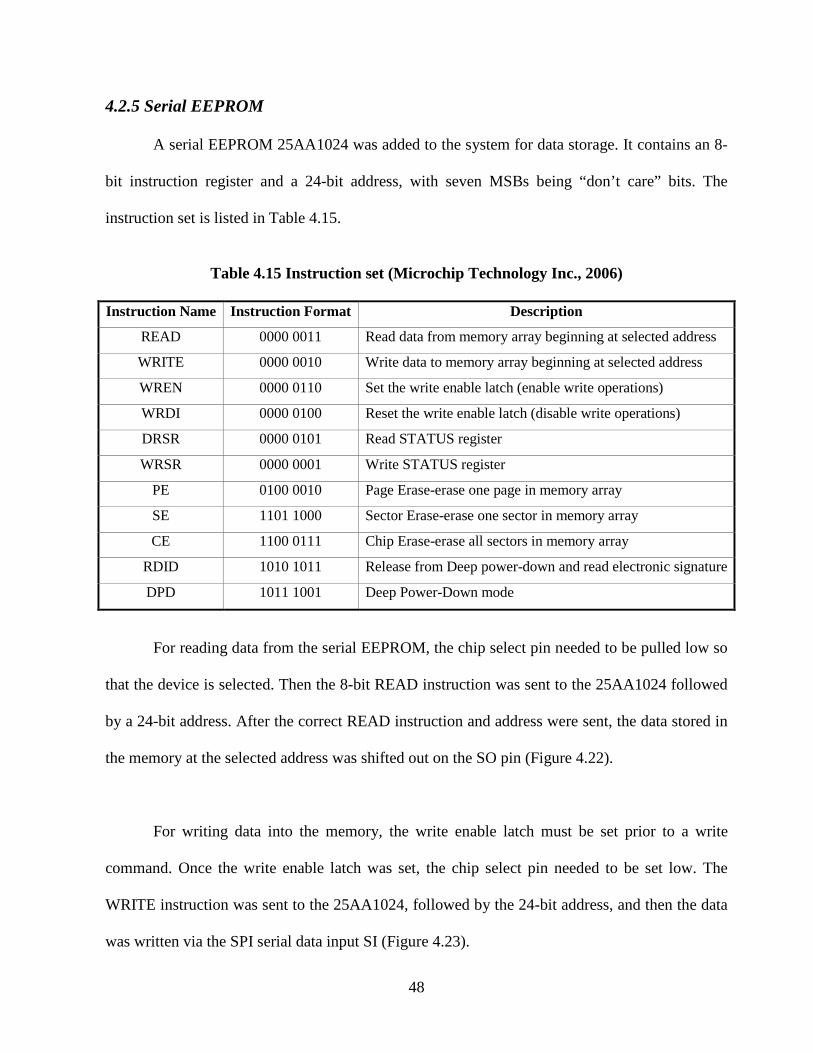
48
4.2.5 Serial EEPROM
A serial EEPROM 25AA1024 was added to the system for data storage. It contains an 8-
bit instruction register and a 24-bit address, with seven MSBs being “don’t care” bits. The
instruction set is listed in Table 4.15.
Table 4.15 Instruction set (Microchip Technology Inc., 2006)
Instruction Name Instruction Format Description
READ 0000 0011 Read data from memory array beginning at selected address
WRITE 0000 0010 Write data to memory array beginning at selected address
WREN 0000 0110 Set the write enable latch (enable write operations)
WRDI 0000 0100 Reset the write enable latch (disable write operations)
DRSR 0000 0101 Read STATUS register
WRSR 0000 0001 Write STATUS register
PE 0100 0010 Page Erase-erase one page in memory array
SE 1101 1000 Sector Erase-erase one sector in memory array
CE 1100 0111 Chip Erase-erase all sectors in memory array
RDID 1010 1011 Release from Deep power-down and read electronic signature
DPD 1011 1001 Deep Power-Down mode
For reading data from the serial EEPROM, the chip select pin needed to be pulled low so
that the device is selected. Then the 8-bit READ instruction was sent to the 25AA1024 followed
by a 24-bit address. After the correct READ instruction and address were sent, the data stored in
the memory at the selected address was shifted out on the SO pin (Figure 4.22).
For writing data into the memory, the write enable latch must be set prior to a write
command. Once the write enable latch was set, the chip select pin needed to be set low. The
WRITE instruction was sent to the 25AA1024, followed by the 24-bit address, and then the data
was written via the SPI serial data input SI (Figure 4.23).

49
Figure 4.22 Read sequence of 25AA1024 (Microchip Technology Inc., 2006)
Figure 4.23 Byte write sequence of 25AA1024 (Microchip Technology Inc., 2006)
4.2.6 Microcontroller
A C program in machine-readable format was downloaded to the flash memory of
kitCON-167 microcontroller using the FlashTools 16W via serial interface. The program was set
to run three times for each measurement. The measured FR data were delivered to a PC through
RS232 serial interface. The HyperTerminal tool available under the windows operation system
was responsible for accepting the data and saving it in text files in the PC. The flow chart for
control program written for the kitCON-167 microcontroller is shown in Figure 4.24.

50
Figure 4.24 Flow chart of the microcontroller program

51
Freq_index<50 ? Freq_index<55 ? Freq_index<75 ? Freq_index<574 ?
Freq=Freq_indexFreq=200*(Freq
_index-49)
Freq
=100(0.15*(Freq_index-54)+3)Freq=800000(Freq_ind
ex-74)+800000
Freq_index>=50 ?
Freq<=1000000 ?
Call low frequency
generator subroutine
Wait 100msec
Call high frequency
generator subroutine
Collect data
Are freq_index>50 and
freq_index%10=0 ?
Display frequency,
magnitude ratio, phase
difference digital value
Clear LCD
N
Y
NN
YYY
Y
N
Y
N
1 2
Y
N
52
CHAPTER 5 - Impedance Transformation Models
Permittivity is a property of dielectric materials. Permittivity relates to a material’s
ability to conduct AC currents. When a probe is immersed in a dielectric material, the
permittivity and corresponding admittance of the probe becomes a measure of how easily a
current can flow through the dielectric material within the probe. Thus, permittivity of the
dielectric material can be found by measuring the admittance of a probe immersed in the material
and then removing the geometric factor. Impedance is the reciprocal of admittance and,
therefore, permittivity of the dielectric material also can be found by measuring the impedance of
the probe immersed in the material and then removing the geometric factor.
In this study, impedance of the sensor probe was derived from measured FR data. To
study the probe impedance, impedance transformation models for the sensor probe, the coaxial
cable that connects the control system with the sensor probe and the signal processing circuit
were investigated.
5.1 Transmission line theory
5.1.1 Introduction of transmission line theory
A transmission line is used to guide energy in the form of electromagnetic waves,
acoustic waves, or electric power, from the source to the receiver. In many electric circuits,
transmission wires connecting various components can be generally neglected, because the
voltage at each point along the wire can be considered identical at a given time due to the short

53
lengths of the wires. However, if the wires are sufficiently long and the frequency is sufficiently
high so that voltages along the wire at a given time can no longer be considered identical, the
transmission line becomes important (Coleman, 2004). A rule-of-thumb commonly used is that,
when the length of a wire is greater than 1/10 of the wavelength, the wire should be treated as a
transmission line. If a design ignores the transmission line effect when it should be considered,
signal reflection along the wires and cables would result in significant variations in the
impedance present at different points on the line. In the transmission line theory, models for
coaxial cables and twin parallel wires are the most common models in circuit analysis. In this
study, a coaxial cable connecting the control box with the permittivity sensor probe was studied.
5.1.2 Coaxial cable
Coaxial cables (C1166 RG 58/U) of different lengths were used to connect the control
box with the sensor probe. The shortest cable used in this study was 33cm. The highest
frequency of the signal from the signal generator was 400 MHz. One tenth of its wavelength was
5cm after accounting for a relative propagation velocity of 0.66. Therefore, it was necessary to
study the transmission line losses along the cable.
To simplify the analysis, a coaxial cable can be considered as a distribution of discrete
capacitances and inductances, as shown in Figure 5.1.
Figure 5.1 Distributed impedance model for a transmission line (Coleman, 2004)
C
L

54
The inductances and capacitances in Figure 5.1 can be determined by Equation 5.1 and
5.2, respectively.
ln( )2
bL
a
µπ
= (5.1)
2
ln( )C
b
a
πε= (5.2)
where L is the inductance per unit length of the cable,
C is the capacitance per unit length of the cable,
ε is the permittivity of the medium between the conductors,
µ is the permeability of the medium between the conductors,
b is the outer diameter of the cable, and
a is the inner diameter of the cable.
The characteristic impedance of the transmission line can be derived from the inductance
and capacitance per unit length of the cable.
0LZ C= (5.3)
where Z0 is the characteristic impedance of the transmission line

55
For a transmission line of length l terminated with a load, if a sinusoidal with voltage V+
is launched into an end of the line, a portion of the power will be absorbed by the load and the
remaining power will be reflected back through the line. The voltage of the reflected sinusoidal
can be expressed by:
V V− += Γ (5.4)
where V+ is the input voltage,
V- is the reflected voltage, and
Γ is the reflection coefficient.
In Equation 5.4, all quantities are complex. Thus, both phase changes and amplitude information
are included.
The reflection coefficient LΓ at a general load ZL can be acquired by:
0
0
LL
L
Z Z
Z Z
−Γ =+
(5.5)
where LΓ is the reflection coefficient at a general load ZL, and
ZL is the impedance of the load.
Power will not be reflected back when LΓ = 0. Under this condition, LZ = 0Z , and the
load is said to be matched to the line. However, in general, LZ ≠ 0Z and a portion of the signal is
reflected. Moreover, due to phase variation along the line, which is caused by time delays in
signal propagation, the ratio of V- to V+ changes in phase. Thus, the reflection coefficient
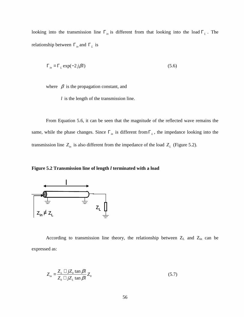
56
looking into the transmission line inΓ is different from that looking into the loadLΓ . The
relationship between inΓ and LΓ is
exp( 2 )in L j lβΓ = Γ − (5.6)
where β is the propagation constant, and
l is the length of the transmission line.
From Equation 5.6, it can be seen that the magnitude of the reflected wave remains the
same, while the phase changes. Since inΓ is different from LΓ , the impedance looking into the
transmission line inZ is also different from the impedance of the load LZ (Figure 5.2).
Figure 5.2 Transmission line of length l terminated with a load
ZLZin = ZL
l
ZLZin = ZL
l
According to transmission line theory, the relationship between ZL and Zin can be
expressed as:
00
0
tan
tanL
inL
Z jZ lZ Z
Z jZ l
ββ
+=+
(5.7)
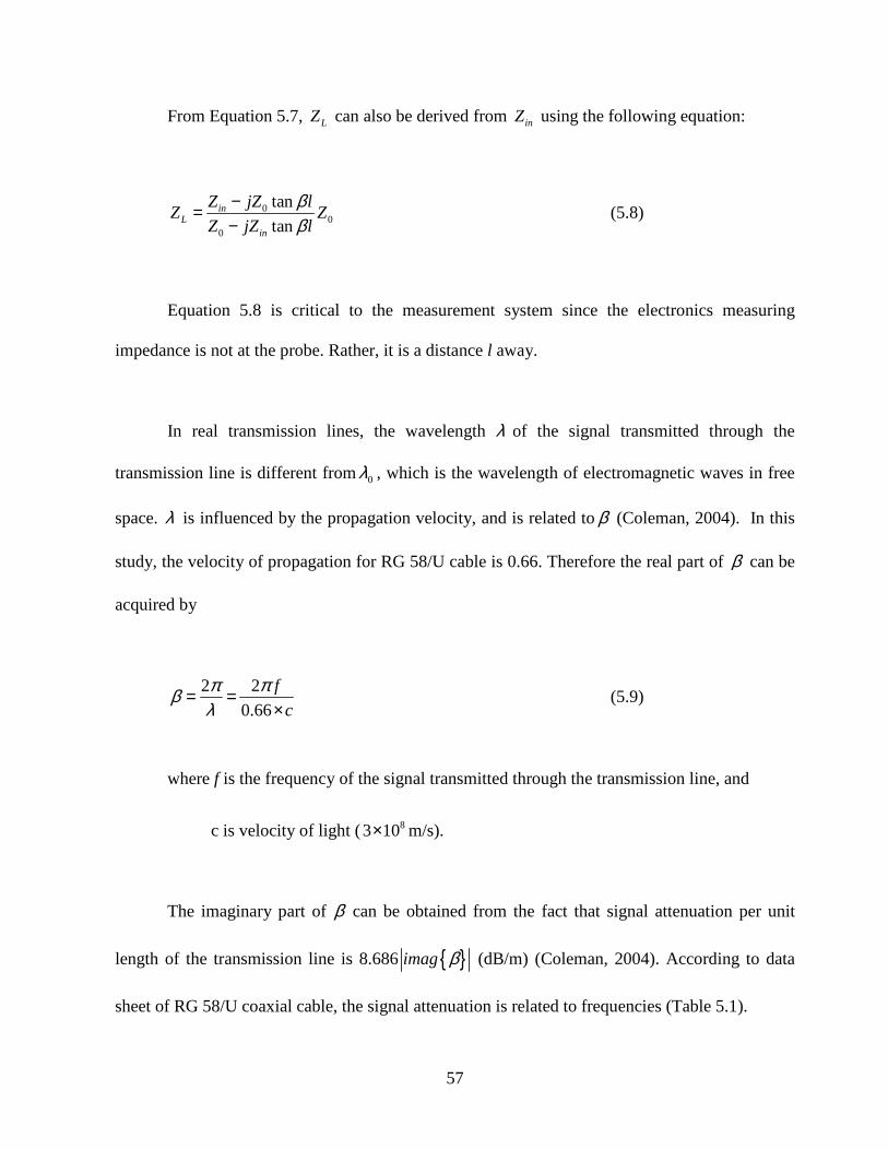
57
From Equation 5.7, LZ can also be derived from inZ using the following equation:
00
0
tan
tanin
Lin
Z jZ lZ Z
Z jZ l
ββ
−=−
(5.8)
Equation 5.8 is critical to the measurement system since the electronics measuring
impedance is not at the probe. Rather, it is a distance l away.
In real transmission lines, the wavelength λ of the signal transmitted through the
transmission line is different from0λ , which is the wavelength of electromagnetic waves in free
space. λ is influenced by the propagation velocity, and is related toβ (Coleman, 2004). In this
study, the velocity of propagation for RG 58/U cable is 0.66. Therefore the real part of β can be
acquired by
2 2
0.66
f
c
π πβλ
= =×
(5.9)
where f is the frequency of the signal transmitted through the transmission line, and
c is velocity of light ( 83 10× m/s).
The imaginary part of β can be obtained from the fact that signal attenuation per unit
length of the transmission line is 8.686 imag β (dB/m) (Coleman, 2004). According to data
sheet of RG 58/U coaxial cable, the signal attenuation is related to frequencies (Table 5.1).
58
Table 5.1 Signal attenuation in coaxial cable C1166 RG 58/U
Frequency (MHz) 1 10 50 100 200 500 1000
Attenuation (dB/100') 0.40 1.20 2.90 4.20 6.00 10.17 16.50
Attenuation (dB/m) 0.01312 0.03937 0.09514 0.1378 0.1969 0.33371 0.5413
Several regression models, including a linear model, a polynomial model, and a power
model, were developed based on the data shown in Table 5.1 to predict signal attenuations in the
cable at various frequencies. The result showed that the power model had the highest R2 value of
0.9975 (Figure 5.3). Therefore, the power model was used to calculate the attenuation.
Figure 5.3 Models for attenuation per unit length for the coaxial cable C1166 RG 58/U
y = 0.0005x + 0.0604
R2 = 0.9712
y = -3E-07x2 + 0.0008x + 0.0414
R2 = 0.9885
y = 0.0122x0.5342
R2 = 0.9975
0
0.1
0.2
0.3
0.4
0.5
0.6
1 10 100 1000
Frequency(MHz)
Atte
nuat
ion(
dB/m
)
Attenuation linear prediction
poly prediction power prediction
5.2 Sensor probe model
The sensor probe consisted of six aluminum plates placed in parallel, with identical
spacing between adjacent plates. Two sensor probes with different size are shown in Figure 5.4.

59
The larger probe (Figure 5.4 (a)) was 7.5cm×3.5cm in size, with 4mm spacing. The smaller
probe (Figure 5.4 (b)) was 5cm ×3.5cm in size, with 4mm spacing. In this thesis, these probes
will be referred to as the “7.5cm” and “5cm” probes, respectively.
Figure 5.4 Sensor probes
(a) The 7.5cm probe (b) The 5cm probe
On each probe, alternating plates were electrically connected to form a capacitor that
looks similar to the old-fashioned air capacitor. Because each pair of adjacent plates forms a
simple two-plate capacitor, the six plates on the probe form five capacitors in a parallel
connection. Thus, the total capacitance of the probe can be estimated as:
'05 5L
A AC
d dε ε ε= ⋅ ⋅ = ⋅ ⋅ (5.10)
where C is the capacitance (F),
A is the area of each plate (m2),

60
'ε is the dielectric constant of the material,
0ε is the permittivity of free space (8.854*10-12 F/m), and
d is the spacing between adjacent plates (m).
When the probe is immersed in a dielectric medium, a part of the imaginary component
of the permittivity of the medium (Equations 3.2 and 3.3) between adjacent plates also forms a
parallel resistor. Due to the alternating electric connections among the plates, the total resistance
of the probe can be viewed as a parallel connection of five identical resistors. Thus, the total
resistance of the probe can be estimated as:
1
5L
dR
A
ρ⋅= ⋅ (5.11)
where A is the area of each plate (m2), and
ρ is the resistivity of the material.
With both capacitive and resistive effects considered, the probe can be viewed as a
parallel connection of CL and RL. Thus, the total impedance of the probe can be expressed as:
1
//1 1
LL L
L R CL L
LL
Rj C R
Z Z Zj C RR
j C
ωω
ω
⋅= = =
++ (5.12)
where ω is the angular frequency of the external electric field.

61
5.3 Circuit model
The signal processing circuit in the new control box was different from that in the old
control box. Thus, the circuit models for FR measurement were investigated for the new and old
control boxes, respectively.
5.3.1 Circuit model for the new control box
The circuit schematic for FR measurement using the new control box is shown in Figure
5.5. The circuit consisted of three parts: part A is for analog-to-digital conversion, part B is for
the transformation between the input and output signals of the gain and phase detector, and part
C is for impedance transformation between the input signals of the gain and phase detector, V3
and V4 , and Zin.
The parallel connection of R3 (3kΩ) and C2 (2pF) in part B is the input impedance of the
gain and phase detector. In part C, C1 is a ceramic capacitor of 22uF; both Rref and R2 are thin
film chip resistors of 50 Ω.
Figure 5.5 Circuit schematic for FR measurement using the new control box
R33k
R33k
R250
R250
Rref50
C22pF
C2
2pF
C1
22uF
C1
22uF
GND
GND GND
GND
VMAGINPA
INPB
VPHS
Sig
Gen
V1
V2 V3
V4
Sensorprobe
ZL Zin
Gain and
phase
detector
Amplifier
ADmodule
Amplifier
P5.0
P5.1
DMAG
DPHS
ABC
R33k
R33k
R250
R250
Rref50
C22pF
C2
2pF
C1
22uF
C1
22uF
GND
GND GND
GND
VMAGINPA
INPB
VPHS
Sig
Gen
V1
V2 V3
V4
Sensorprobe
ZL Sensorprobe
ZL Zin
Gain and
phase
detector
Amplifier
ADmodule
Amplifier
P5.0
P5.1
DMAG
DPHS
ABC
62
For part A, the two outputs VMAG and VPHS of the gain and phase detector can be derived
from the measured FR data DMAG and DPHS, respectively. Assuming the gain of each amplifier is
M and N, respectively, VMAG and VPHS can be calculated as:
( 5000 /1024) /MAG MAGV D M= × (5.13)
( 5000 /1024) /PHS PHSV D N= × (5.14)
For part B, the relationship between the input signals, V3 and V4, and the output signals,
VMAG and VPHS, of the gain and phase detector can be acquired based on Equation 4.6 and 4.7
(Section 4.1.4):
3
420log / 30 30MAG
V VV = − (5.15)
3 4( ) ( ) /10 180PHSV V VΦ − Φ = − (5.16)
Therefore, 3
4
VV can be derived from the following equation:
3 3 33 4 3 4
4 4 4cos( ( ) ( )) sin( ( ) ( ))V V VV V j V VV V V= Φ − Φ + Φ − Φ (5.17)
For part C, the goal of modeling was to express Zin as a function3
4
VV . To achieve this
goal, several impedances in the transmission paths need to be defined.

63
3 2
332
3 23
2
1
1 1R C
RRj C
Zj R CR
j C
ωω
ω
⋅= =
++ (5.18)
where 3 2R CZ is the total parallel impedance of R3 and C2.
1
1
1CZ
j Cω= (5.19)
where1CZ is the impedance of C1.
The relationship between V2 and V3, V1 and V4 can be expressed as follows:
3 2 3 2 1
3 2
R C R C C
V V
Z Z Z=
+ (5.20)
3 2 3 2 1
4 1
R C R C C
V V
Z Z Z=
+ (5.21)
where V1 is the signal from the signal generator, and
V2 is the signal measured at the Zin end of the cable that connects the control box
and the sensor probe. It can also be viewed as output of a voltage divider that
consisted of resistor R1 and impedance Zin
The following equation can be derived by combining Equations 5.20 and 5.21.

64
3 2
4 1
V V
V V= (5.22)
Applying the Kirchhoff’s current law to the Zin end of the cable, the relationship between
V1 and V2 can be expressed by:
3 2 1
1 2 2 2 2
2ref in R C C
V V V V V
R Z R Z Z
− = + ++
(5.23)
Therefore, Zin can be expressed as:
3 2 1
1
2 21( )
refin
ref ref
R C C
RZ
R RVV R Z Z
=− − −+
(5.24)
By substituting equation 5.22 into 5.24, Zin can be estimated from the two input signals,
V3 and V4, of the gain and phase detector.
3 2 1
4
3 21( )
refin
ref ref
R C C
RZ
R RVV R Z Z
=− − −+
(5.25)
Combining models for parts A, B, and C, Zin can be derived from measured digital FR
data. The probe impedance ZL can be obtained from Equation 5.8.

65
5.3.2 Circuit model for the old control box
The circuit schematic for FR measurement using the old control box is shown in Figure
5.6. The circuit also consisted of three parts. The function of each part is the same as that of the
new control box, as described in Section 5.3.1. Rref in part C is a metal film resistor of 249Ω.
Figure 5.6 Circuit schematic for FR measurement using the old control box
R33k
R33k
R250
R250
Rref249
C22pF
C2
2pF
C1
22uF
C1
22uF
GND
GND GND
GND
VMAGINPA
INPB
VPHSV2
V1 V3
V4
Sensorprobe
ZLZin
Sig
GenGain and
phase
detector
ADmodule
P5.0
P5.1
DMAG
DPHS
ABC
R33k
R33k
R250
R250
Rref249
C22pF
C2
2pF
C1
22uF
C1
22uF
GND
GND GND
GND
VMAGINPA
INPB
VPHSV2
V1 V3
V4
Sensorprobe
ZLZin
Sensorprobe
ZL Sensorprobe
ZLZin
Sig
Gen
Sig
GenGain and
phase
detector
ADmodule
P5.0
P5.1
DMAG
DPHS
ABC
For part A, the outputs of the gain and phase detector, VMAG and VPHS, can be derived
from the measured FR data DMAG and DPHS, respectively.
5000 /1024MAG MAGV D= × (5.26)
5000 /1024PHS PHSV D= × (5.27)

66
For part B, the relationship between the input signals, V3 and V4, and the output signals,
VMAG and VPHS, of the gain and phase detector are identical to that of the new control box
(Equations 5.15-5.17).
For part C, the relationship between V1 and V3, V2 and V4 can be expressed as follows:
3 2 3 2 1
3 1
R C R C C
V V
Z Z Z=
+ (5.28)
3 2 3 2 1
4 2
R C R C C
V V
Z Z Z=
+ (5.29)
The following equation can be derived by combining Equations 5.28 and 5.29.
3 1
4 2
V V
V V= (5.30)
Therefore, by substituting equation 5.30 into 5.24, Zin can be estimated from the two
input signals, V3 and V4, of the gain and phase detector:
3 2 1
3
4 21( )
refin
ref ref
R C C
RZ
R RVV R Z Z
=− − −+
(5.31)
Combining models for parts A, B, and C, Zin can be derived from measured digital FR
data. The probe impedance ZL can be obtained from Equation 5.8.

67
CHAPTER 6 - Experiment
The laboratory experiment conducted in this study included: tests of the impedance
transformation models using sensor probes with different sizes, coaxial cables of the same length
terminated with different loads, and coaxial cables of different lengths terminated with the same
load.
6.1 Sensor probes with different sizes
FR data were acquired using different sensor probes constructed with the same material
and structure, but different sizes. A test was designed to examine if the sensor probe model,
which was described in Section 5.2, can be used to remove the effect of probe size on the
measurement.
In this test, a deionized water sample was measured by the 7.5cm and 5cm sensor probes,
respectively. The FR data were measured using the old control box. FR data measured by the
7.5cm sensor probe were used to calculate the load impedance ZL_7.5cm using the impedance
transformation models (Equations 5.31 and 5.8).
Based on the sensor probe model (Equations 5.10, 5.11, and 5.12), the relationship
between the impedance of the 7.5cm sensor probe (ZL_7.5cm) and that of the 5cm sensor probe
(ZL_5cm) can be expressed in the following equation:
ZL_5cm =1.5 • ZL_7.5cm (6.1)

68
The calculated ZL_5cm was substituted into Equation 5.7 to calculate Zin so that
relationship between the input signals of the gain and phase detector can be predicted using the
analysis for part C in the circuit model (Section 5.3.2). The FR data by the 5cm sensor probe can
be then predicted using the analysis for part A and B. The measured and predicted FR data for
the 5cm sensor probe were compared to examine the validity of the impedance model for the
probes. Similarly, the measured and predicted FR data for the 7.5cm sensor probe were also
compared.
6.2 Coaxial cable of the same length with different loads
This test was designed to examine if the impedance transformation models was capable
of predicting the impedances of several “standard” loads.
6.2.1 Standard loads
The “standard” loads tested were open circuit, short circuit and a 50Ω resistor. One end
of the coaxial cable was connected to the load, whereas the other end was connected to the
control box through a BNC connector. For each load, FR data were measured by both the old and
new control boxes. The length of the cables was 33cm.

69
Figure 6.1 Coaxial cable with open, short and 50Ω loads
50 ohm short open
The measured FR data were converted to ZL using the impedance transformation models.
The measured ZL was then compared with the known impedance of the loads. The real part of
the known ZL should be, theoretically, very large for the open circuit, 0Ω for the short circuit,
and 50Ω for the 50Ω resistor. The imaginary part of the known ZL should be, theoretically, very
large for the open circuit, 0Ω for both the short and 50Ω loads.
6.2.2 Parallel capacitor-resistor load
In order to further verify the load impedance models, a 50Ω resistor connected in parallel
with a capacitor was used as the terminating load of the coaxial cable. Because the impedance of
a capacitor Zc varies with the frequency (Equation 6.2), different capacitors were selected to
match the impedance of the 50Ω resistor within different frequency ranges.
1 1
2cZj C j fCω π
= = (6.2)
where ω is the angular frequency of the signal,
f is the frequency of the signal, and

70
C is the capacitance.
The capacitors used for the frequency ranges of below 1 kHz, between 1 kHz and 1 MHz,
and above 1 MHz were 10uF, 0.33uF and 68pF, respectively.
The actual impedance of the load (ZL-actual) can be calculated by:
ZL-actual = 50
50c
c
Z
Z
×+
(6.3)
The FR data measured by the old control box were converted to the load impedance ZL
using the models. ZL derived from the FR data was then compared with the actual load.
6.3 Coaxial cables of different lengths with the same load
This test was designed to investigate the possibility of removing the effect of cable
lengths on permittivity measurement. Coaxial cables with lengths of 37cm and 141cm, which
will be referred to as the “short” cable and the “long” cable in this thesis, respectively, were used
for the test (Figure 6.2).

71
Figure 6.2 Coaxial cables
FR data of a 50Ω load were measured by the old control box using the two cables. A
similar test was also conducted using the 7.5cm sensor probe to measure the frequency responses
of air. FR data measured by the old control box with the short and long cables, respectively, were
used to calculate the load impedance ZL using impedance transformation models. Different cable
lengths were substituted into Equation 5.8 for the calculation. The calculated ZL with the short
cable was compared to that with the long cable.
Short cable Long cable

72
CHAPTER 7 - Results and Discussions
Results of the impedance transformation model tests were reported in this chapter.
During the tests, the gain and phase detector was found to give unexpected readings. Several
additional tests were conducted to evaluate the gain and phase detector.
7.1 Sensor probes with different sizes
The same deionized water sample was measured by the old control box with the 7.5cm
and 5cm sensor probes, respectively. Comparisons of measured gain and phase responses by the
7.5cm and 5cm sensor probes are shown in Figures 7.1 and 7.2. The probes gave similar trends
in both gain and phase within the measurement frequency range. However, shifting in frequency
of gain response patterns can be observed within the frequency range from 10 MHz to 65 MHz.
Similar shifting can be observed on phase responses.

73
Figure 7.1 Comparison of gains measured by the 7.5cm and 5cm probes
0 2 4 6 8 10 12
x 107
12
14
16
18
20
22
24
26
28
30
Frequency (Hz)
Gai
n (d
B)
gain-7.5cm sensor probe
gain-5cm sensor probe
Figure 7.2 Comparison of phases measured by the 7.5cm and 5cm probes
0 2 4 6 8 10 12
x 107
0
10
20
30
40
50
60
70
80
90
Frequency (Hz)
Pha
se (
degr
ee)
phase-7.5cm sensor probe
phase-5cm sensor probe

74
The measured gain and phase by the 7.5cm sensor probe was used to calculate the
impedance of the 7.5cm sensor probe. The impedance of the 5cm sensor probe can be then
derived by Equation 6.1. From the derived probe impedance, the gain and phase responses of the
5cm sensor were predicted using the impedance transformation model. Comparisons between the
predicted and measured FR data for the 5cm probe are shown in Figures 7.3 and 7.4.
Figure 7.3 Comparison between the predicted and measured gain for the 5cm probe
0 2 4 6 8 10 12
x 107
12
14
16
18
20
22
24
26
28
Frequency (Hz)
Gai
n (d
B)
Measured gain-5cm probe
Predicted gain-5cm probe

75
Figure 7.4 Comparison between the predicted and measured phase for the 5cm probe
0 2 4 6 8 10 12
x 107
0
10
20
30
40
50
60
70
80
90
Frequency (Hz)
Pha
se (
degr
ee)
Measured phase-5cm probe
Predicted phase-5cm probe
From Figures 7.3 and 7.4, the measured and predicted gain and phase responses were
different. Shifting in frequency of gain response patterns can be observed. Similar shifting can be
observed on phase responses as well.
The measured gain and phase by the 5cm sensor probe was used to calculate the
impedance of the 5cm sensor probe. The impedance of the 7.5cm sensor probe can be then
derived by Equation 6.1. From the derived probe impedance, the gain and phase responses of the
7.5cm sensor were predicted using the impedance transformation model. Comparisons between
the predicted and measured FR data for the 7.5cm probe are shown in Figures 7.5 and 7.6.

76
Figure 7.5 Comparison between the predicted and measured gain for the 7.5cm probe
0 2 4 6 8 10 12
x 107
10
15
20
25
30
35
Frequency (Hz)
Gai
n (d
B)
Measured gain-7.5cm probe
Predicted gain-7.5cm probe
Figure 7.6 Comparison between the predicted and measured phase for the 7.5cm probe
0 2 4 6 8 10 12
x 107
-20
0
20
40
60
80
100
Frequency (Hz)
Pha
se (
degr
ee)
Measured phase-7.5cm probe
Predicted phase-7.5cm probe

77
The result indicted that the simple sensor probe parallel R-C model for the actual probe
does not describe the probe impedance accurately. Additional inductance caused by the bolts and
wires in the container (Figure 5.4) should probably be considered in the model.
7.2 Coaxial cable of the same length with different loads
Several simple loads were connected with a 33cm coaxial cable during the tests. Results
of these tests were discussed in this section.
7.2.1 Standard loads
Gain and phase responses measured by the old control box for open, short and 50Ω loads
plotted against linear and logarithm frequency axes are shown in Figures 7.7 and 7.8,
respectively.
Figure 7.7 Gain responses measured by the old control box for open, short and 50Ω loads
on (a) linear and (b) log scales
0 2 4 6 8 10 12
x 107
0
10
20
30
40
Frequency (Hz)--linear
Gai
n (d
B)
open
short
50ohm
(a)
50Ω

78
100
102
104
106
108
1010
0
10
20
30
40
Frequency (Hz)--log
Gai
n (d
B)
open
short
50ohm
(b)
Figure 7.8 Phase responses measured by the old control box for open, short and 50Ω loads
on (a) linear and (b) log scales
0 2 4 6 8 10 12
x 107
-50
0
50
100
Frequency (Hz)--linear
Pha
se (
degr
ee)
open
short
50ohm
(a)
100
102
104
106
108
1010
-50
0
50
100
Frequency (Hz)--log
Pha
se (
degr
ee)
open
short
50ohm
(b)
50Ω
50Ω
50Ω
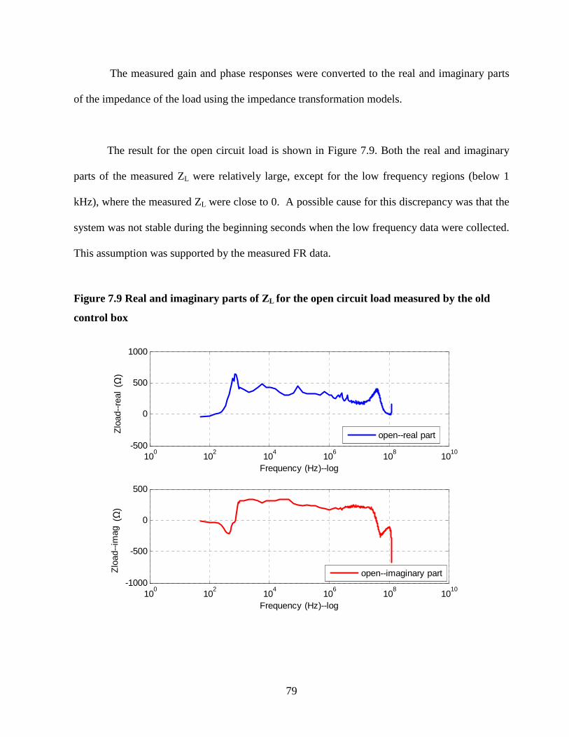
79
The measured gain and phase responses were converted to the real and imaginary parts
of the impedance of the load using the impedance transformation models.
The result for the open circuit load is shown in Figure 7.9. Both the real and imaginary
parts of the measured ZL were relatively large, except for the low frequency regions (below 1
kHz), where the measured ZL were close to 0. A possible cause for this discrepancy was that the
system was not stable during the beginning seconds when the low frequency data were collected.
This assumption was supported by the measured FR data.
Figure 7.9 Real and imaginary parts of ZL for the open circuit load measured by the old
control box
100
102
104
106
108
1010
-500
0
500
1000
Frequency (Hz)--log
Zlo
ad--
real
(oh
m)
100
102
104
106
108
1010
-1000
-500
0
500
Frequency (Hz)--log
Zlo
ad--
imag
(oh
m)
open--real part
open--imaginary part
(Ω)
(Ω)

80
Results for the short circuit and 50Ω resistor loads are shown in Figures 7.10 and 7.11,
respectively. For the short circuit load, both the real and imaginary parts of the measured ZL
were close to 0Ω at frequencies below 50 MHz. For the 50Ω resistor load, the real part was close
to 50Ω and the imaginary part was close to 0Ω at the frequencies higher than 1 kHz. For
frequencies below 1 kHz, measured imaginary part of ZL deviated from the actual values
probably due to signal instability as discussed previously.
Figure 7.10 Real and imaginary parts of ZL for the short circuit load measured by the old
control box
100
102
104
106
108
1010
-200
0
200
400
600
Frequency (Hz)--log
Zlo
ad--
real
(oh
m)
100
102
104
106
108
1010
-400
-200
0
200
400
Frequency (Hz)--log
Zlo
ad--
imag
(oh
m)
short--real part
short--imaginary part
(Ω)
(Ω)

81
Figure 7.11 Real and imaginary parts of ZL for the 50Ω resistor load measured by the old
control box
100
102
104
106
108
1010
-50
0
50
100
Frequency (Hz)--log
Zlo
ad--
real
(oh
m)
100
102
104
106
108
1010
-30
-20
-10
0
10
Frequency (Hz)--log
Zlo
ad--
imag
(oh
m)
50ohm--real part
50ohm--imaginary part
50Ω—real part
50Ω—imaginary part
(Ω)
(Ω)

82
Gain and phase responses measured by the new control box for open, short and 50Ω
loads plotted against linear and logarithm frequency axes are shown in Figures 7.12 and 7.13,
respectively. The measured gain and phase responses were obviously different among the open,
short and 50Ω resistor loads.
Figure 7.12 Gain responses measured by the new control box for open, short and 50Ω loads
on (a) linear and (b) log scales
0 0.5 1 1.5 2 2.5 3 3.5 4
x 108
-30
-20
-10
0
10
Frequency (Hz)--linear
Gai
n (d
B)
open
short
50ohm
(a)
102
104
106
108
1010
-30
-20
-10
0
10
Frequency (Hz)--log
Gai
n (d
B)
open
short
50ohm
(b)
50Ω
50Ω
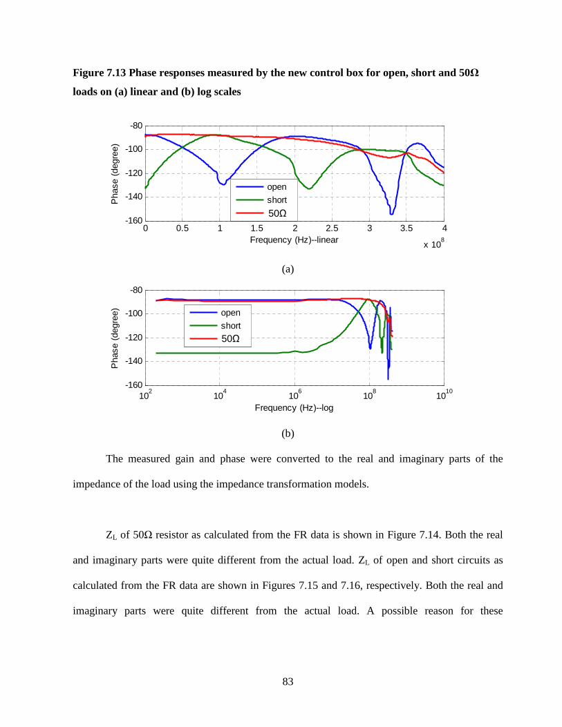
83
Figure 7.13 Phase responses measured by the new control box for open, short and 50Ω
loads on (a) linear and (b) log scales
0 0.5 1 1.5 2 2.5 3 3.5 4
x 108
-160
-140
-120
-100
-80
Frequency (Hz)--linear
Pha
se (
degr
ee)
open
short
50ohm
(a)
102
104
106
108
1010
-160
-140
-120
-100
-80
Frequency (Hz)--log
Pha
se (
degr
ee)
open
short
50ohm
(b)
The measured gain and phase were converted to the real and imaginary parts of the
impedance of the load using the impedance transformation models.
ZL of 50Ω resistor as calculated from the FR data is shown in Figure 7.14. Both the real
and imaginary parts were quite different from the actual load. ZL of open and short circuits as
calculated from the FR data are shown in Figures 7.15 and 7.16, respectively. Both the real and
imaginary parts were quite different from the actual load. A possible reason for these
50Ω
50Ω
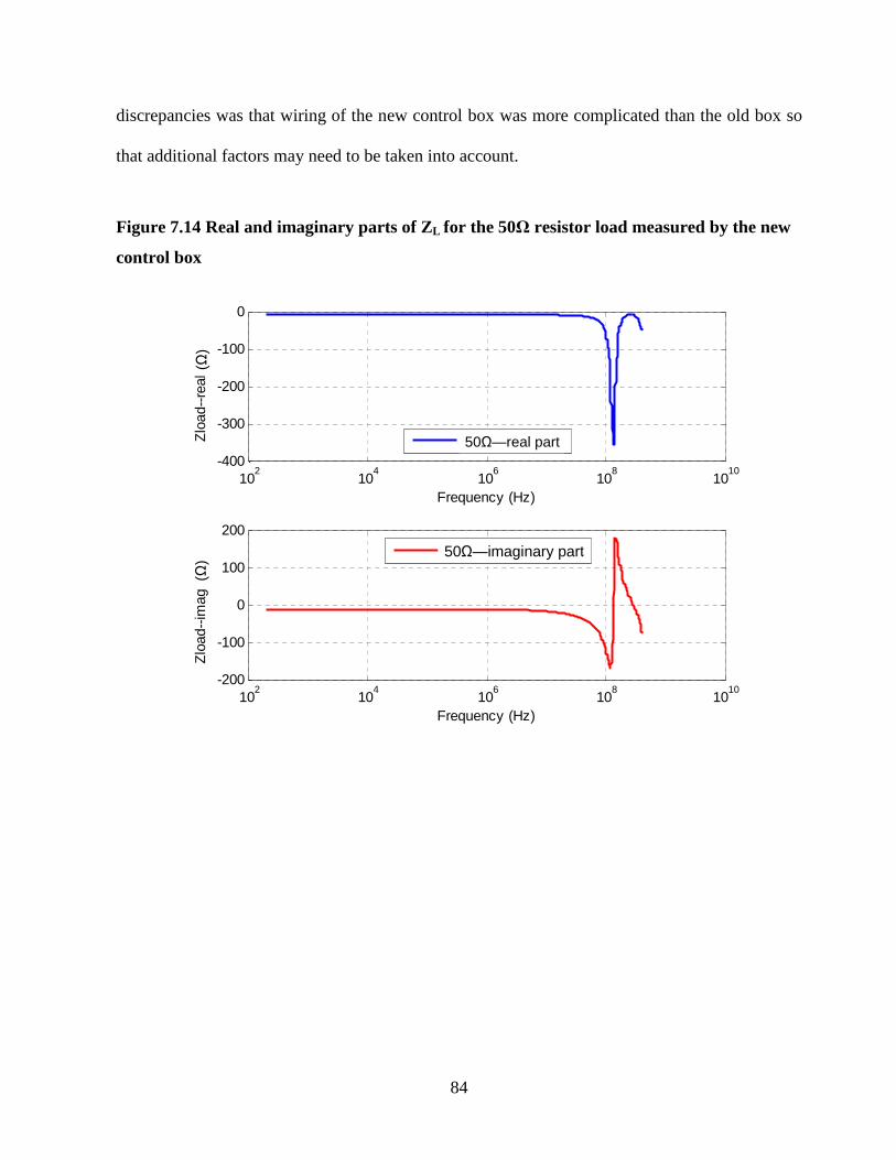
84
102
104
106
108
1010
-400
-300
-200
-100
0
Frequency (Hz)
Zlo
ad--
real
(oh
m)
102
104
106
108
1010
-200
-100
0
100
200
Frequency (Hz)
Zlo
ad--
imag
(oh
m)
50ohm--real part
50ohm--imaginary part
50Ω—real part
50Ω—imaginary part
(Ω)
(Ω)
discrepancies was that wiring of the new control box was more complicated than the old box so
that additional factors may need to be taken into account.
Figure 7.14 Real and imaginary parts of ZL for the 50Ω resistor load measured by the new
control box
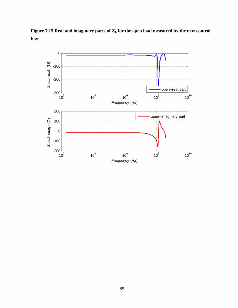
85
Figure 7.15 Real and imaginary parts of ZL for the open load measured by the new control
box
102
104
106
108
1010
-300
-200
-100
0
Frequency (Hz)
Zlo
ad--
real
(oh
m)
102
104
106
108
1010
-200
-100
0
100
200
Frequency (Hz)
Zlo
ad--
imag
(oh
m)
open--real part
open--imaginary part
(Ω)
(Ω)

86
Figure 7.16 Real and imaginary parts of ZL for the short load measured by the new control
box
102
104
106
108
1010
-300
-200
-100
0
Frequency (Hz)--log
Zlo
ad--
real
(oh
m)
short--real part
102
104
106
108
1010
-200
-100
0
100
200
Frequency (Hz)--log
Zlo
ad--
imag
(oh
m)
short--imaginary part
In summary, relatively good results were obtained for the open, short and 50Ω resistor
loads measured by the old control box. The impedance transformation models developed for the
old control box were capable of predicting the impedances of these special loads. However, the
results obtained for the new control box were not correct.
(Ω)
(Ω)
87
7.2.2 Parallel capacitor-resistor load
This section reports the results of frequency response tests with parallel R-C loads. Only
the old control box was tested for these loads.
The real and imaginary parts of the load impedance as measured by the old control box
are compared with the actual loads in Figures 7.17 and 7.18, respectively. Three different loads
were used within different frequency ranges. Below 1 kHz, the load was a parallel connection of
a 50Ω resistor and a 10uF capacitor. While the same resistor was used for the higher frequency
regions, the capacitor used for 1 kHz – 1 MHz and above 1 MHz were 0.33uF and 68pF,
respectively.
The results showed that the real part of the load impedance measured by the old control
box was close to the actual value within the frequency range of 350 Hz – 50 MHz. For
frequencies below 350 Hz, the measured values were quite different from the actual loads. As
described in Section 7.2.1, difference between measured and actual impedances at the low
frequencies was probably due to the instability of the control box during the first few seconds of
measurement. Giving a “warmup” time at the beginning of measurement may help alleviate this
problem. The result showed that the measured imaginary part of load impedances was close to
the actual load at most frequencies, except for frequencies above 50 MHz.

88
Figure 7.17 Comparison of real part of the load impedance measured by the old control
box with that calculated for the actual loads
-50
0
50
100
150
200
1.0E+00 1.0E+01 1.0E+02 1.0E+03 1.0E+04 1.0E+05 1.0E+06 1.0E+07 1.0E+08 1.0E+09
Frequency(Hz)
Rea
l par
t of i
mpe
danc
e (Ω
)
measured real part of load terminated impedance
actual real part of load impedance
paralle with 10uF capacitor
paralle with 0.33uF capacitor
paralle with 68pF capacitor
1 101 102 103 104 105 106 107 108 109
Figure 7.18 Comparison of imaginary part of the load impedance measured by the old
control box with that calculated for the actual loads
-80
-60
-40
-20
0
20
40
60
80
1.0E+00 1.0E+01 1.0E+02 1.0E+03 1.0E+04 1.0E+05 1.0E+06 1.0E+07 1.0E+08 1.0E+09
Frequency(Hz)
Imag
par
t of
impe
danc
e (Ω
)
measured imag part of load terminated impedance
actual imag part of load impedance
paralle with 10uF capacitor
paralle with 0.33uF capacitor
paralle with 68pF capacitor
1 101 102 103 104 105 106 107 108 109

89
In summary, the impedance transformation models were able to predict the impedance of
parallel R-C loads at frequencies below 50 MHz. However, the models needed to be further
improved to reduce the predicted error.
7.3 Coaxial cables of different lengths with the same load
Gain and phase responses measured by the old control box with the short (37cm) and
long (141cm) cables, both terminated with a 50Ω resistor, are shown against linear and logarithm
frequency axes in Figures 7.19 and 7.20, respectively. The results showed that both gain and
phase responses measured with the short and the long cables were very similar within the
measurement frequency range, indicating that the measurement was not affected by the cable
length. This is probably due to the fact that the characteristic impedance of both cables was 50Ω,
which matched the load impedance.
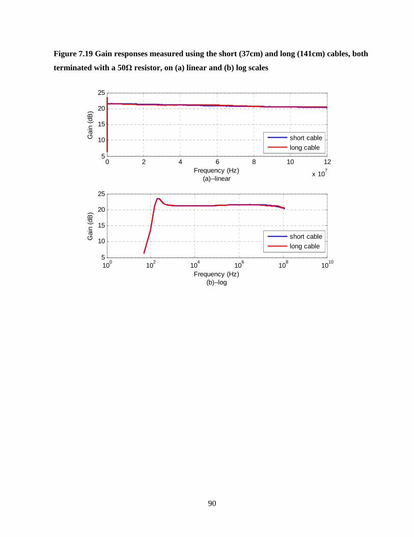
90
Figure 7.19 Gain responses measured using the short (37cm) and long (141cm) cables, both
terminated with a 50Ω resistor, on (a) linear and (b) log scales
0 2 4 6 8 10 12
x 107
5
10
15
20
25
Frequency (Hz)(a)--linear
Gai
n (d
B)
100
102
104
106
108
1010
5
10
15
20
25
Frequency (Hz)(b)--log
Gai
n (d
B)
short cable
long cable
short cable
long cable

91
Figure 7.20 Phase responses measured using the short (37cm) and long (141cm) cables,
both terminated with a 50Ω resistor, on (a) linear and (b) log scales
0 2 4 6 8 10 12
x 107
-50
0
50
100
Frequency (Hz)(a)--linear
Pha
se (
degr
ee)
100
102
104
106
108
1010
-50
0
50
100
Frequency (Hz)(b)--log
Pha
se (
degr
ee)
short cable
long cable
short cable
long cable
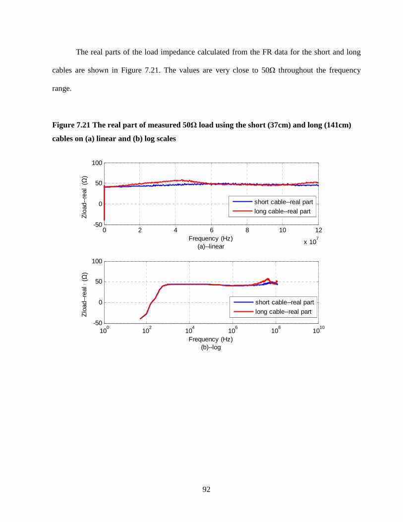
92
The real parts of the load impedance calculated from the FR data for the short and long
cables are shown in Figure 7.21. The values are very close to 50Ω throughout the frequency
range.
Figure 7.21 The real part of measured 50Ω load using the short (37cm) and long (141cm)
cables on (a) linear and (b) log scales
0 2 4 6 8 10 12
x 107
-50
0
50
100
Frequency (Hz)(a)--linear
Zlo
ad--
real
(oh
m)
100
102
104
106
108
1010
-50
0
50
100
Frequency (Hz)(b)--log
Zlo
ad--
real
(oh
m)
short cable--real part
long cable--real part
short cable--real part
long cable--real part
(Ω)
(Ω)
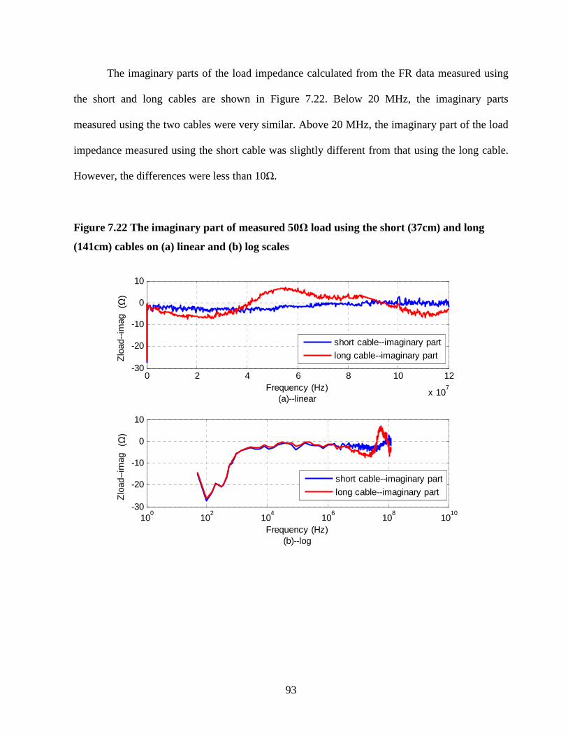
93
The imaginary parts of the load impedance calculated from the FR data measured using
the short and long cables are shown in Figure 7.22. Below 20 MHz, the imaginary parts
measured using the two cables were very similar. Above 20 MHz, the imaginary part of the load
impedance measured using the short cable was slightly different from that using the long cable.
However, the differences were less than 10Ω.
Figure 7.22 The imaginary part of measured 50Ω load using the short (37cm) and long
(141cm) cables on (a) linear and (b) log scales
0 2 4 6 8 10 12
x 107
-30
-20
-10
0
10
Frequency (Hz)(a)--linear
Zlo
ad--
imag
(oh
m)
100
102
104
106
108
1010
-30
-20
-10
0
10
Frequency (Hz)(b)--log
Zlo
ad--
imag
(oh
m)
short cable--imaginary part
long cable--imaginary part
short cable--imaginary part
long cable--imaginary part
(Ω)
(Ω)
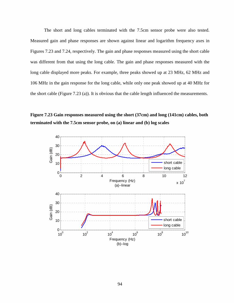
94
The short and long cables terminated with the 7.5cm sensor probe were also tested.
Measured gain and phase responses are shown against linear and logarithm frequency axes in
Figures 7.23 and 7.24, respectively. The gain and phase responses measured using the short cable
was different from that using the long cable. The gain and phase responses measured with the
long cable displayed more peaks. For example, three peaks showed up at 23 MHz, 62 MHz and
106 MHz in the gain response for the long cable, while only one peak showed up at 40 MHz for
the short cable (Figure 7.23 (a)). It is obvious that the cable length influenced the measurements.
Figure 7.23 Gain responses measured using the short (37cm) and long (141cm) cables, both
terminated with the 7.5cm sensor probe, on (a) linear and (b) log scales
0 2 4 6 8 10 12
x 107
0
10
20
30
40
Frequency (Hz)(a)--linear
Gai
n (d
B)
100
102
104
106
108
1010
0
10
20
30
40
Frequency (Hz)(b)--log
Gai
n (d
B)
short cable
long cable
short cable
long cable
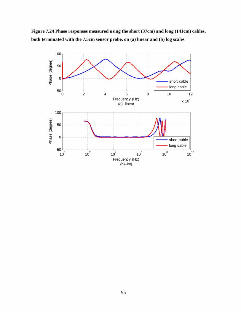
95
Figure 7.24 Phase responses measured using the short (37cm) and long (141cm) cables,
both terminated with the 7.5cm sensor probe, on (a) linear and (b) log scales
0 2 4 6 8 10 12
x 107
-50
0
50
100
Frequency (Hz)(a)--linear
Pha
se (
degr
ee)
100
102
104
106
108
1010
-50
0
50
100
Frequency (Hz)(b)--log
Pha
se (
degr
ee)
short cable
long cable
short cable
long cable
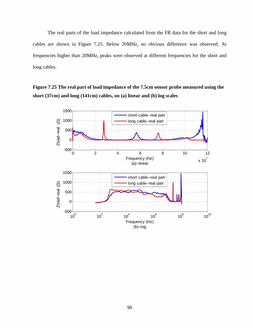
96
The real parts of the load impedance calculated from the FR data for the short and long
cables are shown in Figure 7.25. Below 20MHz, no obvious difference was observed. At
frequencies higher than 20MHz, peaks were observed at different frequencies for the short and
long cables.
Figure 7.25 The real part of load impedance of the 7.5cm sensor probe measured using the
short (37cm) and long (141cm) cables, on (a) linear and (b) log scales
0 2 4 6 8 10 12
x 107
-500
0
500
1000
1500
Frequency (Hz)(a)--linear
Zlo
ad--
real
(oh
m)
short cable--real part
long cable--real part
100
102
104
106
108
1010
-500
0
500
1000
1500
Frequency (Hz)(b)--log
Zlo
ad--
real
(oh
m)
short cable--real part
long cable--real part
(Ω)
(Ω)
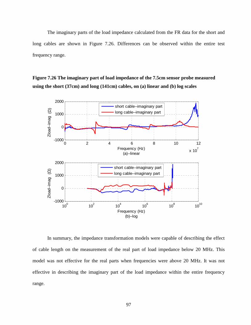
97
The imaginary parts of the load impedance calculated from the FR data for the short and
long cables are shown in Figure 7.26. Differences can be observed within the entire test
frequency range.
Figure 7.26 The imaginary part of load impedance of the 7.5cm sensor probe measured
using the short (37cm) and long (141cm) cables, on (a) linear and (b) log scales
0 2 4 6 8 10 12
x 107
-1000
0
1000
2000
Frequency (Hz)(a)--linear
Zlo
ad--
imag
(oh
m)
short cable--imaginary part
long cable--imaginary part
100
102
104
106
108
1010
-1000
0
1000
2000
Frequency (Hz)(b)--log
Zlo
ad--
imag
(oh
m)
short cable--imaginary part
long cable--imaginary part
In summary, the impedance transformation models were capable of describing the effect
of cable length on the measurement of the real part of load impedance below 20 MHz. This
model was not effective for the real parts when frequencies were above 20 MHz. It was not
effective in describing the imaginary part of the load impedance within the entire frequency
range.
(Ω)
(Ω)

98
7.4 Problem with the gain and phase detector
During the experiment, the measured phase angles all fell in the 0°~90° range. A general
trend was to bounce between 0° and 90° as frequency increased. This trend did not agree with
the model. To investigate this discrepancy, a series of tests were conducted on gain and phase
detector. Results of these tests are discussed in this section.
7.4.1 Test on a gain and phase detector evaluation board
An evaluation board for the 8302 gain and phase detector (Analog Devices, Inc.) was
used in the test. A signal generator (Agilent 33220A) was used to generate sine wave signal,
which was sent to channel B (INPB) of the gain and phase detector. An RC circuit formed a low-
pass filter with a corner frequency of 1 MHz. This filter generated a delayed sine wave, which
was sent to channel A (INPA) of the gain and phase detector (Figure 7.27). Thus, the phase delay
generated by the RC circuit was measured by the gain and phase detector. Twelve frequencies,
including 500 Hz, 1, 10,100 and 500 kHz, and 1, 2, 5, 8, 10, 15, and 20 MHz, were selected for
the test. Test at each frequency was repeated twice.
Figure 7.27 An RC circuit generated phase delays
GND
INPB INPA
GND
INPB INPAR
C
INPB
INPA
G/P
16Ω
0.01uF
GND
INPB INPA
GND
INPB INPAR
C
INPB
INPA
G/P
GND
INPB INPA
GND
INPB INPA
GND
INPB INPA
GND
INPB INPA
GND
INPB INPA
GND
INPB INPA
GND
INPB INPA
GND
INPB INPAR
C
INPB
INPA
G/PR
C
INPB
INPA
G/P
16Ω
0.01uF
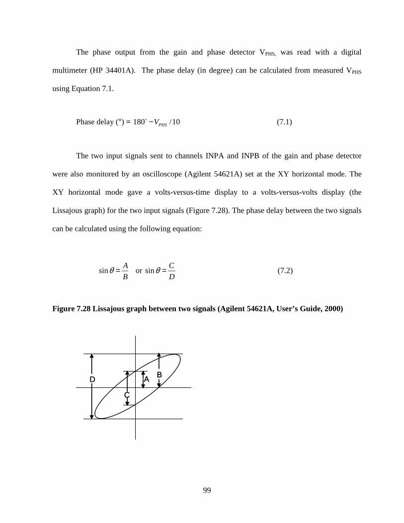
99
The phase output from the gain and phase detector VPHS, was read with a digital
multimeter (HP 34401A). The phase delay (in degree) can be calculated from measured VPHS
using Equation 7.1.
Phase delay (°) = 180 /10PHSV− (7.1)
The two input signals sent to channels INPA and INPB of the gain and phase detector
were also monitored by an oscilloscope (Agilent 54621A) set at the XY horizontal mode. The
XY horizontal mode gave a volts-versus-time display to a volts-versus-volts display (the
Lissajous graph) for the two input signals (Figure 7.28). The phase delay between the two signals
can be calculated using the following equation:
sinA
Bθ = or sin
C
Dθ = (7.2)
Figure 7.28 Lissajous graph between two signals (Agilent 54621A, User’s Guide, 2000)
DB
C
ADB
C
A

100
The phase delay observed from the oscilloscope using the Lissajous method was
compared with that measured by the gain and phase detector. The results are shown in Figures
7.29 and 7.30 on logarithmic and linear frequency axes, respectively.
Figure 7.29 Phase delay observed from the oscilloscope and measured by the gain and
phase detector on a logarithmic frequency axis
-250
-200
-150
-100
-50
0
1.0E+00 1.0E+01 1.0E+02 1.0E+03 1.0E+04 1.0E+05 1.0E+06 1.0E+07 1.0E+08
Frequency(Hz)
Pha
se d
elay
(°)
phase delay observed from Lissajous plot
phase delay measured by gain and phase detector
phase delay measured by gain and phase detector and manually adjusted to remove 180° jump

101
Figure 7.30 Phase delay observed from the oscilloscope and measured by the gain and
phase detector on a linear frequency axis
-250
-200
-150
-100
-50
0
0 5000000 10000000 15000000 20000000 25000000
Frequency(Hz)
Pha
se d
elay
(°)
phase delay observed from Lissajous plot
phase delay measured by gain and phase detector
phase delay measured by gain and phase detector and manually adjusted to remove 180° jump
The results showed that the phase delay observed from Lissajous method had the same
trend with that measured by the gain and phase detector as the frequencies increased, although
larger discrepancies took place at the frequencies higher than 5 MHz. The errors may have
resulted from inaccuracy in data reading on Lissajous plot. At 20 MHz, the phase delay angle
observed from Lissajous plot was -213°. However, the gain and phase detector gave -41° at this
frequency. This was because that the range of the phase reading from the gain and phase detector
was from -180° to 0° (or 0°~180°). Due to the periodicity of the arctangent function, -41° was
adjusted to -221° to remove the 180° jump and to maintain the continuity of measured phase
delay.

102
7.4.2 Test on the old control box at single frequencies
In this part of the experiment, signals on the channels A (INPA) and B (INPB) of the gain
and phase detector in the old control box were monitored and recorded by an oscilloscope
(Agilent 54621A). The 7.5cm probe was connected to the old control box through the short
(37cm) coaxial cable. The probe was placed in air. The system ran at frequencies between 20
MHz and 110 MHz with 10 MHz interval. From Figure 7.24 (Section 7.3), the phase responses
measured with the long cable displayed several peaks and valleys at various frequencies. In order
to study this trend, frequencies selected were those close to the turning points of the phase
response measured with the long cable.
Signals on the INPB and INPA inputs at 50, 60, 70 and 80 MHz recorded by the
oscilloscope are shown in Figure 7.31. The results showed that the phase delay between INPA
and INPB continuously increased with frequency with no peaks and valleys observed.
Obviously, this result was different from the phase response data measured using the old control
box.
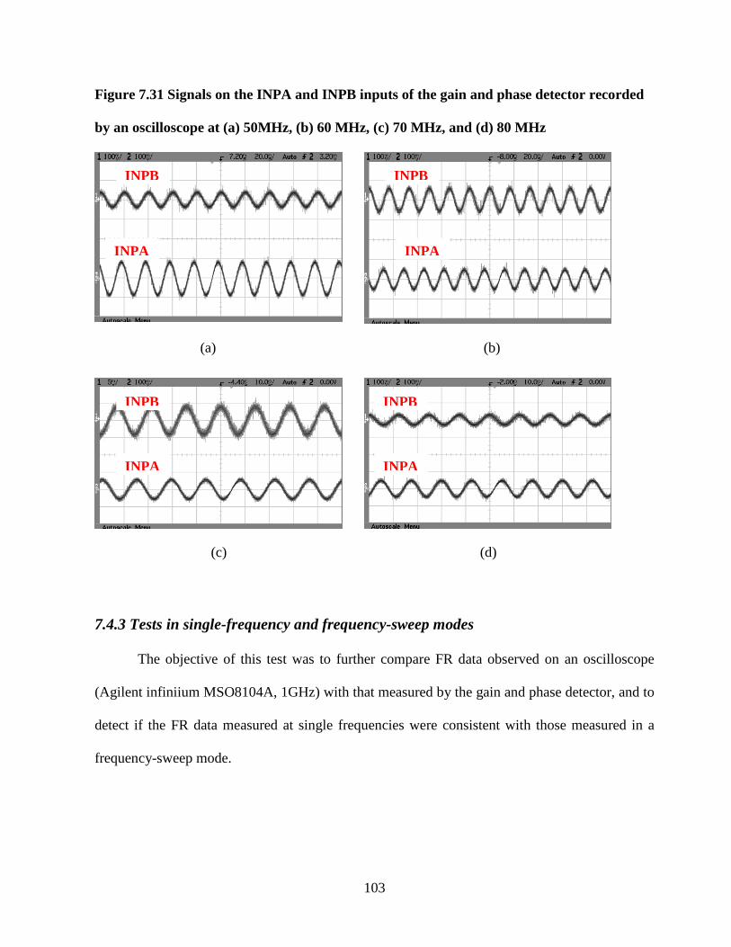
103
Figure 7.31 Signals on the INPA and INPB inputs of the gain and phase detector recorded
by an oscilloscope at (a) 50MHz, (b) 60 MHz, (c) 70 MHz, and (d) 80 MHz
1
7.4.3 Tests in single-frequency and frequency-sweep modes
The objective of this test was to further compare FR data observed on an oscilloscope
(Agilent infiniium MSO8104A, 1GHz) with that measured by the gain and phase detector, and to
detect if the FR data measured at single frequencies were consistent with those measured in a
frequency-sweep mode.
(a) (b)
(c) (d)
INPA INPA
INPA
INPB
INPB INPB
INPA
INPB

104
7.4.3.1 Comparison of measurements by the control box and oscilloscope at the single
frequency mode
For the single frequency test, signal at each selected frequency was run for 3.5min so that
the oscilloscope (Agilent infiniium MSO8104A, 1GHz) had sufficient time to record the signals
at INPA and INPB. Frequencies selected were those at or around the turning points of the phase
response measured with the long cable, including 40, 44.8, 50, 55, 62, 70, 75, 82.6, 87, 90, 95,
100, 104.8, and 110MHz (Figure 7.24). The measurement at each frequency was repeated 10
times. Both the short and long cables were used in this test.
Results of these tests are shown in Figures 7.32 – 7.35. For the short cable, the measured
gain response had a similar trend with that observed on the oscilloscope. However, the gain
measured by the control box was in general higher than that observed on the oscilloscope by
about 10dB (Figure 7.32). Similar trend can be found for the data obtained via the long cable at
frequency higher than 70 MHz (Figure 7.33). The phase responses measured by the control box
and the oscilloscope were almost identical below 60 MHz and started to deviate from each other
when the phase angle reached 90° (Figure 7.34 and 7.35). An effort to correct the phase angle
based on the periodicity of the arctangent function also failed to yield a reasonable result.

105
Figure 7.32 Comparison of gain measured by the old control box with that observed on the
oscilloscope. The short cable was used in the test.
0
5
10
15
20
25
30
35
3E+07 4E+07 5E+07 6E+07 7E+07 8E+07 9E+07 1E+08 1.1E+08 1.2E+08
Frequency(Hz)
Gai
n (d
B)
measured by control system
observed by infiniium oscilloscope
Figure 7.33 Comparison of gain measured by the old control box with that observed on the
oscilloscope. The long cable was used in the test.
0
5
10
15
20
25
30
3E+07 4E+07 5E+07 6E+07 7E+07 8E+07 9E+07 1E+08 1.1E+08 1.2E+08
Frequency(Hz)
Gai
n (d
B)
measured by control system
observed by infiniium oscilloscope

106
Figure 7.34 Comparison of phase measured by the old control box with that observed on
the oscilloscope. The short cable was used in the test.
-100
0
100
200
300
400
500
600
3E+07 4E+07 5E+07 6E+07 7E+07 8E+07 9E+07 1E+08 1.1E+08 1.2E+08
Frequency(Hz)
Pha
se (d
egre
e)
measured by control system
observed by infiniium oscilloscope
Figure 7.35 Comparison of phase measured by the old control box with that observed on
the oscilloscope. The long cable was used in the test.
0
100
200
300
400
500
600
3E+07 4E+07 5E+07 6E+07 7E+07 8E+07 9E+07 1E+08 1.1E+08 1.2E+08
Frequency(Hz)
Pha
se (
degr
ee)
measured by control system
observed by infiniium oscilloscope
107
7.4.3.2 Comparison between single-frequency and frequency-sweep modes
Comparisons of gain and phase measured at single frequencies with that measured in a
frequency-sweep mode for the short and long cables are shown in Figures 7.36 – 7.39.
For the short cable, the gain responses measured at single frequencies were different from
that measured in the frequency-sweep mode. The frequency-sweep mode gave smoother gain
responses than the single frequency mode (Figure 7.36). A relatively similar trend can be found
for the data obtained via the long cable (Figure 7.37). The phase responses measured at single
frequencies were quite different from that measured in the frequency-sweep mode for the short
cable (Figure 7.38). However, for the long cable, a similar trend can be observed for the phase
responses within the frequency range from 44.8 MHz to 75 MHz and 95 MHz to 110 MHz
(Figure 7.39).

108
Figure 7.36 Comparison of gain measured at the single frequency and the frequency sweep
modes. The short cable was used in the test.
0
5
10
15
20
25
30
35
3.0E+07 4.0E+07 5.0E+07 6.0E+07 7.0E+07 8.0E+07 9.0E+07 1.0E+08 1.1E+08 1.2E+08
Frequency(Hz)
Gai
n (d
B)
Gain by single freq test
Gain by sweep freq test
Figure 7.37 Comparison of gain measured at the single frequency and the frequency sweep
modes. The long cable was used in the test.
0
5
10
15
20
25
30
35
3.0E+07 4.0E+07 5.0E+07 6.0E+07 7.0E+07 8.0E+07 9.0E+07 1.0E+08 1.1E+08 1.2E+08
Frequency(Hz)
Gai
n (d
B)
Gain by single freq test
Gain by sweep freq test

109
Figure 7.38 Comparison of phase measured at the single frequency and the frequency
sweep modes. The short cable was used in the test.
-10
0
10
20
30
40
50
60
70
80
90
3.0E+07 4.0E+07 5.0E+07 6.0E+07 7.0E+07 8.0E+07 9.0E+07 1.0E+08 1.1E+08 1.2E+08
Frequency(Hz)
Pha
se (
degr
ee)
Phase angle by single freq test
Phase angle by sweep freq test
Figure 7.39 Comparison of phase measured at the single frequency and the frequency
sweep modes. The long cable was used in the test.
-10
0
10
20
30
40
50
60
70
80
90
3.0E+07 4.0E+07 5.0E+07 6.0E+07 7.0E+07 8.0E+07 9.0E+07 1.0E+08 1.1E+08 1.2E+08
Frequency(Hz)
Pha
se (
degr
ee)
Phase angle by single freq test
Phase angle by sweep freq test

110
In summary, the issues with the gain and phase detector were not solved through this
experiment. One of the possible reasons for the discrepancy in gain and phase measurement is
that the signal from the sensor probe (INPB input) was noisy. The discrepancy between signals
measured at the single frequency and frequency-sweep modes may indicate that, for frequency
sweeping, a longer waiting time is needed between frequency changes. More tests are needed to
solve these issues.
111
CHAPTER 8 - Conclusions
Conclusions drawn from each stage of this study are summarized as follows:
8.1 Control system
A real-time control system for a frequency response (FR)-based permittivity sensor was
developed. A C program was developed in the TASKING Embedded Development Environment
to control the system. The new control system embodied improvements over a previously
designed system in the following aspects:
The system used a printed circuit board.
The measurement frequency range was extended from 120 MHz to 400 MHz.
The resolution of measured FR data was improved by using programmable gain
amplifiers.
A data storage module was added to the system.
A temperature measurement module was added to the system.
An LCD display and a keypad were added to the system to display the frequency
response data with corresponding frequencies and to allow users to enter commands.
8.2 Impedance transformation models tests
Impedance transformation models for the control system with (1) sensor probes of
different sizes, (2) coaxial cables of the same length terminated with different loads, and (3)
coaxial cables of different lengths terminated with the same load were developed and tested.

112
Several additional tests for the gain and phase detector were also conducted to evaluate its
performance.
Tests on 7.5cm and 5cm probes indicated that a simple parallel R-C model did not
describe the probe impedance accurately.
Tests on the old control box and a coaxial cable terminated with three “standard”
loads - an open circuit, a short circuit, and a 50Ω resistor - indicated that the
impedance transformation models were capable of predicting the impedances of these
loads. However, the results obtained for the new control box were not satisfactory.
Test results also showed that the impedance of parallel R-C loads at frequencies
below 50 MHz can be predicted by the impedance transformation models. However,
the models needed to be further improved to reduce the prediction error.
Tests on coaxial cables with different lengths indicated that the impedance
transformation model were capable of describing the effect of cable length on the
measurement of the real part of load impedance only at frequencies below 20 MHz.
The model was not effective in describing the imaginary part of the load impedance
within the entire frequency range tested.
Issues with the gain and phase detector need additional study.

113
CHAPTER 9 - Recommended Future Research
The following technical issues need to be further investigated:
1. Signals from the thermocouple were not stable within the frequency range tested. A
greater signal drop can be observed at frequencies between 20 and 110MHz. Causes for signal
drop need to be further investigated.
2. Software for saving FR data to the newly added flash memory needs to be completed.
3. Tests on sensor probes of different sizes have indicated that the impedance model for
sensor probe was not accurate. An improved model that incorporates impedances of the
connecting wires and bolts needs to be studied. Moreover, a new, simple sensor probe with only
two parallel plates is recommended. This probe can be used to test “standard” dielectric liquids
with known permittivities and compare permittivities derived from the FR data with the known
values.
4. Issues with the gain and phase detector need additional study. The following procedure
is recommended to identify the factors that limited the measured phase difference to 0-90º. 1)
Repeat the test described in Section 7.4.1 with the signal generator (Figure 7.27) replaced with
an AD9854 evaluation board. Results of this test can be used to explain whether the issue is
related to the AD9854 evaluation board. 2) If phase differences of above 90º can still be

114
measured, replace the RC circuit in Figure 7.27 with Rref (Figures 4.1, 4.3, 5.5, and 5.6) and a
sensor probe with a coaxial cable, and then observe the measured phase difference range.
5. Discrepancies in gain and phase responses measured at the single-frequency and the
frequency-sweep modes need to be further studied through tests. A longer waiting time may be
added during frequency switching.

115
References
Abdulnour, J., C. Akyel and K. Wu. 1995. A generic approach for permittivity measurement of
dielectric materials using a discontinuity in a rectangular waveguide or a microstrip line. IEEE
Transactions on Microwave Theory and Techniques 43(5): 1060-1066.
Agilent Technologies. 2000. Agilent 54621A oscilloscope user's guide.
Analog Devices, Inc. 1999. AD623 data sheet. Available online at http://www.analog.com.
Analog Devices, Inc. 2002. AD8302 data sheet. Available online at http://www.analog.com.
Analog Devices, Inc. 2003a. AD9858 data sheet. Available online at http://www.analog.com.
Analog Devices, Inc. 2003b. AD9833 data sheet. Available online at http://www.analog.com.
Analog Devices, Inc. 2003c. AD8186 data sheet. Available online at http://www.analog.com.
Afsar, M.N., J.R. Birch, R.N. Clarke and G.W. Chantry. 1986. The measurement of the
properties of materials. Proceedings of the IEEE 74(1): 183-199.
Baker-Jarvis, J., E.J. Vanzura and W.A. Kissick. 1990. Improved technique for determining
complex permittivity with the transmission/reflection method. IEEE Transactions on Microwave
Theory and Techniques 38(8): 1096-1103.
Bois, K.J., L.F. Handjojo, A.D. Benally, K. Mubarak and R. Zoughi. 1999. Dielectric plug-
loaded two-port transmission line measurement technique for dielectric property characterization

116
of granular and liquid materials. IEEE Transactions on Instrumentation and Measurement 48(6):
1141-1148.
Bussey, H.E. 1967. Measurement of RF properties of materials a survey. Proceedings of the
IEEE 55(6): 1046-1053.
Catala-Civera, J.M., A.J. Canos, F.L. Penaranda-Foix and de los Reyes Davo, E. 2003. Accurate
determination of the complex permittivity of materials with transmission reflection
measurements in partially filled rectangular waveguides. IEEE Transactions on Microwave
Theory and Techniques 51(1 Part 1): 16-24.
Chen, L., C.K. Ong, C.P. Neo, V.V. Varadan and V.K. Varadan. 2004. Microwave electronics:
measurement and material characterization. Wiley Hoboken, NJ.
Coleman, C., 2004. An Introduction to Radio Frequency Engineering. The press syndicate of the
University of Cambridge.
Crystek Crystals Corporation. 2005. CVCSO-914-1000 crystal oscillator data sheet. Available
online at http:www.crystek.com.
Dean, T.J., J.P. Bell and A.J.B. Baty. 1987. Soil moisture measurement by an improved
capacitance technique. I: Sensor design and performance. Journal of hydrology (Amsterdam)
93(1-2): 67-78.
Dionigi, M., A. Ocera, E. Fratticcioli and R. Sorrentino. 2004. A new resonant probe for
dielectric permittivity measurement. Microwave Conference, 2004. 34th European 2: 673-676.

117
Dudorov, S.N., D.V. Lioubtchenko, J.A. Mallat and A.V. Raisanen. 2005. Millimeter-wave
permittivity measurement of deposited dielectric films using the spherical open resonator. IEEE
Microwave and Wireless Components Letters [see also IEEE Microwave and Guided Wave
Letters] 15(9): 564-566.
Fan, G., 2002. Simultaneous sensing of soil conductive and capacitive properties. A Master’s
thesis, Department of Biological and Agricultural Engineering, Kansas State University.
Fratticcioli, E., M. Dionigi and R. Sorrentino. 2004. A simple and low-cost measurement system
for the complex permittivity characterization of materials. IEEE Transactions on Instrumentation
and Measurement 53(4): 1071-1077.
Ghodgaonkar, D.K., V.V. Varadan and V.K. Varadan. 1990. Free-space measurement of
complex permittivity and complex permeability of magnetic materials at microwave frequencies.
IEEE Transactions on Instrumentation and Measurement 39(2): 387-394.
Infineon technologies. 2001. C167CR data sheet. Available online at http://www.infineon.com.
Lee, K.H., 2005. A dielectric permittivity sensor for simultaneous measurement of multiple soil
properties. A Ph.D. Dissertation, Department of Biological and Agricultural Engineering, Kansas
State University.
Lee, K.H., N. Zhang, W.B. Kuhn, and G.J. Kluitenberg. 2007a. A frequency-response
permittivity sensor for simultaneous measurement of multiple soil properties: Part I. The
frequency-response method. Transactions of the ASABE, 50(6): 2315-2326.
118
Lee, K.H. and N. Zhang. 2007b. A frequency-response permittivity sensor for simultaneous
measurement of multiple soil properties: Part II. Calibration-model tests. Transactions of the
ASABE, 50(6): 2327-2336.
Matytsin, S.M., K.N. Rozanov and N.A. Simonov. 1996. Permittivity measurement using slotted
coaxial resonator. IEEE Instrumentation and Measurement Technology Conference, 1996.
IMTC-96. Conference Proceedings. 'Quality Measurements: The Indispensable Bridge between
Theory and Reality' 2:(987-990).
Meitzler, A.H. and G.S. Saloka. 1992. Two alternative, dielectric-effect, flexible-fuel sensors.
SAE transactions 101(3): 1455-1466.
Microchip Technology Inc.. 2003. MCP6S21 data sheet. Available online at
http://www.microchip.com.
Microchip Technology Inc.. 2006. 25AA1024 data sheet. Available online at
http://www.microchip.com.
Micro/sys. Inc. 2001. LC0240 & KEYPAD16 user's manual.
National Semiconductor, 2008. LM185-2.5 data sheet. Available online at
http://www.national.com.
Nelson, S.O. 1999. Dielectric Properties Measurement Techniques and Applications.
Transactions of the ASAE-American Society of Agricultural Engineers 42 (2):523-530.
119
Nelson, S.O. 1991. Dielectric properties of agricultural products: measurements and applications.
IEEE transactions on electrical insulation 26(5): 845-869.
Nelson, S.O. 2003. Frequency-and temperature-dependent permittivities of fresh fruits and
vegetables from 0.01 to 1.8 GHz. Transactions of the ASAE-American Society of Agricultural
Engineers 46(2): 567-576.
Nelson, S.O., W.R. Forbus Jr and K.C. Lawrence. 1995. Assessment of microwave permittivity
for sensing peach maturity. Transactions of the ASAE-American Society of Agricultural
Engineers 38(2): 579-585.
Nozaki, R. and T.K. Bose. 1990. Broadband complex permittivity measurements by time-domain
spectroscopy. IEEE Transactions on Instrumentation and Measurement 39(6): 945-951.
Nyfors, E. 2000. Industrial Microwave Sensors—A Review. Subsurface Sensing Technologies
and Applications 1(1): 23-43.
Ocera, A., M. Dionigi, E. Fratticcioli and R. Sorrentino. 2006. A novel technique for complex
permittivity measurement based on a planar four-port device. IEEE Transactions on Microwave
Theory and Techniques 54(6): 2568.
Payero, J.O., D.D. Tarkalson and S. Irmak. 2006. Use of time domain reflectometry for
continuous monitoring of nitrate-nitrogen in soil and water. Applied Engineering in Agriculture
22(5): 689-700.
PHYTEC America, LLC. 1999. kitCON-167 Hardware-Manual. Available online at
http://www.phytec.com
120
Raveendranath, U., J. Jacob and K.T. Mathew. 1996. Complex permittivity measurement of
liquids with coaxial cavity resonators using a perturbation technique. Electronics Letters 32(11):
988-990.
Robinson, D.A., C.M.K. Gardner and J.D. Cooper. 1999. Measurement of relative permittivity in
sandy soils using TDR, capacitance and theta probes: comparison, including the effects of bulk
soil electrical conductivity. J HYDROL 223(3): 198-211.
Robinson, D.A., S.B. Jones, J.M. Wraith, D.Or and S.P. Friedman. 2003. A Review of Advances
in Dielectric and Electrical Conductivity Measurement in Soils Using Time Domain
Reflectometry. Vadose Zone Journal 2(4): 444-475.
Sheen, N.I. and I.M. Woodhead. 1999. An open-ended coaxial probe for broad-band permittivity
measurement of agricultural products. Journal of Agricultural Engineering Research 74(2): 193-
202.
Sri Ranjan, R. and C.J. Domytrak. 1997. Effective volume measured by TDR miniprobes.
Transactions of the ASAE-American Society of Agricultural Engineers 40(4): 1059-1066.
STMicroelectronics. 1999. TS925 data sheet. Available online at http://www.st.com.
Stoakes, D.S. and K.D. Brock. 1973. Oil Permittivity sensor. United States Patent.
Stuchly, S.S., M.A. Rzepecka and M.F. Iskander. 1974. Permittivity measurements at microwave
frequencies using lumped elements. IEEE Transactions on Instrumentation and Measurement
23(1): 56-62.

121
Tanaka, F., K. Morita, P. Mallikarjunan, Y.C. Hung and G.O.I. Ezeike. 2002. Analysis of
dielectric properties of rice vinegar and sake. Transactions of the ASAE-American Society of
Agricultural Engineers 45(3): 733-740.
Topp, G.C. and J.L. Davis. 1985. Measurement of Soil Water Content using Time-domain
Reflectrometry (TDR): A Field Evaluation. Soil Science Society of America Journal 49(1): 19.
Topp, G.C., S. Zegelin and I. White. 2000. Impacts of the Real and Imaginary Components of
Relative Permittivity on Time Domain Reflectometry Measurements in Soils. Soil Science
Society of America Journal 64(4): 1244-1252.
Trabelsi, S. and S.O. Nelson. 2003. Free-space measurement of dielectric properties of cereal
grain and oilseed at microwave frequencies. Measurement Science and Technology 14(5): 589-
600.
Venkatesh, M.S. and G.S.V. Raghavan. 2005. An overview of dielectric properties measuring
techniques. vol 47:7.15-7.30.
Wang, N. 2002. Design of a real-time, embedded weed-detection and spray-control system. A
Ph.D. Dissertation, Department of Biological and Agricultural Engineering, Kansas State
University.
Yu, K.B., S.G. Ogourtsov, V.G. Belenky, A.B. Maslenikov and A.S. Omar. 2000. Accurate
microwave resonant method for complex permittivity measurements of liquids [biological].
IEEE Transactions on Microwave Theory and Techniques 48(11): 2159-2164.

122
Zhang, N., G. Fan, K.H. Lee, G. Kluitenburg, and T. Loughin. 2004. Simultaneous measurement
of soil water content and salinity using a frequency-response method. Soil Science Society of
America Journal, 68:1515-1525.
Zhang, N., G. Kluitenburg, and P. Barnes. 2006. A real-time permittivity sensor for simultaneous
measurement of multiple water-quality parameters. Proceedings of Water and the Future of
Kansas Conference, March, 2006, Topeka, KS.
Zhang, N., K. Lee, X. Xi, and N. Tang. 2007. A frequency-response permittivity sensor for
simultaneous measurement of multiple properties of solid, liquid, and gaseous dielectric
materials. Proceedings of the Biological Sensorics Conference; June 15-17, 2007, Minneapolis,
MN.

123
Appendix A - Circuit schematic of the Control System
Figure A.1 Circuit schematic of the control board in the new control box
1 2 3 4 5 6
654321
D
C
B
A
Title
Number RevisionSize
B
Date: 18-Apr-2009 Sheet of File: C:\ningtang\master degree\Protel\Third.ddbDrawn By:
11
22
33
1616
44
55
66
77
88
99
1010
1111
1212
1313
1414
1515
U6Resistance
11
22
33
1616
44
55
66
77
88
99
1010
1111
1212
1313
1414
1515
U7Resistance
11
22
33
1616
44
55
66
77
88
99
1010
1111
1212
1313
1414
1515
U8Resistance
COMM1
INPA2
OFSA3
VPOS4
PFLT8
COMM7 INPB6 OFSB5
VPHS 9PSET10VREF 11
MSET 12VMAG 13MFLT 14
U5
AD8302
D0
D1
GND
D2
GND
D3
D4
R150
D5
R250
D6
D7
A0
GND
A1
A2
A3
A4
GND
A5
WR
BR
DB
SP
MO
DE
PS
0
RE
SE
T
VCC1
VCC2
VCC3
VCC4
D05
D26
D47
D68
D19
D310
D511
D712
D813
D1014
D1215
D1416
D917
D1118
D1319
D1520
A021
A222
A423
A624
A125
A326
A527
A728
A829
A1030
A1231
A1432
A933
A1134
A1335
A1536
A1637
A1838
A2039
A2240
A1741
A1942
A2143
A2344
/RD-U45
46
47
48
49
50
51
52
P6.053
P6.254
P6.455
P6.656
P6.157
P6.358
/HLD-U59
P6.760
61
62
63
64
65
66
67
68
P5.0 69
P5.2 70
P5.4 71
P5.6 72
P5.1 73
P5.3 74
P5.5 75
P5.7 76
P5.8 77P5.10 78P5.12 79P5.14 80
P5.9 81P5.11 82P5.13 83P5.15 84P2.0 85P2.2
86P2.4 87P2.6 88P2.1 89
P2.3 90P2.5 91P2.7 92P2.8 93
P2.10 94P2.12 95P2.14 96P2.9 97P2.11 98
P2.13 99P2.15 100P3.0 101P3.2 102P3.4 103P3.6
104P3.1 105P3.3 106P3.5 107
P3.7 108P3.8 109P3.10 110/WRH
111/RDY-U 112P3.9 113P3.11 114P3.13 115P3.15 116
P7.0 117P7.2 118P7.4 119P7.6
120P7.1 121P7.3 122P7.5 123P7.7 124P8.0 125
P8.2 126P8.4 127P8.6 128P8.1
129P8.3 130P8.5 131P8.7 132
133 134 135 136 137
138 139 140 141
142 143 144 145 146
147 148 149 150
GND 151GND 152J6
Connect the Microcontroller
GND
GND
3.3V
R3
1K
D0
D1
D2
D3
D4
D5
D6
D7
A0
A1
A2
A3
A4
A5
INPA
WR
B
INPB
RD
B
PS
0
SP
MO
DE
RE
SE
T
D0
D1
D2
D3
D4
5VD5
D6
D7
A2
A3
P2.4
P2.5
WRB
P2.7
RESET
FUD
SPMODE
R450
+
C9
33uF
1 23 45 67 89 1011 1213 1415 1617 1819 2021 2223 2425 26
JP2
Strobe
Strobe
ACK
ACKWrite
Write
ADDR
ADDRBUSY
BUSY
GND
P8.0P8.1P8.2P8.3P8.4P8.5P8.6P8.7
GND
3.3V
VC
CD
VD
DG
ND
AV
DD
12
J1
POWREGND
9V
1 2 3
J2Measure Signal
GND
Se
nsor
INP
B
GND
Connect the Analog Device
Inpu
t si
gna
l
Se
nsor
Connect the Lcd&Keypad
P5.0
P5.1
Real-time embedded system for permittivity sensor
1 2
J5
GND
1 2
J4
GND
P8.0P8.2P8.4P8.6P8.1P8.3P8.5P8.7
Vout1
CH02
Vref3
Vss4 /CS 5SI6SCK 7VDD8
U10
Gain Amp
Vout1
CH02
Vref3
Vss4 /CS 5SI6SCK 7VDD8
U11
Phase Amp
/CS1
SO2
/WP3
Vss4 SI 5SCK 6/HOLD 7Vcc 8
U9
25AA1024
P2.5P3.8
GND P3.9P3.13
GND
P2.3
P2.4
P3.13
P3.13
P3.9
P3.9
GND
gain
phase
Sensor
12
34
56
78
910
1112
1314
1516
1718
1920
2122
2324
2526
2728
2930
3132
3334
3536
3738
3940
4142
4344
4546
4748
4950
JP1
PS
1F
UD FU
DP
S1
A0
A1
PS0
PS1
P3.8
P3.9
P3.13
N/C
1
GN
D2
outp
ut3
Vdd
4
U2OSC
5V
GN
D
12
J7OSC
OS
C
GND
1 2 3 4 5
J3Connect Power and Ground
5V
C22.2uF
C82.2uF
C3100pF
C7
0.1uF
C122uF
C422uF
C622uF
C522uF
A4
A5RDB
P2.6
P2.3
COMP1
VDD2
CAP3
DGND4
MCLK5 SDATA 6SCLK7FSYNC 8AGND9VOUT 10
U3
AD9833
IN0A1
DGND2
IN1A3
Vref4
IN2A5
Vcc6
Vee7
IN2B8
Vee9
IN1B10
Vee11
IN0B12 Vcc 13DVcc 14Vee 15OUT2 16Vcc 17OUT1
18Vee 19OUT020Vcc 21
SEL A/B 22OE 23Vcc 24
U4
AD8186
P3.9P3.13P2.6 GND
+5V14
NC1 GND 7
output 8U12
25MHz DGND
DGND
C100.1uF
C1110uFDGND
C12
0.1uFGNDC13
0.01uF
P2.7
Input signal
GND
GND
C140.1uF
GND
C170.1uF
GND
C180.1uF
GND
C190.1uF
GND
5V
5V
5V
5V
5V
5V
5V
5V
5V5V
5V
5V
R610KGND
C15
10uF
R74.99K
Vre
f
R5200K
R1010K
R810K
R114.99KGND
9V
+C1610uF
C320.1uF
C210.01uF
GNDGND
Vref
C22
0.1uF
GND Vre
f
+ C2010uF
GND
C240.1uF
+C2510uF
GND
5V-Rg1
-IN2
+IN3
-Vs4 REF 5
output6
+Vs7
+Rg 8U13
AD623
C230.1uF
+ C2610uF
5V
GND
R9
1K
GNDThermocouple
P5.3
P5.2
R13
10K5V
U14
ThermistorGND
The
rmis
tor
D1
LM185-2.5
D2
LM185-2.5
GND
R12
200k9V
1 2
J8Thermocouple
Blu
e
Blue
GND
C270.1uF
C280.1uF
C290.1uF
C300.1uF
C310.1uF
GND
5V
123
U15
LM7805
GND
9V
5V
CO0.1uF
CI0.1uF
1 2 3
U17AMS1085
GN
D3.
3V9V
1 2 3
U18AMS1085
GN
D3.
3V9V
C380.1uF
C370.1uF
C400.1uF
C390.1uF
C450.1uF
C440.1uF
C430.1uF
C420.1uF
C410.1uF
GND
3.3V
11
22
33
16 16
44
55
66
77
88 9 910 1011 1112
1213 13141415 15
U16
TS925
P5.0
5V
gain
P5.1
phase
Phantom ground standbyP5.2
P5.3
GNDThermistor
Thermocouple

124
Appendix B - Circuit layout of the Control System
Figure B.1 Circuit layout of the control board in the new control box

125
Appendix C - Microcontroller Program
#include <stdio.h> #include <stdlib.h> #include <math.h> #include <reg167.h> #include "serio.h" #include "LCDKEY167.h" //for lcd&keypad #include "amplifier.h" unsigned int data0=0; //digital data for gain unsigned int data1=0; //digital data for phase unsigned int data2=0; //digital data for thermistor unsigned int data3=0; //digital data for thermocouple unsigned int gain=0; // gain and phase are global variable unsigned int phase=0; // gain and phase are global variable unsigned int T=0; double Temp=0.0; unsigned char Instruction=0x40; unsigned char Gain=0x02; //Gain is set "4 times" unsigned char Phase=0x01; //Phase is set "2 times" unsigned int control=0x2800; // command for low frequency register unsigned int control_reset=0x0100; // command for low frequency register unsigned int LSB=0; // for low freuqncy register unsigned int MSB=0; // for low freuqncy register unsigned int LSB_send=0; //for low freuqncy register unsigned int MSB_send=0; //for low freuqncy register void P6_init(void); //I/O port of kitCON for control bus of signal generator void P7_init(void); //I/O port of kitCON for data bus of signal generator void P2_init(void); //I/O port of kitCON for address bus of signal generator //For low frequency generator void InitDDSCommunication(void); void InitDDS(void); void frequency_low(double d_freq, double r_freq); int *ftw_to_deci_low(double d_freq, double r_freq); void WriteDDSLow(unsigned int SPI); void ToggleChipSelect_LowFreq(void); void WriteLowFreq (unsigned int word);

126
//For high frequency generator void null_cal(void); void timer_init(void); void delay_time(unsigned int value); void io_up(void); void control_register_init(void); void frequency(double d_freq, double r_freq); int *ftw_to_deci(double d_freq, double r_freq); //For data collection void collect_data(void); void collect_data_T(void); void adc_control(void); void main(void) unsigned char k; //index for the times of collecting data unsigned char j,m,n; //index for the times of collecting data double freq_desir=0; //target frequency unsigned int freq_index; //index for target frequency int freq; int freq1; unsigned char key; //initializing I/O ports of kitCON P6_init(); P7_init(); P2_init(); //initializing serial communication //included in "serio.c" init_serio(); //initializing LDCKBD1 P3_init(); init_LCDKBD1(); clear_LCD(); printf("1111\n"); collect_data_T(); while(1) clear_LCD(); printchar_LCD("OK?"); //display "ok?" in LCD delay_time(500); key=read_YESNO(); //wait for the keypad if (key=='y')

127
printchar_LCD("OK!"); delay_time(500); for(k=0;k<3;k++) clear_LCD(); control_register_init(); //initializing control register of high freq generator board //intializing programmable amplifier and setting gain for(j=0;j<4;j++) InitAmplifierCommunication(); WriteGainAmplifier(Instruction, Gain); WritePhaseAmplifier(Instruction, Phase); SSCCON &= 0x7FFF; InitDDSCommunication(); InitDDS(); for(freq_index=0;freq_index<574;freq_index++) if(freq_index<50) freq_desir=freq_index; else if(freq_index<55) freq_desir=(double)200*(freq_index-49); //linear scale in the freq. range of 200Hz to 1kHz else if(freq_index<75) freq_desir=pow(10,(double)(0.15*(freq_index-54)+3)); //log scale in the freq. range of 1.41kHz to 1MHz else if(freq_index<574) freq_desir=(double)800000*(freq_index-74)+(double)800000; //linear scale in the freq. range of 1.6MHz to 400MHz key=read_YESNO(); if(key=='n') break; if(freq_index>=50) if(freq_desir<=1000000.0) InitDDSCommunication(); InitDDS(); frequency_low(freq_desir, 25000000.0); //changing freq. of the signal generator delay_time(100);

128
else if(freq_desir>1000000.0) frequency_low(0, 25000000.0); frequency(freq_desir, 1000000000.0); delay_time(100); P2_7=0; freq = (int)(freq_desir/100000.); printf("%d,%d, ",freq_index,freq); collect_data(); key=read_YESNO(); if(key=='n') break; freq1 = (int)(freq_desir/100000.); if (freq_index>50 && freq_index%10==0) printchar_LCD("frequency:"); printint_LCD(freq1); printchar_LCD("*100KHz"); for(m=0;m<3;m++) write_control_LCD(0xc0); delay_time(10); printchar_LCD("gain:"); printint_LCD(gain); for(n=0;n<3;n++) write_control_LCD(0x14); delay_time(10); printchar_LCD("phase:"); printint_LCD(phase); delay_time(500); clear_LCD(); if(key=='n') break; frequency(0.0, 1000000000.0); printf("5555\n"); printf("9999\n");

129
/************************************************** *** * Wire connection between AD9858 and kitCON167 * * * * (AD9858) (kitCON167) * * D7 -- P7.7 ****************** * D6 -- P7.6 * * D5 -- P7.5 * * D4 -- P7.4 * * D3 -- P7.3 * * D2 -- P7.2 * * D1 -- P7.1 * * D0 -- P7.0 * * * * A5 -- P2.13 * * A4 -- P2.12 * * A3 -- P2.11 * * A2 -- P2.10 * * A1 -- P2.9 * * A0 -- P2.8 * * * * (WRB)' -- P2.14 * * (RDB)' -- P2.15 * * SPMODE -- P6.7 * * FUD -- P6.6 * * RESET -- P6.5 * * PS0 -- P6.3 * * PS1 -- P6.4 * *************************************************** **/ /************************************************** ******* * Function: P6_init (P6.3, P6.4, P6.5, P6.6 and P6.7) * * P6.3=PS0, P6.4=PS1, P6.5=RESET, P6.6=FUD, P6.7=SPMODE * * Return value: none * * Description: initialize port 6 * *************************************************** ******/ void P6_init(void) ODP6=0xF8; P6=0x80; //SPMODE=high, Parallel programming mode, PS0=low,PS1=low DP6=0xF8; /************************************************** *** * Function: P7_init * * P7.0 - P7.7: data bus * * Return value: none * * Description: initialize port 7 *

130
*************************************************** **/ void P7_init(void) ODP7=0xFF; P7=0x00; DP7=0xFF; /************************************************** ********************************* * Function: P2_init * * P2.8 - P2.16: address bus * * P2.14:(WRB)', P2.15:(RDB)' * * P2.3-P2.7: chip select, P2.6-AD9833, P2.7-AD8186, 1 for chA, 0 for chB, P2.3- Gain, P2.4- Phase, * * P2.5-25AA1024 * * Return value: none * * Description: initialize port 2 * * P2.14((WRB)') and P2.15((RDB)') are high. * *************************************************** *********************************/ void P2_init(void) ODP2=0xFF00; // push-pull is 0, open drain is 1 P2=0xC0F8; DP2=0xFFFF; // direction 1 is output /************************************************** ********************************* * Function: DDS communication initialization (AD9833) * * Return value: none * * Description: SSC * *************************************************** *********************************/ void InitDDSCommunication(void)//only used for AD9833 P2_6 = 1; // set port data register DP2_6 = 1; // output direction // SSC baudrate generator/reload register SSCBR = 0x0347; //set-up the baud rate generator to 11904.7 // ---------- SSC Control Register ---------- /// Master Mode /// transfer data width is 16 bit /// transfer/receive MSB first /// latch receive data on leading clock edge, shift on trailing edge /// idle clock line is high, leading clock edge is low-to-high transition /// ignore receive error /// ignore phase error

131
//SSCCON = 0x4037; //try SSCCON = 0x4017; SSCCON = 0x407F; P3_9 = 1; // set high since it is ended with serial data P3_13 = 1; DP3_9 = 1; // output DP3_13 = 1; // SCLK output SSCCON |= 0x8000; /************************************************** ********************************* * Function: DDS initialization (AD9833) * * Return value: none * * Description: reset * *************************************************** *********************************/ void InitDDS(void) ToggleChipSelect_LowFreq(); WriteLowFreq(control_reset); P2_6=1; /************************************************** **************************** * Function: frequency * * Input: desired freq(Hz), reference freq(Hz) * * Return value: none * * Description: display the sinusoidal signal with the desired frequency * * *ftw_to_deci function is used * *************************************************** ***************************/ void frequency_low(double d_freq, double r_freq) int *ftw_freq; ftw_freq=ftw_to_deci_low(d_freq, r_freq); // convert desired frequency to FTW LSB = ftw_freq[0]; MSB = ftw_freq[1]; LSB_send = (LSB & 0xBFFF)+0x8000; MSB_send = 0x8000+MSB; WriteDDSLow(control); delay_time(5); WriteDDSLow(LSB_send); WriteDDSLow(MSB_send);
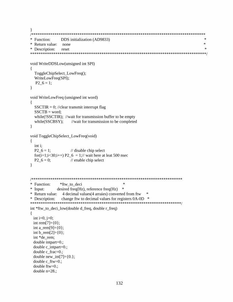
132
/************************************************** ********************************* * Function: DDS initialization (AD9833) * * Return value: none * * Description: reset * *************************************************** *********************************/ void WriteDDSLow(unsigned int SPI) ToggleChipSelect_LowFreq(); WriteLowFreq(SPI); P2_6 = 1; void WriteLowFreq (unsigned int word) SSCTIR = 0; //clear transmit interrupt flag SSCTB = word; while(!SSCTIR); //wait for transmission buffer to be empty while(SSCBSY); //wait for transmission to be completed void ToggleChipSelect_LowFreq(void) int i; P2_6 = 1; // disable chip select for(i=1;i<30;i++) P2_6 = 1;// wait here at leat 500 nsec P2_6 = 0; // enable chip select /************************************************** ********************** * Function: *ftw_to_deci * * Input: desired freq(Hz), reference freq(Hz) * * Return value: 4 decimal values(4 arraies) converted from ftw * * Description: change ftw to decimal values for registers 0A-0D * *************************************************** *********************/ int *ftw_to_deci_low(double d_freq, double r_freq) int i=0, j=0; int rem[7]=0; int a_rem[9]=0; int b_rem[2]=0; int *de_rem; double intpart=0.; double c_intpart=0.; double c_frac=0.; double new_int[7]=0.; double c_ftw=0.; double ftw=0.; double n=28.;
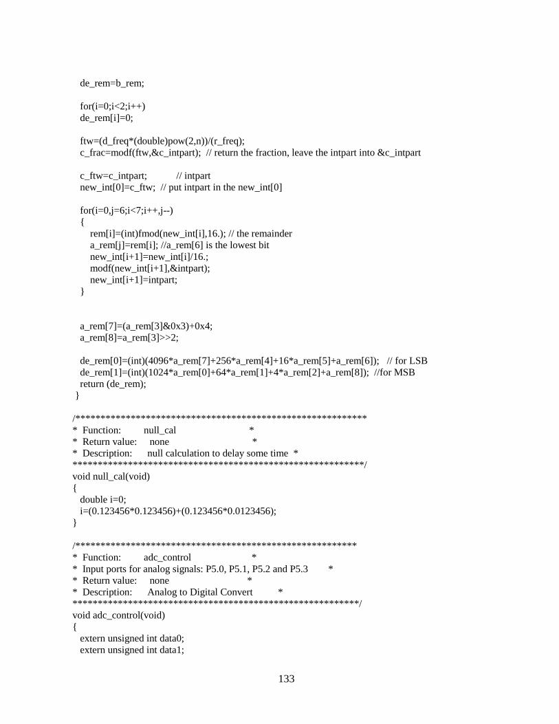
133
de_rem=b_rem; for(i=0;i<2;i++) de_rem[i]=0; ftw=(d_freq*(double)pow(2,n))/(r_freq); c_frac=modf(ftw,&c_intpart); // return the fraction, leave the intpart into &c_intpart c_ftw=c_intpart; // intpart new_int[0]=c_ftw; // put intpart in the new_int[0] for(i=0,j=6;i<7;i++,j--) rem[i]=(int)fmod(new_int[i],16.); // the remainder a_rem[j]=rem[i]; //a_rem[6] is the lowest bit new_int[i+1]=new_int[i]/16.; modf(new_int[i+1],&intpart); new_int[i+1]=intpart; a_rem[7]=(a_rem[3]&0x3)+0x4; a_rem[8]=a_rem[3]>>2; de_rem[0]=(int)(4096*a_rem[7]+256*a_rem[4]+16*a_rem[5]+a_rem[6]); // for LSB de_rem[1]=(int)(1024*a_rem[0]+64*a_rem[1]+4*a_rem[2]+a_rem[8]); //for MSB return (de_rem); /************************************************** ******** * Function: null_cal * * Return value: none * * Description: null calculation to delay some time * *************************************************** *******/ void null_cal(void) double i=0; i=(0.123456*0.123456)+(0.123456*0.0123456); /************************************************** ****** * Function: adc_control * * Input ports for analog signals: P5.0, P5.1, P5.2 and P5.3 * * Return value: none * * Description: Analog to Digital Convert * *************************************************** ******/ void adc_control(void) extern unsigned int data0; extern unsigned int data1;

134
extern unsigned int data2; extern unsigned int data3; ADCON=0XF023; //ADC conversion time control(ADCTC)=11 // -> Conversion clock(t_BC)=fcpu/8 //ADC sample time control(ADSTC)=11 // -> Sample clock(tsc)=t_BC*64 //ADC wait for read control(ADWR)=0 //ADC start bit(ADST)=0 //ADC mode selection(ADM)=10 // -> Auto scan single conversion //ADC Analog channel input selection(ADCH)=0011, sampling sequence of Channels 3,2,1 and 0. ADCIC=0; //initializing ADC interruupt control ADST=1; //ADC starts while(ADCIR==0); data3=ADDAT; //read an ADC result for thermocouple(P5.3) ADCIR=0; while(ADCIR==0); data2=ADDAT; //read an ADC result for thermistor(P5.2) ADCIR=0; while(ADCIR==0); data1=ADDAT; //read an ADC result for phase(P5.1) ADCIR=0; while(ADCIR==0); data0=ADDAT; //read an ADC result for gain(P5.0) /************************************************* **** * Function: timer_init * * Return value: none * * Description: initialize timer 3 * * Timer 3 is used for the delay * * This function was modified from Dr. Nelison's * *************************************************** **/ void timer_init(void) T3CON=0x0087; //T3UDE=0,T3UD=1 -> count down //Timer 3 run bit(T3R)=0 //Timer 3 mode control(T3M)=000 -> Timer Mode //Timer 3 Input Selection(T3I)=111 -> 19.531kHz T3=0; //Timer 3 register T3IC=0; //Interrupt Request Flag(T3IR)=0 //Interrupt Enable Bit(T3IE)=0 //Interrupt Priority Level(ILVL)=0000 //Group Level(GLVL)=00

135
/************************************************** ************************** * Function: delay_time * * Input: time to be delayed with the unit of msec * * Return value: none * * Description: delay time with the unit of msec (about 3000msec max.) * * Timer 3 is used for the delay * * This function was modified from Dr. Nelison's * *************************************************** *************************/ void delay_time(unsigned int value) timer_init(); if(value < 1) value=1; if(value > 3355) value=3355; T3=value*19; T3R=1; while(T3IR==0); T3R=0; /************************************************** ***************** * Function: io_up * * Return value: none * * Description: active I/O update clock and low * * null_cal function is used. * *************************************************** ****************/ void io_up(void) // for AD9858, it's the similar pin with FUD P6=0XC0; // P6.6(FUD update) active (high), P6.7(SPMODE) high null_cal(); null_cal(); null_cal(); P6=0X80; // P6.6(FUD update) low, P6.7(SPMODE) high /************************************************** ***************** * Function: control_register_init * * Return value: none * * Description: initialize MRESET and control registers * * io_up function is used. * *************************************************** ****************/ void control_register_init(void) P6=0XA0; // Profile 0, P6.5(RESET) active (high), P6.6(I/O update) low, P6.7(SPMODE) high null_cal(); // null calculation to delay short time for writing P6 = 0x80; // Profile 0, P6.5(RESET) low, P6.6(I/O update) low, P6.7(SPMODE) high P2=0XC0F8; // address 00 and P2.6((WRB)') high, P2.7((RDB)') high P7=0x58; // 2GHz Divider disabled, mixer and phase detect power down active

136
P2=0X80F8; // P2.7((RDB)') high, P2.6(WRB)' active (low) to move the data to I/O buffer null_cal(); // null calculation to delay short time for writing P2=0XC0F8; // P2.6(WRB)' high to stop writing, P2.7((RDB)') high io_up(); P2=0XC1F8; // address 01 and P2.6((WRB)') high, P2.7((RDB)') high P7=0x40; // Freq.sweep disabled, sine output enabled P2=0X81F8; // P2.7(RDB)' high, P2.6(WRB)' active (low) to move the data to I/O buffer null_cal(); // null calculation to delay short time for writing P2=0XC1F8; // P2.6(WRB)' high to stop writing, P2.7((RDB)') high io_up(); /************************************************** **************************** * Function: frequency * * Input: desired freq(Hz), reference freq(Hz) * * Return value: none * * Description: display the sinusoidal signal with the desired frequency * * *ftw_to_deci function is used * *************************************************** ***************************/ void frequency(double d_freq, double r_freq) int *ftw_freq; ftw_freq=ftw_to_deci(d_freq, r_freq); // convert desired frequency to FTW P2 = 0xCA78; // address 0A (ftw 1[7:0]), P2.6((WRB)') high, P2.7((RDB)') high P7=ftw_freq[3]; // data for ftw 1[7:0] P2 = 0X8A78; // P2.7((RDB)') high, P2.6(WRB)' active (low) to move the data to I/O buffer null_cal(); // null calculation to delay short time for writing P2 = 0XCA78; // P2.6(WRB)' high to stop writing, P2.7((RDB)') high io_up(); P2 = 0xCB78; // address 0B (ftw 1[15:8]) and P2.6((WRB)') high P7=ftw_freq[2]; // data for ftw 1[15:8] P2=0X8B78; // P2.7((RDB)') high,P2.6(WRB)' active (low) to move the data to I/O buffer null_cal(); // null calculation to delay short time for writing P2=0XCB78; // P2.6(WRB)' high to stop writing, P2.7((RDB)') high io_up(); P2 = 0xCC78; // address 0C (ftw 1[23:16]) and P2.6((WRB)') high P7=ftw_freq[1]; // data for ftw 1[23:16] P2=0X8C78; // P2.7((RDB)') high,P2.6(WRB)' active (low) to move the data to I/O buffer null_cal(); // null calculation to delay short time for writing P2=0XCC78; // P2.6(WRB)' high to stop writing, P2.7((RDB)') high io_up(); P2 = 0xCD78; // address 0D (ftw 1[31:24]) and P2.6((WRB)') high P7=ftw_freq[0]; // data for ftw 1[31:24] P2=0X8D78; // P2.7((RDB)') high,P2.6(WRB)' active (low) to move the data to I/O buffer null_cal(); // null calculation to delay short time for writing

137
P2=0XCD78; // P2.6(WRB)' high to stop writing, P2.7((RDB)') high io_up(); /************************************************** ********************** * Function: *ftw_to_deci * * Input: desired freq(Hz), reference freq(Hz) * * Return value: 4 decimal values(4 arraies) converted from ftw * * Description: change ftw to decimal values for registers 0A-0D * *************************************************** *********************/ int *ftw_to_deci(double d_freq, double r_freq) int i=0, j=0; int rem[8]=0; int a_rem[8]=0; int b_rem[4]=0; int *de_rem; double intpart=0.; double c_intpart=0.; double c_frac=0.; double new_int[9]=0.; double c_ftw=0.; double ftw=0.; double n=32.; de_rem=b_rem; for(i=0;i<4;i++) de_rem[i]=0; ftw=(d_freq*(double)pow(2,n))/(r_freq); c_frac=modf(ftw,&c_intpart); c_ftw=c_intpart; new_int[0]=c_ftw; for(i=0,j=7;i<8;i++,j--) rem[i]=(int)fmod(new_int[i],16.); a_rem[j]=rem[i]; new_int[i+1]=new_int[i]/16.; modf(new_int[i+1],&intpart); new_int[i+1]=intpart; de_rem[0]=(int)(16*a_rem[0]+a_rem[1]); de_rem[1]=(int)(16*a_rem[2]+a_rem[3]); de_rem[2]=(int)(16*a_rem[4]+a_rem[5]); de_rem[3]=(int)(16*a_rem[6]+a_rem[7]); return (de_rem);

138
/************************************************** *********************** * Function: collect_data * * Input: none * * Return value: none * * Description: collecting data of gain,phase,current * *************************************************** *********************/ void collect_data(void) unsigned char rt; unsigned int tgain[3]=0; unsigned int tphase[3]=0; unsigned int tthermistor[3]=0; unsigned int tthermocouple[3]=0; double thermistor=0; double thermocouple=0; unsigned int thermistor_1=0; unsigned int thermocouple_1=0; double V_thermistor=0; double R_thermistor=0; double T_thermistor=0; long double T_thermocouple=0; double V_thermocouple=0; double V_thermocouple_1=0; int T_thermocouple_P=0; int T_thermistor_P=0; double A=1.92E-3; double B=9.86315E-5; double C=6.6032E-7; double D=0; double F=0; for(rt=0;rt<3;rt++) adc_control(); //A/D conversion tgain[rt]=data0; //digitized value for gain tphase[rt]=(data1-4096); //digitized value for phase tthermistor[rt]=(data2-8192); tthermocouple[rt]=(data3-12288); gain=(int)((tgain[0]+tgain[1]+tgain[2])/3); //calculating the average value of three digital values for gain phase=(int)((tphase[0]+tphase[1]+tphase[2])/3); //calculating the average value of three digital values for phase thermistor=(float)((tthermistor[0]+tthermistor[1]+tthermistor[2])/3);

139
//calculating the average value of three digital values for thermistor thermocouple=(float)((tthermocouple[0]+tthermocouple[1]+tthermocouple[2])/3); //calculating the average value of three digital values for thermocouple thermistor_1=(int)thermistor; thermocouple_1=(int)thermocouple; V_thermistor=thermistor*5.075/1024; R_thermistor=10000*V_thermistor/(5-V_thermistor); F=log(R_thermistor); T_thermistor=1/(A+B*F+C*pow(F,3))-274.4; V_thermocouple_1=thermocouple*5.075/1024; V_thermocouple=(thermocouple*5.075/1024-2.5087+Temp-0.007)/101; D=V_thermocouple; T_thermocouple=0.100860910+25727.94369*D-767345.8295*pow(D,2)+78025595.81*pow(D,3)- 9.247486589E9*pow(D,4)+6.97688E11*pow(D,5)-2.66192E13*pow(D,6)+3.94078E14*pow(D,7); T=(int)((T_thermistor+T_thermocouple)*10); printf(" %d, %d, %d, %d, %d \n",gain,phase,thermistor_1,thermocouple_1,T); //downloading data for gain, phase, and current /************************************************** ************************ * Function: collect_data * * Input: none * * Return value: none * * Description: collecting data of gain,phase,themistor, thermocouple * *************************************************** ***********************/ void collect_data_T(void) unsigned char rt; unsigned int tthermocouple[3]=0; double thermocouple=0; double V_thermistor=0; double V_thermocouple=0; for(rt=0;rt<3;rt++) adc_control(); //A/D conversion tthermocouple[rt]=(data3-12288); thermocouple=(float)((tthermocouple[0]+tthermocouple[1]+tthermocouple[2])/3); //calculating the average value of three digital values for thermocouple V_thermocouple=thermocouple*5.075/1024; Temp=(double) (2.509-V_thermocouple);