A PHYSICS-BASED HETEROJUNCTION BIPOLAR TRANSISTOR … · AFIT/GE/ENG/93D-07 AD-A274 081 A...
251
AFIT/GE/ENG/93D-07 AD-A27 4 081 A PHYSICS-BASED HETEROJUNCTION BIPOLAR TRANSISTOR MODEL FOR INTEGRATED CIRCUIT SIMULATION THESIS James A. Fellows D TIC Captain, USAF T " E- AFIT/GE/ENG/93D-07 DEC2 3 1993 Approved for public release; distribution unlimited • 93-31019 93 12 22 132 13-3109111 marin m mmal • iman mHiIl~ ~l
Transcript of A PHYSICS-BASED HETEROJUNCTION BIPOLAR TRANSISTOR … · AFIT/GE/ENG/93D-07 AD-A274 081 A...

AFIT/GE/ENG/93D-07
AD-A27 4 081
A PHYSICS-BASED HETEROJUNCTION BIPOLAR TRANSISTORMODEL FOR INTEGRATED CIRCUIT SIMULATION
THESIS
James A. Fellows D TICCaptain, USAF T " E-
AFIT/GE/ENG/93D-07 DEC2 3 1993
Approved for public release; distribution unlimited
• 93-3101993 12 22 132 13-3109111
marin m mmal • iman mHiIl~ ~l

BestAvailable
Copy

AFIT/GE/ENG/93D-07
A PHYSICS-BASED HETEROJUNCTION BIPOLAR TRANSISTOR
MODEL FOR INTEGRATED CIRCUIT SIMULATION
THESIS
Presented to the Faculty of the Graduate School of Engineering
of the Air Force Institute of Technology
Air University
In Partial Fulfillment of the
Requirements for the degree of
Master of Science in Electrical F-gineering
Accesion For
NTIS CRA&IDTIC TABUnannouncedJustification
James A. Fellows, B.S.E.E By
Captain, USAF Availability Codes
Sus-- IAvala, -••Special
December 1993
Approved for public release; distribution unlimited D TIcCopyy

Acknowvodgements
I would like to thank my loving and selfless wife for her support
and patience during this thesis effort. Her helpfulness at home and with
our daughter Elise is deeply appreciated. This has been a challenging
time for both of us, and she deserves far more credit than she has
received.
I would like to thank my thesis advisor, Dr. Victor M. Bright, for
his guidance, instruction, and encouragement. The many hours we spent at
his whiteboard were invaluable in helping me to understand semiconductors.
I would like to thank Dr. Burhan Bayraktaroglu and Dr. Chern Huang of
WL/ELR. I e- thankful for the measured data and geometry information
provided b. Bayraktaroglu. I appreciate the time and wisdom that they
both shared with me through several insightful discussions on HBTs. I
would also like to thank Captain Thomas Jenkins for the time he spent
instructing me on operating the HP4145B, semiconductor parameter analyzer,
as well as for the discussions on semiconductor device physics.
ii

Table of Contents
List of Figures ............... ......................... .... vii
List of Tables ....................... .......................... x
List of Symbols ...................... .......................... xi
1. Introduction ..................... ......................... 1
1.1 Background ................ ........................ . .. 1
1.2 Problem Statement ................. ..................... 9
1.3 Summary of Current Knowledge ........ ............... ... O10
1.3.1 Large-Signal Modeling ............ ................. 10
1.3.2 Small-Signal Modeling ......... ................. .... 11
1.4 Assumptions and Scope ........... ................... ... 12
1.5 Approach .................. ......................... ... 14
1.6 Thesis Overview ............... ...................... ... 17
2. Literature Review ............ ....................... .... 18
2.1 Large-Signal Modeling ........... ................... ... 21
2.1.1 Ryum and Abdel-Motaleb .......... ................ ... 21
2.1.2 Parikh and Lindholm ......... .................. ... 22
2.1.3 Grossman and Oki ............ ................... ... 24
2.1.4 Grossman and Choma ........... .................. ... 26
2.1.5 Hafizi et al ............ ...................... ... 26
2.2 Small-Signal Modeling ........... ................... ... 29
2.2.1 Pehlke and Pavlidis ......... .................. ... 29
2.2.2 Maas and Tait ............ ..................... ... 30
iii

2.2.3 Trew et al . . . . . . . . . . . . . . . . . . . . . . . 31
2.2.4 Costa at al ............. ...................... ... 31
2.3 Summary of Literature ........... ................... ... 33
3. Theory ..................... ............................ ... 35
3.1 Physical Large-Signal Modeling ...... .............. ... 35
3.2 Linearization ............. ....................... .... 48
3.3 Physical Small-Signal Modeling. ..... .............. ... 52
3.4 S-Parameters ................ ....................... ... 54
4. Methodology ................ .......................... ... 58
4.1 Knowledge of Device Material ........ ............... ... 58
4.2 Knowledge of Device Geometry ........ ............... ... 63
4.3 Knowledge of the Fabrication Process ........ ........... 66
4.4 Determination of SPICE Model Parameters .... .......... .. 67
4.4.1 Forward base transit time, TF ..... ............. ... 68
4.4.2 Maximum forward common-emitter current gain, BF . . .. 70
4.4.3 Minority carrier lifetime in the base, ......... 74
4.4.4 Leakage saturation currents, ISE and ISC .. ....... .. 77
4.4.5 Transport saturation current, IS and reverse parameters,
BR and TR .................. ....................... 78
4.4.6 Junction grading factors, MJE and MJC ... ......... ... 78
4.4.7 Built-in junction voltages, VJE and VJC ........... ... 79
4.4.8 Zero-bias depletion capacitances, CJE and CJC ... ..... 79
4.4.9 Internal capacitance ratio, XCJC . . . ......... 79
4.4.10 Emitter series resistance, RE ...... ............ .. 80
4.4.11 Base series resistance, RB ....... .............. ... 81
iv

4.4.12 Collector series resistance, RC .... ........... ... 82
4.4.13 Ideality factors, NF, NR, NE, and NC ... ......... ... 83
4.4.14 Corner for high current OF degradation, IKF ..... .. 83
4.5 SPICE dc Simulation ........... .................... ... 84
4.6 SPICE ac Simulation ............. .................... .. 85
4.7 Adding Parasitics to the Small-signal Equivalent Circuit 87
5. Results and Discussion .............. .................... .. 95
5.1 DC Results .................. ........................ ... 96
5.1.1 3uldlf and 3u5dlf Device dc Results .... .......... ... 98
5.1.2 2u6d2f Device dc Results ...... .............. ... 109
5.2 Microwave Results ............. .................... ... 116
5.2.1 General S-parameter contours .... ............ ... 116
5.2.2 Comparison of modeled and measured S-parameters . . 117
5.2.3 Model parameter sensitivity analysis .. ........ .. 135
6. Conclusions and Recommendations ....... ............... ... 147
Appendix A: Mathcad Files ............ ................... ... A-1
Appendix B: HSPICE Files .............. .................... ... B-1
DC HSPICE Files ............. ....................... . ... B-2
Microwave HSPICE Files ............ ................... ... B-5
HSPICE Optimization Files ........... .................. . .. B-9
HSPICE 2u6d2f ac Analysis Script ....... .............. ... B-13
Bibliography ..................... ......................... Bib-l
V

List of Fiqures
Figure 1.1 Representative layer structure of an npn BJT [13:171]. 3
Figure 1.2 Typical doping profile of an npn BJT [14:146] .... ...... 3
Figure 1.3 Energy bandgap diagram of a forward-biased npn BJT [15:3361.4
Figure 1.4 Representative layer structure for an npn AlGaAs/GaAs HBT(15:373] ................. ........................... 4
Figure 1.5 Typical doping profile of an Npn AlGaAs/GaAs HBT. 5
Figure 1.6 Energy bandgap diagram of an abrupt-emitter forward-biasedNpn AlGaAs/GaAs HBT [16:198]1 .......... ................. 5
Figure 1.7 Large-signal junction transistor equivalent circuit[21:61]. ..................... ........................... 7
Figure 1.8 Hybrid-w small-signal junction transistor equivalent circuit[21:68] ...................... ........................... 7
Figure 2.1 The basic npn bipolar transistor Ebers-Moll equivalentcircuit [21:41] ............ ....................... .... 20
Figure 2.2 An npn bipolar transistor Gummel-Poon equivalent circuit
[44:207] ............... ........................... ... 20
Figure 2.3 Gummel plot for a BJT showing model parameters [26:2123]. 28
Figure 2.4 An extended EM large-signal equivalent circuit [26:2122]. 28
Figure 2.5 Pehlke's small-signal T-model equivalent circuit [28:2368].32
Figure 2.6 Maas' small-signal equivalent circuit [29:502]..... ... 32
Figure 3.1 Homojunction (a) and heterojunction (b) band diagrams atequilibrium .............. ......................... .... 39
Figure 3.2 Ebers-Moll equivalent circuit modified to include junctioncapacitances ............. ......................... ... 42
Figure 3.3 Lateral view of an HBT showing emitter resistance, RE, andthe three components of base resistance, RB . . . .. . . . . .. . . . 4 2
Figure 3.4 The complete large-signal equivalent circuit .... ...... 46
Figure 3.5 Intermediate circuit in the derivation of the SPICE large-signal equivalent circuit .............. .................. 46
vi

Figure 3.6 Complete SPICE large-signal equivalent circuit showingcomponents of IB and Ic .......... ................... ... 47
Figure 3.7 Pnp junction transistor modes of operation and associatedminority carrier concentrations (51:1221 .... ........... ... 50
Figure 3.8 (a) Relationship between load line, bias point and modes ofoperation and (b) corresponding digital switching circuit[51:139] ................ ........................... ... 50
Figure 3.9 (a) Common-base circuit configuration, (b) emitter currentpulse and (c) corresponding collector current responseillustrating trancistor switching times [14:179] .... ....... 51
Figure 3.10 The hybrid-ir small-signal equivalent circuit .......... 55
Figure 3.11 Two-port S-parameter flow graph [54:221] ......... .. 55
Figure 4.1 Mask layout of a 3u5dlf AlGaAs HBT [60] ..... ......... 65
Figure 4.2 Lateral view of 3u5dlf HBT geometry .............. .... 65
Figure 4.3 Top view of emitter and base contacts showing the dotgeometry ............... ........................... ... 67
Figure 4.4 Energy bandgap diagram of a forward-biased Npn AlGaAs/GaAsHBT showing current components. [17:15]. .... ........... ... 72
Figure 4.5 Lateral view of HBT showing the base-collector depletioncapacitance distributed across the base series resistance. . 80
Figure 4.6 SPICE junction transistor dc testbench ... ......... ... 86
Figure 4.7 SPICE junction transistor ac testbench ... ......... ... 86
Figure 4.8 HSPICE hybrid-i small-signal equivalent circuit with base-collector depletion capacitance distributed across the baseresistance ............... .......................... ... 88
Figure 4.9 Small-signal hybrid-w equivalent circuit complete withparasitic elements ............ ...................... ... 88
Figure 4.10 Top-view of the simplified base metallization geometry fora single emitter dot ............ ..................... ... 93
Figure 4.11 Annotated diagram of fringing capacitance between twoconductors lying in the same plane ...... .............. ... 93
Figure 5.1 Plot of BF versus Ic with linear regression showing regionof nearly constant BF for the 3uldlf device .......... . i.. 100
Figure 5.2 Plot of BF versus Ic with linear regression showing regionof nearly constant BF for the 3u5dlf device .......... . i.. 100
vii

Figure 5.3 I-V characteristics for the 3uldlf device with Is swept in20 MA increments ............ ...................... ... 101
Figure 5.4 Reverse I-V characteristics for the 3uldlf device with Isswept in 20 MA increments ....... ................. .... 101
Figure 5.5 I-V characteristics for the 3u5dlf device with IB swept in50 MA increments ............ ...................... ... 105
Figure 5.6 Reverse I-V characteristics for the 3u5dlf device with IDswept in 50 MA increments ....... ................. .... 105
Figure 5.7 Magnitude of the percent difference between modeled andmeasured Ic averaged over all ten IB curves .. ........ .. 107
Figure 5.8 Magnitude of the percent difference between modeled andmeasured Ic averaged over all ten I curves .. ........ .. 107
Figure 5.9 I-V characteristics for the 2u6d2f device with variable BFin SPICE and IB swept in 100 pA increments ........... .i... 110
Figure 5.10 Curve fit expression for BF as a function of base currentfor the 2u6d2f device .............. ................... 110
Figure 5.11 I-V characteristics for the 2u6d2f device with IB swept in100 MA increments ............ ..................... ... 113
Figure 5.12 Reverse I-V characteristics for the 2u6d2f device with IBswept in 100 MA increments ...... ................. .... 113
Figure 5.13 Percent difference between modeled and measured IC for the
2u6d2f device at IB - 800 MA ......... ................ 115
Figure 5.14 Comparison of S11 for the 3uldlf device from 1 to 50 GHz. 119
Figure 5.15 Comparison of S12 for the 3uldlf device from 1 to 50 GHz. 119
Figure 5.16 Comparison of S21 for the 3uldlf device from 1 to 50 GHz. 120
Figure 5.17 Comparison of S22 for the 3uldlf device from 1 to 50 GHz. 120
Figure 5.18 Comparison of S1, for the 3uSdlf device from 1 to 50 GHz. 124
Figure 5.19 Comparison of S12 for the 3uSdlf device from 1 to 50 GHz. 124
Figure 5.20 Comparison of S21 for the 3uSdlf device from 1 to 50 GHz. 125
Figure 5.21 Comparison of S22 for the 3uSdlf device from 1 to 50 GHz. 125
Figure 5.22 Comparison of S1, for the 2u6d2f device from 1 to 50 GHz. 128
Figure 5.23 Comparison of S12 for the 2u6d2f device from 1 to 50 GHz. 128
viii

Figure 5.24 Comparison of S21 for the 2u6d2f device from 1 to 50 GHz. 129
Figure 5.25 Comparison of S22 for the 2u6d2f device from 1 to 50 GHz. 129
Figure 5.26 Percent difference between the modeled and measuredmagnitude of Sn1 for the 2u6d2f device at a 1 V, 800 AA bias. 131
Figure 5.27 Percent difference between the modeled and measured angleof S$1 for the 2u6d2f device at a 1 V, 800 pA bias. ..... 131
Figure 5.28 Percent difference between the modeled and measuredmagnitude of S22 for the 2u6d2f device at a 1 V, 800 uA bias. 132
Figure 5.29 Percent difference between the modeled and measured angleof S22 for the 2u6d2f device at a 1 V, 800 IA bias. ..... 132
Figure 5.30 Percent difference between the modeled and measuredmagnitude of S12 for the 2u6d2f device at a 1 V, 800 juA bias. 133
Figure 5.31 Percent difference between the modeled and measuredmagnitude of S21 for the 2u6d2f device at a 1 V, 800 pA bias. 133
Figure 5.32 Comparison of S1, for the 2u6d2f device from 1 to 50 GHzwith optimized parasitics ....... ................. .... 143
Figure 5.33 Comparison of S12 for the 2u6d2f device from 1 to 50 GHzwith optimized parasitics ....... ................. .... 143
Figure 5.34 Comparison of S21 for the 2u6d2f device from 1 to 50 GHzwith optimized parasitics ....... ................. .... 144
Figure 5.35 Comparison of S2 for the 2u6d2f device from 1 to 50 GHzwith optimized parasitics ....... ................. .... 144
ix

List of Tables
Table 3-1 SPICE BIT Model Parameters ...... ................ .. 48
Table 4-1 General Constants Used in Calculations .............. .. 59
Table 4-2 Material Parameters and Expressions Used inCalculations .............. ....................... .61
Table 4-3 Mobility Parameter Values for GaAs ..... ............ .. 62
Table 4-4 Layer Doping Profile for the 3u5dlf Device ........... .. 67
Table 4-5 Calculated Values of Minority Electron Bulk BaseRecombination Lifetimes ......... ................. .. 75
Table 5-1 Definitions for Qualitative Model Performance ........ .. 96
Table 5-2 3uldlf SPICE BJT dc Model Parameters .... ........... .104
Table 5-3 3u5dlf SPICE BJT dc Model Parameters .... ........... .104
Table 5-4 Optimized Parameters for the 2u6d2f Device .... ....... 112
Table 5-5 4i6d2f SPICE BJT dc Model Parameters. ............. .. 112
Table 5-6 3uldlf SPICE LJT Full Model Parameters ............ ... 118
Table 5-7 3u5dlf SPICE BJT Full Model Parameters ............ ... 123
Table 5-8 2u6d2f SPICE BJT Full Model Parameters ............ ... 127
Table 5-9 Sensitivity of Cbcp on S-parameters .... ........... ... 136
Table 5-10 Sensitivity of Cb.p on S-parameters .... ........... ... 136
Table 5-11 Sensitivity of Cop on S-parameters .... ........... ... 137
Table 5-12 Sensitivity of CJC on S-parameters .... ........... ... 137
Table 5-13 Sensitivity of Lp on S-parameters .... ........... .. 138
Table 5-14 Sensitivity of Lp on S-parameters .... ........... .. 138
Table 5-15 Sensitivity of L4p on S-parameters .... ........... .. 138
Table 5-16 Comparison of 2u6d2f Parasitics with other HBT Models 142
Table 5-17 Optimized Parasitics for the 2u6d2f Device .... ....... 142
Table 5-18 Various HBT SPICE Model Parameters .... ........... ... 147
x

List of Symbols
a 1 Radius of the emitter dot (cm).
a2 Inner radius of the base contact (cm).
a3 Approximate outer radius of the base contact (cm).
A Any generic area (cm 2 ).
Ab* Area of the base-emitter junction (cm 2 ).
Abc Area of the base-collector junction (cm 2 ).
Ap Auger recombination coefficient (cm6 .s- 1 ).
a Caughey-Thomas mobility curve fit parameter.
CkF Forward common-base current gain.
CkR Reverse common-base current gain.
L Angle of an S-parameter in polar form.
Bn Radiative recombination coefficient (cm3 .s-l).
BF Ideal maximum forward common-emitter current gain.
BR Ideal maximum reverse common-emitter current gain.
16F Forward common-emitter current gain.
Reverse common-emitter current gain.
Base transport factor.
CBE Total base-emitter capacitance (F).
BC• Total base-collector capacitance (F).
CJE Base-emitter zero-bias depletion capacitance (F).
CJC Base-collector zero-bias depletion capacitance (F).
Ci Generic depletion capacitance (F).
Cjs Base-emitter depletion capacitance (F).
CjC Base-collector depletion capacitance (F).
xi

Cd Generic diffusion capacitance (F).
Cd. Base-emitter diffusion capacitance (F).
Cdc Base-collector diffusion capacitance (F).
Cý Total small-signal base-emitter capacitance (F).
CA Total small-signal base-collector capacitance (F).
Cbep Base-emitter parasitic capacitance (F).
Cbcp Base-collector parasitic capacitance (F).
Coep Collector-emitter parasitic capacitance (F).
cbcdep Internal base-collector depletion capacitance (F).
cbcx External base-collector depletion capacitance (F).
Cgint Total internal base-collector small-signal capacitance (F).
Csext Total. external base-collector small-signal capacitance (F).
d Generic thickness of dielectric between two conductors (cm).
Dp, Dn Minority hole and electron diffusivities (cm2.s- 1).
DpE, DPC Minority hole diffusivities in the emitter andcollector (cm2 .s-1).
DnB Minority electron diffusivity in the base (cm2 .s- 1).
E$Gas Bandgap energy of intrinsic GaAs (eV).
AEgB Bandgap narrowing in the GaAs base due to high doping (eV).
ESE Bandgap energy of the AlGaAs emitter (eV).
E5 B Bandgap energy of the GaAs base (eV).
AE Bandgap difference between the emitter and base (eV).
Co Permittivity in vacuum (F.cm- 1).
4E, Generic semiconductor permittivity (F-cm-1).
CGaAs Relative permittivity of GaAs.
CAlGas Relative permittivity of the AlGaAs emitter.
CE Permittivity of the emitter (Fcm-1 ).
xii

Permittivity of the base (F-cm- 1 ).
6p Permittivity of polyimide (F.cm- 1 ).
FEN Thermionic electron flux across an abrupt base-emitterheterojunction (c- 2 .s- 1 ).
f Frequency (Hz).
fT Unity current-gain cutoff frequency (Hz).
Maximum frequency of oscillation (Hz).
Small-signal base-emitter junction conductance (S).
g1% Small-signal base-collector junction conductance (S).
g0 Small-signal transistor common-emitter output conductance (S).
gm Small-signal transconductance (S).
r Reflection coefficient of a transmission line.
'Y Emitter injection efficiency.
IKF Corner for high current OF degradation (A).
IKR Corner for high current OR degradation (A).
IE Total current through emitter terminal (A).
IB Total current through base terminal (A).
Ic Total current through collector terminal (A).
IES Base-emitter junction saturation current (A).
Ics Base-collector junction saturation current (A).
Icc Current through the base-collector junction due to the base-emitter voltage (A).
IEC Current through the base-emitter junction due to the base-collector voltage (A).
ICT Total current through the transistor from collector to emitter(A).
IS Transport saturation current (A).
ISE Base-emitter recombination saturation current (A).
ISC Base-collector recombination saturation current (A).
xiii

Ic, Electron current from the base into the collector (A).
Ip Hole current injected from the base into the emitter (A).
in Electron current injected from the emitter into the base (A).
I, Electron current lost to SCR recombination (A).
Ir Electron current lost to bulk base recombination (A).
I, Ideal base-collector drift-diffusion current (A).
12 Ideal base-emitter drift-diffusion current (A).
13 Total base-collector recombination current (A).
14 Total base-emitter recombination current (A).
Izec Generic recombination current (A).
k Boltzmann's constant (eV.K-1 ).
lee Diameter of an emitter dot (cm).
L Any generic length (cm).
IP, IL Minority hole and electron diffusion lengths (cm).
IVE, Lpc Minority hole diffusion lengths in the emitter andcollector (cm).
LnB Minority electron diffusion length in the base (cm).
LE Length of a rectangular emitter finger (cm).
Is Length of a rectangular base finger (cm).
Lint Internal inductance (H).
Lext External inductance (H).
Lbp Base parasitic series inductance (H).
L.P Emitter parasitic series inductance (H).
LCP Collector parasitic series inductance (H).
ILr Semiconductor/metal contact characteristic length (cm).
m Number of base or collector fingers in parallel.
MO Electron rest mass (Kg).
xiv

Mn Effective mass of an electron in GaAs (Kg).
WUE Base-emitter junction grading factor.
MJC Base-collector junction grading factor.
IMI Magnitude of an S-parameter in polar form.
/4o Permeability in vacuum (H-cm- 1).
An, Ap Generic electron and hole mobilities (cm2 .K.eV- 1.s- 1).
AMM Maximum mobility for a particular carrier (cm2 .K.eV-1 -s- 1)
PZmtn Minimum mobility for a particular carrier tcm2 .K.eV- 1.s-1 ).
ni Generic semiconductor intr .isic carrier concentration (cm- 3).
niGu Intrinsic carrier concentration of GaAs (cm- 3).
nj,, nic Intrinsic carrier concentration in the emitter andcollector (cm- 3).
niB Intrinsic carrier concentration in the base (cm- 3).
npo Equilibrium concentration of minority electrons (cm- 3).
np' (Wb) Concentration of excess minority electrons at the collectoredge of the neutral base region (cm- 3).
N Generic doping concentration (cm- 3).
Nref Caughey-Thomas mobility curve fit parameter.
NA Acceptor dopant concentration in p-material (cm-3 ).
ND Donor dopant concentration in n-material (cm- 3).
NE, NB, Nc Emitter, base, and collector dopant concentrations (cm- 3).
Nt Concentration of recombination centers in the base (cm- 3).
Na, NcD Conduction band density of states in the emitter andbase (cm- 3).
NvE, NvB Valence band density of states in the emitter and base (cm- 3).
NF Forward current emission coefficient.
NR Reverse current emission coefficient.
NE Base-emitter leakage emission coefficient.
xv

NC Base-collector leakage emission coefficient.
Generic non-ideal emission coefficient.
Ndot Number of emitter dots per finger.
Nf18 Number of base fingers.
Pno Equilibrium concentration of minority holes (cm-3).
q Electron charge (C).
qB Normalized base charge.
QB Total base charge (C).
01f Zero-bias base charge (C).
QVE Base-emitter junction depletion charge (C).
Qvc Base-collector junction depletion charge (C).
QF Forward injected base charge (C).
QR Reverse injected base charge (C).
RB Base series resistance (0).
Rc Collector series resistance (0).
RE Emitter series resistance (0).
RE SPICE BJT emitter resistance (0).
RB SPICE BJT internal base resistance (0).
RC SPICE BJT collector resistance (0).
RBint Internal base series resistance (0).
RBoxt External base series resistance (0).
RBSh Base layer sheet resistance (0/0).
Rcontact Metal/semiconductor contact resistance (Q).
Rt.1 Bulk semiconductor resistance (0).
R.p Spreading resistance (0).
R1c ]Lateral contact resistance (0).
R1*ak Semi-insulating GaAs leakage resistance (0).
xvi

p* Sheet resistance of a generic semiconductor layer (0/0).
pn, Pp n-type and p-type semiconductor resistivities (0-cm).
PAu Resistivity of gold metallization at 10 GHz (0.cm).
PC Generic specific contact resistance (0.cm2 ).
pep Specific contact resistance for a contact on p-typematerial (0-cm2 ).
Pen Specific contact resistance for a contact on n-typematerial (0-cm2 ).
SEN Effective base-emitter electron interface velocity (cm.s- 1 ).
ScN Effective base-collector electron interface velocity (cm-s- 1 ).
Snl Input reflection coefficient with the output matched to Z,.
S12 Reverse transmission or isolation coefficient.
S21 Forward transmission (gain or loss) coefficient.
S22 Output reflection coefficient with the input matched to Z,.
SE Rectangular emitter contact metallization width (cm).
SB Rectangular base contact metallization width (cm).
an Electron capture cross section (cm2 ).
t Generic thickness of a semiconductor or metal (cm).
T Absolute temperature (K).
TF Base forward transit time (s).
TR Base reverse transit time (s).
Tp, rn Lifecimes of excess minority holes and electrons (s).
TsR9 Shockley-Read-Hall recombination lifetime (s).
TAus Auger recombinea .,-n lifetime (s).
1 rad Radiative recombination lifetime (s).
Tee Emitter-to-collector majority carrier transit time (s).
Tno Excess minority electron recombination lifetime (s).
Excess minority hole recombination lifetime (s).
xvii

- 1 -- -- - ._,_ - ... -11 ý . i
U Generic recombination rate (cm73-s- 1 ).
Vbi Junction built-in voltage (V).
VJE Base-emitter built-in potential (V).
VJC Base-collector built-in potential (V).
VT Thermal voltage given by kT/q (V).
V÷ i+An ac voltage waveform incident to port j (V).
V- An ac voltage waveform reflected from port i due to the
driving signal at port j (V).
VU Externally applied base-emitter voltage (V).
VBC Externally applied base-collector voltage (V).
VIE' Internal voltage across the base-emitter junction (V).
VIBCc Internal voltage across the base-collector Junction (V).
U3,zo Small-signal base-emitter junction voltage (V).
uB, co Small-signal base-collector junction voltage (V).
V Generic externally applied voltage (V).
vbcx Distributed base-collector voltage (V).
vth Average thermal velocity for an electron (cm.s-').
vrat Electron saturation velocity in GaAs at 300 K (cm-s- 1).
vnB, vp Minority electron and hole diffusion velocities (cm.s- 1).
WB Zero-bias neutral base width (cm).
W Any generic width (cm).
Radian frequency.
V.The potential function of Poisson's equation (V).
x Mole fraction of Aluminum in AlXGa-,zAs.
X Generic depletion region thickness (cm).
XPE Thickness of base-emitter SCR in the p-type base (cm).
XPC Thickness of base-collector SCR in the p-type base (cm).
xviii

x Generic distance variable (cm).
X. Capacitive reactance (0).
XCJC Fraction of base-collector depletion capacitance internal tothe base.
zo The characteristic impedance of a transmission line (0).
ZL The load impedance connected to a transmission line (0).
xix

A PHYSICS- DASED NNTUROUNC•TION DIPOLRR TRUNSISYOR
MODEL FOR INTEGRATED CIRCUIT SIMULATION
1. Introduction
The purpose of this research effort was to derive a physics-based dc
model for a Heterojunction Bipolar Transistor (HBT). The dc model was
then linearized to arrive at a small-signal model that accurately predicts
the device's electrical behavior at microwave frequencies. This new model
offers features not found in previous analytical or physics-based IBT
models such as consideration of a cylindrical emitter-base geometry and is
direct implemention into SPICE (Simulation Program with Integrated Circuit
Emphasis). The device model parameters were determined from a knowledge
of the device material, geometry, and fabrication process. The model was
then developed by using semiconductor physics to calculate modified
parameters for the existing SPICE bipolar junction transistor (LIT) model.
1.1 Background
The design and fabrication of HBTs have received increased attention
in recent years. This attention is due primarily to the significantly
greater performance potential that can be obtained from HBTs compared to
the performance of traditional BJTs [1,2,31. The most technologically
mature HBTs are fabricated with Al 1 Ga1 _•As/GaAs [4,5,6,71, although many
other III-V compounds have been used (8,9,10,11]. Devices based on these
III-V compounds as well as Si/Sil-,JGe, devices [12], are distinguished
from homojunction devices by a wide energy bandgap emitter relative to the
base. Both BJTs and HBTs are junction transistors typically fabricated
with an n-type emitter and collector, and a p-type base. A representative
1

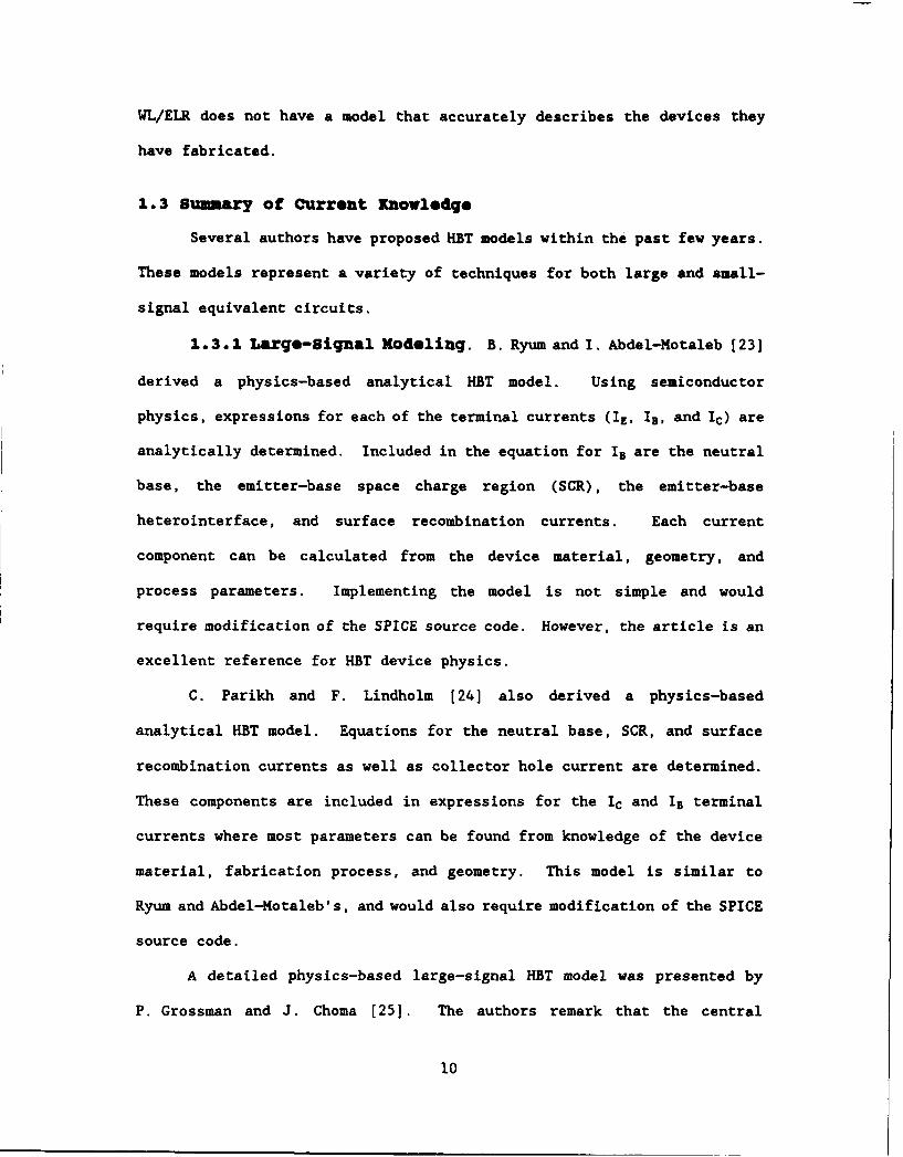
layer structure, doping concentration and energy bandgap diagram for an
npn BJT are shown in Figs. 1.1 - 1.3. The corresponding diagrams for an
Npn HBT are shown in Figs. 1.4 - 1.6. The capital "N" denotes a wide-gap
material.
BJTs are typically lateral or planar in structure, while HBTs are
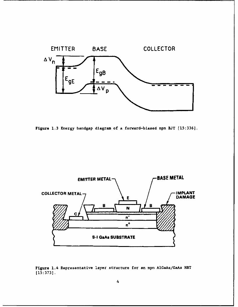
vertical devices, as seen in Figs. 1.1 and 1.4, respectively. Fig. 1.6
shows the energy band diagram for an Al.Ga1 .. ,As emitter / GaAs base Np
heterojunction. The most important feature of the heterojunction is that
it provides a larger barrier for holes attempting to move from the base to
the emitter than for electrons moving from the emitter to the base.
Consequently, the base of an HBT may be doped more heavily than the
emitter without sacrificing transistor efficiency. This new design
freedom is a direct result of the band gap difference and allows for
previously unobtainable device figure of merit improvements [17,18]. Most
notably, HBTs can be operated at higher speeds and with greater
efficiency. However, the trend toward optimizing device performance
requires a pattern for predicting device behavior.
The HBT is a relatively new device. Although HBTs were
conceptualized by W. Shockley in 1948 [19], the first HBT was not
fabricated until 1972 [20]. However, practical HBTs did not evolve until
the advent of Molecular Beam Epitaxy (MBE). MBE provided high crystalline
purity semiconductors, and the strict control over epitaxial layer
thickness and doping necessary for realizing the HBT's theoretical
performance potential.
Simulation is critical to furthering device technology, because it
provides device and integrated circuit design feedback. The purpose of
simulation is to accurately predict the electrical performance of either
2

SB EB
n+ buried layerp-type substrate
Figure 1.1 Representative layer structure of an npn BJT [13:171].
V ED VC 8
n+ p n DOPED nMITTE" BASE EPITAXIAL SUBSTRATE
toiA awet WC -
10 ZI -I
1 020
~109
~1018
z 101 A
i P
0~15
nn
0 10 15DISTANCE (M"m)
Figure 1.2 Typical doping profile of an npn BJT [14:1461.
3
EMITTER BASE COLLECTOR
EgE -.
Figure 1.3 Energy bandgap diagram of a forward-biased npn BJT [15:336).
EMITTER METAL BASE METAL
COLLECTOR METAL IMPLANTJE DAMAGE
B , N
S-I GaAs SUBSTRATE
Figure 1.4 Representative layer structure for an npn A1GaAs/GaAs HBT
[15:373].
4
10 109
I• 10 18
1 17
106
Sn+ N n
10
1 .3 .45 1.45
Dq:A (pm)Figure 1.5 Typical doping profile of an Npn AlGaAs/GaAs HBT.
Emitter - ,AEc(AlGoAs)
Collector_V8E _j (GaAs)
V B ase{
S (GaAs) ,,
Figure 1.6 Energy bandgap diagram of an abrupt-emitter forward-biased
Npn AlGaAs/GaAs HBT [16:198].
5

an individual device design or a collection of devices connected to
accomplish a specific function. The ability to simulate actual device
performance requires a model. The bipolar transistor model can be
represented as either a large (dc) or small-signal (microwave) equivalent
circuit, as shown in Figs. 1.7 and 1.8. Figure 1.7 represents the SPICE
large-signal equivalent circuit where:
CBE is the total base-emitter capacitance;
CB is the total base-collector capacitance;
RB, Rc, and RE are the base, collector and emitter series resistances
respectively;
IB and Ic are the current sources representing the current into the
base and collector terminals respectively;
VB'E, and VB'C, are the internal junction voltages.
Figure 1.8 represents the small-signal hybrid-ir equivalent circuit where:
C, is the total base-emitter capacitance;
C, is the total base-collector capacitance;
g, is the dynamic base-emitter junction conductance;
go is the dynamic base-collector junction conductance;
g. is the transistor common-emitter output conductance;
g. is the transconductance;
uB'E. and UB'c, are the internal small-signal junction voltages.
The model topologies, like those shown in Figs. 1.7 and 1.8, along with
their equivalent circuit element values, fully describe actual device
electrical behavior.
The goal of any physics-based model is to be as accurate and as
simple as possible while relating device material and geometry parameters
to equivalent circuit element values. Typically, the first step in
6

C
RC
Re + VWc-
+B B
,a W' COE 'IIc
I R
E
Figure 1.7 Large-signal junction transistor equivalent circuit (21:61].
gp
(' ' gE -w CU gm'' go
RE
Figure 1.8 Hybrid-if small-signal junction transistor equivalent circuit
[21:681.
7

generating a model is to perform on-wafer device measurements. The
measurements for large-signal characterization are dc I-V curves and
Gummel plots (log IC and log IB versus Vu). The measurements for ac
small-signal characterization are high frequency scattering (S)-
parameters. S-parameters are ideally suited for microwave analysis
because the impedance matching technique used in S-parameter measurements
is accurate over a wide frequency range. Measuring current or voltage
waveforms at gigahertz frequencies is difficult because signal amplitudes
vary with position along the test line, and because open and short
circuits are frequency dependent.
Once the measurements have been made, they must be related to the
particular equivalent circuit chosen as the model, or the corresponding
equations, through a parameter extraction process. There are basically
three forms of parameter extraction: graphical, analytical, and
numerical (221. Often, portions of all three methods must be used to
arrive at physically real parameters. The unknown parameters for which
one must solve are the equivalent circuit element values or variables in
the equations that define the equivalent circuit elements. There are many
parameter extraction techniques with varying degrees of complexity. In
and of itself, model generated data that are in good agreement with
measured data are not a sufficient criteria for successful physical
parameter extraction. Numerical optimization can easily produce a set of
equivalent circuit element values to fit the measured data accurately;
however, the optimization routine is merely curve fitting and may generate
non-physical parameters or non-unique solutions. Therefore, constraining
certain parameters within a specified value or implementing an independent
extraction technique is necessary.
8

1.2 Problem Statement
Many large and small-signal HBT models are empirically derived
following the previous procedure. Devices are fabricated, data are
measured, and model parameters are extracted by curve fitting to a known
circuit topology. Curve-fit or empirical model parameters do not have any
physical meaning and would require each new design to be fabricated at
considerable time and expense prior to simulation. Fabricating a device
as a prerequisite to modeling is essentially reverse engineering and
defeats the purpose of a physical model: to predict the electrical
performance before the device is fabricated. A physics-based dc/microwave
model is needed.
A physical model's parameters are directly related to the device
material, geometry, and fabrication process. The solutions to
semiconductor physics equations provide both the large and small-signal
equivalent circuit parameters. In this thesfs, a methodology to determine
HBT model parameter values for the existing HSPICE BJT topology is
developed. The result is simple physics-based dc and small-signal HBT
models that accurately predict dc through microwave device performance.
The physical nature of the model provides insight into optimization of new
device designs, because simulation is possible as soon as new designs are
envisioned.
Wright Laboratory, Solid State Electronics Directorate, Research
Division (WL/ELR), is conducting a program to develop GaAs-based HBTs for
microwave applications. This program has made several advances in
developing and maturing HBT technology. The devices fabricated by WL/ELR
are unique because of their cylindrical emitter-base geometry. Currently,
9
WL/ELR does not have a model that accurately describes the devices they
have fabricated.
1.3 Sumuary of Current Knowledge
Several authors have proposed HBT models within the past few years.
These models represent a variety of techniques for both large and small-
signal equivalent circuits.
1.3.1 Large-Signal Modeling. B. Ryum and I. Abdel-Motaleb [23]
derived a physics-based analytical HBT model. Using semiconductor
physics, expressions for each of the terminal currents (IE, IB, and Ic) are
analytically determined. Included in the equation for IB are the neutral
base, the emitter-base space charge region (SCR), the emitter-base
heterointerface, and surface recombination currents. Each current
component can be calculated from the device material, geometry, and
process parameters. Implementing the model is not simple and would
require modification of the SPICE source code. However, the article is an
excellent reference for HBT device physics.
C. Parikh and F. Lindholm [24] also derived a physics-based
analytical HBT model. Equations for the neutral base, SCR, and surface
recombination currents as well as collector hole current are determined.
These components are included in expressions for the Ic and IB terminal
currents where most parameters can be found from knowledge of the device
material, fabrication process, and geometry. This model is similar to
Ryum and Abdel-Motaleb's, and would also require modification of the SPICE
source code.
A detailed physics-based large-signal HBT model was presented by
P. Grossman and J. Choma (25]. The authors remark that the central
10

problem with HBT simulation is accounting for SCR and surface
recombination. The model topology presented by Grossman and Choma is the
most comprehensive physics-based model reviewed in this thesis. Empirical
and analytical relations are used to determine element values. The
authors present a simplification of their model that may be implemented in
SPICE along with the SPICE parameters calculated from their specific
process and geometry.
M. Hafizi, C. Crowell, and M. Grupen [26] also provided a list of
SPICE model parameters. However, each of their model parameters was
calculated with an iterative least square curve fit of measured data.
Once extracted, the parameters were entered in SPICE and excellent
agreement was obtained between SPICE calculations and measured data. This
work is a good example of numerical parameter extraction from measured I-V
characteristics, once a model topology is assumed.
J. Liou and J. Yuan [27] derived a physics-based analytical HBT
model stressing that only device material, geometry, and process
parameters were required to characterize their model. Their approach is
slightly less analytically intensive than that of Ryum and
Abdel-Motaleb [23], or Parikh and Lindholm [24]. The equations they
include for series resistances are oversimplified for most HBT structures.
No SPICE parameters are provided, though the authors state their model can
be readily implemented in SPICE.
1.3.2 S•U.l-Signal Modeling. Due to their linear operation,
small-signal equivalent circuits are generally simpler than their large-
signal counterparts. However, their analysis is often more complex,
because at higher frequencies one must contend with extrinsic device
11
parasitic capacitances and inductances. One simple approach, reported by
D. Pehlke and D. Pavlidis (281, measures device S-parameters and
analytically calculates the equivalent circuit element values.
Equivalent circuit parameters are extracted by converting the S-parameters
to H-parameters and solving for resistor, capacitor, and inductor element
values with impedance equations.
Another approach, by S. Maas and D. Tait [29], measured S-
parameters, and analytically calculated emitter, base and collector
resistances. The remaining element values were determined by S-parameter
optimization. R. Trew er al. (30] have attempted to minimize the non-
unique and non-physical element values that may be obtained from S-
parameter fitting. Their method uses a constraining equation based upon
the emitter-to-collector delay time, r.e, such that optimization of the S-
parameters provides pseudo-physical equivalent circuit element values.
The technique used by D. Costa et al. [31] does not require any numerical
optimization. The complexity of their equivalent circuit demands
measurement of test structures, and the use of matrix manipulation to
determine various device parasitics.
1.4 Assumptions and Scope
This thesis effort assumes Al.Gal.As/GaAs HBTs and the corresponding
material parameters and expressions that are unique to Al 1 Gal.As/GaAs
semiconductors. Most HBTs are fabricated from these materials; however,
the proposed methodology is applicable to other materials if the material
constants are known. The approach further assumes the following:
i) the dc model can be represented by the dc SPICE equivalent
circuit topology of Fig. 1.7;
12

ii) the microwave model can be represented by the hybrid-*
equivalent circuit topology of Fig. 1.8;
iii) carrier transport across the emitter-base heterojunction is
characterized by the drift-diffusion model and not by thermionic emission;
iv) standard, non-degenerate Boltzmann statistics apply. (Despite
the fact that the GaAs base of a typical HBT may be degenerately doped,
this assumption is made as a starting point. If the Boltzmann
approximation is suspected to hinder model accuracy, then this assumption
can be reconsidered);
v) there is uniform doping in the wide-gap emitter, bass, collector,
and subcollector regions (i.e., no built-in drift fields).
vi) carrier mobility in AlGaAs can be sufficiently approximated by
using the empirical mobility expressions for GaAs;
vii) the base-emitter junction and contacts have a cylindrical
geometry (i.e., emitter dots as compared to the typical emitter stripes).
The proposed model will not include the effects of temperature. Some
researchers have presented electrical-thermal models [32-37]; however, the
proposed model will assume device temperature is constant at 300 K. This
assumption is generally valid for low collector current density. At high
collector current densities, a departure of the model data from the
measured data due to device self-heating is expected, and will be readily
identifiable. Accurate thermal modeling would have greatly increased the
difficulty of the model derivation and led to exceeding the allowed time
for thesis completion.
For simplicity, the model will be one-dimensional. Numerical
simulators often provide two and three-dimensional results. However, in
a junction transistor, all significant effects are one-dimensional; the
13
remaining effects are negligible. Both the dc and microwave models will
be complete once model generated data are within ± 5% of measured data.
The ± 5% criterion is a reasonable objective for a physics-based model.
This metric is comparable to the performance of published physics-based
models. Model simplicity may be traded-off for model accuracy to satisfy
this criterion.
1.5 Approach
The initial objective is a simple physics-based dc HBT model. The
model's simplicity is demonstrated through direct implementation in SPICE,
a CAD tool whose use is widespread among device and circuit engineers.
The model will be physics-based because all equivalent circuit model
parameters will be calculated using semiconductor physics and a knowledge
of:
i) material parameters and related expressions such as carrier
mobility, lifetime, intrinsic carrier concentration, bandgap, and
permittivity,
ii) device geometry such as junction area, configuration of contacts
and number of base fingers, and
iii) process parameters such as doping profile, Al mole fraction,
and layer thicknesses.
Solutions to the semiconductor physics equations depend on all three
types of parameters. Mathcad 3.1 [38] was used to solve the equations
determining the SPICE model parameters for the topology shown in Fig. 1.7.
These model parameters were directly included in the SPICE model statement
for the particular HBT modeled.
14
r -- ~- --- ,
WL/ELR has provided the process parameters and device geometry for
one particular HBT device on each of three wafers designated as 4490,
4491, and 4457. Obtaining complete and accurate physical information is
critical to successful model generation. Reliable material constants and
related expressions have been researched and consolidated from various
published sources. WL/ELR has also performed much of the data
measurements. A full set of data consists of both high-frequency
measurements and dc measurements as well as information regarding the
doping profile and device geometry. The high frequency measurements are
the device S-parameters at several dc bias points. These S-parameters
were measured from 1 to 50 GHz using a Hewlett-Packard (HP) 8510C Network
Analyzer. The dc measurements encompass forward I-V characteristics and
Gummel plots. Successful modeling of other HBT designs assists in
validating that the proposed modeling technique is valid for various
device geometry and process parameters.
The version of SPICE used to simulate the developed model to
generate model data is Meta-Software's HSPICE version H92 [39,40]. This
software is licensed to AFIT, and is available on the VLSI laboratory
computer network. HSPICE calculated the model's terminal voltages and
currents, which were then saved on a disk with the measured data. Both
the measured and modeled data were then imported to a TriMetrix's
technical graphics and data analysis package, Axum 3.0 [41]. Several
devices from wafers 4490 and 4491 were provided by WL/ELR. An HP 4145B
Semiconductor Parameter Analyzer was used to obtain additional dc
measurements as necessary for comparison with the model. Axum was used to
plot the measured and modeled data on the same axes for visual comparison.
DC current versus voltage was plotted on linear-linear or log-linear scale
15

and an analysis of each data point was performed. If the average absolute
value of the percent difference among each modeled and measured data point
over the entire range of transistor operation is within ± 5%, then the
model is considered useful for device simulation, and the simple physics-
based HBT dc model problem is solved.
The dc model was then linearized to obtain the small-signal model
that is valid at microwave frequencies. Any non-linear equivalent circuit
element may be approximated with a linear element if its performance is
considered over a sufficiently small region of operation. The specific
region of operation in this case is around the dc bias point. HSPICE ac
analysis essentially linearizes the dc model, which results in the small-
signal hybrid-w equivalent circuit of Fig. 1.8.
When given the operating point, HSPICE can output the S-parameters
of the HBT model at any given frequency. S-parameters are dependent on
frequency, the intrinsic device (that is, the linearized dc model), and
the extrinsic parameters. These extrinsic parameters are parasitic
inductances and capacitances which must be calculated and incorporated
into the microwave model. Operating at dc or low frequency, the
parasitics are negligible. At microwave frequencies their effect becomes
significant and must be modeled. An attempt was made to characterize the
extrinsic elements using semiconductor physics and a knowledge of device
material, geometry, and fabrication process.
In addition to HSPICE, an HP 85150B Microwave and RF Design Systems
software package (42] was also used to simulate the modeled device's dc
and microwave performance. The intrinsic device parameters used in HSPICE
were imported to the HP software along with the extrinsic element values.
The modeled data were then saved to a file and plotted with the measured
16

data for a visual and mathematical comparison. The parasitics were
analytically modified until the average absolute value of the percent
difference over the entire range of operation was within t 5% for both the
magnitude and angle of the complex S-parameters. As with the dc analysis,
model accuracy may be traded-off for model simplicity.
1.6 Theois Overview
Chapter 2 discusses published HBT models in more detail stating how
each effort relates to this thesis. Chapter 3 covers the theory of large
and small-signal junction transistors relative to SPICE BJT model
parameters. In Chapter 4, the methodology of determining HBT model
parameters from a knowledge of the device material, geometry and
fabrication process is discussed. This methodology is specific to HBTs
fabricated by WL/ELRD with a cylindrical emitter-base geometry and emitter
bridge. dc and microwave modeled data are compared to measured data in
Chapter 5. Conclusions and recommendations for future work are presented
in Chapter 6.
17

2. Literature Review
Understanding and appreciating the evolution of HBT device modeling
is important. A brief review of the pioneering efforts of J. Ebers and
J. Moll [43], as well as H. Gummel and H. Poon [44], which resulted in the
well known Ebers-Moll and Gummel-Poon BJT models is an excellent place to
start. Because of the simplicity and versatility of these two models, it
is not surprising to find that all of the reviewed HET large-signal models
are derivatives.
The Ebers-Moll (EM) model [43] is essentially two terminal current
equations for IE and Ic which describe the large-signal behavior of the
junction transistor across all modes of operation:
Is= f., ex4--•-) - 1i - .ICSeexP -AC) I (2.1)
=r [exP(.c) l- -q Vic) 1- (2.2)IC= cgvn,, kvs 2)
The four unknowns IES, ICS, aF, and fa (only three of which are independent)
represent the emitter and collector saturation current, and the common-
base forward and reverse current gain, respectively. An equivalent
circuit topology for the basic EM model is shown in Fig. 2.1. The
reciprocity theorem relates all four parameters to IS, the saturation
current common to both IEs and Ics: aFIEs- aRIcs IS The model's
current sources are given by
18

Is = XS [ex g V~c) - ](2.4)
The EM model is a physical model because it is derived from the pn diode
equation and the four unknowns which are calculated from device material
and fabrication process parameters.
The Gummel-Poon (GP) model [44] improves upon the EM model by
accounting for base width modulation (the Early effect), space charge
region (SCR) recombination, emitter crowding, high-level injection and
base push-out effects. The EM equation for Icc is modified to include the
factor QB,/QO:
,= -IS.exp(qVs/kT) - e.p(qVc/kT) (2.5)
Ice =- IS Q~oQ.
where QB0 is the zero-bias base charge and QB is the total base charge
comprised of Q(,, emitter and collector capacitive contributions (QvE and
Qvc), as well as forward and reverse current-controlled contributions (QF
and QR). This "integral charge control" relationship is the major feature
of the GP model. The GP equivalent circuit model is shown in Fig. 2.2,
where TF and rR are the mean forward and reverse transit times of the
minority carriers in the neutral base. Twenty-one parameters are required
to fully describe the model. A minimum of five variables must be
specified, with a priori default values, to compute the full set of
parameters. All of the currents, voltages, and charges are normalized
including QB, which becomes qB - QB/Q- When qB and the ideality
factors are approximately unity, the GP model reduces to the EM model.
19

C
IF
E
Figure 2.1 The basic npn bipolar transistor Ebers-Moll equivalent
circuit [21:41).
1 c
4.F
IS + _ _
Bp
B- + E +. -O OR
£~IEE
Figure 2.2 An npn bipolar transistor Gummel-Poon equivalent circuit
[44:2071].
20

2.1 Large-Signal Modeling
2.1.1 Ryum and Abdel-Motaleb. B. Ryum and I. Abdel-Motaleb
[23] derived a physically-based analytical HBT model. Noticing that EM
models neglect surface and interface recombination, the authors developed
a GP model considering Early voltage, mobile carriers in the SCR, base-
widening effect at high current, and SCR and base recombination.
Thermionic emission is assumed to be the dominant transport mechanism of
carriers over the conduction energy band spike at the base-emitter
heterointerface. The authors' methodology assumes the non-degenerate
Boltzmann statistics, a uniform base, and constant quasi-fermi levels in
the SCR. After calculating the minority carrier boundary conditions, an
expression is obtained for Icc, the -urrent injected from the emitter to
the collector, in the form of Gummel and Poon's expression for I•
Similar to the GP Ice equation, the denominator of the resultant equation
is QB. However, the minority carrier velocity factors are included in the
numerator. QO is comprised of the same five components as in the GP model
and each is analytically determined. All the parameters of the resulting
equation for Icc can be calculated from the device material, fabrication
process, and geometry parameters.
The authors covered recombination current in detail expressing four
components, though the derivations may be found in one of their later
publications [46). Considered and included in the device terminal current
equations are the neutral base, the emitter-base SCR, the emitter-base
heterointerface, and the surface recombination currents. It is shown that
even for heavily doped bases, the neutral base recombination current Ibr
is negligible if the effective base width, WB, is much less than the
minority electron diffusion length in the base, Lb.
21

The model is compared to experimental data from abrupt and graded
HBTs and deviates less than 5% on the common-emitter I-V characteristics
and only 4% on the current gain. Also, comparison with a published
numerical model [471 for the common-emitter current gain, 0, and the unity
current gain, fT, yields 6.5% and 17% differences, respectively.
Furthermore, it appears the authors have used their model to gain insight
into HBT device physics because empirical device phenomena have been
modeled and their causes confirmed. Examples of such device phenomena are
increased interface recombination, lowered turn-on voltage, emitter-size
effect, and base-widening. Device design parameters and trade-offs may be
realized more easily with such a model because changes in electrical
performance due to physical changes may be plotted as quickly as the
parameter changes are entered in the software.
Ryum and Abdel-Moteleb have developed a very good physics-based
model. Many of their semiconductor physics equations were used to develop
the models in this thesis. However, their model is not directly
implemented in SPICE because they do not calculate all of the necessary
SPICE parameters. Also, their model is meant to be used only for dc
simulations.
2.1.2 Parikh and Lindholm. C. Parikh and F. Lindholm [24]
point out that Ryum and Abdel-Motaleb's model is valid only for low
injection and constant base doping. They discovered that the GP model is
not valid when the transistor is in saturation, and that Parikh's and
Lindholm's model also is not valid in saturation due to intrinsic
assumptions of charge-control models which require determination of QF and
Q%. The model derived by Parikh and Lindholm is valid for arbitrary doping
profiles, all levels of injection, abrupt and graded junctions, as well as
22

single and double-HBTs (that is, when both the base-emitter and base-
collector are heterojunctions). Their methodology was to rederive Gummel
and Poon's charge-control relation given the new minority carrier boundary
conditions which are the result of the thermionic emission and tunneling
current mechanisms. The pn product they obtained for heterojunctions is
clearly derived and is stated in Eq. (2.6) for comparison with the
conventional homojunction pn product:
p (X,,) n(X,,) -(FI,!$ 1 ) p(X2,) * nexp(qV,,/kT) (2.6)
The first term on the right hand side is due to the presence of a
conduction band spike, whereas the second term is the homojunction
product. The first term is negligible for sufficiently graded
heterojunctions which results in drift-diffusion as the dominant carrier
transport mechanism.
Equation (2.7) is the major result of Parikh's and Lindholm's work.
This expression for Icc is different from Ryum's and Abdel-Motaleb's
expression. The thermionic emission contribution is not included as
factors in the numerator but as additional QB terms in the denominator as
given by [241
IC,_ q2D.nIBA [exp(qV,,/kT) - exp (qVc/kT) 1q fpcdx + 5Dnp(XP,) + qDpX. (2.7)
Xr~a SEX 5 CH PC
This technique allows for a more physical interpretation of the effect of
the heterojunction energy band spike, because a large spike will impede
the injection of electrons into the base. This effect is readily seen
from Eq. (2.7) as an increase in the denominator, thus decreasing I•. The
23

base charge given by qfp.dx is comprised of the five components identified
by Gummel and Poon [44].
Equations for the neutral base, SCR, and surface recombination
currents as well as collector hole current were determined. These
currents were used to provide expressions for the Ic and IB terminal
currents where most parameters can be found from a knowledge of the device
material, geometry, and fabrication. The expressions derived by Parikh
and Line'iolm for IB and Ic account for thermionic emission at the base-
emitter heterojunction. These expressions are different from the SPICE
equations for IB and Ic which will be derived in the next chapter.
Consequently, Parikh's and Lindholm's model (like Ryum's and Abdel-
Motaleb's) is not directly implemented into SPICE, nor does it consider an
HBT's microwave performance.
2.1.3 Grossman and Oki. An alternate method was taken by
P. Grossman and A. Oki [49] to obtain a large-signal HBT model. All of
the models discussed thus far have been analytical models in which
equations describing device physics have been calculated for terminal
currents and applied to a particular model topology. Grossman and Oki
have developed an empirical model based on the GP model.
Their analysis begins with a discussion of the base current of an
HBT which they claim is dominated by either surface or SCR recombination
current as opposed to the neutral base recombination dominance seen in
homojunction transistors. The recombination currents directly affect the
current gain 6 of an HBT depending on which current is dominant. Because
the various components of recombination current have different kT-like
dependencies on the junction voltages, HBTs do not typically demonstrate
24

a region of constant D as do ITs. That is, the bias dependent
recombination currents result in a bias dependent P.
The two main equations governing Grossman's and Oki's model are for
Ic and IB which are functions of the forward and reverse Early voltages,
six different saturation current parameters, and six different ideality
factors (three each for forward and reverse bias). This dependence is a
deviation from the traditional GP charge-control relation; however, the
parameters can be related to the familiar forward and reverse Gummel
plots.
The experimental nature of this model becomes evident when the
authors determine empirical relations describing the temperature
dependence of the saturation currents and the ideality factors (such as
ln(IS) - -T,/T + ln(I.e) , where T, and I,. are constants). The saturation
currents and ideality factors are then extracted from measured Gummel
plots. The authors state that fitting constant slopes to measured data
which are plotted on log-log scale to extract model parameters will
produce less than 10% error. However, a numerical fit of the equations
would provide much better agreement.
This model is a good example of graphical parameter extraction
combined with detailed temperature dependence. Temperature simulation was
accomplished by electrically modeling a thermal equivalent circuit;
however, no details were provided. The results are a measured I-V
characteristic clearly showing the negative slope indicative of self
heating effects that is matched well by model data. However, the
empirical nature of the model limits its ability to be used in device
design.
25

2.1.4 Grossmuan and Choma. A detailed physics-based large-signal
HBT model is presented by P. Grossman and J. Choma [251. This work
identifies shortcomings in the EM and GP models with respect to HBTs and
attempts to account for the time dependence of the base, collector and
emitter charging currents. The authors remark that the central problem
with using a simple EM model for HBT simulation is not accounting for SCR
and surface recombination. The topology consisted of: 1) diodes to model
injection and recombination mechanisms, 2) resistors to model
recombination limiting mechanisms, 3) capacitors to model non-transit
related charge storage, and 4) current sources to model breakdown
mechanisms and time dependent electron collection. This is the most
comprehensive physics-based model reviewed in this thesis. The
temperature dependence is modeled with empirical relationships as in
Grossman's and Oki's model. Empirical and analytical relations are used
to determine the model's element values.
Grossman and Choma also present a simplification of their model that
may be implemented in SPICE along with the process parameters. The report
states that this SPICE model accurately simulates HBT circuits operating
below 3 GHz. The authurs would like to increase the complexity of their
physically-based model as well as incorporate their complete model into
SPICE. As presented, their model does not provide details for calculating
all of the required SPICE model parameters. Additionally, the model is
only accurate up to 3 GHz and does not consider extrinsic device
parasitics.
2.1.5 Hafizi et al. M. Hafizi, C. Crowell, and M. Grupen [26]
also identified limitations in the EM and OP models to describe HBT
performance. Their method stresses a non-constant OF due to dominant
26

recombination in the emitter-base SCR, whereas the traditional EK and GP
equations derived for BJTs assume a constant P. Therefore, the graphical
technique of Fig. 2.3 for determining EM parameters from Gummel plots
cannot be used. Existing extraction techniques rely upon a measurable
departure from the ideal relationship (that is, exp(qVD/NR.kT) where the
reverse ideality factor NR is nearly 1). Note that when an exponential
function is plotted on a logl0 scale, a scaling factor of (logloe)-Y is
required. This 2.3 scaling factor is included in Fig. 2.3. Because the
HBT ideality factors NF, NE, and NC are not equal to one (due to either a
SCR or surface recombination current dominance), a numerical least square
fit procedure is implemented involving iterative matrix factorization of
measured I-V data.
These ideality factors can be seen in the extended EM model of
Fig. 2.4. The two left-most diodes have been added to the topology of
Fig. 2.1 to model the SCR recombination at low bias voltages. The
capacitors are clearly seen as the depletion (Cj, and C1.) and diffusion
(Cd. and CdC) capacitances. Equations for Ic and IB are readily taken from
a simple dc nodal analysis involving the currents flowing through the
diodes and the current source.
At this point the twelve (excluding capacitances) model parameters
of Fig. 2.4 are extracted numerically, which is generally mathematically
intensive. The procedure involves fitting measured I-V data to a
linearized equation for VIE as a function of P (BF), ISE, and NE. To
be consistent with the SPICE BJT model parameters, all further reference
to the maximum common-emitter current gains, PFj, and #ft., will be denoted
by BF and BR, respectively.
27

10"i / wv
q /
?.3WUkT
10-1 $ q• Io-/ Slop .--- T
S2.32FM/
10- 0 0o . 0.eas-E ite 2.3UEkV" '/
/
1014 / VT T0- 0.0/ Is
SF T0 0.2 0.4 0.6 0.8
Base-Emitter Voftsge, V.lE (VI
ttRE
Figure 2.4 An extended EM large-signal equivalent circuit (26:2122].
28

The same technique is then used to extract NF, R, and Rz. The
remaining parameters are extracted from the reverse mode operation.
Device temperature may be calculated from the ideal base-collector
exponential relationship. Diffusion and depletion capacitances were
calculated using SEDAN III as an alternative to S-parameter measurements.
SEDAN is a one-dimensional program that, when given device material and
process parameters, simultaneously solves Poisson's equation and the
current transport and continuity equations. All device measurements were
accomplished using an HP4145B semiconductor parameter analyzer and the
extraction of model parameters was completed on a desktop computer.
Once extracted, the parameters were entered into the SPICE BJT model
statement and excellent agreement was obtained between SPICE calculations
and measured data. A good example of numerical parameter extraction
directly from measured I-V characteristics is presented that is easily
implemented in SPICE due to the simple EM and GP related topology.
However, all the resulting SPICE BJT model parameters are curve fit
parameters. The model cannot be used for device design since the model
parameters are not physical and cannot be related to the device material,
geometry, or fabrication process.
2.2 Small-Signal Modeling
Due to their linear operation, small-signal equivalent circuits are
generally simpler than their large-signal counterparts. However, the
analysis is often more complex because at higher frequencies one must
contend with extrinsic device parasitic capacitances and inductances.
2.2.1 Pehlke and Pavlidis. One simple approach reported by D.
Pehlke and D. Pavlidis [28] measures device S-parameters and analytically
29

calculates the equivalent circuit element values. S-parameters were
measured from 0.5 GHz to 25 GHz. The authors' equivalent circuit, shown
in Fig. 2.5 is the conventional small-signal T-model. Analytical
parameter extraction was implemented by converting the S-parameters to H-
parameters and solving for resistor, capacitor, and inductor element
values with impedance equations. Unique values are extracted by
exploiting the behavior of capacitors and inductors at low and high
frequencies.
The attractiveness of this technique is its simplicity: rudimentary
equivalent circuit and no test structure measurement. The authors are
forced to perform some fitting to determine the four emitter element
parameters described by ZBE and ZE, because there are four unknowns and
only two equations. Pehlke and Pavlidis have developed an efficient
technique to analytically determine small-signal equivalent circuit
element values from the measured S-parameters. However, they do not
consider parasitic capacitances, which are known to signficantly affect
the microwave performance of most HBTs. Additionally, the model they
derive is never simulated to verify that it can produce modeled S-
parameters that are in good agreement with the measured S-parameters.
2.2.2 Naas and Tait. Another approach by S. Maas and D. Tait
[29] also advises against the use of on-wafer test patterns and unbiased
or "cold" device measurements. This technique is simple and uses an
equivalent circuit (Fig. 2.6) slightly different than Pehlke's and
Pavlidis'. The focus here is to determine resistor values prior to any S-
parameter fitting routine. S-parameters are measured and Z12 is
calculated. Z12 is then used to determine emitter, base, and collector
resistances. A conversion of the S-parameters to H2 1 aids in finding the
30

current gain factor. Finally, the remaining element values are determined
by S-parameter optimization.
2.2.3 Trev et al. A problem with optimization or S-parameter
fitting mentioned earlier is that, unless care is taken, non-unique and
non-physical element values may be obtained. Knowing the desirability of
extracting as many parameters as possible using measurements and
calculations independent of S-parameters, R. Trew er al. [30] have found
one solution to this problem. Their method uses a constraining equation
based upon the emitter-to-collector delay time, r,,. r., is a function of
the model's resistive and capacitive elements. Measured H21 is used to
extrapolate fT and determine the device's r.e, from the relationship
- (2xfT)-l . By placing an empirical constraint on re., optimization
of the S-parameters will provide pseudo-physical equivalent circuit
element values. The authors' state that to match empirical data,
parasitics were added; however, no detail on parasitic calculation is
provided. Like all the other small-signal modeling techniques found in
the literatue, S-parameters must be measured before all equivalent circuit
element parameters can be extracted.
2.2.4 Costa et al. The technique used by D. Costa et al. [31]
does not require any numerical optimization. However, due to the
complexity of their equivalent circuit, measurement of three test
structures to determine various device parasitics is required. Through
multiple conversions between S, Y and Z-parameters, the parasitic elements
are subtracted, leaving the intrinsic device modeled as a hybrid-Ir
network. The intrinsic element values, which are directly related to Y-
parameters, are then uniquely de-embedded via more matrix manipulation.
The authors state their method is limited by the necessity for accurate
31

Cl2 I
S; : . [a, .. ...~ , a ........ ,o. a , II I I r L- -
L ,B a: :C LC
B r a
------------ .. _ .... .... _.• ; ,w -. o ,
I w I Seaim (w)] C -B,'. '= •, obe, -r a -x
E z
L LE
Figure 2.5 Pehlke's small-signal T-model equivalent circuit [28:2368].
Cbc Rc Collector
• -0
cc*Base +
RI VbI
"19LCbe(Vb*)
Emitter
Figure 2.6 Maas' small-signal equivalent circuit [29:502].
32

geometrical and material parameters during parasitic extraction. The
technique of Costa et al. is one of several published techniques to
extract equivalent circuit element values from measured S-parameter data.
2.3 Summary of Literature
Several techniques for both large and small-signal modeling of RBTs
were reviewed. Each of the large-signal models is derived from either the
EM or GP model topology and equations. Expressions for Ic and Is are
prominent in most efforts because these terminal currents are the easiest
to obtain from common-emitter I-V characteristics. The particular method
of determining expressions for Ic and IB varies among researchers. The
basic approach is to find a relation describing the minority carrier
concentration at the edge of the SCR from which an expression for current
injected into the base may be obtained. Thermionic emission is well
accepted to model the dominant current flow mechanism for abrupt
heterojunctions. Drift-diffusion best models the carrier transport of
graded heterojunctions where the conduction band spike is negligible.
Although empirically curve fit HBT models have been directly implemented
in SPICE, additional work is needed to develop a simple physics-based HBT
model in SPICE. Any model that derives equations for IB and Ic different
from SPICE IB and Ic equations must be modified to be consistent with the
existing SPICE BJT model prior to SPICE implementation. The alternative
is to create a unique HBT model in SPICE by modifying the source code.
SPICE implementation is preferred due to its widespread use and
versatility in simulating integrated circuits.
The small-signal models have either a hybrid-i or T-model equivalent
circuit. These topologies are equivalent and each may be converted to the
33

other because they are simply linearized versions of the large-signal
transistor topology. S-parameter measurements over a wide range of
frequencies are key to small-signal modeling. To better suit the
particular method used, measured S-parameters are often converted to H, Y
and Z-parameters. Modeling the extrinsic device parasitics (and their
subsequent mathematical subtraction from the model) is a primary concern.
Costa et al. have completed the most comprehensive effort in this area but
their circuit is bulky and their procedure involved. Therein lies the
trade-off and challenge of small-signal modeling: to obtain the simplest
model that accurately describes device performance. Additionally, care
must be exercised when parameter extraction calls for fitting measured
data. Otherwise, a non-unique or non-physical circuit will be obtained.
None of the microwave HBT models found in the literature are purely
physics-based. Every technique uses some form of empirical curve fitting
to the measured S-parameters. Whether element values are optimized (curve
fit) or analytically extracted, the use of measured S-parameters
classifies the model as empirical. The more empirical a model is, the
less insight is obtained on how the device material, geometry, and
fabrication process effect the device's electrical performance. An
accurate physics-based microwave HBT model has not yet been developed.
34

3. Theory
All transistor modeling can be categorized as either large-signal or
small-signal modeling. This chapter discusses the theory of both large
and small-signal modeling with respect to modeling HBT electrical
performance. Large-signal modeling is covered by examining the physics of
junction transistors. The goal is to provide an understanding of the
physical model and the basis for each large-signal equivalent circuit
element value. The concept of linearization is discussed as the method by
which the large-signal model is transformed into a small-signal model.
The purpose of each element in the small-signal topology will be provided.
The chapter concludes by discussing the theory and importance of S-
parameters in characterizing transistors at microwave frequencies.
3.1 Physical Large-Signal Modeling
As a first step, a junction transistor can be thought of as nothing
more than two back-to-back diodes. This is essentially the physical
interpretation assumed in the classic Ebers-Moll model [43]. Each diode
physically represents either the base-emitter or base-collector junction.
Shockley's diode equation [50], with the addition of a potentially non-
ideal emission coefficient, q, can analytically represent each diode [14]:
I= IS[exp( qV T- 11 (3.1)
IS = qA(Dpfn p. D. n.0 (3.2)LP L3
35
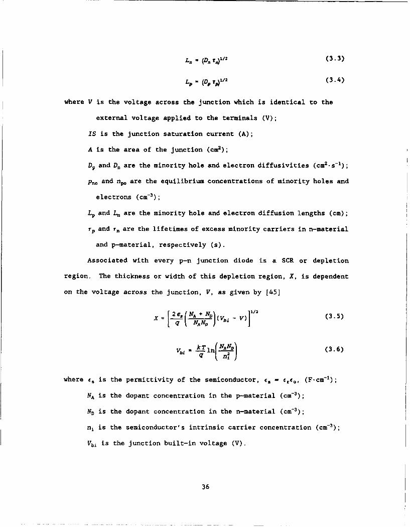
L* - (D., rn)1/2 (3.3)
LP _ (D, r,)1/2 (3.4)
where V is the voltage across the junction which is identical to the
external voltage applied to the terminals (V);
IS is the junction saturation current (A);
A is the area of the junction (cm2);
Dp and D, are the minority hole and electron diffusivities (cm2 .s- 1 );
po and npo are the equilibrium concentrations of minority holes and
electrons (cm 3);
LP and k are the minority hole and electron diffusion lengths (cm);
P and rn are the lifetimes of excess minority carriers in n-material
and p-material, respectively (s).
Associated with every p-n junction diode is a SCR or depletion
region. The thickness or width of this depletion region, X, is dependent
on the voltage across the junction, V, as given by [45]
q e NAN, + I bi - V) 1/ (3.5)
q NAD
=b 7. ln(.HAND) (3.6)
where E, is the permittivity of the semiconductor, e. - erEo, (F.cm-1 );
NA is the dopant concentration in the p-material (cm- 3);
ND is the dopant concentration in the n-material (cm- 3 );
n, is the semiconductor's intrinsic carrier concentration (cm- 3 );
Vbi is the junction built-in voltage (V).
36

The exponent of 4 in Eq. (3.5) is unique to abrupt junctions in which the
transition from n-type to p-type semiconductor occurs on the order of
several angstroms. Mathematically, the exponent, also called the junction
grading factor, results from the solution to Poisson's equation [51:761
d2 _ - qNv (3.7)dx2 es
where 0 is the potential function (V);
x is the distance variable (cm).
Linear or exponential grading of the junction (i.e., the dopant
concentrations are functions of X) will result in exponents as low as h.
The junction grading factors are process parameters which may be defined
in SPICE. The precise growth controls available with MBE allow for very
abrupt junctions. Junctions created by Metal Organic Chemical Vapor
Deposition (MOCVD) are unintentionally graded over approximately 100 -
200 A due to the less precise layer thickness control.
In the case of an HBT, Eqs. (3.5) and (3.6) would be valid only for
the base-collector homojunction. Because all practical HBTs have an
emitter-base heterojunction, the emitter and base have different
permittivities, eE and CB. The E and B subscripts signify emitter and base
respectively in the following expressions for heterojunction depletion
widths on the emitter and base sides of the junction [23:873]:
[ 2e,e, N(Vbi - V~e - 1.64VT) /2 (3.8)
BN, (exN, . e& N,)
-NEx (3.9)NB
37

where VIE is the voltage applied to the base relative to the emitter
(assuming an Npn transistor), NB and NE are the base and emitter dopant
concentrations respectively, VT is the thermal voltage given by kT/q and
1.64 is an empirically derived factor. The expression for determining the
built-in voltage of a heterojunction is given by [52]:
V,=ln s)- - AR (N (3.10)
( n1,,n1) 2Nz
where niE is the intrinsic carrier concentration of the wide-gap emitter;
niB is the intrinsic carrier concentration of the base;
AEc is the conduction band energy difference between the emitter and
the base;
AE is the bandgap difference between the emitter and the base;
Nc and NcB are the conduction band density of states in the emitter
and the base, respectively;
Nv and Nv are the valence band density of states in the emitter
and the base, respectively.
Equation (3.10) reduces to Eq. (3.6) when both the emitter and base have
the same energy bandgap.
Figure 3.1 shows the band diagrams for a homojunction and a
heterojunction at equilibrium. The homojunction is typical for the
emitter-base junction of a Si BJT where the emitter is doped more heavily
than the base; thus, there is more depletion region and band-bending in
the base. The heterojunction diagram is drawn to scale for an abrupt
Al0 . 35Ga0 . 6 As/GaAs emitter-base junction. In this case, most of the band-
bending occurs in the emitter. In both diagrams, the vertical dashed line
represents the metallurgical junction.
38

a) -! x*i
-yp-typeS~Base
n-typeEmitter
X = XI + XO
XE
vbi
Vi8Vbi
p-type
n-type •Emitter !Xe
X :XE + X8 /
Vbi VbiE + VbiO/
Figure 3.1 Homojunction (a) and heterojunction (b) band diagrams atequilibrium.
39

While the junction is reverse-biased, minority carrier drift current
is the dominant transport mechanism across the depletion region.
Therefore, under zero-bias and reverse-bias the region can then be
considered a dielectric void of charge, which can be modeled by a
capacitance. This depletion capacitance is described by the following
expressions for a homojunction and a heterojunction, respectively,
C .A (3.11)
= es es A (3.12)es -ex0 + CB X,
Notice that the heterojunction expression reduces to that of the
homojunction when CE -C.
While the junction is forward-biased, relatively large numbers of
majority carriers diffuse across the junction and become excess minority
carriers. The excess minority carriers are stored within the neutral
regions before recombining, or in the case of the base, before diffusing
across the thin base into the collector. This charge storage effect can
be modeled by a diffusion capacitance as given by [14:96]:
C A(qLp,p + qL n'fp(313-V 2 2 (3.13)
The simplicity of the basic Ebers-Moll model can be traded-off for
more accuracy by including a depletion and diffusion capacitor for each
junction. The resulting equivalent circuit is shown in Fig. 3.2. 1, and
12 have the form of Eq. (3.1) and represent the currents through the base-
collector and base-emitter junctions. CJ, and Cd. are the base-emitter
depletion and diffusion capacitances, whereas CJ1 and CdC are the base-
collector depletion and diffusion capacitances. The model's current
40

source is defined by IZ -Icc - , where Icc and ZIc were given in
Eqs. (2.3) and (2.4) such that
uC 'a exS Ya N'r1C) (3.14)
Physically, IZ is the net current from collector to emitter through the
transistor. Looking at Fig. 2.1, one can see that I• is the current
across the base-emitter junction due to V,, and I• is the current across
the base-collector junction due to VU. In other words, each junction acts
as a voltage controlled current source with respect to the other junction.
IZc is merely the composite current source from collector to emitter.
Another physical phenomena that is not yet considered by the model
is the voltage drop across the neutral regions. The voltage applied to
the terminals of a transistor is never the voltage seen by the respective
junctions because of series resistances. The emitter, base, and collector
resistances are dependent upon the device geometry, but can generally be
described by four components: contact resistance, bulk resistance,
spreading resistance, and lateral contact resistance. Fig. 3.3 shows the
relationship between the geometry of a rectangular finger HBT, the emitter
resistance, RE, and the three components of base series resistance, R.
The figure is purely for illustrative purposes and is not drawn to scale.
Also, the following resistance equations are derived for a geometry with
two base fingers and two collector contacts. Because such a design is
symmetric about the emitter, only one base contact is shown.
Contact resistance occurs when a current moves normally through a
metal-semiconductor interface without spreading or changing direction in
the semiconductor. The expression for contact resistance is given by [53]
where p, is the specific contact resistance (O-cm2 );
41

C
B a t~Ž.~tc&4~ CT
12 T is TC&
E
Figure 3.2 Ebers-Holl equivalent circuit modified to include Junctioncapacitances.
LS
IC'
Collector Layer
Figure 3.3 Lateral view of an HET shoving emitter resistance, RE, and
the three components of base resistance,R.
42

-71
Uc (3.15)
A is the area of the contact, A - SZLZ (cm2 ).
Bulk resistance occurs when current moves a length, L, normal to the
cross-sectional area, A, of a semiconductor having resistivity, p. and is
given by the classic resistance expression
,.jk - PL(3.16)
A
Spreading resistance occurs when current enters a sheet region
normally and leaves in parallel. Equation (3.17) describes the base
spreading resistance of a rectangular emitter finger having a base finger
on either side (53:205]
RP = E 1 (3.17)
where p is the resistivity of the semiconductor (0-cm);
r is the thickness of the region through which the current
spreads (cm);
SE is the width of the emitter finger (cm);
LE is the length of the emitter finger (cm);
1/3 is the spreading factor;
1/2 is due to the current spreading through half of the emitter
width to get to one base contact.
Lateral contact resistance occurs when a current enters a region
beneath and parallel to the surface of the contact it flows through.
Equations (3.18) and (3.19) describe the lateral contact resistance of a
rectangular contact [53:206]
43

Ric - P,-.ýrcth/• (3.18)
7 . (3.19)
P.
where p, is the sheet resistance of the region beneath the contact (0/0);
Lu is the contact metallization length (cm);
S$ is the contact metallization width (cm);
LT is the contact characteristic length (cm).
The total emitter series resistance, RE, of Fig. 3.3 is the sum of
the contact and bulk resistances calculated from Eqs. (3.15) and (3.16).
The base current is split evenly in half between the two base contacts due
to their symmetry about the emitter. Only one of these paths is shown in
Fig. 3.3; thus, the total base series resistance, RD, resulting from two
identical paths in parallel, is given by
R& = R,, * R lR (3.20)2
Recombination currents, which can be significant in HBTs, are not
accounted for in the basic Ebers-Moll model. These recombination currents
are components of IB, and are primarily the surface, SCR, and neutral base
recombination currents. A composite recombination current, which is
dependent on the junction voltage, can be modeled with a non-ideal diode.
A non-ideal diode is represented analytically by a non-unity emission
coefficient. To accurately model the behavior of the transistor in all
modes of operation, a recombination current diode is needed for each
junction, 13 and I.. The complete large-signal equivalent circuit is shown
in Fig. 3.4, where (211
44

is*B("{R4 (3.21)Ion( RH4 No) -] (3.2)
L5~ f"',/ (3.22)BF "X V"• )' m- 11
1 a rSC e Mc- V,.,T_1 (3.23)
eOX VOI,)-1
VE. and Vrc, are the intrinsic voltages seen by the two junctions. These
intrinsic voltages must be differentiated from the applied voltages VU and
VBc due to the voltage drop across the series (also called parasitic)
resistances. This circuit may be linearized to produce the small-signal
hybrid--* equivalent circuit.
Through circuit analysis, it will be shown that the topology of
Fig. 3.4 is equivalent to the SPICE circuit of Fig. 1.7. The first step
in the transformation to Fig. 1.7 is to add each pair of parallel
capacitors. The composite base-emitter capacitance, Cj,+Cd., becomes CBE.
Similarly, the composite base-collector capacitance, CjC+Cdc, becomes CDC.
The intermediate circuit, redrawn to facilitate topology comparison, is
shown in Fig. 3.5.
As mentioned previously, each diode can be analytically represented
with its respective I-V expression. Composite current sources can be
obtained by combining the diode current equations. The result is the
SPICE large-signal equivalent circuit of Fig. 3.6. Expressions for 1B and
Ic are identical to the equations used by SPICE to calculate the terminal
currents for any given junction voltages. Equations (3.25) and (3.26)
fully characterize the dc large-signal model in SPICE [39].
45

C C
i
VOc Re -11 13 =CJC =-Cdc V6c'
12 14 Cie TCde VA'E
VBERE
E E
Figure 3.4 The complete large-signal equivalent circuit.
It
F13
BC1c3
RE
Figure 3.5 Intermediate circuit in the derivation of the SPICE large-
signal equivalent circuit.
46

C
R1R
Bcac
19= 12 +14 +(I1i+13) SC Ic=c(i+ )
RE
E
Figure 3.6 Complete SPICE large-signal equivalent circuit showingcomponents of IB and Ic.
IC = xsfe VDe - V NR Ve _
.rc, [ NP(N7 SRJJNR.VT') -
- xSC exp(~.~. NC 2] (3.25)
xsf (V,1 5 2~ 1 ( (-YC'&-1 1 d,~IS -' ( oe 1] + zS exp( Vj c 1] +I E Ei
BFL '~NFV)-1 7 BRle NA V?, Lex £A( ?
+ ISC[exp( VX')- 1i (3.26)
Having established the physical basis for the SPICE large-signal BJT
circuit, the required model parameters will be examined. Table 3-1 lists
the SPICE model parameters which must be modified to accurately
characterize an HBT. Semiconductor device physics can be used to
determine values for each parameter excluding the emission coefficients.
Because of their complex dependence on the device material, geometry, and
fabrication process, accurate values for the emission coefficients are
47

Table 3-1
SPICE BJT Model Parameters [39]
Parameter Units Description
BF - Ideal maximum forward current gain, Of.•
BR - Ideal maximum reverse current gain, ORa.
IS A Transport saturation current
ISE A Base-emitter leakage saturation current
ISC A Base-collector leakage saturation current
NF - Forward current emission coefficient
NR - Reverse current emission coefficient
NE - Base-emitter leakage emission coefficient
NC - Base-collector leakage emission coefficient
RE 0 Emitter resistance
RB a Base resistance
RC Q Collector resistance
CJE F Base-emitter zero-bias depletion capacitance
CiC F Base-collector zero-bias depletion capacitance
MJE - Base-emitter junction grading factor
MlC - Base-collector junction grading factor
VWE V Base-emitter built-in potential
VJC V Base-collector built-in potential
TF sec Base forward transit time
TR sec Base reverse transit time
XCJC - Fraction of base-collector depletion capacitanceinternal to base
48
better determined through some form of parameter extraction or curve
fitting.
3.2 Linearization
The large-signal equivalent circuit is designed to model a
transistor in all four modes of operation: cutoff, active, saturation and
inverted. The modes of operation are best described by the polarity of
the voltage that appears across each junction as seen in Fig. 3.7. The
transistor described by Fig. 3.7 is a pnp BJT where rip (Pn) is the minority
electron (hole) concentration in the p (n) regions. The large-signal
model is often called a non-linear model and is primarily used for digital
applications, where the transistor acts like a switch. The "on" and "off"
states correspond to saturation and cutoff modes respectively as
illustrated in Fig. 3.8. VEC is the common-emitter configuration output
voltage. The switching time corresponds to the time required for the
transistor to traverse from one state to the other along the load line.
Switching time is a figure of merit for digital devices and can be defined
as either "turn-on" or "turn-off" time. Increasing excess minority
carrier storage in the base occurs during turn-on, whereas those same
carriers (as well as additional carriers stored while in saturation), are
removed during turn-off as depicted Fig. 3.9. Figure 3.9 demonstrates an
npn transistor operating in the common-base configuration where the base
terminal is common to both the input voltage, VE, and the output voltage,
VcB. The input current pulse I I. The turn-on time, r0, is the time
required for the collector current to reach 90% of its saturated value
(Vcc/RL). The storage time, ri, is the time required for the excess
minority carrier concentration at the collector edge of the base to return
49

vzm
E B C E B Cnp Pa np p P
0 W 0 W
ACTIVE SATURATION
0 VC9
E B C E B C
O w O W
CUTOFF INVERTED
Figure 3.7 Pnp junction transistor modes of operation and associatedminority carrier concentrations [51:122].
SATUATION -- |
ONis PR
0 VEC
(o) (b)
Figure 3.8 (a) Relationship between load line, bias point and modes of
operation and (b) corresponding digital switching circuit [51:139].
50

U~~ ~~~~ M, 7 - -• • ..
'E 'C
-1RL
(a)
IF
IE I
I I I~t
(b)I I
IC CI
IcI=Vcc/RL C
II I~mlT 2 fI 0.1 I 1
0 tL tz t.3 t 4
(c)
Figure 3.9 (a) Common-base circuit configuration, (b) emitter currentpulse and (c) corresponding collector current response illustratingtransistor switching times [14:179].
51

to zero. This is the time for the device to leave saturation and enter
the active mode as the base discharges. Once the active mode is reached,
the base continues to discharge until the device essentially enters cutoff
after time T2, the decay time.
Amplifier applications are best modeled with a small-signal or
linear equivalent circuit where the transistor is operated at a specific
bias point in the active mode. The linear equivalent circuit elements are
part of the non-linear equivalent circuit, because the linear model is
operating at a point on the non-linear curve. Note that any point on the
load line of Fig. 3.8 corresponds to a unique bias point defined by VE,
Ic, and IB.
3.3 Physical Small-Signal Modeling
During the derivation of the SPICE large-signal equivalent circuit,
the diodes were replaced by non-linear current sources. The value of each
current source is dependent on the junction voltage. Because the small-
signal model characterizes the transistor operating at a specific dc bias
point, each diode's current and voltage are approximately constant. Any
device whose voltage and current are constant can be modeled with the
corresponding resistance or inverse of resistance, conductance. This
conductance is a small-signal or dynamic conductance which graphically is
equivalent to the slope of the diode's I-V curve at the bias point.
Mathematically, the conductance parameters are calculated via the partial
derivatives of current with respect to junction voltages [39]:
8.r I (3.27)
Reverse Base Conductance: g, - a-s I vV.come.
52

ars (3.28)Forward Base Conductance: ( 3.28
8Ig (3.29)Output (Collector) Conductance: go I V W cow ..
S.ax, J(3.30)Transconductance: ga- I V-y• ca- .
Both HSPICE and the HP 85150B Microwave and RF Design Systems [42]
software perform the partial differentiation to obtain the four
conductance parameters. An ac analysis in HSPICE provides g., l/g, and
I/g0 given the model parameters of Table 3-1, and the dc operating point.
Most small-signal applications operate in the active region, where the
base-collector junction is reverse-biased. Under reverse-bias the
impedance of CA is much smaller than rp, therefore HSPICE considers r,
negligible. Although the hybrid-r small-signal circuit is electrically
valid for all modes of operation, the HSPICE assumption on r. limits
simulations to the active mode. Recall from Fig. 1.8 that CA is the dc
model's CBC at a specific bias point, and that C, is CBE at a specific bias
point. The hybrid-i small signal circuit is shown in Fig. 3.10.
Impedance can be thought of as a frequency dependent resistance.
The impedance of a capacitor is (wC- 1 , where w is radian frequency and C
is the value of the voltage dependent capacitance. Similarly, the
impedance of an inductor is wL, where L is the value of the current
dependent inductance. Obviously, operating at dc, capacitors are open
circuits and inductors are short circuits. The impedance of an inductor
53

increases linearly with increasing frequency and the impedance of a
capacitor decreases non-linearly with increasing frequency.
At low frequencies, (f : 1 MHz), small-valued capacitors (-10 fF)
and inductors (-10 pH) may still be considered open and short circuits,
respectively. However, at microwave frequencies, (I i 1 GHz), those same
capacitors and inductors become parasitic and degrade transistor
performance. Thus, the microwave small-signal circuit is not only a
linearized version of the large-signal circuit, but must include
parasitics as well. The linearized dc model is referred to as the
intrinsic device. The transistor including the surrounding network of
parasitic inductances and capacitances is referred to as the extrinsic
device.
3.4 S-Parameters
The measurements used to characterize a microwave network are S-
parameters. Each S-parameter is an element of an - x i matrix where I is
the number of network ports. For a single transistor in a common-emitter
configuration there are two ports, so the S-parameter matrix is given by
[54:221]
[_J . S SJ [V:) (3.31)
-- (3.32)Vi Vj,*- 0for k~j
where Vj+ is a voltage waveform incident to port j, and Vj- is the voltage
waveform reflected from port i due to the driving signal at port j. An S-
parameter signal flow graph is shown in Fig. 3.11. The condition in
Eq. (3.32) states that only one port may be driven at a time; all other
54

B CP
R13 F_ Rc
B "J•+ 11(c' ,V- C
RE
! E I
Figure 3.10 The hybrid-ir small-signal equivalent circuit.
+
v, S12•24-V 2
• S,, S22 t•6 -- - - - - - - - - - - - - - - - - - - -
Figure 3.11 Two-port S-parameter flow graph [54:221]
55
incident signals are set to zero. This condition is satisfied simply by
impedance matching. Matching a port to its characteristic impedance
eliminates all reflections back on that port in the form of incident
waves. Equation (3.33) defines the reflection coefficient of a
transmission line in terms of its characteristic (Z.) and load (ZL)
impedances.
r = z.-Zo (3.33)ZL Z.
When the load is matched (ZL - zo), r - 0 independent of the length of the
line and the frequency of operation. The accuracy and ease of impedance
matching makes S-parameter measurements ideal for characterizing microwave
devices over wide frequency ranges. The definitions of each of the four
two-port S-parameters are given below [55:278]:
S11 m the input reflection coefficient with the output matched toZo,
S12 - the reverse transmission or feedback coefficient with theinput matched to Z,
S21 - the forward transmission (gain or loss) coefficient with theoutput matched to Z0,
S22 the output reflection coefficient with the input matched toZo.
Because S-parameters are complex, they can be expressed in either
rectangular (a+jb) or polar (IMJ.L) format. Typically, for graphical
analysis, the reflection coefficients $11 and S22 are plotted on a Smith
Chart, while the gains S12 and S21 are plotted on a polar graph.
As mentioned in the literature review, several authors have fit
measured S-parameters to either the hybrid-w or T-model topology to
determine the equivalent circuit element values. To perform such a fit,
one needs to have an idea of what parasitics are physically significant.
56

Parameter extraction via curve-fitting, if the solution converges, will
always determine element values which will produce the measured S-
parameters. However, obtaining a physics-based small-signal model should
be possible by estimating parasitic element values from the device
materials, geometry, and fabrication process.
57

4. Methodology
The initial objective of this thesis effort was to develop a large-
signal model of an HBT that would accurately predict the device's
performance over its range of operation. As previously stated, this model
is a physical model whose parameters are directly related to the device
material, geometry, and fabrication process. Furthermore, this model was
implemented in the readily available SPICE package. The obvious merits of
such a model are its physical nature, its ease of use and straightforward
derivation.
Given the large-signal equivalent circuit topology of Fig. 3.6, the
first step was to calculate physics-based values for each of the
corresponding model parameters of Table 3.1. Physical constants and
equations that provided accurate values for each of the SPICE model
parameters were researched. Knowledge of the device geometry was obtained
from portions of the mask layout. Knowledge of the process was obtained
from the wafer doping profile as well as through discussions with WL/ELRD.
A detailed methodology on each area: material, geometry, and fabrication
process follows.
4.1 Knowledge of Device Material
Throughout the model derivation several general constants were used
which are shown in Table 4-1. Note again that the model does not consider
thermal effects as T is constant at 300 K. The devices modeled were
fabricated with an AlxGa 1_xAs wide-gap emitter, a GaAs base and a GaAs
collector. X is a variable which represents the mole fraction of aluminum
within the ternary III-V compound, AlGal-,As. The compound is a direct-
58

Table 4-1
General Constants Used in Calculations
Parameter Units Description
k- 8.61738 x 10- eV.K- Boltzmann's constant
q - 1.602 x 10-'9 C Electron Charge
to 8.854 x 10⁻¹ F ~cm- Permittivity in vacuum
-o 41r 10-9 H ~cn-' Permeability in vacuum
mo - 9.1095 x 10⁻³¹ Kg Electron rest mass
T - 300 K Absolute temperature
bandgap semiconductor in the range 0 _5 x :s 0.45. Consequently, HBTs are
fabricated with x < 0.45 to avoid the phonon interaction associated with
carrier generation-recombination in indirect-bandgap semiconductors. A
typical value of x is 0.30; the value of x for each of the devices modeled
is 0.35. The most significant effect of the Al is increasing the bandgap
energy. Both the Al.Ga 1jAs bandgap energy and permittivity are linear
functions of x.
Because the Ga~s base is so heavily doped, bandgap narrowing becomes
significant. For example, at NA - 1 x 10¹⁶ the narrowing is only 3.5 meV,
while at NA - 5 x 10¹⁹ the narrowing is 59 meV, which represents a 4.1%
reduction in the GaAs intrinsic bandgap of 1.424 eV. As a result of this
narrowing, the intrinsic carrier concentration in the base increases by a
factor of three.
There are two other materials which play an important role in the
model derivation: gold and polyimide. Gold is the metal used for the
contacts and interconnects. Polyimide is the dielectric used to separate
layers of metal on the wafer since GaAs does not have a stable native
59
oxide as does Si. Table 4.2 summarizes the material parameters and
related expressions.
Another material parameter critical to model derivation is minority
carrier mobility. Mobility is simply a proportionality constant relating
carrier velocity to electric field. Physically, mobility is related to
the mean time between collisions for a carrier, and is therefore affected
by lattice and impurity scattering mechanisms [51]. Empirical expressions
for electron and hole mobility in GaAs have been determined in the
literature [53,56,571. The fit for both carriers has the form of a
Caughey-Thomas equation given by [581:
S = Pmx~ -Pan + Pain(41
+(N (4&
where pa, and Ajn are maximum and minimum values of mobility for each type
of carrier; Nrf and a are curve-fit constants. Table 4-3 lists mobility
parameter values for both electrons and holes in GaAs. Given an impurity
density of N, the mobility of electrons in p-type GaAs is assumed the same
as the mobility of electrons in n-type GaAs [56].
Diffusivity is a material parameter that is a function of mobility
and the Fermi-Dirac integrals [14:29]:
D. =P 1 0.35355 -9 .9x 10-3 ) + 4.45x 0-(4.2)
AT-) C NCNC)
D= pp1 1O.35355(.) 9 . 9 X10⁻³(_)2 + 4.45 x10⁴(.._) (4.3)
where n and p are the electron and hole concentrations (cm- 3 );
Nc is the effective density of states in the conduction band (cm- 3 );
60

Table 4-2(a)
Material Parameters and Expressions Used in Calculations
Expression Units Description
ESG. - 1.424 eV Bandgap energy of intrinsicGaAs
CB - 4. 7 x 1017 cm-3 Conduction band density of_4.x__- states in the GaAs base [14]
S- 7. 0 x 1018 C Valence band density of statesin the GaAs base [14]
NcE - 2.5 x 10¹⁹. cm 3 Conduction band density of(0.6 +states in the AlGaAs emitter
(0.067 + 0.083x) 3 /2 for 0 _5 x _< 0.45 [48]
Nc1 - 2.5 x 10¹⁹. Valence band density of states
"2.5 + cm 3 in the AlGaAs emitter for(0.48 + 0.31x) 31 2 0 5 x 5 0.45 [48]
-1. 79 x 10 cm 3 Intrinsic carrier concentration
iGAs - 7c of GaAs
-1.6 x 10 8(NB)/ 3 eV Bandgap narrowing in the GaAsA~sB 1. x 1-8(B~z/ eV base [56]
Intrinsic carrier concentrationn.(,l/AEga ' 1 /2 in the GaAs base as a function
n•= n''.exp 9-kT) cn- 3 of doping [56]
EgE - ESG.As + 1 247x eV Bandgap energy of the AlGaAs
E•E emitter for 0 < x S 0.45 [59]
EzB - EgG.As - &EgB eV Bandgap energy of the GaAs base
Bandgap difference between theAE - EgE - EgB eV emitter and base at the abrupt
emitter-base heterojunction
/iEc - 0.797x eV Difference in conduction bandenergy between emitter and base
S1/2 Intrinsic carrier concentrationniE = niBexp( 1--m in the AlGaAs emitter [24]
cm 3
61

Table 4-2(b)
Material Parameters and Expressions Used in Calculations
Expression Units Description
eGa. - 13.18 - Relative permittivity of GaAs
Relative permittivity of the'AIGaAs - (GaA - 3.12x - AlGaAs emitter for 0 :5 x :s 0.45
CE- "A2.GaAso F-cm-l Permittivity of the emitter
CB - .&aAsco F-cm-1 Permittivity of the base
Cp -3.5co F-cm- 1 Permittivity of polyimide
Vs.t -1 X 107 cm s_1 Electron saturation velocity inGaAs at 300 K
PA, - 2.44 x 10⁻⁶ 0*cm Resistivity of goldmetallization at 10 GHz [601
so- 1 X 10⁶ cms 1 Surface recombination velocityfor AlGaAs [32]
L- 1 X 105 cm Surface diffusion length forAlGaAs
Table 4-3
Mobility Parameter Values for GaAs [53,56]
Parameter Units Electrons Holes
Amax cm2 . V-I. s-1 8000 400
/min cm2 . V-1 .s- 943 40
Nref cm- 3 2.84 x 10¹⁶ 2.5 x 10¹⁷
a 0.753 0.417
62

Nv is the effective density of states in the valence band (cm- 3 ).
The factor in brackets is the first four terms of the Fermi-Dirac integral
expansion. For nondegenerate semiconductors, the carrier concentration is
typically much less than the corresponding density of states. In this
case, the term in the brackets is essentially unity and the resulting
expression for diffusivity as a function of mobility is called the
Einstein relationship. Note that diffusivity has the units of cm2 -s- 1 , so
q may be omitted if k has the units eV-K-1 as in Table 4-1. As seen in
Eqs. (3.2)-(3.4), diffusivity is needed to calculate saturation currents
and diffusion lengths.
Mobility can also be used to calculate the resistivity, p (0.cm), of
a semiconductor [51:36]:
n =(4.4)- qNDI.n
1 (4.5)PP-= qNA Pp
Currently, very little is known about mobility in AlGa1 _1 As, which
is a function of not only the impurity concentration but also of x.
However, since no empirical curve-fit expressions could be found in the
literature, carrier mobility in the emitter was estimated using the
expressions for GaAs.
4.2 Knowledge of Device Geometry
The most common microwave transistor geometry is interdigitated
where the emitter and base metallization fingers are interdigitated and
the emitters are rectangular stripes. The HBTs modeled in this effort are
unique because they have emitter dots rather than stripes. Consequently,
63
the expressions for calculating the three components of base resistance
(Eqs. 3.16-3.19) had to be reconsidered for cylindrical geometry.
Figure 4.1 shows the layout of one of the MBTs. In particular, the layout
is a 3 micron emitter dot, 5 dot, 1 finger (3u5dlf) device. Actually, the
emitter dots are approximately cylinders sitting on a base finger. This
can be seen in Fig. 4.2 which is a side view cut along AB, where: w,1 is
the width of the collector contact, db is the vertical distance between
the base and emitter metallizations, sbc is the lateral spacing between the
base and collector contacts, and dc is the vertical distance between the
emitter bridge and the collector contact. The emitter-base dot dimensions
for a general emitter diameter are shown in Fig. 4.3. This figure will be
instrumental in calculating the base resistance.
Two geometry dependent parameters used to calculate several SPICE
model parameter values are the base-emitter junction area, Abe, and the
base-collector junction area, Abc. The expressions for each area are
clearly derived from Fig. 4.3 and given by:
Ab = NdcNfi. - 0.i X 10-x (4.6)
A• = NdNt1i(Il + 2 x 10-')(21.) (4.7)
where Ndot is the number of emitter dots per base finger;
Nfin is the number of base fingers;
l,* is the diameter of each emitter dot, I., m 2a 2 (cm).
Notice that the radius of an emitter dot, a 2 , (e.g. 3 microns) is not the
radius of the base-emitter junction, a,. Due to fabrication and
lithography considerations, a2 - a, is the contact spacing between the base
and emitter contacts which is 0.1 microns for all the devices modeled.
64
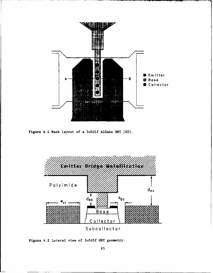
Subcollecctor
Figure 4.2 Laterlalyvie of a3u~dlf AIasHBTgemTry60.
Polyimid65

4.3 Knovledge of the Fabrication Process
The first step in fabricating HBTs is to grow epitaxial layers onto
a GaAs wafer. The layer doping profiles were designed by WL/ELR and grown
by its supplier of epi-material, Epitronics. The doping profile in
Table 4-4 shows the layer structure for one of the three devices modeled.
The other two devices were fabricated to Table 4-4 with the following
exceptions: the 3uldlf device has a collector doping concentration of
2 x 101r cm-3 ; the 2u6d2f device has a collector doping concentration of
1 x 10¹⁷ cM- 3 and a collector thickness of 3.5 x 10⁻⁵ cm. The intrinsic
AlGaAs buffer layer between the GaAs substrate and the GaAs subcollector
serves primarily to minimize substrate leakage. The p-type base dopant is
carbon.
Each of the devices modeled was fabricated via MOCVD so the base-
emitter junction was unintentionally graded over approximately 150 A or
1.5 x 10⁻⁶ cm. Assuming that this graded region is fully within the
emitter, the conduction band spike of Fig. 3.1(b) is almost completely
eliminated. The resulting metallurgical base-emitter junction can be
treated as a homojunction where carrier flow is assumed to be by drift-
diffusion. The presence of a spike causes thermionic emission of carriers
and changes the standard pn products at the SCR boundaries [23,24,62).
Because the Al 0 .3 5Ga0 .5As emitter still exists beyond the grading, the
effective bandgap difference, AE, calculated from Table 4-2 remains
unchanged.
Another parameter that is dependent upon both the material and
fabrication process is the specific contact resistance, p,. For the
devices fabricated by WL/ELR, there is a different p, value for contacts
to n-type and p-type semiconductors: p9c _ 1 x 10⁻⁶ O.cm2 and
66
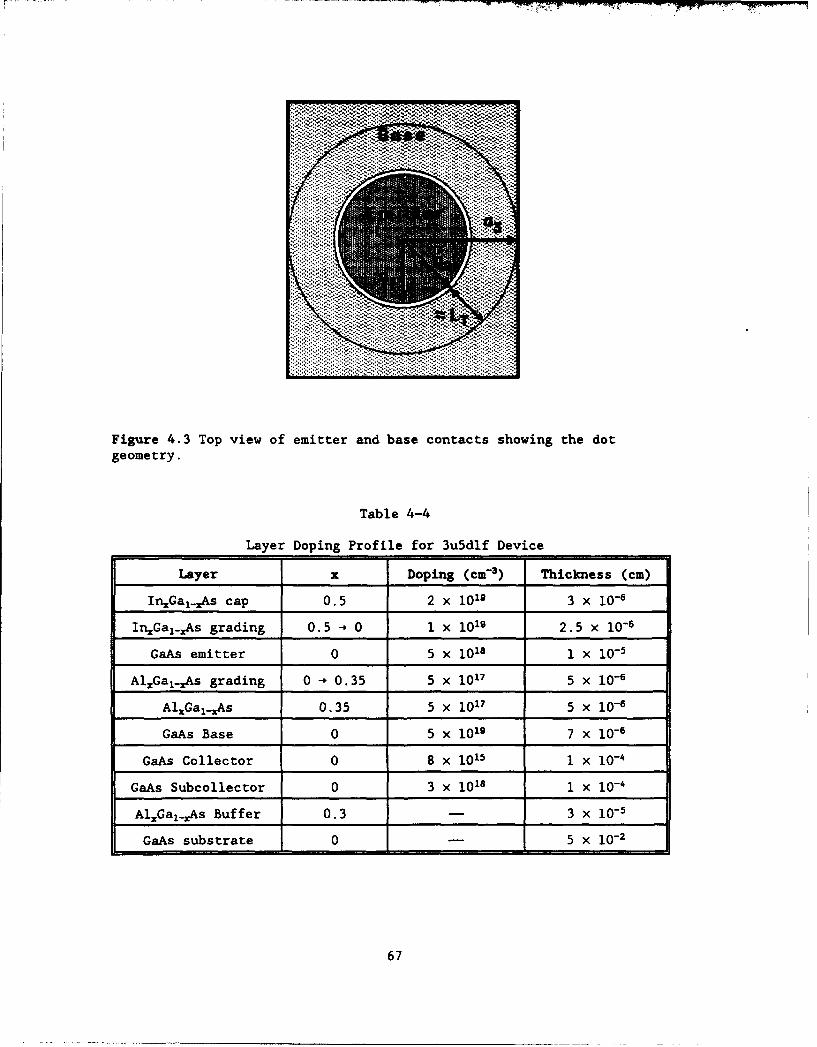
*-..-ZZ
Figure 4.3 Top view of emi.tter and base contacts showing the dotgeometry.
Table 4-4
Layer Doping Profile for 3u5dlf Device
Layer x Doping (cm-3) Thickness (cm)
In1 Gal-,As cap 0. 5 2 x 10¹⁹ 3 x 10⁻⁶
InGa1 -,As grading 0.5 -* 0 1 x 10¹⁹ 2. 5 X 10⁻⁶
GaAs emitter 0 5 x 10¹⁸ 1 x 10⁻⁵
Al 1 Gaj1 xAs grading 0 -~ 0.35 5 x 10¹⁷ 5 x 10⁻⁶
AIGls0.35 5 x101 7 5 x10⁻⁶
GsBae0 5x 10 19 7 x10⁻⁶
GaAs Collector 0 8 X 10¹⁵ 1 x 10O4
GaAs Subcollector 0 3 x 10¹⁸ 1 x 10⁻⁴
Al.Gai-,,As Buf fer 0.A 3 X 10⁻⁵
GaAs substrate 0 -5 X 10⁻²
67

PCP - 5 X 10⁻⁶ 0.cm 2 . Au was used to contact the emitter semiconductor,
Au/Ge/Ni was used to contact the collector, and Ti/Pt/Au was used to
contact the base semiconductor.
After determining the device's physical characteristics solely from
its material, geometry and fabrication process, SPICE model parameters
must be calculated to accurately predict the device's electrical
characteristics. The following section describes the methods used to
calculate each of the SPICE parameters of Table 3-1. These calculated
parameters are not unique to SPICE and may be programmed in any device or
circuit simulator that recognizes the Ebers-Moll or Gummel-Poon junction
trensistor equivalent circuit topology.
4.4 Determination of SPICE Model Parameters
A Mathcad 3.1 [38] program written to calculate all of the SPICE
model parameters is included in Appendix A. This section will discuss
more of the theory behind the various parameters as well as the methods of
calculation.
4.4.1 Forward base transit time, TF. Physically, TF is the
time required for minority carriers entering the neutral base from the
emitter to diffuse across the base to the base-collector SCR. This
parameter is derived in the literature [45,51,53,63]. However, there are
three expressions for TF which have received widespread use.
The most elementary form assumes: 1) 1E - Ic, 2) WB/Ln s 0.1
[51:117], 3) the excess minority carrier concentration at the collector
edge of the neutral base, npB (WB) - 0 [45:160], and 4) the base region is
uniformly doped (no drift field). The first assumption states that
whatever current diffuses into the base from the emitter must also drift
68

out of the base into the collector. The second and third assumptions
state that the excess carrier concentration is linear with distance, and
that the excess base charge, QB, has a triangular area under the
concentration curve. The resulting expression for TF is given by:
TF -- (4.8)Ic 2 D.8
where WB is the effective base width, i.e., the value shown in Table 4-4
less the portions of depleted base at each junction.
Another derivation is similar to the previous with the exception
that npB'(WB) o 0 [53:208]. Instead, npB'(WB) - n,, the saturated velocity
carrier concentration due to velocity overshoot across the base-collector
SCR. This results in the expression for TF having an additional term as
given by:
TF - + W (4.9)2 D.w v.,
Clearly, the additional term becomes negligible for WB/V..t 4 W12/2D..
The final expression for TF is derived mainly in the context of
microwave transistors. The difference is due to a phase shift forced upon
the carriers as they diffuse across the base. The base transport factor,
*, includes an imaginary term at microwave frequencies [63:1167]:
° = sech[(_!ýB) + jJ1/2 (4.10)
Setting • equal to its -3 dB value one obtains:
TF = ,, (4.11)2.43D,,
69

Note that the factor of 2.43 is for a transistor with no drift field in
the base, that is, all current across the base is via diffusion [64,65].
One can readily see that the factor of 2.43 will increase as a base drift
field is introduced since carriers will drift as well as diffuse across
the base, thus reducing TF. Interestingly, Hooke also states that using
a cosh to represent P* will result in a factor of 2 instead of 2.43 for a
uniformly doped base.
4.4.2 Maxi-uu forward connon-enitter current gain, BF.
Sis defined mathematically by [51:127]:
A p IC _ aF (4.12)AIS 1 - a,
'C R C. (4.13)
where I1n is the current due to only electrons from the base into the
collector. Therefore, aF, the common-base current gain, is the percentage
of total emitter current that makes it through the base after
recombination.
Generally, transistors are designed with an emitter efficiency, 7,
very close to unity. Assuming this to be the case for simplicity, the
following expression for P results [51:128]:
n-2L, 2 (4.14)P Wo2
If Eq. (4.8) is chosen as the correct expression for TF, then Eq. (4.14)
may be restated in another widely accepted form.
S- no (4.15)TF
70

where r., is the minority electron lifetime in the base. Both of these
expressions for 6 are approximations because they assume that the only
significant source of base current is bulk base recombination [53:209].
In fact, Eqs. (4.14) and (4.15) overestimate P by as much as an order of
magnitude. However, neither expression accounts for the increased
emitter efficiency resulting from the base-emitter heterojunction bandgap
difference.
In Si BJTs, the emitter is doped much more heavily than the base to
improve efficiency (See Fig. 1.2). This ensures that a few orders of
magnitude more electrons enter the base from the emitter than holes enter
the emitter from the base. Device designers of HBTs are not constrained
to dope the base less than the emitter to achieve this same objective. As
can be shown from Kroemer's wide-gap emitter theory [17], the base of an
HBT may be doped two or three orders of magnitude more heavily than the
emitter. This has a tremendous impact on device performance, primarily in
decreasing parasitic base resistance, RB, increasing the unity current
gain cutoff frequency, fT, and increasing the maximum frequency of
oscillation, fma..
Although W. Shockley first conceptualized the HBT [19), H. Kroemer
can be considered the father of the HBT for his early theoretical
papers [17,18]. An Npn HBT band diagram with associated currents is shown
in Fig. 4.4 where:
Ir is the electron current lost to bulk recombination;
Is is the electron current lost to SCR recombination;
IP is the hole current injected from the base into the emitter;
In is the electron current injected from the emitter into the base.
The following derivation for fl. of an HBT is taken from Kroemer [17]:
71

÷is
+~ j-B
0 1
'p
Figure 4.4 Energy bandgap diagram of a forward-biased Npn A1GaAs/GaAsHBT showing current components. [17:15].
=I _ I' -I , <I L- (4.16)
where P.. is the current gain assuming all recombination currents go to
zero. Equations (3.1) and (3.2) can be used to solve for P :
I qAD.sn., [p - 1] (4.17)
= qADpzP [exp( )V) -i (4.18)
pua I. D ., _•,._ l.no_ (4.19)
IP L., LP, POZ
72

The mass action law definition, expressions for carrier average diffusion
velocity definition, and expressions for intrinsic carrier concentrations
in terms of the effective density of states [51:19] can be substituted
into Eq. (4.19). Equation (4.26) is the resulting expression for 0,_.
n, (4.20)
=n, 2(4.21)- N,
D.D (4.22)
Vp= (4.23)
nix rV T(.4Il = NcNvexp( E9) (.4
2i = c X~~P( -EgN) (4.25)
ni,= ..A.A CN,, e kr
v-, N±, - c v' x Ego (4.26)vpE ND NckNvT
Clearly, for a homojunction device, ES - EB and the exponential factor is
unity. This result shows that Si BJTs must have the emitter doped much
more than the base to achieve a practical P. However, consider an HBT in
which the bandgap difference between the emitter and base is a nominal
200 meV. The corresponding BF will be more than three orders of magnitude
larger than BF for the Si BJT given the same base and emitter dopings.
Because AlGaAs/GaAs HBTs suffer more from parasitic base recombination
currents than do Si BJTs, practical current gains do not share the same
73

wide margin over BJTs. Nevertheless, the example shows the control that
the bandgap difference has on the maximum common-emitter current gain.
4.4.3 Minority carrier lifetime in the base, 7.. Although
T.o is not a SPICE model parameter, it is needed in the calculations of the
model's saturation currents. r.o is the average length of time an excess
minority electron can exist in the p-type base before recombining.
The three main types of recombination in which a minority electron
in p-type GaAs can participate are Shockley-Read-Hall (SRH), radiative and
Auger recombination. An expression for T.o at low-injection is given by
[57:698]:
= (2 . _/_1 ) (4.27)
1 -ovch Ne (4.28)T
SRdf
1 A Ni (4.29)T"Aug
I - B.MN (4.30)
=v d (4.31)
where on is the electron capture cross section (cmz);
vth is the average thermal velocity for an electron, Vth - 1.04 x 10i
cm - ;
nzn is the effective mass of an electron in GaAs, mn - 0.067m.;
Nt is the concentration of recombination centers in the base (cm- 3 );
Ap is the Auger recombination coefficient, Ap - 1 x 10-30 cm6 -s-1;
Bn is the radiative recombination coefficient, Bn - 2 x 10⁻¹⁰ cm3.s-1 .
74

One problem associated with using Eq. (4.28) is the wide range of oa values
reported in the literature [23,51,52). The capture cross section of an
electron should be dependent only on the material, yet differences up to
three orders of magnitude are reported. Additionally, Nt is very process
dependent and can easily change by up to two orders of magnitude. Despite
the fact that further work needs to be done to characterize the lifetime
of excess minority electrons in heavily doped p-type CaAs, the value
provided by Eq. (4.27) is not without merit.
Using liberal values in Eq. (4.28), an - 1 x 10-14 cm2 and
Nt - 1 x 1014 cm-3 [52], the individual recombination lifetimes for the
devices modeled are listed in Table 4-5.
Table 4-5
Calculated Values for Minority Electron Bulk Base Recombination Lifetimes
Component Lifetime (s)
Shockley-Read-Hall 9.623 x 10⁻⁸
Auger 4 x 10⁻¹⁰
Radiative I x 10-10
Total 7.993 x 10⁻¹¹
Clearly, radiative recombination dominates at this base doping density.
The SRH lifetime is nearly three orders of magnitude larger than the
radiative lifetime. Even if the SRH lifetime was reduced by two orders of
magnitude, in an attempt to account for worst case a, and Nt values, the
total lifetime, 7no, would still be dominated by radiative recombination
at a value of 7.386 x 10⁻¹¹ s. Thus, such a large change in non-dominating
SRH lifetime reduces the total lifetime by only 7.6%.
75

Assuming that the value of Tn. listed in Table 4-5 is accurate, a
physical value of BF may be estimated by substituting Eq. (3.3) into
Eq. (4.14). As expected, the resulting BF was two to three times the
value determined from measured I-V data. The explanation, given earlier,
is that Eq. (4.14) only considers bulk base recombination. Empirical fF
clearly depends on surface, emitter-base SCR, and heterointerface
recombination (in abrupt HBTs) currents as well. Each of these other
parasitic components will serve to reduce the value of BF calculated by
Eq. (4.14) closer to the empirical value. The value of BF used in the
SPICE BJT model card is neither a theoretical maximum, nor an empirical
value, but rather the P due only to bulk base recombination [25].
Having accepted Eq. (4.27) to calculate r.m, the excess minority hole
lifetime in the collector, i,, needs to be determined. Because the
collector is doped much less than the base, ro is expected to be much
longer than Tn. The literature has minimal research on lifetimes of holes
in n-type GaAs. Lundstrom et al. [57:700] show that 0 = 20 ns for
ND 5 1 x 1018 cm- 3 . Since the highest value of collector doping, Nc, in the
devices modeled is 1 x 1017 cm- 3, T - 20 ns was used in the calculations.
The diffusivity values determined from Eqs. (4.2) and (4.3), along
with the values of rno and r•, can be substituted into Eqs. (3.3) and
(3.4) to obtain minority carrier diffusion lengths, LnB and Lpc. The
diffusion length is a characteristic length defining the distance minority
carriers must diffuse into a semiconductor to have a density of e-l or
approximately 37% of their junction density. The exponential decay is
obviously due to recombination. The diffusion length (cm) of minority
holes in the AlGaAs emitter, LpE, is calculated from the empirical
expression [23:876]:
76

42.46 - logN5 (4.32)9.21 x 101
4.4.4 Leakage saturation currents, ISE and ISC. Because
the two leakage saturation currents are really the recombination
saturation currents associated with the recombination diodes 13 and 14,
they cannot be calculated from Eq. (3.2). Equation (3.2) is a junction
saturation current that characterizes the ideal drift-diffusion transport
of carriers. Each component of recombination current in a junction
transistor results from some type of trap or state that facilitates the
capture or emission of carriers. An expression for each component
invariably comes from the following integral [66]
I. a qAX2Udx (4.33)xLl
where U is the recombination rate (cm- 3 .s-1 );
x, and X2 are the boundaries between which recombination is expected
to occur (cm).
Recall from the literature review that Ryum and Abdel-Motaleb [23] and
Parikh and Lindholm [24] derived expressions for HBT terminal currents
including all pertinent recombination components. Although these models
are not immediately implemented in any commercial circuit simulator such
as SPICE, they can be adapted to fit the SPICE expressions for IB and Ic
seen in Eqs. (3.25) and (3.26).
SPICE combines the effects of all recombination currents into two
diodes, one for each junction. ISE is the composite recombination
saturation current for leakage dependent on VBE, while ISC is the
saturation current for leakage dependent on VBC,. Thus, ISE and ISC are
77

simply the sums of the individual recombination saturation currents. The
components considered in the devices modeled were neutral base, both SCR,
and base-emitter surface recombination currents. Heterointerface
recombination was not considered, since with a graded emitter the
metallurgical junction is GaAs/GaAs and the number of interface states is
negligible. Expressions for each component may be found in the Mathcad
3.1 file in Appendix A.
4.4.5 Transport saturation current, IS and reverse
parameters, BR and TR. The expression for IS is given by (67]
IS= qAb. ni DO (4.34)WAS5
The base-collector junction saturation current, ICs, is determined by
qA.(nmc + j (4.35)
Next, aR, the reverse common-base current gain was found using the
reciprocity theorem [45]: aR - IS/Ics . a was then used to calculate
the reverse common-emitter current gain, BR, using the form of Eq. (4.12).
One way to conceptualize BR is to swap the emitter and collector, then
follow Kroemer's derivation. The result is a homojunction where the base
is doped two to three orders of magnitude more than the emitter. As
expected from Eq. (4.26), BR < 1. Assuming vr, is the same regardless of
whether the electrons are coming from the emitter or collector, Eq. (4.15)
may now be used to estimate, the reverse base transit time, TR.
4.4.6 Junction grading factors, WJE and MJC. As mentioned
in Section 4.3, each of the HBTs modeled were grown epitaxially via MOCVD.
Despite the unintentional grading of each junction the modeled devices
78
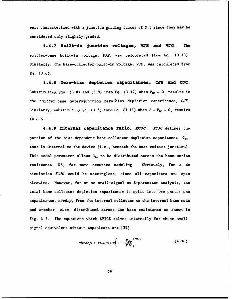
were characterized with a junction grading factor of 0.5 since they may be
considered only slightly graded.
4.4.7 Built-in junction voltages, VJE and VJC. The
emitter-base built-in voltage, VJE, was calculated from Eq. (3.10).
Similarly, the base-collector built-in voltage, VJC, was calculated from
Eq. (3.6).
4.4..8 Zero-bias depletion capacitances, CWE and CJC.
Substituting Eqs. (3.8) and (3.9) into Eq. (3.12) when VIE - 0, results in
the emitter-base heterojunction zero-bias depletion capacitance, CJE.
Similarly, substituti g Eq. (3.5) into Eq. (3.11) when V - VD - 0, results
in CJC.
4.4.9 Internal capacitance ratio, XCJC. XCJC defines the
portion of the bias-dependent base-collector depletion capacitance, Cý,,
that is internal to the device (i.e., beneath the base-emitter junction).
This model parameter allows Cjc to be distributed across the base series
resistance, RB, for more accurate modeling. Obviously, for a dc
simulation XCJC would be meaningless, since all capacitors are open
circuits. However, for an ac small-signal or S-parameter analysis, the
total base-collector depletion capacitance is split into two parts: one
capacitance, cbcdep, from the internal collector to the internal base node
and another, cbcx, distributed across the base resistance as shown in
Fig. 4.5. The equations which SPICE solves internally for these small-
signal equivalent circuit capacitors are 139]
cbcdep = XCJC'CJC(1 - BIC (4.36)
79
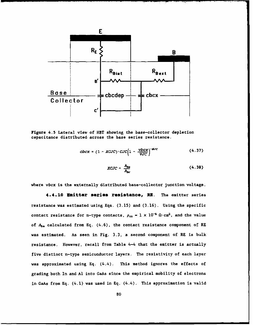
E
I ' --- W;RE R
Bint ext
Ruos e -___ =cbcdep - cbcxCollector
Figure 4.5 Lateral view of HBT showing the base-collector depletioncapacitance distributed across the base series resistance.
cbcx = (1 - XCJC) CJC(1 _ vbcx (4.37)
XCJC - Ab (4.38)Abc
where vbcx is the externally distributed base-collector junction voltage.
4.4.10 Emitter series resistance, RE. The emitter series
resistance was estimated using Eqs. (3.15) and (3.16). Using the specific
contact resistance for n-type contacts, Pc, _ 1 x 10⁻⁶ 0-cm2 , and the value
of Ab. calculated from Eq. (4.6), the contact resistance component of RE
was estimated. As seen in Fig. 3.3, a second component of RE is bulk
resistance. However, recall from Table 4-4 that the emitter is actually
five distinct n-type semiconductor layers. The resistivity of each layer
was approximated using Eq. (4.4). This method ignores the effects of
grading both In and Al into GaAs since the empirical mobility of electrons
in GaAs from Eq. (4.1) was used in Eq. (4.4). This approximation is valid
80

primarily because each of the five layers is relatively thin. Also, a
higher mobility will result in a lower resistivity. Since it is known
that intrinsic In 0 .S3GaOA7As has a mobility approximately 1.6 times
intrinsic GaAs [15:384], one can reasonably assume this method of
determining RE may slightly overestimate the resistivity of the layers
containing In. However, since little to no empirical data exists on the
mobility of AlGaAs, assuming the mobility of AlGaAs is less than the
mobility of GaAs, one can reason that the resistivity of the layers
containing Al is slightly underestimated. As calculated, RE is dominated
by contact resistance, which for the 2u6d2f device was 96.5% of the total
resistance.
4.4.11 Base series resistance, RB. The three components of
RB for a rectangular geometry were shown in Fig. 3.3. and calculated from
Eqs. (3.16) - (3.19). Taking the concepts from Fig. 3.3 and applying them
to the cylindrical geometry of Fig. 4.3, one can see that RB has the same
three components.
R&, is contributed by the disk of base material beneath the emitter
contact. This value is independent of the emitter dot radius and is given
by [68:215]
R=° _ Rgs (4.39)8%
where RBIh is the base region sheet resistance, Rush - P/t (0/D)
Rbu• is due to the thin white annular region in Fig. 4.3 and is
easily shown to be described by
81

= ln(.a) (4.40)
Rje is the resistance due to the radial base current entering the
region beneath the base contact and leaving normal to the contact. The
base contact outer perimeter is rectangular; however, since most of the
current will enter the contact within a radial distance LT of its front
edge [69:392], the base contact can be approximated by an annular region
with inner radius a2 , and outer radius a3 . The expression for lateral
contact resistance in which current enters the inner radius, a2 , of an
annular contact with outer radius a3 , is given by [70]
R.= R,,,L7LTxiLoLT) LT L) (4.41)
= (p.)1 2 (4.42)
where 10 and Ko are zero-order modified Bessel functions of the first and
second kind; 1I and K, are first-order modified Bessel functions of the
first and second kind. Equations (4.39)-(4.42) are valid for a single
emitter dot; therefore, since all dots are in parallel, the total base
resistance is found by dividing the single dot value by the total number
of dots in the device geometry.
4.4.12 Collector series resistance, RC. The collector
current spreads and moves through the subcollector layer in the same way
that the base current moves through the base layer. Consequently, RC has
the same three components as RB including an additional bulk resistance in
the collector layer, Rcb.1k. RCb,,gk is very bias dependent; when the
transistor is operated in the active region, the collector is fully
82

depleted and does not contribute to the series resistance. However, when
the transistor is saturated, almost the entire collector region is
resistive.
Essentially, the only current in the collector region is due to the
electrons that have diffused through the base directly beneath the emitter
contact. Because the emitter dots are relatively small, the collector
cross-sectional area can be approximated by a square with side length
equal to the dot diameter, 1I.. This approximation allows RC to be
calculated entirely with rectangular geometry.
4.4.13 Ideality factors, NY, NRI, N, and NC. Ideality
factors or emission coefficients describe the kT-like dependence of
current on junction voltage. Because of the base-collector homojunction,
the reverse ideality factor, NR is assumed to be 1.0. NF describes the
forward drift-diffusion of carriers across the base-emitter junction and
is expected lie between 1.0 and 1.2. The strong influence of base-emitter
SCR and surface recombination, which have a 2kT-like dependence, cause NE
to be close to 2.0. Similarly, NC is expected to lie between 1.5 and 2.0.
The ideality factors are the only model parameters that have an
exponential effect on model data. Even a third decimal place deviation in
NE or NF can produce a noticeable change in the I-V characteristics so a
good guess value is usually inadequate for good agreement. For this
reason each of the three unknown ideality factors was curve fit to
measured data using HSPICE optimization.
4.4.14 Corner for high current PF degradation, IKF. This
model parameter is used to characterize the degradation of OF at high
collector currents. An approximate expression for IKF is given by
83

i•. . qAb, Ncvmc (4.43)
This expression identifies the critical (collector) current obtained when
the concentration of carriers crossing the reverse biased base-collector
junction approaches the concentration of mobile charge carriers in the
collector, Nc.
4.5 SPICE do Simulation
While seeking to determine the most accurate values for the SPICE
HBT model parameters, a SPICE testbench was written that would provide a
set of I-V curves. Annotated HSPICE files for the three devices modeled
are included in Appendix B. I-V curves for an npn junction transistor
consist of Ic against VCE for various discrete values of 1B. To obtain
this data the SPICE testbench required a voltage source, Vce, a current
source, Ib, a source resistance, Rsrc, and a BJT element, Ql. The
1 x 10²¹ 0 source resistance was placed in parallel with the current source
to facilitate convergence and to ensure that all of Ib entered the base.
The SPICE dc testbench circuit is shown in Fig. 4.6.
Next, using the SPICE .dc statement, a dc simulation was run using
a nested sweep of both Vce and Ib. Vce was swept with enough resolution
to generate a curve over the range of interest and Ib was incremented to
match the measured data. During the simulation, data was printed to the
screen using the .print dc statement. Columns of data for Vce, Vbe, Ib,
and Ic were saved to an ASCII data file. The initial simulations used
model parameter data consolidated from Rockwell [71:33] and TRW [26:2126]
HBTs. These parameters were replaced as physics-based values of the
parameters that described WL/ELR's HBTs were calculated. Throughout the
model derivation process, interim model data was compared to measured
84

data. Differences between the two were noted and sensitivity analyses
were run to determine which SPICE model parameters had the largest impact
on minimizing the difference. Often, manual curve-fit values were
obtained via trial-and-error. Once good agreement was obtained, the
curve-fit parameters were examined to see if there was possibly a physical
basis to substantiate the new value. Several iterations of the Mathcad
program were required to develop physics-based parameter values that
provided consistently good agreement for all three devices modeled.
4.6 SPICE ac Simulation
The first step in a SPICE ac analysis is to provide a dc bias to the
HBT element. This is done by choosing specific values for Vce and Ib in
the active region corresponding to the bias points of measured S-
parameters. Network ports then need to be defined using the .net
statement whose syntax is (401
.net output input RFOT - val2 JUN - vall
where Input is the ac input voltage or current source name;
output is the output port defined by a voltage between two nodes, an
output current, or element current;
FUT is the output or load resistance with value val2;
RIN is the input or source resistance with value vall.
In the common-emitter configuration, the input port may be defined by Ib,
and the output port by i(Vce), the output collector current, as shown in
Fig. 4.7. Given both ports defined by currents, HSPICE initially
calculates the H matrix and converts the h-parameters to whatever metric
is desired: z-, y-, g-, or s-parameters.
85

B +lb E, -Vce
Figure 4.6 SPICE junction transistor dc testbench.
C 4--i(Vce)
Port I lb R~src -EVe Pr
0.
Figure 4.7 SPICE junction transistor ac testbench.
86

The .ac statement performs the ac analysis and has many options.
For the purpose of this model, a 50 point linear sweep of frequency from
1 GHz to 50 GHz was conducted. HSPICE linearizes the dc circuit of
Fig. 3.6 by solving Eqs. (3.27)-(3.30). The resulting hybrid-i equivalent
circuit is shown in Fig. 4.8. A script of the ac simulation in which all
small-signal element values are calculated may be found in Appendix B.
HSPICE automatically isolates the dc and ac sources during an ac
simulation by shorting all the dc voltage sources and opening all the dc
current sources.
Similar to the dc analysis, using the .print ac statement, data was
printed to the screen and saved to a file. The data saved were the four
S-parameters in polar form (IMI.L). Saving the data in polar form was
necessary to avoid sx.bsequent conversion because the analysis software,
Axum, requires the data in polar form to accurately plot. Since the
measured S-parameters provided by WL/ELR were in rectangular form (a+jb),
they had to be converted to polar form in Axum.
4.7 Adding Parasitics to the Small-signal Equivalent Circuit
An incremental section of transmission line can be represented by a
lumped-element equivalent circuit comprised of a series resistance and
inductance and a shunt conductance and capacitance. Considering the
microwave operation of the HBT, modeling the device with a lumped series
inductor on each terminal is logical. Similarly, a capacitor shunting
each pair of nodes is also common in the literature [31,72,73]. The
resulting small-signal hybrid-i equivalent circuit having three parasitic
capacitors and three parasitic inductors is shown in Fig. 4.9.
87

Cp ex tI i
Re x R it CPl o mt Rc
5 N C
""+ +
'B' E' §w C, g(u 8 Ir " g0
REE 1 e
Figure 4.8 HSPICE hybrid-w small-signal equivalent circuit with base-collector depletion capacitance distributed across the base resistance.
Cbcp
Lb R49t SmRa n Cp alt c uitRc Le p
B R•, RC
ER
Lop
Figure 4.9 Small-signal hybrid-w equivalent circuit complete with
parasitic elements.
88
Most of the geometry variables used in the parasitic calculations
were obtained from a large layout of the device, similar to Fig. 4.1. For
the devices modeled, the width of the base finger is always two microns
wider than the diameter of the emitter dot. Consequently, the width of
the base finger was a convenient metric from which to determine all other
geometry parameters using a ruler appropriately scaled for maximum
accuracy.
Determining where parasitics need to be considered is important when
the device geometry consists of probe pads. The probe pads for each of
the devices modeled are coplanar and were designed for an impedance of
50 0. Thus, the pads themselves do not contribute any parasitic reactance
or susceptance; only the interconnects and contacts need to be considered.
The resistance typically in series with each inductance is the
resistance of the metal interconnects due to the finite resistivity of Au.
At microwave frequencies this resistance may be calculated as [60:146]
R-= pA.L (4.44)3mtW
where PAu has the value shown in Table 4-2;
L is the length of the metal strip in the direction of current (cm);
t is the thickness of the metal strip (cm);
W is the width of the metal strip (cm);
m is the number of identical strip fingers in parallel.
This resistance was found to be up to two orders of magnitude smaller than
the terminal series resistances (RE, RB, and RC) and was therefore
neglected.
The total inductance of any geometry is the sum of its internal and
external inductances [74:246]. The internal inductance per unit length of
89

a wire is simply Lint - p/8ir (H) [74:247], where p is the permeability
of the wire, which for non-magnetic materials is essentially 1A from Table
4-1. When two conductors are nearby each other, as in the case of a
planar transmission line, external inductance typically dominates and may
be approximated by [60:99]
POdL (4.45)L "mW
where d is the separation between the two planar conductors (cm).
Recall the geometry of Figs. 4.1 and 4.2 and consider the parasitic
collector inductance, Lcp. The collector metallization and the emitter
bridge can be approximated as a section of planar transmission line in the
region where they overlap (i.e., beneath the emitter bridge). Using
Eq. (4.45), L,, may be estimated by substituting d.c for d and Wc1 for W.
For the 3u5dlf device, m - 2 since there are two collector fingers. L
is the length of each finger beneath the emitter bridge (or approximately
the width of the bridge).
The parasitic base inductance, Lbp, can be similarly estimated. One
must remember that inductances add in series and look for ways to simplify
the geometry such that Eq. (4.45) may be used. Figure 4.10 represents the
base contact of a single dot. Notice that for each dot the base metal can
be approximated by two strips of width vbb and length 1../2 in series with
the parallel combination of two strips of width 'eb and length 1,,. This
configuration of base metal can be approximated as a section of planar
transmission line separated from the emitter bridge by a distance d.b. LP
can now be easily estimated by calculating the inductance of a single dot,
multiplying this amount by the number of dots per finger and dividing by
the number of base fingers in the geometry.
90

The parasitic emitter inductance, L., can be estimated by the
parallel combination of L,, and L4.. The reason for this is that emitter
is common to both Lp and L. (i.e., the emitter bridge is one of the
planar conductors contributing to L,, and 4..). Therefore, both L,, and 4.
are parallel components of L.p.
The parasitic capacitance can be estimated using the classic
expression for the static capacitance of a parallel plate geometry,
C - eA/d . This formula holds since for A - WL , W >_ L ; d in all
cases for the devices modeled. The same variables used to characterize
the collector inductance can be used to estimate the collector-emitter
parasitic capacitance, Ccep. A is the area of the collector metallization
beneath the emitter bridge, d.c is the distance between the two parallel
plates, and e is the permittivity of polyimide.
Estimating the base-emitter parasitic capacitance, Cbhp, is simpler
than estimating Lp. A is the area of just the base metal which is
approximately Ab, - Ab4. Obviously, d is dab from Fig. 4.2. One can also
notice from Fig. 4.2 that a cylinder of emitter metal connects the bridge
to the emitter semiconductor. The capacitance contribution due to this
emitter post has not been considered. This additional component of Cbep
is expected to cause the actual base-emitter parasitic capacitance to be
at least two times larger than the calculated parallel plate Cbep.
Actually, same emitter trench and posts were not considered in the
estimate of Ccop. Thus, one would expect Ccep to be similarly
underestimated by at least a factor of two. The point is that there are
more parasitic capacitance components than just the simple parallel plate
approximations. Although such contributions are known to exist,
physically calculating these additional contributions is non-trivial.
91

When considering Cbp, the base-collector interelectrode capacitance,
there is no interconnect or pad overlap. This results in a fringing
capacitance. A key expression in calculating this fringing capacitance is
given by [75]:
X = [ (L + L_ - LO)L"0 I (4.46)[(L + L&o)(Lo + L&o)
where the variables are defined in Fig. 4. 11. The complete expression and
variables involved in this interelectrode fringing capacitance are
included in the Mathcad file in Appendix A. The assumption is that both
conductors lie in the same plane. The simplifications of the base metal
shown in Fig. 4.10 are also key to estimating Cbjp. sbc from Fig. 4.2 is
equivalent to Lo for all components of fringing Cbcp. The base-collector
capacitance of a single dot is calculated and multiplied by the total
number of dots in the geometry since capacitors add in parallel.
Logically, one might also contemplate a parasitic resistance
associated with the interconnects. This resistance, in parallel with the
associated parasitic capacitance, would model any current leakage between
the base and collector terminals to ground. Using the classic resistance
formula
pL (4.47)
where p is the resistivity of intrinsic GaAs, p - 1 x 10⁶ 0-cm; L and W are
the same order of magnitude; t is the depth of the leakage current into
the substrate, t 4 1 cm. Clearly then, Rl.,k ) l0 Q.
Model calculated S-parameters were collected at multiple bias points
for each device via HSPICE ac simulations for two different equivalent
circuit configurations: Fig. 4.8 (the bare model without the parasitic
92

lee... .. .... ............. +:.m ........ ............. -......... ee
Wbb
Figure 4.10 Top-view of the simplified base metallization geometry for asingle emitter dot.
K LO LSK +- L
Figure 4.11 Annotated diagram of fringing capacitance between two
conductors lying in the same plane.
93

elements) and Fig. 4.9 (the full model with all six parasitic elements).
Each of these sets of model data were then plotted against the
corresponding measured data.
94
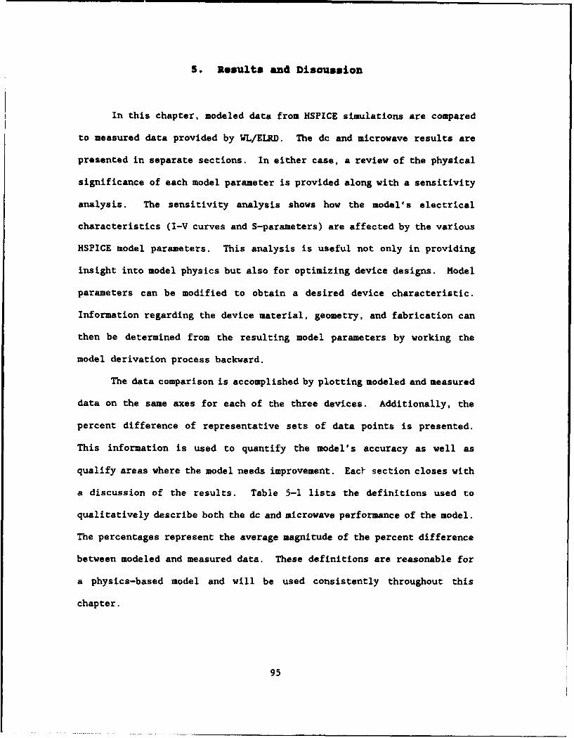
5. Results and Discussion
In this chapter, modeled data from HSPICE simulations are compared
to measured data provided by WL/ELRD. The dc and microwave results are
presented in separate sections. In either case, a review of the physical
significance of each model parameter is provided along with a sensitivity
analysis. The sensitivity analysis shows how the model's electrical
characteristics (I-V curves and S-parameters) are affected by the various
HSPICE model parameters. This analysis is useful not only in providing
insight into model physics but also for optimizing device designs. Model
parameters can be modified to obtain a desired device characteristic.
Information regarding the device material, geometry, and fabrication can
then be determined from the resulting model parameters by working the
model derivation process backward.
The data comparison is accomplished by plotting modeled and measured
data on the same axes for each of the three devices. Additionally, the
percent difference of representative sets of data points is presented.
This information is used to quantify the model's accuracy as well as
qualify areas where the model needs improvement. EacY section closes with
a discussion of the results. Table 5-1 lists the definitions used to
qualitatively describe both the dc and microwave performance of the model.
The percentages represent the average magnitude of the percent difference
between modeled and measured data. These definitions are reasonable for
a physics-based model and will be used consistently throughout this
chapter.
95

Table 5-1
Definitions for Qualitative Model Performance
Average IPercent Differencel Agreement Qualifier
JA%j -< 2.5% Excellent
2.5% < IA%j -s 5% Very Good
5% < 14%i s 15% Good
15% < la%I s 25% Fair
25% s i1%i Poor
5.1 DC Results
The DC steady-state model is fully characterized by Eqs. (3.25) and
(3.26), which are the HSPICE expressions for the collector and base
terminal currents, respectively. For convenience, these equations are
restated here:
qbyNF-vT) NR-VT) BR NR-VT
- xsc exp( c'-v ] (5.1)
S ex( 'W' ] -S- ___ 1 SjepBF .[e~ NF-V2. ] BR NRV .n.v JxEe(NEIvT) ]
+ xscfexp( CV4) _1] (5.2)
The model parameters that affect the dc characteristics are the saturation
currents (IS, ISE, and ISC), the ideality factors (NF, NR, NE, and NC),
the series resistances (RE, RB, and RC), and the common-emitter current
gains (BF and BR). Notice that a factor of qb has been added to the
denominator of the first term in Eq. (5.1). qb results from the Gummel-
Poon model and has a default value of unity in the SPICE BJT model.
96

Although neglected in the dc model derivation of Chapter 3, qb can have a
significant effect on the agreement with measured data. The HSPICE
expressions for qb are
qb (1+ 4qa)1/"] (5.3)
Vve a (5.4)q, VAF VAR)
q2=.JIexd4~!- Vow I + ISCexJ wi' (5.5)
NF1-V. -XR AZRkVr
where VAT and VAR are the forward and reverse early voltages (V);
IKF and IER are the forward and reverse high-level injection,
degradation currents (A).
The early voltages are metrics for base-width modulation where Ic increases
with increasing VcZ. However, since the base of a typical HBT is doped
much more heavily than either the emitter or collector, base-width
modulation is negligible and q, becomes unity. hKF is a para-eter that
characterizes the high current degradation of OF due to the high-level
injection of carriers from the base into the emitter. Because of the high
current densities obtainable with HBTs, base pushout (also called the Kirk
effect), is a common phenomena. The Kirk effect causes the effective base
width to increase, thereby decreasing jBF. The Kirk effect can be modeled
with IKF or included in the four recombination parameters: ISE, ISC, NE,
and NC. The Kirk effect was not significant in the one finger devices and
was modeled with the recombination parameters in the two finger device.
Because common-emitter I-V characteristics were the only dc
measurements obtained on the three devices modeled, only common-emitter
97

I-V characteristic sensitivities to HSPICE model parameters will be
discussed. The additional usefulness of Gunnel plot sensitivities will be
addressed in the next chapter.
The series resistances, though not shown in Eqs (5.1) and (5.2),
directly influence the junction voltages, Vs.r and Vs.c.. Both RE and RC
affect the slope of the I-V curves in saturation. While in saturation, an
increase in RC means a higher VCZ needs to be applied to maintain the same
Ic. The transistor will remain in saturation at higher VcE (a decreased
slope) since more voltage is dropped across a larger resistor, decreasing
the voltage seen by the internal collector node, Vc,. Finally, the active
mode is reached when the base-collector junction becomes reverse biased
(Vc' > V,,).
A similar scenario occurs when RE is increased. Given a constant IB
for each curve, to maintain the same Ic, the potential at VE. must increase
due to the increased voltage drop across RE. Consequently, the input
voltage Vi must increase to maintain the same VBJE. Kirchhoff's voltage
law then demands that the output voltage VcE also increase resulting in a
lower slope through saturation. The slope is more sensitive to changes in
RE and decreases linearly with increasing RC or RE.
RB had no effect on the I-V curves. Since I9 is a constant for each
curve, any change in RB results in a corresponding change in VBE necessary
to maintain the proper VBE, and VBC, relationship. The only effect that
a change in RB had on the terminal characteristics of the simulated model
was a change in VB1 , the applied input voltage. As expected, VSE changed
proportionally with RB.
5.1.1 3u1d4f and 3uSdlf Device do Results. The 3uldlf and
3u5dlf devices have regions of nearly constant current gain as shown in
98

Figs. 5.1 and 5.2. For each device, a linear regression of the top six
empirical data points shows that OF is nearly constant at the value
indicated by the regression line. Using this value of OF in the model card
for BF will produce I-V curves that agree well for all except the lowest
I1 curves. This is because recombination currents, which degrade OF, are
the most noticeable at low bias. ISE, ISC, NE, and NC are necessary to
model any bias dependence of OF, including an HBT's offset voltage bias
dependence. However, because the 3uldlf and 3u5dlf devices have a region
where OF is nearly constant, a more simple model that accounts for
recombination using a constant empirical BF was developed.
The comparison between modeled and measured common-emitter I-V
characteristics for the 3uldlf device is shown in Figs. 5.3 and 5.4. The
model parameters were calculated with the Mathcad 3.1 program in Appendix
A. The HSPICE dc testbench used to generate the modeled data is in
Appendix B. The set of HSPICE BJT dc parameters used to generate the
model data of Figs. 5.3 and 5.4 is shown in Table 5-2.
As mentioned in Chapter 4, NR was assumed to be unity. Although
HSPICE was not used to optimize any model parameters, BR and NF were
manually fit to best match the measured data. First, BR was chosen small
enough to provide very good agreement in the reverse active region. Next,
NF was chosen to best match the two sets of data in the saturation region
and at the offset voltage. For models that account for recombination with
an empirical BF, increasing NF shifts the set of I-V curves to the right,
and decreasing shifts the curves to the left. NR and BR have the reverse
effect on the set of I-V curves. Increasing each of these parameters will
shift the curves to the left. Naturally, the curves are more sensitive to
changes in NF and NR because of the exponential dependence.
99
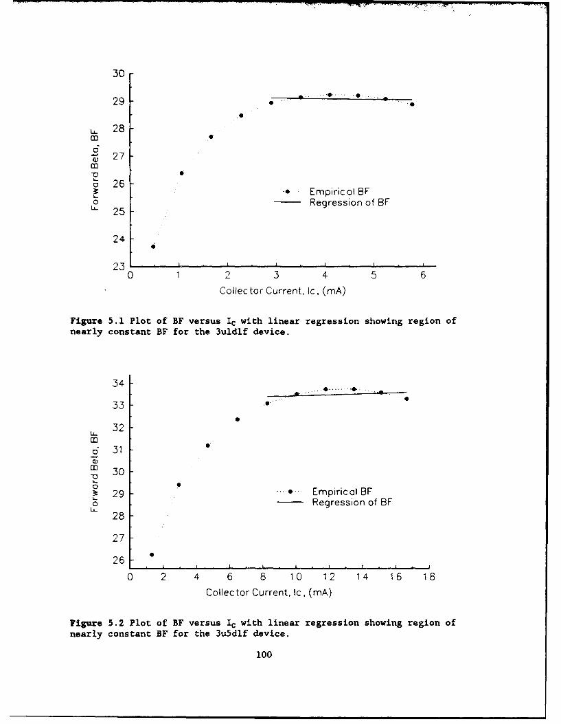
30
2 9 .... .. ..
LL 28Mr500 27M0 26
2: 6.- Empirical BF
0 Regression of BF"~ 25
24
23 , i0 1 2 3 4 5 6
Collec tor Current, Ic, (mA)
Figure 5.1 Plot of BF versus IC with linear regression showing region ofnearly constant BF for the 3uldlf device.
34
33
32M0
o 31
IM 30o 0
1 29 . EmpiricalBF0 Regression of BF
28
27
26 2 6I I , I I I , I I I I
0 2 4 6 8 10 12 14 16 18
Collector Current, Ic, (mA)
Figure 5.2 Plot of BF versus Ic with linear regression showing region of
nearly constant BF for the 3u5dlf device.
100

0 Measured - Modeied
6-. 6200 uA
5
.4 4 ,c
L 3
0 2
20 uA0
-10 1 2 3 4
Collec tor-Emitter voltage, Vc e, (V)
Figure 5.3 I-V characteristics for the 3uldlf device with IB swept in20 pA increments.
0 Measured --- Modeled •
.-- 0.00< 20 uA
Eo -0.05
0•. -0.15
-0.210200 uA
0.0 0.1 0.2 0.3
Collec tor- Emitter voltage, Vc e, (V)
Figure 5.4 Reverse I-V characteristics for the 3uldlf device with IB
swept in 20 pA increments.
101

The specific contact resistance for n-type contacts, pn, was
estimated at 1 x 10⁻⁶ •.cm2 . The actual value is dependent on process
variations and could vary by a factor of two in either direction. The
value used by Mathcad to calculate RE and RC for all three devices modeled
was 2 x 10⁻⁶ Q.cm2 , only because this value tended to provide better
agreement on S21 at the lower frequencies.
The 3uldlf device has very good agreement in the forward and reverse
active regions and good to poor agreement in saturation depending on the
degree of saturation. In saturation, the modeled curves do not quite have
the same variable slope as the measured curves do. This observation may
be related to the bias dependence of RC. Increasing RC has been shown to
decrease the slope of each I-V curve. However, HSPICE does not consider
that the actual value of RC changes with Vac,. To do this, HSPICE would
require information on the doping and thickness of the collector layer.
Instead, HSPICE regards RC as a constant. Thus, the slopes of all the
curves change by the same amount when RC is changed (i.e., independent of
bias). Carrier recombination is another phenomenon that effects the
slopes of the curves in saturation, but only at low bias. If a sufficient
number of data points were recorded, the measured curves for the few
lowest 1B values would show a distinctly lower slope than the corresponding
modeled curves. This is due to recombination hindering a faster rise in
Ic at the lower bias levels. This bias dependence is not modeled by the
constant empirical BF; therefore, the modeled curves have steeper, bias
insensitive slopes.
Another bias dependence not accounted for with the constant
empirical BF is that of the offset voltage. The offset voltage of the
modeled curves increases with increasing bias. The proper relationship
102

has offset voltage inversely proportional to bias [26]. The model's
inability to accurately model the bias dependent offset voltage results in
poor agreement at VCE - 0.3 V for both the 3uldlf and 3u5dlf devices. This
is because the interpolated measured offset voltages occur in the range of
0.285 to 0.3 V. The small collector current magnitudes at VCE - 0.3 V
intensify the percent differences.
The same modeling procedure was performed on the 3u5dlf device and
the resulting model parameters are listed in Table 5-3. The ensuing I-V
characteristics are shown in Figs. 5.5 and 5.6. Because the emitter dot
diameter is the same for both the one dot and five dot devices, RE and RB
for the 3u5dlf device are exactly one fifth of the respective 3uldlf
values. This is because each of the dots are in parallel RC has a more
complex geometry dependence, but is approximately one fifth of the 3uldlf
value for the same reason. The 3u5dlf saturation current is larger than
the value calculated for the 3uldlf device primarily due to the larger
junction areas.
Once again, the effects of device self-heating are readily seen in
the highest four curves at VE 2 3 volts. In fact, the top curve (IU - 500
pA) is effected almost immediately after entering the forward active
region. Like the 3uldlf device, the 3uSdlf device model slightly
overestimates the active region collector current for the lowest four
curves (50 pA : 1S 5 200 #A). This is due to the model having a constant
JF that was chosen to match the near constant empirical 6F of the highest
six curves (250 pA 5 IB 5 500 pA).
Overall, the physics-based models for the 3uldlf and 3uSdlf devices
provide very good agreement with the measured data. Plots of the average
magnitude of the percent difference between modeled and measured data
103

Table 5-2
3uldlf SPICE WJT dc Model Parameters
Parameter Units Value Used in RSPICE BJT Model Card
BF -83.541
BR 0.1512
NF 1.1121
NR 1.0000
ISE A default 0
ISC A default 0
is A 2.2345 x 10⁻²r
RE a 33.6707
RB a 43.2846
RC a 68.713
Table 5-3
3u5dlf SPICE BJT dc Model Parameters
Parameter Units Value Used in HSPICE BJT Model Card
BF - 83.429
BR - 0.0569
NF - 1.1393
NR - 1.0000
ISE A default 0
ISC A default 0
IS A 1.1169 x 10⁻²⁵
RE 6.7341
RB 0 8.6569
RC 0 16.785
104

0 Measured - Modeled
17
< 15E
'- 3 13
0U 11
00
0. 9O8 5
0.
1 0
-1
0 1 23 4
Collec tar- Emitter voltage, Vc e, (Volts)
Figure 5.5 I-V characteristics for the 3u~dlf device with IB swept in50 pA increments.
0.2
•'- 0.1 --- Modeled
S0.0
- ~-0.2 iC
0 -0.2
<,. - 0 .3
S -0.4
-0.5 0
0.0 0.1 0.2 0.3
Coliec, tar-Emitter voltage, Vce. (Volts.')
Figure 5.6 Reverse I-V characteristics for the 3u~dlf device with IB
swept in 50 pA increments.
105

points for each of the devices are shown in Figs. 5.7 and 5.8. Each bar
indicates how far the modeled 1C value (theory) is from the measured value
(actual) at each measured point averaged over all the constant 1B curves.
The cluster of bars on both graphs represents data at VY - 0, 0.05, 0.1,
0.15, and 0.2 V. The data presented quantifies the performance of the
model.
The 3uldlf model overestimates Ic by less than 4% in the reverse
active region, (0, 0.05, and 0.1 V). Good agreement is maintained as the
device leaves the reverse active region and begins to enter saturation
(0.15 and 0.2 V). The approximate 60, 21, and 15% differences (occurring
at 0.3, 0.4, and 0.5 V, respectively) are due to difficulties matching a
variable slope in the saturation region. Thus, inaccuracies in modeling
the bias dependence of RC and recombination result in fair to poor
agreement in the saturation region. The largest difference of 60% at
0.3 V is due to the offset voltage increasing with bias rather than
decreasing with bias as the measured curves do. Even though the offset
voltages for the model and actual device are within the same range of VCE,
the actual and modeled offsets on average do not coincide within the
range.
Very good agreement is obtained in the forward active region (1,
1.5, and 2 V) with a difference of less than 5%. The overestimation at
the two highest VCE values (3 and 4 V) is due to transistor self-heating
which reduces the measured IC values.
The 3u5dlf dc model performs just as well as the 3uldlf model. In
the reverse active region (0, 0.05, and 0.1 V), the model overestimates Ic
an average of less than 5%. When the device begins to enter saturation
(0.15 and 0.2 V), the model maintains good agreement. Similar to the
106

-. 60
o 50C
•.- 40
c 30
• 200UQ) 10
0 1 2 3 4
Collec tor-emitter voltage, Vc e, (V)
Figure 5.7 Magnitude of the percent difference between modeled andmeasured Ic averaged over all ten IB curves.
30
d 25c . - Actuol volue for 0.3 V is
C_ 50 times plotted value.S20
C 15
U I10
00 1 2 3 4
Collector-emitter voltage, Vc e, (V)
Figure 5.8 Magnitude of the percent difference between modeled and
measured Ic averaged over all ten II curves.
107

3uldlf device, inaccuracies in modeling the bias dependence of RC and
recombination result in fair to poor agreement in the saturation region.
Again, the largest difference (an average of 1300%) occurs at 0.3 V.
As discussed earlier, this is due to the bias dependencies of RC and
0,. The bias dependence of RC could be corrected by modifying the SPICE
code to handle a variable RC. The bias dependence of O, can be accounted
for by curve fitting values for ISE, ISC, NE, and NC. However, the same
problem was encountered when fitting values for ISE, ISC, NE, and NC for
the 3uldlf and 3u5dlf devices. The problem is that the HSPICE
optimization routine is too sensitive to the initial values chosen for ISE
and ISC. Several initial values were chosen within an order of magnitude
from the physics-based value calculated by Mathcad. For each optimization
attempt, the modeled data were as much as a factor of two different from
the measured data in the forward active region. The conclusion is that
process variations, which are difficult to account for physically, caused
the actual recombination saturation currents to be significantly different
than the physically calculated values. For this reason, the 3uldlf and
3u5dlf devices were modeled by accounting for recombination with an
empirical OF. Unless the bias dependence of the offset voltage is
accounted for somehow, the average percent difference in Ic will always
result in poor agreement within the range of the offset voltages.
Very good agreement is obtained in the forward active region (1,
1.5, and 2 V) with an average difference of about-5%. As with the 3uldlf
device, the 7% average difference at 3 and 4 V can be attributed to self-
heating.
5.1.2 2u6d2f Device de Results. Figure 5.9 shows the
excellent agreement that can be obtained by neglecting ISE and ISC, and
108

using an empirical P for BF with the 2u6d2f device. Since O is not
constant, an expression for BF as a function of Z9 was determined via
Axum's curve fitting capabilities as shown in Fig. 5.10. When the model
-was simulated, I3 was not swept but rather defined as a constant for each
I-V curve using the param statement. The expression for SF was included
in the .param statement so that for each value of ID, HSPICE calculated the
empirical SF value. The model card SF was set equal to the BF of the
.pares statement. To generate multiple I-V curves, new pares statements
were added using the .alter statement. The .alter statement commands
HSPICE to perform a new simulation based on the information in the new
.parem statements. Although this model appears to provide excellent
agreement, it could never be used as a component in a larger circuit where
Im is variable since HSPICE requires a known constant ID value from which
it calculates BF. HSPICE cannot solve user functions of realtime
variables.
Accurate physics-based modelling of a non-constant # transistor is
a difficult task primarily because the I-V curves are highly sensitive to
NE and NC. The default values of ISE and ISC in SPICE are zero. This
means that unless values of ISE and ISC in the range of 10-14 to 10-20 A are
put in the model card, no recombination current will be modeled and the
value of BF will become the effective (actual device) PF modeled. In fact,
if one is attempting to model a junction transistor with a known constant
O, SE and ISC can be neglected, and the transistor can be modeled with
BF as the empirical PF rather than the maximum PF as was done for the
3uldlf and 3u5dlf devices.
To develop a more robust dc model for the 2u6d2f device, the
optimization function of HSPICE was used to curve-fit the measured data
109

Modeled * Measured
50W 6 1100 u
40 *I _ *Ot e •
- 30() 0CS 20 *2L.
00U 10• I100 uA
0 0-
- 1 0 I, I , , , I , I , I
0.0 0.. 1.0 1.5 2.0 2.5 3. G
Collector-Emitter voltage, Vce, (V)
Figure 5.9 I-V characteristics for the 2u6d2f device with variable BF inSPICE and ID swept in 100 j&A increments.
42
40 * Empirical BFCurve fit
38
m 360
S34m
- 32Curve fit equation
o 30U-
28 BF 1 94.7 * b(. 2 2 5 3 )28 /
26 i/
24
0.1 0.2 0.3 0.4 0.5 0.6 0.7 0.8 0.9 1 .0 1 .1
Bose Current, lb, (mA)
Figure 5.10 Curve fit expression for BF as a function of base current
for the 2u6d2f device.
110

and simultaneously determine values for NF, NE, NC, ISE, and ISC.
Measured data points that deviated noticeably from the constant Ic line due
to device self-heating were not included in the optimization so as not to
confuse HSPICE or corrupt the temperature independence of the model.
Forcing a temperature independent model to match measured data points that
are known to deviate from an expected ideal, as a result of temperature
effects, is unwise.
When fitting parameters, HSPICE requires three data points. The
syntax is (40]
.para- IModparam - opt(initial, low, high)
where Hodparam is the name of the model parameter requiring optimization;
Inltial is the best guess value of the parameter;
lov and high define the range in which optimization occurs.
With the exception of the ideality factors, Initial was the value
calculated by Mathcad. The results of the HSPICE optimization for the
2u6d2f device are shown in Table 5-4. The HSPICE file written to perform
the optimization and a script of the results can be found in Appendix B.
The I-V characteristics for the 2u6d2f device model that considers
the bias dependence of recombination using NE, NC, ISE, and ISC are shown
in Figs. 5.11 and 5.12. The corresponding model parameters are listed in
Table 5-5. The value of BF, as calculated by Eq. (4.15), is due only to
bulk base recombination. All four of the model's ideality factors are
within the expected ranges discussed in Section 4.4.13. Notice also that
IS is several orders of magnitude smaller than either ISE or ISC. As
expected, ISE and ISC are larger because they are the recombination
saturation currents which are significant in most HBTs. The terms
involving ISE and ISC serve to reduce BF to the actual 6F depicted on the
111

Table 5-4
Optimized Parameters for the 2u6d2f Device
Parameter Initial LoW High Optimized
NF 1.100 1.000 1.200 1.1049
NE 1.900 1.700 2.100 1.7000
NC 1.950 1.750 2.100 1.7595
ISE (A) 3.11e-18 1.00e-20 1.00e-16 2.432e-19
ISC (A) 5.00e-14 1.00e-16 1.00e-13 4.393e-16
Table 5-5
2u6d2f SPICE BJT dc Model Parameters
Parameter Units Value Used in HSPICE BJT Model Card
BF - 83.926
BR - 0.6338
NF - 1.1049
NR - 1.0000
NE - 1.7000
NC - 1.7595
ISE A 2.432 x i0-10
ISC A 4.393 x 10⁻¹⁶
IS A 1.111 x 10⁻²¹
RE c 6.7896
RB 0 4.8379
RC 0 2.20
112

Measured - Modeled
500 1 100 uA
< 40
E
30_ . . . . . ' "..
- 20
20 0
U
-10
0.0 0.5 1.0 1 .5 2.0 2.5 3.0
Collector-Emitter voltage, Vce, (V)
Figure 5.11 I-V characteristics for the 2u6d2f device with IB swept in100 pA increments.
0.5
< 0.3E • Measured - Modeled
0.1U, -0.1 10O0 uA
C)(D -0.3 7
00D -0.5 0
a)
o -1 .1
U
Q)
-1 .3
1100 uA-1.5 L L L L L
0.00 0.01 0.04 0.06 0.08 0.10 0.12 0.1 4 0.16 0.18 0.20 0.22
Collector-Emitter voltage, Vce, (V)
Figure 5.12 Reverse I-V characteristics for the 2u6d2f device with IBswept in 100 IA increments.
113

modeled curves by Ic/I, in the active region.
Notice in Fig. 5.12 that the modeled curves show a decreasing offset
voltage with increasing ID. Since the recombination currents have less
impact with increasing bias, the base-emitter junction is able to turn-on
more quickly, hence lower offset voltages. The modeled offset voltage has
not only the proper bias dependence, but for each curve the modeled and
measured offset voltages are nearly identical. This distinct improvement
over the 3uldlf and 3u5dlf models is directly attributed to modeling the
bias dependence of recombination with NE, NC, ISE, and ISC.
Figure 5.13 shows the magnitude of the percent difference between
modeled and measured collector current averaged over 11 IB curves. The
agreement in the forward active region (1, 1.1, 1.2 V) is excellent due to
the curve fitting of measured data to extract the three ideality factors
and recombination saturation currents: NF, NE, NC, ISE, and ISC. The two
data points at 0 and 0.1 V show the model overestimating Ic by an average
of almost 20%. This is only fair agreement and is a direct result of
overestimating the physics-based value of BR. The good to poor agreement
of the model through saturation (0.2 s VE s 0.7 V) is indication of the
model's difficulty in precisely matching the variable saturation slope due
to the bias dependence of RC. Very good agreement is obtained as the
model leaves the saturation region and begins to enter the active region
(0.8 and 0.9 V). with an average difference in collector current of less
than 5%. The steady and predictable rise in the bars beyond 1.2 V is due
solely to device self-heating.
Unfortunately, there is no good way to physically calculate the
HSPICE BJT model ideality factors: NF, NE, NC. These three values which
are so crucial to the ultimate fit of the model can only be determined via
114

-. 30
v 25
S20
c 15
D
" 100U II!o I , ,, l l l l lII..
01 2 3
¢)ollec tor-emitter voltage, Vce, (V)
Figure 5.13 Percent difference between modeled and measured Ic for the2u6d2f device at Is - 800 juA.
parameter extraction. The dc models derived in this thesis are physics-
based with the exception of BF and NF (for the one finger devices), and
NF, NE, NC, ISE, and ISC (for the 2u6d2f device). The series resistances
and transport saturation current are determined only from a knowledge of
the device material, geometry, and fabrication process. Aside from the
agreement in saturation (which can be imputed to the bias dependence of RC
and recombination), the 3uldlf and 3u5dlf models fall within the ± 5%
difference criterion for model success. This level of performance is at
least as good as models found in current literature [23,24,26,27]. The
2u6d2f model has fair agreement in the reverse active region, good to poor
agreement in the saturation region, and excellent agreement in the forward
active region (neglecting differences due to self-heating). Additionally,
the models have proven to support a cylindrical emitter-base geometry, and
115
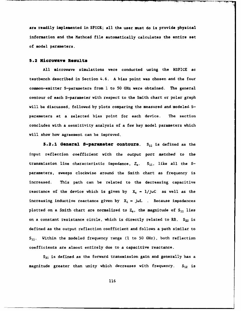
are readily implemented in SPICE; all the user must do is provide physical
information and the Mathcad file automatically calculates the entire set
of model parameters.
5.2 Microwave Results
All microwave simulations were conducted using the HSPICE ac
testbench described in Section 4.6. A bias point was chosen and the four
common-emitter S-parameters from 1 to 50 GHz were obtained. The general
contour of each S-parameter with respect to the Smith chart or polar graph
will be discussed, followed by plots comparing the measured and modeled S-
parameters at a selected bias point for each device. The section
concludes with a sensitivity analysis of a few key model parameters which
will show how agreement can be improved.
5.2.1 General B-parameter contours. S11 is defined as the
input reflection coefficient with the output port matched to the
transmission line characteristic impedance, Z.. S11, like all the S-
parameters, sweeps clockwise around the Smith chart as frequency is
increased. This path can be related to the decreasing capacitive
reactance of the device which is given by X, - l/jwC as well as the
increasing inductive reactance given by X, - jwL . Because impedances
plotted on a Smith chart are normalized to Z., the magnitude of S11 lies
on a constant resistance circle, which is directly related to RB. S22 is
defined as the output reflection coefficient and follows a path similar to
S11. Within the modeled frequency range (1 to 50 GHz), both reflection
coefficients are almost entirely due to a capacitive reactance.
S21 is defined as the forward transmission gain and generally has a
magnitude greater than unity which decreases with frequency. S12 is
116

defined as the isolation or feedback of the device. The magnitude of S12
is small at low microwave frequencies and increases with frequency.
5.2.2 Comparimon of modeled and measured S-paramoter..
The additional model parameters that characterize the device's ac
performance deal with the transport, removal, and storage of charge.
These parameters are the zero-bias depletion capacitances (CJE and CJC),
the junction grading factors (tMlE and MJC), the built-in junction voltages
(VJE and VJC), the forward and reverse base transit times (TF and TR), and
the internal capacitance ratio (XCJC). All of these SPICE model
parameters, along with the dc bias, are used to calculate the th .ee
hybrid-7 equivalent circuit (see Fig. 4.8) capacitors: C,, Coint, and C,,,t.
The six additional parasitic elements (see Fig. 4.9) were calculated by
Mathcad and added to the microwave HBT model. The leakage resistors
described by Eq. (4.45) were calculated to be in excess of 106 0. Placing
a resistor of this magnitude in parallel with each of the three parasitic
capacitors Cbep, Cbcp, and C.ep barely had a fourth decimal place effect on
the modeled S-parameters because the impedance of the capaciters was so
much smaller. Therefore, pad leakage resistors are not included in the
model.
Table 5-6 summarizes the complete list of SPICE model parameters for
the 3uldlf device, including all parasitics. As before, all parameters
with the exception of NF, NE, and NC are physically calculated. Figures
5.14 - 5.17 compare the modeled and measured S-parameters for the 3uldlf
device at a moderate bias of VCE - 2 V and IB - 100 pA. The I-V
characteristics of Fig. 5.3 clearly show that the device is operating in
the forward active region which is typical for small-signal applications.
117

Table 5-6
3uldlf SPICE BJT Full Model Parameters
BF - 28.90 TF - 0.95681 ps
BR - 0.005 TR - 0.52870 ns
NF - 1.116 CJE - 9.8515 fF
NR - 1.0000 CJC - 11.190 fF
RE - 33.6707 Q MJE - 0.50
RB - 9.3857 Q MJC - 0.50
Rbext - 33.8989 0 VJE - 1.7018 V
RC - 67.800 0 VJC - 1.3691 V
IS - 1.0363 x 10⁻²⁶ A XCJC - 0.2053
Lep - 1.6965 pH cceP -0.100 fF
4p- 1.6965 pH Cb.p - 0.739 fF
Lop - 3.3090 pH CbCP - 15.00 fF
118

Bias point
lb 100 uA
Vc e 2v
AMeasured
o Modeled
* Modeled with porasitics
0*
Figure 5.14 Comparison of S1, for the 3uldlf device from 1 to 50 GHz.
Bias point
lb = 1 00 uA-----
Vc e 2 v
0.24 0.16 0.08 - 0.08 0.16 0.24
* Measured
o Modeled
* Modeled with parasitic S
Figure 5.15 Comparison of S12 for the 3uldlf device from 1 to 50 GHz.
119

Bias point
lb = 100 uA
Vce = 2 v
:A ;,': .... .I . . . . .. • . . . . .. . •. .. . . . . .. ". ...... .. i.. . . . . . . . i . . . . . ... .. .. . . . . . . .
.5 1.0 0.5, 0.5 1.0 1.5
* Measured
o Modeled
* Modeled with parasitics
Figure 5.16 Comparison of S21 for the 3uldlf device from I to 50 GHz.
Bias point
lb = 100 uA
Vc e =2 v
A Measured
O Modeled
* Modeled with parasitic s
Figure 5.17 Comparison of S22 for the 3uldlf device from 1 to 50 GHz.
120

The comparison of S11 in Fig. 5.14 shows excellent agreement between
the modeled and measured data. Notice that two sets of modeled data are
plotted. One set is merely the linearized version of the dc model, or the
hybrid-r circuit of Fig. 4.8. The other set was produced by the full
model with physics-based values for all six parasitics. The importance of
accurate parasitic modeling is seen by how much closer the full model
comes to the measured data. The full model curve follows practically the
same constant resistance circle as the measured curve. This is a result
of the accurate calculation of RB. In fact, the value of RB can be
estimated from S1. Notice that the measured curve follows the r - 0.8
circle which, being normalized to 50 Q, correlates to an RB of 40 Q. The
Mathcad file calculated the sum of the intrinsic and extrinsic base
resistances at 43.28 1.
The 3uldlf comparison of S12 is shown in Fig. 5.15. The full model
curve starts off well but as frequency increases the angle does not
decrease rapidly enough. Because the measured curve lies within the two
sets of modeled data, one or more parasitics may have been overestimated.
CbP is a suspect since a smaller value will increase the impedance between
the base and collector. This should minimize coupling and reduce $12.
S21 for the 3uldlf device is shown in Fig. 5.16. The modeled curves
have the same general shape but the gain is too large, especially at the
lower frequencies, and the angle at higher frequencies does not drop
enough. A small increase in RE will pull the gain down at low frequencies
but will not effect the angle at the high frequencies. Figure 5.17 shows
the comparison for S22. Adding parasitics clearly took a step in the right
direction, but fell short since the full model curve lies in between the
bare model (without parasitics) curve and the measured curve.
121

Similar plots are shown in Figs. 5.18 - 5.21 for the 3u5dlf device
at a moderate bias of Vc - 2 V and ID - 300 #A. The complete list of
SPICE model parameters for the 3u5dlf device is shown in Table 5-7. The
full model for S11 (Fig. 5.18) improves the angle so that the modeled and
measured curves are no longer askew. Notice that the full model's
magnitude is initially less than that of the measured points. The modeled
and measured points converge at 3 GHz, and then the measured magnitudes
are less for frequencies above 4 GHz. Although the reason is not obvious,
this occurrence could be attributed to C,,*t being split across the base
resistance.
The full model curve for S12 shown in Fig. 5.19 matches the measured
data better than the model without parasitics, though both need to extend
below the zero angle line at higher frequencies. This same problem will
be discussed in more detail with the 2u6d2f device. The 3u5dlf S21 full
model data has better agreement than the 3uldlf S21, however; both models
suffer from too large a magnitude in the low frequencies. The measured
3u5dlf S22 has a unique curve that follows a constant resistance circle up
through 6 GHz then runs straight across the Smith chart, almost as if some
capacitive and inductive reactances are competing to decide the path.
Both of the modeled curves follow constant resistance circles for nearly
the entire 50 GHz range. The model without parasitics follows the r - 1.1
circle and the full model follows the r - 0.6 circle. The full model
begins to bend downward but only at the uppermost frequencies.
The bare model data of both of the one finger devices are relatively
far apart from the measured data. This could indicate that the one finger
devices have parasitics that are comparable to the intrinsic device
impedances. The intrinsic device can be thought of as being surrounded by
122

Table 5-7
3u5dlf SPICE WJT Full Model Parameters
BF - 33.30 TF - 0.95811 ps
BR - 0.0231 TR - 1.40460 ns
NF - 1.1557 CJE - 49.257 fF
MR - 1.0000 CJC - 35.706 fF
RE - 6.7341 Q WEE- 0.50
RB - 1.8771 0 MJCr- 0.50
Rbext - 6.7798 fl VJE - 1.7018 V
RC - 16.79 17 VJC - 1.3454 V
IS - 5.2047 x 10⁻²⁶ A XCJC - 0.2053
Lep - 1.4224 pH Cep- 13.650 fF
Lbp- 8.4823 pH Cbep - 3.6943 fF
Lcz - 1.7090 pH Cbep,- 31.566 fF
123

Bias point
lb = 300 uA
Vc e 2 v
* Measured
O Modeled '
* Modeled with parasitic s
Figure 5.18 Comparison of S1, for the 3u5dlf device from 1 to 50 GHz.
Bias point
lb = 300 uA ------
Vc e 2 v
0
0.2ý4 0.1 6 0.08008 1 0.4F1 G Hz
A Measured --
O Modeled
* Modeled with parasitics
Figure 5.19 Comparison of S12 for the 3u~dlf device from 1 to 50 GHz.
124
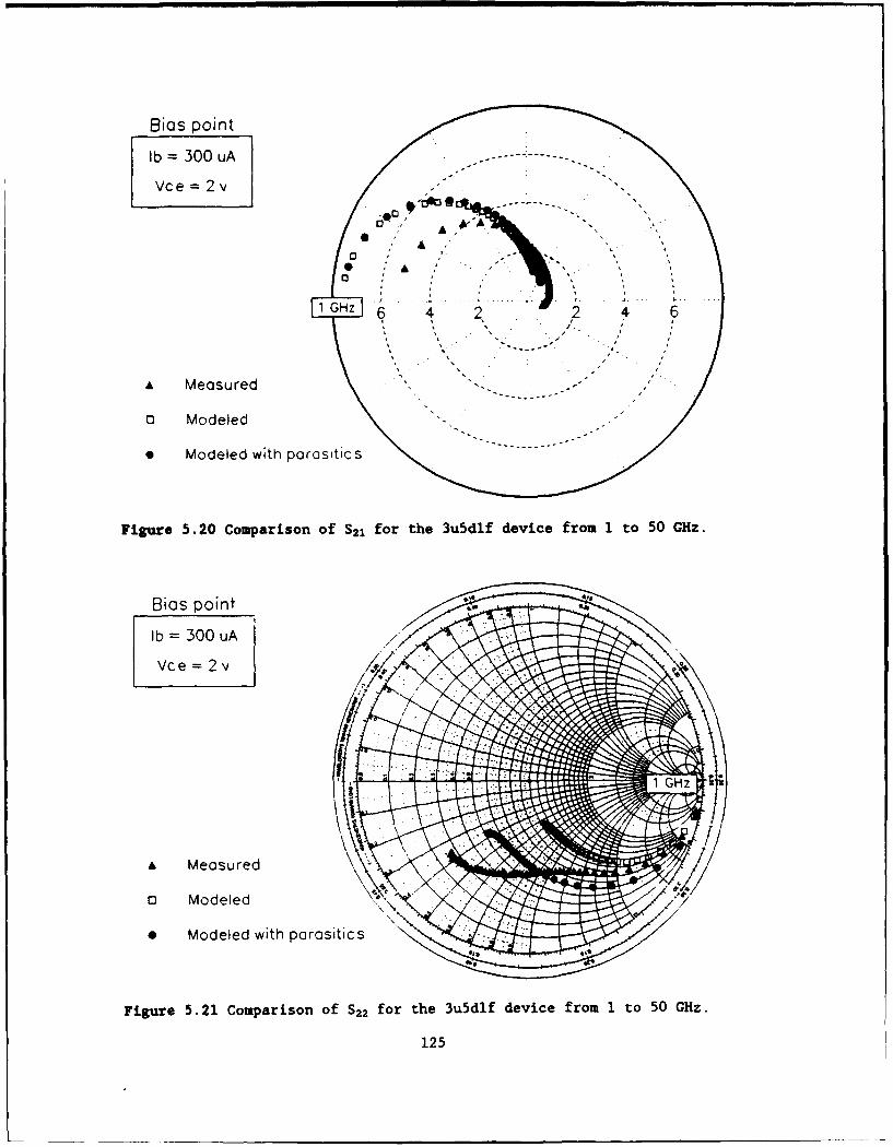
Bias point
lb = 300 uA
Vc e =2 v
* Measured
* Modeled
* Modeled with parasitic s
Figure 5.20 Comparison of S21 for the 3u~dlf device from 1 to 50 GHz.
Bias point
lb =300 uA
Vc e 2 v
A Meosured
o Modeled
* Modeled with parasitics
Figure 5.21 Comparison of S22 for the 3u5dlf device from 1 to 50 GHz.
125

a shell of series inductances and a shell of shunt capacitances [31]. If
the S-parameters of these shells are large with respect to those of the
intrinsic device, then their effect is pronounced and accurate modeling is
even more important.
The bare model S-parameters of the 2u6d2f device are close to the
measured S-parameters. Analogous to the one finger devices, this could be
attributed to the relatively small contribution of the parasitic shells.
Very good to excellent agreement was obtained on all of the 2u6d2f S-
parameters as shown in Figs. 5.22 - 5.25. The full set of 2u6d2f model
parameters is listed in Table 5-8. The S-parameters were measured in the
active mode with a bias of VCE - 1 V and ID - 800 ,sA. Although their
equivalent circuits are related by linearization, dc model agreement is
not the strongest factor influencing microwave agreement. At the bias
point chosen for S-parameter simulations, the 3uldlf and 3u5dlf devices
have about a 1 and 0.3% difference, respectively. The 2u6d2f device has
about a 3% difference, yet the S-parameters for the 2u6d2f device have
better agreement than the other two devices.
The bare model S11 follows nearly the same constant resistance circle
(r - 0.2) as the measured S11 shown in Fig. 5.22. The effect of the
parasitics on the model was to shift S11 clockwise around the Smith chart
(increasing inductive reactance), especially in the 1 to 7 GHz frequency
range. The combination of the parasitic and intrinsic device reactances
resulted in S11 having less capacitive reactance at the lower frequencies.
Additionally, the magnitude increased slightly at the higher frequencies.
To complete the agreement, the modeled data points need to be spread out
more at the higher frequencies to enter the inductive reactance region of
the Smith chart. The model parameter changes required to obtain better
126

Table 5-8
2u6d2f SPICE LIT Full Model Parameters
BF - 83.926 TF - 0.95243 ps
BR - 0.6338 TR - 0.12611 ns
NF - 1.1049 CJE - 48.855 fF
NR - 1.0000 CJC - 157.58 fF
NE - 1.7000 WJE - 0.50
NC - 1.7595 MJC - 0.50
ISE - 2.432 x 1 0 -ia A VJE - 1.7018 V
ISC - 4.393 X 10⁻¹⁷ A VJC - 1.4107 V
IS - 1.111 x 10⁻²⁵ A XCJC - 0.1590
RE - 6.7896 0 RC - 2.200 0
RB - 0.7821 0 Rbext - 4.0557 Q
Lp - 0.4841 pH CceP - 18.488 fF
Lbp- 2.3562 pH Cbp - 7.3255 fF
Lcp 0.6093 pH Cbcp - 106.13 fF
127

Bias point
Ib =800 uA
Vce =1 VN
A Measured
o Modeled
* Modeled with parasities
Figure 5.22 Comparison of S1, for the 2u6d2f device from 1 to 50 GHz.
Bias point
lb = 800 uA-- -----
0.1 18 0.1 12 0.06 0.06 0.112 0
* Measured- - - -- - -
* Modeled
* Modeled with parasiti.c s
Figure 5.23 Comparison of S12 for the 2u6d2f device from 1 to 50 GHz.
128
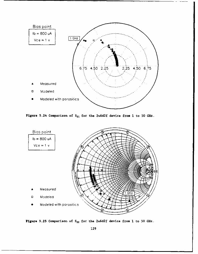
Bias point
lb = 800 uA ---
Vce 1 v A l,
6.75 4.50 2.25 2.25 4.50 6.75
* Measured
o Modeled
* Modeled with parasitics-
Figure 5.24 Comparison of S21 for the 2u6d2f device from 1 to 50 GHz.
Bias point
lb =800 uA
Vce 1 v
* Measured
o Modeled
* Modeled with parasitic s
Figure 5.25 Comparison of S22 for the 2u6d2f device from 1 to 50 GHz.
129
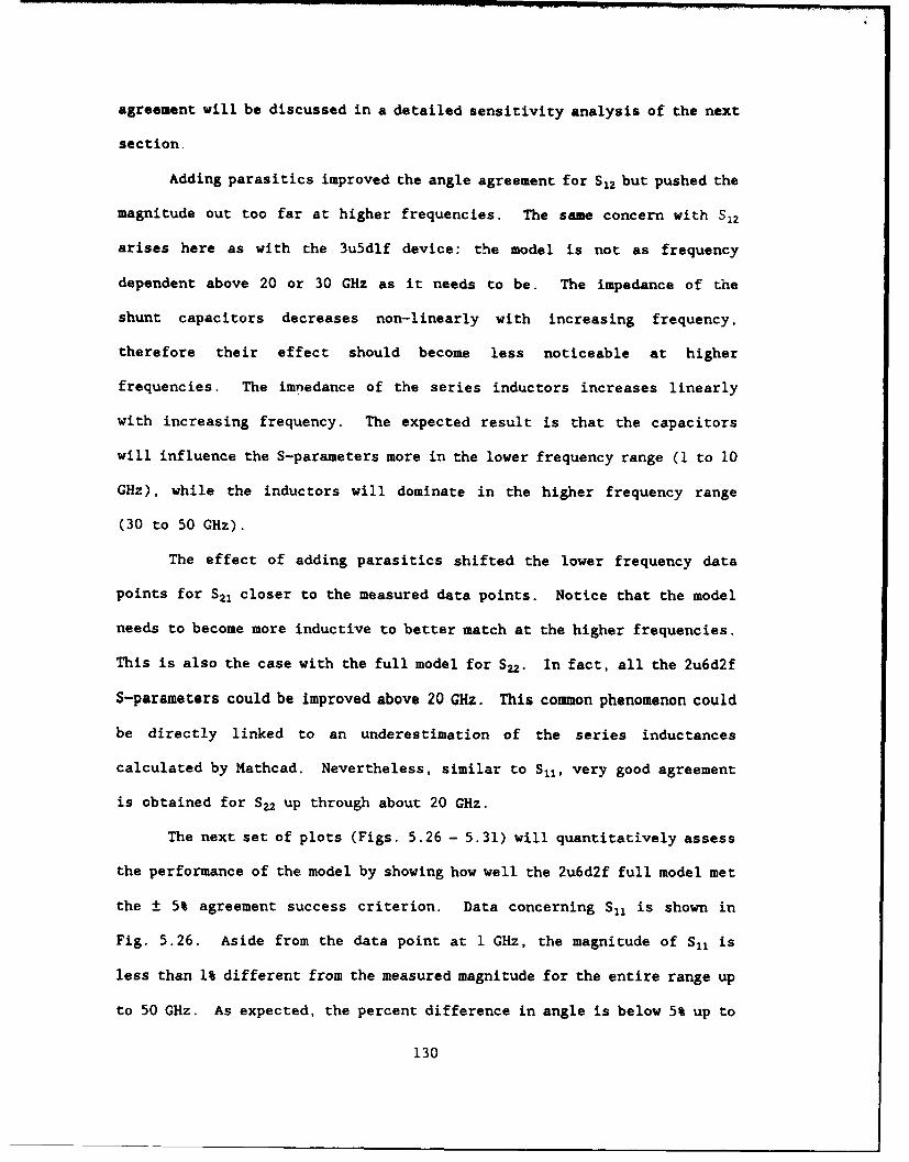
agreement will be discussed in a detailed sensitivity analysis of the next
section.
Adding parasitics improved the angle agreement for S12 but pushed the
magnitude out too far at higher frequencies. The same concern with S12
arises here as with the 3u5dlf device: the model is not as frequency
dependent above 20 or 30 GHz as it needs to be. The impedance of the
shunt capacitors decreases non-linearly with increasing frequency,
therefore their effect should become less noticeable at higher
frequencies. The imnedance of the series inductors increases linearly
with increasing frequency. The expected result is that the capacitors
will influence the S-parameters more in the lower frequency range (1 to 10
GHz), while the inductors will dominate in the higher frequency range
(30 to 50 GHz).
The effect of adding parasitics shifted the lower frequency data
points for S21 closer to the measured data points. Notice that the model
needs to become more inductive to better match at the higher frequencies.
This is also the case with the full model for S22. In fact, all the 2u6d2f
S-parameters could be improved above 20 GHz. This common phenomenon could
be directly linked to an underestimation of the series inductances
calculated by Mathcad. Nevertheless, similar to S11, very good agreement
is obtained for S22 up through about 20 GHz.
The next set of plots (Figs. 5.26 - 5.31) will quantitatively assess
the performance of the model by showing how well the 2u6d2f full model met
the ± 5% agreement success criterion. Data concerning S1 is shown in
Fig. 5.26. Aside from the data point at 1 GHz, the magnitude of S1 is
less than 1% different from the measured magnitude for the entire range up
to 50 GHz. As expected, the percent difference in angle is below 5% up to
130

9
Q) 7Cq) 6
•- 54
"O• 3
C 2
UUIP- -1
1 4 7 10 13 16 19 22 25 28 31 34 37 40 43 46 49
Frequency (GHz)
Figure 5.26 Percent difference between the modeled and measuredmagnitude of S1, for the 2u6d2f device at a I V, 800 pA bias.
0
-2 FS" 4
C -6
"- -81
S-o o
Co -12
• -14
-16
1 4 7 10 13 16 19 22 25 28 31 34 37 40 43 46 49
Frequency (GHz)
Figure 5.27 Percent difference between the modeled and measured angle of
SI1 for the 2u6d2f device at a 1 V, 800 AA bias.
131

3II
) 2
C
Q)
I*-
"-0 0
C0 -1
EC1404 -2
3_ 1 , 1 1 1111I I 11I II1 II1 I I 1 I 1 1 I
1 4 7 I1C 13 16 19 22 25 28 31 34 37 40 43 46 49
Frequency (GHz)
Figure 5.28 Percent difference between the modeled and measuredmagnitude of S22 for the 2u6d2f device at a 1 V, 800 AA bias.
3
S -1
U1)"U) -3
U)
CrC -7
-11I I I I I I I I I I I I I I I I I I I I IIII h u I I I1 1 1 1 I l Ii i I I I I I i I IS
1 4 .7 10 13 16 19 22 25 28 31 34 37 40 43 46 49
Frequency (GHz)
Figure 5.29 Percent difference between the modeled and measured angle
of S27 for the 2u6d2f device at a I V, 800 AA bias.
132

?18
c 16
Q 14
1 12
aI) 10
SII8C
o 6E(N 4
2
0 LI11 Illllll Il IL'
1 4 7 10 13 16 19 22 25 28 31 34 37 40 43 46 49
Frequency (GHz)
Figure 5.30 Percent difference between the modeled and measuredmagnitude of 512 for the 2u6d2f device at a 1 V, 800 pA bias.
CI
C -3
-5Q~)-0 -7
C _
0E i
S-13
-15 a1 4 7 10 13 16 19 22 25 28 31 34 37 40 43 46 49
Frequency (GHz)
Figure 5.31 Percent difference between the modeled and measured
magnitude of S21 for the 2u6d2f device at a 1 V, 800 pA bias.
133

about 17 GHz. The angle difference clearly increases linearly with
frequency; a strong indication that the inductance is underestimated.
Similar to S11 , the magnitude of S2 shows excellent agreement by
differing less than 3% for the entire 50 GHz range. Again, the percent
difference in angle increases linearly with frequency providing further
support of underestimated inductance. The model is successful in modeling
S22 up to approximately 27 GHz.
Because the angle data for both S12 and S21 at the higher frequencies
is relatively small, a plot of the percent angle difference is not a
valuable metric in quantifying model performance. Clearly, the full model
for both of these parameters is more accurate at the lower frequencies.
Evidence supports an underestimation of the parasitic inductance .ý the
primary cause for the limited agreement. The percent difference in the
magnitudes of S12 and S21 is shown in Figs. 5.30 and 5.31. The difference
in magnitude for S12 averages about 13% up to 28 GHz, and stays less than
18% over the entire frequency range. The difference in magnitude for S21
reaches a maximum of just over 13% at around 6 GHz and then decreases
almost linearly for the rest of the frequency range. The difference in
magnitude as well as the angle for these two gain parameters is expected
to be improved by increasing the parasitics inductances. This will be
confirmed in the section on sensitivity analysis.
Overall, this novel approach to a physics-based microwave HBT model
produces fair agreement for all three devices. By inspection, one can see
that the agreement for the 2u6d2f device is much better than for the one
finger devices. As mentioned earlier, the main reason for this is
expected to be the relative dominance of parasitics with respect to the
intrinsic device in the one finger devices. Because the bare model data
134

for the 2u6d2f device is on average less than 250 from the measured data
(magnitude and angle), the full model provides an adequate testbench for
determining model parameter sensitivities.
5.2.3 Model parseter sensitivity analysis. The sensitivity
analysis was performed by starting with the 2u6d2f model parameters as
calculated by the Mathcad file. The value of each parasitic capacitor was
increased and decreased by a factor of five. Similarly, since the need
for increased inductances had already been hypothesized, the value of L.,
and 4p was increased by an order of magnitude; 1,, was increased by two
orders of magnitude to realize the expected changes. Additionally the
impacts of decreasing CJE and CJC by a factor of five were investigated.
Because CJE and CJC are the zero-bias depletion capacitances, a
proportional change will be seen in C, and C., respectively. Recall that
C, and C. are the total junction capacitances (depletion and diffusion)
dependent on bias as well as all the SPICE ac model parameters.
Each model parameter variation was treated as a control. The
resulting HSPICE S-parameter data for each variation was compared to the
original full model data to determine the effects that each parasitic had
on model performance. The results are shown in Tables 5-9 through 5-15.
For clarity and ease of visualization, the changes in angle (L) data are
listed as either clockwise (cw) or counterclockwise (ccw) shifts around
the Smith/polar charts. IMI is used as an abbreviation for magnitude.
Also, in this context, low frequency refers to the 1 to 10 GHz range and
high frequency refers to the 20 to 50 GHz range. The following
qualitative definitions are used in Tables 5-9 through 5-15: significant
for changes of greater than 25%, slight for changes of less than 20%, and
minimal for changes of less than 10%.
135

Table 5-9
Sensitivity of Cbcp on S-parameters
Sij Effect on modeled S-parameters
- When decreased, shifted the L ccw significantly at low fand decreased the IMI at high f.
S11 - When increased, shifted the L cw significantly at low f and
increased the IMI at high f.
- When decreased, decreased the IMI at all f and increasedthe range of L spread.
S12 - When increased, increased the IMI at all f and reduced the
range of L spread.
- When decreased, increased the IMI and shifted the L ccw atall f.S21 - When increased, decreased both the 4MI and shifted the L cw
significantly at all f.
- When decreased, shifted the L ccw significantly at low f,decreased the IMI at high f, and increased the IMI at low I.
S22 - When increased, shifted the L cw significantly at low f,increased the IMI at high f, and significantly reduced theIMI at low I.
Table 5-10
Sensitivity of Cbkp on S-parameters
Sjj Effect on modeled S-parameters
S11 - Negligible effect.
- Minimal effect at low I.S12 - Slight effect at high I.
S21 - When increased, shifted the L cw minimally at high f.
S22 - Same as for S12.
136

Table 5-11
Sensitivity of C0*, on S-parameters
SU Effect on modeled S-parameters
S11 - When increased, decreased the IMI slightly at all f.
- When increased, both decreased the IHI and shifted the L cvS12 significantly at high f.
- When increased, decreased the IMI minimally for all f, andS21 shifted the L cw at high f.
- When increased, increased the 1IM and shifted the L ccw atS22 high f
Table 5-12
Sensitivity of CJC on S-parameters
Sij Effect on modeled S-parameters
- Increased the IMI and shifted the Z ccw significantly ataS11 low f, and increased the IMI at high f.
- Decreased the IMI significantly and shifted the L ccw atS 12 l o w
'Zif.lS21 - Increased the IMI and shifted the £ ccw at all f.
- Both increased the IMI and shifted the L ccw significantlyat low f, and decreased the IMI at high I.
137

Table 5-13
Sensitivity of L, on S-parameters
SiJ Effect on modeled S-parameters
S21 - Minimal effect.
S12 - Shifted L cw at high f.
S2 E l - Increased the IMI slightly at high f.
S2 - Minimal effect.
Table 5-14
Sensitivity of L,, on S-parameters
Sjj Effect on modeled S-parameters
S11 - Negligible effect.S - Decreased the IMI and shifted L cv significantly at high f.S21 - Shifted the L cw at high f.
- Increased the IMI slightly and shifted the L cwS22 significantly at high f.
Table 5-15
Sensitivity of 4. on S-parameters
Sjj Effect on modeled S-parameters
S11 - Shifted the L cw significantly at high f.
S12 - Shifted the L cw significantly at high f.
S21 - Shifted the L cw at high f.
S22 - Negligible effect.
138

The inverse relationship that CbQp has on S21 and S12 is easily
conceptualized. Because S21 and S12 represent the forward and reverse
transmission gains, respectively, their magnitudes are most effected by
the base-collector parasitic capacitor that couples the input and output
ports. Naturally, for a large gain the coupling between the input and
output ports should be minimized (isolated). Increasing Cbcp increases the
coupling between the ports which reduces gain (S21) and increases feedback
(S12) throughout the frequency range modeled. Cbcp also serves to shift S11
and S22 along constant resistance circles at low frequency. A decrease in
Cbcp increases capacitive reactance so each point on the curve is shifted
counterclockwise, i.e. in the direction of increasing capacitive reactance
on the Smith chart. This effect is significant only at low frequencies
because the increase in reactance is inversely proportional to frequency.
An increase in C,,, primarily decreases feedback and shifts the S12 curve
clockwise at high frequency. By symmetry, Cb•p will have the same effect.
This change in S12 is one of the desired improvements identified in
Fig. 5.23.
Reducing CJE by a factor of five had a negligible effect on the S-
parameters. The reason for this is that under forward bias, C, is
relatively large and mostly diffusion capacitance. Therefore, any change
in CJE will manifest only a small change in C,. In fact, the script
generated by HSPICE during each ac simulation (which lists the hybrid--*
equivalent circuit element values), showed that reducing CJE by a factor
of five only reduced C, from 749 fF to 692 fF.
Reducing CJC by a factor of five had significant effect on all of
the S-parameters, especially at low frequency. Under reverse bias both
Culnt and C,.1t are dominated by their depletion components. Thus, reducing
139

CJC by a factor of five reduces both Cjt and Ct by a factor of five.
Because all three base-collector capacitances (Cnt, C•, and Cbp) are to
a first order approximation in parallel, the change in CJC effectively
cuts the total base-collector capacitance in half.
The influence of LIt and LI. on the modeled S-parameters is exactly
as envisioned in the last section. Increasing these two parameters will
substantially improve the model's high frequency performance. As one
might expect, Lp has a negligible effect on S1. By symmetry, L.. has a
negligible effect on S11. Testbench simulation with HSPICE also shows that
superposition of their independent results applies. That is, changing
both L4 and Lcp simultaneously effects the S-parameters by an amount equal
to the sum of their individual effects on the S-parameters.
Based on the data observed while conducting the sensitivity
analysis, increasing the parasitic inductances should provide excellent
agreement through 50 GHz. Increasing the Mathcad values of Lp by a factor
of 20, and Lp by a factor of 50 (which would result in 4. = 47 pH and
L=p - 30 pH) is recommended. Several published HBT models have extracted
values for these series inductances through various curve fitting and
measurement techniques [28,31,72,73,76]. Each of these other models
reports series inductances on the order of tens of picohenries.
Table 5-16 compares the 2u6d2f model parasitics with the parasitics
of other published HBT models having similar equivalent circuits. Aside
from one low value reported for 4. [72], all of the 2u6d2f inductance
values are from one to two orders of magnitude smaller than other
published values. Another observation is that the 2u6d2f CbCp value
appears to have been overestimated.
140

At this point in the model derivation, the six parasitic values for
the 2u6d2f device were optimized in HSPICE by fitting modeled S-parameters
to measured S-parameters. The same bias (Vcz - 1 V and ID - 800 jsA) was
used in the optimization for consistency. Table 5-17 shows the optimized
parasitics. A comparison of the resulting S-parameters is shown in Figs.
5.32 - 5.35. The prediction that increasing Lt. and L,, to 47 pH and
30 pH, respectively, would provide excellent agreement up through 50 GHz
was confirmed. HSPICE optimized Lbp and Lp at 44.35 pH and 28.68 pH,
respectively. Figures 5.32 - 5.35 clearly show the very good to excellent
agreement that all four S-parameters have up through 50 GHz.
To summarize, an underestimation of the parasitic base and collector
series inductances was suspected as the reason for the good to poor S-
parameter angle agreement at frequencies greater than 30 GHz. The
sensitivity analysis assisted in predicting estimates for Lbp and L,, that
would provide excellent agreement up through 50 GHz. HSPICE optimization
validated underestimation of Lbp and L,, as the cause of the high frequency
disagreement. The next step was to physically justify the optimized
parasitic values. In other words, can the optimized parasitic values be
substantiated using only a knowledge of the device material, geometry, and
fabrication process.
The Mathcad equations for parasitic calculations were examined to
see if any physical components of L4p and L~p were overlooked. In
calculating 14. and Lp, only the portion of planar transmission line
beneath the emitter bridge was considered. In reality, each of the
devices modeled had a grounded backplane separated from the base and
collector metals by 70 microns of GaAs substrate. Therefore, the grounded
backplane forms a transmission line with the base and collector
141

Table 5-16
Comparison of 2u6d2f Parasitics With Other HBT Models
Parasitic 2u6d2f Ref (31] Ref (71] Ref (74]
L.1 (pH) 0.4841 12 39 10
L,,p (pH) 2.3562 47 1 30
L1 p (pH) 0.6093 50 60 49
Cb©p (fF) 106.13 3 2 6.3
CbP (fF) 7.3255 13 3 40
Ccep (fF) 18.488 20 13 31
Table 5-17
Optimized Parasitics for the 2u6d2f Device
Parasitic Initial LoW High Optimized
Lp (pH) 15 0.3 30 1.71
4p (pH) 40 8 85 44.35
Lop (pH) 20 5 50 28.68
Cbcp (fF) 7.6 1 114 76.01
Cbp (fF) 6 1 30 26.42
Cep (fF) 18.5 3.7 92.5 76.18
142
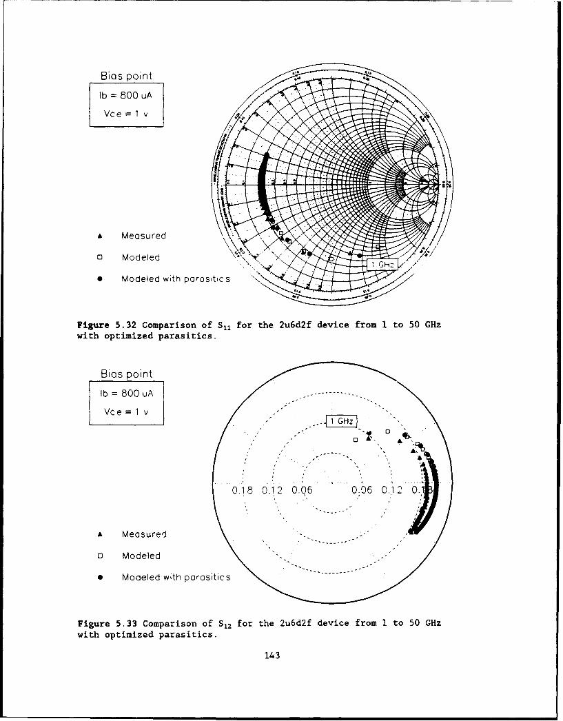
Bias point
Ib = 800 uA
Vce = v
* Measured
o Modeled
* Modeled with parasitic s
Figure 5.32 Comparison of S11 for the 2u6d2f device from 1 to 50 GHzwith optimized parasitics.
Bias point
lb = 800 uA -- -.
Vce=1 v
" , ~0 "•,0 ,
0.18 0.12 0.06 0.06 0.12 0.1
A Measured
o Modeled
* Modeled with parasitics
Figure 5.33 Comparison of S12 for the 2u6d2f device from 1 to 50 GHzwith optimized parasitics.
143

Bias point
lb =800 uA
Vce =1 v F HýC,
67*5 4.50 2.25 2;25 4.50 6.75
* Measured
O Modeled
* Modeled with parasitic s
Figure 5.34 Comparison of S21 for the 2u6d2f device from 1 to 50 GHzwith optimized parasitics.
Bias point
lb = 800 uA
Vce =1 v
... ../
A Measured
o Modeled X
* Modeled with porcisitics
Figure 5.35 Comparison of S22 for the 2u6d2f device from 1 to 50 GHz
with optimized parasitics.
144

interconnect metals between the pad and emitter bridge. The contribution
of this transmission line configuration to l. and Lp is much greater than
the contribution of the transmission line approximation beneath the
emitter bridge. The reason for this is because planar transmission line
inductance is proportional to the separation between the conductors.
Since the thickness of the substrate (- 70 microns) is 25 to 70 times the
separation between the conductors beneath the emitter (one to three
microns), the component of Lbp and Lp beneath the emitter bridge is almost
negligible. However, the parallel combination of Lbp and LP beneath the
emitter bridge is still a fair approximation for L,. This is assumption
is substantiated by the relatively low optimized value of Lp.
The calculated 4p and LP due to the interconnect metals between the
pad and emitter bridge was approximately a factor of three larger than the
optimized 4.p and L,,. One explanation is that the simple planar
transmission line inductance equation does not accurately predict the
actual inductance. This is most likely because the actual geometry is not
a planar transmission line.
In Chapter 4, Cbp and C,,, were estimated using the parallel plate
approximation. Due to the complex emitter geometry, one could theorize
that the actual values of Cb~p and C,., would be two to three times greater
than the parallel plate values. This assumption is validated by the
Mathcad values for Cb.p and Cc.p, which are approximately two to three times
smaller than the optimized values. Any contributions to Cbop and C,,p due
to the grounded backplane are negligible, since parallel plate capacitance
is inversely proportional to plate separation.
In summary, the attempt to physically substantiate the optimized
2u6d2f parasitic values resulted in capacitances that were two to three
145

times smaller than the optimized values, and inductances that were two to
three times larger than the optimized values. Although larger
capacitances are easy to conceptualize based on the geometry, they are too
difficult to accurately calculate with a simple formula. Accurate
parasitic values are best obtained using a special electromagnetic
software package that can recognize random three dimensional transmission
line geometries.
Table 5-18 compares the 2u6d2f SPICE bare model parameters with the
parameters from other published HBT SPICE models. Obviously, since each
of the HBTs characterized by the various model parameters has differences
in geometry and fabrication, the listing provides only a rough comparison.
The results show that the 2u6d2f model is a sound physics-based HBT model;
all of the parameters are roughly the sAme magnitude as the other model's
parameters. Any differences in the model parameters can be attributed to
differences in the device material, geometry, and fabrication process.
Some of the differences between the various models will now be discussed.
There are two ways to model recombination in the extended Ebers-Moll
topology. The first provides more insight into the effects of
recombination since four model parameters are needed to characterize.
This entails calculating (or measuring) the composite recombination
saturation currents ISE and ISC along with their corresponding ideality
factors, NE and NC. The second method will generally give better results
since it is less prone to errors; however, some of the physical insight
into the various recombination mechanisms is lost. In this method, ISE
and ISC are set to zero and all recombination is accounted for in an
empirical value of PF.
146

Table 5-18
Various HBT SPICE Model Parameters
Param. Ref(78] Ref[25] Reff26] Ref[71] Ref[77] 2u6d2f
BF 3.444 300 52.52 169 83.93
BR 2.le-07 0.40 0.1987 0.1 0.6338
TF, s 1.51e-12 4.3e-12 3e-12 4e-12 9.52e-13
TR, s 3.5e-10 1.26e-10
IS, A 1.67e-26 5.00e-25 4.84e-24 9.4e-26 8.0e-24 I.ile-25
ISE, A 4.00e-17 2.46e-18 2.39e-16 3.0e-20 2.43e-19
ISC, A 1.42e-14 5.93e-14 1.8e-14 4.39e-16
RE, fl 5.4 11.0 17.61 45 0.0 6.7896
RB, f0 30.7 37.3 122.23 150 34 4.8379
RC, fl 6.6 6.42 10.26 51 6 2.205
CJE, F 3.5e-14 1.25e-13 8.6e-15 1.7e-14 4.89e-14
CJC, F 9.16e-15 3.95e-14 1.9e-14 1.58e-13
VJE, V 1.72 1.45 1.45 1.7 1.7018
Vic, v 1.40 1.18 1.4 1.21 1.4107
MJE 0.5 0.51 0.5 0.5 0.5
mi¢ 0.5 0.5 0.33 0.5 0.5
NF 1.16 1.021 1.1331 1 1.179 1.1049
NR 1.00 1.00 1.00 1.00
NE 1.186 1.8211 2 1.6 1.7000
Nc 1.950 1.9698 2 1.7595
XcJX 0.220 0.159
147

As discussed in earlier chapters, HBTs rarely have a region of
operation in which PF is constant. Because an HBT's recombination currents
are bias dependent, any empirical PF that accounts for recombination will
also be bias dependent. Unfortunately, SPICE expects a constant SF and
does not directly support a bias dependent BF. Recall from Eqs. (5.1) and
(5.2) that recombination modeled via ISE and ISC is automatically bias
dependent in SPICE, because the terms that include ISE and ISC are
functions of VDE- and VC, ,. Therefore, if an empirical BF is used to
account for bias dependent recombination in SPICE, one must write the
SPICE HBT model file with BF as a function of a known bias condition,
either IB or V3 E (reference Fig. 5.10 and related discussion). This
technique is sufficient for microwave simulations where the dc bias is
generally fixed, but may be impractical for dc applications where the bias
is variable.
Of the model's presented in Table 5-18, Teeter et al.'s model [78]
is unique because their BF is an empirical PF. Although not shown in
Table 5-18, their BF is a function of VBE. As expected, their model does
not include values for ISE, ISC, NE, or NC.
Grossman's and Choma's model [25] is partly physical and partly
empirical. Their BF is physically calculated due only to bulk
recombination current in the neutral base. Consequently, values for ISE,
ISC, NE, and NC are needed to account for the other recombination
mechanisms present in the HBT. This method of modeling recombination was
used to model the 2u6d2f device. The difference between the reference
[25) and the 2u6d2f BF can be attributed to differences in base doping and
thickness. All the differences in the remaining model parameters can
148

likewise be attributed to differences in the geometry and fabrication
process.
The model of reference [711 uses physical parameters (material,
geometry, and fabrication process) as well as measured data to determine
the SPICE model parameters. Information on how each parameter is
specifically calculated is not available. Therefore, the parameters
listed provide only an example of the magnitude of each parameter that
SPICE uses to model their particular IBT.
Notice that Hafizi er al.'s model [26] is only a dc model, since
none of the charge storage, removal, and transport model parameters are
included. All of their model parameters were determined via convergence
of a least square fit to measured I-V data. These parameters are purely
curve fit and provide no meaningful basis for a physical comparison.
Matsuno et al.'s model [77] includes several passive elements
(diodes and resistors) external to the SPICE BJT model. Their RE is
modeled by an external resistor so the model card RE is set to zero.
Similar to Hafizi et al.'s model [26], Matsuno et al.'s HBT dc and ac
parameters are optimized via curve fitting to measured I-V data and S-
parameters, respectively. The specific optimization technique or package
is not specified. Again, the model parameters listed are merely those
that, given a particular equivalent circuit topology, best fit the
measured data. All insight into how the device material, geometry, and
fabrication process affect the model parameters (and thus, the electrical
performance) is lost.
149

6. Conclusions and Roomeniations
The objective of the research presented in this thesis was to derive
a physics-based model for an HET that would accurately predict the
device's electrical behavior from dc to microwave frequencies. A model
that considers a cylindrical emitter-base geometry and is directly
implemented into SPICE was developed. Using semiconductor physics, the
device model parameters were determined from a knowledge of the device
material, geometry, and fabrication process.
A Mathcad file was written which calculates all of the necessary
SPICE BJT model parameters required to accurately model an HBT. The dc
model was successful at producing data that was within ± 5% of the
measured data for two device geometries. dc model data for a third
geometry was an average of 6.73% different from the measured data. When
curve fit against measured data to determine ideality factors, the bias
dependent P and offset voltage of an HBT are accurately modeled.
Parasitic inductor and capacitor elements were physically determined
and added to the SPICE model. Poor to good agreement was obtained between
the resulting S-parameters for two of the device geometries; good to
excellent agreement was obtained for the third. Precise calculation of
the base and collector parasitic inductances was verified as the limiting
factor of the high frequency performance of the model. To the best of the
author's knowledge, this thesis is the first to report such good agreement
from a physics-based microwave HBT model.
More work needs to be accomplished to better model the devices in
saturation. A known limitation is the inability of SPICE to account for
the bias dependence of RC. If applications demand better agreement in
150

saturation, the SPICE source code could be modified to solve for RC
simultaneously with the base-collector junction voltage. However, this
procedure is not recommended since the ends would not justify the means.
A better analysis of the model's performance could be obtained by
comparison with measurements from more than one set of data for each
geometry. Because the model presented in this thesis is physics-based,
only theoretical data is modeled. Collecting measured data from more than
one device with the same geometry would assist in verifying the model's
ability to predict actual device performance. Measured data from the
other side of the wafer or even another wafer could themselves be ± 5%
different. Additionally, forward and reverse Gummel plots would provide
valuable insight into the device's saturation currents and ideality
factors. Gummel plots are well suited to graphical extraction of all
three saturation currents and the four ideality factors, because each of
these SPICE model parameters can be directly related to a slope or
intercept on the forward and reverse Gummel plots. Obviously, the common-
emitter I-V characteristics are dependent on the model saturation currents
and ideality factors; however, these parameters cannot be graphically
extracted as in the Gummel plots.
The model is easily modified to account for varying degrees of
graded or abrupt emitter-base heterojunctions as well as for graded base
or double HBTs by revising the appropriate equations in the Mathcad file.
Another improvement would be to account for HBTs fabricated from materials
other than AixGal-As/GaAs. Modeling HBTs of various materials (holding
the geometry and fabrication parameters constant) could be accomplished
readily by modifying the section on material constants and the empirical
mobility equations in the Mathcad file.
151

The most significant improvement would be the development of a full
electro-thermal model that considers all the effects of device self-
heating and heat dissipation. Almost all of the material parameters have
a temperature dependence described by equations that can be found in the
literature. Additionally, HSPICE has several BJT model parameters to
account for device performance as a function of temperature.
To the best of the author's knowledge, this thesis is the only
physics-based HBT model that attempts to model the effects of device
parasitics at microwave frequencies. All other microwave device modeling
techniques first measure the S-parameters and then curve fit the measured
S-parameters to a particular equivalent circuit topology. Parasitic
element values are optimized to best fit the measured S-parameters.
Using the expression for parallel plate capacitance, parasitic
capacitance element values were determined. Fringing was neglected with
the exception of base-collector capacitance, which is mostly a fringe
capacitance. To a first order approximation, the values determined should
be accurate.
Using the expression for the inductance of a planar transmission
line, parasitic inductance values were determined. From a strict
electromagnetic perspective, this method of calculating inductance is only
an approximation. The models developed in this thesis could be improved
by using more exact electromagnetic equations to calculate the parasitic
inductances and capacitances.
One may consider the emitter, base, and collector metallizations as
three planar sections of transmission line. The geometry and dielectric
constants are known. A program could be written (or an existing program
modified) to calculate the characteristic impedances of the set of
152

transmission lines in the transistor geometry. The parasitic inductances
and capacitances could then be determined from the characteristic
impedances and placed in the present HSPICE HIT model. The resulting
model would have more accurate parasitic element values and therefore be
more accurate at microwave frequencies. The novel result would be a
purely physics-based model that would perform as well as any curve fit
model. The best of both worlds would be obtained in such a model: the
incredible design flexibility and savings of a physics-based model with
the excellent accuracy of a curve fit model.
153

Appendix A: Kathoad Piles
A-1

HBT PHYSICAL PARAMETER CALCULATIONS
Author: James A. FellowsDate: 20 Nov 93FRlename: H 3uldlfmcdDescription: This program determines all of the model parameters required to characterize a gradedAlGaAs/GaAs heterojunction bipolar transistor (HBT) in SPICE. The calculated parameters will be placeddirectly into the SPICE BJT model card. Also calculated are the parasitic inductance and capacitanceequivalent circuit element values. All values are physically determined using a knowledge of only the devicematerial, geometry and fabrication process. Only three of the four ideality factors are empirically determined.Inputs: This program requires the device designer to input several specific fabrication constants. Thesevariables are included in the first section for convenience.
Fabrication Parameters:
N E =51017 AlGaAs emitter doping concentration (cma^-3)
N B =5.1019 GaAs base doping concentration (crn^-3)
N C =21016 GaAs collector doping concentration (cma^-3)
N subC =3.1011 Subcollector doping concentration (cma^-3)
I cap =3.10-6 Thickness of InGaAs emitter cap (cm)
N cap :=2-1019 Cap doping concentration (cmA-3)
I cgrad = 2.5. 10-6 Thickness of lnGaAs graded region (cm)
N cgrad 1 . 1019 Graded region doping concentration (cm^-3)
I E.cont 1 . 10'5 Thickness of GaAs emitter region (cm)
N E.cont = 5.10is GaAs doping concentration (cm^-3)
I grade =55.10-6 Thickness of AlGaAs graded region (cm)
N grade =5-0 170 AIGaAs graded doping concentration (cma^-3)
I wide = 5.10.6 Thickness of the AIGaAs emitter (cm)
X G :1.5-10- 6 Thickness of emitter-base junction grading (cm)
A-1

W :=7.10"6 Thickn of theGaAs bae (am)
IC =1'10y4 Thicknessofthe GaAscollector (cm)
1 subC = 1'10'4 Thickness of the GaAs subcollector (cm)
I ee :=3.10"4 Diameterof anemitter dot (cm)
N dot z I Number of emitter dots/finger
N fin 1 Number of base-cmitter fingers
I c :1.10- The length of the collector contact (cm)
Scl :9. 10' 4 The width of the collector contact (cm)
Ieb 1.10 04 The width of base finger contact on either side of emitter dot (am)
I bc : 2.10'4 The lateral distance between the base and collector contact (cm)
PEc =2"1076 Estimated emitter specific contact resistance (ohm.c^2)
PBc = 5. 10"6 Estimated base specific contact resistance (ohm.cma^2)
Abe N dot. N fin. ( -0.1.10")
A be =6.1575-10"- Base-emitter junction area (cmA2)
Abe =NdotN fm.(lee+2.10-4).(Ile.2)
Abc = 3 107' Base-collector junction area (cmA2)
XCJC be Fraction of base-collector area internal to device
Abe
P N finN dot- - 0..1 I) Total perimeter of emitter-base junction (cm)
A-2

db 110' Height of polyumide between the base and emittermetallizations (CM)
tcp =0.4.10'4 Thickness of collector pad metal (an)
lbb =lee+2.10'4 Width of base finger (cm)
t sub:= 70I0"'4 Thickness of GaAs substrate (cm)
General constants:
k = 8.61738. 10"s Boltzmann's constant (eV/K)
q - 1.602- 10- 19 Electron charge (C)
=8.854IU 14 Permittivity m vacuum (F/cm)
Io. =4.w.10-9 Permeability in vacuum (H/cm)
m o = 9.1095. 10-31 Electron rest mass (Kg)
T = 300 Temperature (K)
Material constants:
The only user defined constant is x, the mole fraction of A]. The expressions below are taken from thefollowing references [24, 55, 57, 59].
x :0.35 Mole fraction of Al in the emitter
E g : 1.424 + 1.247.x Band-gap energy of the AlGaAs emitter (eV)
I
AE gB = 1.6.10-'.N B3 Band-gap shrinkage in the GaAs base (eV)
A-3

E B -- 1.424 - AE Band-gapegy of the GaAs ba (eV)
AiE =EgE- Eg Band-gap differece at the abrupt emitter-base heterwcucm(eV)
t z 13.18 - 3.12. x Relative permittivity of the AIGaAs emitter
EB a = 13"18'Eo Permittivity of the GaAs base (F/cm)
CE c=a -o Permittivity of the AIGaAs emitter (F/cm)
Ep £ = 3.5.E Permittivity ofpolyimide (F/cm)
" := 1.79 l0 6.exp Intrinsic carrier concentration in the GaAs base at 300K as aSk.T/ function of doping (cm^-3)
" iE - n iB. exp ( A -5 Intrinsic carrier concentration in the emitter at 300K (cmA-3)
" iC = 1.79-106 Intrinsic carrier concentration in the collector (CmA-3)
" -sat = I-I0 Electron saturation velocity in GaAs at 300K (cm/s)
N t := I- 101" SRH recombination trap density in GaAs (cmA -3)
Ntl =1-1012 A1GaAs/GaAs interface density of states (cmnA-2)
a n =I. 10- is Capture cross section of an electron (cmA2)
m n =0.067.m 0 Electron effective mass in GaAs (Kg)
A P 1.10- 30 Auger recombination coefficient in GaAs (cmA6/s)
B =2.10- 0 Radiative recombination coefficient in GaAs (cmA3/s)
PAu =2.44-10f 6 Resistivity of gold metalization (ohm.cm)
AE c = 0.797-x Difference in conduction band energy at the interface (eV)
So =1.10 Intrinsic surface recombination velocity (cm/s)
Ls = I.I0" 5 Surface diffusion length (cm)
A-4

One of the most elementary calculations is that of the built-in voltage for each junction:
VJE :=k.T.ln(N EN B E AE VJE = 1.7018•niE.n iB, 2
VJC = k.T-In(NBNC) VJC = 1.3691ln iB'n ic
The zero-bias depletion widths may be calculated from Ryum and Abdel-Motaleb [23:873]:
2 .NB.CE.CB.(VJE- 1.64.k.T) NEX lo: . . . . X 2 o --- X 1 oSqNE'(CE.NE+-EBNB) NB
I2N C.B.(VJC- k,T) NBX 3o -NB'.(NC- NB) X 4o Nc C Xo
"X Io =6.6288"10- On the emitter side of the EB junction (cm)
"X 2o = 6.6288 10s On the base side of the EB junction (cm)
"X 3o 1.251.10s On the base side of the CB junction (cm)
" 4o 3. 1274. 107 On the collector side of the CB junction (cm)
The effective zero-bias base width Wb, is found by subtracting the depletion widths in the base on both theemitter and collector sides:
WB =W- (X2o÷X 3 o) WB =6.9212-10- 6 (cm)
Now, calculate the depletion capacitances from Ryum and Abdel-Motaleb [23:873]:
A-5
cJE =Abe. ~ (E'"B) c =9.5l5-1o-"CE"6 2 o+ EB"X lo
CJC ý&BCJC = I.119. 0-1,S:AeX ID0+ X 4o
Calculating the value of Cje with a nominal bias is helpful. Since a nominal value of Vbe is 1.5 V, we have:
2-NB.ECB.(VJE- 1.64-k.T- 1.5) NEX o: , q.NE'(cNE+*EB.NB) N2o Bx1 o
CJE•ba zAbe. (E CJE bias = 3.1789-160-'E"X 2oE B'X lo
The minority electron mobility in the p-type base GaAs as a fimction of base doping can be found fromthe empirical relation stated by Ali and Gupta [53:202]. A similar relation for minority holes in thecollector is stated by C. Selvakumar [55:773]. The diffusivities are then calculated from the Einsteinrelation:
7057In N 0.753 i3n =9 6 8 .2 9 7 9 D nB: AkT
S+ L..)0,k2.84-10 16/
360 4A pE ± NE 0.417 -4pE 19 4 .16 58 DpE :gpE'k'T
2.5)10. 17
360 0"ApC ± NC 0.417 0 pC 306.902 DpC :"pC'k'T
A-6

"D nB= 25.0326 Diffusivity of minority electrons in the base (cm^2/s)
"D pE = 5.0196 Estimated difusinvity of minority holes in the emitter (cm"2/s)
"D pC = 7.9341 Diffusivity of minority holes in the collector (cmA2/s)
The base transit time has many forms [60,5 11, but ultimately from Hodges and Jackson [44:162]:
W B2 W B 2 W B WB 2
TF- TF- + TF-2.43-D nB 2.DnB Vsat 2DnB
TF = 9.5681.10-13 The forward transit time of minority electrons across the base (s)
Excess minority electron lifetime may be obtained by considering the lifetime of each recombinationcomponent. The expression for tno is taken from Lundstrom et al. [56:698]:
vth ý= 100- / vth = 1.0392(.10 0 Average thermal velocity of an electron in GaAs (cm/s)
t SRH: t SRH = 9.6227"16- Shockley-Read-Hall recombination lifetime in GaAs (s)OnNt'Vth
t A t Aug =4"0-10 Auger recombination lifetime in p-type GaAs (s)t Au-A.N B2Au
trad - I trad = 1.-101 Radiative recombination lifetime in p-type GaAs (s)B.NB
t no t A u- g t Aug
A-7

t no = 7.9934.10- Mlinority eletm lifetime in the base (s)
t poC = 20 10"9 Minority hole lifetime in the collector (s)
L nB :F•D nýt no LnB =4.4732.10- Diffusion length of elecmons in the base (cm)
LpC :D pCt poC LpC = 3 .9 835.10-4 Diffusion length of holes in the collector (cm)
The diffusion length of minority holes in the emitter is estimated from an empirical expression found in Ryumand Abdel-Motaleb [23:876]:
42.46- log(N E)LpE - 9.21.103 L pE =0.0027 Diffusion length of holes in the emitter (cm)
The maximum dc Beta for an HBT is best described by Kroemer [13:15]; however, better dc agreementbetween modeled and measured data is obtained if beta is considered due only to recombination in theneutral base after Grossman and Choma [25:459]:
D nB D pE NEVnB. AEvz:- p - -Bma :=-- expýVnB VPE LpE BFma NB VpEx -
t noBF .=- BF =83.5413
TF
IS can be estimated from Huang and Abdel-Motaleb [66:1651:
q-A ben iB2.D nB
IS: - IS =2.2354.10-'6WB-NB
Ics ( n pC-n iC_ les =1..702.10- 25
LB.NB LpC.N C
A-8
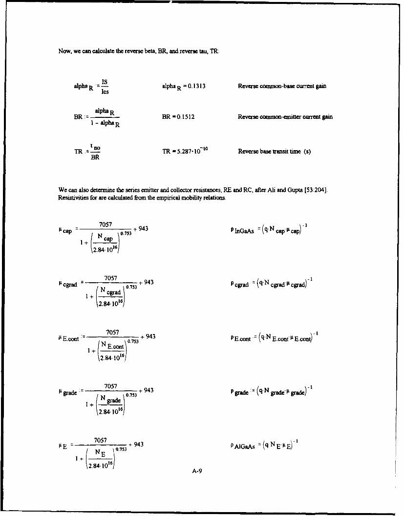
Now, we can calculate the reverse beta, BR, and reverse tau, TR:
alpha R LS - alpha R = 0. 1313 Reverse common-base cur.rent gainIcs
aihR-alphaR'Ol1 eereoRo-ascret
BR alpha R BR =0.1512 Reverse common-emitter cAre gain
I - alpha R
tioTR .=- TR = 5.287,10-'° Reverse base transit time (s)
BR
We can also determine the series emitter and collector resistances, RE and RC, after All and Gupta [53:204].Resistivities for are calculated from the empirical mobility relations.
7057 +Pi~~
R cap 0.75 +943 p InGaAs 3 (q.N cap-A cap)Ncap
ý2.84- 10 161
cgrad7057 943 P cgrad (q-N cgradI cgrad)
+ cg cgrad
2.84. 10 16!
7057 943 PE.cont (q.N E-contAE.cont)-P E.cont 0.753
IN E.cont~
2.84.1016!
7057
IL grade 705 0.753 + 943 P grade :=(q. 1 grade.'I grade)-
r 1+ (N grade0.394
2.84 1016)
7057 +943 (q.NRE + N 6ý0.75394 P AGa~sE&'E
(E- 10NE A-9
84.1016IA-9

-- -- -"'
705707-5 93 pC --(q-Nc.#c)1
LsubC 7057 +943 PsubC =(q.nsubC';tsubC)"I N subC 0.753
2.84-1016/
_p 360 047+0P (q.N B.Pp)-!lip + 40 PB :
NB 0.417
P InGaAs = 3.1423. 10- Estimated resistivity of the InGaAs cap layer (ohm.cm)
P cgrad = 6.0764-1074 Resistivity of the In graded region (ohm.cm)
P E.cont = 0.0012 Resistivity of the continuous GaAs region (ohm.cm)
P grade = 0.0075 Resistivity of the Al graded region (ohm.cm)
P AIGaAs = 0.0075 Estimated resititvity of the AIGaAs emitter region (ohm cm)
PB =0.0017 Resistivity of the p-type GaAs base (ohm.cm)
P C = 0.0632 Resistivity of the n-type GaAs collector (ohm.cm)
P subC = 0.0018 Resistivity of the n+ GaAs subcollector (ohm.cm)
PEI =PhnGaAs"1 cap + (Pcgrad) I cgrad - P E.cont'I E.cont
PE2 =(Pgrade)' grade+ PAGaAs ( wide -X IA
A-1 0
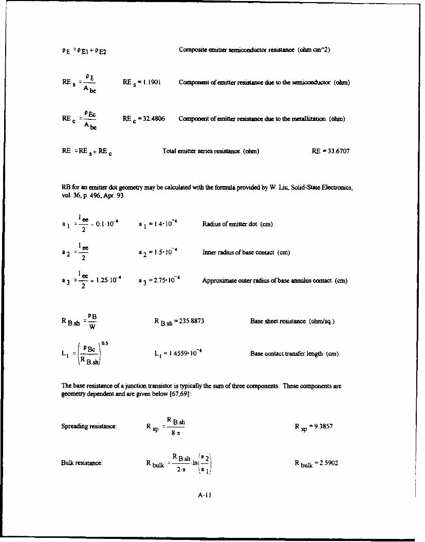
PE PEI + PE2 Composite emitter semiconductor resistance (ohm.cmA2)
= RE = 1.1901 Componentof emitter resistance due to the semiconductor (ohm)A~ Abe
REC = RE c =32.4806 Component of emitter resistance due to the metallization (ohm)A be
RE RE +REC Total emitter series resistance (ohm) RE = 33.6707
RB for an emitter dot geometry may be calculated with the formula provided by W. Liu, Solid-State Electronics,vol. 36. p. 496, Apr. 93.
ee 0.1-10. 4 a I = 1.4"104 Radius ofemitter dot (cm)2
Icee- a 2 = 1.5-10-4 Inner radius of base contact (cm)2
a3 =- + 1.25-1074 a 3 =2.75 10-4 Approximate outer radius of base annulus contact (cm)2
R B.sh WPB R B.sh = 235.8873 Base sheet resistance (ohm/sq.)
I 0.5
L t = Lt = 1.4559- 10-4 Base contact transfer length (cm)R B sh/
The base resistance of a junction transistor is typically the sum of three components. These components aregeometry dependent and are given below [67,691:
RB~shSpreading resistance: R sp 8.R sp = 93857
R B~sh 8Bulk resistance: Rbulk -2. Ian Rbu= 2 .9 02
A-1 I

R BK' I .1 1L t a ,t -K O L tLateral contact resistance: R Ic = R - L L t L (t ).t ( )
R ic = 31.3088 t (t) ýi).KL(t
Total base series resistance (ohm): RB T RI RB T = 43.2846N dotN fin
However, for S-parameter analysis, the base-collector capacitance is distributed across the base resistance.The base resistanre is split into two elements: RB and RBext.
R sp R bulk + R IcRB:: s RBet-
N dot' N fin N dotN fin
The capacitance of the base metal-semiconductor contact is in parallel with RBext. However, due to the highbase doping the barrier is very thin and there is essentially no SCR. Tunneling current occurs easily; thusCbcon can be neglected.
The collector resistance is also comprised of spreading, bulk, and lateral contact resistances. When thetransistor is operated in the active region (as is the case for microwave operation), the collector layer is fullydepleted and does not contribute to the series resistance. However, better agreement on the I-Vcharacteristics is obtained when the resistance of the collector layer is considered. When the transistor issaturated, almost the entire collector region is resistive.
PC"(1C-X 40 ) R C = 4 8 .2 9 8 1 Zero-bias collector series resistance (ohm)RC- 2
1 ee.N dot
R subC.sh PubC R subC.sh = 18.1238 Subcollector sheet resistance (ohm/sq.)
I subC
Pc 0.5L t = R bCsh L t = 3.32191F Collctor contact transfer length (cm)
A-12

Since the collector current enters the subcollector layer through an area approximately 3x3 microns square (theemitter dot), and then follows two parallel paths, we have:
Spreading resistance: R R sp 3 Rsp .6.0413SP 3
1 bc+ 1ebBulk resistance: Rb lk I .-(R ) -n bulk - 8.8305
Lateral contact resistance: RIc R sC L c coth , R c - 5.522I cc (l)t
The total ac collector series resistance ihay be assumed different than the dc resistance as given by thefollowing expressions:
RC ac _ R sp R bulk + R Ic RC ac = 20.3938
RCdc R sp RbulkRlc C RCdc=68.6919
The two remaining dc model parameters are ISE and ISC, the recombination diodes saturation currents. Theseparameters can be estimated by calculating a composite reembination saturation current that is the sum of allthe individual recombination component saturation currents. ISE is the constant for the Vbe exponent andISC is the constant for the Vbc exponent. The analytical expressions for the recombination currentcomponents are found in Ryum and Abdel-Motaleb [45], Liou [52], and Huang and Abdel-Motaleb [661.
The bulk base recombination saturation current expression comes from reference [45], with the exception thatthe drifi-difftision model is used to determine the base-emitter carrier concentrations.
ISE BR~ : N 1 oh1 B l.ihl) ISE BR =4.771 l10-35t no'N B / L / / \LnB
A-13

LSC BR tun!B _ I ISC BR = 4 .7711 I.
The SCR recombination saturation currts from reference [661:
q- A r n iE + nic 1ISESCR niE.(l wide- XG) + XG÷niB.X2oI ISE SCR = 7.4788- 1
2 .t SRH 2
ISCS -- (n.X 3 o÷nicX 4) ISC SCR = 1.39970-172.t SRH SSC
The surface recombination saturation current from reference [45]:
ISE SR = qP.S o0 L s-niB ISE SR = 55212"10-
The sum of these individual components are the composite saturation currents ISE and ISC:
ISE = ISE BR `ISE SCR + ISE SR ISE = 6.2691-10-I
ISC := ISC BR + ISC SCR ISC = 1.3997"106-
The final dc model parameter is the forward knee current which models the degradation of beta at highcurrents.
IKF = q.A be-N c-V sat IKF =0.002
Since for this device the collector metal surrounds the base finger, the parasitic base-collectorcapacitance, Cbcp, may be calculated as follows:
r(64- 1-4+I +I..A). 1 1 405 [ 64.04+1bc+4810-)1bc 0.5[(ee*0.5 +1bc).(64.10-4+ Ibc)] 0(4.10-4 + 1be)(48. 10- + I b)]
A- 14
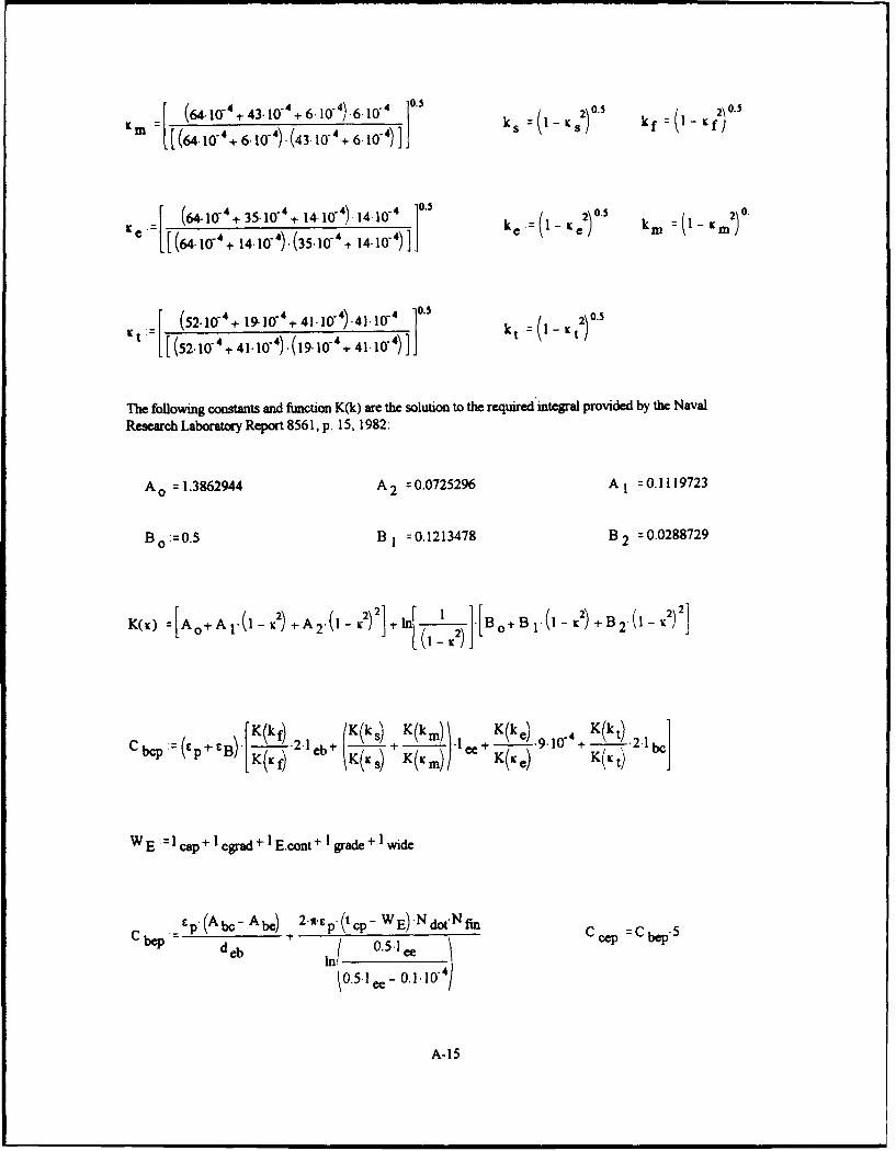
f (64,10,4 +43. 104 +6- 1o-4 )6. 10'4 0j ( S)- k
([64,10-4+6.104) -(43-10-4+6.10'] 4K) 1k f (i-K)1•0.5•[2 .
e (64.1()74+35. 10-4+ 14-1l0-4).14. 10-' (i5 e _ r 2) 0.5 2)- KK (6 .o-4-+ 141074).(35.•10-- 140-4) 14.1
ft (52. 1074 + 19.1i-4 + 41. 1074).41. 10-4 10.5k Kt203
The following constants and function K(k) are the solution to the required integral provided by the NavalResearch Laboratoiy Report 8561, p. 15, 1982:
A 0 = 1.3862944 A 2 = 0.0725296 A1 =0.1119723
Bo:=0.5 B 1 =0.1213478 B 2 =0.0288729
K(K) 4A0 +.sA(I - K2) -+A2'(' - I + ]n[ K[2) ]l B 0+B i.(I - K2) +B 2 -(1 -K)
Che (+p B) [(kf). 2-1 b± (K(k:S) + 7(krn) + C) .1 +~ 9. 10-4 + Kk) -2.1b
WE =Icap+ I cgradt + E.cont+ I grade + 1 wide
p P(Abc- Abe) 2"'-cP'(tcp- WE).NdOt'Nfi C cep =Ebe'5decb In 0.5-1 ee )
0.5-1 ee- 0.1.10-4
A-15

That is also an mductawe associtated with each terminal of the tmmastor The equatIoa for estimating thisinductance is given by Ladbrooke [59:99]:
13 4.5 9 7.5 10
p+ + Lbp :o(tsub2 -1 +0 15 1
L 0:$t. d b. l'e- +lb I bee)
ep I bb 2-1eb1
The resistance in series with each inductance can be calculated from Ladbrooke [59:1461:
R cp-= -c4 R cp =0.03153 ."t p lIcc + 4.5. 10"4
Rbp= -u.( e+ Tee) R bp= 0.0427Rp 3. tcp 1 bb 2"feb/
The following are six parasitic equivalent circuit elements that are external to the SPICE BJT model:
C bep =3.382810-15 The parasitic interelectrode base-collector capacitcance (F)
C bep = 1.148 10-15 The parasitic interelectrode base-emitter capacit-nce (F)
Ccep= 5.7403"106-l The parasitic irterelectrode collector-emitter capacitance (F)
Lcp = 1.5554" 10-10 The parasitic collector inductance (H)
L bp = 1 9059. 10- The parasitic base inductance (H)
L ep = 2.6389 1012 The parasitic emitter inductance (H)
A-16

All of the calculated SPICE model parameters aie summarized below for the 3 micron mutter. 1 dot geoameuy.
BF = 83.5413 Forward common-emitter current gain
BR = 0. 1512 Reverse common-emitter current gain
TF = 9.5681-10-3 Forward base transit time (s)
TR = 5.287 10-10 Reverse base transit time (s)
IS - 2.2354-O16-" Transport saturation current (A)
ISE = 6.2691" 10-9 Bcse-emiter leakage saturation current (A)
ISC = 1.3997-10-7 Base-collector leakage saturation current (A)
RE = 33.6707 Emitter series resistance (ohm)
RB = 9.3857 Intrinsic base series resistance (ohm)
RB T = 43.2846 Total base series resistance (ohm)
RC ac = 20.3938 Microwave collector series resistance (ohm)
RC dc = 68.6919 DC collector series resistance (ohm)
CJE = 9.8515-10-15 Base-emitter zero-bias depletion capacitance (F)
CJC = 1. 119_ 10-4 Base-collector zero-bias depletion capacitance (F)
VWE = 1.7018 Base-emitter built-in potential (V)
VJC = 1.3691 Base-collector built-in potential (V)
XCJC = 0.2053 Fraction of base-collector depletion capacitance internal to base
IKF = 0.002 Comer for high current BF roll-off (A)
The following is an equivalent circuit element that is external to the SPICE BJT model:
RB ext = 33.8989 The base contact resistance (ohm)
A-17

HBT PHYSICAL PARAMETER CALCULATIONS
Author: James A. FellowsDate: 20 Nov 93Filename: H_3uSdlf mcdDescription: This program determines all of the model parameters required to characterize a gradedAIGaAs/GaAs heterojunction bipolar transistor (HBT) in SPICE The calculated parameters will be placeddirectly into the SPICE BJT model card. Also calculated are the parasitic inductance and capacitanceequivalent circuit element values. All values are physically determined using a knowledge of only the devicematerial, geometry and fabrication process. Only three of the four ideality factors are empirically determined.Inputs: This program requires the device designer to input several specific fabrication constants. Thesevariables are included in the first section for convenience.
Fabrication Parameters:
N E = 5-101" AIGaAs emitter doping concentration (cm^-3)
NB -5.1019 GaAs base doping concentration (cm^-3)
NC =8.1015 GaAs collector doping concentration (cmA-3)
N subC =3-1018 Subcollector doping concentration (cm^-3)
1 cap = 3.10- 6 Thickness of InGaAs emitter cap (cm)
N cap =2. 10 19 Cap doping concentration (cmA-3)
-cgrad := 2.5-10"6 Thickness of lnGaAs graded region (cm)
N cgrad =I .10 19 Graded region doping concentration (cmA-3)
1 E.cont = 1.0- '5 Thickness of GaAs emitter region (cm)
N E.cont =5-1018 GaAs doping concentration (cmA-3)
1 grade = 5. 10-6 Thickness of AIGaAs graded region (cm)
N grade = 5.1017 AlGaAs graded doping concentration (cmA-3)
1 wide = 5. 10- 6 Thickness of the AIGaAs emitter (cm)
X G 61.5-0- Thickness of emitter-base junction grading (cm)
A-19

W -7.107f Thickness ofthel•Ga s base (an)
IC := 1.10-4 Thickness of the GaAs collector (cm)
1 subC ý= " 10-4 Thickness of the GaAs subcollector (cm)
I Ce:=3.10-4 Diameter ofan emitter dot (cm)
N dot:=5 Number of emitter dots/finger
N fin:= I Number of base-emitter fingers
I cc 2.N dot-I ce The length ofthe collector contact (cm)
I c= 18.75. 10-4 The width of the collector contact (cm)
I eb 1"10"4 The width of base finger contact on either side of emitter dot (cm)
1 bC:= 1.10-4 The lateral distance between the base and collector contact (cm)
PEc = 2. 10-6 Estimated emitter specific contact resistance (ohmncm^2)
Pik, = 5.10-6 Estimated base specific contact resistance (ohm.cm^2)
Abe:_N dot.Nfin. (2-O.l-)0-)
Abe =3.0788-10 - Base-emitter junction area (cmA2)
Abe :=N dot.N fin-(lee + 2.10"4).(I ee-2)
Abc = 1.5. 10-6 Base-collector junction area (cm^2)
XCJC Fraction of base-collector area intermal to device
Abc
P :=N f.N dot'" 2 -0.1- I0" Total perimeter of emitter-base junction (cm)
A-20

d eb :: 1. 10" 4 Height of polyimide between the base and emittermetallizations (cM)
top :0.4.10-4 Thickness of collector pad metal (cm)
Ibb Ilee+ 2.10'4 Width ofbase finger (cm)
t ub-70-1074 Thickness of GaAs substrate (cm)
I c 3110-4 Thickness of polyimide between the collector pad ad theemitter bridge (cm)
"A CP 9.63. 10'6 Area of thick collector pad under emitter bridge (cm^2)
"Acm = 13.6925.10- 6 Area of entire collector under emitter bridge (cm^2)
General constants:
k := 8.61738.10- Boltzmann's constant (eV/K)
q := 1.602.10-19 Electron charge (C)
co :=8.854.10.14 Permittivity in vacuum (F/cm)
ito :=4.x. 10-9 Permeability in vacuum (H/cm)
mo:=9.1095. 0- 31 Electron rest mass (Kg)
T :=300 Temperature (K)
Material constants:
The only user defined constant is x, the mole fraction of Al. The expressions below are taken from thefollowing references [24, 55, 57, 59].
x := 0.35 Mole fraction of Al in the emitter
E gE 1.424 + 1.247.x Band-gap energy of the AIGaAs emitter (eV)
I
AE = 1.6.10-'.N B3 Band-gap shrinkage in the GaAs base (eV)
A-21

E g: := 1.424 - AE gB Band-gap ergy of the GaAs bawe (eV)
AE :=EE- EgB Band-gap differemce at the abrupt emitter-base heterqjunction(eV)
c:= 13.18- 3.12.x Relative pernittivity of the AIGnAs emitter
9B := 13.18.co Permittivity of the GaAs base (F/cm)
EE =6.6o Permittivity of the AlGaAs emitter (F/cm)
Cp :=3.5.to Permittivity ofpolyimide (F/cm)
n : 1.7 9 . 16.exp (---B-0 Intrinsic carrier concentration in the GaAs base at300K as akT function of doping (cmA-3)
"niE = n iB.exp -. A .0.5 Intrinsic carrier concentration in the emitter at 300K (cmA-3)
* iC : = 1.79. "' Intrinsic carrier concentration in the collector (cm^-3)
Vsat := 1. 167 Electronsaturato velocyin GaAs at300K (cm/s)
Nt :=1 150 SRH recombination trap density in GaAs (cm^-3)
NtI= 1.1012 AIGaAs/GaAs interface density of states (cmA-2)
a n := 1.10 is Capture cross section of an electron (cmA2)
m n' = 0.067. in 0 Electron effective mass in GaAs (Kg)
Ap = 1.-I0" ° Auger recombination coefficient in GaAs (cmn6/s)
B = 2.10- 10 Radiative recombination coefficient in GaAs (cmA3/s)
"P Au = 2.44. 106 Resistivity of gold metallization (omn.cm)
AEc := 0.797.x Difference in conduction band energy at the interface (eV)
So =I.106 Intrinsic surface recombination velocity (cm/s)
L 1= 1.10" Surface diffusion length (cm)
A-22

One of the most elementary calculations is that of the built-in voltage for each junction:
VJE :k.T.ln( + AEN _ VJE - 1.7018•niE.n iB/ 2
vic :=k-T-n N B-NC) VJC -1.3454\niB'n ic)
The zero-bias depletion widths may be calculated from Ryum and Abdel-Motaleb [23:873]:
,-/2-NB_.E-EB.(VJE- .64.k.T) NEso q.NE.(E.NE- -B.NB) No NB
x J2.NC-E B' (VJC -k- T) N
q.NB.(NC+NB) 40 'NC
"X lo 6.6288" 107 On the emitter side of the EB junction (cm)
" 2o - 6.6288-107' On the base side of the EB junction (cm)
"X 3o 7.8426 1079 On the base side of the CB junction (cm)
X 40 = 4.9016" 160 On the collector side of the CB junction (cm)
The effective zero-bias base width Wb, is found by subtracting the depletion widths in the base on both theemitter and collector sides:
WB :=W- (X 2 o+ X3o) WB =-6.9259"10- (cm)
Now, calculate the depletion capacitances from Ryum and Abdel-Motaleb [23:873]:
A-23

CJE =Abe. (2E'oB) CJE -4.9257-10SE'X 2o+ CB'X 1o
CJC:Abcx 9 CJC =3.5706"01-14X 3o + X 4o
Calculating the value of Cje with a nominal bias is helpful. Since a nominal value of Vbe is 1.5 V, we have:
2 .NB.CE-CB.(VJE- 1.64.k.T- 1.5) NEx to:=X~o ý--.X o
l j q.NE.(CE.NE ECB.NB) NB
CJE bias A be (CE.B) CJE bias = 1.5895.10-13
CE"X 2o0+ rBX 1o
The minority elecfton mobility in the p-type base GaAs as a function of base doping can be found fromthe empirical relation stated by Ali and Gupta [53:202]. A similar relation for minority holes in thecollector is stated by C. Selvakumar [55:773]. The diffusivities are then calculated from the Einsteinrelation:
7057n- 07 943 Jn = 9 6 8 .29 7 9 DnB =An~k-T
1+1 NB 0
2.84-1016/
360JipE i- 40 = E 9 4 6 8 DpE IPpEk.T30 0.417 40iL pE =194.1658 p =pEk-
360PpC:= o.417 ±40 iLpC = 330.7 825 D PC =IpC.k.T
+
A-24

"D nB = 25.0326 Diffusivity of minority electrons in the base (cm^2/s)
"D pE - 5.0196 Estimated diffusivity of minority holes in the emitter (cm^2/s)
"D pc = 8.5514 Diffusivity of minority holes in the collector (cin^2/s)
The base transit time has many forms [60,51], but ultimately from from Hodges and Jackson [44:162]:
= W 2 W 2 W B_ W 2
2.43.D nB 2-DnB vsat 2"DnB
"TF = 9.5811.10-13 The forward transit time of minority electrons across the base (s)
Excess minority electron lifetime may be obtained by considering the lifetime of each recombinationcomponent. The expression for mo is taken from Lundstrom et al. [56:6981:
vth q-kT 0 5 Vth = . 0 3 9 2-I0l Average thermal velocity of an elecron in GaAs (cm/s)
t SRH:- a tSRII = 9.6227.610 Shockley-Read-Hall recombination lifetime in GaAs (s)on'Nt-Vth
1 410-
tAug -Ap.NB2 t Aug 14 0 Auger recombination lifetime in p-type GaAs (s)
trad I t rad = 1-106-l Radiative recombination lifetime in p-type GaAs (s)
tB-N B
tO tSRH t Aug t /
A-25

t no 7. Minority electron hfeume in the bre (s)
ti = 2& iOr Minority hole hfietie in the collector (s)
gni, TD 't. L B = 4.4732" 16' Difftion length of electrons m the base (cm)
LLC:=ID .tC Lp =4.1356'10 Difi-sion length of holes in the colector (cm)
The diffusion length of minority holes in the emitter is estimated from an emirical expression found m Ryumand Abdel-Motaleb [23:876]:
42.46 - log(N E)LpE = - lo2-N L pE = 0.0027 Diffusion length of holes in the enitter (cm)LpE- ~9.21.0
The maximum dc Beta for an HBT is best described by Kroeme [1 3:15]; however, better dc agreementbetween modeled and measured data is obtained if beta is conmdered due only to recombination in theneutral base after Grossman and Choma [25:459]:
DBDpE NEVnB (k.\TV DB VpE -D BFmax N E v p
LnB LpE NB VpE
tn
BF - BF = 83.4288TF
IS can be estimated from Huang and Abdel-Motaleb [66:1651:
2I-q-Abe~niB2.D nBIS 116962-IS =.~n~ IS =I. ll!69" 0-2'
WB.NB
2 2Ics =Abe..( LnBNiB DLpcn iC Ics =2.0744-16-N
A-26

Now, we can calculate the reverse beta, BR, and reverse tau, TR:
Isalpha R : alpha R - 0.0538 Reverse common-base current gain
BR R- BR = 0.0569 Reverse common-emitter current gain
1 - alpha R
TR -!no TR = 1.4046-1079 Reverse base trsit time (s)BR
We can also determine the series emitter and collector resistances, RE and RC, after Ali and Gupta [53:204].Resistivities for are calculated from the empirical mobility relations.
Icap = 7057 0.7531t943 plnG&s = (q.N cap. AW)
I cap °s
\2.s4- 10"6/
Itcgrad 7057 0.753 t 943 P cgrad (q.N cgradAcgrad)(N cgrad'\
2.84* 101!
E.cont N7057 0.753 +943 P E.cont (q.N E.coatP E.cont)I NExcont\(2.84-1016!
7057 -5ade7 - 943 Pgrade "q- N grade- N grade),
1+ grades
2.84-1016/
= 7057 0-75
P 705 0.5 943 p AlGaAs :=, (q-N E' A E
+2 .84-10 16A-27

C 70:: + 943 PC (q-N C' ,C)
7057 )IA sUbC 43 suC (q'N bC-IbC
1 2.84.10'I .S
"•p + ( 60 0) 417 40 PB := ( q 'N B 'L p
p InGsus = 3.1423 -10' Estimated resistivity of the Inh•As cap layer (ohm.cm)
p ograd = 6.0764- 10' Resistivity of the In graded region (ohm.cm)
P Exont =0.0012 Resistivity of the continus GaAs region (ohn.cm)
p grade -0.0075 Resistivity of the Al graded region (ohm.cm)
p AIGaAs = 0.0075 Estimated resititvity of the AIGaAs emitter region (ohm.cmn)
PB = 0.0017 Resistivity of the p-type GaAs base (ohm.cm)
PC= 0.1292 Resistivity of the n-type GaAs collector (ohm.cm)
P subC -0.0018 Resistivity of the n+ GaAs subcollector (ohm.cm)
PHI := P InGaAs"1 cap + (P cgrad).1 cgrad+ PE.conft"E.cont
PE2:= (P grade)I grade +P AIGaAs (I wide- X Io)
A-28

PE ý=PEI PE2 Composite emitter semiconductor resistance (ohmcm^2)
PEREs A beRE s = 0.238 Component of emitter resistance due to the semiconductor (ohm)
Abe
R PEc RE c = 64961 Component of emitter resistance due to the metallization (ohm)Abe
RE RE s + RE c Total emitter series resistance (ohm) RE =6.7341
RB for an emitter dot geometry may be calculated with the formula provided by W. Liu, Solid-State Electronics,vol. 36, p. 496, Apr. 93.
a1 - 0.1.I0"4 a =1.4-I04 Radiusofemitter dot (cm)2
a - a 2 = 1.5" 10-4 Inner radius of base contact (cm)
2lee
a3 1 1.25.10"4 a 3 =2.75"10-4 Approximate outer radius ofbase annulus contact (cm)2
R B.sh -B R B.sh = 235.8873 Base sheet resistance (ohm/sq.)W
Lt = B L t = 1.4559-10-4 Base contact transfer length (cm)
The base resistance of a junction transistor is typically the sum of three components. These components aregeometry dependent and are given below [67,691:
Spreading resistance: R sp = R sp = 9.3857
Bulk resistance: Rbulk - I( bul 9
A-29

RBRshLtl Lt/ La t ~ Lt LtLateral contact resistance: R Ic - (.()
21a 2 I KKI - t] k -t/
R Ic = 31.3088 Lt/
Total base series resistance (ohm): RBT RSP+Rbu+Rlc RB T = 8.6569N dot-N fin
However, for S-parameter analysis, the base-collector capacitance is distributed across the base resistance.The base resistance is split into two elements: RB and RBext.
RB: R sp RBext R bulk + R ic
Ndot.Nfin N dot.N fin
The capacitance of the base metal-semiconductor contact is in parallel with RBext. However, due to the highbase doping the barrier is very thin and there is essentially no SCR. Tunneling current occurs easily, thusCbcon can be neglectew.
The collector resistance is also comprised of spreading, bulk, and lateral contact resistances. When thetransistor is operated in the active region (as is the case for microwave operation), the collector layer is fullydepleted and does not contribute to the series resistance. However, better agreement on the I-Vcharacteristics is obtained when the resistance of the collector layer is considered. When the transistor issaturated, almost the entire collector region is resistive.
RC -PC('C-X4o) R c = 14.6421 Zero-bias collector series resistance (ohm)21 ee .N dot
RsubC.sh - P subC R subC.sh = 18.1238 Subcollector sheet resistance (ohm/sq.)1 subC
0.5
L t sPEc Lt = 3.3219 10-4 Collector contact transfer length (cm)R subC.shA
A-30

Since the collector current enters the subcollector layer through an area approximately 3x3 microns square (theemitter dot), and then follows two parallel paths, we have:
Spreading resistance: R R subC.sh R sp = 0.3021sp 12. N dot
Bulk resistance: Rbulk =I ee2N dot n(2). (R subC.bh) R bulk -0.8375
R subC'sh Ltct ' l c=103Lateral contact resistance: R Ic - R u ch L tcoth ) 1.0035
The total ac collector series resistance may be assumed different than the dc resistance as given by thefollowing expressions:
RC ac R= R bult+RIc RC ac = 2.143Nfm
R tR tlkRIC
RCdc- sp Nbu f IcRC RC dc = 16.7 8 5 1
The two remaining dc model parameters are ISE and ISC, the recombination diodes saturation currents. Theseparameters can be estimated by calculating a composite recombination saturation current that is the sum of allthe individual recombination component saturation currents. ISE is the constant for the Vbe exponent andISC is the constant for the Vbc exponent. The analytical expressions for the recombination currentcomponents are found in Ryum and Abdel-Motaleb [45], Liou [52], and Huang and Abdel-Motaleb [66].
The bulk base recombination saturation current expression comes from reference [45], with the exception thatthe drift-diffusion model is used to determine the base-emitter carrier concentrations.
qAeLnB.niBI oh 1 / WB sn 'B W -34ISEBRcs- - ISE BR = 2 .38 7 1 -
tno'NB \L nBI L \LnB
A-31

qISB = WNB kiB. L ISCBR 2. 38711
The SCR recombination saturation currents from reference [66]:
ISESCR:=qAbe niE.(wide XG) + niEn XG niB'X2o ISESCR =-3 .7 3 9 4 "10-19
22.t SRH 2
ACR bc (niB'X 3o+n iCX4o) ISC SCR = 1.0961"10-16ISC CR 2- 2t SRH
The surface recombination saturation current from reference [45]:
ISE SR q'P" S 6.L s.n jB ISE SR = 2.7606-10-
The sum of these individual components are the composite saturation currents ISE and ISC:
ISE ISE BR + ISE SCR + ISE SR ISE = 3.1345-10-8
ISC =ISC BR I+SC SCR ISC = 1.0961"10-16
The final dc model parameter is the forward knee current which models the degradation of beta at highcurrents.
IKF = q.A beN c.Vsat IKF = 0.0039
Since for this device the collector metal surrounds the base finger, the parasitic base-collectorcapacitance, Cbcp, may be calculated as follows:
[(lei+ Ibce7)Ic~ 1 f(cl+lbe+lbb)]be] ]0.5 kS2A5[QscIe+lbq(cl+ebý)l K0* i j [ Ib b)'(I Ilb)] k5s (
A-32

f L(Icc+ 45-,1' +,1b+ 53,o,-) b,•] 10o,0
(Icc+ 0.I 4+ 4-104+ 5-10 4.3410 41'k~ = (1.2) 05 k
xo C (Icc+ 50o. 14+ 34,o0.) -(34, 1,o4+ 15.10-4)] kC- ,€
K Ic 0 04 .. 04+ 51-4 .- 0 10.5 kt z(1 .,2) 0.
(I[ (c +" 60. 10'+ 8.5. 1 +35104) k
The following constants and function K(k) are the solution to the required integral provided by the NavalResearch Laboratory Report 8561, p. 15, 1982:
Ao = 1.3862944 A 2 =0.0725296 A 1 =0.1119723
Bo:=0.5 B = 0.1213478 B 2 =0.0288729
K(x):A A.l2)A.I .[B+B(- 2+B
Ii I( + B)K(k1) K(ks) K(kf) leb .Nftp(2.1cc+Ibb)
C~~~~~ ~ ~ Kc2( B ~e.2 l . -1--4 ,K•t).51-42 bcp= bcpl + C bcp2
SAcp÷AcmI
;v I 01 ( 4)1 cap +Icgrad+1Econtt 1grade+Awide
A-33

cp.[Abc- Abe (Nfi.lbb2)1 2Wxcp.(tcp WE)-NdjgCNfdeb- 0.1-10" I 5 e-
0.5-1 c- 0.1-10-'4
There is also an inductance associtated with each terminal of the transistor. The equation for estimating thisinductance is given by Ladbrooke [59:99]. Only the interconnects NOT beneath the emitte bridge (and NOTpart of the thick pad metal) are considered here since the inductance under the bridge is negligible incomparison.
Lcp- o' tsub-'t'4) L bp I o't sub.'7.5 + '
L b p l N f n 0 d et ( 0 .1 .-1 0' ) ( c + 2 ceb ) I O .( c . 0 4
I\cc + 7 .8.O 10 1 1 ~-L cpl: o(1 ec 0. 1"-10-4) -e÷ "8 I " L p :=/ + _ ._- I
(N + Icl LCpl Lbpl
The resistance in series with each inductance can be calculated from Ladbrooke [59:146]:
R = Au -[ jc÷7 "8 "I0"41 = 0.0205
Ndot PAu (lee lIe)Rbp :.t- p _ R bp =0.2135
N fi 3 -tcpIbb 21e
The following are six parasitic equivalent circuit elements that are external to the SPICE BJT model:
C bp = 1.6333" 10-14 The parasitic interelectrode base-collector capacitcance (F)
A-34

C b = 7.0116" 10-" The parasitic interelectrode base-emitter capacitance (F)
C cep M2.4922" 10-14 The parasitic interelectrode colle(.v'-emittae capacitance (F)
L cp M 2.7367- 16-1 The parasitic collector inductance (H)
Lbp = 1.9059,10-l1 The parasitic base inductance (M)
L ep = 2.9703.1012 The parasitic emitter inductance (H)
All of the calculated SPICE model parameters are summarized below for the 3 micron emitter, 5 dot one fingergeometry.
BF = 83.4288 Forward common-emitter current gain
BR = 0.0569 Reverse common-emitter current gain
TF = 9.581 1.10- 13 Forward base transit time (s)
TR = 1.4046- 107' Reverse base transit time (s)
IS = 1.1169.1062' Transport saturation current (A)
ISE = 3.1345- 106- Base-emitter leakage saturation current (A)
ISC = 1.0961.10-16 Base-collector leakage saturation current (A)
RE = 6.7341 Emitter series resistance (ohm)
RB = 1.8771 Intrinsic base series resistance (ohm)
RB T = 8.6569 Total base series resistance (ohm)
RC ac = 2.143 Microwave collector series resistance (ohm)
RC dc = 16.7851 DC collector series resistance (ohm)
CJE = 4.9257 10-14 Base-emitter zero-bias depletion capacitance (F)
A-35

CJC - 3.5706- 10-1 Base-collector zeo-bias depletion capacitance (F)
VJE - 1.7018 Base-emitter built-in potential (V)
VJC - 1.3454 Base-collector built-in potential (V)
XCJC = 0.2053 Fraction of base-collector depletion capacitance internal to base
WKF = 0.0039 Corner for high current BF roll-off (A)
The following is an equivalent circuit element that is external to the SPICE BJT model:
RB ext = 6.7798 The base contact resistance (ohm)
A-36
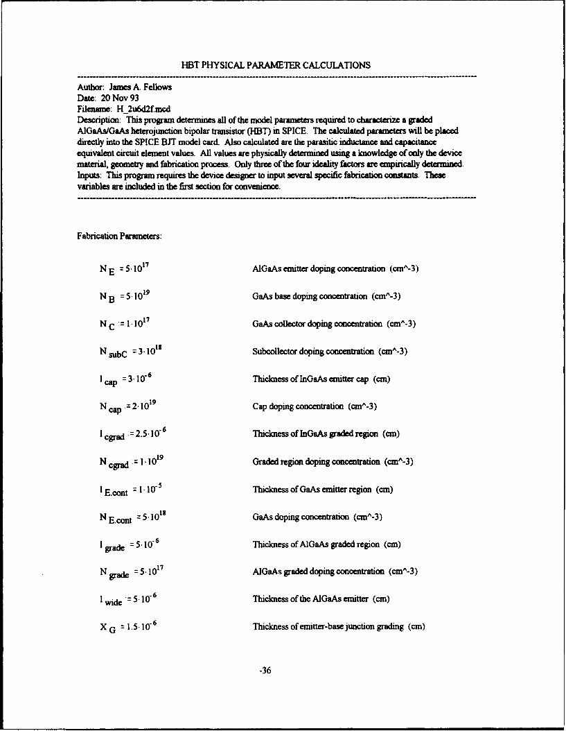
HBT PHYSICAL PARAMETER CALCULATIONS
Author: James A. FellowsDate: 20 Nov 93Filename: H_2u6d2fmcdDescription: This program determines all of the model parameters required to characterize a gradedAlGaAs/GaAs heterojunction bipolar transistor (HBT) in SPICE. The calculated parameters will be placeddirectly into the SPICE BJT model card. Also calculated are the parasitic inductance and capacitanceequivalent circuit element values. All values are physically determined using a knowledge of only the devicematerial, geometry and fabrication process. Only three of the four ideality factors are empirically determined.Inputs: This program requires the device designer to input several specific fabrication constants. Thesevariables are included in the first section for convenience.
Fabrication Parameters:
N E 5.1017 AlGaAs emitter doping concentration (cm^-3)
N B = 5.1019 GaAs base doping concentration (cm^-3)
N C 1.1017 GaAs collector doping concentration (cra^-3)
N subC 3. lois Subcollector doping concentration (cmA-3)
lcap .= 3-10.6 Thickness of InGaAs emitter cap (cm)
N cap :=2.1019 Cap doping concentration (cmA-3)
I cgrad : 2.5. 10.6 Thickness of InGaAs graded region (cm)
N cgrad := I. 1019 Graded region doping concentration (cm^-3)
I Econt =I -1. 0" Thickness of GaAs emitter region (cm)
N E.cont =5.10oi GaAs doping concentration (cmA-3)
1 grade = 5 .10 6 Thickness of AIGaAs graded region (cm)
N grade = 5. 10 i7 AlGaAs graded doping concentration (cm-3)
I wide =5.10.6 Thickness of the AlGaAs emitter (cm)
X G =1.5-10-6 Thickness of emitter-base junction grading (cm)
-36

W :=7.10' Thicknesod GaAs baen (ca)
Ic :=0.35. 1ff4 Thickness oftheGAO1s cC(eor (cm)
1 subC -hicnes4 colthe GaAs subcolector (cm)
I =210 Diameter of an emitter dot (cm)
N dot :6 Number of emitter dots/finger
N fr:=2 Number of bae-emitter fingers
I c =2.N dot.I e The length of the colector contact (cm)
1I C= 19.55-10"4 The width of the collector conwtac (cm)
1 eb = 1. 04 The width of base finger contact on either side of emitter (cm)
I bc= 1"10"4 The lateral distance between the base and collector contact (cm)
pEc = 2. 106 Estimated emitter specific contact resistance (ohm.ncm2)
PBc :=5'10'6 Estimated base specific contact resistnce (ohm.cma2)
Abe:=N .Nd -a.( - 0.1.10)
A be =3.0536-16' Base-emitterjunction area (cm^2)
Abe:= N do(-Nfln. (l + 210- 4). (I -2)
Abe = 1.92-10- Base-colecto unction ar• (cmA2)
XCJC be Fraction of base-collector area internal to device
A b
P:=NrfmNdot. -0.1-10" Total perimeter of emitter-base junction (cm)
A-37

deb •11 4 Height of polyimide between t bas and emiter
metallizations (ca,)
tp C=0.4.10'4 Thickness of collctor pad meal (cm)
I bb= I=ew+ 2.1ITf4 Widthofbae finger (ca)
tsub :=70.I0"4 Thickess oftGArs susrate (cm)
lec:=3.10'4 Thickness of polyimide between the collector pad and theemitter bridge (cm)
"A = 12.972.1Cf 6 Area of thick collector pad under emntter bridge (cmA2)
"Ancm 18.555.1ff'6 Area ofentire aofectr under emitter bridge (aMA2)
General constants:
k =8.61738. 1OU Boltzmann's constant (eV/K)
q :1.602.10'19 Electron charge (C)
o 0= 8.854-10' Permittivity in vacuum (F/cm)
A o: 4-s. 10f9 Permeability in vacuum (H/cm)
mo =9.1095.10-31 Elecronrest mass (Kg)
T:=300 Temperature (K)
Material constants:
The only user defined constant is x, the mole fraction of Al. The expressions below are taken fromrefeaences [24, 55, 57, 59].
x ý=0.35 Mole fraction of Al in the emitter
E 8E: 1.424 + 1.247.x Band-gap energy of the AlGaAs emitter (eV)
I
AE gB =1.6.10"r.N B3 Band-gap shrinkage in the GaAs base (eV)
A-38

E gB 1.424- AE gB Band-goa'eegy of ie GaAs banse (eV)
AE E EgB Bad-gapdip erence at the abrupt emiuer-be heerojuwcton(eV)
z:= 13.18- 3.12.x Relative permittivity of the AIG&As emitter
8B =13.18.to Permittivity of the GaAs base (F/cm)
9 E .=C-o Permittivity of the AIGaAs emitter (F/cm)
ep := 3.5.co Permittivity of polyimide (F/cm)
njB =1.79.10exp .•_O' Intrinsic carrier concentration in the GaAs base at 300K as akT function of doping (cmA-3)
niE = niBecx ý-E--) Intrinsic carrier concentration in the emitter at 300K (cm^-3)
niC 1.79.10 Intrinsic carrier concentration in the collector (cM^ -3)
v set 1- 10 7 Electo satuaton velocity in GaAs at 300K (cm/s)
Nt =1.1015 SRH recombination trap density in GaAs (cm^-3)
N tl 1.1012 AIGnAs/GaAs interface density of states (cmA-2)
an =1.I07" Capture cross section of an electron (cmA2)
mn =0.067-mo Electron effective mass in GaAs (Kg)
Ap I--10-o 3 Auger recombination coefficient in GaAs (cmA6/s)
B 2= 2-10"t° Radiative recombination coefficient in GaAs (cm^3/s)
P Au = 2.44. 10-6 Resistivity of gold mmetllization (ohm.cm)
AEc =0.797.x Difference in conduction band energy at the interface (eV)
So = I.10 Intrinsic surface recombination velocity (cm/s)
Ls =.10"'5 Surface diffusion length (cm)
A-39

One of the moat Clemntary calculatios is that of the built-in voltage for each junction:
VE =k.T.IDnN EN +AcAE WE -1.7018(niE'niB/ 2 I ,171
VJC :=k-T.lnIN B'N Cj VJC - 1.4107\niB-"nic/
The zero-bias depletion widths may be calculated from Ryum and Abdel-Motaleb [23:873]:
:: 2.NB.SE.CB.(VJE- 1.64.k.T) NEo q.NE.(EE.NEIB.NB) o NB
=2.Nc.CB.(VJC- k.T)
30o ••.lB- X4o =NB'XNC 30
q.NB.(Nc+NB) N4 C- 3
X 10 -6.6288"10-6 On the emitter side of the EB juncton (on)
* 20 -6.6288" 106 On the base side of the EB junction (cm)
* 3o - 2.8379. 1-8 On the base side of the CB junction (cm)
X 40 = 1.419-107' On the collector side ofthe CBjunction (cm)
The effective zero-bias base width Wb, is found by subtracting the depletion widths in the base on both theemitter and collector sides:
WB =W- (X2o+X 3 o) WB = 6.9053.16-6 (cm)
Now, calculate the depletion capacitances from Ryum and Abdel-Motaleb [23:873]:
A-40
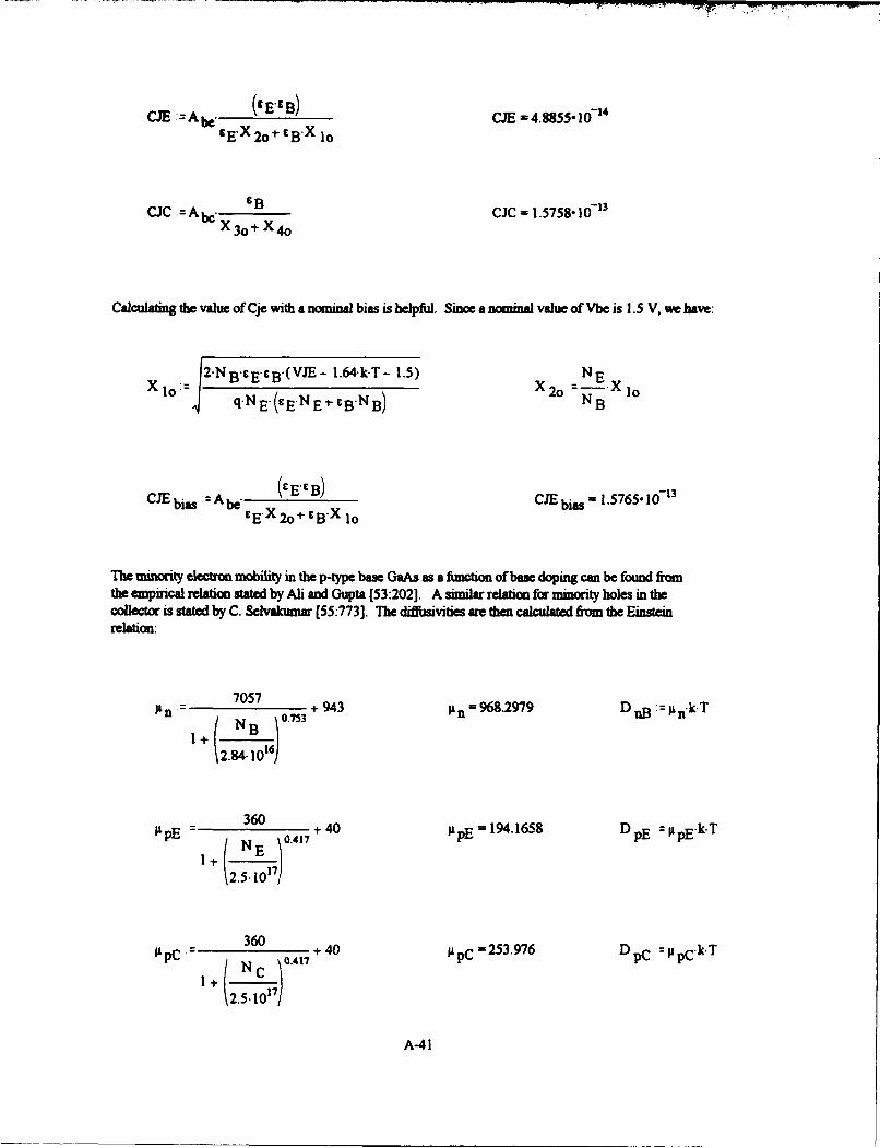
CJE:-,,.• (6E"9B) CE - 4.8855- 1o-4
60~ 2o, +1B'X lo
CJCB:=Abhe CJC - 1.5758-16-OX 3o+ X4o
Calculating the value of Cje with a nominal bias is helpful. Since a nominal value of Vbe is 1.5 V, we have:
2-NB.CE.CB.(VJE- 1.64.k.T- 1.5) NEX 10 := q.NE.(EE.NEtECB'NB) X 2o =NEB 1o
CJE bias AEbe* (.EEB) CJE bias - 1.5765.10-13cE'X 2o"+1 CB*X lo,
The minority electron mobility in the p-type base GaAs as a function of base doping can be found fromthe empirical relation stated by Ali and Gupta [53:202]. A similar relation for minority holes in thecollector is stated by C. Selvakumar (55:773]. The diffusivities are thena calculated from the Einsteinrelation:
7057AL n - 0.753 +943 1i n = 968.2979 D nB A nak*T
1+ N NB
2.84101;)
360
IpE360 0.1 +40 .L pE=l 9 4 .1658 DpE.-IL pE-k-T
360tpC 340 =pC =2 5 3 .9 7 6 DpC =ppC'k'T
A-41

"D nB- 25.0326 Diffusivity of minority electrons in the ease (cm^2/s)
"D pE =5.0196 Estimated diffusivity of minority holes in the m ,tt," (cm^2/s)
"D pC = 6.5658 Diffusivity of minority holes mn the collector (cmA2/s)
The base transit time has many forms [60,51], but ultimately from from Hodges and Jackson [44:162]:
W B2 WB 2 W B W B2
TF: TF= TF2.43.D nB 2.D nB v sat 2.D nB
TF = 9.5243-10-1 The forward transit time of minority electrons across the base (s)
Excess minority electron lifetime may be obtained by considering the lifetime of each recombinationcomponent. The expression for tno is taken from Lundstrom et al. [56:698]:
vth"=100( q-kT) 0 .5 Vth = 1.0392-106 Average thermal velocity of an electrw in GaAs (cm/s)
tSRH a t SRH = 9.6227-10-8 Shockley-Read-Hall recombination lifetime in GaAs (s)on'Nt'Vth
1 t Aug =4"I0-t° Auger recombination lifetime in p-type GaAs (s)t Aug :
Ap.NB2
trad 1 trad = 1"l0b-0 Radiative recombination lifetime in p-type GaAs (s)B.NB
t no+ (tSRH tAug trad/
A-42

trno =7.9934-106- Minornty •.lccu lift in the base (s)
t poc 20 10'9 Minority hole lifetime in the collector (s)
LnB =F 1tno LnB =4.4732"16' Dilsion lengthofelectrons in thelbase (cm)
LPC D poC LpC =3.6238-10- Difsion length of holes in the collector (eo)
The diffusio length of minority holes in the emitter is estimated from an empirical expression found in Ryumand Abdel-Motaleb [23: 876]:
42.46 - log(N E)LpE - L PE = 0.0027 Diffusion length of holes in the emitter (cm)9.21.103~
The maximum dc Beta for an HBT is best described by Kroemer [ 13:15]; however, better dc agreementbetween modeled and measured data is obtained if beta is considered due only to recombination in theneutral base after Grossman and Choma [25:459]:
V nB D.PE BF NE v- e \
LnB VPE LpE NBvpE kT
tno
BF i= BF =83.9258TF
IS can be estimated from Huang and Abdel-Motaleb [66:165]:
2IS qA be'niB2 D nB i .III1 6
WB'NB
c(DnB'niB2~ D~pcnisA4
bcL'NB LpC'Nc
A..43
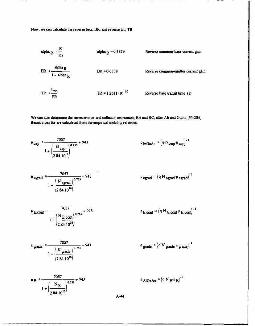
Now, we cam calculate the reverse beta, BR, and reverse tau, TR:
alpha R -IS alpha R = 0.3879 Reverse common-base current gainIcs
BR alpha R BR = 0.6338 Reverse common-anitter current gain
I - alpha R
tnoTR - TR = 1.2611"10-"° Reverse base transit time (s)
BR
We can also determine the senes emitter and collector resistances, RE and RC, after Ali and Gupta [53:2041.Resistivities for are calculated from the empirical mobility relations.
Scap ( 05 ) 0.753 +943 PInGaAs (q-Ncp.ILcap)
1+ N rcap
\2.84.1016
Acrd7057 0.5 93Pcrd (q g!"Lcrd
l+l
E.ont5 0.753 943 PEont = (q.N E.cont. IE.ont)-l NE'cont /'ý
2ý.84.10)e
L grade 7057 0.75 943 P grade (q-N grade- grade)
1 + I Ngrade\2.84.1016/
IE 7 0 943 PAI~aAs = q'N E)7 0.753
A-44

IL C ( 0.753 +943 PC C- ILNC)
IsubC 0.753 +943 PsubC :q N sbCLsubCI (NsubC/°s
Ap- + 60 0.417 +40 PB := (q.N B' p)1
P InGaAs = 3.1423.1074 Estimated resistivity of the InGaAs cap layer (ohm.cm)
p =grad 6.0764- 10- Resistivity of the In graded region (ohm.cm)
P E.cont = 0.0012 Resistivity of the continuous GaAs region (ohm.cm)
P grade 0.0075 Resistivity of the Al graded region (ohm.cm)
P A1GaAs = 0.0075 Estimated resititvity of the AIGaAs emitter region (ohm.cm)
PB =0.0017 Resistivity of the p-type GaAs base (ohm.cm)
p C = 0.0214 Resistivity of the n-type GaAs collector (ohm.cm)
P subC = 0.00 18 Resistivity of the n+ GaAs subcollector (ohm.cm)
PEI := P InGaAs'" cap + (P cgrad) I cgrad + PE.cont'1 E.cont
PE2 =-(P grade)"1 grade +P AIGaAs (I wide- X lo)
A-45

PE :=PEI+ PE2 Composite emitter semiconductor resistance (ohm'm^2)
RE :=± RE 0.24 Compont of emitter resistance due to the semiconductor (ohm)Abe
R PEc RE c 6.5496 Compoent of emitter resistance due to the metallizahon (ohm)Abe
RE =RE s+ REc Total emitter series resistance (ohm) RE = 6.7896
RB for an emitter dot geometry may be calculated with the formula provided by W. Liu, Solid-State Electronics,vol. 36, p. 496, Apr. 93.
:= ' - 0.1.10"4 a I =9"10- 1 Radius ofemitter dot (cm)
2
c- a2 = 1.10 Inner radius of base contact (cm)
21 ee
a3 '- + 1.25.10-4 a3 =2.25-10- Approximat outer radius of base annulus contact (cm)2
PB
R B.sh = PB R B.sh = 235.8873 Base sheet resistance (ohm/sq.)W
Lt -= Lt = 1.4559-10-4 Base contact transfer length (cm)R B~shI0.
The base resistance of a junction transistor is typically the sum of three components. These components aregeometry dependent and are given below [67,69]:
Spreading resistance: R R B.sh R sp = 9.38578-n
Bulkresistance: R bulk - . a Rbu=3"9555
A-46

Lateral contact resistance: R Ic -_ L L , L t L t
2.%Sa 2 ~ (L1 (L ,(u))3 aKIX - i-Kl - .11
R ic =44.7133
R -p +Rbuk ~Total base series resistance (ohm): RB T- bulk+R RB T - 4.8379N do('N fin
However, for S-parameter analysis, the base-collector capacitance is distributed across the base resistance.The base resistance is split into two elements: RB and RBext.
Rsp R bulk + R lcRB:- spRBex
N dotN fin N dotN fin
The capacitance of the base metal-semiconductor contact is in parallel with RBext. However, due to the highbase doping the barrier is very thin and there is essentially no SCR. Tunneling current occurs easily; thusCbcon can be neglected.
The collector resistance is also comprised of spreading, bulk, and lateral contact resistances. When thetransistor is operated in the active region (as is the case for microwave operation), the collector layer is fullydepleted and does not contribute to the series resistance. However, better agreement on the I-Vcharacteristics is obtained when the resistance of the collector layer is considered. When the transistor issaturated, almost the entire collector region is resistive.
R C 4o) R c = 1.8574 Zero-bias collector series resistance (ohm)21 ee.N dot
R subC.sh PsubC R subC.sh = 18.1238 Subcollector sheet resistance (ohm/sq.)subC
! ~ 0.5
L t P = EcS" L t = 3.3219" 107' Collector contact transfer length (cm)R subC-sh
A-47

Since the Collector current enters the subcollector layer through an ae approximately 2x2 microns square (theemitter dot), and then follows two parallel paths, we have:
Spreading resistance: R R - u>s R sp = 0.2517'P 12"N dot
Bulk resistance: R bulk:- =n(2). (R subC.sh) R bulk - 1.046 9I ee' 2"N d
R subC~s cI R1 =.24Lateral contact resistance: R Ic Lt-coth R Ic = 1.2543
2.1 cc Lc t
The total ac collector series resistance may be assumed different than the dc resistance as given by thefollowing expressions:
RC RSP+Rbulc+Rlc RC ac = 1.27 6 5R~aN Nfin
R sp÷ Rbulk÷ Rlc*RC
RC do: N fin RC dc = 2.2051
The two remaining do model parameters are ISE and ISC, the recombination diodes saturation currents. Theseparameters can be estimated by calculating a composite recombination saturation current that is the sum of allthe individual recombination component saturation currents. ISE is the constant for the Vbe exponent andISC is the constant for the Vbc exponent. The analytical expressions for the recombination currentcomponents are found in Rymn and Abdel-Motaleb [45], Liou [52], and Huang and Abdel-Motaleb [66].
The bulk base recombination saturation current expression comes from reference [45], with the exception thatthe drift-diffusion model is used to determine the base-emitter carrier concentrations.
ISE BR: cosh -_I\51fl1-.j_ ISE BR =2.36 07 -1O73
ISE BR no'N B WnB L -nB
A-48

q.Abe*L~nB-i !B WB SBR .60LSCBR t 'NB L- LOB
The SCR recombination saturation currents from reference [66]:
q'Abe [n. /l • niE(+ ni X +niB.X2o ISEscR -3.7089"
ISC SCR =(n- - X 3( nic'X 3) ISC SCR =4.0848"107ISCSCR 2- 2t SRH
The surface recombination saturation current from reference [45]:
ISESR =q.P.SoL sniB ISE SR 2.738"-1
The smi of these individual components are the composite saturation currmts ISE and ISC:
ISE ISE BR + ISE SCR * ISE SR ISE = 3.1089. 10-!$
ISC =ISC BR + ISC SCR ISC = 4.0848- 10-C
The final dc model parameter is the forward knee current which models the degradation of beta at highcurrents.
IKF = q. A be.N c -vt IKF = 0.0489
Since for this device the ;'€:.,tor metal surrounds the base finger, the parasitic base-collectorcapacitance, Cbcp, may b-, cadc'loated as follows:
S (lcl+lbc+leb).lbc] 0.5 = [(lcl+Ibc+clbb).lbc] k S=(I-_ s2)0.
s [ ( eb+ bc).( cl÷bc) ]= [ ( bb÷bc).(Il + lt)
A-49

Kf = [ (5 2 .4 6 -10 7 4+ 1 h e + cc + I b b + 2 6 -10 4).l C r '= I K 5k f ( )[I CC I bb+ 2610'4I)(52.46107 ] + I k)f Kf)
14 110)I-4 kmn -4 m)
(I[ cc+4 +381 .I•2-1.03- . 10. 05
K : I +(, 9-10' 4+ 8 10o4) 39.,o4 1 -17)8 o ], I, -K oe
, 4 1,0 -o4 +,3, 9 .1, o4) ] k t - K
The following constants and function K(k) are the solution to the required integral provided by the NavalResearch Laboratory Report 8561, p. 15, 1982:
A 0 13862944 A 2 :0.0725296 A, =0.l119723
B 0 :=0.5 B l :=0.1213478 B 2 =0.0288729
K(K):m[Ao+AI.(I-K2)+A 2 .(_K2)2]+ lf].[BO+Bl.(l-K2)+B2 .(1-[2)2]
/ K(kl) K(k2) K(kf) l0 b N2t-(p
Cbcpl =2-Nfi.Ndot-lee. (E p +- B) -~ K~ 1) + K )++(21c b\K(KI) K(Ks) K(Kf) ote 1 bc
Cbcp2 :=,pl.-÷ B), [ K(km) 1 10"4 + K(ke)( 1"5' -4)+ K(kt)" 1.5.10 '4-K0(KM) K(Ke) K(Ct)
A-SO

C bap :=C bepl + Cb•p2
coe OT P(AI CC_0.1 )* WE =1cap+Ilcgrad+ IE.cm I *1 pa&dewide
g p.[AbC- Abe+ (Nhinlbb2)] +2.u.cp.(top-.WE) NoN flnhC bep-= deb- 0.1-10" In 0.5.1 ee
-l0.5.1 CCe- 0. 1.-10-'4
There: is also an mindctance associtated with each terminal of the transist~r. The equation for est ilat ng thisind e is given by Ladbrooke [59:991. Only the inte ects NOT beneath the emitter bridge (and NOTpart of the thick pad metal) are considered here since the Mndtance under the bridge is negigible mcomnpm.
7 .10Lq CP o't sub- .55 Lbp =o"tsu(b' 4 )5
23.856.28
N"dot . .. 0 4 .1e e 4L, 1l-Nfi (db- - -+ Lo.o (I _o.0.(- loilbb +2-Ieb/ N i
Lcpl :=IO.°(I e c- 1 0"I I 78 I0+ I( N f n ÷ ) - lC L c p l L b l
The resistance m geries with each iductance can be calculated from Ladbrooke (59:146]:
R - PAu.lcc78.10 Rqffi=0.Oll3.tcp (N fm÷ l)-Icl
N" '~.Au i ice I CC.9iR bp-' R bp - 0.0915
Nfh 3 .Itp Ibb 2 .1 e/
A-51

The following are six parasitic equivalent circuit clmenxts that are external to the SPICE BiT model:
C p=2.5754,10-4 The parasitic interelectrode base-collector capecitcame (F)
C bep = 9.877-16-" The parasitic mterelectrode base-anitter capacitance (F)
C cep =3.3689-0-I14 The parasitic intemelectrode collector-emitter capacitsnce (F)
L p = 2.992"16IOl The parasitic collector inducta• e )
L bp = 1.0629.1010 The parasitic base inductance (H)
L ep = 1.5366-10-12 The parasitic emitter inductance (H)
All of the calculated SPICE model parameters are summarized below for the 2 micron emitter, 6 dot two fingergeometry.
BF = 83.9258 Forward common-emitter current gain
BR = 0.6338 Reverse common-emitter current gain
TF = 9.5243-10-13 Forward base transit time (s)
TR = 1.2611-1-ll 1 Reverse base transit time (s)
IS = 1.11,110.-25 Transport saturation current (A)
ISE = 3.1089" 10- Base-emitter leakage saturation current (A)
ISC = 4.0848-10- Base-collector leakage saturation current (A)
RE = 6.7896 Emitter series resistance (ohm)
RB = 0.7821 Intrinsic base series resistance (ohm)
RB T = 4.8379 Total base series resistance (ohm)
RC ac = 1.2765 Microwave collector series resistance (ohm)
A-52

RC o --2.2051 DC ,oohc urns rmigme (ohm)
CE - 4.8855-10 Bmniirtle zo•,,, depletion cpecatuae (F)
CJC - 1.5758- 16-13 Be-codkctor zero-bias depletion capait••e (F)
VJE - 1.7018 Ban-emitter built-in potential (V)
VJC - 1.4107 Base-collector built-in potential (V)
XCJC -0.159 Fraction of bae-collector depletion capacita= internal to baoe
IKF - 0.0489 Corne for high current BF roll-off (A)
The following is an equivalnt cncuit element that is external to the SPICE BJT model:
RB ex - 4.0557 The base contact resistma e (ohm)
A-53

Appendix B: NSPICZ Files
B-1

DC IIPICB Wilos
*,
"* SPICE HBT I-V Characteristics"* Author: James A. Fellows"* Date: 22 Oct 93"* Filename: ldn dclO.sp"* Technology: AlGaAs/GaAs Heterojunction Bipolar"* Description: This file provides dc data for an NPN HBT (4490A,* single dot 3 micron emitter).
* Voltage Source (+) node (-) node Value
Vce C 0 $ swept
* Current Source (+) node (-) node Value
Ib 0 B $ swept
* Circuit Elements (+) node (-) node Value
Rsrc B 0 le+20
* BT Collector Base Emitter Model
Q1 C B GND T3uldlf
.option brief post
* DC Voltage/Current Sweeps: Modify step to match measured data
* Volt(l) Start End Step Crnt(l) Start End Step
.dc Vce 0 4 0.05 Ib 20u 200u 20u
* Data to be collected:
* Vce Vbe Ib Ic
.print dc v(C), v(B), i(Ib), i(Vce)
.model T3uldlf npn"+ BF - 28.9 BR - 0.005 NF - 1.116"+ NR - 1.00000"+ RB - 43.2846 RE - 33.6707 RC - 68.7"+ IS - 1.0363e-26
B-2

"+ CJE - 9.8515e-15 MJE - .50 VJE - 1.7018"+ CJC - 1.119e-14 MJC - .50 VJC - 1.3691"+ TF - 9.5681e-13 TR - 5.287e-10 XCJC - 0.2053
.end
* SPICE HBT I-V Characteristics* Author: James A. Fellows* Date: 22 Oct 93* Filename: 5dndclO.sp* Technology: AIGaAs/GaAs Heterojunction Bipolar* Description: This file provides dc data for an NPN HBT (4491,* 5 dot, single finger 3 micron emitter).
* Voltage Source (+) node (-) node Value
Vce C 0 $ swept
* Current Source (+) node (-) node Value
Ib 0 B $ swept
*,=
* Circuit Elements (+) node (-) node Value
Rsrc B 0 le+20
* BT Collector Base Emitter Model
Ql C B GND T3u5dlf
.option brief post
* DC Voltage/Current Sweeps: Modify step to match measured data
* Volt(l) Start End Step Crnt(l) Start End Step
.dc Vce 0 4 0.05 Ib 50u 200u 50u
* Data to be collected:*=
* Vce Vbe Ib Ic
.print dc v(C), v(B), i(Ib), i(Vce)
B-3

.�- . ' •i ,�' -
.model T3u5dlf npn"+ BF - 33.3 BR - 0.0231 NF - 1.1557"+ NR - 1.00000"+ RB - 8.6569 RE - 6.7341 RC - 16.79"+ IS - 5.2047e-26"+ CJE - 4.9257e-14 MJE - .50 VJE - 1.7018"+ CJC - 3.5706e-14 MJC - .50 VJC - 1.3454"+ TF - 9.5811e-13 TR - 1.4046e-09 XCJC - 0.2053
.end
"* SPICE HBT I-V Characteristics"* Author: James A. Fellows"* Date: 22 Oct 93"* Filename: 6dn dclO.sp"* Technology: AlGaAs/GaAs Heterojunction Bipolar"* Description: This file provides dc data for an NPN HBT (4457B,* 6 dot, 2 finger 2 micron emitter).
* Voltage Source (+) node (-) node Value
Vce C 0 $ swept
* Current Source (+) node (-) node Value
Ib 0 B $ swept
.
* Circuit Elements (+) node (-) node Value
Rsrc B 0 le+20
.
* BJT Collector Base Emitter Model
Ql C B GND T2u6d2f
.option brief post
* DC Voltage/Current Sweeps: Modify step to match measured data
* Volt(l) Start End Step Crnt(l) Start End Step
.dc Vce 0 3 0.05 Ib lOOu llOOu lOOu
B-4

* Data to be collected:*.
* Vce Vbe Ib Ic
.print dc v(C), v(B), i(Ib), i(Vce)
.model T2u6d2f npn"+ BF 83.926 BR - 0.6338 NF 1.1049"+ NR 1.00000 NE - 1.7000 NC - 1.7595"+ RB 4.8379 RE - 6.7896 RC - 2.2"+ IS 1.1111e-25 ISE - 2.432e-19 ISC - 4.393e-16"+ CJE 4.8855e-14 MJE - .50 VJE - 1.7018"+ CJC 1.5758e-13 MJC - .50 VJC - 1.4107"+ TF 9.5243e-13 TR - 1.2611e-10 XCJC - 0.159
.end
Microwave HSPICE Files
*,
* SPICE HBT S-Parameter Analysis* Author: James A. Fellows* Date: 22 Oct 93* Filename: 1F_21_N.sp* Technology: AlGaAs/GaAs Heterojunction Bipolar* Description: This file provides S-parameter data for an NPN HBT* (4490A: single dot, 3 micron emitter).*.
.net i(Vce) Ib ROUT-50 RIN-50
* Voltage Source (+) node (-) node Value
Vce CC 0 2
* Current Source (+) node (-) node AC value DC value
Ib 0 BB AC-I DC-IOOu
* Circuit Elements (+) node (-) node Value
Rsrc BB 0 le+20RBext B Bcon 33.8989Cbep Bcon E 0.739fCbcp C Bcon 15.OfCcep C E 0.lfLep E 0 1.69•5pLbp Bcon BB 1.6965p
B-5

Lcp C CC 3.309p
* BJT Collector Base Emitter Model
Qi C B E T3uldlf
.option brief post
* AC Frequency Sweeps: Modify step to match measured data
* Scale Points Start Stop
.ac LIN 50 iC 50G
.
* Data to be collected: S-Parameters (M)agnitude and (P)hase
.print ac Sll(M) Sll(P) S21(M) S21(P) S12(M) S12(P) $22(M) S22(P)
.model T3uldlf npn"+ BF - 28.9 BR - O.00W NF - 1.116"+ NR - 1.00000"+ RB - 9.3857 RE - 33.6707 RC - 68.7"+ IS - 1.0363e-26"+ CJE - 9.8515e-15 MJE - .50 VJE - 1.7018"+ CJC - 1.119e-14 MJC - .50 VJC - 1.3691"+ TF - 9.5681e-13 TR - 5.287e-10 XCJC - 0.2053
.end
"* SPICE HBT S-Parameter Analysis"* Author: James A. Fellows"* Date: 22 Oct 93"* Filename: 5F_23_N.sp"* Technology: AlGaAs/GaAs Heterojunction Bipolar"* Description: This file provides S-parameter data for an NPN HBT* (4491A: 5 dot, single finger, 3 micron emitter).
.net i(Vce) Ib ROUT-50 RIN-50
* Voltage Source (+) node (-) node Value
Vce CC 0 1
B-6

* Current Source (+) node (-) node AC value DC value
Ib 0 BB AC-i DC-500u
* Circuit Elements (+) node (-) node Value
Rsrc BB 0 le+20RBext B Bcon 6.7798Cbep Bcon E 3.6943fCbcp C Bcon 31.566fCcep C E 13.65fLep E 0 1.4224pLbp Bcon BB 8.4823pLcp C CC 1.709p
* BJT Collector Base Emitter Model
Q1 C B E T3u5dlf
.option brief post
* AC Frequency Sweeps: Modify step to match measured data
* Scale Points Start Stop
.ac LIN 50 SO 50G
* Data to be collected: S-Parameters (M)agnitude and (P)hase
.print ac SIl(M) SII(P) S21(M) S21(P) S12(M) S12(P) $22(M) $22(P)
.model T3u5dlf npn"+ BF - 33.3 BR - 0.0231 NF - 1.1557"+ NR - 1.00000"+ RB - 1.8771 RE - 6.7341 RC - 16.79"+ IS - 5.2047e-26"+ CJE - 4.9257e-14 MJE - .50 VJE - 1.7018"+ CJC - 3.5706e-14 MJC - .50 VJC - 1.3454"+ TF - 9.5811e-13 TR - 1.4046e-09 XCJC - 0.2053
.end
B-7

"* SPICE HBT S-Parameter Analysis"* Author: James A. Fellows"* Date: 22 Aug 93"* Filename: 6F_81_N.sp"* Technology: AlGaAs/GaAs Heterojunction Bipolar"* Description: This file provides S-parameter data for an NPN HBT* (4457B: 6 dot, 2 finger, 2 micron emitter).
.net i(Vce) Ib ROUT-50 RIN-50
* Voltage Source (+) node (-) node Value
Vce CC 0 1
.
* Current Source (+) node (-) node AC value DC value
Ib 0 BB AC-l DC-800u
* Circuit Elements (+) node (-) node Value
Rsrc BB 0 le+20RBext B Bcon 4.0557Cbep Bcon E 7.3255fCbcp C Bcon 106.136fCcep C E 18.488fLep E 0 0.4841pLbp Bcon BB 2.3562pLcp C CC 0.6093p
* BJT Collector Base Emitter Model
Ql C B E T2u6d2f
.option brief post
* AC Frequency Sweeps: Modify step to match measured data
* Scale Points Start Stop
.ac LIN 50 1G 50G
* Data to be collected: S-Parameters (M)agnitude and (P)hase
.print ac SII(M) SlI(P) S21(M) S21(P) S12(M) S12(P) $22(M) S22(P)
B-8

.model T2u6d2f npn"+ BF - 83.926 BR 0.6338 NF 1.1049"+ NR - 1.00000 NE - 1.7000 NC - 1.7595"+ RB - 0.7821 RE - 6.7896 RC - 2.2"+ IS - 1.1111e-25 ISE - 2.432e-19 ISC - 4.393e-16"+ CJE - 4.8855e-14 MJE - .50 VJE - 1.7018"+ CJC - 1.5758e-13 MJC - .50 VJC - 1.4107"+ TF - 9.5243e-13 TR - 1.2611e-10 XCJC - 0.159
.end
HBPICB Optimization Files
"* Optimization of SPICE HBT I-V Characteristics"* Author: James A. Fellows"* Date: 21 )ct 93"* Filename: 6d-fit.sp"* Technology: AlGaAs/GaAs Heterojunction Bipolar"* Description: This file optimizes six SPICE BJT model parameters to
fit the measured data for an NPN HBT (4457B, 2 micronemitter, 6 dot, 2 finger).
* Voltage Source (+) node (-) node Value
Vce C 0 Vce
* Current Source (+) node (-) node Value
Ib 0 B Ib
* Circuit Elements (+) node (-) node Value.
Rsrc B 0 le+20
* BJT Collector Base Emitter Model
Q1 C B GND T2u6d2f
.option post ingold-1
* Physics-based HBT model parameters:
.model T2u6d2f npn"+ BF - 83.926 BR - 0.6338 NF - NF"+ NR - 1.00000 NE - NE NC - NC"+ RB - 4.8379 RE - 6.7896 RC - 2.2
B-9

"+ IS - 1.1111e-25 ISE - ISE ISC - ISC"+ CJE - 4.8855e-14 MJE - .50 VWE - 1.7018"+ CJC - 1.5758e-13 M.JC - .50 VJC - 1.4107"+ TF - 9.5243e-13 TR - 1.2611e-10 XCJC - 0.159
* These are the empirical curve-fit model parameters:
.param NF - optl(1.1, 1.0, 1.2)+ NE - optl(l.9, 1.7, 2.1)+ NC - optl(1.95, 1.75, 2.1)+ ISE - optl(3.lle-18, le-20, le-16)+ ISC - optl(5e-14, le-16, le-13)
.
* dc optimization analysis statement:,
.dc data-measured optimize-optl results-Ib,Ic,Vce,Vbe"+ model-converge Vce LIN 31 0.0 3.0 sweep"+ Ib LIN 11 100u ll00u
.model converge opt itropt-l00 grad-le-05
.meas dc Ib errl par(Ib) i(ib)
.meas dc Ic errl par(Ic) i(vce)
.meas dc Vce errl par(Vce) v(c)
.meas dc Vbe errl par(Vbe) v(b)
.dc data-measured
* Measured data to fit model parameters:
.data measured
Vbe Vce Ic Ib
1.07599998 0.00000000 0.00009878 0.000100001.17499995 0.10000000 0.00009342 0.00010000
1.76400006 1.10000000 -0.04613100 0.00110000
.enddata
.end
2u6d2f dc optimization results:
residual sum of squares - 5.95116norm of the gradient - 23.6635marquardt scaling parameter - 0.492699no. of function evaluations - 234
B-10

no. of iterations - 66
optimization completed
parameters < relin- 1.OOOOE-03 on last iterations
**** optimized parameters optl%norm-sen %change
.param nf - 1.1049 $ 49.5075 -7.462e-04
.param ne - 1.7000 $ 48.3361 3.837e-04
.param nc - 1.7595 $ 0.7342 -2.402e-03
.param ise - 2.432e-19 $ 1.3952 -2.231e-02
.param isc - 4.393e-16 $ 2.698e-02 -4.936e-02
"* Optimization of HBT S-Parameters by Fitting Parasitics"* Author: James A. Fellows"* Date: 21 Oct 93"* Filename: 6dotac.sp"* Technology: AlGaAs/GaAs Heterojunction Bipolar"* Description: This file provides S-parameter data for an NPN HBT* (4457B: 6 dot, 2 finger, 2 micron emitter).
.net i(Vce) Ib ROUT-50 RIN-50
* Voltage Source (+) node (-) node Value
Vce CC 0 1
,
* Current Source (+) node (-) node AC Value DC Value*
Ib 0 BB AC-l DC-800u
* Circuit Elements (+) node (-) node Value
Rsrc BB 0 le+20Rbcon B Bcon 4.0557Cbep Bcon E CbepCbcp C Bcon CbcpCcep C E CcepLep E 0 LapLbp Bcon BB LbpLep C CC Lcp
B-Il

* UT Collector Base Emitter Model
Qi C B E T2u6d2f
.option post ingold-l
.model T2u6d2f npn"+ BF - 83.926 BR - 0.6338 NF - 1.1049"+ NR - 1.00000 NE - 1.7000 NC - 1.7595"* RB - 4.8379 RE - 6.7896 RC - 2.2"+ IS M 1.1111e-25 ISE - 2.432e-19 ISC - 4.393e-16"+ WE - 4.8855e-14 W.E - .50 VWE - 1.7018"+ CJC - 1.5758e-13 MJC - .50 VJC - 1.4107"+ TF - 9.5243e-13 TI - l.2611e-lO XCJC - 0.159
*These are the empirical curve-fit model parameters:
.param Cbep -opti(6f, if, 30f)"+ Cbcp - optl(7.6f, if, 114f)"+ Ccep - optl(18.5f, 3.7f, 92.5f)"+ Lep - optl(15p, 0.3p, 30p)"+ Lbp - opti(40p, 8p, 85p)"+ Lcp - optl(20p, 5p, 50p)
*ac optimization analysis statement:
ac data-measured or#pimize-opti results-SliR, SI, S12R, 5121,+ S21R,S211,S22R,S22I model-converge LIN 50 1 50
.model converge opt itropt-40 grad-le-04
.meas ac SilR erri par(S11R) ýS11(R)incas ac S1Il erri par(S11I) S11(I).meas ac; S12R erri par(S12R) S12(R).meas ac Si21 erri par(Sl21) S12(I).ncas ac S21R erri par(S21R) S21(R).meas ac S21I erri par(S211) S21(I).meas ac S22R erri par(S22R) S22(R).meas ac S221 errl par(S221) S22(I)
.ac data-measured
*Measured data to fit model parasitics:
.data measured
B-12
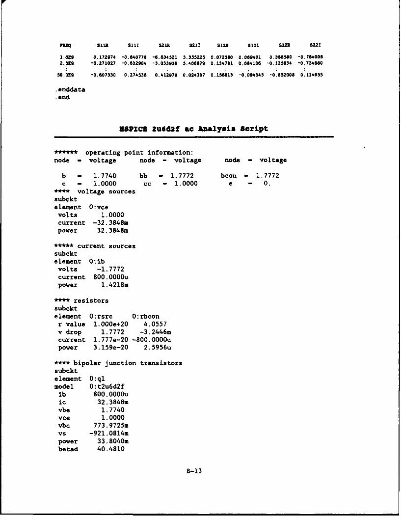
hM SURl SSi 521R 5211 S12 5121 SiE S221
1.039 0.172974 -0.640778 -6.834521 5.355225 0.072590 0.089401 0.388580 -0.7640082.039 -0.271027 -0.632904 -3.033936 5.400879 0.134781 0.084106 -0.135834 -0.73460
50.o09 -0.607330 0.274536 0.412979 0.024307 0.15813 -0.094345 -0.552006 0.114655
.enddata
.end
ISPICE 2u6d2f ac Analysis Script
• ***** operating point information:node - voltage node - voltage node - voltage
b - 1.7740 bb - 1.7772 bcon - 1.7772c - 1.0000 cc - 1.0000 e - 0.
**** voltage sourcessubcktelement O:vcevolts 1.0000current -32.3848mpower 32.3848m
**** current sourcessubcktelement 0:ibvolts -1.7772current 800.0000upower 1.4218m
**** resistorssubcktelement O:rsrc O:rbcon
r value 1.000e+20 4.0557v drop 1.7772 -3.2446mcurrent 1.777e-20 -800.O000upower 3.159e-20 2.5956u
**** bipolar junction transistorssubcktelement O:qlmodel 0:t2u6d2f
ib 800.O000uic 32.3848mvbe 1.7740vce 1.0000vbc 773.9725mvs -921.0814mpower 33.8040mbetad 40.4810
B-13
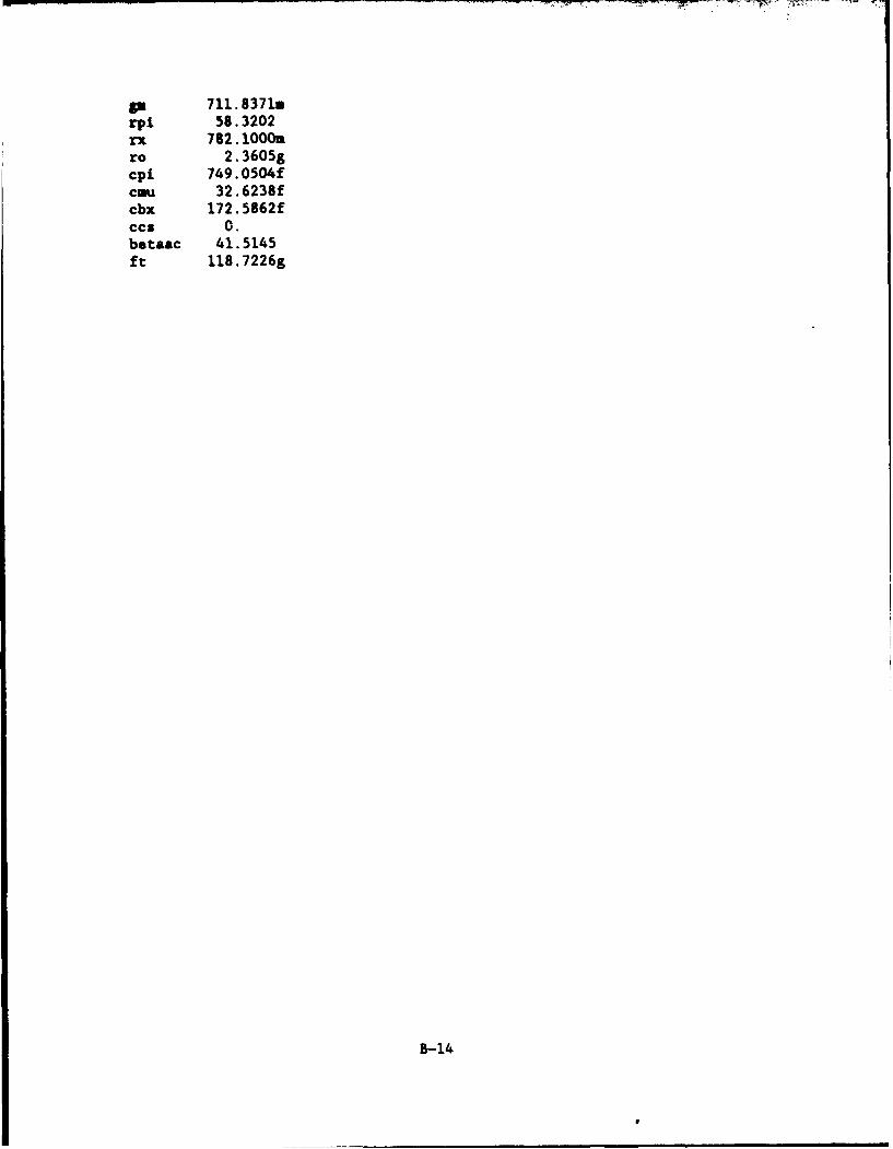
5um 711.8371mrpi 58.3202rx 782.1000mro 2.3605gcpi 749.0504fcou 32.6238fcbx 172.5862fccs 0.betaac 41.5145ft 118.7226g
B-14
FiI
[1] P. M. Asbeck, M. F. Chang, J. A. Higgins, N. H. Sheng, G. J.Sullivan, and K.-C. Wang, "GaA1As/GaAs Heterojunction BipolarTransistors: Issues and Prospects for Application," IEEE Trans.Electron Dev., vol. 36, pp. 2032-2041, Oct. 1989.
[2] P. M. Asbeck, M. F. Chang, K.-C. Wang, D. L. Miller, G. J. Sullivan,N. H. Sheng, E. Sovero, and J. A. Higgins, "Heterojunction BipolarTransistors for Microwave and Millimeter-wave Integrated Circuits,"IEEE Trans. Electron Dev., vol. 34, pp. 2571-2579, Dec. 1987.
[3] M. E. Kim, A. K. Oki, G. M. Gorman, D. K. Umemoto, and J. B. Camou,"GaAs Heterojunction Bipolar Transistor Device and IC Technology forHigh-Performance Analog and Microwave Applications," IEEE Trans.Microwave Theory Tech., vol. 37, pp. 1286-1302, Sep. 1989.
[4] M. Konagi and K. Takahashi, "(GaAl)As-GaAs HeterojunctionTransistors with High Injection Efficiency," J. Appl. Phys., vol.46, pp. 2120-2123, May 1975.
[5] H. Ito, T. Ishibashi, and T. Sugeta, "Fabrication andCharacterization of AlGaAs/GaAs Heterojunction Bipolar Transistors,IEEE Trans. Electron Dev., vol. 34, pp. 224-229, Feb. 1987.
[6] F. Ali, M. Salib, and A. Gupta, "A 1-Watt X-Ku Band HBT MMICAmplifier with 50% Peak Power-Added Effieciency," IEEE Microwave andGuided Wave Letters, vol. 3, pp. 271-272, Aug. 1993.
[7] B. Bayraktaroglu, J. Barrette, L. Kehias, C. Huang, R. Fitch, R.Neidhard, and R. Scherer, "Very High-Power-Density CW Operation ofGaAs/AIGaAs Microwave Heterojunction Bipolar Transistors," IEEEElectron Device Letters, vol. 14, pp. 493-495, Oct. 1993.
[8] M. Hafizi, R. A. Metzger, and W. E. Stanchina, "Dependence of DCCurrent Gain and f.. of AlInAs/GaInAs HBTs on Base SheetResistance," IEEE Electron Device Letters, vol. 14, pp. 323-325,Jul. 1993.
[9] F. Ren, C. R. Abernathy, S. J. Pearton, J. R. Lothian, P. W. Wisk,T. R. Fullowan, Y.-K. Chen, L. W. Yang, S. T. Fu, and R. S.Brozovich, "Self-Aligned InGaP/GaAs Heterojunction BipolarTransistors for Microwave Power Application," IEEE Electron DeviceLetters, vol. 14, pp. 332-334, Jul. 1993.
[10] W. Matsuoka, K. Kurishima, and T. Makimoto, "High-frequencyInP/InGaAs Double Heterojunction Bipolar Transistors on SiSubstrate," IEEE Electron Device Letters, vol. 14, pp. 357-359, Jul.1993.
Bib-I

[11] K. Ikossi-Anastasiou, "GaAsSb for Heterojunction BipolarTransistors," IEEE Trans. Electron Dev., vol. 40, pp. 878-884, May1993.
[12] J. Chen, G. B. Gao, and H. H. Morkoq, "Comparative Analysis of theHigh-Frequency Performance of Si/SilGe. Heterojunction Bipolar andSi Bipolar Transistors," Solid-State Electronics, vol. 35, pp. 1037-1044, Aug. 1992.
[13] W. Till and J. Luxon, Integrated Circuits: Materials, Devices andFabrication, Prentice-Hall, NJ, 1982.
[14] S. M. Sze, Physics of Semiconductor Devices, John Wiley and Sons,NY, 1981.
[15] S. M. Sze, ed., High-Speed Semiconductor Devices, John Wiley andSons, NY, 1990.
[16] T. Ikoma, ed., Very High Speed Integrated Circuits:Heterostructure, Semiconductors and Semimetals, Vol 30, AcademicPress, CA, 1990.
[17] H. Kroemer, "Heterostructure Bipolar Transistors and IntegratedCircuits," Proceedings of the IEEE, vol. 70, pp. 13-25, Jan. 1982.
[18] H. Kroemer, "Theory of a Wide-Gap Emitter for Transistors,"Proceedings of the IRE, vol. 45, pp. 1353-1357, 1957.
[19] W. Shockley, U. S. Patent no. 2,569,347 assigned to W. Shockley, Jun26, 1948.
[20] W. Dumke, J. Woodall, and V. Rideout, "GaAs-GaAlAs HeterojunctionTransistor for High Frequency Operation," Solid-State Electronics,vol. 15, pp. 1339-1334, Dec. 1972.
[21] P. Antognetti and G. Massobrio, eds., Semiconductor Device Modelingwith SPICE, McGraw-Hill, NY, 1988.
[221 S.J. Wang, J.Y. Lee and C.Y. Chang, "An Efficient and ReliableApproach for Semiconductor Device Parameter Extraction," IEEETransactions on Computer-Aided Design, vol. 5, pp. 170-178, Jan.1986.
[23] B. Ryum and I. Abdel-Motaleb, "A Gummel-Poon Model for Abrupt andGraded Heterojunction Bipolar Transistors (HBTs)," Solid-StateElectronics, vol. 33, pp. 869-880, July 1990.
[24] C. Parikh and F. Lindholm, "A New Charge-Control Model for Single-and Double-Heteroj unction Bipolar Transistors," IEEE Trans. ElectronDev., vol. 39, pp. 1303-1311, June 1992.
Bib-2
[25] P. Grossman and J. Choma, "Large Signal Modeling of HBT's IncludingSelf Heating and Transit Time Effects," IEEE Trans. Microwave Theoryand Techniques, vol. 40, pp. 449-463, March 1992.
[26] M. Hafizi, C. Crowell, and M. Grupen, "The DC Characteristics ofGaAs/AlGaAs Heterojunction Bipolar Transistors with Application toDevice Modeling," IEEE Trans. Electron Devices, vol. 37, pp. 2121-2129, Oct. 1990.
[27] J. J. Liou and J. S. Yuan, "Physics-based Large-siganlHeterojunction Bipolar Transistor Model for Circuit Simulation," IEEProceedings-G, vol. 138, pp. 97-103, Feb. 1991.
[28] D. Pehlke and D. Pavlidis, "Evaluation of the Factors DeterminingHBT High-frequency Performance by Direct Analysis of S-ParameterData," IEEE Trans. Microwave Theory and Techniques, vol. 40, pp.2367-2373, Dec. 1992.
[29] S. Maas and D. Tait, "Parameter Extraction Method for HeterojunctionBipolar Transistors," IEEE Microwave and Guided Wave Letters, vol.2, pp. 502-504, Dec. 1992.
[30] R. Trew, U. Mishra, W. Pribble, and J. Jensen, "A ParameterExtraction Technique for Heterojunction Bipolar Transistors," 1989IEEE MTT-S Digest, pp. 897-900.
[31] D. Costa, W. Liu, and J. Harris, Jr., "Direct Extraction of theAlGaAs/GaAs Heterojunction Bipolar Transistor Small-SignalEquivalent Circuit," IEEE Trans. Electron Devices, vol. 38, pp.2018-2024, Sep. 1991.
[32] J. J. Liou, L. L. Liou, C. I. Huang, and B. Bayraktaroglu, "APhysics-Based, Analytical Heterojunction Bipolar Transistor ModelIncluding Thermal and High-Current Effects," IEEE Trans. ElectronDev., vol. 40, pp. 1570-1577, Sep. 1993.
[33] H. Wang, C. Algani, A. Konczykowska, and W. Zuberek, "TemperatureDependence of DC Currents in HBT," 1992 IEEE MTT-S Digest, pp. 731-734.
[34] M. Hafizi, W. E. Stanchina, R. A. Metzger, P. A. Macdonald, and F.Williams, Jr., "Temperature Dependence of DC and RF Characteristicsof AlInAs/GaInAs HBT's," IEEE Trans. Electron Dev., vol. 40, pp.1583-1587, Sep. 1993.
[35] D. S. Whitefield, D. S. Wei, and J. C. Hwang, "Large SignalCharacterization and Modelling of Heterojunction-Bipolar TransistorsAnnual Report," Report No. AD-A253011, June 1, 1991-May 31, 1992.
[36] C. C. McAndrew, "A Complete and Consistent Electrical/Thermal HBTModel," IEEE 1992 Bipolar Circuits and Technology Meeting, paper10.1, pp. 200-203.
Bib-3

[37] A. Marty, T. Camps, J. Tasselli, D. Pulfrey, and J. P. lailbe, "ASelf-Consistent DC-AC Two Dimensional Electrothermal Model forGaAlAs/GaAs Microwave Power HBT's," IEEE Trans. Electron Dev., vol.40, pp. 1202-1210, July 1993.
[38] Mathcad Version 3.1, 1992. MathSoft Inc., 201 Broadway, Cambridge,MA 02139.
[39] HSPICE User's Manual, vol. 2, Elements and Models, HSPICE VersionH92, 1992. Meta-Software, Inc., Customer Service Dept., 1300 WhiteOaks Rd., Campbell, CA 95008.
[40] HSPICE User's Manual, vol. 3, Analysis and Methods, HSPICE VersionH92, 1992. Meta-Software, Inc., Customer Service Dept., 1300 WhiteOaks Rd., Campbell, CA 95008.
[41] Axum Technical Graphics and Data Analysis, Third edition, 1993.Trimetrix, Inc., 444 NE Ravenna Blvd., Suite 210, Technical SupportDept., Seattle, WA 98115.
[42] Designer's Task Reference, vol. 2, Creating Circuits as Schematics,HP 85150B Microwave and RF Design Systems, Release 5.0, edition 2Dec. 1992. Hewlett-Packard Company, Santa Rosa Systems Div., 1400Fountaingrove Pkwy., Santa Rosa, CA 95403.
[43] J. Ebers and J. Moll, "Large-Signal Behavior of JunctionTransistors," Proceedings of the IRE, vol. 42, pp. 1761-1772, 1954.
[44] H. Gummel and H. Poon, "An Integral Charge Control Model of BipolarTransistors," Bell Systems Technical Journal, vol. 49, pp. 827-852,May 1970.
[45] D. Hodges and H. Jackson, Analysis and Design of Digital IntegratedCircuits, McGraw-Hill, NY, 1988.
[46] B. R. Ryum and I. M. Abdel-Motaleb, "Effect of Recombination Currenton Current Gain of HBTs," 1EE Proceedings-G, vol. 138, pp. 115-119,Feb. 1991.
[47] J. Yoshida, M. Kurata, K. Morizuka, and A. Hojo, "Emitter-baseBandgap Grading Effects on GaAlAs/GaAs Heterojunction BipolarTransistor Characteristics," IEEE Trans. Electron Dev., vol. 32, pp.1714-1720, Sep. 1985.
[48] K. Yokoyama, M. Tomizawa, and A. Yoshii, "Accurate Modeling ofAlGaAs/GaAs Heterostructure Bipolar Transistor by Two DimensionalComputer Simulation," IEEE Trans. Electron Dev., vol. 31, pp. 1222-1229, Sep. 1984.
[49] P. Grossman and A. Oki, "A Large Signal DC Model for GaAs/Ga1 _.1AlxAsHeterojunction Bipolar Transistors," IEEE 1989 Bipolar Circuits andTechnology Meeting, paper 9.6, pp. 258-261.
Bib-4

(50] W. Shockley, "The Theory of p-n Junctions in Semiconductors and p-nJunction Transistors," Bell Systems Technical Journal, vol. 28, pp.435-489, July 1949.
(511 S. M. Sze, Semiconductor Devices, Physics and Technology, John Wileyand Sons, NY, 1985.
[52] J. J. Liou, "Calculation of the Base Current Components andDetermination of Their Relative Importance in AlGaAs/GaAs andInAlAs/InGaAs Heterojunction Bipolar Transistors," J. Appl. Phys.,vol. 69, pp. 3328-3334, Mar 1991.
[53] F. Ali and A. Gupta, eds., HEMTs and HBTs: Devices, Fabrication andCircuits, Artech House, MA, 1991.
[54] D. Pozar, Microwave Engineering, MA, Addison-Wesley, 1990.
[55] T. S. Laverghetta, Practical Microwaves, IN, Howard W. Sams & Co.,1984.
[56] C. R. Selvakumar, "A New Minority Carrier Lifetime Model for HeavilyDoped GaAs and InGaAsP to Obtain Analytical Solutions," Solid-StateElectronics, vol. 30, pp. 773-774, July 1991.
[57] M. S. Lundstrom, M. E. Klausmeier-Brown, M. R. Melloch, R. K.Ahrenkiel, and B. M. Keyes, "Device-related Material Properties ofHeavily Doped Gallium Arsenide," Solid-State Electronics, vol. 33,pp. 693-704, June 1990.
[58] D. M. Caughey and R. E. Thomas, "Carrier Mobilities in SiliconEmpirically Related to Doping and Field," Proceedings of the IEEE,vol. 55, pp. 2192-2193, Dec. 1967.
[59] S. Adachi, "GaAs, AlAs, and Al.Gal.As: Material Parameters for Usein Research and Device Applications," J. Appl. Phys., vol. 58, pp.Rl-R29, Aug. 1985.
[60] P. H. Ladbrooke, MMIC Design: GaAs FETs and HEMTs, MA, Artech House,Inc., 1989.
[61] WL/ELR HBT Layout Design
[62] M. Lundstrom, "An Ebers-Moll Model for the Heterostructure BipolarTransistor," Solid-State Electronics, vol. 29, pp. 1173-1179, 1986.
[63] H. F. Cooke, "Microwave Transistors: Theory and Design," Proceedingsof the IEEE, vol. 59, pp. 1163-1181, Aug. 1971.
[64] D. V. Morgan and M. J. Howes, eds., Microwave Solid-State Devicesand Applications, pp. 30-35, Peter Peregrinus Ltd. Stevenage, UK,1980.
Bib-5

[65] W. Liu, D. Costa, and J. S. Harris, Jr., "Derivation of the Emitter-collector Transit Time of Heterojunction Bipolar Transistors,"Solid-State Electrrnics, vol. 35, pp. 541-545, Apr. 1992.
[66] J. J. Liou, "Common-emitter current gain of AlGalAs/GaAs/GaAsheterojunction bipolar transistors operating at small collectorcurrent," IEEE Trans. Electron Dev., vol. 36, pp. 1850-1852, Sep.1989.
[67] C. N. Huang and I. M. Abdel-Motaleb, "Gummel-Poon model for singleand double heterojunction bipolar transistors," IEE Proceedings-G,vol. 138, pp. 165-169, Apr. 1991.
[68] A. B. Phillips, Transistor Engineering and Introduction toIntegrated Semiconductor Circuits, pp. 211-216, McGraw-Hill, NY,1962.
[69] D. Ferry, ed., Gallium Arsenide Technology Volume 2, Howard W. Sams& Co., IN, 1990.
[70] V. Ya. Niskov and G. A. Kubetskii, "Resistance of Ohmic ContactsBetween Metals and Semiconductor Films," Soviet Physics -Semiconductors, vol. 4, pp. 1553-1554, Mar. 1971.
[71] "GaAs/A1GaAs HBT Analog-to-Digital Converter," Rockwell, WRDC-TR-89-5041, Oct. 1989.
[72] H.-F. Chau and E. A. Beam, III, "High-Speed InP/InGaAsHeterojunction Bipolar Transistors," IEEE Electron Device Letters,vol. 14, pp. 388-390, Aug. 1993.
[73] B. Meskoob, S. Prasad, M. Vai, C. G. Fonstad, J. C. Vlcek, H. Sato,and C. Bulutay, "A Small-Signal Equivalent Circuit for theCollector-Up InGaAs/InAlAs/InP Heterojunction Bipolar Transistor,"IEEE Trans. Electron Dev., vol. 40, pp. 2629-2632, Nov. 1992.
[74] R. F. Harrington, Introduction to Electromagnetic Engineering,
McGraw-Hill, NY, 1958.
[75] Smythe, Static and Dynamic Electricity, 1968.
[76] B. Meskoob, S. Prasad, M. Vai, J. C. Vlcek, H. Sato, and C. C.Fonstad, "Bias-Dependence of the Intrinsic Element Values ofInGaAs/InAlAs/InP Inverted Heterojunction Bipolar Transistor," IEEETrans. Microwave Theory Tech., vol. 40, pp. 1012-1014, May 1992.
Bib-6

[771 C. T. Matsuno, A. K. Sharma, and A. K. Oki, "A Large-Signal HSPICEModel for the Heterojunction Bipolar Transistor," IEEE Trans.Microwave Theory Tech., vol. 37, pp. 1472-1474, Sep. 1989.
[78] D. A. Teeter, J. R. East, R. K. Mains, and G. I. Haddad, "Large-Signal Numerical and Analytical HBT Models," IEEE Trans. ElectronDev., vol. 40, pp. 837-845, May 1993.
Bib-7
Vita
James A. Fellows was born on August 13, 1965, in Concord, New
Hampshire. In May 1987, he graduated with distinction from Clarkson
University with a Bachelor of Science degree in Electrical Engineering and
was commissioned as a Second Lieutenant in the United States Air Force.
His first assignment began in January 1988 at Los Angeles AFB, California,
where he was a Communications Project Engineering Manager for the Air
Force Satellite Control Network (AFSCN). In April 1992, he entered the
School of Engineering at the Air Force Institute of Technology (AFIT),
Wright-Patterson AFB, Ohio. At AFIT his academic specialization has been
in the areas of semiconductor devices and very large scale integration
(VLSI) circuit design.

1 Form ApprovedREPORT DOCUMENTATION PAGE 1A# NO 0704-0158Pubiec recorrng burdeni for tns OI(oltiofn of flfotmyatiol is estimatedt to a~a.&q I iour P'r reiocine. including the tirne for re'viewing ifltruc¶Ions, wairchig existing isat. sciurces.gaitlering anda m'aetaininq fthe data need", and confirodalng and reviewing Cine collectioni of informnation Send commaienits regarding this burden esiuriste or anv ~te asaect of thecollection of information, including suggestion& for reducing this ourderi to Viasfitngton Ndi~ircoaflffi Services. Diretoater information Operations and RepOrtsi, 121S JeffersonDavis highway. suit* 1204, Arlington. VA 22202-4302. and to tfie Office of Mianagewnent and Budget. Paperworhi neduction Profect (07040118), *ashiogton. DC 20!503ý
I. AGENCY USE ONLY (Leavre blank) IEP4 DATE WE AND DATES COVERED
4. TITLE AND SUBTITLE S. FUNDING NUMBERSA Physics-Based Heterojunction Bipolar Tfransistor Model For IntegratedCircuit Simulation
6. AUTHOR S 0WJames A. elw
7. PERFORMING ORGANIZATION NAME(S) AND ADDRESS(ES) 8. PERFORMING ORGANIZATIONAir Force Institute of Technology, WPAFB OH 45433-7785 REPORT NUMBER
AFrT/GE/ENG/93D-07
9. SPONSORING/I MONITORING AGENCY NAME(S) AND ADDRESS(ES) 10. SPONSORING/I MONITORINGMr. Ken Nakano AGENCY REPORT NUMBERWright Laboratory (WL/ELRD)Wright-Patterson AFB, OH 45433-7318
11. SUPPLEMENTARY NOTES
12a.1DISTRI12UTION / AVILABILITY S.rAT4MENT 12b. DI! iII1UTION CODEApprovd fo pbcreease ditution unlimited
13. ABSTRACT (Maximum 200 words)
The purpose of this research effort was to derive a physics-based dc model for a Heterojunction Bipolar Transistoz(HBT). The dc model was then linearized to arrive at a small-signal model that accurately predicts the device'selectrical behavior at microwave frequencies. This new model offers features not found in previous analytical orphysics-based HBT models ouch as consideration of a cylindrical emitter-base geometry and is direct implementioninto SPICE (Simulation Program with Integrated Circuit Emphasis). The device model parameters were determinefrom a knowledge of the device material, geometry, and fabrication process. The model was then developed by usinsemiconductor physics to calculate modified parameters for the existing SPICE bipolar junction transistor (BJT)model.
*14. SUBJECT TERMS IS NUMBER OF PAGESHBT Models, HBT, Heterojunction Bipolar Transistors, Simulation, Semiconductor i
*Devices, SPICE 16. PRICE CODE
17. SECURITY CLASSIFICATION 18. SECURITY CLASSIFICATION 19. SECURITY CLASSIFICATION 20. LIMITATION OF ABSTRACTU?? '~I D I THIS PAGE I OF ABSTRACT
SSIFIEDED UNCLASSIFIED UL
NSN 7540-01-280-5500 Standard Form 298 (Rev 2-89)Prescribed by ANSI Sto 139-18