Freescale Semiconductor Document Number: MMZ25332B...
19
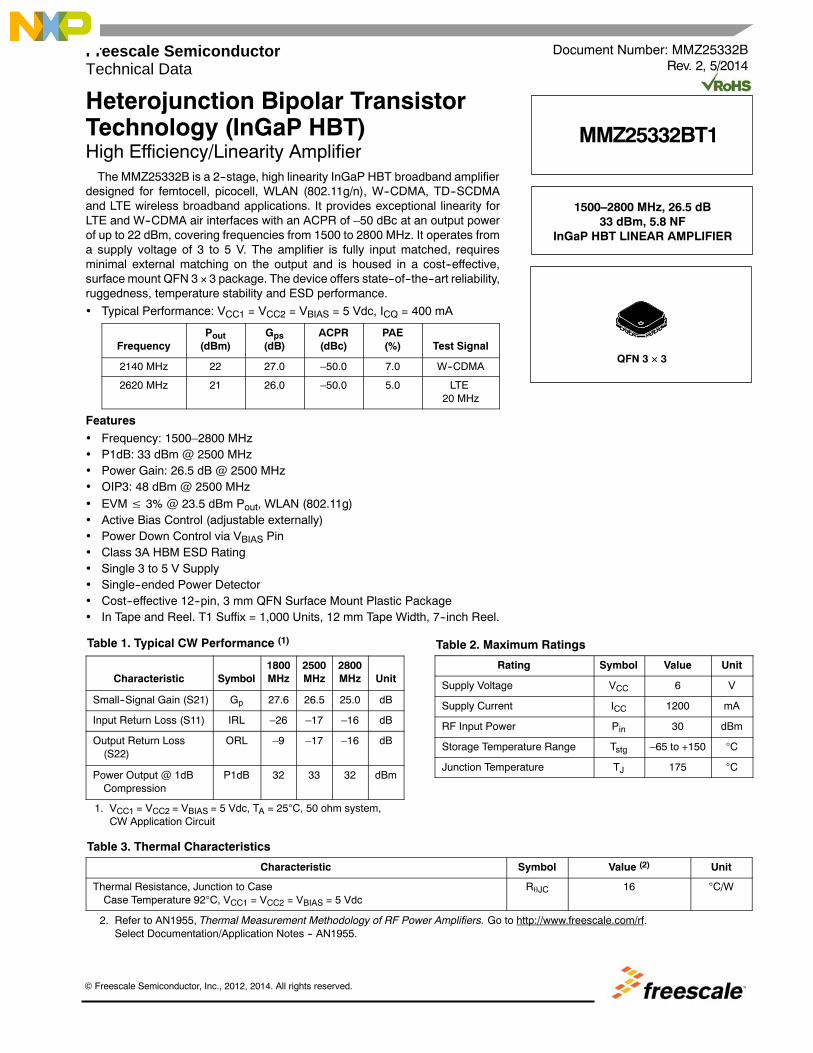
Heterojunction Bipolar Transistor Technology (InGaP HBT) High Efficiency/Linearity Amplifier The MMZ25332B is a 2--stage, high linearity InGaP HBT broadband amplifier designed for femtocell, picocell, WLAN (802.11g/n), W--CDMA, TD--SCDMA and LTE wireless broadband applications. It provides exceptional linearity for LTE and W--CDMA air interfaces with an ACPR of –50 dBc at an output power of up to 22 dBm, covering frequencies from 1500 to 2800 MHz. It operates from a supply voltage of 3 to 5 V. The amplifier is fully input matched, requires minimal external matching on the output and is housed in a cost--effective, surface mount QFN 3 × 3 package. The device offers state--of--the--art reliability, ruggedness, temperature stability and ESD performance. • Typical Performance: V CC1 =V CC2 =V BIAS = 5 Vdc, I CQ = 400 mA Frequency P out (dBm) G ps (dB) ACPR (dBc) PAE (%) Test Signal 2140 MHz 22 27.0 –50.0 7.0 W--CDMA 2620 MHz 21 26.0 –50.0 5.0 LTE 20 MHz Features • Frequency: 1500–2800 MHz • P1dB: 33 dBm @ 2500 MHz • Power Gain: 26.5 dB @ 2500 MHz • OIP3: 48 dBm @ 2500 MHz • EVM ≤ 3% @ 23.5 dBm P out , WLAN (802.11g) • Active Bias Control (adjustable externally) • Power Down Control via V BIAS Pin • Class 3A HBM ESD Rating • Single 3 to 5 V Supply • Single--ended Power Detector • Cost--effective 12--pin, 3 mm QFN Surface Mount Plastic Package • In Tape and Reel. T1 Suffix = 1,000 Units, 12 mm Tape Width, 7--inch Reel. Table 1. Typical CW Performance (1) Characteristic Symbol 1800 MHz 2500 MHz 2800 MHz Unit Small--Signal Gain (S21) G p 27.6 26.5 25.0 dB Input Return Loss (S11) IRL –26 –17 –16 dB Output Return Loss (S22) ORL –9 –17 –16 dB Power Output @ 1dB Compression P1dB 32 33 32 dBm 1. V CC1 =V CC2 =V BIAS = 5 Vdc, T A = 25°C, 50 ohm system, CW Application Circuit Table 2. Maximum Ratings Rating Symbol Value Unit Supply Voltage V CC 6 V Supply Current I CC 1200 mA RF Input Power P in 30 dBm Storage Temperature Range T stg –65 to +150 °C Junction Temperature T J 175 °C Table 3. Thermal Characteristics Characteristic Symbol Value (2) Unit Thermal Resistance, Junction to Case Case Temperature 92°C, V CC1 =V CC2 =V BIAS = 5 Vdc R θJC 16 °C/W 2. Refer to AN1955, Thermal Measurement Methodology of RF Power Amplifiers. Go to http://www.freescale.com/rf . Select Documentation/Application Notes -- AN1955. Freescale Semiconductor Technical Data Document Number: MMZ25332B Rev. 2, 5/2014 1500–2800 MHz, 26.5 dB 33 dBm, 5.8 NF InGaP HBT LINEAR AMPLIFIER MMZ25332BT1 QFN 3 × 3 © Freescale Semiconductor, Inc., 2012, 2014. All rights reserved.
Transcript of Freescale Semiconductor Document Number: MMZ25332B...
MMZ25332BT1
1RF Device DataFreescale Semiconductor, Inc.
Heterojunction Bipolar TransistorTechnology (InGaP HBT)High Efficiency/Linearity AmplifierThe MMZ25332B is a 2--stage, high linearity InGaP HBT broadband amplifier
designed for femtocell, picocell, WLAN (802.11g/n), W--CDMA, TD--SCDMAand LTE wireless broadband applications. It provides exceptional linearity forLTE and W--CDMA air interfaces with an ACPR of –50 dBc at an output powerof up to 22 dBm, covering frequencies from 1500 to 2800 MHz. It operates froma supply voltage of 3 to 5 V. The amplifier is fully input matched, requiresminimal external matching on the output and is housed in a cost--effective,surface mount QFN 3 × 3 package. The device offers state--of--the--art reliability,ruggedness, temperature stability and ESD performance.
• Typical Performance: VCC1 = VCC2 = VBIAS = 5 Vdc, ICQ = 400 mA
FrequencyPout(dBm)
Gps(dB)
ACPR(dBc)
PAE(%) Test Signal
2140 MHz 22 27.0 –50.0 7.0 W--CDMA
2620 MHz 21 26.0 –50.0 5.0 LTE20 MHz
Features• Frequency: 1500–2800 MHz• P1dB: 33 dBm @ 2500 MHz• Power Gain: 26.5 dB @ 2500 MHz• OIP3: 48 dBm @ 2500 MHz• EVM≤ 3% @ 23.5 dBm Pout, WLAN (802.11g)• Active Bias Control (adjustable externally)• Power Down Control via VBIAS Pin• Class 3A HBM ESD Rating• Single 3 to 5 V Supply• Single--ended Power Detector• Cost--effective 12--pin, 3 mm QFN Surface Mount Plastic Package• In Tape and Reel. T1 Suffix = 1,000 Units, 12 mm Tape Width, 7--inch Reel.
Table 1. Typical CW Performance (1)
Characteristic Symbol1800MHz
2500MHz
2800MHz Unit
Small--Signal Gain (S21) Gp 27.6 26.5 25.0 dB
Input Return Loss (S11) IRL –26 –17 –16 dB
Output Return Loss(S22)
ORL –9 –17 –16 dB
Power Output @ 1dBCompression
P1dB 32 33 32 dBm
1. VCC1 = VCC2 = VBIAS = 5 Vdc, TA = 25°C, 50 ohm system,CW Application Circuit
Table 2. Maximum Ratings
Rating Symbol Value Unit
Supply Voltage VCC 6 V
Supply Current ICC 1200 mA
RF Input Power Pin 30 dBm
Storage Temperature Range Tstg –65 to +150 °C
Junction Temperature TJ 175 °C
Table 3. Thermal Characteristics
Characteristic Symbol Value (2) Unit
Thermal Resistance, Junction to CaseCase Temperature 92°C, VCC1 = VCC2 = VBIAS = 5 Vdc
RθJC 16 °C/W
2. Refer to AN1955, Thermal Measurement Methodology of RF Power Amplifiers. Go to http://www.freescale.com/rf.Select Documentation/Application Notes -- AN1955.
Freescale SemiconductorTechnical Data
Document Number: MMZ25332BRev. 2, 5/2014
1500–2800 MHz, 26.5 dB33 dBm, 5.8 NF
InGaP HBT LINEAR AMPLIFIER
MMZ25332BT1
QFN 3 × 3
© Freescale Semiconductor, Inc., 2012, 2014. All rights reserved.
2RF Device Data
Freescale Semiconductor, Inc.
MMZ25332BT1
Table 4. Electrical Characteristics(1) (VCC1 = VCC2 = VBIAS = 5 Vdc, 2500 MHz, TA = 25°C, 50 ohm system, in Freescale CWApplication Circuit)
Characteristic Symbol Min Typ Max Unit
Small--Signal Gain (S21) Gp 25 26.5 — dB
Input Return Loss (S11) IRL — –17 — dB
Output Return Loss (S22) ORL — –17 — dB
Power Output @ 1dB Compression P1dB — 33 — dBm
Third Order Output Intercept Point, Two--Tone CW OIP3 — 48 — dBm
Noise Figure NF — 5.8 — dB
Supply Current ICQ 356 390 412 mA
Supply Voltage VCC — 5 — V
Table 5. ESD Protection Characteristics
Test Methodology Class
Human Body Model (per JESD22--A114) 3A
Machine Model (per EIA/JESD22--A115) B
Charge Device Model (per JESD22--C101) IV
Table 6. Moisture Sensitivity Level
Test Methodology Rating Package Peak Temperature Unit
Per JESD22--A113, IPC/JEDEC J--STD--020 1 260 °C
1. See Appendix A for test fixture documentation.
Figure 1. Functional Block Diagram Figure 2. Pin Connections
VCC1
VCC2/RFout
RFin
1 9
2 8
3 7
12 11 10
4 5 6
VCC2/RFout
VCC1 PDET
N.C.
RFin
VCC2/RFout
VBA1 VBA2 VBIAS
VCC1
VCC2/RFout
RFin
VCC2/RFout
VCC1 PDET
RFin
VCC2/RFout
VBA1 VBIASVBA2
BIASCIRCUIT
MMZ25332BT1
3RF Device DataFreescale Semiconductor, Inc.
50 OHM APPLICATION CIRCUIT: 2110–2170 MHz, 5 VOLT OPERATION
Figure 3. MMZ25332BT1 Test Circuit Schematic
R1
L1
C12
3
1
C4
BIAS CIRCUIT
VCC1
Z1
L2
VBIAS
C1
2
R2
PDET
C3
C9
VCC2
C13
C14
C6
Z1 0.151″ × 0.030″ Microstrip
RFINPUT
RFOUTPUT
4 5 6
7
8
9
12 11 10
Table 7. MMZ25332BT1 Test Circuit Component Designations and ValuesPart Description Part Number Manufacturer
C1, C12 1 μF Chip Capacitors GRM155R61A105KE15 Murata
C2, C5, C7, C8, C10, C11,C15
Components Not Placed
C3 470 pF Chip Capacitor GRM1555C1H471JA01 Murata
C4 8.2 pF Chip Capacitor 04023J8R2BBS AVX
C6 4.7 μF Chip Capacitor GRM188R60J475KE19D Murata
C9, C14 22 pF Chip Capacitors 04023J22R0BBS AVX
C13 3.3 pF Chip Capacitor 04023J3R3BBS AVX
L1 12 nH Chip Inductor 0603HC--12NXJLW Coilcraft
L2 6.8 nH Chip Inductor 0603HC--6N8XJLW Coilcraft
R1 1.2 kΩ, 1/16 W Chip Resistor RC0402JR--071K2L Yageo
R2 330 Ω, 1/16 W Chip Resistor RC0402JR--07330L Yageo
PCB 0.014″, εr = 3.7 FR408 Isola
Note: Component numbers C2, C5, C7, C8, C10, C11 and C15 are labeled on board but not placed.

4RF Device Data
Freescale Semiconductor, Inc.
MMZ25332BT1
50 OHM APPLICATION CIRCUIT: 2110–2170 MHz, 5 VOLT OPERATION
Figure 4. MMZ25332BT1 Test Circuit Component Layout
(1) VBIAS [Board] supplies VBA1, VBA2 and VBIAS [Device].Note: Component numbers C2*, C5*, C7*, C8*, C10*, C11* and C15* are labeled on board but not placed.
C9
C7*
R1 C12R2
C13 C15* C14
C6
C1
L1
C4
L2
C3
QFN 3×3--12HRev. 1
RFOUTRFIN
C2*
C5*
C10*
C8*C11*
VCC1
VDECT
VCC2
VBIAS (1)
PCB actual size: 1.3″ × 1.46″.
Table 7. MMZ25332BT1 Test Circuit Component Designations and ValuesPart Description Part Number Manufacturer
C1, C12 1 μF Chip Capacitors GRM155R61A105KE15 Murata
C2, C5, C7, C8, C10, C11,C15
Components Not Placed
C3 470 pF Chip Capacitor GRM1555C1H471JA01 Murata
C4 8.2 pF Chip Capacitor 04023J8R2BBS AVX
C6 4.7 μF Chip Capacitor GRM188R60J475KE19D Murata
C9, C14 22 pF Chip Capacitors 04023J22R0BBS AVX
C13 3.3 pF Chip Capacitor 04023J3R3BBS AVX
L1 12 nH Chip Inductor 0603HC--12NXJLW Coilcraft
L2 6.8 nH Chip Inductor 0603HC--6N8XJLW Coilcraft
R1 1.2 kΩ, 1/16 W Chip Resistor RC0402JR--071K2L Yageo
R2 330 Ω, 1/16 W Chip Resistor RC0402JR--07330L Yageo
PCB 0.014″, εr = 3.7 FR408 Isola
(Test Circuit Component Designations and Values table repeated for reference.)
MMZ25332BT1
5RF Device DataFreescale Semiconductor, Inc.
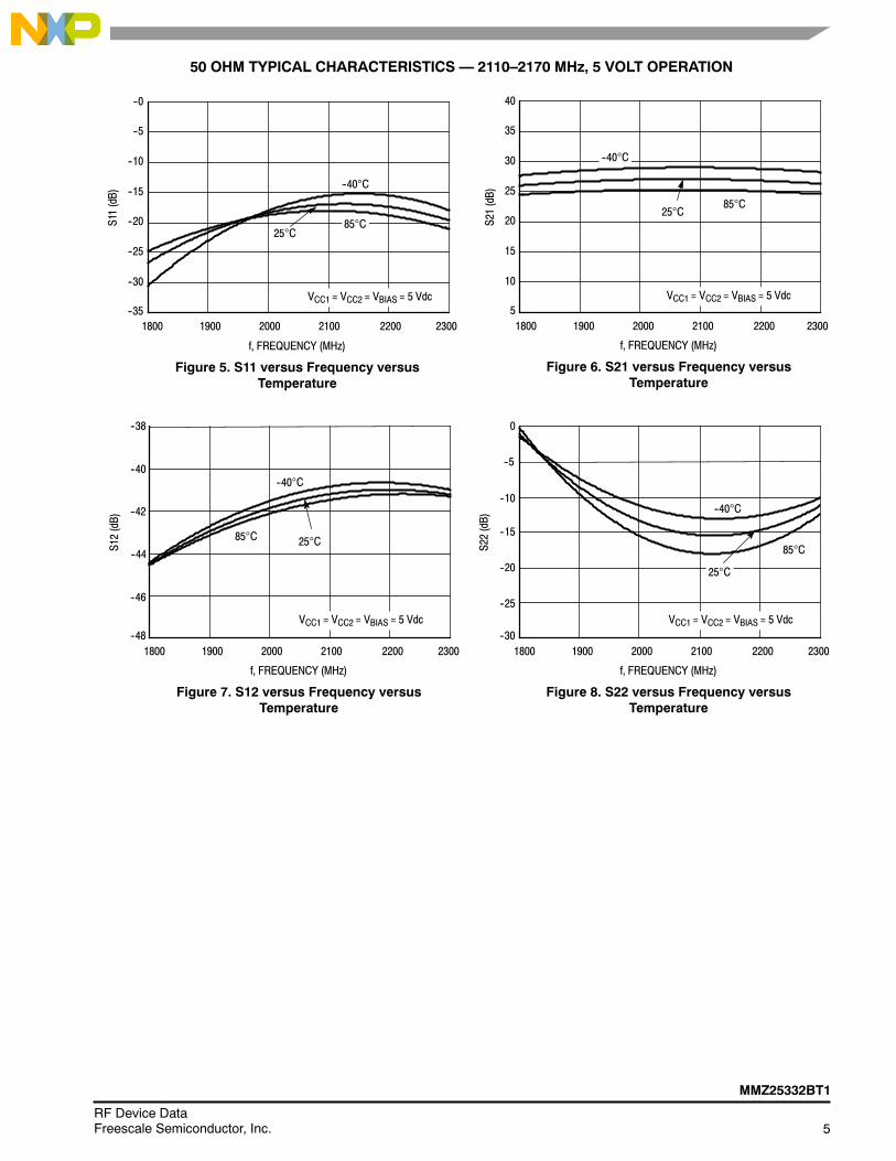
50 OHM TYPICAL CHARACTERISTICS — 2110–2170 MHz, 5 VOLT OPERATION
--30
--20
Figure 5. S11 versus Frequency versusTemperature
2300--35
--0
1800
f, FREQUENCY (MHz)
1900
--5
--10
--15
--20
--25
--30
S11(dB)
--40°C
2000 2100 2200
25°C85°C
Figure 6. S21 versus Frequency versusTemperature
5
40
f, FREQUENCY (MHz)
35
30
25
15
10
S21(dB)
--40°C
25°C85°C
Figure 7. S12 versus Frequency versusTemperature
--48
--38
f, FREQUENCY (MHz)
--40
--42
--46
S12(dB)
--40°C
25°C85°C
VCC1 = VCC2 = VBIAS = 5 Vdc VCC1 = VCC2 = VBIAS = 5 Vdc
VCC1 = VCC2 = VBIAS = 5 Vdc
20
Figure 8. S22 versus Frequency versusTemperature
0
f, FREQUENCY (MHz)
--5
--10
--15
--25
S22(dB)
--40°C
25°C
85°C
VCC1 = VCC2 = VBIAS = 5 Vdc
23001800 1900 2000 2100 2200
23001800 1900 2000 2100 2200 23001800 1900 2000 2100 2200
--44
6RF Device Data
Freescale Semiconductor, Inc.
MMZ25332BT1
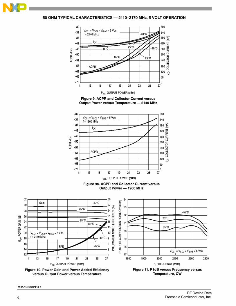
50 OHM TYPICAL CHARACTERISTICS — 2110–2170 MHz, 5 VOLT OPERATION
540
120
180
Figure 9. ACPR and Collector Current versusOutput Power versus Temperature — 2140 MHz
Pout, OUTPUT POWER (dBm)
--30
--34
--38
--62
21
--50
I CC,COLLECTORCURRENT(mA)
ACPR
(dBc)
--42
--58
11 13
240
420
480
--54
--66
27
600
0
--46
15 17 19 2523
--40°C
25°C
85°C 25°C
85°C
--40°C
85°C85°C
Gain
PAE
ICC
--70
VCC1 = VCC2 = VBIAS = 5 Vdcf = 2140 MHz
VCC1 = VCC2 = VBIAS = 5 Vdcf = 2140 MHz
--30
--34
--38
--62
21
--50
--42
--58
11 13
300
360
--54
--66
27
60
--46
15 17 19 2523--70
540
120
180
Figure 9a. ACPR and Collector Current versusOutput Power — 1960 MHz
Pout, OUTPUT POWER (dBm)
--30
--34
--38
--62
21
--50
I CC,COLLECTORCURRENT(mA)
ACPR
(dBc)
--42
--58
11 13
300
360
480
--54
--66
27
600
0
--46
15 17 19 2523
ACPR
ICC
--70
VCC1 = VCC2 = VBIAS = 5 Vdcf = 1960 MHz
Pout, OUTPUT POWER (dBm)
--30
--34
--38
--62
21
--50
--42
--58
11 13
240
420
--54
--66
27
60
--46
15 17 19 2523--70
27
6
9
Figure 10. Power Gain and Power Added Efficiencyversus Output Power versus Temperature
Pout, OUTPUT POWER (dBm)
30
28
26
14
21
20
PAE,POWER
ADDED
EFFICIENCY(%)
Gps,POWER
GAIN(dB)
24
16
11 13
12
15
18
21
24
18
1227
30
3
0
22
15 17 19 2523
32
Figure 11. P1dB versus Frequency versusTemperature, CW
f, FREQUENCY (MHz)
33
32
31
28
30
27
29
--40°C
25°C
85°C
34
P1dB,1dB
COMPRESSIONPOINT,CW(dBm
)
23001800 1900 2000 2100 2200
--40°C
--40°C
25°C
25°C
ACPR
VCC1 = VCC2 = VBIAS = 5 Vdc

MMZ25332BT1
7RF Device DataFreescale Semiconductor, Inc.
50 OHM TYPICAL CHARACTERISTICS — 2110–2170 MHz, 5 VOLT OPERATION
27
6
9
--30
--34
--38
--62
21
--50
PAE,POWER
ADDED
EFFICIENCY(%)
ACPR
(dBc)
--42
--58
11 13
12
15
18
21
24
--54
--66
27
30
3
0
--46
15 17 19 2523--70
Pout, OUTPUT POWER (dBm)
--30
--34
--38
--62
23
--50
ACPR
(dBc)
--42
--58
17
--54
--66
27
--46
19 21 25--70
PAE
1.8
1.6
1.4
0.2
21
0.8
P DET,POWER
DETECTOR(V)
1.2
0.4
11 13
0.6
027
1
15 17 19 2523
25°C
85°C
--40°C
2VCC1 = VCC2 = VBIAS = 5 Vdcf = 2140 MHz
Pout, OUTPUT POWER (dBm)
Figure 12. Power Detector versus Output Powerversus Temperature
Figure 13. ACPR and Power Added Efficiencyversus Output Power
Pout, OUTPUT POWER (dBm)
Figure 14. ACPR versus Output Power withBias Config 2 Uncorrected and Bias Config 2
DPD Corrected
Note: Bias Config 1: 400 mA Avg. using R2 = 330 Ω
Bias Config 2: 300 mA Avg. using R2 = 470 Ω
VCC1 = VCC2 = VBIAS = 5 Vdcf = 2140 MHzBias Config 2 = 300 mA Avg.
Bias Config 1
Note: Bias Config 2: 300 mA Avg. using R2 = 470 Ω
Uncorrected
DPD Corrected, with Memory Correction
ACPR
VCC1 = VCC2 = VBIAS = 5 Vdc, f = 2140 MHzBias Config 1 = 400 mA Avg.Bias Config 2 = 300 mA Avg.
Bias Config 2
Bias Config 1
Bias Config 2
8RF Device Data
Freescale Semiconductor, Inc.
MMZ25332BT1
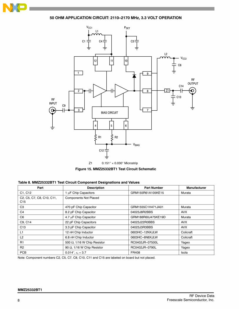
50 OHM APPLICATION CIRCUIT: 2110–2170 MHz, 3.3 VOLT OPERATION
Figure 15. MMZ25332BT1 Test Circuit Schematic
R1
L1
C12
3
1
C4
BIAS CIRCUIT
VCC1
Z1
L2
VBIAS
C1
2
R2
PDET
C3
C9
VCC2
C13
C14
C6
Z1 0.151″ × 0.030″ Microstrip
RFINPUT
RFOUTPUT
4 5 6
7
8
9
12 11 10
Table 8. MMZ25332BT1 Test Circuit Component Designations and ValuesPart Description Part Number Manufacturer
C1, C12 1 μF Chip Capacitors GRM155R61A105KE15 Murata
C2, C5, C7, C8, C10, C11,C15
Components Not Placed
C3 470 pF Chip Capacitor GRM1555C1H471JA01 Murata
C4 8.2 pF Chip Capacitor 04023J8R2BBS AVX
C6 4.7 μF Chip Capacitor GRM188R60J475KE19D Murata
C9, C14 22 pF Chip Capacitors 04023J22R0BBS AVX
C13 3.3 pF Chip Capacitor 04023J3R3BBS AVX
L1 12 nH Chip Inductor 0603HC--12NXJLW Coilcraft
L2 6.8 nH Chip Inductor 0603HC--6N8XJLW Coilcraft
R1 500 Ω, 1/16 W Chip Resistor RC0402JR--07500L Yageo
R2 90 Ω, 1/16 W Chip Resistor RC0402JR--0790L Yageo
PCB 0.014″, εr = 3.7 FR408 Isola
Note: Component numbers C2, C5, C7, C8, C10, C11 and C15 are labeled on board but not placed.

MMZ25332BT1
9RF Device DataFreescale Semiconductor, Inc.
50 OHM APPLICATION CIRCUIT: 2110–2170 MHz, 3.3 VOLT OPERATION
Figure 16. MMZ25332BT1 Test Circuit Component Layout
(1) VBIAS [Board] supplies VBA1, VBA2 and VBIAS [Device].Note: Component numbers C2*, C5*, C7*, C8*, C10*, C11* and C15* are labeled on board but not placed.
C9
C7*
R1 C12R2
C13 C15* C14
C6
C1
L1
C4
L2
C3
QFN 3×3--12HRev. 1
RFOUTRFIN
C2*
C5*
C10*
C8*C11*
VCC1
VDECT
VCC2
VBIAS (1)
PCB actual size: 1.3″ × 1.46″.
Table 8. MMZ25332BT1 Test Circuit Component Designations and ValuesPart Description Part Number Manufacturer
C1, C12 1 μF Chip Capacitors GRM155R61A105KE15 Murata
C2, C5, C7, C8, C10, C11,C15
Components Not Placed
C3 470 pF Chip Capacitor GRM1555C1H471JA01 Murata
C4 8.2 pF Chip Capacitor 04023J8R2BBS AVX
C6 4.7 μF Chip Capacitor GRM188R60J475KE19D Murata
C9, C14 22 pF Chip Capacitors 04023J22R0BBS AVX
C13 3.3 pF Chip Capacitor 04023J3R3BBS AVX
L1 12 nH Chip Inductor 0603HC--12NXJLW Coilcraft
L2 6.8 nH Chip Inductor 0603HC--6N8XJLW Coilcraft
R1 500 Ω, 1/16 W Chip Resistor RC0402JR--07500L Yageo
R2 90 Ω, 1/16 W Chip Resistor RC0402JR--0790L Yageo
PCB 0.014″, εr = 3.7 FR408 Isola
(Test Circuit Component Designations and Values table repeated for reference.)
10RF Device Data
Freescale Semiconductor, Inc.
MMZ25332BT1
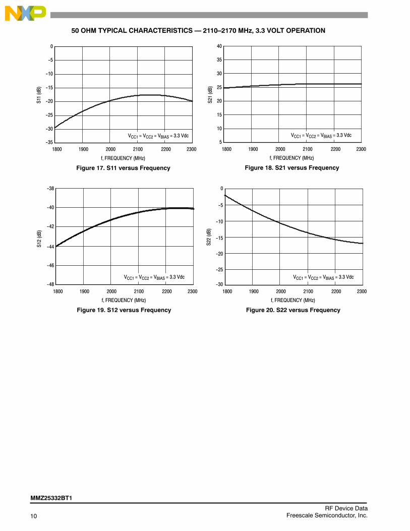
50 OHM TYPICAL CHARACTERISTICS — 2110–2170 MHz, 3.3 VOLT OPERATION
--30
Figure 17. S11 versus Frequency
2300--35
0
1800
f, FREQUENCY (MHz)
1900
--5
--10
--15
--20
--25
--30
S11(dB)
2000 2100 2200
Figure 18. S21 versus Frequency
5
40
f, FREQUENCY (MHz)
35
30
25
15
10
S21(dB)
Figure 19. S12 versus Frequency
--48
--38
f, FREQUENCY (MHz)
--40
--42
--44
--46
S12(dB)
VCC1 = VCC2 = VBIAS = 3.3 Vdc VCC1 = VCC2 = VBIAS = 3.3 Vdc
VCC1 = VCC2 = VBIAS = 3.3 Vdc
20
Figure 20. S22 versus Frequency
0
f, FREQUENCY (MHz)
--5
--10
--15
--20
--25
S22(dB)
VCC1 = VCC2 = VBIAS = 3.3 Vdc
23001800 1900 2000 2100 2200
23001800 1900 2000 2100 2200 23001800 1900 2000 2100 2200
MMZ25332BT1
11RF Device DataFreescale Semiconductor, Inc.
50 OHM TYPICAL CHARACTERISTICS — 2110–2170 MHz, 3.3 VOLT OPERATION
540
120
180
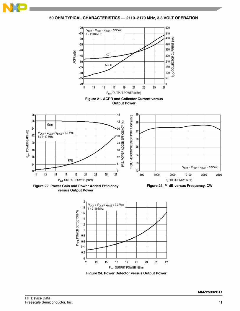
Figure 21. ACPR and Collector Current versusOutput Power
Pout, OUTPUT POWER (dBm)
--20
--25
--30
--60
21
--45
I CC,COLLECTORCURRENT(mA)
ACPR
(dBc)
--35
--55
11 13
240
300
360
420
480
--50
--65
27
600
60
0
--40
15 17 19 2523
ACPR
42
12
Figure 22. Power Gain and Power Added Efficiencyversus Output Power
Pout, OUTPUT POWER (dBm)
26
24
14
21
18
PAE,POWER
ADDED
EFFICIENCY(%)
Gps,POWER
GAIN(dB)
22
11 13
18
24
30
36
16
1227
48
6
0
20
15 17 19 2523
28
Gain
PAE
Figure 23. P1dB versus Frequency, CW
f, FREQUENCY (MHz)
28
27
26
23
25
22
24
29
P1dB,1dB
COMPRESSIONPOINT,CW(dBm
)
ICC
VCC1 = VCC2 = VBIAS = 3.3 Vdc
--70
VCC1 = VCC2 = VBIAS = 3.3 Vdcf = 2140 MHz
VCC1 = VCC2 = VBIAS = 3.3 Vdcf = 2140 MHz
Figure 24. Power Detector versus Output Power
Pout, OUTPUT POWER (dBm)
1.8
1.6
1.4
0.2
21
0.8
P DET,POWER
DETECTOR(V)
1.2
0.4
11 13
0.6
027
1
15 17 19 2523
2
23001800 1900 2000 2100 2200
VCC1 = VCC2 = VBIAS = 3.3 Vdcf = 2140 MHz
12RF Device Data
Freescale Semiconductor, Inc.
MMZ25332BT1
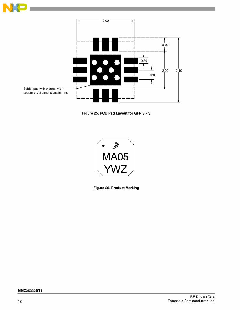
Figure 25. PCB Pad Layout for QFN 3 × 3
3.00
3.402.000.50
0.30
0.70
Solder pad with thermal viastructure. All dimensions in mm.
Figure 26. Product Marking
MA05YWZ

MMZ25332BT1
13RF Device DataFreescale Semiconductor, Inc.
PACKAGE DIMENSIONS

14RF Device Data
Freescale Semiconductor, Inc.
MMZ25332BT1
MMZ25332BT1
15RF Device DataFreescale Semiconductor, Inc.
16RF Device Data
Freescale Semiconductor, Inc.
MMZ25332BT1
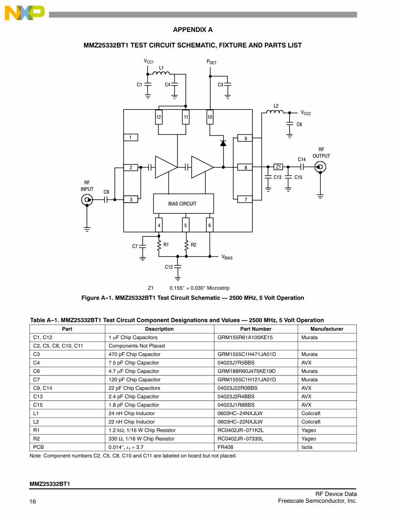
APPENDIX A
MMZ25332BT1 TEST CIRCUIT SCHEMATIC, FIXTURE AND PARTS LIST
Figure A--1. MMZ25332BT1 Test Circuit Schematic — 2500 MHz, 5 Volt Operation
R1
L1
C12
3
1
C4
BIAS CIRCUIT
VCC1
Z1
L2
VBIAS
C1
2
R2
PDET
C3
C9
C7
VCC2
C13 C15
C14
C6
Z1 0.155″ × 0.030″ Microstrip
RFINPUT
RFOUTPUT
4 5 6
7
8
9
12 11 10
Table A--1. MMZ25332BT1 Test Circuit Component Designations and Values — 2500 MHz, 5 Volt OperationPart Description Part Number Manufacturer
C1, C12 1 μF Chip Capacitors GRM155R61A105KE15 Murata
C2, C5, C8, C10, C11 Components Not Placed
C3 470 pF Chip Capacitor GRM1555C1H471JA01D Murata
C4 7.5 pF Chip Capacitor 04023J7R5BBS AVX
C6 4.7 μF Chip Capacitor GRM188R60J475KE19D Murata
C7 120 pF Chip Capacitor GRM1555C1H121JA01D Murata
C9, C14 22 pF Chip Capacitors 04023J22R0BBS AVX
C13 2.4 pF Chip Capacitor 04023J2R4BBS AVX
C15 1.8 pF Chip Capacitor 04023J1R8BBS AVX
L1 24 nH Chip Inductor 0603HC--24NXJLW Coilcraft
L2 22 nH Chip Inductor 0603HC--22NXJLW Coilcraft
R1 1.2 kΩ, 1/16 W Chip Resistor RC0402JR--071K2L Yageo
R2 330 Ω, 1/16 W Chip Resistor RC0402JR--07330L Yageo
PCB 0.014″, εr = 3.7 FR408 Isola
Note: Component numbers C2, C5, C8, C10 and C11 are labeled on board but not placed.
MMZ25332BT1
17RF Device DataFreescale Semiconductor, Inc.
Appendix A (continued)
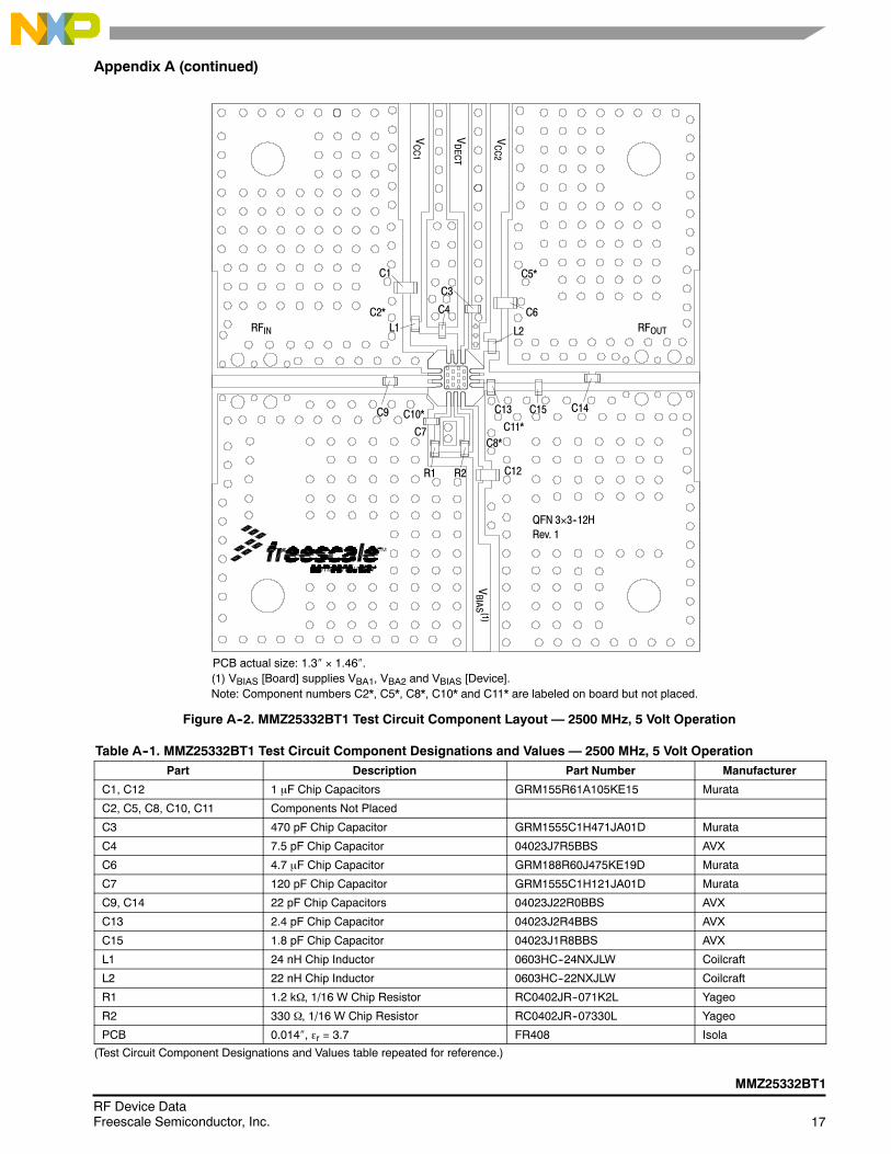
Figure A--2. MMZ25332BT1 Test Circuit Component Layout — 2500 MHz, 5 Volt Operation
(1) VBIAS [Board] supplies VBA1, VBA2 and VBIAS [Device].Note: Component numbers C2*, C5*, C8*, C10* and C11* are labeled on board but not placed.
C9
C7
R1 C12R2
C13 C15 C14
C6
C1
L1
C4
L2
C3
QFN 3×3--12HRev. 1
RFOUTRFIN
C2*
C5*
C10*
C8*C11*
VCC1
VDECT
VCC2
VBIAS (1)
PCB actual size: 1.3″ × 1.46″.
Table A--1. MMZ25332BT1 Test Circuit Component Designations and Values — 2500 MHz, 5 Volt OperationPart Description Part Number Manufacturer
C1, C12 1 μF Chip Capacitors GRM155R61A105KE15 Murata
C2, C5, C8, C10, C11 Components Not Placed
C3 470 pF Chip Capacitor GRM1555C1H471JA01D Murata
C4 7.5 pF Chip Capacitor 04023J7R5BBS AVX
C6 4.7 μF Chip Capacitor GRM188R60J475KE19D Murata
C7 120 pF Chip Capacitor GRM1555C1H121JA01D Murata
C9, C14 22 pF Chip Capacitors 04023J22R0BBS AVX
C13 2.4 pF Chip Capacitor 04023J2R4BBS AVX
C15 1.8 pF Chip Capacitor 04023J1R8BBS AVX
L1 24 nH Chip Inductor 0603HC--24NXJLW Coilcraft
L2 22 nH Chip Inductor 0603HC--22NXJLW Coilcraft
R1 1.2 kΩ, 1/16 W Chip Resistor RC0402JR--071K2L Yageo
R2 330 Ω, 1/16 W Chip Resistor RC0402JR--07330L Yageo
PCB 0.014″, εr = 3.7 FR408 Isola
(Test Circuit Component Designations and Values table repeated for reference.)
18RF Device Data
Freescale Semiconductor, Inc.
MMZ25332BT1
PRODUCT DOCUMENTATION, SOFTWARE AND TOOLS
Refer to the following documents, software and tools to aid your design process.
Application Notes• AN1955: Thermal Measurement Methodology of RF Power Amplifiers
Software• .s2p File
Development Tools• Printed Circuit Boards
For Software and Tools, do a Part Number search at http://www.freescale.com, and select the “Part Number” link. Go to theSoftware & Tools tab on the part’s Product Summary page to download the respective tool.
FAILURE ANALYSIS
At this time, because of the physical characteristics of the part, failure analysis is limited to electrical signature analysis. Incases where Freescale is contractually obligated to perform failure analysis (FA) services, full FA may be performed by thirdparty vendors with moderate success. For updates contact your local Freescale Sales Office.
REVISION HISTORY
The following table summarizes revisions to this document.
Revision Date Description
0 May 2012 • Initial Release of Data Sheet
1 Dec. 2012 • Added 2140 MHz, 5 Volt Operation, as follows:-- Fig. 3, Test Circuit Schematic, p. 3-- Table 7, Test Circuit Component Designations and Values, p. 3-- Fig. 4, Test Circuit Component Layout, p. 4-- Fig. 5, S11 versus Frequency versus Temperature, p. 5-- Fig. 6, S21 versus Frequency versus Temperature, p. 5-- Fig. 7, S12 versus Frequency versus Temperature, p. 5-- Fig. 8, S22 versus Frequency versus Temperature, p. 5-- Fig. 9. ACPR and Collector Current versus Output Power versus Temperature — 2140 MHz, p.6-- Fig. 9a. ACPR and Collector Current versus Output Power — 1960 MHz, p.6-- Fig. 10. Power Gain and Power Added Efficiency versus Output Power versus Temperature, p. 6-- Fig. 11. P1dB versus Frequency versus Temperature, CW, p. 6-- Fig. 12. Power Detector versus Output Power versus Temperature, p. 7-- Fig. 13. ACPR and Power Added Efficiency versus Output Power, p. 7-- Fig. 14. ACPR versus Output Power with Bias Config 2 Uncorrected and Bias Config 2 DPD Corrected,p. 7
• Added 2140 MHz, 3.3 Volt Operation, as follows:-- Fig. 15, Test Circuit Schematic, p. 8-- Table 8, Test Circuit Component Designations and Values, p. 8-- Fig. 16, Test Circuit Component Layout, p. 9-- Fig. 17, S11 versus Frequency versus Temperature, p. 10-- Fig. 18, S21 versus Frequency versus Temperature, p. 10-- Fig. 19, S12 versus Frequency versus Temperature, p. 10-- Fig. 20, S22 versus Frequency versus Temperature, p. 10-- Fig. 21, ACPR and Collector Current versus Output Power, p .11-- Fig. 22, Power Gain and Power Added Efficiency versus Output Power, p. 11-- Fig. 23, P1dB versus Frequency, CW, p. 11-- Fig. 24, Power Detector versus Output Power, p. 11
• Added Appendix A, Test Circuit Schematic, Fixture and Parts List (for 2500 MHz, 5 Volt Operation) asfollows:-- Moved former Fig. 3 (now Fig. 27), Test Circuit Schematic, to p. 16-- Moved former Table 7 (now Table 9), Test Circuit Component Designations and Values, to p.16-- Moved former Fig. 4 (now Fig. 28), Test Circuit Component Layout, to p.17
2 May 2014 • Updated frequency from 1800--2800 MHz to 1500--2800 MHz and Junction Temperature from 150°C to175°C to reflect recent test results of the device, p. 1
• Added Failure Analysis information, p. 18
MMZ25332BT1
19RF Device DataFreescale Semiconductor, Inc.
Information in this document is provided solely to enable system and softwareimplementers to use Freescale products. There are no express or implied copyrightlicenses granted hereunder to design or fabricate any integrated circuits based on theinformation in this document.
Freescale reserves the right to make changes without further notice to any productsherein. Freescale makes no warranty, representation, or guarantee regarding thesuitability of its products for any particular purpose, nor does Freescale assume anyliability arising out of the application or use of any product or circuit, and specificallydisclaims any and all liability, including without limitation consequential or incidentaldamages. “Typical” parameters that may be provided in Freescale data sheets and/orspecifications can and do vary in different applications, and actual performance mayvary over time. All operating parameters, including “typicals,” must be validated foreach customer application by customer’s technical experts. Freescale does not conveyany license under its patent rights nor the rights of others. Freescale sells productspursuant to standard terms and conditions of sale, which can be found at the followingaddress: freescale.com/SalesTermsandConditions.
Freescale and the Freescale logo are trademarks of Freescale Semiconductor, Inc.,Reg. U.S. Pat. & Tm. Off. All other product or service names are the property of theirrespective owners.E 2012, 2014 Freescale Semiconductor, Inc.
How to Reach Us:
Home Page:freescale.com
Web Support:freescale.com/support
Document Number: MMZ25332BRev. 2, 5/2014