A new system of digital circuit blocks for industrial ... Bound... · A new system of digital...
7
164 PHILlPS TECHNICAL REVIEW VOLUME26 A new system of digital circuit blocks for industrial measuring and control equipment [*1 D. Gossel, G. Kaps and W. Schott Introduetion The characteristic of digital information processing installations is that in their construction a small group of basic circuits is used, each of which occurs in large numbers. The group of basic circuits is called a system. In order to enable designers to realize a given logical design without going into electronic details, several manufacturers have developed systems consisting of "And", "Or" and "Negation" circuit blocks as well as bistable circuits (flip-flops) for counting and storing purposes [11. Although it should be possible to realize any logical design using such a system, circuit limitations must be considered, and extensive load tables limit the possibil- ities of combining the various blocks. The number of prohibited combinations increases with the number of different blocks, making the load tables more and more complicated. Amplifiers for decoupling purposes - e.g. P-N-P and N-P-N emitter followers - have to be used, although they have no logical function, and this is at variance with the original aim [21. Consequently there are systems in which the total number of blocks required for a given problem bears no relation to the number that have a logic function. This influences not only costs, but .also reliability, since an increase in the number of blocks also causes an increase in the failure rate. Efforts have been made to avoid these difficulties by decreasing the number of basic circuits. Switching algebra provides a solution through the use of De Morgan's formula [31: Xl + X2 + .... + Xn = Xl • X2 ••••• Xn, xi . X2 ••••• Xn = xi + X2 +... + xn This formula gives the relationship between the AND and OR operation and the Negation. It may be seen from this that the one operation can always be replaced by the other together with the negation. The NAND and NOR techniques often used at ' present go another step further. Here it is possible by using suitable combinatieris of the AND operation t?gether with negation, or the OR operation together with negation, to make only one type ofblock suffice [41. Dipt-Ing. D. Gossel, iJipl.-Ing. G. Kaps and Dipt-Ing. W. Schoft are research workers at the Hamburg laboratory of Philips Zentra/laboratorium GmbH. 621.374.32 Fig. 1 shows the AND and OR operation realized with NAND- and NOR-blocks. Each NAND and NOR symbol represents one basic circuit containing at least one transistor together with resistors, capacitors and diodes. Q Fig. 1. Logic circuits for the OR operation and the AND opera- tion, built up of a) NAND circuits, b) NOR circuits. A second advantage of using only one type of block for all logical circuits is that the load tables in the NAND and NOR systems reduce to one single load rule. It is only necessary to know how many NAND or NOR circuits can be reliably controlled by a pre- vious NAND or NOR. There are no other forms of . loading. A serious disadvantage however is the large number of blocks to be used for certain operations. In order to realize an OR operation, one relativelyexpensiveNAND block is necessary for each input (fig. la). The AND [*1 Editorial note: An article by E. J. van Barneveld, Philips ICOMA Division, Eindhoven, will be appearing shortly in this journal, describing another systemof digital circuit blocks, designed for more universal use than the system presented here, and which is now being put into production by the ICOMA Division. '
Transcript of A new system of digital circuit blocks for industrial ... Bound... · A new system of digital...

164 PHILlPS TECHNICAL REVIEW VOLUME26
A new system of digital circuit blocksfor industrial measuring and control equipment [*1
D. Gossel, G. Kaps and W. Schott
Introduetion
The characteristic of digital information processinginstallations is that in their construction a small groupof basic circuits is used, each of which occurs in largenumbers. The group of basic circuits is called a system.In order to enable designers to realize a given logical
design without going into electronic details, severalmanufacturers have developed systems consisting of"And", "Or" and "Negation" circuit blocks as well asbistable circuits (flip-flops) for counting and storingpurposes [11.
Although it should be possible to realize any logicaldesign using such a system, circuit limitations must beconsidered, and extensive load tables limit the possibil-ities of combining the various blocks. The number ofprohibited combinations increases with the number ofdifferent blocks, making the load tables more and morecomplicated. Amplifiers for decoupling purposes - e.g.P-N-P and N-P-N emitter followers - have to be used,although they have no logical function, and this is atvariance with the original aim [21. Consequently thereare systems in which the total number of blocksrequired for a given problem bears no relation to thenumber that have a logic function. This influences notonly costs, but .also reliability, since an increase in thenumber of blocks also causes an increase in the failurerate.Efforts have been made to avoid these difficulties by
decreasing the number of basic circuits. Switchingalgebra provides a solution through the use of DeMorgan's formula [31:
Xl + X2 + ....+ Xn = Xl • X2 ••••• Xn,
xi . X2 ••••• Xn = xi + X2 + ... + xn·
This formula gives the relationship between the ANDand OR operation and the Negation. It may be seenfrom this that the one operation can always be replacedby the other together with the negation.The NAND and NOR techniques often used at '
present go another step further. Here it is possible byusing suitable combinatieris of the AND operationt?gether with negation, or the OR operation togetherwith negation, to make only one type ofblock suffice [41.
Dipt-Ing. D. Gossel, iJipl.-Ing. G. Kaps and Dipt-Ing. W. Schoftare research workers at the Hamburg laboratory of PhilipsZentra/laboratorium GmbH.
621.374.32
Fig. 1 shows the AND and OR operation realized withNAND- and NOR-blocks. Each NAND and NORsymbol represents one basic circuit containing at leastone transistor together with resistors, capacitors anddiodes.
Q
Fig. 1. Logic circuits for the OR operation and the AND opera-tion, built up of a) NAND circuits, b) NOR circuits.
A second advantage of using only one type of blockfor all logical circuits is that the load tables in theNAND and NOR systems reduce to one single loadrule. It is only necessary to know how many NANDor NOR circuits can be reliably controlled by a pre-vious NAND or NOR. There are no other forms of
. loading.A serious disadvantage however is the large number
of blocks to be used for certain operations. In order torealize an OR operation, one relatively expensiveNANDblock is necessary for each input (fig. la). The AND
[*1 Editorial note: An article by E. J. van Barneveld, PhilipsICOMA Division, Eindhoven, will be appearing shortly inthis journal, describing another systemof digital circuit blocks,designed for more universal use than the system presentedhere, and which is now being put into production by theICOMA Division. '

1965, No. 4/5/6
{)SySTEM or DIGITAL ClRCUlT BLOCKS 165
operation, however, can always be realized by twoNAND blocks regardless of the number of inputs(within certain limits). This also holds true when onlyNOR blocks are used; but in this case AND and ORoperations are exchanged (fig. lb) [51.
The new building-block system
The new system of digital circuit blocks described inthis paper. can be regarded as an attempt to reach agood compromise between these two methods. One ofthe characteristics of the new system is the use of onlytwo basic circuits, an active one, and a passive one.The active block contains a circuit in diode-transistorlogic (DTL). With the logic convention chosen("1" ,..... 12V, "0"""" 0 V) this block works as a NORcircuit (fig. 2). The passive block is an AND circuit(also called an AND gate) with two inputs (fig. 3).The number of inputs can within wide limits be in-creased by means of additional diodes. Using thepassive AND block it is not necessary to realize theAND operation with NOR blocks in the expensiveway shown in fig. lb.This building-block system which is especially
designed for industrial measurement and control pur-poses also has the following characteristics.1. There are no emitter followers. Only one type oftransistor and two types of diode are used.2. A standardized voltage supply is used (± 12 V± 5%). This value is considered a good compromisebetweena) a high voltage, giving low sensitivity to interference
and great freedom in combining various numbersand types of block - i.e. wide signal tolerances arepermitted -, and
b) a low voltage which suits the low maximum per-missible voltage for available transistors and giveslow dissipation.
3. The maximum switching frequency is 80 kc/s, themaximum counting frequency 30 kc/so (In some casesthe maximum counting frequency may be 80 kc/s.) Inindustrial applications the electronic circuits are mainlyused together with moving parts which have a certainmass. Experience here has shown that resolving power(accuracy) and speed call for a counting frequency of10 kc/s at the most. A frequency of 30 kc/s is thusadequate for quite extreme requirements.4. Asynchronous or synchronous modes of operationare optional. For simple problems involving low-speedcounting, the well-known asynchronous method maybe used. Here for example a bistable circuit is triggeredby a previous one which also has to supply the switch-ing energy. The maximum counting rate is determinedby the sum of the switching times of all stages and thusdecreases with an increasing -number of stages. The
maximum load per stage is much reduced in asynchron-ous counting techniques.
When somewhat higher demands are made, thesynchronous counting mode is to be preferred becauseof its great advantages, although a few more blocksare needed. Here all the stages of a counting circuitreceive switching pulses from a common clock-pulsegenerator. Each stage contains a separate signal input S,and the voltage applied to this input determines whetheror not a given clock pulse will trigger the circuit. Thismethod has the following consequences.a) The circuit is very insensitive to interference. As a
result of the delaying effect of the pulse gate con-trolled via the S input, parasitic pulses in the signalline will only be able to cause incorrect switching iftheir duration is > 5 (Ls, and their voltage-timeintegral is more than 60 (LVs, and the clock pulseis received more than 5 (Lsafter the start of a para-sitic pulse. Under normal conditions it is unlikelythat these three conditions will be satisfied simul-taneously. In practice therefore there will be almostno interference.
b) The various stages are not subjected to a dynamicload of any significance, since the triggering energyis supplied by the common clock-pulse generator.With the exception of the clock-pulse line, whichshould be as short and of as low capacity as possible,all signal lines are uncritical.
c) Unlimited use may be made ofthe maximum switch-ing frequency. All stages which have to be triggeredare prepared during the interval between two clockpulses, and are triggered by the next clock pulsereceived. The switching times of successive stagesare not additive. No stringent demands are madefor the rise time of the signal voltage at the Sinput.
[1] G. Schinze, Das AEG-Steuerungssystem "Logistat", AEG-Mitt. 50, 76-83, 1960.W. Stübchen, Ruhende Steuerungen Logistat - die sinnvolleindustrielIe Anwendung kontaktloser Steuerungen, AEG-Mitt.SO, 139-143, 1960.Valvo-Handbuch Bausteine, Digitale Bausteine, ValvoGmbH,Hamburg 1962.Catalogue of Akkord-Radio GmbH, Herxheim/Pfalz, Esta-cord - Das universelle Bausteinsystem für kontaktloseSteuerungen.Catalogue 3.62 of Ebauches S.A., Neuchätel, Switzerland,Transistorisierte logische Einheiten.A. Stopp, Normalkonstruktionen der BBC-Elektron ik, BBC-Nachr. 42, 199-207, 1960.K. Stahl, M. Syrbe, H. Lisner and G. Hanke, Grundlagenund Aufbau der BBC-Elektronik, BBC-Nachr. 42, 208-219,1960.
[2] W. Händler, Digitale Universalrechenautomaten; section10.1.2.1., Vollständige Systerne, in: K. Steinbuch, Taschen-buch der Nachrichtenverarbeitung, Sp;ringer, Berlin 1962.
[3] U; Weyh, Elemente der Schaltungsalgebra, R. Oldenbourg,Munich 1960. .
[4] Valvo-Handbuch Bausteine, Norbit Bausteine, Valvo GmbH,Hamburg 1962., _
[5] E. Rohloff, Aufbau und Anforderungen bei kontaktlosenSteuerungen für die Industrie, Elektron. Rdsch. 15, 99-102,1961.

166 PHILlPS TECHNICAL REVIEW VOLUME26
5. The circuits have been designed to allow for the mostunfavourable voltages and resistances within the toler-ances quoted, and for the transistor data at the end ofthe operating life; undisturbed operation under fullload is guaranteed in the temperature range from-10 oe to +50 oe.6. Signal tolerances:
"I" /'...+6 ... + 12 V,"0" /'... O ... + 1.8 V.
The two types of block
The active block (jig. 2a) contains a gate circuitwith diodes (Dl ... D5, RK, RB), an inverter circuitand a pulse gate (D, Cp, Rs, RT). The diode gate andthe inverter circuit together form a NOR unit, so thatthe following relationship exists between the output Cand the four inputs BI ... B4:
C = BI + B2 + Ba + B4.
If desired, the number of inputs can be increased byconnecting extra diodes to one of the inputs BI ... B4.The operation of the pulse gate will be explained to-gether with that of the counting and memory stages.
The contacts are so arranged (fig. 2b) that even withcomplicated circuits the connections between the blockscan be made without crossovers (see fig. 5).
Us 0
~C Bf B2 B3 B4 C Ba 5 - 0 + P
Il.Fig. 2. a) Circuit of the NO R stage, b) arrangement of the contacts.
(6] G. Rusche, K. Wagner and F. Weitzsch, Flächentransistoren,page 346, Springer, Berlin 1961. .G. Haas, Fundamentals and components of electronic digitalcomputers, page 188, Philips Technical Library, Eindhoven1963.
(7] For details see the following publications of Philips ICOMADivision, Eindhoven: The "10" series of circuit blocks, TheIcomist, No. 71, May 1964, and: Tentative data, circuit blocks,series 10, 32/189/B/E, February 1965.
QFig. 3. a) Circuit ofthe AND gate, b) arrangement of the contacts.
The passive block (jig. 3a) contains a gate circuitwith diodes and resistors, which gives the followingAND relationship between the output A and the twoinputs El and E2:
The gate resistance used can be either RG or RG/2, or- by combining these resistors in series or in parallel-3RG/2 or RG/3, respectively. This gives the passiveblock a good measure of adjustment to circuit require-ments in so far as loading and power consumption areconcerned. An AND circuit with more than two inputscan be obtained by connecting the outputs of a numberof passive blocks, while connecting the resistance ofonly one block to the power supply. The arrangementof the contacts is shown in fig. 3b.
Circuits built up of active blocks
The bistable circuit
With the known systems of blocks the counting andmemory functions are realized with the aid of varioustypes of bistable circuit, which are varied to suit thedifferent functions required. Sometimes special blocksare provided for this purpose, while sometimes thesecircuits are built up from two NOR or NANDblocks [41 [51.
The bistable circuit (flip-flop) consisting of the twotypes of active block is shown in jig. 4a for the asyn-chronous counting mode and in fig. 4b for the syn-chronous. In both cases negative switching pulsesnecessary to block the conducting transistor are appliedto the input denoted by P. In the asynchronous method,the pulse gate consisting ofthe diode D, the resistor RTand the capacitor Cp ensures that the switching pulsescan only have an effect at the base of the conductingtransistor [61.
In the synchronous method negative pulses arecontinually applied to the P input. These only triggerthe bistable circuit if the signal "0" (collector potentialof a conducting transistor) is applied to the Sinput.

r-----------~------------~------------~------------~~~p.---------r_--~------~r_--~--------r_--~--------+_--~~~
1965, No. 4/5/6
The logical convention hereis thus the opposite of thatfor the system; this is whywe denoted this input by Sinstead of by S. The signalhas to be inverted for eachsignal input. This is doneby an active block which,apart from regenerating thepotential, can also serveto carry out the OR opera-tion which is frequentlyrequired at this place (seefig. 6). These active blocksmay only be loaded withAND circuits.
If negative' parasiticpulses occur in the outputleads of a bistable circuit,they must be preventedfrom reaching the base ofthe conducting transistorvia the internal feedback, inwhich case they could trig-ger the bistable circuit. Thiscan simply be done byplacing an AND gate ineach feedback loop (de-coupled flip flop) [7]. In thecircuits described below thisis not necessary.
Cp:? Re cp:? Re Cp:? Re Cp:? Re cp:? Re
SI'O--{~:::::J-o.,;::~"""CI S2,o-{~~~--<:C2 .5J,o-{=r<~~+-<JCJ S4O-C::J-<l~::::r.-~C4 .s;,-.,o-i:::::r~~.4---CC5% ~ ~ ~ ~ ~ ~ ~ % ~
SYSTEM OF DIGITAL CIRCUIT BLOCKS 167
r---------~----------------------------------~--~~
a
Tr
Us or-----------------------------------------------~--~Uc
p
r-----~~~-----~r_----~~----~
b
Us 0Fig. 4. A bistable circuit (flip-flop), a) for the asynchronous type of counting circuit, b) forthe synchronous type of counting circuit.
r-'
Polystable circuits
The new system of circuit blocks can be used not onlyfor bistable but also for polystable circuits with a maxi-mum of five stable states. The number of stable statespossible is equal to the number of active blocks used.In the circuit with five stable states (quinary circuit)
(fig. 5a), the output of each of the five active blocksis connected with an input of each of the other fourblocks. Since the outputs of the blocks are madedouble, the connections can be made without cross-overs (fig. Sb). One transistor is always cut off, whilethe other four are kept conducting via the base inputs
IH~~~~~~~~
Q I1I ~~~~~;:ï:=t::;~
Fig. 5. Circuit with five stable states (quinary circuit), built upof blocks of the system described here. a) Circuit diagram, b) ar-rangement of the blocks so that connections can be made withoutcrossover.
168 PHILIPS TECHNICAL REVIEW VOLUME26
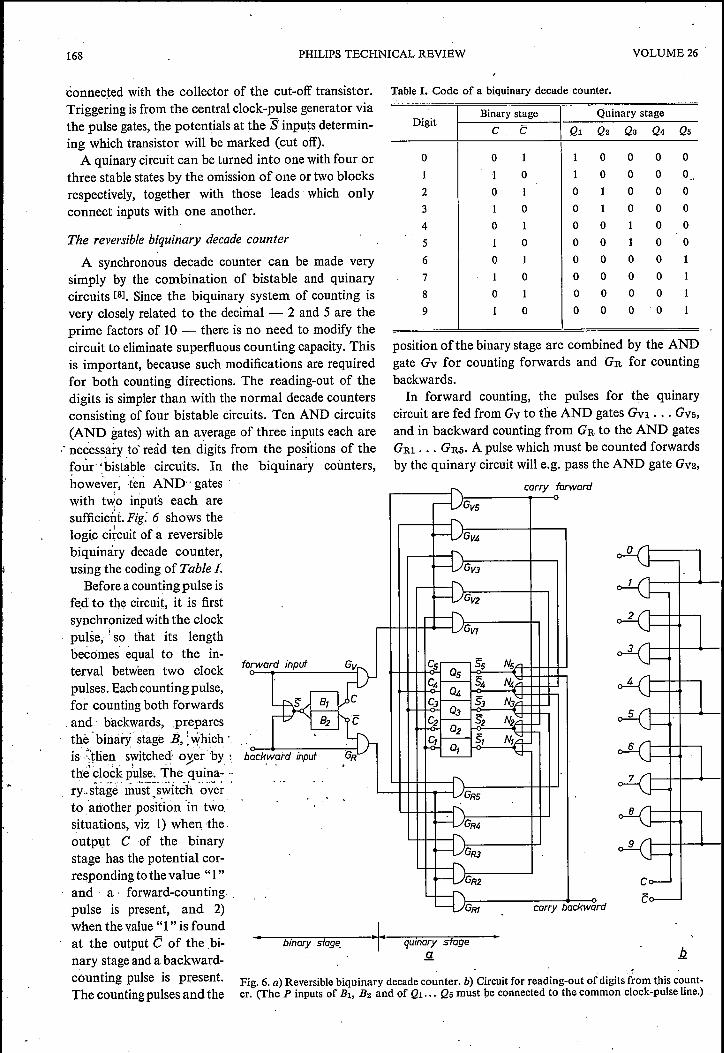
The reversible biquinary decade counter
A synchronous decade counter can be made verysimply by the combination of bistable and quinarycircuits [8J. Since the biquinary system of counting isvery closely related to the decimal - 2 and 5 are theprime factors of 10 - there is no need to modify thecircuit to eliminate superfluous counting capacity. Thisis important, because such modifications are requiredfor both counting directions. The reading-out of thedigits is simpler than with the normal decade countersconsisting of four bistable circuits. Ten AND circuits(AND gates) with an average of three inputs each are
: necessary to' read .ten digits from the positions of thefour 'bist~ble circuits. In the biquinary counters,however, ·fen AND' gateswith two inputs each aresufficie~t. Fig: 6 shows thelogic ci~cuitof a reversiblebiquinary decade counter,using the coding of Table J.
Before a counting pulse isfed to. the circuit, it is firstsynchronized with the clockpulse, . so that its length. becomes equal to the in-terval between two clockpulses. Eachcounting pulse,for counting both forwardsand backwards, preparesthè .binary stage B,:Which'is ttlien switched over by t
.,', i· ~ .' /'
the clock-pulse. The quina- ..rye. s'i:äg~.mûst-switch 'övei-"to another po;iÜon in two.situations, viz 1) when the.output C of the binarystage has the potential cor-responding to the value "1"and a forward-countingpulse is present, and 2)when the value "1" is foundat the output C of the .bi-nary stage and a backward-counting pulse is present.The counting pulses and the
connected with the collector of the cut-off transistor. Table I. Code of a biquinary decade counter.
Triggering is from the central clock-pulse generator viathe pulse gates, the potentials at the S inputs determin-ing which transistor will be marked (cut off).
A quinary circuit can be turned into one with four orthree stable states by the omission of one or two blocksrespectively, together with those leads which onlyconnect inputs with one another.
DigitBinary stage
IQuinary stage
C C Ql Q2 Qa Q4 Qs
0 0 1 1 0 0 0 0
1 1 0 1 0 0 0 0 ..2 0 1 0 1 0 0 0
3 1 0 0 1 0 0 0
4 0 1 0 0 1 0 0
5 1 0 0 0 1 0 0
6 0 1 0 0 0 0 1
7 1 0 0 0 0 0 1
8 0 1 0 0 0 0 1
9 1 0 0 0 0 0 1
position ofthe binary stage are combined by the ANDgate Gv for counting forwards and GR for countingbackwards.In forward counting, the pulses for the quinary
circuit are fed from Gv to the AND gates GVI ... GV5,and in backward counting from GR to the AND gatesGRI ... GR5. A pulse which must be counted forwardsby the quinary circuit will e.g. pass the AND gate GV2,
carry forwardl7---'--_"'--oGV5
ë
GVI
carry backward
-I-binary stage. qwnary stages:
Fig. 6. a) Reversible biquinary decade counter. b) Circuit for reading-out of digits from this count-er. (The P inputs of Bi, B2 and of Ql .•• Q5 must be connected to the common clock-pulse line.)

1965, No. 4/5/6 SYSTEM OF DIGITAL CIRCUIT BLOCKS 169
which is opened by the "1" signal at the output C2 ofstage Q2, thus priming the signal input S3 of the nextstage (in the forward direction) Q3. Similarly, witha pulse that has to be counted backwards the ANDgate GR2 is opened and the next stage (in the reversedirection) Ql is primed via the signal input. The actualswitching-over is always initiated by the next clockpulse to coincide with the counting pulse.
Special circuits
A multivibrator can be built up of two active blocksby connecting their outputs C crosswise via capaci-tors Cz to the direct base leads Bo and by connectingboth the leads which are normally intended for thenegative and the positive supply voltages to the positivesupply voltage.
In the monostabie circuit the static coupling - as inthe bistable - is formed by the combination RIC, CI<,D4 and D5. An external capacitor Cz, which must beconnected between the collector C and the base in-put Be; determines the delay time. The base bias resist-ance of the capacitively coupled transistor is connectedto the positive supply voltage, so that this transistorconducts in the stationary state. The monostabIe circuitis triggered via the P input of the capacitively coupledblock.
A Schmitt trigger is formed by connecting two activeblocks in series, the emitter leads 0 being earthed via acommon resistor. The threshold level can be adjustedby means of another external resistor connecting thedirect base lead Bo of the first block with the positivesupply voltage. Excitation is via one of the NOR inputsof the first stage.
Loading rules
The combination of active and passive blocks to givea logic circuit must be done in accordance with theloading rules, since each block is loaded by the sub-sequent stages and itself forms a load for the previousstage. Because there are only two types of circuit block,the loading rules can be kept simple.
Each input Bi ... Bn of an active block (NOR)represents a "NOR load" for the previous stage. Eachinput El ... Em of a passive block (AND gate) repre-sents a certain number of "gate loads" for the previousNOR stage; this number depends on the choice of thetotal gate resistance:
13Re/21 Rc Re/2 Re/3---------------------- I 2/3 I 2 3
Total gate resistance
Number of gate loads k
These two types of load may not be discounted againstone another when calculating the maximum permissible
load.
With a few exceptions, which cannot be discussedwithin the scope of this article, the following simplifiedloading table is obtained (where allowance must still bemade for the restrietion mentioned on page 167 for theNOR circuit for signal inversion at the S input of abistable circuit):
Previous stage Type of load Load
NOR AND g ~ 8; 'i:.k ~ 8
NOR NOR 11~4
AND NOR lI~k
Here g is the maximum number of gate loads whichcan be carried by a NOR stage (gate loads must beadded, no matter whether the AND gates are connectedin parallel or in series), k is the number of gate loadscorresponding to an AND gate, and n the maximumnumber of NOR loads that can be carried by theprevious stage.
Fig. 7 shows a possible realization of a NOR block
"It' \\
I.;Fig. 7. Examples of the construction of two circuit blocks, as usede.g. in electronic weighing installations. Above AND circuit,centre and below: NOR circuit.
[8] F. Bregman, Counting circuits equipped with transistors,Philips Research Laboratories Eindhoven, unpublished work.E. Schurig, "UZ 71" - Ein neuer Universalzähler, Elektron.Rdsch. 16,111-114,1962.R. A. Hernpel, A 100 kc add-subtract transistorized decadecounter, Semiconductor Prod. 5, 19-24, 1962.

170 PHILlPS TECHNICAL REVIEW VOLUME 26
Generation of musical intervals by a digital method
and of an AND block. In order to increase the economyof this system, these two types of block can be sup-plemented by another active block consisting of twoNOR circuits without pulse gate. These can be used
Fig. 8. Construction ofa synchronous reversible biquinary decadecounter with output amplifiers.
Introduetion
The familiar kinds of musical instrument can bedivided into two classes:a) Instruments producing notes whose pitch is not
decided upon until the instant of playing: bowedstring instruments and certain wind instrumentsare examples.
b) Instruments possessing a store of notes, from whichin the course of playing a selection is made inaccordance with a programme. All keyboard in-struments belong to this class.
Instruments in class (b) can only be endowed with alimited store of notes for constructional reasons, andbecause the technique of execution might otherwise berendered too difficult; also, the access time for what-ever notes are available must be compatible with prae-
Dipl.-II/g. D. Gosset is a research worker at the Hamburg labora-tory of Philips Zentra/laboratorium GmbH,
with advantage wherever the NOR does not form partof a bistable or polystable circuit.
Fig.8 shows a reversible biquinary decade counterwith 10 output amplifiers for the digits o ... 9.
The system of circuit blocks described here has beenused in electronic weighing installations with digitaldata encoding and processing.
The synchronous biquinary decade counter wasdeveloped by P. Muuss of the Hamburg Laboratory.
Summary. This paper describes a new system of digital circuitblocks, designed to meet the special needs of industrial measure.ment and control techniques, characterized by the following.a) It contains only two different basic circuits: an active logic
circuit in diode-transistor logic (DTL), and a passive logiccircuit in diode logic.
b) It contains only one type of transistor and two types of diode;there are no emitter-followers.
c) The basic circuits of this system can be combined to give notonly bistable but also polystable circuits with for example3, 4 or 5 stable states.
d) The bistable circuits can be used for either the synchronousor the asynchronous counting mode.
e) The circuit blocks operate reliably under full load in thetemperature range from -10°C to +50 °C with the mostunfavourable values of the resistances and voltages withintheir tolerances, and with the smallest current amplificationand the greatest leakage currents which can occur at the endof life of the transistor.
f) The loading table is simple.g) Special circuits, such as multivibrators, monostabIe circuits
as well as Schmitt triggers, can be realized by simple combi.nation of two active blocks and one or two extra resistors orcapacitors.
D. Gossel 534.321.2 :621.389
tical requirements for playing the instrument. This im-plies the existence of some fixed rule or instruction forselecting individual tones from the continuum of pitch.
Several such rules have been laid down at varioustimes in the history of music [1], they find practicalexpression in the various tonal or tuning systems. Thefour most important will now be briefly explained anddiscussed.
Tonal systems
A tonal system has been defined [2] as a scheme fordividing the octave into a progressive sequence of tones,the principle underlying the division being consistentlyadhered to and designed to produce musically accept-able intervals.
1. Pythagorean tuning
This system dates back to the philosopher who livedduring the 6th century BC. It is based upon the fifth,