A Customer Programmable Microfluidic System
154
University of Central Florida University of Central Florida STARS STARS Electronic Theses and Dissertations, 2004-2019 2008 A Customer Programmable Microfluidic System A Customer Programmable Microfluidic System Miao Liu University of Central Florida Part of the Mechanical Engineering Commons Find similar works at: https://stars.library.ucf.edu/etd University of Central Florida Libraries http://library.ucf.edu This Doctoral Dissertation (Open Access) is brought to you for free and open access by STARS. It has been accepted for inclusion in Electronic Theses and Dissertations, 2004-2019 by an authorized administrator of STARS. For more information, please contact [email protected]. STARS Citation STARS Citation Liu, Miao, "A Customer Programmable Microfluidic System" (2008). Electronic Theses and Dissertations, 2004-2019. 3702. https://stars.library.ucf.edu/etd/3702
Transcript of A Customer Programmable Microfluidic System
University of Central Florida University of Central Florida
STARS STARS
Electronic Theses and Dissertations, 2004-2019
2008
A Customer Programmable Microfluidic System A Customer Programmable Microfluidic System
Miao Liu University of Central Florida
Part of the Mechanical Engineering Commons
Find similar works at: https://stars.library.ucf.edu/etd
University of Central Florida Libraries http://library.ucf.edu
This Doctoral Dissertation (Open Access) is brought to you for free and open access by STARS. It has been accepted
for inclusion in Electronic Theses and Dissertations, 2004-2019 by an authorized administrator of STARS. For more
information, please contact [email protected].
STARS Citation STARS Citation Liu, Miao, "A Customer Programmable Microfluidic System" (2008). Electronic Theses and Dissertations, 2004-2019. 3702. https://stars.library.ucf.edu/etd/3702
A CUSTOMER PROGRAMMABLE MICROFLUIDIC SYSTEM
by
MIAO LIU
B.S. Tsinghua University, 2000
M.S. Tsinghua University, 2002
A dissertation submitted in partial fulfillment of the requirements
for the degree of Doctor Philosophy
in the Department of Mechanical, Materials, and Aerospace Engineering
in the College of Engineering and Computer Science
at the University of Central Florida
Orlando, Florida
Fall Term
2008
Major Professor: Quanfang Chen

© 2008 Miao Liu
ii
ABSTRACT
Microfluidics is both a science and a technology offering great and
perhaps even revolutionary capabilities to impact the society in the future.
However, due to the scaling effects there are unknown phenomena and technology
barriers about fluidics in microchannel, material properties in microscale and
interactions with fluids are still missing. A systematic investigation has been
performed aiming to develop “A Customer Programmable Microfluidic System”.
This innovative Polydimethylsiloxane (PDMS)-based microfluidic system
provides a bio-compatible platform for bio-analysis systems such as Lab-on-a-
chip, micro-total-analysis system and biosensors as well as the applications such
as micromirrors. The system consists of an array of microfluidic devices and each
device containing a multilayer microvalve. The microvalve uses a thermal
pneumatic actuation method to switch and/or control the fluid flow in the
integrated microchannels. It provides a means to isolate samples of interest and
channel them from one location of the system to another based on needs of
realizing the customers’ desired functions.
Along with the fluid flow control properties, the system was developed
and tested as an array of micromirrors. An aluminum layer is embedded into the
PDMS membrane. The metal was patterned as a network to increase the
reflectivity of the membrane, which inherits the deformation of the membrane as a
mirror. The deformable mirror is a key element in the adaptive optics. The
proposed system utilizes the extraordinary flexibility of PDMS and the
iii
addressable control to manipulate the phase of a propagating optical wave front,
which in turn can increase the performance of the adaptive optics.
Polydimethylsiloxane (PDMS) has been widely used in microfabrication
for microfluidic systems. However, few attentions were paid in the past to
mechanical properties of PDMS. Importantly there is no report on influences of
microfabrication processes which normally involve chemical reactors and
biologically reaction processes. A comprehensive study was made in this work to
study fundamental issues such as scaling law effects on PDMS properties,
chemical emersion and temperature effects on mechanical properties of PDMS,
PDMS compositions and resultant properties, as well as bonding strength, etc.
Results achieved from this work will provide foundation of future developments
of microfluidics utilizing PDMS.

iv
This dissertation is dedicated to my parents, Weiping Liu and Yuqi Zhu, for
always loving me, believing in me, inspiring me and encouraging me to be a
strong woman in the engineering field and reach higher to achieve my dream.
v
ACKNOWLEDGMENTS
I would like to express my sincere gratitude and thanks to my advisor, Dr.
Quanfang Chen, for his academic guidance, understanding, patience, and financial
support during my PhD study at University of Central Florida. I would also like to
thank my committee members, Dr. David W. Nicholson, Dr. Jayanta Kapat, Dr.
Ming Su and Dr. Kiminobu Sugaya for their suggestions and encouragements
during the preparation of this dissertation.
Carrying out this research would not have been possible without the help
of all the members of MEMS lab. Thank you for your assistance and meaningful
contribution to this work.
A sincere appreciation goes to Dr. Weixing Xu and Dr. Bo Li. Thanks for
being my best friends and giving me the support and help I needed during this
long journey. Special thanks go to Mr. Christopher Bock for the help of editing
and proof reading this dissertation.
I thank my parents for supporting me through these many years of study.
They have always believed in me, unconditionally loved me and encouraged me
to try my best in every step of my life. To them, I am forever grateful.
Last but not least, I would like to thank my fiancé, Lin Wang, for his
encouragement, support, trust and love. He gave me the final courage and strength
to cross the finish line and the confidence to be myself again.
vi
TABLE OF CONTENTS
LIST OF FIGURES ................................................................................................ ix
LIST OF TABLES ................................................................................................. xv
CHAPTER 1 INTRODUCTION ............................................................................. 1
1.1 Background for the Study .............................................................................. 1
1.2 Microfluidic System....................................................................................... 8
1.2.1 Recent Development of Microfluidic System......................................... 8
1.2.2 Components of Microfluidic System .................................................... 10
1.4 PDMS and Soft Lithography ....................................................................... 35
1.3.1 Introduction of PDMS .......................................................................... 36
1.3.2 Soft Lithography ................................................................................... 39
CHAPTER 2 PROGRAMMABLE MICROFLUIDIC SYSTEM ......................... 46
2.1 Introduction .................................................................................................. 46
2.2 Design and Simulation ................................................................................. 47
2.2.1 Design ................................................................................................... 48
2.2.2 Basic Theory ......................................................................................... 50
2.3 Fabrication ................................................................................................... 58
2.3.1 Fabrication of Microheater and Microchamber .................................... 58
2.3.2 Fabrication of Microchannel ................................................................. 60
2.3.3 Bonding between Microchamber and Microchannel ............................ 61
vii
2.4 Test Result and Discussion .......................................................................... 62
2.4.1 Test Method Setup ................................................................................ 62
2.4.2 Test Results and Discussion.................................................................. 63
2.5 Conclusion and Outlook .............................................................................. 67
4.1 Introduction .................................................................................................. 69
4.2 Design and Simulation ................................................................................. 70
4.3 Fabrication ................................................................................................... 72
4.4 Test Results and Discussion......................................................................... 76
4.5 Conclusion and Outlook .............................................................................. 79
CHAPTER 3 MECHANICAL PROPERTIES OF PDMS .................................... 81
3.1 Introduction .................................................................................................. 81
3.2 Standards for Mechanical Properties Tests .................................................. 84
3.2.1 Tensile Test ........................................................................................... 85
3.2.2 Bending Test ......................................................................................... 87
3.2.3 Resonant Test ........................................................................................ 88
3.2.4 Membrane Test ..................................................................................... 89
3.3 Methodology ................................................................................................ 90
3.3.1 Experiment Method .............................................................................. 91
3.3.2 Specimen Design .................................................................................. 91
3.3.3 Specimen Fabrication............................................................................ 93
viii
3.3.4 Testing Setup ........................................................................................ 98
3.4 Results and Discussion ................................................................................ 99
3.4.1 Mechanical Properties of PDMS with Different Mixing Ratios ........... 99
3.4.2 Size Effect on Mechanical Properties of PDMS ................................. 103
3.4.3 Chemical Immersion Effects on Mechanical Properties of PDMS .... 106
3.4.4 Temperature Effects on Mechanical Properties of PDMS .................. 120
3.5 Conclusion ................................................................................................. 122
CHAPTER 4 CONCLUSION AND OUTLOOK................................................ 124
REFERENCES .................................................................................................... 128
ix
LIST OF FIGURES
Figure 1 Biosite Triage System................................................................................ 6
Figure 2 Market for Microfluidic Technologies, 1997-2008 ($ Millions)............... 9
Figure 3 Micropumps categories by their pumping principles .............................. 11
Figure 4 Review of micropump technologies Green represents mechanical
micropumps, and pink non-mechanical ................................................................. 12
Figure 5 Schematic of the first reciprocating displacement micropump ............... 14
Figure 6 Schematic of the first thermopneumatic micropump ............................. 15
Figure 7 Photo of the planar micropump utilizing two platinum hearers for
thermopneumatic actuation and two in-plane flaps valves .................................... 16
Figure 8 Cross-sectional view of the valve seat showing that all leakage paths
around the valve seat are sealed ............................................................................. 16
Figure 9 Schematic view of an electrostatically driven diaphragm ....................... 17
Figure 10 Induction EHD pumps ........................................................................... 21
Figure 11 Electroosmotic flow in a channel .......................................................... 22
Figure 12 Electric double layer .............................................................................. 23
Figure 13 Schematic diagram of the actuation principle of the MHD micropump
where driving force is Lorentz force ...................................................................... 24
Figure 14 Elements of a simple adaptive optical imaging system ......................... 28
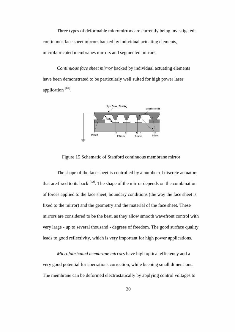
Figure 15 Schematic of Stanford continuous membrane mirror ............................ 30
Figure 16 Principle of operation of deformable viscoelastic mirror ...................... 32
x
Figure 17 Schematic of micromirror with a continuous membrane ...................... 33
Figure 18 Electroactive polymer deformable micromirror .................................... 34
Figure 19 Principle of the magnetic mirror ............................................................ 34
Figure 14 Chemical formulas of PDMS ................................................................ 36
Figure 15 PDMS in soft lithography ...................................................................... 40
Figure 16 Microcontact printing ............................................................................ 41
Figure 17 Microtransfer molding ........................................................................... 41
Figure 18 Micromolding in capillaries .................................................................. 42
Figure 19 Replica molding..................................................................................... 43
Figure 20 Solvent-assisted micromoldings ............................................................ 43
Figure 21 Phase-shift photolithography ................................................................. 44
Figure 22 Single unit device in proposed system .................................................. 48
Figure 23 Design concept ...................................................................................... 49
Figure 24 Integration of array and control bus ...................................................... 50
Figure 25 Semi-sphere bubble diagram ................................................................. 51
Figure 26 Bubble radius and pressure vs. time with 108 W/m
2 heat flux .............. 52
Figure 27 Temperatures and pressures of Vapor in Bubbles ................................. 54
Figure 28 Simplified Model of Parallel Metallic Electrodes ................................. 55
Figure 29 Fabrication process of microheater and microchamber......................... 59
Figure 30 Deformation and fabrication of spiral shape electrode .......................... 60
xi
Figure 31 Fabrication of microchannel .................................................................. 60
Figure 32 Monitoring system setup ....................................................................... 62
Figure 33 Measuring system setup ........................................................................ 63
Figure 34 Microheater and microchamber ............................................................. 63
Figure 35 Testing result of deformed membrane under 5V actuation ................... 64
Figure 36 Comparison of experimental and simulated deformation of PDMS
membrane ............................................................................................................... 64
Figure 37 Spiral shape photoresist pattern ............................................................. 65
Figure 38 SEM of O2 plasma etched PDMS surfaces............................................ 66
Figure 39 PDMS microchannel fabricated using re-flow method ......................... 66
Figure 40 Bonding effect between PDMS parts with different mixing ratios ....... 67
Figure 47 Micromirror array design ( single array) ............................................... 71
Figure 48 Simulation of micromirror array ........................................................... 72
Figure 49 Evaporated gold layer on PDMS substrate ............................................ 73
Figure 50 Fabrication of Aluminum Micromirrors Arrays .................................... 74
Figure 51 Aluminum micromirror array on PDMS substrate ................................ 75
Figure 52 Veeco measurement of surface condition of aluminum micromirror on
PDMS substrate ..................................................................................................... 76
Figure 53 Test Chamber for micromirror arrays.................................................... 77
Figure 54 Aluminum Micromirror arrays on PDMS substrate .............................. 77
xii
Figure 55 Veeco measurement of deformed micromirror array ............................ 78
Figure 56 Comparison of simulated and actual deformed mirror array ................. 79
Figure 57 Tensile test configurations ..................................................................... 86
Figure 58 Micro cantilever bending ....................................................................... 87
Figure 59 MTS Tytron 250 Micro Force Tester with PDMS samples mounted on
through two leveled clamps and control software interface .................................. 90
Figure 60 Specimen design geometry .................................................................... 92
Figure 61 Molding method for specimen preparation ........................................... 94
Figure 62 Specimen prepared with molding method ............................................. 95
Figure 63 Hot embossing method for specimen preparation ................................. 95
Figure 64 Electroplating experiment setup ............................................................ 96
Figure 65 SU-8 mold on Cr/Cu coated wafer (left) and electroplated Cu after
release (right) ......................................................................................................... 96
Figure 66 Fabrication process of samples for chemical immersion test ................ 98
Figure 67 Customerized gripper ............................................................................ 98
Figure 68 Tensile test procedure ............................................................................ 99
Figure 69 Stress-strain relationship of PDMS with mixing ratio 10:1 ................ 100
Figure 70 Young’s modulus versus weight mixing ratio ..................................... 101
Figure 71 bonded PDMS with the same orientation of bonding surface ............. 101
Figure 72 Bonding strength strongly depends on the mixing ratio ...................... 102
xiii
Figure 73 Ultimate tensile stress vs. length and thickness................................... 104
Figure 74 Young’s modulus vs thickness ............................................................ 105
Figure 75 Strain-stress Curve of PDMS after Acetone Immersion ..................... 106
Figure 76 Young’s modulus of PDMS after immersion in Acetone and
Isopropanol .......................................................................................................... 107
Figure 77 Young’s Modulus of PDMS after Immersion in Methanol and Ethanol
.............................................................................................................................. 108
Figure 78 Ultimate Tensile Stresses of PDMS after Immersion in Acetone,
Isopropanol, Methanol and Ethanol ..................................................................... 109
Figure 79 Elongations of PDMS after Immersion in Acetone, Isopropanol,
Methanol and Ethanol .......................................................................................... 110
Figure 80 Young's modulus, UTS and elongation of PDMS after SU-8 developer
immersion ............................................................................................................ 112
Figure 81 Young's modulus of PDMS after nitric acid immersion ..................... 113
Figure 82 Ultimate tensile stress of PDMS after nitric acid immersion .............. 113
Figure 83 Elongation of PDMS after nitric acid immersion ................................ 114
Figure 84 Young’s Modulus of PDMS after Ni Electroplating Solution
Immersion at 45°C and 60°C ............................................................................... 116
Figure 85 Ultimate Tensile Stress of PDMS after Ni Electroplating Solution
Immersion at 45°C and 60°C ............................................................................... 116
Figure 86 Young’s Modulus of PDMS after Cu Electroplating Solution Immersion
.............................................................................................................................. 117
Figure 87 UTS of PDMS after Cu Electroplating Solution Immersion ............... 118

xiv
Figure 88 Young's modulus of PDMS with PCR immersion .............................. 119
Figure 89 Young’s modulus of PDMS with temperature effect .......................... 121
Figure 90 Ultimate tensile stress of PDMS with temperature effect ................... 121
xv
LIST OF TABLES
Table 1 Potential applications of microfluidic systems ........................................... 2
Table 2 Comparison of different actuation methods.............................................. 12
Table 3 Cured RTV 615 properties ........................................................................ 37
Table 4 Properties of water vapor .......................................................................... 52
Table 5 Bonding ratio pair ..................................................................................... 92
Table 6 Nickel electroplating solution recipe ...................................................... 115
Table 7 Copper electroplating solution recipe ..................................................... 117
Table 8 Tensile test results of PDMS after 30 cycles PCR test ........................... 119

1
CHAPTER 1 INTRODUCTION
1.1 Background for the Study
Since the first research in microfluidics was carried out in 1977[1]
, the
research in this area has undergone an enormous growth and many different
microfluidic devices have been developed. Microfluidic devices assure the
manipulation of liquids and gases in channels having cross-sectional dimensions
on the order of 10 ~100 μm. Microfluidic systems comprising of micronozzles,
microchannels, micropumps, micromixers, and microvalves, etc., can be used for
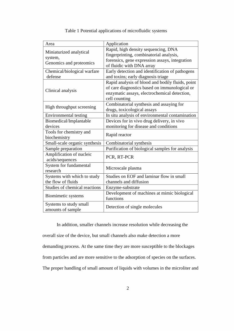
a variety of applications (Table 1) involving general manipulation of liquid, gases
and their mixtures. As such, microfluidics is an important technology in a number
of miniaturized systems that are being developed for chemical, biological and
medical applications, and even systems for fundamental research.
Compared to conventional macro-scale fluidic systems, microfluidic
devices and systems have a number of significant advantages such as: enhanced
performances in reaction/detection, low cost, compact size, disposability, smaller
volumes of reagents or samples and low energy consumption. For example,
microfluidic channels can approximate the size and flow condition found in in-
vivo capillaries around 10 μm with 0.1 cm/s. The use of research and diagnostic
devices of with similar sizes and elasticity as those found in biology could lead to
more accurate information and greater understanding of physiology.
2
Table 1 Potential applications of microfluidic systems
Area Application
Miniaturized analytical
system,
Genomics and proteomics
Rapid, high density sequencing, DNA
fingerprinting, combinatorial analysis,
forensics, gene expression assays, integration
of fluidic with DNA array
Chemical/biological warfare
defense
Early detection and identification of pathogens
and toxins; early diagnosis triage
Clinical analysis
Rapid analysis of blood and bodily fluids, point
of care diagnostics based on immunological or
enzymatic assays, electrochemical detection,
cell counting
High throughput screening Combinatorial synthesis and assaying for
drugs, toxicological assays
Environmental testing In situ analysis of environmental contamination
Biomedical/Implantable
devices
Devices for in vivo drug delivery, in vivo
monitoring for disease and conditions
Tools for chemistry and
biochemistry Rapid reactor
Small-scale organic synthesis Combinatorial synthesis
Sample preparation Purification of biological samples for analysis
Amplification of nucleic
acids/sequences PCR, RT-PCR
System for fundamental
research Microscale plasma
Systems with which to study
the flow of fluids
Studies on EOF and laminar flow in small
channels and diffusion
Studies of chemical reactions Enzyme-substrate
Biomimetic systems Development of machines at mimic biological
functions
Systems to study small
amounts of sample Detection of single molecules
In addition, smaller channels increase resolution while decreasing the
overall size of the device, but small channels also make detection a more
demanding process. At the same time they are more susceptible to the blockages
from particles and are more sensitive to the adsorption of species on the surfaces.
The proper handling of small amount of liquids with volumes in the microliter and
3
the nanoliter range has become extremely important with the development of
μTAS (micro-total-analysis-system) and Lab-on-chip. These technologies have
been applied in a variety of areas including separation science, chemical synthesis
and immunoassays, DNA amplification and sequencing, protein separations and
single-cell analysis. Microfluidic systems have been developed to conduct a wide
range of DNA analyses. Polymerase chain reactions (PCR) have been successfully
carried out within integrated microfluidic systems. DNA sequencing and
genotyping are achieved using microchannels and capillary array electrophoresis.
Microfluidics technology has also illustrated a potential to be allied with the
detection of very low numbers of DNA molecules. Single molecule detection has
been achieved in a Polydimethylsiloxane (PDMS) channel using near field
optics[2]
.
Miniaturized microfluidic systems require the ability to control precisely
and efficiently the transport of reagents and samples throughout the different parts
of the system. Most of these systems are developed with bulk and surface
micromachining processes using microfabrication techniques on silicon, glass or
polymer substrates.
A great variety of microchip fabrications and materials are used for
producing highly sophisticated two- and three-dimensional microstructures with
integrated modules. The earliest microfluidic systems were fabricated in silicon
and glass to take advantages of the technology already existing in
microelectronics and microelectromechanical system (MEMS). Although Silicon
4
and glass are attractive materials for fabricating microfluidic devices, polymers
also have unique characteristics. Polymers are less expensive than silicon and
glass and involve simpler and less expensive manufacturing processes. Lower
production costs also mean that single-use devices, which eliminate contamination
between analyses, are more feasible in applications. Examples of polymers used to
fabricate microfluidic systems include: polyurethane [3]
, polycarbonate [4, 5]
,
polymethylmethacrylate (PMMA) [6-8]
, polystyrene[9]
, polyethyleneterephthalate
glycol (PETG) [10]
, polyethylene [11]
and Polydimethylsiloxane (PDMS) [12-15]
.
Soft polymers (elastomers) have additional advantages for microfluidic
device fabrication. Particularly, PDMS is a soft polymer that is being actively
used in both academic and industrial research groups for applications in
microfluidics. PDMS devices are fabricated by soft lithography, a technique that
allows rapid prototyping of microfluidic devices. Soft lithography is particularly
useful as a non-photolithographic technique for pattern replication to enable rapid
prototyping of devices. Devices made of PDMS can be easily integrated with
outside components because the polymer conforms to most materials and both
reversible and irreversible sealing are possible. This polymer is attractive for
applications requiring temperature gradients since it is stable at temperatures
necessary for processing biological substrates. PDMS is also bio-compatible with
many optical detection methods because it is transparent in the visible/UV region.
PDMS channels are appropriate for cellular studies because PDMS is nontoxic to
proteins and cells. These good characteristics have made it the key material for
exploratory research and research engineering at the early stages in the
5
development of microfluidic systems. Two particularly important achievements
have been the development of soft lithography in PDMS as a method for
fabricating prototype devices and the development of a simple method of
fabricating pneumatically activated valves, mixers and pumps on the basis of soft-
lithographic procedures. These methods have made it possible to fabricate devices
that test new ideas with a faster pace using silicon technology. Quake’s pneumatic
valves[16]
are particularly important as components that have enabled the design
and examination of complicated devices and these have opened up a number of
areas of applications. “Quake valves” use the restriction of a fluidic channel by an
adjacent channel under pressure; their operation depends on the fact that PDMS is
an elastomer and no corresponding devices exist in rigid materials such as silicon
and glass. And also, microfluidic systems are studied by Janasek et al to exploit
the scaling law that relate macroscopic and microfluidic systems with special
emphasis on lab-on-a-chip devices[17]
.
While microelectronics emphasis component size reduction, microfluidics
research is focused on making more complex system with better fluid-handling
capabilities using macro system components such as pumps valves mixers, filters
and separators at microscale. With this possibility of integration, the ultimate goal
for microfluidic system is to be able to detect biological molecules, transport, mix
and characterize a raw sample, all with one device. The domain of this kind of
integrated analysis systems has been designated as μTAS or also lab-on-chip
systems. In 1994, S. Jacobson [18]
first fabricated a chip integrating three different
functions: mixing, reaction and separation. This achievement was just the
6
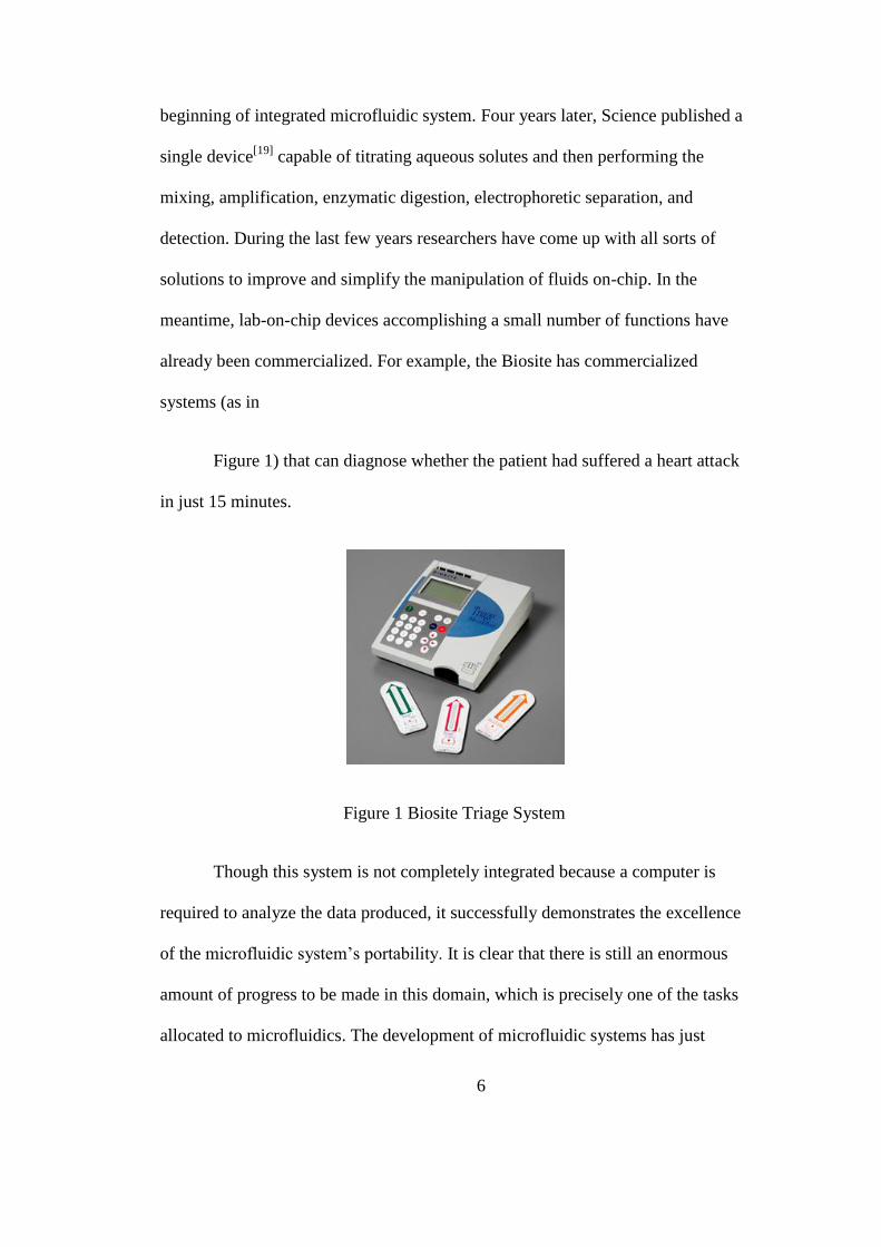
beginning of integrated microfluidic system. Four years later, Science published a
single device[19]
capable of titrating aqueous solutes and then performing the
mixing, amplification, enzymatic digestion, electrophoretic separation, and
detection. During the last few years researchers have come up with all sorts of
solutions to improve and simplify the manipulation of fluids on-chip. In the
meantime, lab-on-chip devices accomplishing a small number of functions have
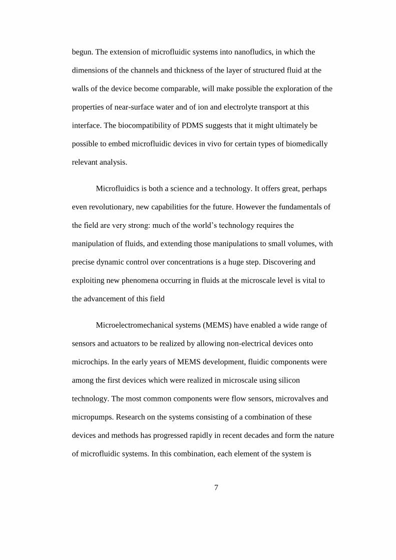
already been commercialized. For example, the Biosite has commercialized
systems (as in
Figure 1) that can diagnose whether the patient had suffered a heart attack
in just 15 minutes.
Figure 1 Biosite Triage System
Though this system is not completely integrated because a computer is
required to analyze the data produced, it successfully demonstrates the excellence
of the microfluidic system’s portability. It is clear that there is still an enormous
amount of progress to be made in this domain, which is precisely one of the tasks
allocated to microfluidics. The development of microfluidic systems has just
7
begun. The extension of microfluidic systems into nanofludics, in which the
dimensions of the channels and thickness of the layer of structured fluid at the
walls of the device become comparable, will make possible the exploration of the
properties of near-surface water and of ion and electrolyte transport at this
interface. The biocompatibility of PDMS suggests that it might ultimately be
possible to embed microfluidic devices in vivo for certain types of biomedically
relevant analysis.
Microfluidics is both a science and a technology. It offers great, perhaps
even revolutionary, new capabilities for the future. However the fundamentals of
the field are very strong: much of the world’s technology requires the
manipulation of fluids, and extending those manipulations to small volumes, with
precise dynamic control over concentrations is a huge step. Discovering and
exploiting new phenomena occurring in fluids at the microscale level is vital to
the advancement of this field
Microelectromechanical systems (MEMS) have enabled a wide range of
sensors and actuators to be realized by allowing non-electrical devices onto
microchips. In the early years of MEMS development, fluidic components were
among the first devices which were realized in microscale using silicon
technology. The most common components were flow sensors, microvalves and
micropumps. Research on the systems consisting of a combination of these
devices and methods has progressed rapidly in recent decades and form the nature
of microfluidic systems. In this combination, each element of the system is
8
miniaturized by micromachining and is integrated on a substrate. This process
reduces the system size, cost, and dead volume. The sample volumes and the
amount of reagents needed for measurements are also significantly reduced so that
the measurement time may be reduced and the power consumption for the entire
system can be decreased. With the growing importance of genomics, proteomics,
and the discovery of new drugs, microfluidics expanded to the development of
numerous micro devices: filters, mixers, reactors, separators. New effects such as
electro-kinetic effects, acoustic streaming, magnetohydrodynamic effects,
electrochemical, and more, which were previously neglected in macroscopic
applications, have now gained new importance in microscale systems.
1.2 Microfluidic System
1.2.1 Recent Development of Microfluidic System
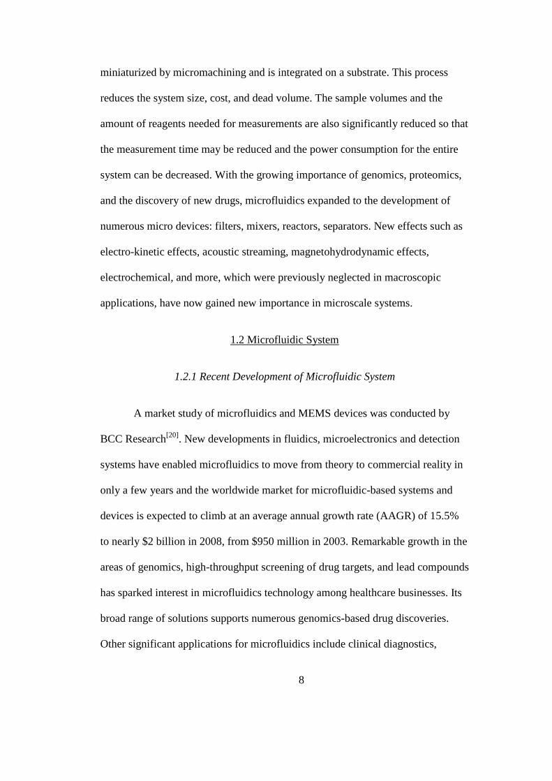
A market study of microfluidics and MEMS devices was conducted by
BCC Research[20]
. New developments in fluidics, microelectronics and detection
systems have enabled microfluidics to move from theory to commercial reality in
only a few years and the worldwide market for microfluidic-based systems and
devices is expected to climb at an average annual growth rate (AAGR) of 15.5%
to nearly $2 billion in 2008, from $950 million in 2003. Remarkable growth in the
areas of genomics, high-throughput screening of drug targets, and lead compounds
has sparked interest in microfluidics technology among healthcare businesses. Its
broad range of solutions supports numerous genomics-based drug discoveries.
Other significant applications for microfluidics include clinical diagnostics,
9
proteomics, glycomics, cell manipulation, tissue engineering, structural biology,
combinatorial chemistry, environmental monitoring, and drug delivery. The
popularity of miniaturization is expected to fuel the market. The extraordinary
ability to also shrink sample volumes down to the microscale is expected to make
microfluidic systems attractive to the biomedical industry.
Figure 2 Market for Microfluidic Technologies, 1997-2008 ($ Millions)
Microfluidic systems have the tremendous potential both in fundamental
research fields and everyday applications such as inkjet printers, blood-cell-
separation equipment, biochemical assays, chemical synthesis, genetic analysis
and drug screening. With the development in fabrication and MEMS materials,
microfluidic systems are now rapidly evolving towards their ultimate goal: fast,
portable, robust, flexible, inexpensive and easy-to-use all-add-on systems which is
one system to provide all of the possible required analyses for a given type
problem. And this leads to the concept of “lab-on-chip” or μTAS. Synthesis,
purification, analysis and diagnostics would be performed by such a system
rapidly, economically and with minute volumes of samples. The microfluidic
systems on the“chip” perform as small platforms comprising channel systems
10
connected to liquid reservoirs by tubing systems in turn linked to syringes. The
channel measures in the range of a few micrometers, which greatly facilitates the
handling of volumes much smaller than a microliter. Appropriate channel design
and integrated modules such as electrodes or a specific pattern are now facilitating
the incorporation of many operational steps. As microfluidic systems continue to
evolve, it will be very important to have portable application codes that can run
without modification on successive generations of chips. Since the first μTAS, the
micro gas chromatograph (GC) created by a group from Stanford University in the
late 1970s, the development of μTAS lead researchers to the realization of a
number of successive operations such as blood gas analysis, glucose/lactate
analysis, DNA analysis, proteomics analysis, combinatorial synthesis analysis,
immunoassays, toxicity monitoring and even forensic analysis applications.
1.2.2 Components of Microfluidic System
A microfluidic system must have a series of generic components: a method
of introducing reagents and samples (probably as fluids or gas or even particles),
methods for moving these fluids around on the chip and for combining and mixing
them and various other devices such as detectors for systems used in synthesis.
Microfluidics has been noticed of the rapid development of new methods of
fabrication, and of the components – the microchannels that serve as pipes, and
other structures that form valves, mixers and pumps – that are essential elements
of microfluidic systems.
11
1.2.2.1 Micropumps and Microvalves
Among the most important fluid-handling elements are micropumps.
Micropumps are devices that set micro scale fluids into motion while microvalves
are designed to control this motion and define a preferred direction for the motion
of the fluid. Micropumps and microvalves are always integrated together for full
function and this research is one of the biggest fields in microfluidic systems.
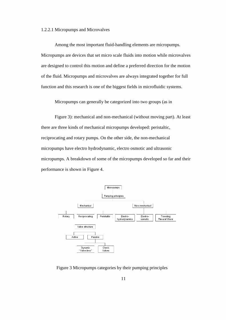
Micropumps can generally be categorized into two groups (as in
Figure 3): mechanical and non-mechanical (without moving part). At least
there are three kinds of mechanical micropumps developed: peristaltic,
reciprocating and rotary pumps. On the other side, the non-mechanical
micropumps have electro hydrodynamic, electro osmotic and ultrasonic
micropumps. A breakdown of some of the micropumps developed so far and their
performance is shown in Figure 4.
Figure 3 Micropumps categories by their pumping principles

12
Figure 4 Review of micropump technologies
Green represents mechanical micropumps, and pink non-mechanical
Table 2 Comparison of different actuation methods
Actuation method Pressure Displacement Response time
Disk type PZT Small Medium Fast
Stack type PZT Very large Very small Fast
Pneumatic Small Large Slow
Shape Memory Alloy Large Large Slow
Electrostatics Small Very small Very fast
Thermo-pneumatic Large Medium Medium
To date, the reciprocating displacement micropump has been the most
popular choice for researchers. This type of micropump generally comprises of a
pressure chamber bounded by a flexible diaphragm driven by an actuator and
passive or dynamic microvalves. The check valves and the actuator play very
important roles in the flow rate and the maximum output pressure. Many types of
actuators such as piezoelectric, pneumatic, electrostatic and thermo-pneumatic
have been used. The performance of active valves and micropumps depend
13
strongly on the features of the actuator. And the maximum pressure head
realizable by the micropump depends directly on the available force of the
actuator used (Table 2). Performance of micropump and microvalves are
described as follows.
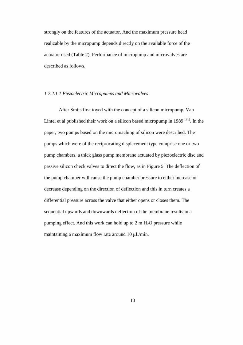
1.2.2.1.1 Piezoelectric Micropumps and Microvalves
After Smits first toyed with the concept of a silicon micropump, Van
Lintel et al published their work on a silicon based micropump in 1989 [21]
. In the
paper, two pumps based on the micromaching of silicon were described. The
pumps which were of the reciprocating displacement type comprise one or two
pump chambers, a thick glass pump membrane actuated by piezoelectric disc and
passive silicon check valves to direct the flow, as in Figure 5. The deflection of
the pump chamber will cause the pump chamber pressure to either increase or
decrease depending on the direction of deflection and this in turn creates a
differential pressure across the valve that either opens or closes them. The
sequential upwards and downwards deflection of the membrane results in a
pumping effect. And this work can hold up to 2 m H2O pressure while
maintaining a maximum flow rate around 10 μL/min.
14
Figure 5 Schematic of the first reciprocating displacement micropump
Soon after this, another silicon micropump was fabricated by M. Esashi in
1989 [22]
. The micromachined device contains a normally closed microvalve and a
diaphragm-type pump, which contains two polysilicon one-way valves and a
diaphragm driven by a small piezoelectric actuator. The maximum pumping flow
rate was 20 μL/min and pressure 0.78m H2O/cm2.
Despite the major disadvantage that these piezoelectrically driven pumps
need more than 100 V to drive, reciprocating micropumps, especially those based
on piezoelectric actuation still have grown to be the dominant type of micropump
and tremendous improvements have been made [23-26]
. Among them was the first
commercial micropump developed by IMT of Germany [27]
, a polycarbonate
micropump fabricated using microfabrication and conventional thermoplastic
replication technologies.
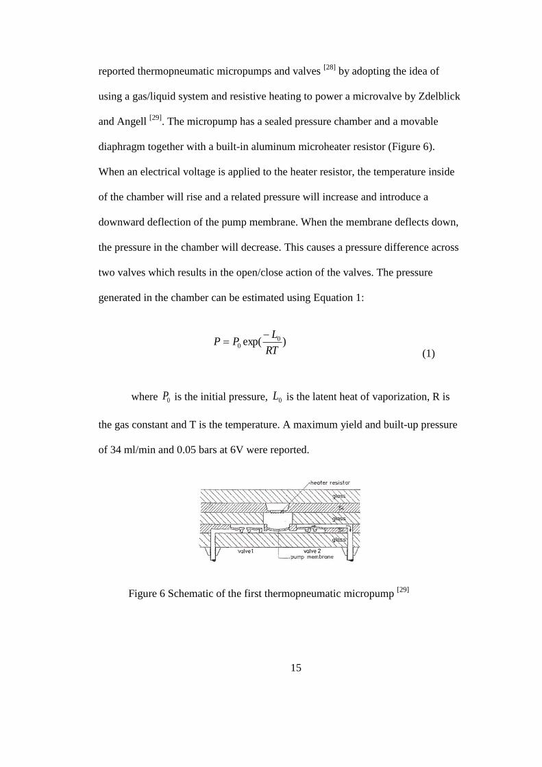
1.2.2.1.2 Thermopneumatic Micropumps and Microvalves
Before 1990, all the micropump prototypes developed usd piezoelectric
bimorph or monomorph discs for the actuation until F.C.M. Van De Pol et al
15
reported thermopneumatic micropumps and valves [28]
by adopting the idea of
using a gas/liquid system and resistive heating to power a microvalve by Zdelblick
and Angell [29]
. The micropump has a sealed pressure chamber and a movable
diaphragm together with a built-in aluminum microheater resistor (Figure 6).
When an electrical voltage is applied to the heater resistor, the temperature inside
of the chamber will rise and a related pressure will increase and introduce a
downward deflection of the pump membrane. When the membrane deflects down,
the pressure in the chamber will decrease. This causes a pressure difference across
two valves which results in the open/close action of the valves. The pressure
generated in the chamber can be estimated using Equation 1:
)exp( 0
0RT
LPP
(1)
where 0P is the initial pressure, 0L is the latent heat of vaporization, R is
the gas constant and T is the temperature. A maximum yield and built-up pressure
of 34 ml/min and 0.05 bars at 6V were reported.
Figure 6 Schematic of the first thermopneumatic micropump [29]

16
In recent research, S. Zimmermann et al developed a planar micropump
using a wafer-level, four-mask process, making it attractive for integration into the
micro-total-analysis system [30]
. It employs thermopneumatic actuation and two in-
plane flap valves (Figure 7 and Figure 8) with fluidic-resistance ratio greater than
1300 to reach maximum pressure of 16KPa and maximum flow rate of 9 μL/min
at an average power assumption of 180mW with a frequency of 10 Hz and 20%
duty cycle.
Figure 7 Photo of the planar micropump utilizing two platinum hearers for
thermopneumatic actuation and two in-plane flaps valves
Figure 8 Cross-sectional view of the valve seat showing that all leakage paths
around the valve seat are sealed
17
1.2.2.1.3 Electrostatic Micropumps and Microvalves
The first electrostatic actuated micropump was developed in 1991 [31]
. The
micropump consists of two identical microvalves joined to opposite sides of a
micro mechanical membrane by microchannels. The fabricated diagnostic chip
consists of various test arrays. One is composed of varying valve length and
microchannel width combinations, while another small test area consists of the
three sizes of membranes. The operation of this pump utilizes electrostatic forces
between movable parallel plate polysilicon conductors. The electrostatic forces
deform thin polysilicon cantilever valves and membranes to control fluids or gases
through narrow channels. Both the upper and lower electrodes are encapsulated by
LPCVD Si3Nr so that the electrodes will not electrically short when pumping
conductive fluids.
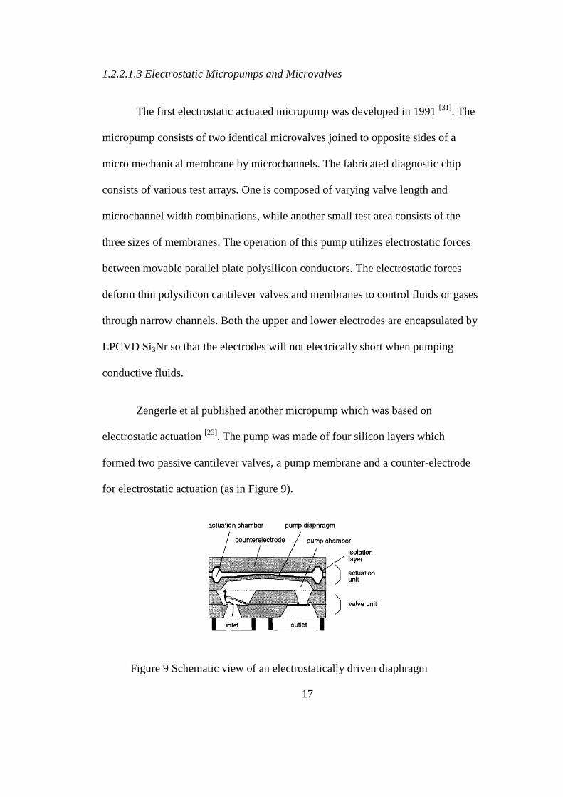
Zengerle et al published another micropump which was based on
electrostatic actuation [23]
. The pump was made of four silicon layers which
formed two passive cantilever valves, a pump membrane and a counter-electrode
for electrostatic actuation (as in Figure 9).
Figure 9 Schematic view of an electrostatically driven diaphragm
18
In the case of an electrostatically driven displacement unit the pump is
actuated by a square wave with an amplitude of 150 V - 200 V and frequencies of
0.1 Hz up to several hundred Hz. If the supply voltage is switched on, the pump
diaphragm is driven by electrostatic forces and bends towards the counter-
electrode. Thereby fluid will be sucked in through the inlet valve. When the
supply voltage is turned off, the relaxation of the diaphragm pushes the fluid
through the outlet valve. Two passive check valves direct the flow from inlet to
outlet and so, miniaturized diaphragm pumps are known as unidirectional pumps.
The outer dimensions of the electrostatically actuated diaphragm pump are 7 x 7 x
2 m3. The pump has achieved maximum pump rates of 850 μL/min and a
maximum hydrostatic back pressure of 310 hPa (310 cm H2O) at a supply voltage
of 200 V. The total power consumption of the pump element is less than 1 mW
and the strong electrostatic field is completely separated from the fluid.
1.2.2.1.4 Pneumatic Micropumps and Microvalves
Pneumatic actuation is not very popular due to its relative complexity in
terms of design and fabrication. However, Rapp et al’s research does need to be
mention here [32]
. By combining the LIGA technique with processes used in the
manufacture of micromembranes, micromembrane pumps have been built with
pump chambers 100 μm in height and with pump membrane diameters between 2
and 5 mm. The pump case is made of gold, whereas the 2.7 μm thin pump
membrane consists of titanium. The passive microvalves of the pump consist of
patterned micromembranes arranged one over the other and made of titanium and
19
polyimide by use of thin-film techniques. The micropump has been tested so far
with an external pneumatic drive. Both air and water have been pumped. A
maximum flow rate of 82μL/min and a maximum pressure of 0.47 m H2O were
obtained for pumping of air at a driving frequency of 5 Hz. The remarkable
achievement of Rapp’s micropumps is the utilization of thermoplastic
microreplication. It embarks the way of producing microstructure components in
high volume at low cost. It greatly increases the potential use of microstructures in
industry.
Most of the research about pneumatic micropumps followed after Rapp’s
work began to take the advantage of microreplication. Though the substrates vary
from silicon, glass to elastomer, most of diaphragms of the micropump design are
using polymeric materials to get flexible membranes. Grosjean et al [33]
chose
Parylene and silicone rubber, Meng [34]
et al use silicone rubber on their
thermoplastic construction, and lately in Grover’s design PDMS has been chosen
to make the diaphragm [35]
. Unger et al even proposed a multi-layered elastomeric
microstructure which is also pneumatic driven [16]
and this design shows the great
potential of microreplication and popularize the use of elastomeric microstructures
in microfluidic systems.
Other than the above micropumps, shape-memory alloys have been used to
develop a flap structure in Benard’s mechanical micropumps [36]
and
electromagnetic actuation was involved in both Dario [37]
and Bohm’s [38]
research
on micropumps.
20
As the research about microfluidic system moves on, more and more
attention is gathered on the applications in the biological and chemical analysis,
which gave a hand to the development of non-mechanical micropumps. In contrast
to mechanical micropumps, non-mechanical micropumps normally don’t have
either moving parts or valve. This simplifies the design and fabrication and brings
long life cycles and minimal risks of blockage. However, this kind of pumps
usually feasible only at microscale because the generated forces are generally too
small to move large amount of fluids unless increasing the input to 10 kV. In
addition, such pumps are restricted to certain types of pumping fluids. Examples
of such pumps include electrohydrodynamic (EHD), electroosmotic (EO) and
magnetohydrodynamic (MHD) pumps.
1.2.2.1.5 Electrohydrodynamic (EHD) Micropumps
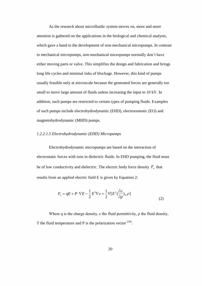
Electrohydrodynamic micropumps are based on the interaction of
electrostatic forces with ions in dielectric fluids. In EHD pumping, the fluid must
be of low conductivity and dielectric. The electric body force density eF that
results from an applied electric field E is given by Equation 2:
])([2
1
2
1 22
Tep
EEEPqEF
(2)
Where q is the charge density, ε the fluid permittivity, ρ the fluid density,
T the fluid temperature and P is the polarization vector [39]
.
21
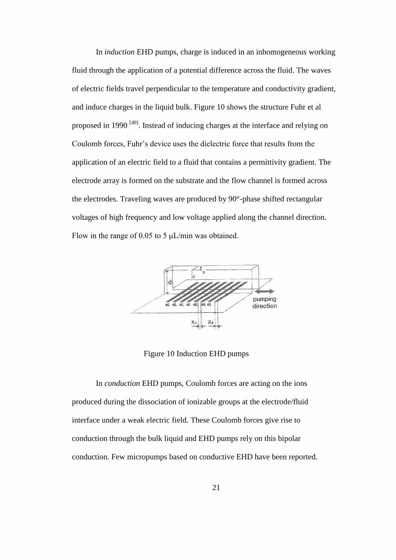
In induction EHD pumps, charge is induced in an inhomogeneous working
fluid through the application of a potential difference across the fluid. The waves
of electric fields travel perpendicular to the temperature and conductivity gradient,
and induce charges in the liquid bulk. Figure 10 shows the structure Fuhr et al
proposed in 1990 [40]
. Instead of inducing charges at the interface and relying on
Coulomb forces, Fuhr’s device uses the dielectric force that results from the
application of an electric field to a fluid that contains a permittivity gradient. The
electrode array is formed on the substrate and the flow channel is formed across
the electrodes. Traveling waves are produced by 90°-phase shifted rectangular
voltages of high frequency and low voltage applied along the channel direction.
Flow in the range of 0.05 to 5 μL/min was obtained.
Figure 10 Induction EHD pumps
In conduction EHD pumps, Coulomb forces are acting on the ions
produced during the dissociation of ionizable groups at the electrode/fluid
interface under a weak electric field. These Coulomb forces give rise to
conduction through the bulk liquid and EHD pumps rely on this bipolar
conduction. Few micropumps based on conductive EHD have been reported.
22
EHD micropumps based on the injection of ions into the working fluid at
electrodes have also been reported. For specific electrode/liquid interfaces,
application of a very high electric field, greater than 100kV/cm, injects ions to
into the bulk fluid. The Coulomb force acts on the injected charges; viscous
interaction generates bulk flow. Richter et al reported a micromachined EHD
micropump based on injection [41]
. Driven by a 600V electric field, this
micropump pumps ethyl alcohol with a maximum flow rate of 14mL/min and
maximum pressure of 2.5kPa.
1.2.2.1.6 Electroosmotic (EO) Micropumps
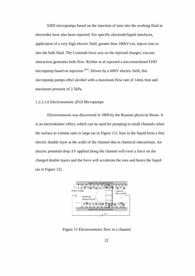
Electroosmosis was discovered in 1809 by the Russian physicist Reuss. It
is an electrokinetic effect, which can be used for pumping in small channels when
the surface to volume ratio is large (as in Figure 11). Ions in the liquid form a thin
electric double layer at the walls of the channel due to chemical interactions. An
electric potential drop ∆V applied along the channel will exert a force on the
charged double layers and the force will accelerate the ions and hence the liquid
(as in Figure 12).
Figure 11 Electroosmotic flow in a channel
23
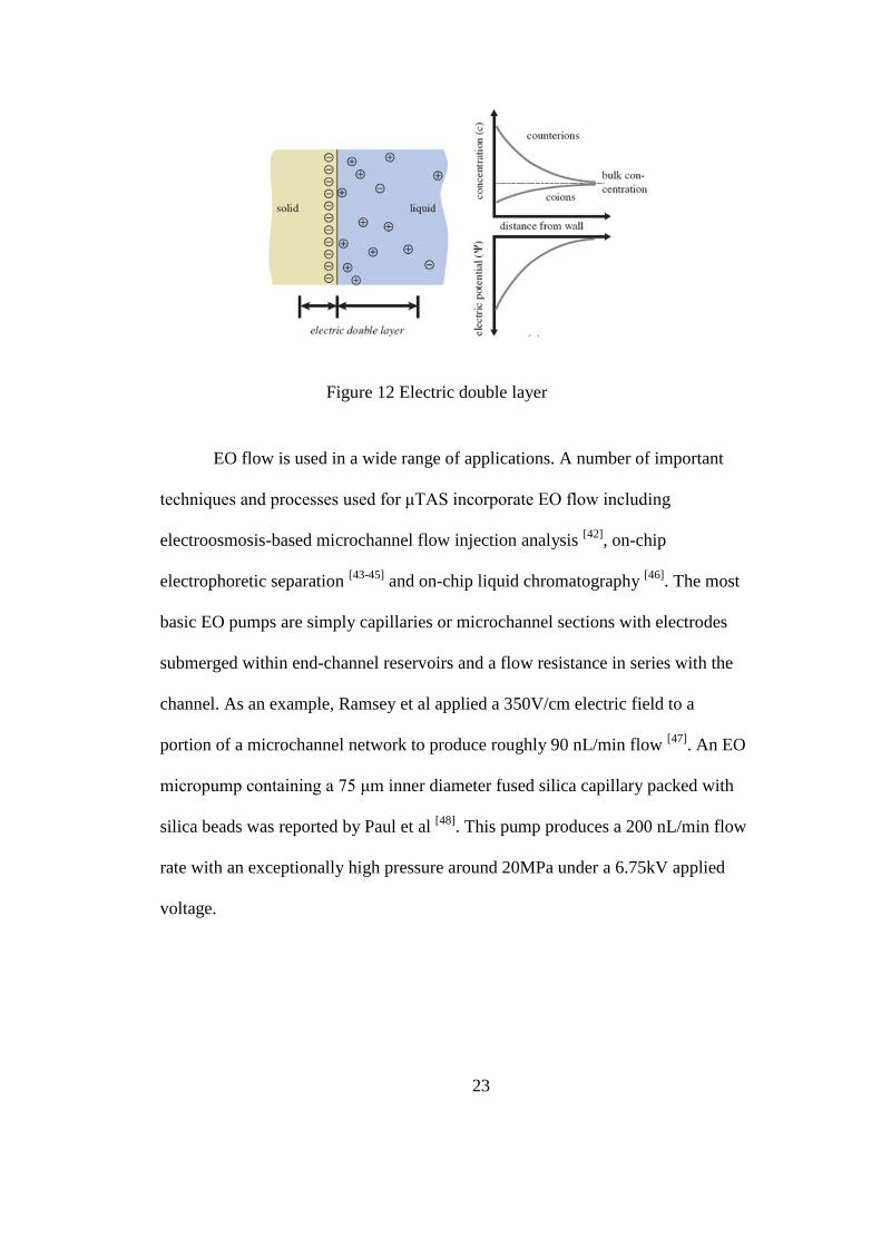
Figure 12 Electric double layer
EO flow is used in a wide range of applications. A number of important
techniques and processes used for μTAS incorporate EO flow including
electroosmosis-based microchannel flow injection analysis [42]
, on-chip
electrophoretic separation [43-45]
and on-chip liquid chromatography [46]
. The most
basic EO pumps are simply capillaries or microchannel sections with electrodes
submerged within end-channel reservoirs and a flow resistance in series with the
channel. As an example, Ramsey et al applied a 350V/cm electric field to a
portion of a microchannel network to produce roughly 90 nL/min flow [47]
. An EO
micropump containing a 75 μm inner diameter fused silica capillary packed with
silica beads was reported by Paul et al [48]
. This pump produces a 200 nL/min flow
rate with an exceptionally high pressure around 20MPa under a 6.75kV applied
voltage.

24
Operation voltages and geometries of EO pumps vary widely. A detailed
description of the history and development of EO pumps is presented by Yao and
Santiago [49]
.
1.2.2.1.7 Magnetohydrodynamic (MHD) Micropumps
Magnetohydrodynamic refers to the flow of electrically conducting liquids
in electric and magnetic fields. The typical structure of a MHD pump has been
drawn in Figure 13[50]
. It is comprised of microchannels with two walls bounded
by electrodes to generate the electric field while the other two walls are bound by
permanent magnets of opposite polarity to generate the magnetic field. Lorentz
force is the pumping source in the conductive, aqueous solution in MHD
micropumps in the direction perpendicular to both magnetic and electric fields.
This actuation is similar to EHD micropumps.
Figure 13 Schematic diagram of the actuation principle of the MHD
micropump where driving force is Lorentz force
Jang and Lee reported an MHD micropump with a 40 nm long
microchannel with a hydraulic diameter around 1mm. With permanent magnets
producing a magnetic flux density 0.44 T and a total current 1~100 μA, this pump
25
can reach a maximum flow rate of 62 μL/min with a pressure of 170Pa[50]
. Lemoff
and Lee used a miniature electromagnetic coil operation at 1kHz to avoid
electrolysis associated with DC citation [51]
. A 1 M NaCl solution was pumped
using this pump at a flow rate of 18 μL/min.
Compared with other types of non-mechanical micropumps, the MHD
micropump has several advantages, such as simple fabrication process, bi-
directional pumping ability, and its suitability in pumping of conductive fluids
which EHD and EO micropumps have limits on.
In summary, flow rate, pressure generation and overall size are important
figures of merits for micropumps. The EO micropumps and PZT-driven
reciprocating displacement micropumps perform well in terms of absolute flow
rate and pressure generation and exhibit comparable performance. Though
thermopneumatic micropumps tend to produce low flow rate, the application of
microreplication make these kinds of micropumps still very hot among researchers.
Given the comparatively high self-pumping frequency and small size of
Zengerle’s electrostatically driven micropump, further research on electrostatic
actuation for micropumps is needed. Since the first micropump was introduced in
the early 1980s, progress and development have been moving rapidly. As
micropumps continue to improve, we can expect that micropumps will be
increasingly used in a wide variety of microfluidic systems in fields including life
science, semiconductors and even space exploration.
26
1.2.2.2 Channels in Microfluidic System
Another important component in microfluidic systems is the microchannel.
In any microfluidic system, microchannels serve as pipes in the form of either a
single channel or a network. Different cross sections of microchannels
(rectangular, circular, trapezoidal, triangular and elliptical) have been studied by
several researchers to help understand the flow behavior inside the channels.
Among them, rectangular and trapezoidal cross-sections have been extensively
studied for a wide variety of applications due to practical considerations such as
fabrication techniques, cost and ease of manufacturing, etc. In most of the
research about different physical phenomena at the micro level, friction and
pressure drop [52]
, electroviscous effect [53]
, velocity measurement [54]
, flow
control[55]
and flow visualization [56]
, rectangular cross-section microchannels are
employed. Some new design using trapezoidal cross-sections proposed during this
microchannel study. Ross et al [57]
choose trapezoidal shape microchannels to
study sample dispersion in electroosmotic flows in plastic microchannels. The
frictional and pressure drop characteristics in trapezoidal microchannels were
studied by several researchers [58-60]
. Circular cross-sections are mainly limited to
heat transfer equipment such as microheatexchanger. In the mean time, half-
circular cross-section microchannels proposed in Quake’s paper demonstrate a
better seal for the membrane valve, which is a very critical requirement for a
microfluidic system.
27
A diversity of fluid properties and microfluidic device applications is
translated into a wide variety of requirements in microscale flow control in
microchannels. For example, the position streams within the cross-section of the
microchannel for precise delivery of reagents, the mixing of solutions for
chemical reactions and the transportation of small amounts of solution for high
throughput synthesis and analysis are all need the support of flow control in the
channels. With the technology of patterned surface charges and electrodes used
for manipulating electroosmotic flow, patterned wettibility and peristalsis for
control of pressure driven and patterned topography for both of these two flows,
the various mechanisms implied by these technologies have been used to control
dispersion, mixing and pumping, etc.
There are so many possible areas of research in the field of microfluidic.
Microfluidics has emerged as a distinct new field and has attracted attention
recently past due to the many applications in biotechnology. As microfluidic
continue to evolve, it will be important to have portable applications that can run
on successive generations of chips. And that also is the reason why the
progressive miniaturization of chemical and biological instrumentation towards
creating highly integrated “lab-on-chip” system or μTAS systems has always been
the most exciting scientific developments of recent years.
1.3 Introduction of Deformable Micromirrors for Adaptive Optics
Adaptive optics is the control of optical wavefront phase in a real-time,
closed-loop fashion. It has been mainly used in astronomical applications to
28
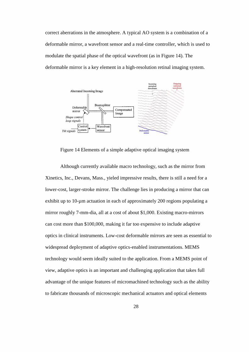
correct aberrations in the atmosphere. A typical AO system is a combination of a
deformable mirror, a wavefront sensor and a real-time controller, which is used to
modulate the spatial phase of the optical wavefront (as in Figure 14). The
deformable mirror is a key element in a high-resolution retinal imaging system.
Figure 14 Elements of a simple adaptive optical imaging system
Although currently available macro technology, such as the mirror from
Xinetics, Inc., Devans, Mass., yieled impressive results, there is still a need for a
lower-cost, larger-stroke mirror. The challenge lies in producing a mirror that can
exhibit up to 10-µm actuation in each of approximately 200 regions populating a
mirror roughly 7-mm-dia, all at a cost of about $1,000. Existing macro-mirrors
can cost more than $100,000, making it far too expensive to include adaptive
optics in clinical instruments. Low-cost deformable mirrors are seen as essential to
widespread deployment of adaptive optics-enabled instrumentations. MEMS
technology would seem ideally suited to the application. From a MEMS point of
view, adaptive optics is an important and challenging application that takes full
advantage of the unique features of micromachined technology such as the ability
to fabricate thousands of microscopic mechanical actuators and optical elements
29
(including lenses, lasers and sensors) on a single silicon chip and the potential
integration of this micromachined optical bench with control circuits and imaging
sensors.
Dr. Larry J. Hornbeck at Texas Instruments first invented a micromirror
which is a reflective spatial light modulator monolithically fabricated over an
address circuit consisting of conventional CMOS SRAM cells [61]
. The
micromirror is actuated by electrostatic force which is generated by applying a
voltage difference between the mirror plate and the electrode. Light from a
projection source illuminates the micro mirror array at an angle of ±2θL from the
normal to the plane of mirrors in their flat state. The angle 2θL is the rotation
angle of the mirror when the yoke is touching its mechanical stops, or landed. The
mirror in its flat state reflects the incident light to an angle of -2θL. The
projection lens is designed so that flat state light misses the pupil of the projection
lens, allowing very little light to be projected through the lens. But the mirrors are
only briefly at the flat state as they make a transition from one landed state to the
other. When the mirror is in its off state, the reflected light is further removed
from the pupil of the projection lens and even less light is collected by the
projection lens. When the mirror is in its on state, the reflected light is directed
into the pupil of the projection lens, and nearly all the light is collected by the
projection lens and imaged to the projection screen. Because of the large rotation
angles of the mirror, the off-state light and on-state light are widely separated,
allowing fast projection optics to be used. The result is efficient light collection
while maintaining a high contrast ratio.
30
Three types of deformable micromirrors are currently being investigated:
continuous face sheet mirrors backed by individual actuating elements,
microfabricated membranes mirrors and segmented mirrors.
Continuous face sheet mirror backed by individual actuating elements
have been demonstrated to be particularly well suited for high power laser
application [62]
.
Figure 15 Schematic of Stanford continuous membrane mirror
The shape of the face sheet is controlled by a number of discrete actuators
that are fixed to its back [62]
. The shape of the mirror depends on the combination
of forces applied to the face sheet, boundary conditions (the way the face sheet is
fixed to the mirror) and the geometry and the material of the face sheet. These
mirrors are considered to be the best, as they allow smooth wavefront control with
very large - up to several thousand - degrees of freedom. The good surface quality
leads to good reflectivity, which is very important for high power applications.
Microfabricated membrane mirrors have high optical efficiency and a
very good potential for aberrations correction, while keeping small dimensions.
The membrane can be deformed electrostatically by applying control voltages to
31
the electrostatic electrode actuators that can be positioned under the membrane
and also over the membrane. If there are any electrodes positioned over the
membrane, they should be transparent. It is possible to operate the mirror with
only one group of electrodes positioned under the mirror. In this case a bias
voltage should be applied to all electrodes, to make the membrane initially
spherical. The membrane can move back and forth with respect to the reference
sphere. These properties make them very suitable for optical fiber switching
applications. A microfabricated membrane mirror has been used to optimize the
coupling efficiency for an optical fiber switch for more than 3000 interconnects.
Segmented deformable mirrors are formed by independent flat mirror
segments. Each segment can move a small distance back and forward (a pure
piston motion) to approximate the average value of the wavefront over the patch
area. Normally these mirrors have little or zero cross-talk between actuators.
Stepwise approximation works poorly for smooth continuous wavefront. Sharp
edges of the segments and gaps between the segments contribute to the light
scattering, limiting the applications to those non-sensitive to scattered light.
Considerable improvement in the approximation performance of the segmented
mirror can be achieved by introducing three degrees of freedom per segment:
piston tip and tilt. These mirrors require three times more actuators than piston
segmented mirrors and they suffer from diffraction on the segment edges. This
concept was used in the fabrication of large segmented primary mirrors of Keck
telescopes. Segmented mirrors are fast, due their small size. Typically, a single
pixel is 100μm aside. Their reliability, small size, light weight and ease of

32
fabrication make them particularly well suited for free space optical
communication.
Deformable micromirror was first proposed in 1986 [63]
with a layer of
deformable viscoelastic reflective material with electrostatically driven light
valves. The principle of operation is shown in Figure 16.
Figure 16 Principle of operation of deformable viscoelastic mirror
On top of the substrate carrying the pixel electrodes there is a viscoelastic
control layer covered with a mirror electrode. A bias voltage, U0, of typically
250V, is applied between the pixel electrodes and the mirror electrode whereby
the reflective viscoelastic layer behaves like a plane mirror. Upon applying a
signal voltage, Us, of about ±15V to neighboring pixel electrodes the viscoelastic
mirror is deformed sinusoidally forming a phase grating corresponding to the
active pixels. Kuck H et al fabricated deformable micromirror devices using
PDMS as its viscoelastic layer [64]
.
33
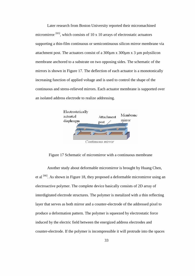
Later research from Boston University reported their micromachined
micromirror [65]
, which consists of 10 x 10 arrays of electrostatic actuators
supporting a thin-film continuous or semicontinuous silicon mirror membrane via
attachment post. The actuators consist of a 300µm x 300µm x 3 µm polysilicon
membrane anchored to a substrate on two opposing sides. The schematic of the
mirrors is shown in Figure 17. The deflection of each actuator is a monotonically
increasing function of applied voltage and is used to control the shape of the
continuous and stress-relieved mirrors. Each actuator membrane is supported over
an isolated address electrode to realize addressing.
Figure 17 Schematic of micromirror with a continuous membrane
Another study about deformable micromirror is brought by Huang Chen,
et al [66]
. As shown in Figure 18, they proposed a deformable micromirror using an
electroactive polymer. The complete device basically consists of 2D array of
interdigitated electrode structures. The polymer is metalized with a thin reflecting
layer that serves as both mirror and a counter-electrode of the addressed pixel to
produce a deformation pattern. The polymer is squeezed by electrostatic force
induced by the electric field between the energized address electrodes and
counter-electrode. If the polymer is incompressible it will protrude into the spaces
34
between the energized electrodes. The result is a diffraction grating effect on the
energized pixel. The polymer surface of the non-energized pixel remains flat.
Gray scale is achieved by varying the voltage on the address electrodes.
Figure 18 Electroactive polymer deformable micromirror
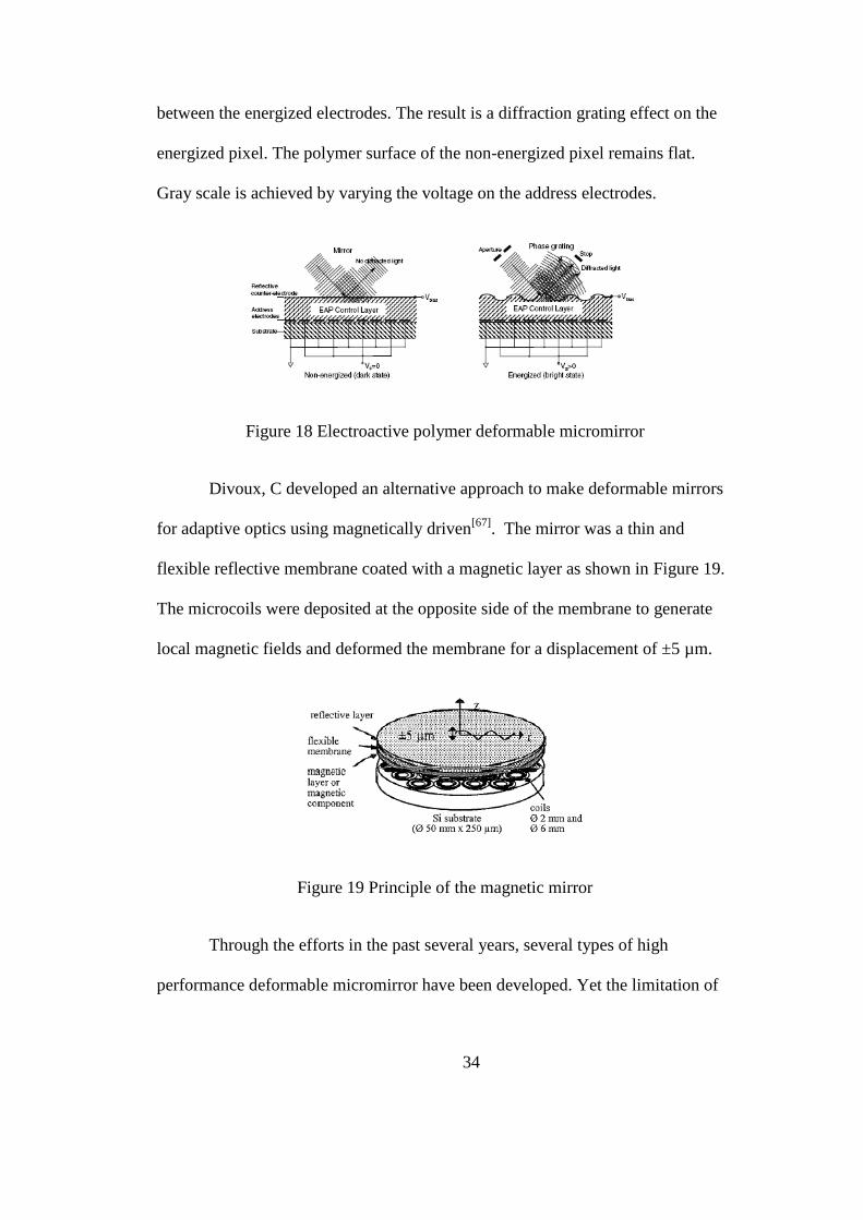
Divoux, C developed an alternative approach to make deformable mirrors
for adaptive optics using magnetically driven[67]
. The mirror was a thin and
flexible reflective membrane coated with a magnetic layer as shown in Figure 19.
The microcoils were deposited at the opposite side of the membrane to generate
local magnetic fields and deformed the membrane for a displacement of ±5 µm.
Figure 19 Principle of the magnetic mirror
Through the efforts in the past several years, several types of high
performance deformable micromirror have been developed. Yet the limitation of
35
small displacement or deformation in current achievements restricts the growth of
adaptive optics’ applications. A good choice of soft material to provide larger
deformation for mirrors would great benefit this demand. The flexibility of
fabrication and integration of polymer materials such as PDMS reduced
significantly the cost of the mirrors and combining with the advantage brought by
MEMS technology, it is easy to expect that micromirrors would be as popular and
in such demand as car airbag MEMS sensors.
1.4 PDMS and Soft Lithography
PDMS has been widely used in fabricating lab-on-a-chip or Micro Total
Analysis Systems (µTAS), due to its unique properties, like optically transparent,
easy in fabrication, and cheap. Most important of all, its biocompatibility is
critical for biological assays. PDMS is optically transparent to wavelengths close
to 256nm [68]
. This transparent nature is well suited for biological analysis using
visual techniques such as fluorescence, and facilitates on- and off-chip detection.
PDMS’s elastic and soft nature makes it easy for reversible deformations [69]
.
µTAS [70-72]
system made of PDMS can be realized by molding, casting or soft
lithography with high fidelity [73-76]
. PDMS can seal to itself and other flat surface
with a good watertight capability. Meanwhile, the fabrication of µTAS or other
micro-devices are cost effective, which suits the disposable nature of most bio-
medical applications [77, 78]
. Based on these characteristics, PDMS appears to be
highly interesting as a bio-MEMS material and the potential to utilize PDMS for a
number of biochips increases[79]
.
36
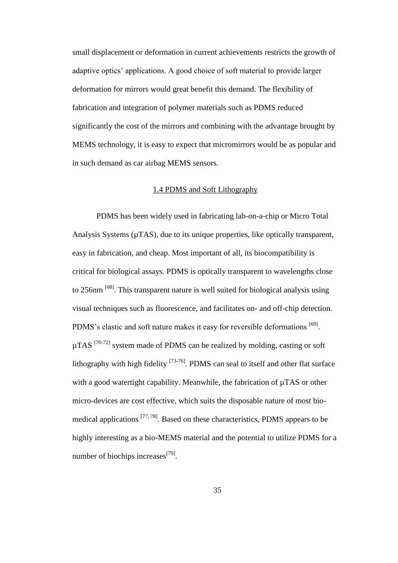
1.3.1 Introduction of PDMS
PDMS (polydimethylsiloxane) normally contains a base polymer (part A),
siloxane oligomer and a curing agent (part B), siloxane cross-linker. Once mixed
at a weight ratio of 10A:1B, poured over the master, and heated to elevated
temperatures, the liquid mixture of these two parts at specific weight ratios will
become a solid, cross-linked elastomer in a few hours. When mixing patios are
controlled during fabrication, two different PDMS parts can be bonded tightly as
one part without any material properties change or using conventional plasma
treating method [77]
. This PDMS specialty makes multiple layers soft lithography
possible to make 3-Dimentional MEMS devices.
The chemical formula for PDMS is (CH3)3SiO [SiO(CH3)2]nSi(CH3)3,
where n is the number of repeating monomer [SiO(CH3)2] units, as shown in
Figure 20. During the curing process, the hydrosilylation reaction happens
between vinyl (SiCH=CH2) groups and hydrosilane (SiH) groups. The surface of
PDMS in its natural state is hydrophobic.
Figure 20 Chemical formulas of PDMS
37
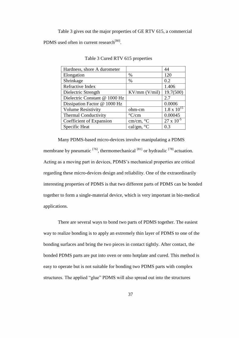
Table 3 gives out the major properties of GE RTV 615, a commercial
PDMS used often in current research[80]
.
Table 3 Cured RTV 615 properties
Hardness, shore A durometer 44
Elongation % 120
Shrinkage % 0.2
Refractive Index 1.406
Dielectric Strength KV/mm (V/mil) 19.7(500)
Dielectric Constant @ 1000 Hz 2.7
Dissipation Factor @ 1000 Hz 0.0006
Volume Resistivity ohm-cm 1.8 x 10¹⁵
Thermal Conductivity °C/cm 0.00045
Coefficient of Expansion cm/cm, °C 27 x 10-5
Specific Heat cal/gm, °C 0.3
Many PDMS-based micro-devices involve manipulating a PDMS
membrane by pneumatic [76]
, thermomechanical [81]
or hydraulic [78]
actuation.
Acting as a moving part in devices, PDMS’s mechanical properties are critical
regarding these micro-devices design and reliability. One of the extraordinarily
interesting properties of PDMS is that two different parts of PDMS can be bonded
together to form a single-material device, which is very important in bio-medical
applications.
There are several ways to bond two parts of PDMS together. The easiest
way to realize bonding is to apply an extremely thin layer of PDMS to one of the
bonding surfaces and bring the two pieces in contact tightly. After contact, the
bonded PDMS parts are put into oven or onto hotplate and cured. This method is
easy to operate but is not suitable for bonding two PDMS parts with complex
structures. The applied “glue” PDMS will also spread out into the structures
38
instead of just the bonding surface. The bonding layer will also change the
original thickness of the device structures, which may be a very critical
requirement. Another disadvantage of this method is that, it is easy to trap air
bubbles when bringing the two surfaces into contact. High pressure is required to
remove the bubble between the two pieces when contacting. Oxygen plasma
treatment can overcome the bubble trapping problem of the previous method.
PDMS is a hydrophobic polymer for which exposure to oxygen plasma leads to
oxidation and chain scission as well as cross-linking and the formation of a silica-
like surface [77]
. Oxygen plasma treatment can bond PDMS with not only itself but
also glass, silicon and other flat surfaces. The downside to this method is that
PDMS cannot maintain this state for more than 10 minutes and will reveal back to
its natural state. This problem is made worse by the fact that the equipment cost of
oxygen plasma is high. Quake et al developed another method to bond PDMS
parts [16]
. They utilized the feature that different mixing ratios can result in
different properties of PDMS to realize bonding between two parts with different
mixing ratios. By re-curing the two parts together under heat, two PDMS parts can
be bonded into one part. This method is cost-effective and no expensive
equipment is required. Also because the chemical components in the two parts are
the same, the whole device will be made of a single-material, which is great for
bioMEMS design.
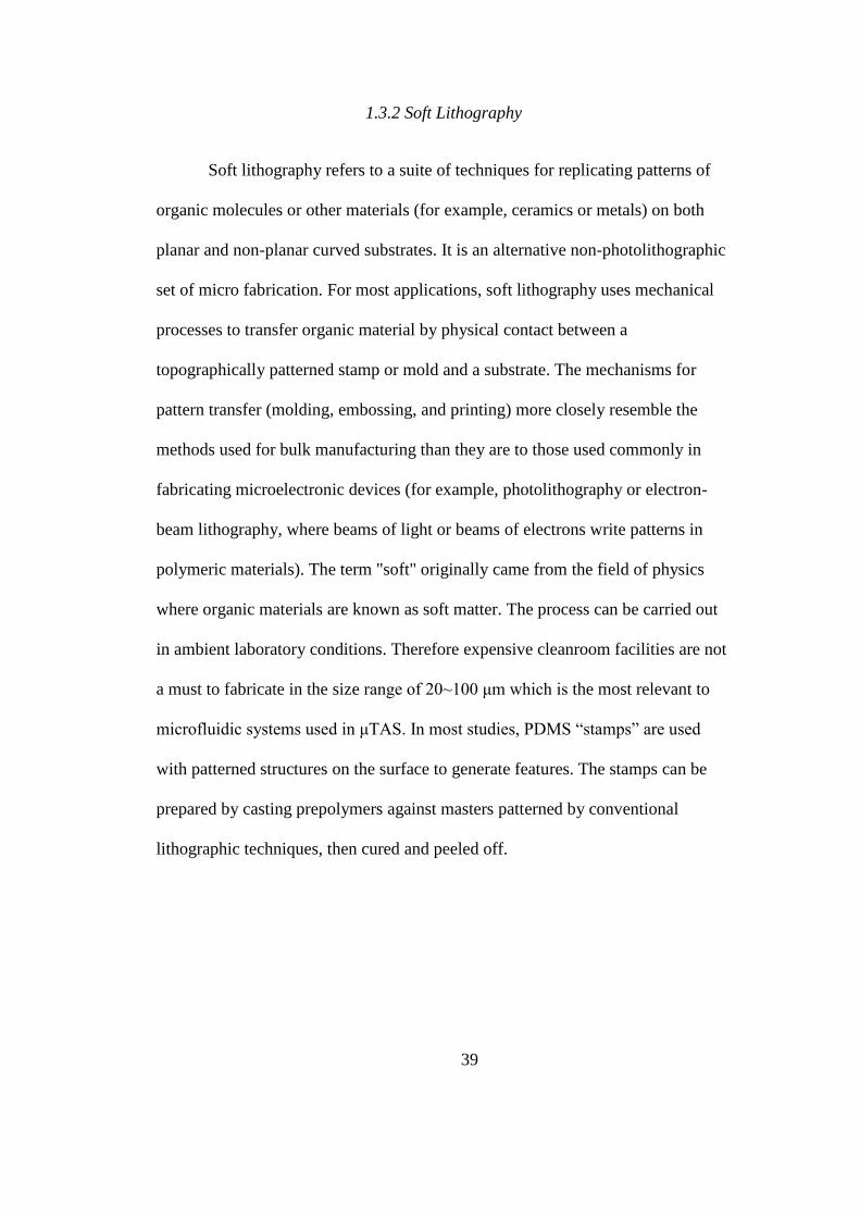
39
1.3.2 Soft Lithography
Soft lithography refers to a suite of techniques for replicating patterns of
organic molecules or other materials (for example, ceramics or metals) on both
planar and non-planar curved substrates. It is an alternative non-photolithographic
set of micro fabrication. For most applications, soft lithography uses mechanical
processes to transfer organic material by physical contact between a
topographically patterned stamp or mold and a substrate. The mechanisms for
pattern transfer (molding, embossing, and printing) more closely resemble the
methods used for bulk manufacturing than they are to those used commonly in
fabricating microelectronic devices (for example, photolithography or electron-
beam lithography, where beams of light or beams of electrons write patterns in
polymeric materials). The term "soft" originally came from the field of physics
where organic materials are known as soft matter. The process can be carried out
in ambient laboratory conditions. Therefore expensive cleanroom facilities are not
a must to fabricate in the size range of 20~100 μm which is the most relevant to
microfluidic systems used in μTAS. In most studies, PDMS “stamps” are used
with patterned structures on the surface to generate features. The stamps can be
prepared by casting prepolymers against masters patterned by conventional
lithographic techniques, then cured and peeled off.
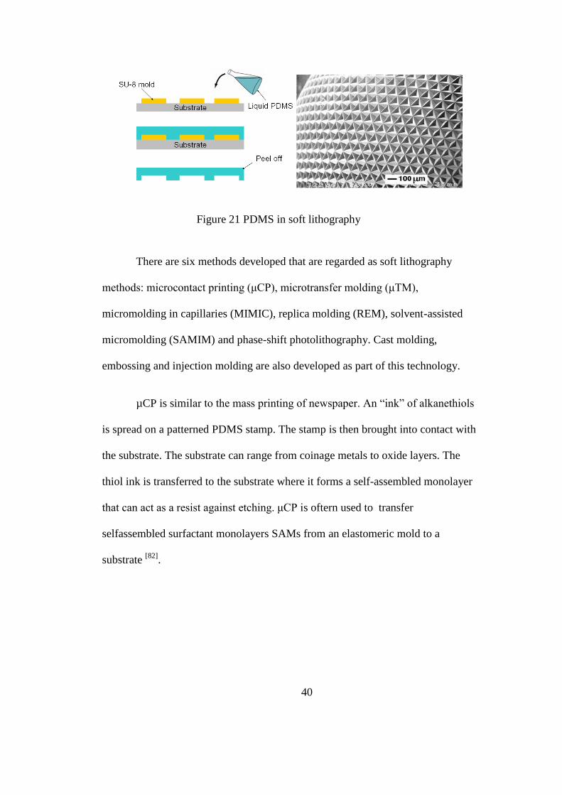
40
Figure 21 PDMS in soft lithography
There are six methods developed that are regarded as soft lithography
methods: microcontact printing (μCP), microtransfer molding (μTM),
micromolding in capillaries (MIMIC), replica molding (REM), solvent-assisted
micromolding (SAMIM) and phase-shift photolithography. Cast molding,
embossing and injection molding are also developed as part of this technology.
µCP is similar to the mass printing of newspaper. An “ink” of alkanethiols
is spread on a patterned PDMS stamp. The stamp is then brought into contact with
the substrate. The substrate can range from coinage metals to oxide layers. The
thiol ink is transferred to the substrate where it forms a self-assembled monolayer
that can act as a resist against etching. μCP is oftern used to transfer
selfassembled surfactant monolayers SAMs from an elastomeric mold to a
substrate [82]
.
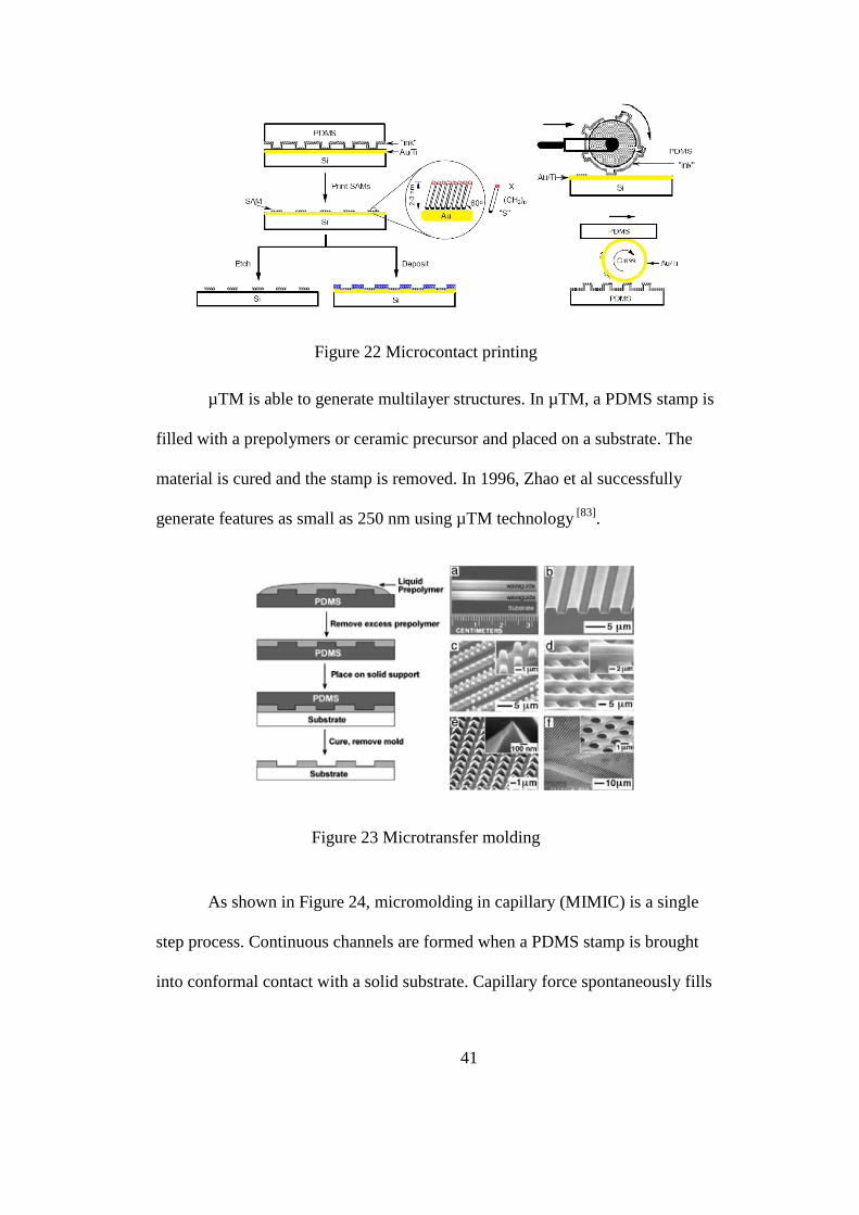
41
Figure 22 Microcontact printing
µTM is able to generate multilayer structures. In µTM, a PDMS stamp is
filled with a prepolymers or ceramic precursor and placed on a substrate. The
material is cured and the stamp is removed. In 1996, Zhao et al successfully
generate features as small as 250 nm using µTM technology [83]
.
Figure 23 Microtransfer molding
As shown in Figure 24, micromolding in capillary (MIMIC) is a single
step process. Continuous channels are formed when a PDMS stamp is brought
into conformal contact with a solid substrate. Capillary force spontaneously fills
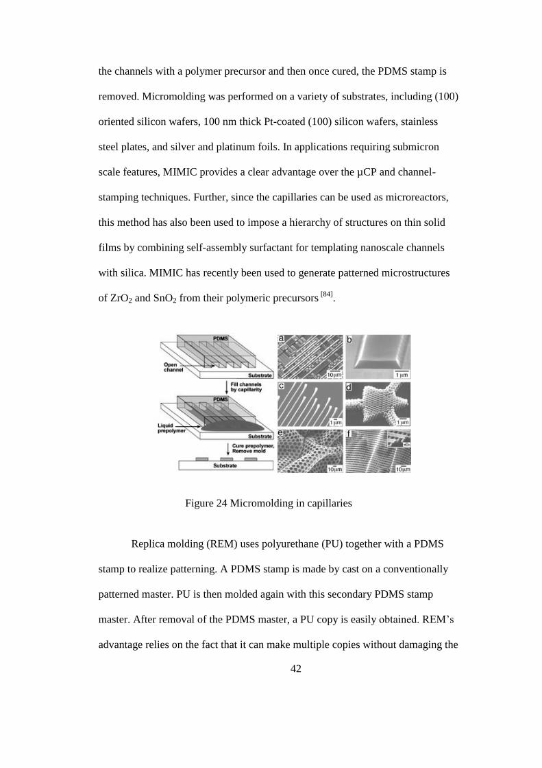
42
the channels with a polymer precursor and then once cured, the PDMS stamp is
removed. Micromolding was performed on a variety of substrates, including (100)
oriented silicon wafers, 100 nm thick Pt-coated (100) silicon wafers, stainless
steel plates, and silver and platinum foils. In applications requiring submicron
scale features, MIMIC provides a clear advantage over the µCP and channel-
stamping techniques. Further, since the capillaries can be used as microreactors,
this method has also been used to impose a hierarchy of structures on thin solid
films by combining self-assembly surfactant for templating nanoscale channels
with silica. MIMIC has recently been used to generate patterned microstructures
of ZrO2 and SnO2 from their polymeric precursors [84]
.
Figure 24 Micromolding in capillaries
Replica molding (REM) uses polyurethane (PU) together with a PDMS
stamp to realize patterning. A PDMS stamp is made by cast on a conventionally
patterned master. PU is then molded again with this secondary PDMS stamp
master. After removal of the PDMS master, a PU copy is easily obtained. REM’s
advantage relies on the fact that it can make multiple copies without damaging the
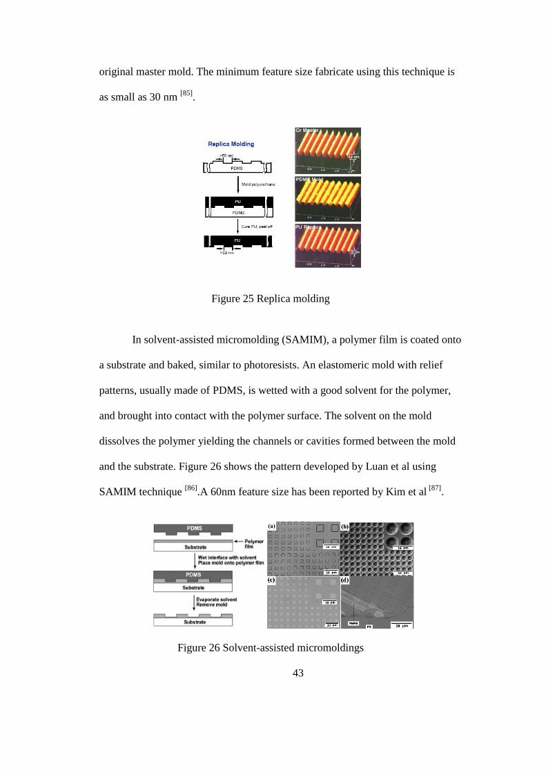
43
original master mold. The minimum feature size fabricate using this technique is
as small as 30 nm [85]
.
Figure 25 Replica molding
In solvent-assisted micromolding (SAMIM), a polymer film is coated onto
a substrate and baked, similar to photoresists. An elastomeric mold with relief
patterns, usually made of PDMS, is wetted with a good solvent for the polymer,
and brought into contact with the polymer surface. The solvent on the mold
dissolves the polymer yielding the channels or cavities formed between the mold
and the substrate. Figure 26 shows the pattern developed by Luan et al using
SAMIM technique [86]
.A 60nm feature size has been reported by Kim et al [87]
.
Figure 26 Solvent-assisted micromoldings

44
In phase-shift photolithography, a transparent PDMS phase mask with
relief structures on its surface is placed in conformal contact with a layer of
photoresist. Light passing through the stamps is modulated in the near-field. If the
relief on the surface of the stamp shifts the phase of light by an odd multiple, a
node in the intensity is produced. Features with dimensions between 40 and 100
nm are produced in the photoresist at each phase edge [88]
.This technique is best
suited for the fabrication of narrow electrode gap SAW devices that are designed
for the efficient SAW excitation at higher harmonics. The combination of near-
field phase shift lithography with narrow-gap SAW designs thus opens up a way
for simple and low-cost SAW devices operating above 5 GHz [89]
.
Figure 27 Phase-shift photolithography
Soft lithography appears to be a promising route to micro- or even nano-
structures in µTAS. Combining advanced microfabrication techniques, soft
lithography can easily transfer structures into organic polymers or other materials.
It provides researchers a convenient, effective and inexpensive way to make
μTAS with good biocompatibility. Soft lithography’s advantages, patterning on
non-polar surfaces, patterning of solid materials other than photoresists, patterning

45
over large area and three dimensional fabrications, will make this technique
become extremely competitive and widely used.
Considering PDMS’s many advantages, including low costs, short
fabrication time, biocompatibility, transparency, and combining the feasibility of
making devices using soft lithography, this technology is currently moving
forward rapidly and PDMS-based microfluidic systems are indeed a growing area
of interests.
46
CHAPTER 2 PROGRAMMABLE MICROFLUIDIC SYSTEM
2.1 Introduction
Advances in microfluidics technology are revolutionizing molecular
biology procedures for enzymatic analysis, DNA analysis (e.g., Polymerase chain
reaction and sequencing), and proteomics. The basic idea of microfluidic biochips
is to integrate assay operations such as detection, as well as sample pre-treatment
and preparation on one chip. The microfluidic systems on the “chip” perform as
small platforms comprising channel systems connected to liquid reservoirs by
tubing systems linked to syringes. The channel measures in the range of a few
micrometers, which greatly facilitates the handling of volumes much smaller than
a microliter. As microfluidic systems continue to evolve, it will be important to
have portable application codes that can run without modification on successive
generations of chips.
Though restricted by the traditional IC fabrication technology, silicon-
based microfluidic systems reveal their disadvantages like high cost and non-
biocompatibility to those bio-applications with the rising demand of bio-analysis.
Microfluidic research is focusing on the fabrication of a low cost and
biocompatible microfluidic system. PDMS stepped on this stage in the 1990’s. Its
great elastomeric properties and simplicity in fabrication enable the expanding of
microfluidic systems’ application field and bring more and more multidisciplinary
integrations as a total analysis system. Integrated with polymeric soft lithography,
the potential advances of PDMS-based microfluidic systems are huge: mass
47
produced disposable microfluidic chips that make anything from drug in vitro
delivery to biosensor detection possible.
Quake et al developed a multilayer soft lithography (MSL) that enabled
facile and inexpensive large scale integration of valves on a chip[16]
. It brought the
possibility of integrating a thin flexible elastomeric membrane to a monolithic
PDMS chip. This method greatly impacted by introducing a mechanical
microvalve with a structure that can provide function as a microvalve and act as
the foundation for the integrated micropumps and micromixers. A wide variety of
microfluidic systems have been developed based on a similar idea. Micropumps,
microvalves, micromixers, sensors and detectors are all integrated on a chip.
2.2 Design and Simulation
The proposed design develops a PDMS-based microfluidic system which
can provide a universal platform for different application of microfluidic systems
where microflow control is needed, no matter it is used in chemical or biological
analysis. The proposed microfluidic system uses both thermal pneumatic and
electrostatic actuation to realize the action and control of the microvalve and flow
in the microchannel. At the same time, the proposed design can be integrated into
a deformable micromirror array. The system will be made mainly of PDMS,
therefore, both photolithography and soft lithography will be used as fabrication
methods.
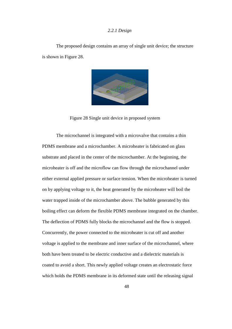
48
2.2.1 Design
The proposed design contains an array of single unit device; the structure
is shown in Figure 28.
Figure 28 Single unit device in proposed system
The microchannel is integrated with a microvalve that contains a thin
PDMS membrane and a microchamber. A microheater is fabricated on glass
substrate and placed in the center of the microchamber. At the beginning, the
microheater is off and the microflow can flow through the microchannel under
either external applied pressure or surface tension. When the microheater is turned
on by applying voltage to it, the heat generated by the microheater will boil the
water trapped inside of the microchamber above. The bubble generated by this
boiling effect can deform the flexible PDMS membrane integrated on the chamber.
The deflection of PDMS fully blocks the microchannel and the flow is stopped.
Concurrently, the power connected to the microheater is cut off and another
voltage is applied to the membrane and inner surface of the microchannel, where
both have been treated to be electric conductive and a dielectric materials is
coated to avoid a short. This newly applied voltage creates an electrostatic force
which holds the PDMS membrane in its deformed state until the releasing signal
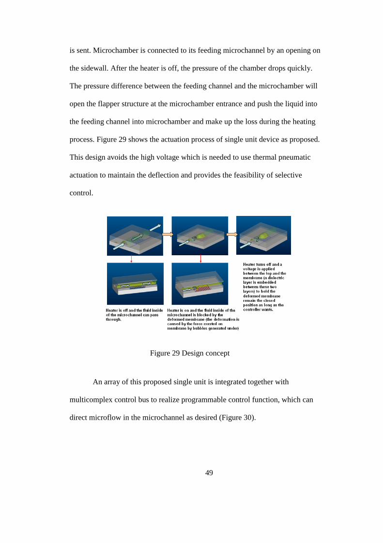
49
is sent. Microchamber is connected to its feeding microchannel by an opening on
the sidewall. After the heater is off, the pressure of the chamber drops quickly.
The pressure difference between the feeding channel and the microchamber will
open the flapper structure at the microchamber entrance and push the liquid into
the feeding channel into microchamber and make up the loss during the heating
process. Figure 29 shows the actuation process of single unit device as proposed.
This design avoids the high voltage which is needed to use thermal pneumatic
actuation to maintain the deflection and provides the feasibility of selective
control.
Figure 29 Design concept
An array of this proposed single unit is integrated together with
multicomplex control bus to realize programmable control function, which can
direct microflow in the microchannel as desired (Figure 30).
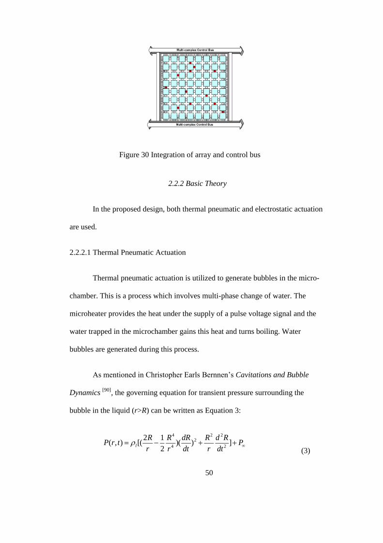
50
Figure 30 Integration of array and control bus
2.2.2 Basic Theory
In the proposed design, both thermal pneumatic and electrostatic actuation
are used.
2.2.2.1 Thermal Pneumatic Actuation
Thermal pneumatic actuation is utilized to generate bubbles in the micro-
chamber. This is a process which involves multi-phase change of water. The
microheater provides the heat under the supply of a pulse voltage signal and the
water trapped in the microchamber gains this heat and turns boiling. Water
bubbles are generated during this process.
As mentioned in Christopher Earls Bernnen’s Cavitations and Bubble
Dynamics [90]
, the governing equation for transient pressure surrounding the
bubble in the liquid (r>R) can be written as Equation 3:
Pdt
Rd
r
R
dt
dR
r
R
r
RtrP l ]))(
2
12[(),(
2
222
4
4
(3)

51
Where ρl is the constant liquid density, R is the radius of the bubble at time
t, r is the position vector and P∞ is the initial pressure of the liquid (Figure 31).
Figure 31 Semi-sphere bubble diagram
At the surface of the bubble, where the pressure is applied to the
membrane, the pressure is described as Equation 4:
PR
S
dt
dR
dt
RdRPb
2])(
2
3[ 2
2
2
(4)
At different time, the radius of the bubble follows Equation 5:
]2
1[2
Tk
tqt
L
TcbR b
v
l
(5)
Where b is a constant, α is the thermal diffusivity of the liquid and is a
function of liquid thermal conductivity k and liquid density ρl and specific heat of
the liquid c as in Equation 6:
c
k
l
(6)
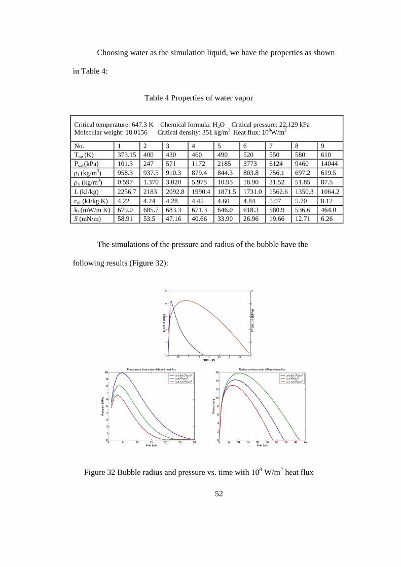
52
Choosing water as the simulation liquid, we have the properties as shown
in Table 4:
Table 4 Properties of water vapor
Critical temperature: 647.3 K Chemical formula: H2O Critical pressure: 22,129 kPa
Molecular weight: 18.0156 Critical density: 351 kg/m3 Heat flux: 10
8W/m
2
No. 1 2 3 4 5 6 7 8 9
Tsat (K) 373.15 400 430 460 490 520 550 580 610
Psat (kPa) 101.3 247 571 1172 2185 3773 6124 9460 14044
l (kg/m3) 958.3 937.5 910.3 879.4 844.3 803.8 756.1 697.2 619.5
v (kg/m3) 0.597 1.370 3.020 5.975 10.95 18.90 31.52 51.85 87.5
L (kJ/kg) 2256.7 2183 2092.8 1990.4 1871.5 1731.0 1562.6 1350.3 1064.2
cpl (kJ/kg K) 4.22 4.24 4.28 4.45 4.60 4.84 5.07 5.70 8.12
kl (mW/m K) 679.0 685.7 683.3 671.3 646.0 618.3 580.9 536.6 464.0
S (mN/m) 58.91 53.5 47.16 40.66 33.90 26.96 19.66 12.71 6.26
The simulations of the pressure and radius of the bubble have the
following results (Figure 32):
Figure 32 Bubble radius and pressure vs. time with 108 W/m
2 heat flux
53
When the heat flux is decreased down to 2x10⁷ W/m
2, though the diameter
of the bubble can reach approximately 150 µm theoretically, the pressure inside of
the bubble decreased dramatically to 0.2MPa. It is clear that when the heat flux is
smaller, the pressure get will be lower. However the time to reach the point where
the pressure is relatively high and the bubble is relatively large is longer.
When the bubble is formed, the pressure in the bubble is the vapor
pressure which can be simulated as the following method. The temperature Tv and
pressure Pv in the bubble are assumed to be uniform and are related by an integral
form of the equilibrium Calpeyron-Clausius equation
)11
(exp(vb
vap
atmvTTR
wQPP
(7)
And the equation of state for ideal gas:
v
v
v RTw
P
(8)
where the initial condition is,
KPaPatm 3.101 Kmol
JRc
3148.8
KTb 373
mol
kgw 3101
kg
JQvap
61026.2
54
The vapor inside of the bubbles is based on the law of ideal gas and when
the temperature is below the critical temperature, the higher the vapor temperature,
the higher pressure the vapor. So under the assumption that there is no mass
transport between the liquid and gas interface (where the bubble surface is), once
the bubble is deformed, if the temperature continues rising, the pressure will
exceed the original bubble pressure.
Figure 33 shows the change of the pressure with the temperature under 108
W/m2 heat flux.
Figure 33 Temperatures and pressures of Vapor in Bubbles
2.2.2.2 Electrostatic Actuation
Electrostatic actuation provides the force needed to maintain the deflection
of the PDMS membrane to close the microchannel. As designed, both the
membrane and inner surface of the microchannel have been treated to be electric
conductive and a dielectric material is coated to avoid short contact. The two
55
surfaces will act as a capacitor. To simplify the simulation, these two surfaces are
treated as two parallel plates since the dielectric layer is uniform along the surface,
and a parallel plate capacitor is used as simulation model. When a bias voltage is
applied, an electrostatic force will be produced. Since the lower metal plate is
fixed onto the substrate, the electrostatic force will act on the upper plate and
cause the deformation of the upper plate. We can deem the electrostatic force like
a spring force and the whole device can be modeled as shown in Figure 34.
Figure 34 Simplified Model of Parallel Metallic Electrodes
Electrostatic force in a parallel plate capacitor obeys the following basic
equations (Equation 7 and 8):
Q CV (9)
0 AC
g
(10)
Where g is the gap distance between the two plates and A is the overlap
area A wx (w is the width of the plate and x is the length). The energy stored
between these two plates under the voltage V is displayed in Equation 9.
56
2 201 1
2 2
AW CV V
g
(11)
Therefore the force is: 20
2
1
2
AWF V
x g
(12)
At equilibrium, electrostatic force is balanced by elastic force:
electrostatic elasticF F
20
2
1
2
AV kz
g
Where z is the biggest displacement (at equilibrium) of the upper plate and
the k is the spring constant of the membrane, which leads to Equation 11:
20
22
Az V
kg
(13)
At the same time, when electrostatic force is applied to the upper metal
plate, which is covered by a layer of PDMS, the deformation caused by the
electrostatic force is expressed as Equation 12:
Ftt
AE
(14)
If the PDMS membrane with electrodes is around 20 μm thick and the
dielectric constant layer uses 2 μm thick parylene, the voltage needed between the
two electrodes will satisfy Equation 13:
57
4
0
23
max
0138.015.3
2
a
dhEwVneed
(15)
Where wmax is the maximum deflection of the PDMS membrane and
wmax=50 μm and equals to the radius of the proposed microchannel, E is Young’s
modulus of PDMS membrane, h is the thickness of the membrane, d is the gap
caused by the dielectric layer which is the thickness of parylene layer and a is the
side length of the square membrane which is 200 μm. Using these values in, the
voltage needed applied to the two electrodes to hold a 50 μm deflection of a
PDMS membrane is 50V.
2.2.2.3 Conclusion
As mentioned, the governing equation for transient pressure surrounding
the bubble in the liquid (r>R) is Pdt
Rd
r
R
dt
dR
r
R
r
RtrP l ]))(
2
12[(),(
2
222
4
4
.
Simultaneously, the radius change of the bubble versus time follows (Equation 5)
]2
1[2
Tk
tqt
L
TcbR b
v
l
. The simulation result shows that when the heat
flux is smaller, the pressure get will be smaller but the time to reach the point
where the pressure is relatively high and the bubble is relatively large is longer.
The heat flux can be located at a value of 5~8 x 10⁷ W/m
2 to get a better actuation.
Figure 32 shows that the pressure drops down to normal in about 4 μsec, which
means that if the pressure is used as an actuation force, only the early time of the
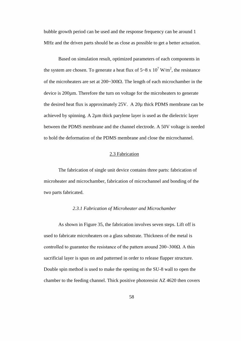
58
bubble growth period can be used and the response frequency can be around 1
MHz and the driven parts should be as close as possible to get a better actuation.
Based on simulation result, optimized parameters of each components in
the system are chosen. To generate a heat flux of 5~8 x 10⁷ W/m
2, the resistance
of the microheaters are set at 200~300. The length of each microchamber in the
device is 200µm. Therefore the turn on voltage for the microheaters to generate
the desired heat flux is approximately 25V. A 20µ thick PDMS membrane can be
achieved by spinning. A 2µm thick parylene layer is used as the dielectric layer
between the PDMS membrane and the channel electrode. A 50V voltage is needed
to hold the deformation of the PDMS membrane and close the microchannel.
2.3 Fabrication
The fabrication of single unit device contains three parts: fabrication of
microheater and microchamber, fabrication of microchannel and bonding of the
two parts fabricated.
2.3.1 Fabrication of Microheater and Microchamber
As shown in Figure 35, the fabrication involves seven steps. Lift off is
used to fabricate microheaters on a glass substrate. Thickness of the metal is
controlled to guarantee the resistance of the pattern around 200~300Ω. A thin
sacrificial layer is spun on and patterned in order to release flapper structure.
Double spin method is used to make the opening on the SU-8 wall to open the
chamber to the feeding channel. Thick positive photoresist AZ 4620 then covers
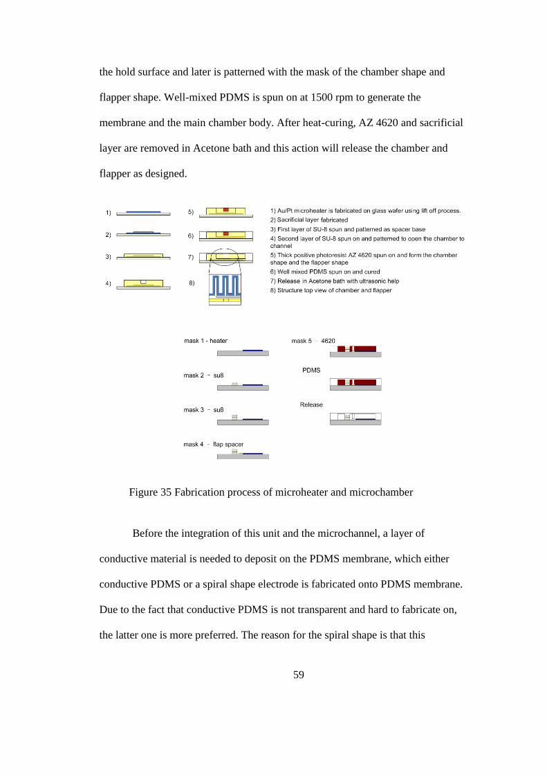
59
the hold surface and later is patterned with the mask of the chamber shape and
flapper shape. Well-mixed PDMS is spun on at 1500 rpm to generate the
membrane and the main chamber body. After heat-curing, AZ 4620 and sacrificial
layer are removed in Acetone bath and this action will release the chamber and
flapper as designed.
Figure 35 Fabrication process of microheater and microchamber
Before the integration of this unit and the microchannel, a layer of
conductive material is needed to deposit on the PDMS membrane, which either
conductive PDMS or a spiral shape electrode is fabricated onto PDMS membrane.
Due to the fact that conductive PDMS is not transparent and hard to fabricate on,
the latter one is more preferred. The reason for the spiral shape is that this
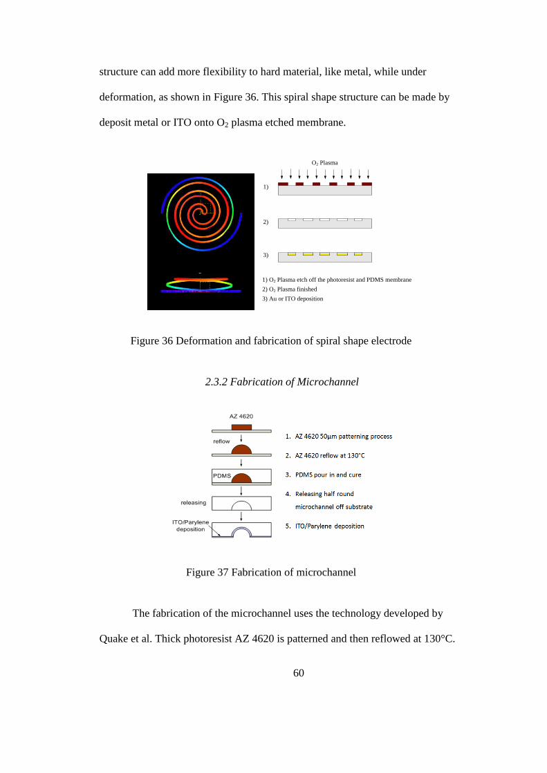
60
structure can add more flexibility to hard material, like metal, while under
deformation, as shown in Figure 36. This spiral shape structure can be made by
deposit metal or ITO onto O2 plasma etched membrane.
O2 Plasma
1)
2)
3)
1) O2 Plasma etch off the photoresist and PDMS membrane
2) O2 Plasma finished
3) Au or ITO deposition
Figure 36 Deformation and fabrication of spiral shape electrode
2.3.2 Fabrication of Microchannel
Figure 37 Fabrication of microchannel
The fabrication of the microchannel uses the technology developed by
Quake et al. Thick photoresist AZ 4620 is patterned and then reflowed at 130°C.

61
Reflowed photoresist will hold its round shape due to the surface tension effect of
liquid and after cooling down. The round shape can then be transferred to the
PDMS as shown in Figure 37. In order to make the inner surface of the channel to
be conductive, a thin layer of ITO is deposited on to it. A 2 µm thick parylene film
is then used to cover this conductive area in order to avoid short contact with the
conductive material on top of the membrane.
2.3.3 Bonding between Microchamber and Microchannel
Because the bonding surfaces of two parts are all PDMS, two methods are
performed to bond them together.
The first method is used in conventional fabrication of PDMS. Both
PDMS surfaces are treated under O2 Plasma for about 20~30 seconds and then
forcibly pressed together for about 2 hours for full bonding. The oxygen plasma
introduces hydroxyl groups on the surface of the materials that are used to make
them bond irreversibly to each other.
The second method is developed by Quake’s group. They utilized the
feature that different mixing ratio can result in different properties of PDMS to
realize bonding between two parts that contain different exceeding components.
The two parts can be bonded together into one part under heat. By choosing the
microchannel to be base-over part and the PDMS membrane to be crosslinker-
over part and re-curing them together, the proposed structure can be easily
realized.
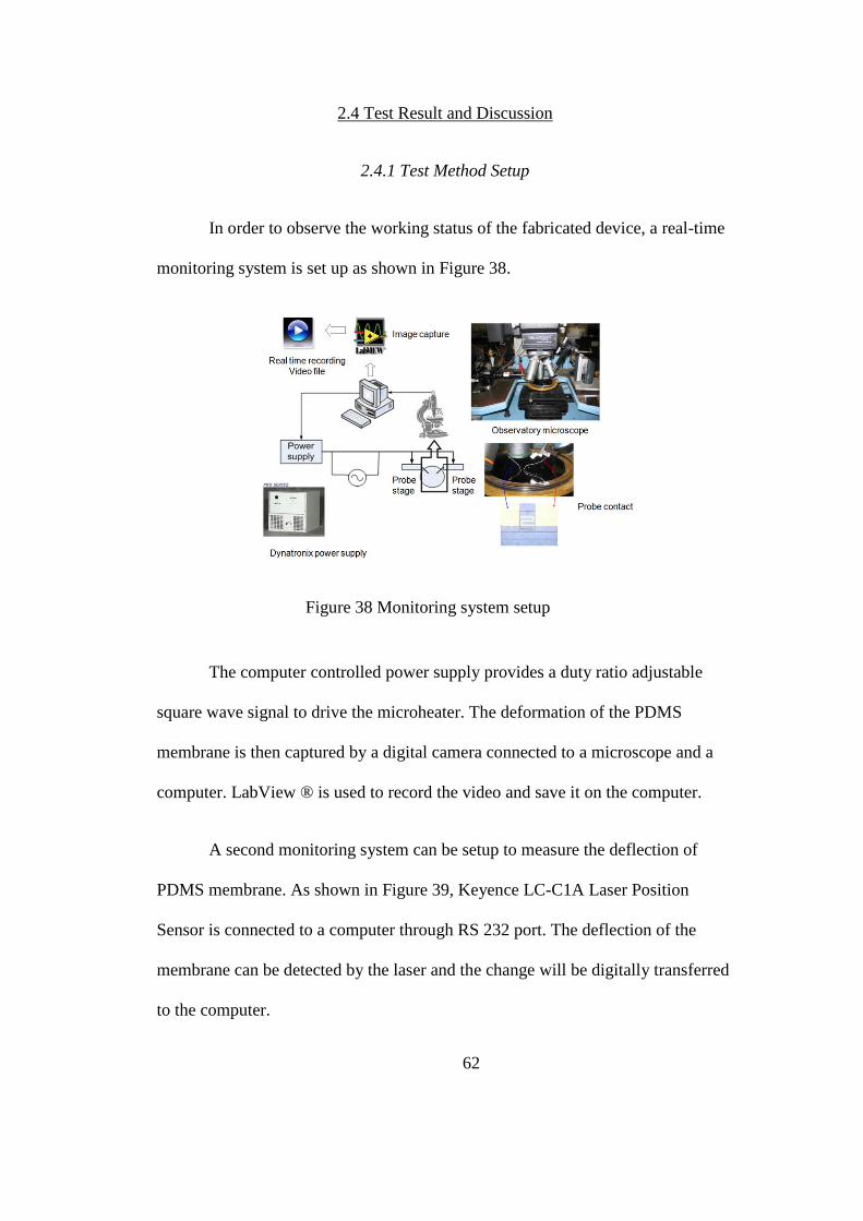
62
2.4 Test Result and Discussion
2.4.1 Test Method Setup
In order to observe the working status of the fabricated device, a real-time
monitoring system is set up as shown in Figure 38.
Figure 38 Monitoring system setup
The computer controlled power supply provides a duty ratio adjustable
square wave signal to drive the microheater. The deformation of the PDMS
membrane is then captured by a digital camera connected to a microscope and a
computer. LabView ® is used to record the video and save it on the computer.
A second monitoring system can be setup to measure the deflection of
PDMS membrane. As shown in Figure 39, Keyence LC-C1A Laser Position
Sensor is connected to a computer through RS 232 port. The deflection of the
membrane can be detected by the laser and the change will be digitally transferred
to the computer.
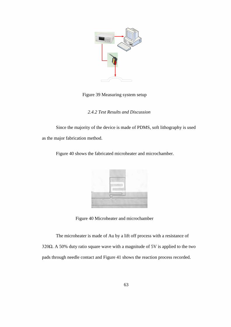
63
Figure 39 Measuring system setup
2.4.2 Test Results and Discussion
Since the majority of the device is made of PDMS, soft lithography is used
as the major fabrication method.
Figure 40 shows the fabricated microheater and microchamber.
Figure 40 Microheater and microchamber
The microheater is made of Au by a lift off process with a resistance of
320Ω. A 50% duty ratio square wave with a magnitude of 5V is applied to the two
pads through needle contact and Figure 41 shows the reaction process recorded.
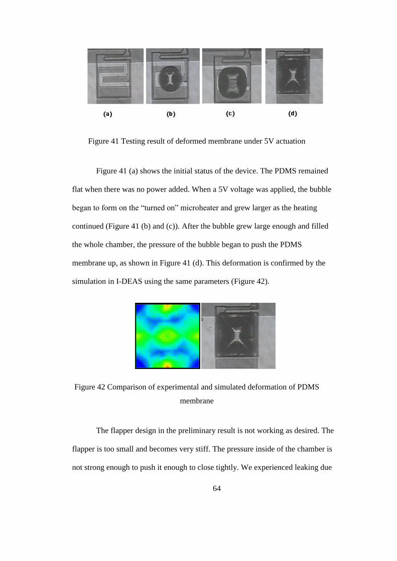
64
Figure 41 Testing result of deformed membrane under 5V actuation
Figure 41 (a) shows the initial status of the device. The PDMS remained
flat when there was no power added. When a 5V voltage was applied, the bubble
began to form on the “turned on” microheater and grew larger as the heating
continued (Figure 41 (b) and (c)). After the bubble grew large enough and filled
the whole chamber, the pressure of the bubble began to push the PDMS
membrane up, as shown in Figure 41 (d). This deformation is confirmed by the
simulation in I-DEAS using the same parameters (Figure 42).
Figure 42 Comparison of experimental and simulated deformation of PDMS
membrane
The flapper design in the preliminary result is not working as desired. The
flapper is too small and becomes very stiff. The pressure inside of the chamber is
not strong enough to push it enough to close tightly. We experienced leaking due
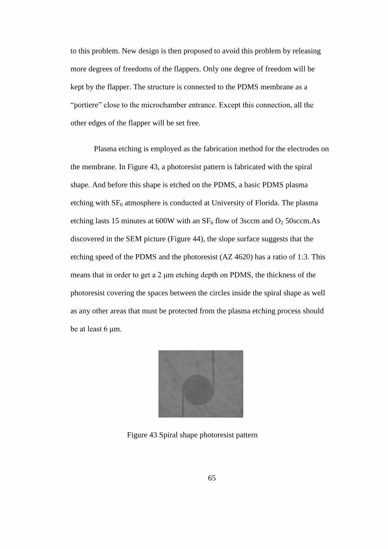
65
to this problem. New design is then proposed to avoid this problem by releasing
more degrees of freedoms of the flappers. Only one degree of freedom will be
kept by the flapper. The structure is connected to the PDMS membrane as a
“portiere” close to the microchamber entrance. Except this connection, all the
other edges of the flapper will be set free.
Plasma etching is employed as the fabrication method for the electrodes on
the membrane. In Figure 43, a photoresist pattern is fabricated with the spiral
shape. And before this shape is etched on the PDMS, a basic PDMS plasma
etching with SF6 atmosphere is conducted at University of Florida. The plasma
etching lasts 15 minutes at 600W with an SF6 flow of 3sccm and O2 50sccm.As
discovered in the SEM picture (Figure 44), the slope surface suggests that the
etching speed of the PDMS and the photoresist (AZ 4620) has a ratio of 1:3. This
means that in order to get a 2 μm etching depth on PDMS, the thickness of the
photoresist covering the spaces between the circles inside the spiral shape as well
as any other areas that must be protected from the plasma etching process should
be at least 6 μm.
Figure 43 Spiral shape photoresist pattern
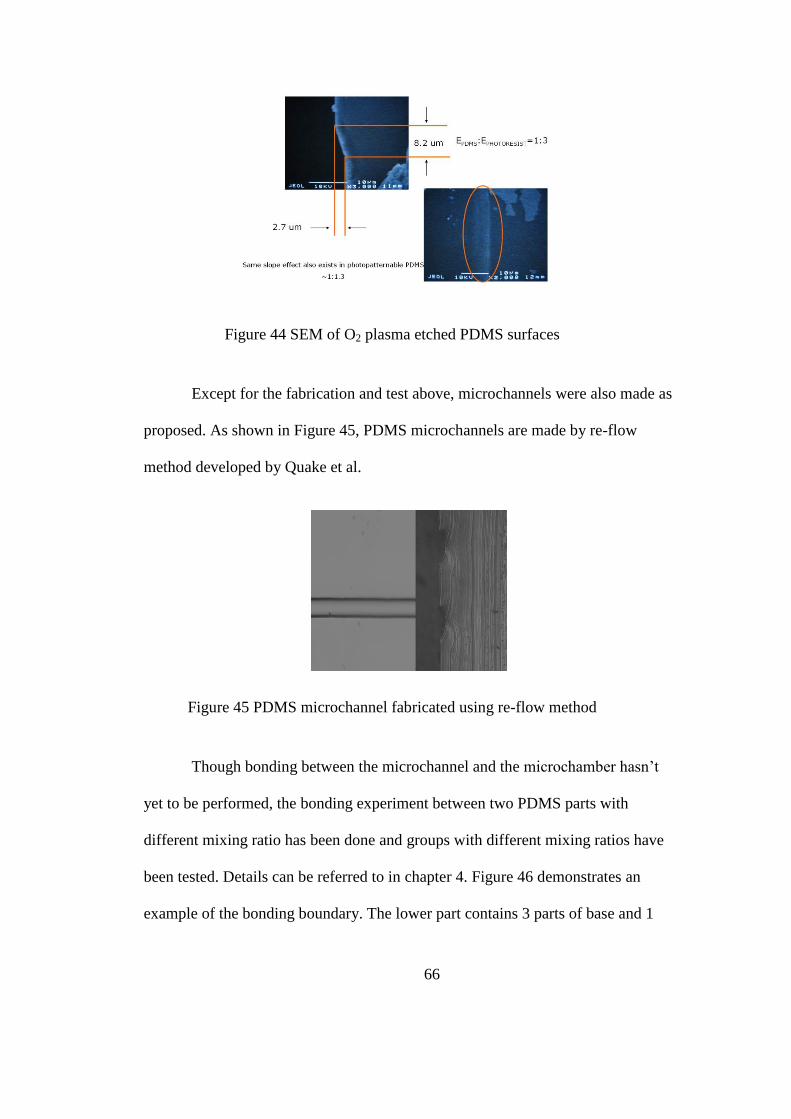
66
Figure 44 SEM of O2 plasma etched PDMS surfaces
Except for the fabrication and test above, microchannels were also made as
proposed. As shown in Figure 45, PDMS microchannels are made by re-flow
method developed by Quake et al.
Figure 45 PDMS microchannel fabricated using re-flow method
Though bonding between the microchannel and the microchamber hasn’t
yet to be performed, the bonding experiment between two PDMS parts with
different mixing ratio has been done and groups with different mixing ratios have
been tested. Details can be referred to in chapter 4. Figure 46 demonstrates an
example of the bonding boundary. The lower part contains 3 parts of base and 1
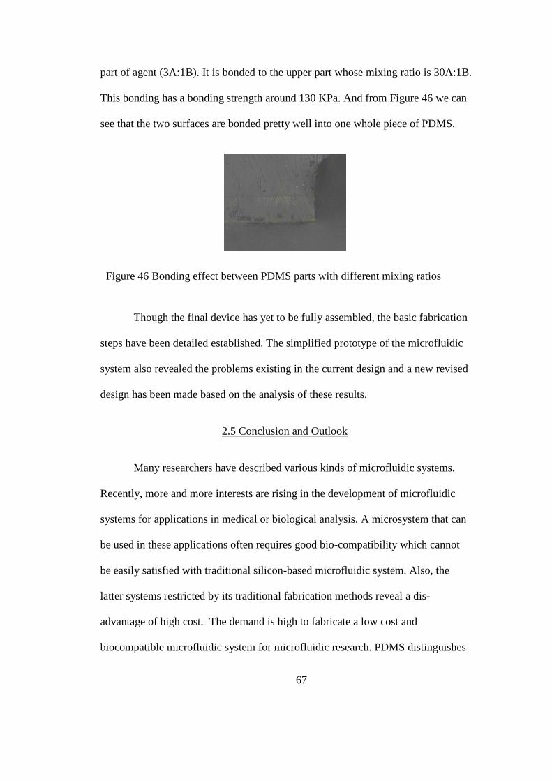
67
part of agent (3A:1B). It is bonded to the upper part whose mixing ratio is 30A:1B.
This bonding has a bonding strength around 130 KPa. And from Figure 46 we can
see that the two surfaces are bonded pretty well into one whole piece of PDMS.
Figure 46 Bonding effect between PDMS parts with different mixing ratios
Though the final device has yet to be fully assembled, the basic fabrication
steps have been detailed established. The simplified prototype of the microfluidic
system also revealed the problems existing in the current design and a new revised
design has been made based on the analysis of these results.
2.5 Conclusion and Outlook
Many researchers have described various kinds of microfluidic systems.
Recently, more and more interests are rising in the development of microfluidic
systems for applications in medical or biological analysis. A microsystem that can
be used in these applications often requires good bio-compatibility which cannot
be easily satisfied with traditional silicon-based microfluidic system. Also, the
latter systems restricted by its traditional fabrication methods reveal a dis-
advantage of high cost. The demand is high to fabricate a low cost and
biocompatible microfluidic system for microfluidic research. PDMS distinguishes
68
itself from other MEMS materials by its great elastomeric properties and
simplicity in fabrication, low-cost and good biocompatibility. Soft lithography
enables the expanding of PDMS-based microfluidic systems’ application field and
brings more and more multidisciplinary integrations as a total analysis system.
In the work of this chapter, a PDMS-based customer programmable
microfluidic system has been developed. A prototype of the system is tested with
a 5V voltage for actuation. Soft lithography is employed in the fabrication process
for this microfluidic system. Thick positive photoresist AZ 4620 was used as a
sacrificial layer to form the reaction chamber. Different ratio PDMS bonding was
tested with the consideration of final integration of the system.
This microfluidic system provides a universal platform for different
application of microfluidic systems where microflow control is needed, whether it
is used in chemical or biological analysis. The major components of the system
are made from PDMS which assures the good biocompatibility of the whole
system. The applications for this microfluidic system are not restricted to micro-
fluidics only. The good deformability of the PDMS membrane in the system
provides even more possibility for it to be adopted into other applications such as
micromirror arrays.
The developed systems showed a noticeable deformation of the PDMS
membrane. Yet the characterization of this deformability of PDMS needs further
study into the mechanical behavior at a microscale which is discussed in the
following chapter.
69
CHAPTER 3 MICROMIRROR ARRAYS
3.1 Introduction
The ideal of deformable micromirror was first proposed in 1986 [63]
with a
layer of deformable viscoelastic reflective material with electrostatically driven.
Through the efforts of the past few years, several types of high performance
deformable micromirror have been developed. Most of the micromirrors usually
are voltage-driven and provide the potential of integration with independent pixel
control through different control circuits. However, with the use of traditional
microfabrication, these families of micromirror are limited from most applications
because of their prohibitively high cost introduced by the fabrication of
complicated structures. At the same time, even though these actuation methods are
well developed; limitations in performance, size and complexity in their
manufacturing restrain their practical applications. The flexibility of fabrication
and integration of polymer materials especially PDMS which is optically
transparent at a wide range of wavelengths has significantly reduced the cost of
the mirrors and combined with the advantage brought by MEMS technology. It
has been used to form lenses[91, 92]
and waveguides[93, 94]
.
Deformable micromirrors provide a low-cost adaptive optics solution
which holds the promise of a low power compact high performance. With large
mirror deflection achieved, it can be used in applications from sophisticated
optical cross-connects[95]
to human retina imagining[66]
, extending the field from
70
astronomical imaging systems[96]
to laser-based communication[97]
and biomedical
imaging[66, 98, 99]
.
3.2 Design and Simulation
Inspired by the design of the programmable microfluidic system discussed
in the previous chapter, we inherit the system’s design and adjust it for fabricating
micromirror arrays for adaptive optics. A thin layer of metal is patterned into
micromirror arrays to reflect the incoming light. The mirror arrays are then
transferred to the PDMS membrane. This membrane is deformed by the
microheaters, which are integrated in the PDMS chamber under the membrane.
The arrays embedded in the PDMS membrane inherit the deformation of the
membrane and form a deformed reflection surface. The deformability is precisely
controlled by adjusting the voltage applied on the microheaters. Since the
microheaters are addressed with multi-complex control bus, the deformation of
the whole mirror surface can be adjusted based on needs. Based on the discussion
in Chapter 2, this thermal-pneumatically driven scheme provides a significant
benefit in achieving large stroke deformations. State-of-the-art electrostatically
driven mirror can provide only 8 µm of stroke with very high voltage while the
proposed micromirrors can easily reach up to 10 µm with less voltage.
Multiple arrays were designed with different lengths (16 µm, 32µm, 64
µm, 128 µm and 256 µm). Each different length design is arrayed into several
array sizes. Demonstrated in
Figure 47 is a 14×14 array with a dimension of 64µm×64µm.
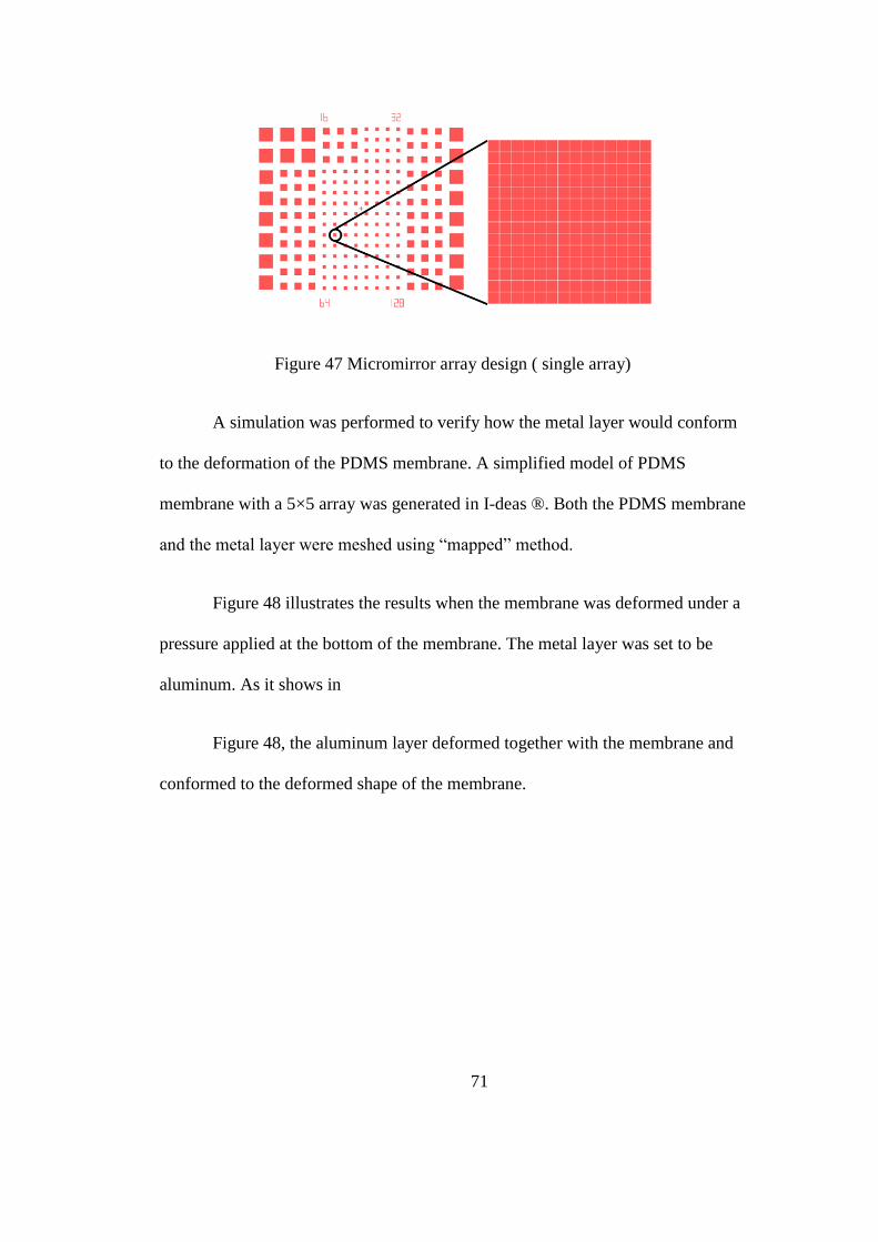
71
Figure 47 Micromirror array design ( single array)
A simulation was performed to verify how the metal layer would conform
to the deformation of the PDMS membrane. A simplified model of PDMS
membrane with a 5×5 array was generated in I-deas ®. Both the PDMS membrane
and the metal layer were meshed using “mapped” method.
Figure 48 illustrates the results when the membrane was deformed under a
pressure applied at the bottom of the membrane. The metal layer was set to be
aluminum. As it shows in
Figure 48, the aluminum layer deformed together with the membrane and
conformed to the deformed shape of the membrane.
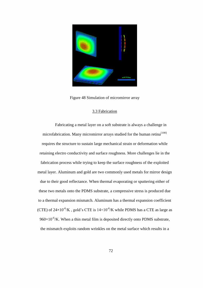
72
Figure 48 Simulation of micromirror array
3.3 Fabrication
Fabricating a metal layer on a soft substrate is always a challenge in
microfabrication. Many micromirror arrays studied for the human retina[100]
requires the structure to sustain large mechanical strain or deformation while
retaining electro conductivity and surface roughness. More challenges lie in the
fabrication process while trying to keep the surface roughness of the exploited
metal layer. Aluminum and gold are two commonly used metals for mirror design
due to their good reflectance. When thermal evaporating or sputtering either of
these two metals onto the PDMS substrate, a compressive stress is produced due
to a thermal expansion mismatch. Aluminum has a thermal expansion coefficient
(CTE) of 24×10-6
/K , gold’s CTE is 14×10-6
/K while PDMS has a CTE as large as
960×10-6
/K. When a thin metal film is deposited directly onto PDMS substrate,
the mismatch exploits random wrinkles on the metal surface which results in a
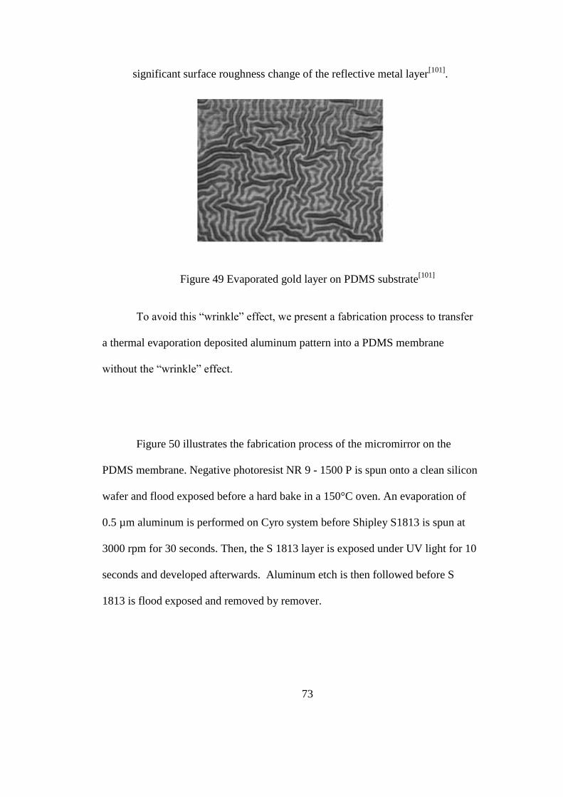
73
significant surface roughness change of the reflective metal layer[101]
.
Figure 49 Evaporated gold layer on PDMS substrate[101]
To avoid this “wrinkle” effect, we present a fabrication process to transfer
a thermal evaporation deposited aluminum pattern into a PDMS membrane
without the “wrinkle” effect.
Figure 50 illustrates the fabrication process of the micromirror on the
PDMS membrane. Negative photoresist NR 9 - 1500 P is spun onto a clean silicon
wafer and flood exposed before a hard bake in a 150°C oven. An evaporation of
0.5 µm aluminum is performed on Cyro system before Shipley S1813 is spun at
3000 rpm for 30 seconds. Then, the S 1813 layer is exposed under UV light for 10
seconds and developed afterwards. Aluminum etch is then followed before S
1813 is flood exposed and removed by remover.
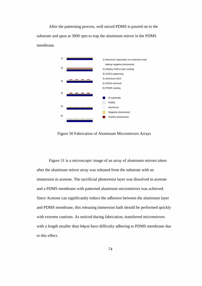
74
After the patterning process, well mixed PDMS is poured on to the
substrate and spun at 3000 rpm to trap the aluminum mirror in the PDMS
membrane.
Aluminum
Negative photoresist
Positive photoresist
Si substrate
PDMS
1)
2)
3)
4)
5)
6)
1) Aluminum deposition on extensive hard
baking negative photoresist.
2) Shipley S1813 spin coating
3) S1813 patterning
4) Aluminum Etch
5) S1813 removal
6) PDMS coating
Figure 50 Fabrication of Aluminum Micromirrors Arrays
Figure 51 is a microscopic image of an array of aluminum mirrors taken
after the aluminum mirror array was released from the substrate with an
immersion in acetone. The sacrificial photoresist layer was dissolved in acetone
and a PDMS membrane with patterned aluminum micromirrors was achieved.
Since Acetone can significantly reduce the adhesion between the aluminum layer
and PDMS membrane, this releasing immersion bath should be performed quickly
with extreme cautions. As noticed during fabrication, transferred micromirrors
with a length smaller than 64µm have difficulty adhering to PDMS membrane due
to this effect.
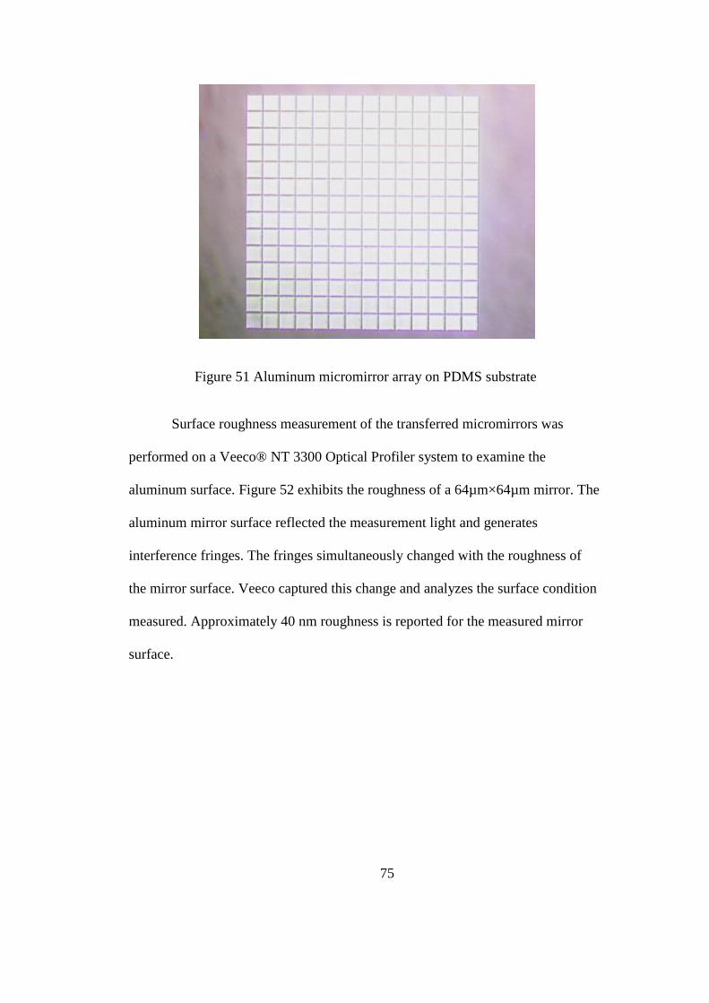
75
Figure 51 Aluminum micromirror array on PDMS substrate
Surface roughness measurement of the transferred micromirrors was
performed on a Veeco® NT 3300 Optical Profiler system to examine the
aluminum surface. Figure 52 exhibits the roughness of a 64µm×64µm mirror. The
aluminum mirror surface reflected the measurement light and generates
interference fringes. The fringes simultaneously changed with the roughness of
the mirror surface. Veeco captured this change and analyzes the surface condition
measured. Approximately 40 nm roughness is reported for the measured mirror
surface.
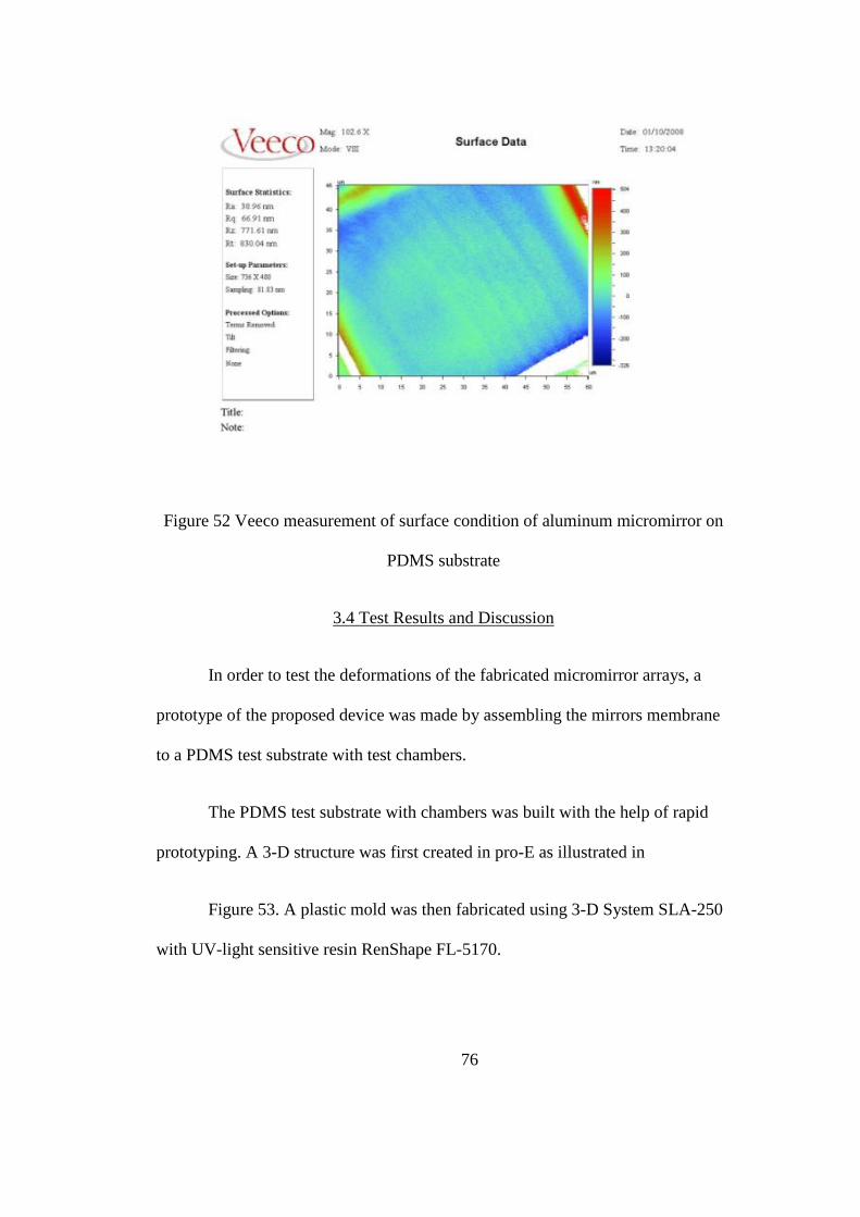
76
Figure 52 Veeco measurement of surface condition of aluminum micromirror on
PDMS substrate
3.4 Test Results and Discussion
In order to test the deformations of the fabricated micromirror arrays, a
prototype of the proposed device was made by assembling the mirrors membrane
to a PDMS test substrate with test chambers.
The PDMS test substrate with chambers was built with the help of rapid
prototyping. A 3-D structure was first created in pro-E as illustrated in
Figure 53. A plastic mold was then fabricated using 3-D System SLA-250
with UV-light sensitive resin RenShape FL-5170.
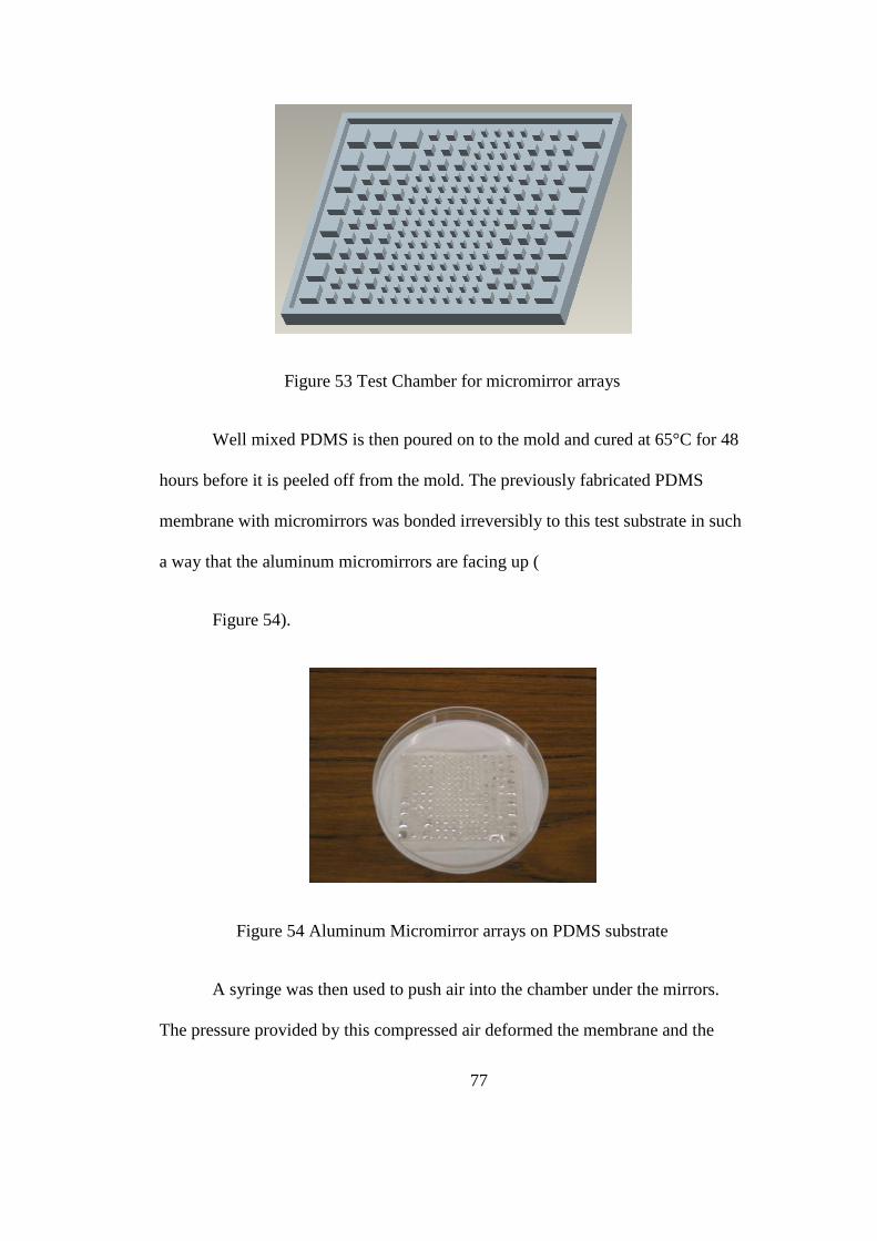
77
Figure 53 Test Chamber for micromirror arrays
Well mixed PDMS is then poured on to the mold and cured at 65°C for 48
hours before it is peeled off from the mold. The previously fabricated PDMS
membrane with micromirrors was bonded irreversibly to this test substrate in such
a way that the aluminum micromirrors are facing up (
Figure 54).
Figure 54 Aluminum Micromirror arrays on PDMS substrate
A syringe was then used to push air into the chamber under the mirrors.
The pressure provided by this compressed air deformed the membrane and the
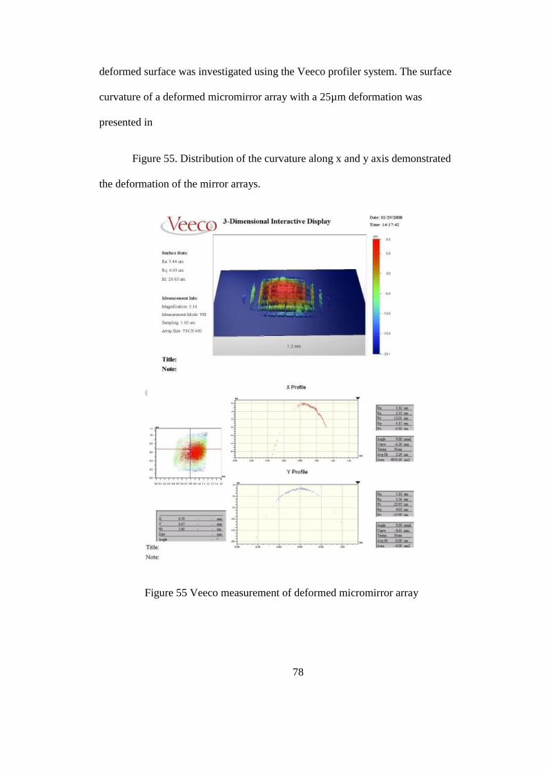
78
deformed surface was investigated using the Veeco profiler system. The surface
curvature of a deformed micromirror array with a 25µm deformation was
presented in
Figure 55. Distribution of the curvature along x and y axis demonstrated
the deformation of the mirror arrays.
Figure 55 Veeco measurement of deformed micromirror array
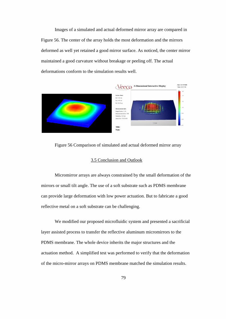
79
Images of a simulated and actual deformed mirror array are compared in
Figure 56. The center of the array holds the most deformation and the mirrors
deformed as well yet retained a good mirror surface. As noticed, the center mirror
maintained a good curvature without breakage or peeling off. The actual
deformations conform to the simulation results well.
Figure 56 Comparison of simulated and actual deformed mirror array
3.5 Conclusion and Outlook
Micromirror arrays are always constrained by the small deformation of the
mirrors or small tilt angle. The use of a soft substrate such as PDMS membrane
can provide large deformation with low power actuation. But to fabricate a good
reflective metal on a soft substrate can be challenging.
We modified our proposed microfluidic system and presented a sacrificial
layer assisted process to transfer the reflective aluminum micromirrors to the
PDMS membrane. The whole device inherits the major structures and the
actuation method. A simplified test was performed to verify that the deformation
of the micro-mirror arrays on PDMS membrane matched the simulation results.
80
The surface profile was studied with the aid of a Veeco profile system. The
deformed micromirror arrays maintained a good curvature without breakage or
peeling off.
Further characterization of this deformable micromirror array will be able
to reveal the detailed relationship between the driven power and the reflection
ability. Also, an improved structure or a primer coating process to improve and
secure the adhesion of reflective surfaces to PDMS membrane in large
deformation scenario is foreseeable by the current result.
The developed micromirror system provides a cost-effective solution to
those applications from sophisticated optical cross-connects to human retina
imagining with its unique deformability.
81
CHAPTER 4 MECHANICAL PROPERTIES OF PDMS
4.1 Introduction
Recent developments in MEMS technology are generating new
opportunities for applications in biological and medical analysis. The diversity of
these applications has encouraged new fabrication technologies and new materials
to be revealed. The practical nature of polymers along with rapid prototyping and
mass production as well as lower cost compared with silicon make them uniquely
qualified for the development of BioMEMS.
Much like other MEMS materials used in a wide variety of applications,
polymer structures also suffer from degradation or failure mechanisms. In fact, the
properties of all the materials in thin film technology are often different from the
macro scale bulk behavior. Nowadays, the macro-scale bulk material properties of
MEMS materials are often used as micro-scale properties by assumption, which
produces unreliable results in MEMS design and simulation. As a result of scaling
laws, materials behave stiffer or stronger as the sample size decreases. This means
a material which is soft in bulk volume might act like a hard material when its
application size is scaled down. Therefore, micro mechanical test on MEMS
materials is necessary when studying the mechanical behaviors of materials on the
micro-scale.
Among the polymers used to fabricate microfluidic systems, like
polyurethane, polyimide, polycarbonate, polymethylmethacrylate (PMMA),

82
polystyrene, polyethyleneterephthalate glycol (PETG) and polyethylene,
Polydimethylsiloxane (PDMS) is the most widely used polymer in both academic
and industrial research groups for applications in microfluidics. With desirable
properties such as low cost, ease of mass production, microfabrication compatible,
high deformability and transparency, PDMS is a formidable and promising
material in MEMS. There is a significant need to examine this material’s
mechanical properties at both macro and micro scales with its application in
MEMS.
PDMS is a heat curable polymer which always comes in a two-part kit
consisting of a pre-polymer (also called base or part A) component and a cross-
linker (also called curing agent or part B) component. Although PDMS is
commonly mixed with a weight ratio 10A:1B, other ratios are also being used to
fabricate 3-D MEMS structures by bonding PDMS parts with different mixing
ratio. The mechanical properties of the cured PDMS vary with different mixing
ratios and may affect the function of designed devices. At the same time, the
bonding strength between these bonded PDMS parts is neither well-known nor
studied.
The use of PDMS in BioMEMS applications is promoted by the
development of Soft Lithography techniques including micromolding, micro
contact printing, replica molding, microtransfer molding, and solvent-assisted
micromolding. All these techniques usually involve photolithography to create a
mold before transferring micron or even submicron features to PDMS. During the
83
process, PDMS is either exposed or immersed into different chemicals such as
photoresist developers, organic solutions and acids. When PDMS is fabricated
into embedded structures in a microfluidic system, this polymer material may
sustain more than one kind of chemical liquid during the microfabrication process.
In addition to this, microfluidic systems which are made out of PDMS are often
used in bio-MEMS and serve as platforms for bio-reactions, such as in a Lab-on-
chip or in a PCR process [16, 77, 79, 102-104]
, long periods of contact with different bio-
chemicals are required.
Though PDMS stands out with its inner properties when used as a bulk
material, small changes can be observed after experiencing the chemical
immersion [105]
. The study of the mechanical property change of PDMS after
chemical immersion will benefit those researchers who utilize PDMS as a MEMS
material and make micro-scale PDMS devices. With the microfluidic systems
being used widely in bioMEMS, it is important to know how the PDMS will react
in these systems at a micro-scale in order to provide correct or precise information
in the results, both from a chemical aspect or mechanical aspect. Therefore, a
thorough mechanical property study of PDMS will be important for improving the
performance and durability of the MEMS devices.
Several studies have been conducted to reveal PDMS properties when it is
being used in a MEMS structures. Hwa Seng Khoo1, et al performed a mechanical
characterization of microscale elastomeric membrane by applying a central point
load [106]
. Some of the effects involved with chemical immersions were studied by
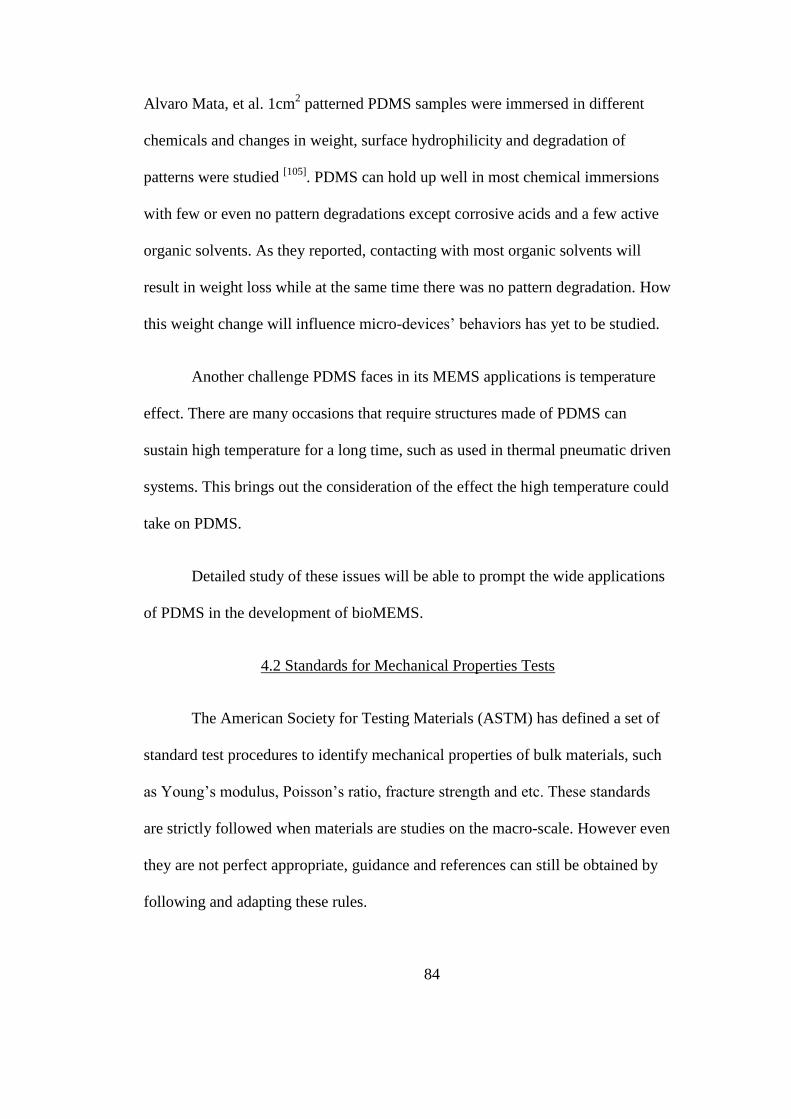
84
Alvaro Mata, et al. 1cm2 patterned PDMS samples were immersed in different
chemicals and changes in weight, surface hydrophilicity and degradation of
patterns were studied [105]
. PDMS can hold up well in most chemical immersions
with few or even no pattern degradations except corrosive acids and a few active
organic solvents. As they reported, contacting with most organic solvents will
result in weight loss while at the same time there was no pattern degradation. How
this weight change will influence micro-devices’ behaviors has yet to be studied.
Another challenge PDMS faces in its MEMS applications is temperature
effect. There are many occasions that require structures made of PDMS can
sustain high temperature for a long time, such as used in thermal pneumatic driven
systems. This brings out the consideration of the effect the high temperature could
take on PDMS.
Detailed study of these issues will be able to prompt the wide applications
of PDMS in the development of bioMEMS.
4.2 Standards for Mechanical Properties Tests
The American Society for Testing Materials (ASTM) has defined a set of
standard test procedures to identify mechanical properties of bulk materials, such
as Young’s modulus, Poisson’s ratio, fracture strength and etc. These standards
are strictly followed when materials are studies on the macro-scale. However even
they are not perfect appropriate, guidance and references can still be obtained by
following and adapting these rules.
85
There are two major categories for materials properties testing: direct
methods and inverse methods. Direct methods include the most commonly used
tensile test, which is also adapted by ASTM standards. Membranes test, resonant
test, bending test and other similar tests are grouped as inverse methods which a
model is constructed for the test structure. Both groups of tests are used to study
materials on the microscale by researchers.
4.2.1 Tensile Test
Many of the mechanical properties of a material can be extracted from a
tensile test. In a tensile test, a sample is strained at a constant rate and the stress
needed to maintain this strain rate is measured. The stress and strain can either be
measured in terms of engineering stress and strain or true stress and strain. The
elastic modulus, the ultimate tensile stress, the fracture stress, the modulus of
toughness, and the modulus of resilience can all be determined from a tensile test.
Figure 57 shows the test configuration. The specimen is fixed to a grip at
one end and held firmly while the other end is fixed to another grip which is
moving at a constant rate. Attached to the fixed grip, a force/displacement
transducer is glued using adhesive or connected with a pin and ring mechanism to
sense the elongation of the attached specimen.
86
Figure 57 Tensile test configurations
The stress of the specimen can be obtained using Equation 15
A
F (16)
And the strain of the specimen is defined as Equation 16
0L
L (17)
The Young’s modulus is then deduced from General Hook’s Law as
Equation 17
L
L
A
FE
0
(18)
A tensile test stands out from other tests because of its simplicity. Yet the
test requires extra attention when handling and mounting the specimen, especially
in the case of brittle materials. And microscale materials can be more difficult
than bulk materials.
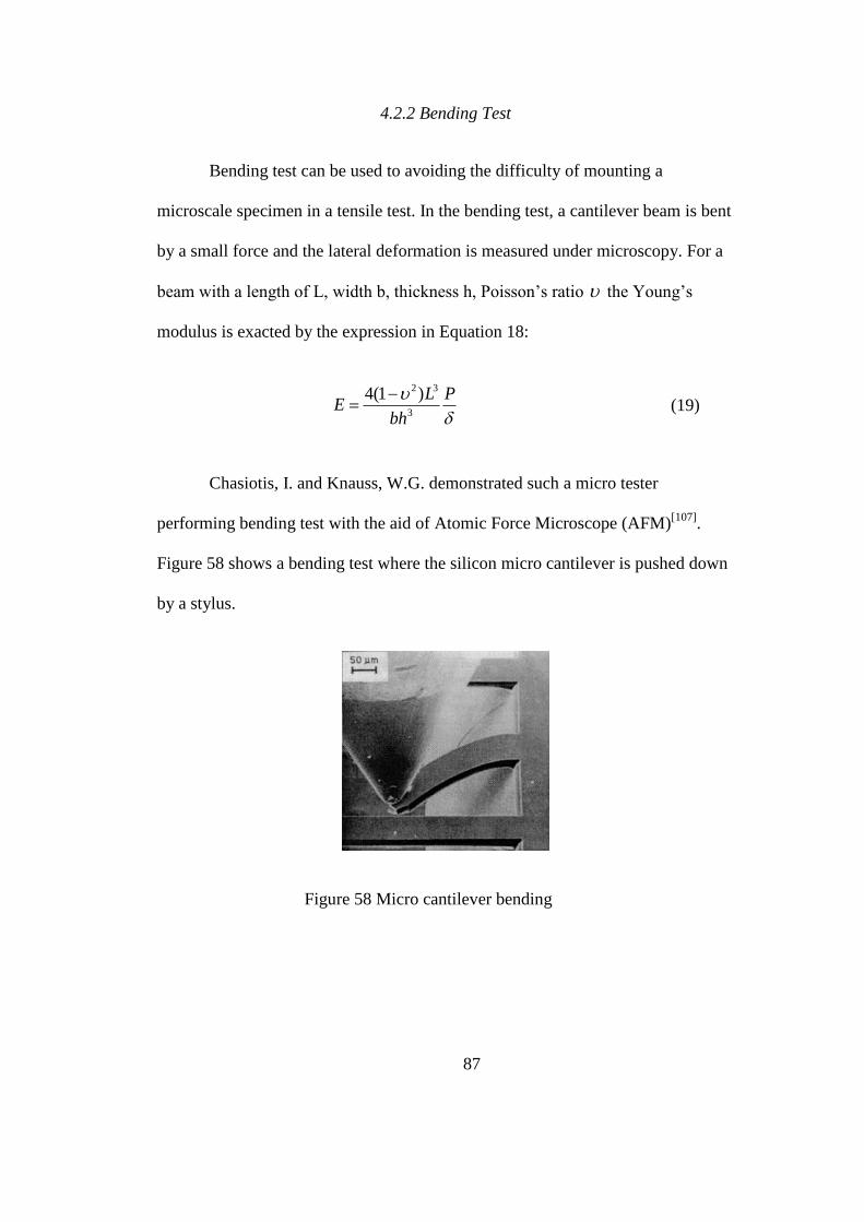
87
4.2.2 Bending Test
Bending test can be used to avoiding the difficulty of mounting a
microscale specimen in a tensile test. In the bending test, a cantilever beam is bent
by a small force and the lateral deformation is measured under microscopy. For a
beam with a length of L, width b, thickness h, Poisson’s ratio the Young’s
modulus is exacted by the expression in Equation 18:
P
bh
LE
3
32)1(4 (19)
Chasiotis, I. and Knauss, W.G. demonstrated such a micro tester
performing bending test with the aid of Atomic Force Microscope (AFM)[107]
.
Figure 58 shows a bending test where the silicon micro cantilever is pushed down
by a stylus.
Figure 58 Micro cantilever bending
88
4.2.3 Resonant Test
For an isotropic elastic cantilever beam, the following differential equation
(Equation 19) describes its free bending vibration with no damping:
02
2
4
4
x
yA
x
yEI (20)
Where y is the deflection of the beam, E is the Young’s modulus, I is the
inertia, is the density of the material and A is the area of cross-section of the
beam.
Based on the boundary condition of the cantilever beam, we can derive
from this equation that the 1st order frequency of the beam’s vibration with no
damping has the following relation with Young’s modulus (Equation 20):
//162.0 2 EIhfi (21)
When the damping is not zero, the resonant frequency is associated with
if as in Equation 21:
2/1
2)
41(
Q
Iff ix
(22)
Where Q is the quality factor and can be derived from the peak width of
the resonant curve. So, by measuring the 1st order of resonant frequency, we can
measure the Young’s modulus of the materials.
89
In resonant tests, a cantilever beam is fixed above the electrode. A sine
wave voltage is applied between the beam and the electrode to generate
electrostatic force and vibrate the beam. A laser beam is focused on the tip of the
cantilever beam and an aperture detector is positioned near the edge of the
deflected beam. When the cantilever beam is vibrating, the aperture’s size change
with the amplitude of the vibration, and the voltage generated by the detector
follows the change. The bigger the amplitude of the vibration, the higher the
output voltage from the detector. When the amplitude reaches the largest value,
the frequency is recorded as the 1st order resonant frequency.
4.2.4 Membrane Test
A bulge or membrane test uses a model of the behavior of the test structure
and, in the case of a linear material can provide Young’s modulus. The bulge test
is really a specialized form of deflection technique, where the substrate is
removed to leave a thin membrane of the film, surrounded by the film still
supported on the substrate. If the membrane is pressurized differentially and the
bow is measured using interferometric techniques, a stress strain curve can be
obtained, the slope of which gives the modulus of the film, and the intercept gives
the initial residual stress.
There are many variations of mechanical properties test. Each of these
methods has its own advantages and weaknesses with respect to test specimen
preparation and experimental result analysis. Among all the mentioned techniques,
microtensile test is highly preferred because of its simple boundary conditions and
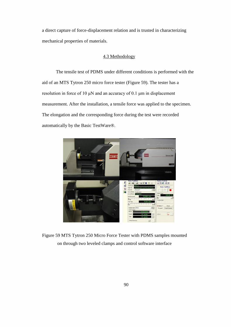
90
a direct capture of force-displacement relation and is trusted in characterizing
mechanical properties of materials.
4.3 Methodology
The tensile test of PDMS under different conditions is performed with the
aid of an MTS Tytron 250 micro force tester (Figure 59). The tester has a
resolution in force of 10 μN and an accuracy of 0.1 μm in displacement
measurement. After the installation, a tensile force was applied to the specimen.
The elongation and the corresponding force during the test were recorded
automatically by the Basic TestWare®.
Figure 59 MTS Tytron 250 Micro Force Tester with PDMS samples mounted
on through two leveled clamps and control software interface
91
The stress and strain are calculated according to the geometric information
of the specimen. The strain-stress curve is drawn and analyzed to extract the
mechanical properties of the tested PDMS.
4.3.1 Experiment Method
Silicone RTV 615 (General Electric) and PDMS Sylgard® 184 (Dow
Corning Corporation) were tested. The manufacturers recommend that the pre-
polymer and cross-linker be mixed at a 10:1 weight ratio, respectively. In this
research, PDMS specimens with various mixing ratios of 2:1, 5:1, 7.5:1 10:1,
12.5:1 20:1 and 50:1 were tensile tested. Bonding strength between different
mixing ratio groups was studied. Different lengths and thicknesses were chosen
for PDMS specimens with 10:1 ratio to characterize the effect of scaling law on
PDMS. Tests of PDMS specimens after chemical immersion were also performed
to quantify the effect of various chemical used in microfabrication and biological
analysis.
All prepared samples are mounted onto the micro force tester and a tensile
force is applied until failure. Experimental data is gathered by the computer
software and processed according to Hook’s Law.
4.3.2 Specimen Design
The tensile test specimens are prepared following the ASTM standard
ASTM D 412 test standard for vulcanized rubber and thermoplastic elastomers -
tension[108]
. The dog-bone shaped test samples are made one-fifth of the standard
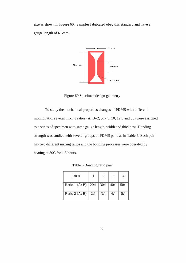
92
size as shown in Figure 60. Samples fabricated obey this standard and have a
gauge length of 6.6mm.
Figure 60 Specimen design geometry
To study the mechanical properties changes of PDMS with different
mixing ratio, several mixing ratios (A: B=2, 5, 7.5, 10, 12.5 and 50) were assigned
to a series of specimen with same gauge length, width and thickness. Bonding
strength was studied with several groups of PDMS pairs as in Table 5. Each pair
has two different mixing ratios and the bonding processes were operated by
heating at 80C for 1.5 hours.
Table 5 Bonding ratio pair
Pair # 1 2 3 4
Ratio 1 (A: B) 20:1 30:1 40:1 50:1
Ratio 2 (A: B) 2:1 3:1 4:1 5:1
93
In order to study the scaling law effect, some samples were categorized
into two groups. One group was for the study of scaling law effect with different
sample lengths. A group of length (2.2mm, 3.3mm, 4.4mm, 5.5mm, 6.6mm
7.7mm and 8.8mm) were chosen. Another group of PDMS samples have
controlled thickness as 50 μm, 100 μm, 150 μm, 200 μm and 300 μm. The widths
and lengths of the samples remain identical.
Samples in the studies for temperature effect and chemical immersion
effect were all based on the design shown in Figure 60. Samples for temperature
effect study were heated on 100°C, 200°C and 300°C hotplates with different time
periods. Samples for chemical immersion effect were processed in different
solutions for different time length (1/2 hour, 1 hour, 2 hour, 10 hours and 24
hours). All of the samples have a same gauge length of 6.6mm, a same thickness
of 50 µm and a same width of 1.1mm.
4.3.3 Specimen Fabrication
PDMS itself is not a photo-curable material and is difficult to form
patterns as photoresists or other photo-sensitive materials doing UV light exposure.
When making testing specimens, researchers always use doctoral scalpels to cut
bulk PDMS into desired shape. When the samples thickness goes up to millimeter
scale, the material can be treated as bulk material. Patterning method using scalpel
will be then appropriate in fabrications. This technique could bring non-ignorable
errors into the test if considered at a microscale level. In this research, other
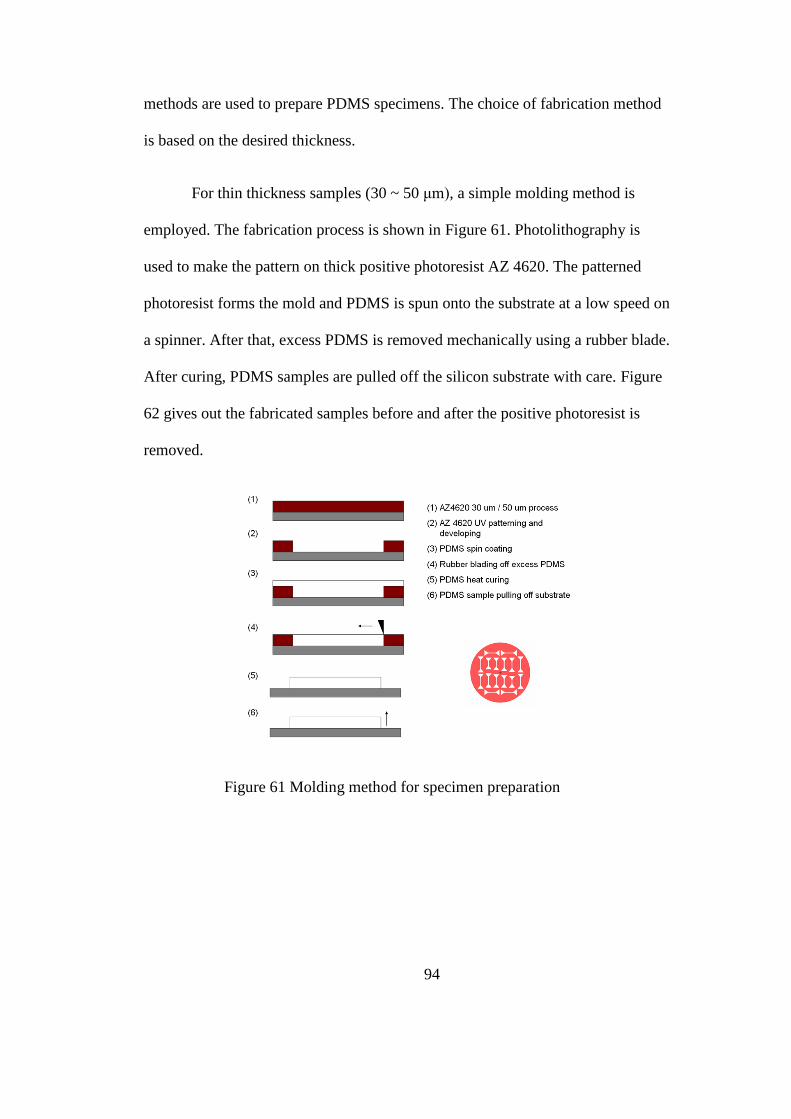
94
methods are used to prepare PDMS specimens. The choice of fabrication method
is based on the desired thickness.
For thin thickness samples (30 ~ 50 μm), a simple molding method is
employed. The fabrication process is shown in Figure 61. Photolithography is
used to make the pattern on thick positive photoresist AZ 4620. The patterned
photoresist forms the mold and PDMS is spun onto the substrate at a low speed on
a spinner. After that, excess PDMS is removed mechanically using a rubber blade.
After curing, PDMS samples are pulled off the silicon substrate with care. Figure
62 gives out the fabricated samples before and after the positive photoresist is
removed.
Figure 61 Molding method for specimen preparation
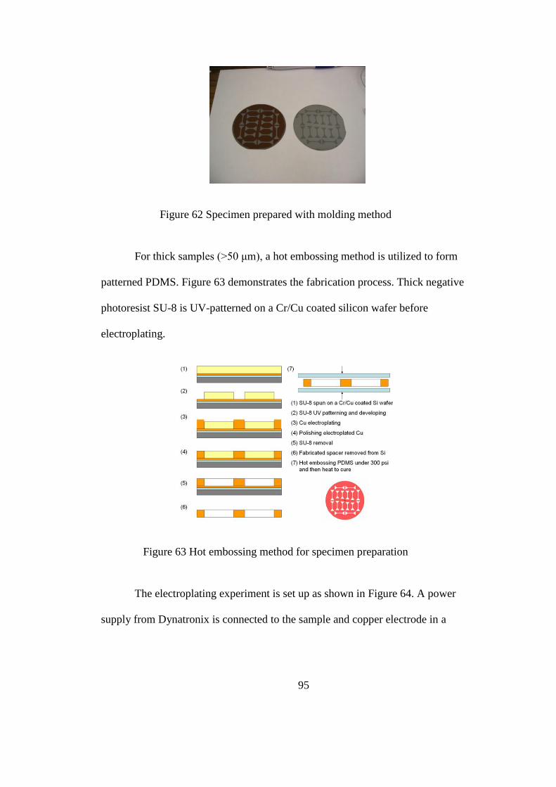
95
Figure 62 Specimen prepared with molding method
For thick samples (>50 μm), a hot embossing method is utilized to form
patterned PDMS. Figure 63 demonstrates the fabrication process. Thick negative
photoresist SU-8 is UV-patterned on a Cr/Cu coated silicon wafer before
electroplating.
Figure 63 Hot embossing method for specimen preparation
The electroplating experiment is set up as shown in Figure 64. A power
supply from Dynatronix is connected to the sample and copper electrode in a
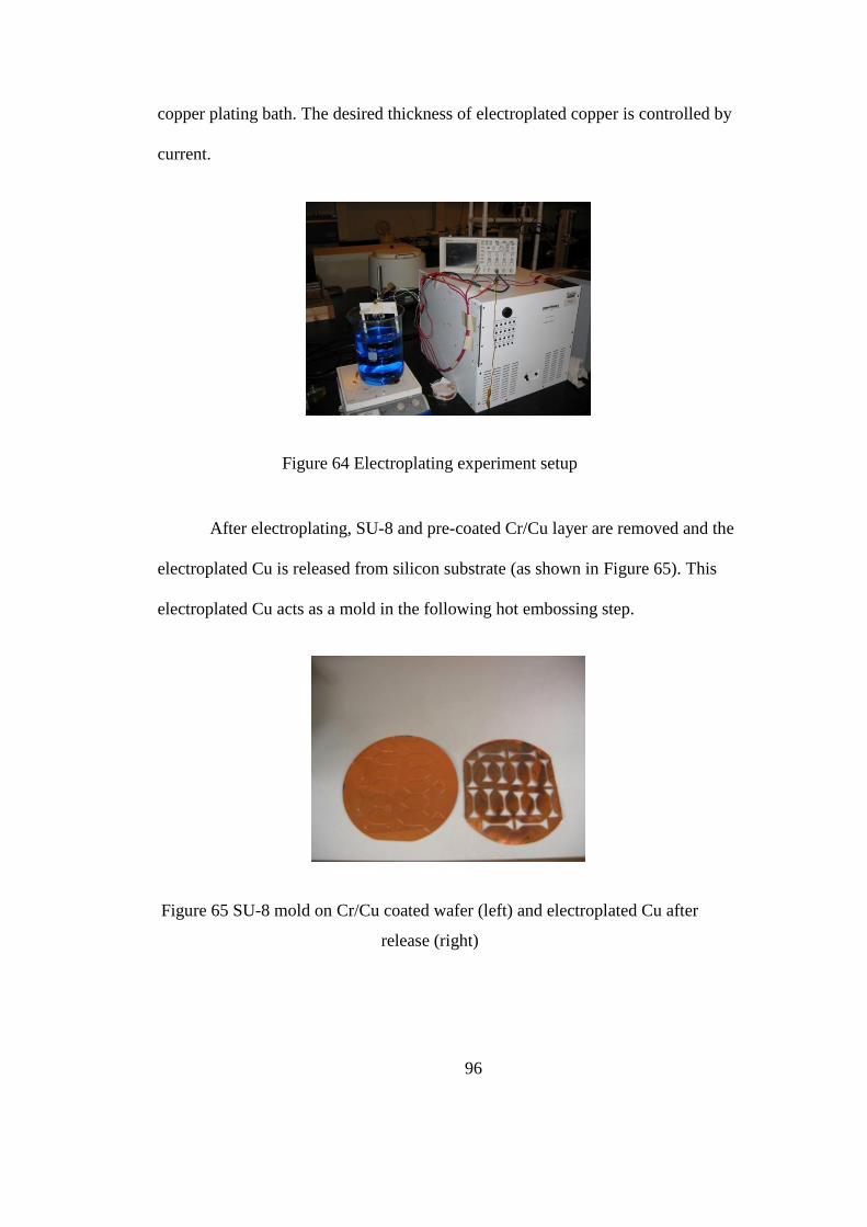
96
copper plating bath. The desired thickness of electroplated copper is controlled by
current.
Figure 64 Electroplating experiment setup
After electroplating, SU-8 and pre-coated Cr/Cu layer are removed and the
electroplated Cu is released from silicon substrate (as shown in Figure 65). This
electroplated Cu acts as a mold in the following hot embossing step.
Figure 65 SU-8 mold on Cr/Cu coated wafer (left) and electroplated Cu after
release (right)
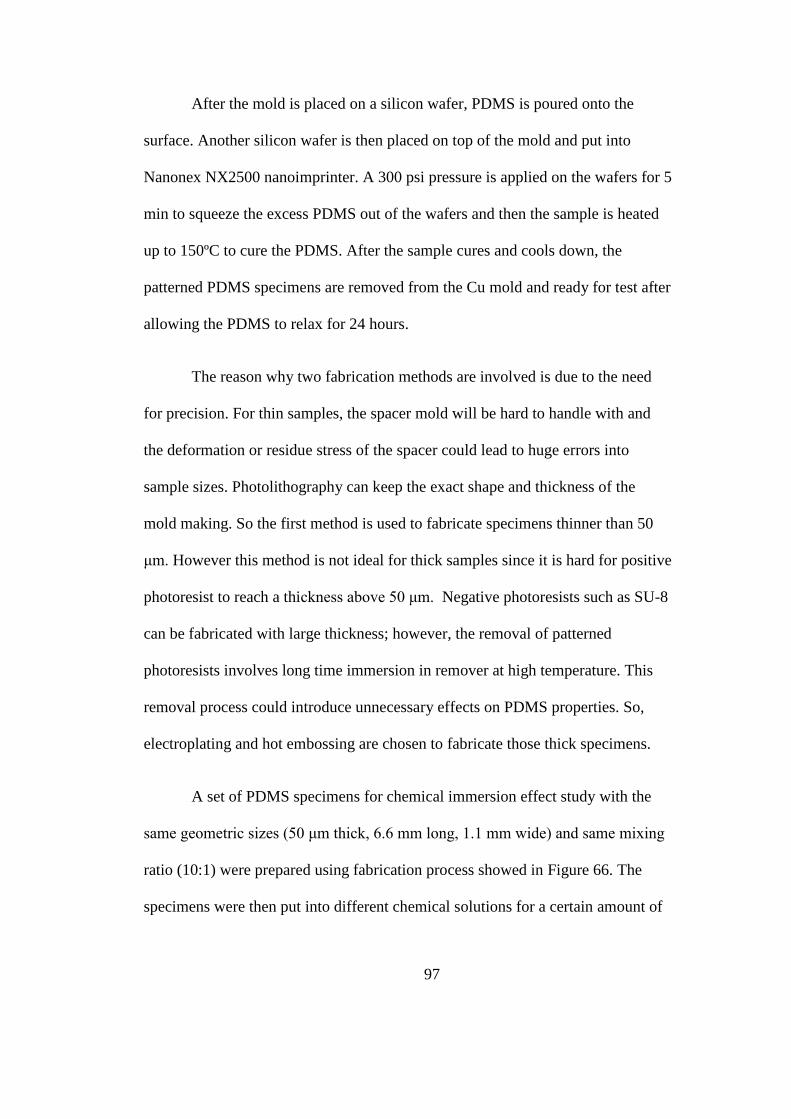
97
After the mold is placed on a silicon wafer, PDMS is poured onto the
surface. Another silicon wafer is then placed on top of the mold and put into
Nanonex NX2500 nanoimprinter. A 300 psi pressure is applied on the wafers for 5
min to squeeze the excess PDMS out of the wafers and then the sample is heated
up to 150ºC to cure the PDMS. After the sample cures and cools down, the
patterned PDMS specimens are removed from the Cu mold and ready for test after
allowing the PDMS to relax for 24 hours.
The reason why two fabrication methods are involved is due to the need
for precision. For thin samples, the spacer mold will be hard to handle with and
the deformation or residue stress of the spacer could lead to huge errors into
sample sizes. Photolithography can keep the exact shape and thickness of the
mold making. So the first method is used to fabricate specimens thinner than 50
μm. However this method is not ideal for thick samples since it is hard for positive
photoresist to reach a thickness above 50 μm. Negative photoresists such as SU-8
can be fabricated with large thickness; however, the removal of patterned
photoresists involves long time immersion in remover at high temperature. This
removal process could introduce unnecessary effects on PDMS properties. So,
electroplating and hot embossing are chosen to fabricate those thick specimens.
A set of PDMS specimens for chemical immersion effect study with the
same geometric sizes (50 μm thick, 6.6 mm long, 1.1 mm wide) and same mixing
ratio (10:1) were prepared using fabrication process showed in Figure 66. The
specimens were then put into different chemical solutions for a certain amount of
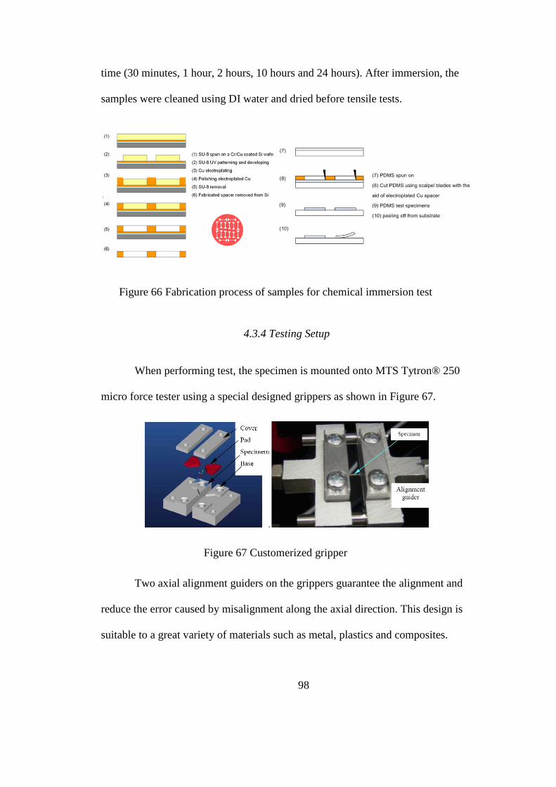
98
time (30 minutes, 1 hour, 2 hours, 10 hours and 24 hours). After immersion, the
samples were cleaned using DI water and dried before tensile tests.
Figure 66 Fabrication process of samples for chemical immersion test
4.3.4 Testing Setup
When performing test, the specimen is mounted onto MTS Tytron® 250
micro force tester using a special designed grippers as shown in Figure 67.
Figure 67 Customerized gripper
Two axial alignment guiders on the grippers guarantee the alignment and
reduce the error caused by misalignment along the axial direction. This design is
suitable to a great variety of materials such as metal, plastics and composites.
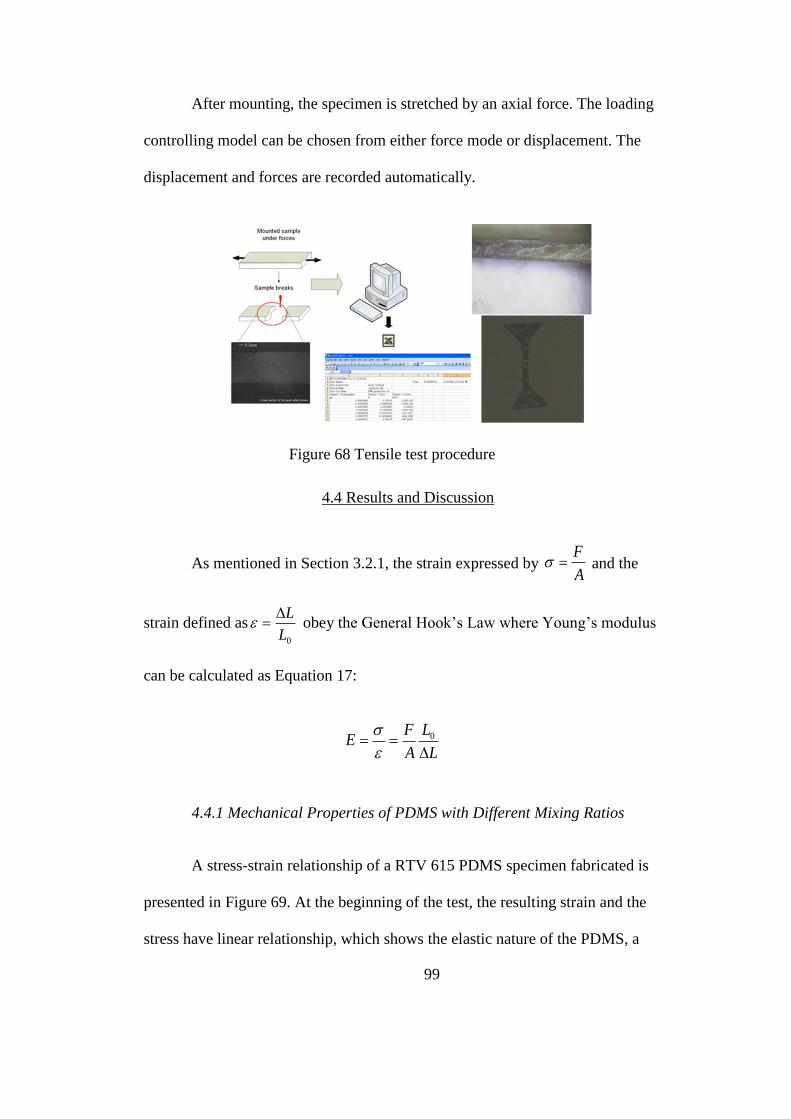
99
After mounting, the specimen is stretched by an axial force. The loading
controlling model can be chosen from either force mode or displacement. The
displacement and forces are recorded automatically.
Figure 68 Tensile test procedure
4.4 Results and Discussion
As mentioned in Section 3.2.1, the strain expressed by A
F and the
strain defined as0L
L obey the General Hook’s Law where Young’s modulus
can be calculated as Equation 17:
L
L
A
FE
0
4.4.1 Mechanical Properties of PDMS with Different Mixing Ratios
A stress-strain relationship of a RTV 615 PDMS specimen fabricated is
presented in Figure 69. At the beginning of the test, the resulting strain and the
stress have linear relationship, which shows the elastic nature of the PDMS, a
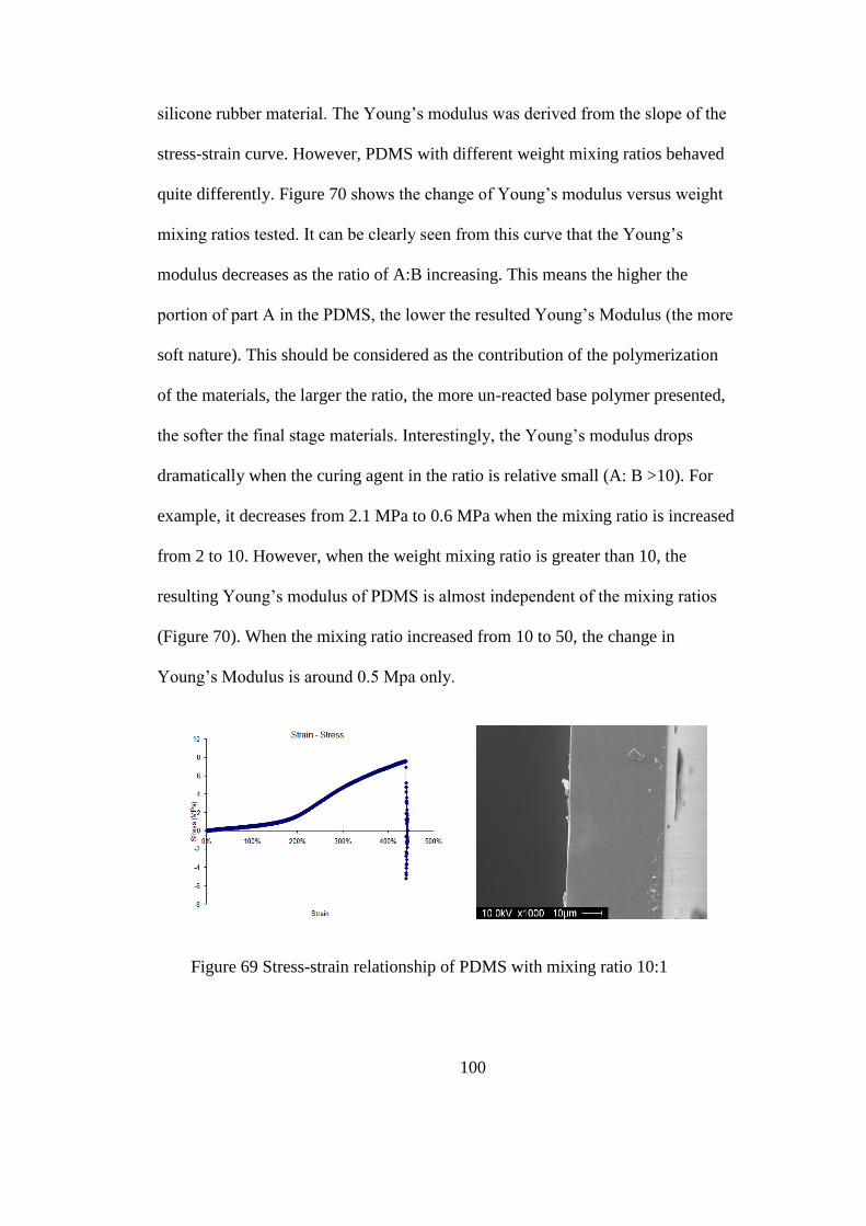
100
silicone rubber material. The Young’s modulus was derived from the slope of the
stress-strain curve. However, PDMS with different weight mixing ratios behaved
quite differently. Figure 70 shows the change of Young’s modulus versus weight
mixing ratios tested. It can be clearly seen from this curve that the Young’s
modulus decreases as the ratio of A:B increasing. This means the higher the
portion of part A in the PDMS, the lower the resulted Young’s Modulus (the more
soft nature). This should be considered as the contribution of the polymerization
of the materials, the larger the ratio, the more un-reacted base polymer presented,
the softer the final stage materials. Interestingly, the Young’s modulus drops
dramatically when the curing agent in the ratio is relative small (A: B >10). For
example, it decreases from 2.1 MPa to 0.6 MPa when the mixing ratio is increased
from 2 to 10. However, when the weight mixing ratio is greater than 10, the
resulting Young’s modulus of PDMS is almost independent of the mixing ratios
(Figure 70). When the mixing ratio increased from 10 to 50, the change in
Young’s Modulus is around 0.5 Mpa only.
Figure 69 Stress-strain relationship of PDMS with mixing ratio 10:1
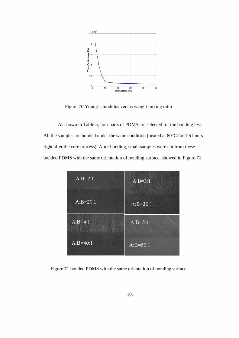
101
Figure 70 Young’s modulus versus weight mixing ratio
As shown in Table 5, four pairs of PDMS are selected for the bonding test.
All the samples are bonded under the same condition (heated at 80°C for 1.5 hours
right after the cure process). After bonding, small samples were cut from these
bonded PDMS with the same orientation of bonding surface, showed in Figure 71.
Figure 71 bonded PDMS with the same orientation of bonding surface
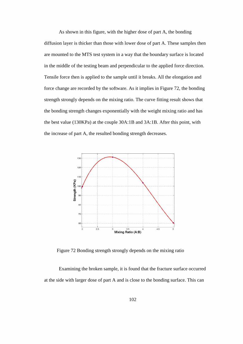
102
As shown in this figure, with the higher dose of part A, the bonding
diffusion layer is thicker than those with lower dose of part A. These samples then
are mounted to the MTS test system in a way that the boundary surface is located
in the middle of the testing beam and perpendicular to the applied force direction.
Tensile force then is applied to the sample until it breaks. All the elongation and
force change are recorded by the software. As it implies in Figure 72, the bonding
strength strongly depends on the mixing ratio. The curve fitting result shows that
the bonding strength changes exponentially with the weight mixing ratio and has
the best value (130KPa) at the couple 30A:1B and 3A:1B. After this point, with
the increase of part A, the resulted bonding strength decreases.
Figure 72 Bonding strength strongly depends on the mixing ratio
Examining the broken sample, it is found that the fracture surface occurred
at the side with larger dose of part A and is close to the bonding surface. This can
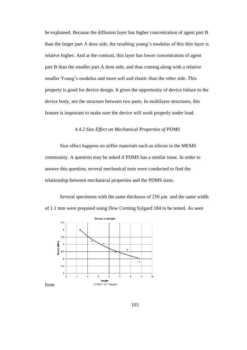
103
be explained. Because the diffusion layer has higher concentration of agent part B
than the larger part A dose side, the resulting young’s modulus of this thin layer is
relative higher. And at the contrast, this layer has lower concentration of agent
part B than the smaller part A dose side, and thus coming along with a relative
smaller Young’s modulus and more soft and elastic than the other side. This
property is good for device design. It gives the opportunity of device failure to the
device body, not the structure between two parts. In multilayer structures, this
feature is important to make sure the device will work properly under load.
4.4.2 Size Effect on Mechanical Properties of PDMS
Size effect happens on stiffer materials such as silicon in the MEMS
community. A question may be asked if PDMS has a similar issue. In order to
answer this question, several mechanical tests were conducted to find the
relationship between mechanical properties and the PDMS sizes.
Several specimens with the same thickness of 250 μm and the same width
of 1.1 mm were prepared using Dow Corning Sylgard 184 to be tested. As seen
from
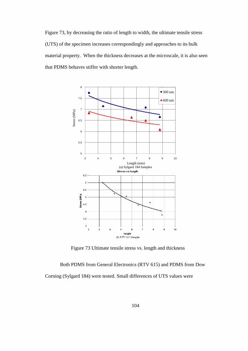
104
Figure 73, by decreasing the ratio of length to width, the ultimate tensile stress
(UTS) of the specimen increases correspondingly and approaches to its bulk
material property. When the thickness decreases at the microscale, it is also seen
that PDMS behaves stiffer with shorter length.
Figure 73 Ultimate tensile stress vs. length and thickness
Both PDMS from General Electronics (RTV 615) and PDMS from Dow
Corning (Sylgard 184) were tested. Small differences of UTS values were
5
5.5
6
6.5
7
7.5
8
3 4 5 6 7 8 9 10
Str
ess
(MP
a)
Length (mm)
(a) Sylgard 184 Samples
300 um
600 um
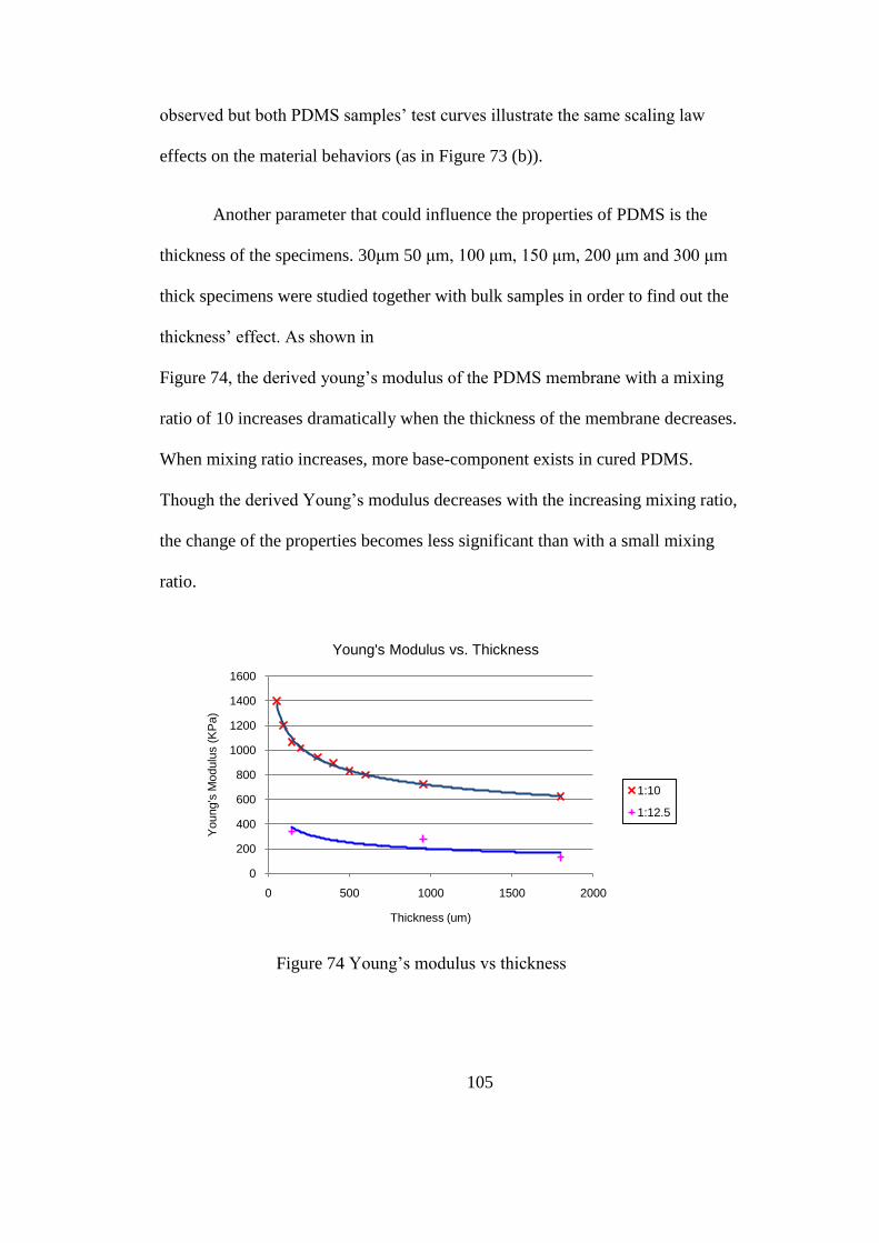
105
observed but both PDMS samples’ test curves illustrate the same scaling law
effects on the material behaviors (as in Figure 73 (b)).
Another parameter that could influence the properties of PDMS is the
thickness of the specimens. 30μm 50 μm, 100 μm, 150 μm, 200 μm and 300 μm
thick specimens were studied together with bulk samples in order to find out the
thickness’ effect. As shown in
Figure 74, the derived young’s modulus of the PDMS membrane with a mixing
ratio of 10 increases dramatically when the thickness of the membrane decreases.
When mixing ratio increases, more base-component exists in cured PDMS.
Though the derived Young’s modulus decreases with the increasing mixing ratio,
the change of the properties becomes less significant than with a small mixing
ratio.
Figure 74 Young’s modulus vs thickness
0
200
400
600
800
1000
1200
1400
1600
0 500 1000 1500 2000
Young's
Modulu
s (
KP
a)
Thickness (um)
Young's Modulus vs. Thickness
1:10
1:12.5
106
Taking all of the parameters of the sizes into effect, it is clear that the
scaling law does apply to PDMS at micro-scale. When the PDMS membrane’s
thickness decreases, the material behaves stiffer than in its bulk material status.
Derived Young’s modulus of PDMS at microscale is approximate twice of the
value for its bulk material. With the geometry sizes down, the Young’s modulus
increases and the material behaves stiffer. At millimeter scale, scaling law effect
trails off and the mechanical properties of PDMS approach to the characteristics
of bulk materials.
4.4.3 Chemical Immersion Effects on Mechanical Properties of PDMS
Most microfluidic devices made of PDMS are used in bio-MEMS. The
devices need to be either contacted or immersed in different solutions used in the
bio-analysis and microfabrication process. Some commonly used solutions in
applications are listed but not limited to Acetone, Methanol, Ethanol, Isopropanol,
PCR buffer, photoresist developers and acids. Even with the natural stability of
polymer, PDMS can still be affected by immersion in these chemicals.
Degradation and properties may change exist during the immersion.
4.4.3.1 Organic Solvents Immersion
Figure 75 presents a stress-strain relationship of PDMS samples after
1hour and 10 hours acetone immersion.
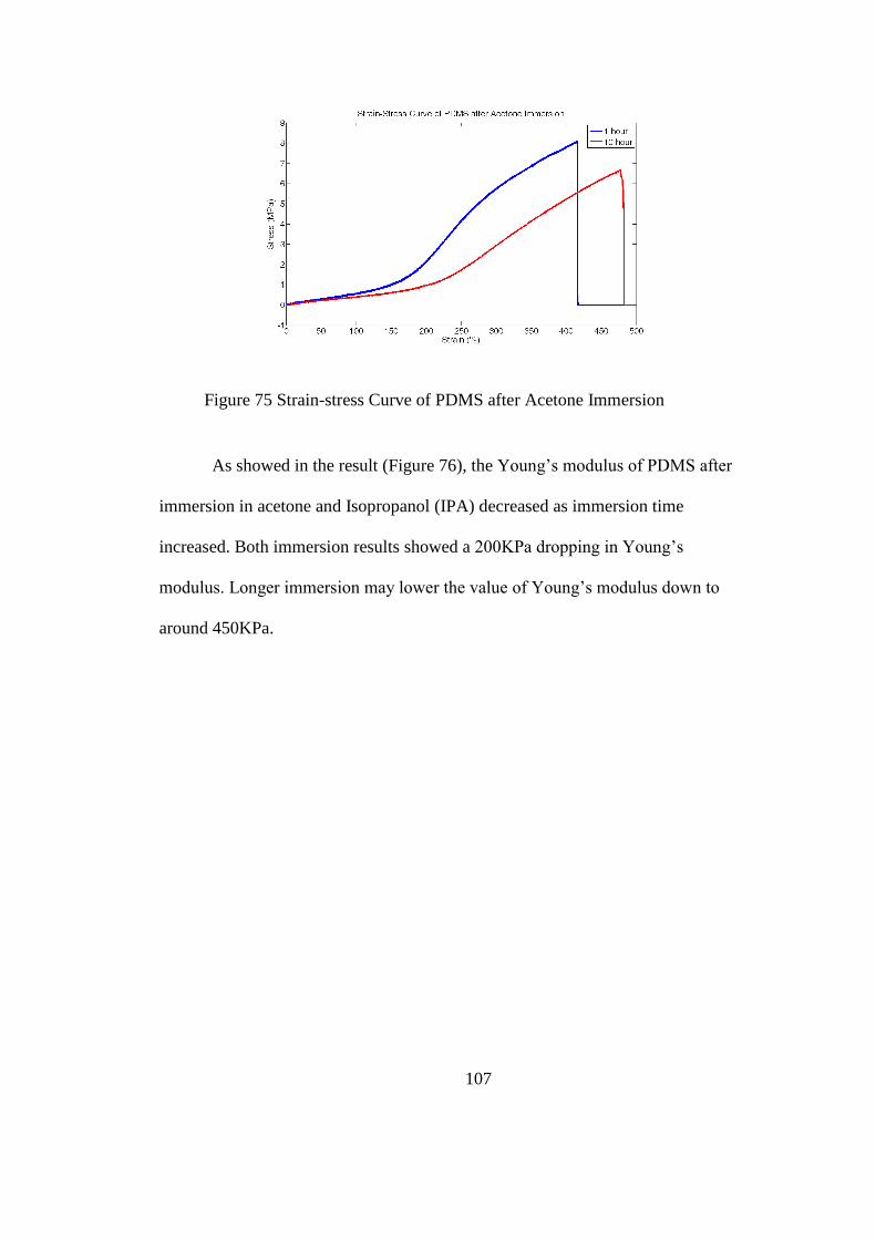
107
Figure 75 Strain-stress Curve of PDMS after Acetone Immersion
As showed in the result (Figure 76), the Young’s modulus of PDMS after
immersion in acetone and Isopropanol (IPA) decreased as immersion time
increased. Both immersion results showed a 200KPa dropping in Young’s
modulus. Longer immersion may lower the value of Young’s modulus down to
around 450KPa.
108
Figure 76 Young’s modulus of PDMS after immersion in Acetone and
Isopropanol
Another two sets of specimens which were immersed in ethanol and
methanol present different tendency (
Figure 77). Higher values of Young’s modulus are noticed with the situation of
longer immersion time. The effects of these two immersions saturated around
750KPa and longer immersion would not result same big influence.
109
Figure 77 Young’s Modulus of PDMS after Immersion in Methanol and Ethanol
The ultimate tensile stress (UTS) is being influenced with chemical
immersions too. Figure 78 shows the change in UTS after different immersion
time in these four organic solvents. For immersion in Acetone and Isopropanol,
results show a decrease in UTS with the time increase. In the same immersion
time series, UTS present an ascending tendency with an increase in immersion
time. Chemical immersions may bring a 2~3MPa change in UTS of PDMS
membrane.
110
Figure 78 Ultimate Tensile Stresses of PDMS after Immersion in Acetone,
Isopropanol, Methanol and Ethanol
Along with the change in UTS after immersion, the elongation of the
PDMS specimens shows a change with immersion (Figure 79). After immersion
in acetone and isopropanol, elongation increases by about 100% with the increase
of immersion time while methanol and ethanol immersion decrease the elongation
by about 100~150%.
111
Figure 79 Elongations of PDMS after Immersion in Acetone, Isopropanol,
Methanol and Ethanol
Chemical reactions on PDMS surfaces may make contributions to these
changes. Organic solvents cause the PDMS specimen to swell or strengthen which
results in a change in mechanical behavior. Swollen PDMS behaves softer than
normal PDMS since the invasive organic solvent weakens its structure. Acetone
and isopropanol are two examples of this mechanism. Another possible reaction
between the organic solvents and PDMS is that the resulted new surface or
structure is more intense which results in a relatively stiffer behavior and higher
UTS with smaller elongation.
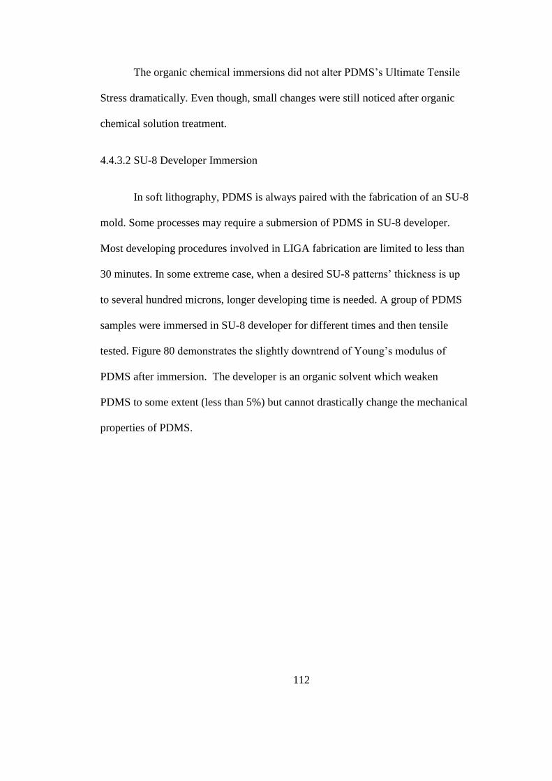
112
The organic chemical immersions did not alter PDMS’s Ultimate Tensile
Stress dramatically. Even though, small changes were still noticed after organic
chemical solution treatment.
4.4.3.2 SU-8 Developer Immersion
In soft lithography, PDMS is always paired with the fabrication of an SU-8
mold. Some processes may require a submersion of PDMS in SU-8 developer.
Most developing procedures involved in LIGA fabrication are limited to less than
30 minutes. In some extreme case, when a desired SU-8 patterns’ thickness is up
to several hundred microns, longer developing time is needed. A group of PDMS
samples were immersed in SU-8 developer for different times and then tensile
tested. Figure 80 demonstrates the slightly downtrend of Young’s modulus of
PDMS after immersion. The developer is an organic solvent which weaken
PDMS to some extent (less than 5%) but cannot drastically change the mechanical
properties of PDMS.
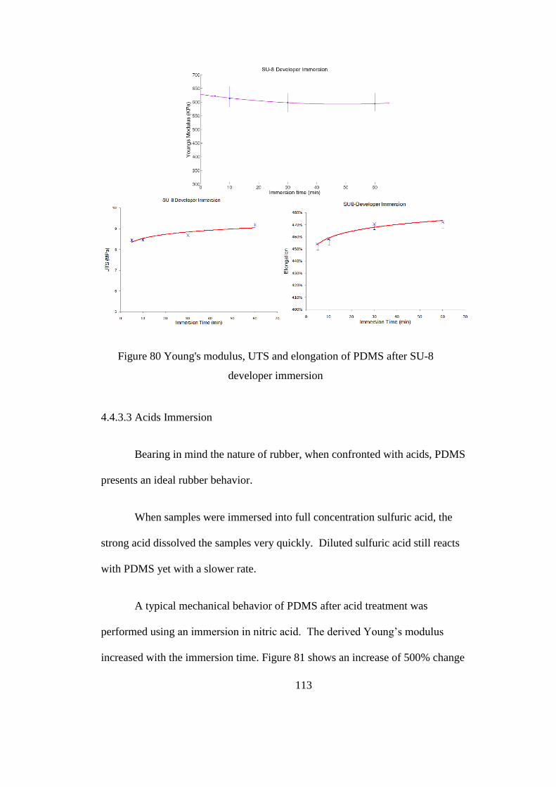
113
Figure 80 Young's modulus, UTS and elongation of PDMS after SU-8
developer immersion
4.4.3.3 Acids Immersion
Bearing in mind the nature of rubber, when confronted with acids, PDMS
presents an ideal rubber behavior.
When samples were immersed into full concentration sulfuric acid, the
strong acid dissolved the samples very quickly. Diluted sulfuric acid still reacts
with PDMS yet with a slower rate.
A typical mechanical behavior of PDMS after acid treatment was
performed using an immersion in nitric acid. The derived Young’s modulus
increased with the immersion time. Figure 81 shows an increase of 500% change
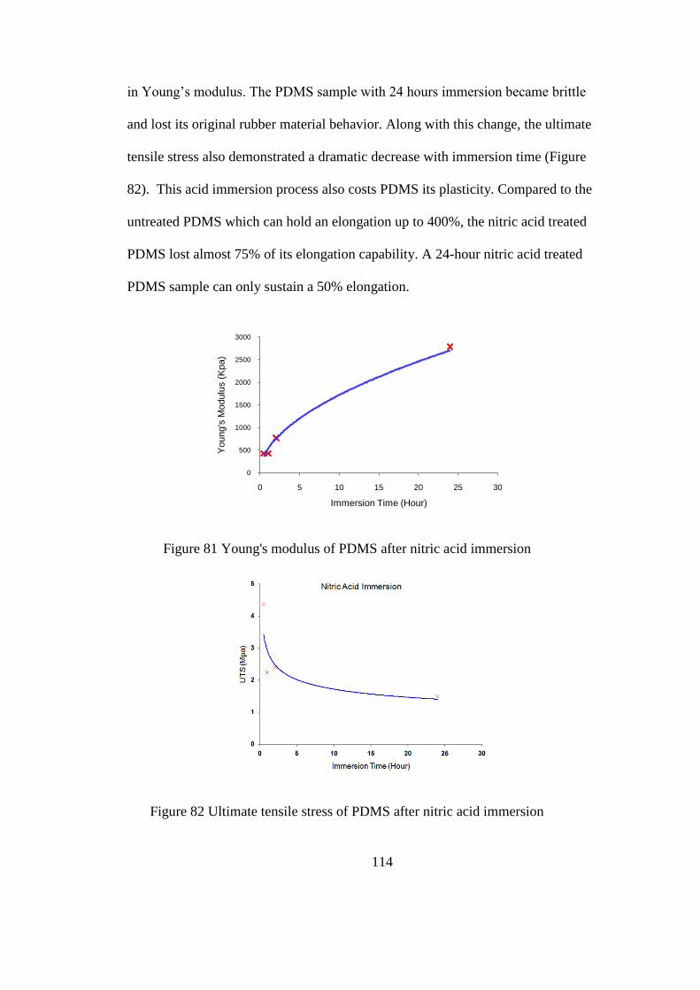
114
in Young’s modulus. The PDMS sample with 24 hours immersion became brittle
and lost its original rubber material behavior. Along with this change, the ultimate
tensile stress also demonstrated a dramatic decrease with immersion time (Figure
82). This acid immersion process also costs PDMS its plasticity. Compared to the
untreated PDMS which can hold an elongation up to 400%, the nitric acid treated
PDMS lost almost 75% of its elongation capability. A 24-hour nitric acid treated
PDMS sample can only sustain a 50% elongation.
Figure 81 Young's modulus of PDMS after nitric acid immersion
Figure 82 Ultimate tensile stress of PDMS after nitric acid immersion
0
500
1000
1500
2000
2500
3000
0 5 10 15 20 25 30
Young's
Modulu
s (
Kpa)
Immersion Time (Hour)
115
Figure 83 Elongation of PDMS after nitric acid immersion
Nitrification may be considered as the major contribution to this property
change of PDMS. The longer the immersion time, the greater the nitrification of
PDMS and the material behaves more brittle and stiff.
4.4.3.4 Electroplating Solutions Immersion
PDMS’s stable chemical characters draw more and more attention from
MEMS researchers. Some of the studies use this rubber material as a mold in
micro-electroplating process to achieve pattern transfer[109]
. This application
requires PDMS mold stay immersed for a relative long time in an electroplating
solution during the experiments. We studied the immersion effects on PDMS with
nickel and copper electroplating solutions.
A typical nickel electroplating solution is prepared following Table 6.
Two temperatures of 45°C and 60°C were used in electroplating and were studied
as different experiment parameters. Each temperature setup occupied one group of
PDMS samples for different immersion time and then tensile tested.
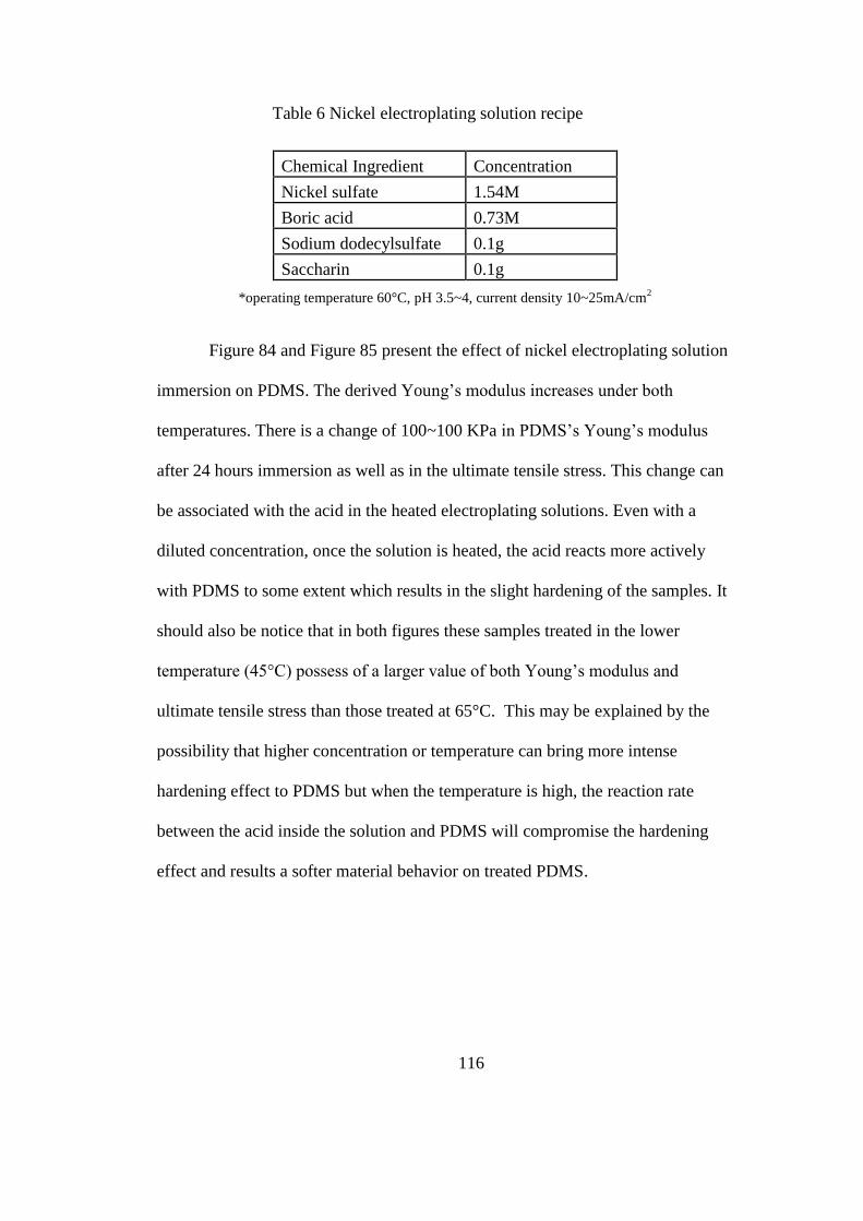
116
Table 6 Nickel electroplating solution recipe
Chemical Ingredient Concentration
Nickel sulfate 1.54M
Boric acid 0.73M
Sodium dodecylsulfate 0.1g
Saccharin 0.1g
*operating temperature 60°C, pH 3.5~4, current density 10~25mA/cm2
Figure 84 and Figure 85 present the effect of nickel electroplating solution
immersion on PDMS. The derived Young’s modulus increases under both
temperatures. There is a change of 100~100 KPa in PDMS’s Young’s modulus
after 24 hours immersion as well as in the ultimate tensile stress. This change can
be associated with the acid in the heated electroplating solutions. Even with a
diluted concentration, once the solution is heated, the acid reacts more actively
with PDMS to some extent which results in the slight hardening of the samples. It
should also be notice that in both figures these samples treated in the lower
temperature (45°C) possess of a larger value of both Young’s modulus and
ultimate tensile stress than those treated at 65°C. This may be explained by the
possibility that higher concentration or temperature can bring more intense
hardening effect to PDMS but when the temperature is high, the reaction rate
between the acid inside the solution and PDMS will compromise the hardening
effect and results a softer material behavior on treated PDMS.
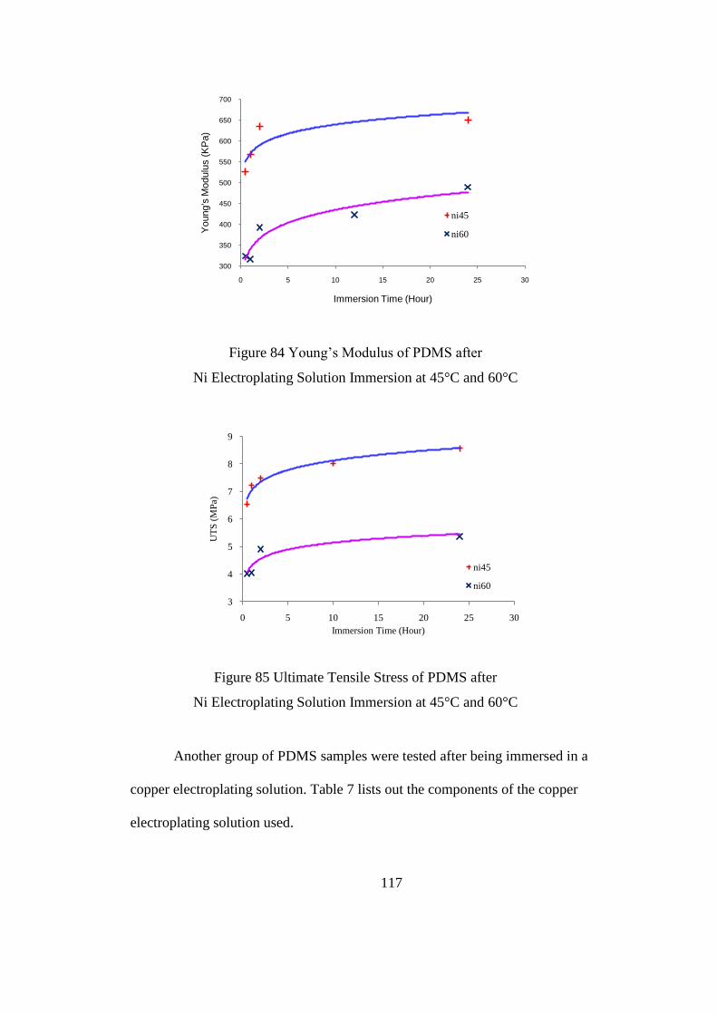
117
Figure 84 Young’s Modulus of PDMS after
Ni Electroplating Solution Immersion at 45°C and 60°C
Figure 85 Ultimate Tensile Stress of PDMS after
Ni Electroplating Solution Immersion at 45°C and 60°C
Another group of PDMS samples were tested after being immersed in a
copper electroplating solution. Table 7 lists out the components of the copper
electroplating solution used.
300
350
400
450
500
550
600
650
700
0 5 10 15 20 25 30
Young's
Modulu
s (
KP
a)
Immersion Time (Hour)
ni45
ni60
3
4
5
6
7
8
9
0 5 10 15 20 25 30
UT
S (
MP
a)
Immersion Time (Hour)
ni45
ni60
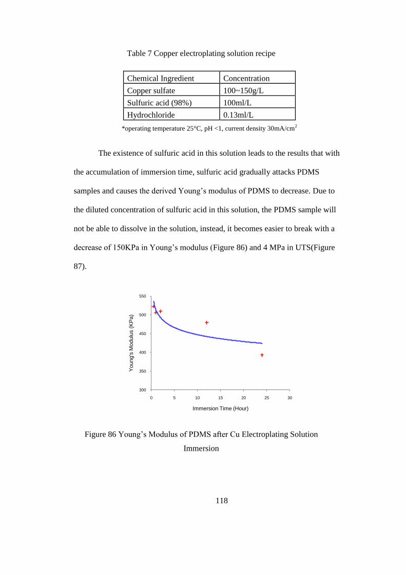
118
Table 7 Copper electroplating solution recipe
Chemical Ingredient Concentration
Copper sulfate 100~150g/L
Sulfuric acid (98%) 100ml/L
Hydrochloride 0.13ml/L
*operating temperature 25°C, pH <1, current density 30mA/cm2
The existence of sulfuric acid in this solution leads to the results that with
the accumulation of immersion time, sulfuric acid gradually attacks PDMS
samples and causes the derived Young’s modulus of PDMS to decrease. Due to
the diluted concentration of sulfuric acid in this solution, the PDMS sample will
not be able to dissolve in the solution, instead, it becomes easier to break with a
decrease of 150KPa in Young’s modulus (Figure 86) and 4 MPa in UTS(Figure
87).
Figure 86 Young’s Modulus of PDMS after Cu Electroplating Solution
Immersion
300
350
400
450
500
550
0 5 10 15 20 25 30
Young's
Modulu
s (
KP
a)
Immersion Time (Hour)
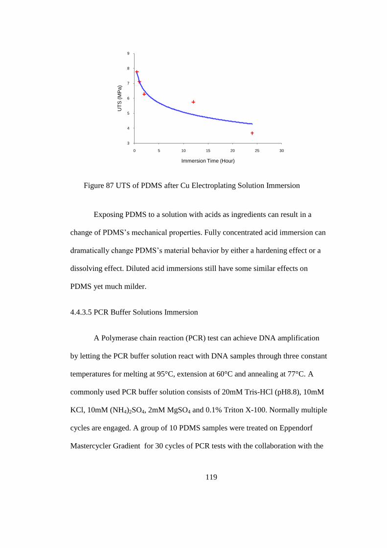
119
Figure 87 UTS of PDMS after Cu Electroplating Solution Immersion
Exposing PDMS to a solution with acids as ingredients can result in a
change of PDMS’s mechanical properties. Fully concentrated acid immersion can
dramatically change PDMS’s material behavior by either a hardening effect or a
dissolving effect. Diluted acid immersions still have some similar effects on
PDMS yet much milder.
4.4.3.5 PCR Buffer Solutions Immersion
A Polymerase chain reaction (PCR) test can achieve DNA amplification
by letting the PCR buffer solution react with DNA samples through three constant
temperatures for melting at 95°C, extension at 60°C and annealing at 77°C. A
commonly used PCR buffer solution consists of 20mM Tris-HCl (pH8.8), 10mM
KCl, 10mM (NH4)2SO4, 2mM MgSO4 and 0.1% Triton X-100. Normally multiple
cycles are engaged. A group of 10 PDMS samples were treated on Eppendorf
Mastercycler Gradient for 30 cycles of PCR tests with the collaboration with the
3
4
5
6
7
8
9
0 5 10 15 20 25 30
UT
S (
MP
a)
Immersion Time (Hour)
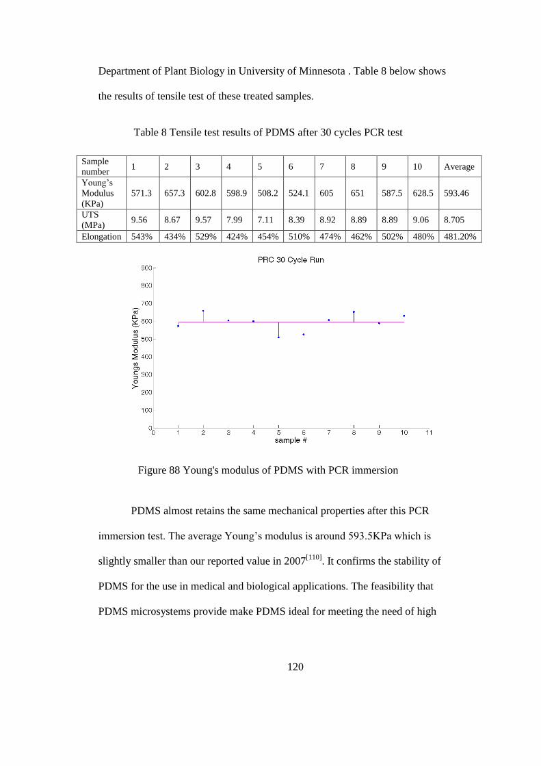
120
Department of Plant Biology in University of Minnesota . Table 8 below shows
the results of tensile test of these treated samples.
Table 8 Tensile test results of PDMS after 30 cycles PCR test
Sample
number 1 2 3 4 5 6 7 8 9 10 Average
Young’s
Modulus
(KPa)
571.3 657.3 602.8 598.9 508.2 524.1 605 651 587.5 628.5 593.46
UTS
(MPa) 9.56 8.67 9.57 7.99 7.11 8.39 8.92 8.89 8.89 9.06 8.705
Elongation 543% 434% 529% 424% 454% 510% 474% 462% 502% 480% 481.20%
Figure 88 Young's modulus of PDMS with PCR immersion
PDMS almost retains the same mechanical properties after this PCR
immersion test. The average Young’s modulus is around 593.5KPa which is
slightly smaller than our reported value in 2007[110]
. It confirms the stability of
PDMS for the use in medical and biological applications. The feasibility that
PDMS microsystems provide make PDMS ideal for meeting the need of high
121
throughput technology in PCR tests and emerge PCR as a powerful tool in not
only genetic analysis, medical diagnostics and also forensic applications.
4.4.4 Temperature Effects on Mechanical Properties of PDMS
In the MEMS applications of PDMS, this soft material is always required
to sustain both a large deformation and a high working temperature, especially
when it is used in a thermal pneumatic driven microsystem. It is necessary to
discover how the material would behave when it is working under a high
temperature for a long time period.
A group of samples were prepared as described in previous section. These
samples were grouped into three sets. Samples were heated on hotplates with
different temperatures of 100°C 200°C and 300°C. Each set correspond to one
temperature. Each set contained 25 samples. Five of them were heated for 30
minutes, five for 1 hour, five for 2 hours and five for 3 hours. Tensile tests of
these samples were presented in Figure 89 and Figure 90.

122
Figure 89 Young’s modulus of PDMS with temperature effect
The values of Young’s modulus for PDMS with temperature effect exhibit
a small decline with the heating time. Higher temperatures result lower Young’s
modulus. The decreases in Young’s modulus at different temperatures were all
smaller than 250K. The ultimate tensile stress also declines with the increase of
heating time as seen in Figure 90. However, this effect became less noticeable
with a high heating temperature.
Figure 90 Ultimate tensile stress of PDMS with temperature effect
123
4.5 Conclusion
The mechanical properties of materials play an important role in the
performance of MEMS devices. However, borrowing the mechanical properties of
materials from macro theories and applying them at micro-scale requires
corrections. When PDMS becomes more and more popular in MEMS applications,
the demand of understanding scaling effects on this material increases.
Direct tensile tests have been conducted to convey the relevant mechanical
properties of PDMS. The results comply with the fact that materials usually
behave differently on the micro-scale. Different parameters that could affect the
resulted PDMS properties have been identified as thickness, length and mixing
ratio. The test results comply with the scaling laws. PDMS with micro-scale size
behaves stiffer with a higher length/width ratio, a thinner thickness or a higher
cross linker mixing ratio.
Material challenges faced by PDMS in MEMS devices often involve not
only structural deformations but also encountering with various chemical
solutions. Micro-scale PDMS samples were treated in commonly used chemical
solutions in microfabrication and direct tensile tests were performed to reveal the
effect. The results comply with the fact that materials could behave differently
after chemical immersions and reveal the influence of chemicals which are
involved in most microfabrication process. As a matter of fact, lots of PDMS-
based micro devices are used for biological analysis, especially PCR. The
performance of PDMS in the presence of PCR buffer solutions is a concern of
124
researchers. The tensile tests were conducted to reveal the effect and affirmed the
good compatibility of PDMS in PCR buffer solution.
Temperature effect on PDMS is also noticed and studied. Long time
operation at high temperature could bring PDMS a decrease in derived Young’s
modulus and an ultimate tensile stress
This detailed tensile test study gives out more accurate mechanical
properties under various operating conditions which can facilitate and accelerate
this material’s various applications in MEMS and bioMEMS devices.
125
CHAPTER 5 CONCLUSION AND OUTLOOK
The work presented in this dissertation was to design a custom
programmable microfluidic system. A systematic study has been conducted on
this system in aspects of design, simulation, fabrication and initial characterization.
An application of this design was adopted into a micromirror array system and
tested as a deformable micromirror. The experimental results have been proven by
finite elements analysis conducted. PDMS is the material of choice for the design
and its properties are important to the success of this study. This research explored
the mechanical properties of PDMS in terms of the effects of scaling law,
chemical immersions and temperatures.
The proposed design has been developed as a PDMS-based programmable
microfluidic system which can provide a universal platform for different
application of microfluidic systems where microflow control is needed regardless
of chemical contact. The developed microfluidic system uses both thermal
pneumatic and electrostatic actuation to realize the action and control of the
microvalve and microflow in the microchannel. A prototype was tested with a 5V
voltage for actuation. Thermal pneumatic simulation optimizes the heat flux at a
value of 5~8×10⁷ W/m
2 to get a better actuation around 1 MHz. A voltage of 50V
is applied to electrostatically drive a 20 µm thick PDMS membrane maintaining a
50µm deflection.
An application of the developed microfluidic system conducted with
specific attention was paid to preliminary results of the system itself and the
126
material properties of PDMS. A sacrificial layer assisted process is presented to
transfer reflective aluminum micromirrors into the PDMS membrane. A
simplified test verified the test result from the finite element analysis. The surface
profile was studied with the help of a Veeco profile system. The deformed
micromirror array maintained good curvature without breaking or peeling off.
PDMS is the major material in the developed devices. Direct tensile tests
were developed to test the mechanical properties of this material both as bulk
material and thin film based MEMS material. PDMS at the manufacturer’s
recommended mixing ratio (10A:1B) has a Young’s modulus of 615KPa as bulk
material. By adjusting the mixing ratio of two PDMS components, different
mechanical properties are gained, which can facilitate researcher by allowing
various desired properties to be considered for their respective designs. As a
MEMS material, the Young’s Modulus and ultimate tensile stress of PDMS vary
in comparison to bulk material properties. Different parameters that could affect
the resulted PDMS properties have been identified as thickness, length to width
ratio and mixing ratio. PDMS at micro-scale size behaves stiffer with a higher
length/width ratio, a thinner thickness or a higher crosslinker mixing ratio. The
use of chemicals and high working temperature during the operation of PDMS-
based microfluidic systems are unavoidable and the chemical immersion effect
and temperature effect on PDMS were characterized.
The results of this study provide fundamentals of developing
programmable microfluidic system by using PDMS. PDMS is biocompatible and
127
cost-efficient solution for many applications including µTAS system, biosensors,
sophisticated optical cross-connects and human retina imagining with its unique
deformability.
Further applications of the custom programmable microfluidic system
would be greatly promoted with expended study of the following suggested
studies:
There are still lots of room to optimize the structure of the microfluidic
system for more efficient and easier fabrication. Integration of control
circuits with the system was not yet been achieved. Characterization of the
microfluidic system is far from enough before using the system in real
µTAS.
PDMS properties changes after chemical immersion still need a more
detailed investigation into the reaction theories of PDMS with chemicals.
This study could be realized with the assistance of Environmental
Scanning Electronic Spectrometer and Fourier Transforms Infrared
Spectroscopy.
As discussed in Chapter 4, the micromirror application encountered
difficulty with holding all the transferred reflective aluminum mirrors due
to the utilization of acetone in removing sacrificial layers. An improved
structure or a primer coating process is needed to improve this adhesion.
Not only would it solve this challenge but also it would further benefit
128
securing the reflective surfaces to PDMS membrane in large deformation
scenario. Further optical characterization of this deformable micromirror
arrays would be able to reveal the detailed relationship between the driven
power and the reflection ability.
In summary, the custom programmable microfluidic system investigated in
this dissertation exhibits tremendous potential in providing a universal platform
for biological and medical analysis application. PDMS’s mechanical properties
make it a novel MEMS material extend the application field even wider into those
fields where large stroke and low power actuation are needed, such as in arrays of
micromirrors. Further research that extends the current work would lead to a
diverse world of new look of microfluidic systems.
129
REFERENCES
1. Terry, S.C., J.H. Jerman, and J.B. Angell, A gas chromatographic air
analyzer fabricated on a silicon wafer. Electron Devices, IEEE
Transactions on, 1979. 26(12): p. 1880-1886.
2. Campbell, L.C., et al., Electrophoretic manipulation of single DNA
molecules in nanofabricated capillaries. Lab on a Chip, 2004. 4(3): p.
225-229.
3. Madou, M.J., et al. A Centrifugal Microfluidic Platform: A Comparison. in
MicroTAS 2000 Symposium. 2000. Enschede, The Netherlands.
4. Johnson, T.J., D. Ross, and L.E. Locascio, Rapid Microfluidic Mixing.
Anal. Chem., 2002. 74(1): p. 45-51.
5. Olsen, K.G., D.J. Ross, and M.J. Tarlov, Immobilization of DNA Hydrogel
Plugs in Microfluidic Channels. Anal. Chem., 2002. 74(6): p. 1436-1441.
6. Joseph Wang, M.P.M.P.C.A.E.R.K.A.G.W.D.H.L., Towards disposable
lab-on-a-chip: Poly(methylmethacrylate) microchip electrophoresis device
with electrochemical detection. ELECTROPHORESIS, 2002. 23(4): p.
596-601.
7. Klank, H., J.P. Kutter, and O. Geschke, CO2-laser micromachining and
back-end processing for rapid production of PMMA-based microfluidic
systems. Lab on a Chip, 2002. 2(4): p. 242-246.
8. Srivastava, Y.N., et al., Polymethylmethacrylate membrane for fluid
encapsulation and release in microfluidic systems. Journal of Vacuum
Science & Technology A: Vacuum, Surfaces, and Films, 2004. 22(3): p.
1067-1072.
9. Locascio, L.E., C.E. Perso, and C.S. Lee, Measurement of electroosmotic
flow in plastic imprinted microfluid devices and the effect of protein
adsorption on flow rate. Journal of Chromatography A, 1999. 857(1-2): p.
275-284.
10. Barker, S.L.R., et al., Plastic Microfluidic Devices Modified with
Polyelectrolyte Multilayers. Anal. Chem., 2000. 72(20): p. 4899-4903.
11. Becker, H. and L.E. Locascio, Polymer microfluidic devices. Talanta, 2002.
56(2): p. 267-287.
12. Chang-Yen, D.A. and B.K. Gale. A PDMS microfluidic spotter for
fabrication of lipid microarrays. in 3rd IEEE/EMBS Special topic
130
conference on microtechnology in medicine and biology. 2005. Kahuku,
HI.
13. Chang-Yen, D.A., D.G. Myszka, and B.K. Gale, A Novel PDMS
Microfluidic Spotter for Fabrication of Protein Chips and Microarrays.
Microelectromechanical Systems, Journal of, 2006. 15(5): p. 1145-1151.
14. Seung-Joon, P., et al. A novel microneedle array integrated with a PDMS
biochip for microfluid systems. in Transducers 03, International
conference on solid-state sensors, actuators and microsystems, Digest of
Techincal Papers, 12th. 2003. Boston, MA.
15. Duffy, D.C., et al., Rapid Prototyping of Microfluidic Systems in
Poly(dimethylsiloxane). Anal. Chem., 1998. 70(23): p. 4974-4984.
16. Unger, M.A., et al., Monolithic Microfabricated Valves and Pumps by
Multilayer Soft Lithography. Science, 2000. 288(5463): p. 113-116.
17. Janasek, D., J. Franzke, and A. Manz, Scaling and the design of
miniaturized chemical-analysis systems. Nature, 2006. 442(7101): p. 374-
380.
18. Jacobson, S.C., et al., Precolumn Reactions with Electrophoretic Analysis
Integrated on a Microchip. Anal. Chem., 1994. 66(23): p. 4127-4132.
19. Burns, M.A., et al., An Integrated Nanoliter DNA Analysis Device. Science,
1998. 282(5388): p. 484-487.
20. Lane, M.E., Microfluidics Technologies, in BCC Research. 2004.
21. Lintel, H.T.G.V., F.C.M.V.D. Pol, and S. Bouwstra, A piezoelectric
micropump based on micro-machinning of silicon. Sensors and Actuators
A, 1989. 15: p. 153.
22. Esashi, M., S. Shoji, and A. Nakano. Normally close microvalve and
micropump fabricated on a silicon wafer. in Micro Electro Mechanical
Systems, 1989, Proceedings, 'An Investigation of Micro Structures,
Sensors, Actuators, Machines and Robots'. IEEE 1989. Salt Lake City,
UT.
23. Zengerle, R., et al., A bidirectional silicon micropump. Sensors and
Actuators A: Physical, 1995. 50(1-2): p. 81-86.
24. Linnemann, R., et al. A self-priming and bubble-tolerant piezoelectric
silicon micropump for liquids and gases. in Micro Electro Mechanical
Systems, 1998. MEMS 98. Proceedings., The Eleventh Annual
International Workshop on 1998. Heidelberg
131
25. Maillefer, D., et al. A high-performance silicon micropump for an
implantable drug delivery system. in Micro Electro Mechanical Systems,
1999. MEMS '99. Twelfth IEEE International Conference on 1999.
Orlando, FL
26. thinXXS, I. XXS2000 Datasheet. ;Available from: www. thinxxxs.com.
27. Kamper, K.P., et al. A self-filling low-cost membrane micropump. in Micro
Electro Mechanical Systems, 1998. MEMS 98. Proceedings., The Eleventh
Annual International Workshop on 1998. Heidelberg.
28. Van de Pol, F.C.M., et al., A thermopneumatic micropump based on
micro-engineering techniques. Sensors and Actuators A: Physical, 1990.
21(1-3): p. 198-202.
29. Zdelblick, M.J. and J.B. Angel. A microminiature electric-to-fluidic valve.
in Transducer '87. 1987. Piscataway, NJ.
30. Zimmermann, S., et al. A planar micropump utilizing thermopneumatic
actuation and in-plane flap valves. in Micro Electro Mechanical Systems,
2004. 17th IEEE International Conference on. (MEMS) 2004.
31. Judy, J.W., T. Tamagawa, and D.L. Polla. Surface-machined
micromechanical membrane pump. in Micro Electro Mechanical Systems,
1991, MEMS '91, Proceedings. 'An Investigation of Micro Structures,
Sensors, Actuators, Machines and Robots'. IEEE 1991. Nara.
32. Rapp, R., et al., LIGA micropump for gases and liquids. Sensors and
Actuators A: Physical, 1994. 40(1): p. 57-61.
33. C, G. and T.Y. C. A thermopneumatic peristaltic micropump. in
Transducer 1999. 1999. Sendai, Japan.
34. Meng, E., et al. A check-valved silicone diaphragm pump. in Micro Electro
Mechanical Systems, 2000. MEMS 2000. The Thirteenth Annual
International Conference on 2000. Miyazaki, Japan.
35. Grover, W.H., et al., Monolithic membrane valves and diaphragm pumps
for practical large-scale integration into glass microfluidic devices.
Sensors and Actuators B: Chemical, 2003. 89(3): p. 315-323.
36. Benard, W.L., et al., Thin-film shape-memory alloy actuated micropumps.
Microelectromechanical Systems, Journal of, 1998. 7(2): p. 245-251.
37. Dario, P., et al., A fluid handling system for a chemical microanalyzer.
Journal of Micromechanics and Microengineering, 1996. 6(1): p. 95.
132
38. Bohm, S., W. Olthuis, and P. Bergveld, A plastic micropump constructed
with conventional techniques and materials. Sensors and Actuators A:
Physical, 1999. 77(3): p. 223-228.
39. R., M.J., Continuum Electromechanics. 1981: Cambridge, Mass. : MIT
Press, c1981.
40. Fuhr, G., T. Schnelle, and B. Wagner, Travelling wave-driven
microfabricated electrohydrodynamic pumps for liquids. Journal of
Micromechanics and Microengineering, 1994. 4(4): p. 217.
41. Richter, A., et al., A micromachined electrohydrodynamic (EHD) pump.
Sensors and Actuators A: Physical, 1991. 29(2): p. 159-168.
42. Liu, S. and P.K. Dasgupta, Flow-injection analysis in the capillary format
using electroosmotic pumping. Analytica Chimica Acta, 1992. 268(1): p.
1-6.
43. Manz, A., et al., Planar chips technology for miniaturization and
integration of separation techniques into monitoring systems : Capillary
electrophoresis on a chip. Journal of Chromatography A, 1992. 593(1-2):
p. 253-258.
44. Manz, A., et al., Electroosmotic pumping and electrophoretic separations
for miniaturized chemical analysis systems. Journal of Micromechanics
and Microengineering, 1994. 4(4): p. 257.
45. R, K.M. Commercialized and emerging lab-on-a-chip applications. in
Micro-total-analysis-system (uTAS) 2001 Symposium. 2001. Monterey,
CA.
46. Jacobson, S.C., et al., Open Channel Electrochromatography on a
Microchip. Anal. Chem., 1994. 66(14): p. 2369-2373.
47. Ramsey, R.S. and J.M. Ramsey, Generating Electrospray from Microchip
Devices Using Electroosmotic Pumping. Anal. Chem., 1997. 69(6): p.
1174-1178.
48. H., P.P. and R.D. J., Electrokinetic high pressure hydraulic system.
49. Yao, S. and J.G. Santiago, Porous glass electroosmotic pumps: theory.
Journal of Colloid and Interface Science, 2003. 268(1): p. 133-142.
50. Jang, J. and S.S. Lee, Theoretical and experimental study of MHD
(magnetohydrodynamic) micropump. Sensors and Actuators A: Physical,
2000. 80(1): p. 84-89.
133
51. Lemoff, A.V. and A.P. Lee, An AC magnetohydrodynamic micropump.
Sensors and Actuators B: Chemical, 2000. 63(3): p. 178-185.
52. Drost, M.K., M.R. Beckette, and R.S. Wegeng, Thermodynamic evaluatin
of a microscale heat pump, in HTD (American Society of Mechanical
Engineerings). 1994. p. 35-43.
53. Vainshtein, P. and C. Gutfinger, On electroviscous effects in
microchannels. Journal of Micromechanics and Microengineering, 2002.
12(3): p. 252.
54. Tretheway, D.C. and C.D. Meinhart. Velocity measurements of flow over
hydrophobic microchannel walls. in Micro-Electro-Mechanical-System
(American Society of Mechanical Engineering). 2001.
55. Tang, Z., et al., Electrokinetic flow control for composition modulation in
a microchannel. Journal of Micromechanics and Microengineering, 2002.
12(6): p. 870.
56. Hidrovo, C.H., et al. Experimental investigation and visualization of two-
phase flow and water transport in microchannels. in Proceedings of the
ASME Fluids Engineering division. 2004.
57. Ross, D., T.J. Johnson, and L.E. Locascio, Imaging of Electroosmotic
Flow in Plastic Microchannels. Anal. Chem., 2001. 73(11): p. 2509-2515.
58. Gian Luca, M., Laminar Liquid Flow Through Silicon Microchannels.
Journal of Fluids Engineering, 2004. 126(3): p. 485-489.
59. Wu, H.Y. and P. Cheng, An experimental study of convective heat transfer
in silicon microchannels with different surface conditions. International
Journal of Heat and Mass Transfer, 2003. 46(14): p. 2547-2556.
60. Morini, G.L., M. Spiga, and P. Tartarini, The rarefaction effect on the
friction factor of gas flow in microchannels. Superlattices and
Microstructures, 2004. 35(3-6): p. 587-599.
61. Hornbeck, L.J., 128 x128 deformable mirror device. Electron Devices,
IEEE Transactions on, 1983. 30(5): p. 539-545.
62. Mansell, J.D., et al. Adaptive Optics for Wavefront Correction of High
Average Power Lasers. in Advanced Solid State Laser Meeting (OSA).
2001.
63. Glenn, W.E., Solid state light modulator structure.
64. Kuck, H., et al. Deformable Micromirror Devices As Phase Modulating
High Resolution Light Valves. in Transducer 95. 1995.
134
65. Perreault, J.A., et al., Adaptive optic correction using
microelectromechanical deformable mirrors. Optical Engineering, 2002.
41(3): p. 561-566.
66. Huang, C., et al. Electroactive Polymer Deformable Micromirrors
(EAPDM) for Biomedical Optics. in Material Research Society Symposium.
2004.
67. Divoux, C., et al., Deformable mirror using magnetic membranes:
application to adaptive optics in astrophysics
Deformable mirror using magnetic membranes: application to adaptive optics in
astrophysics. Magnetics, IEEE Transactions on, 1998. 34(5): p. 3564-3567.
68. Michel, B., et al., Printing meets lithography: Soft approaches to high-
resolution patterning. IBM Journal of Research and Development, 2001.
45(5): p. 697.
69. Maher, J., R.L. Schank, and G. Pfister, Elastomeric optical waveguide
modulators. Applied Physics Letters, 1976. 29(5): p. 293-295.
70. McCreedy, T., Rapid prototyping of glass and PDMS microstructures for
micro total analytical systems and micro chemical reactors by
microfabrication in the general laboratory. Analytica Chimica Acta, 2001.
427(1): p. 39-43.
71. Llobera, A., R. Wilke, and S. Buettgenbach. Two-regime hollow PDMS
Abbe prism for u-TAS applications. in NSTI Nanotech 2004, NSTI
Nanotechnology conference and Trade Show. 2004. Boston, MA.
72. Yasukawa, T., et al., Fabrication of Robust 2-D and 3-D Microfluidic
Networks for Lab-on-a-Chip Bioassays. Microelectromechanical Systems,
Journal of, 2005. 14(4): p. 839-846.
73. Choi, K.M. and J.A. Rogers. A new chemical approach for high fidelity,
nano-scale soft lithography. in 29th ACS National Meeting. 2005. San
Diego, CA.
74. Daniel Sang-Won, P., et al., Polydimethylsiloxane-based pattern transfer
process for the post-IC integration of MEMS onto CMOS chips. Journal of
Micromechanics and Microengineering, 2004. 14(3): p. 335.
75. Kim, J.-H., et al., A disposable thermopneumatic-actuated micropump
stacked with PDMS layers and ITO-coated glass. Sensors and Actuators A:
Physical, 2005. 120(2): p. 365-369.
135
76. Yamaguchi, A., et al., Rapid fabrication of electrochemical enzyme sensor
chip using polydimethylsiloxane microfluidic channel. Analytica Chimica
Acta, 2002. 468(1): p. 143-152.
77. Young Shik, S., et al., PDMS-based micro PCR chip with Parylene
coating. Journal of Micromechanics and Microengineering, 2003. 13(5): p.
768.
78. McDonald, J.C. and G.M. Whitesides, Poly(dimethylsiloxane) as a
Material for Fabricating Microfluidic Devices. Acc. Chem. Res., 2002.
35(7): p. 491-499.
79. Whitesides, G.M., et al., Soft Lithography in biology and biochemistry.
Annual Review of Biomedical Engineering, 2001. 3(1): p. 335-373.
80. GESilicones. ; Available from:
http://www.gesilicones.com/siliconesweb/am1/en/documents/datasheets.
81. Fujii, T., PDMS-based microfluidic devices for biomedical applications.
Microelectronic Engineering, 2002. 61-62: p. 907-914.
82. David, A.P. and G.C. Paul, Monolayer-Mediated Patterning of Integrated
Electroceramics. Journal of Electroceramics, 1999. V3(2): p. 163-172.
83. Zhao, X., Y. Xia, and G.M. Whitesides, Fabrication of three-dimensional
microstructures, microtransfer molding. Advanced Materials, 1996. 8(10):
p. 837-840.
84. Beh, W.S., Y. Xia, and D. Qin, Formation of patterned microstructures of
polycrystalline ceramics from precursor polymers using micromolding in
capillaries. Journal of Materials Research, 1999. 14(10): p. 3995.
85. Xia, Y., Replica molding using polymeric materials: A practival toward
nanomanufacturing. Advanced Materials, 1997. 9: p. 147-149.
86. Luan, S., et al., Solvent-assisted polymer-bonding lithography. Journal of
Vacuum Science & Technology B: Microelectronics and Nanometer
Structures, 2005. 23(1): p. 236-241.
87. Kim, E., et al., Solvent-assisted microcontact molding: A convenient
method for fabricating three-dimensional structures on surfaces of
polymers. Advanced Materials, 1997. 9(8): p. 651-654.
88. Rogers, J.A., et al., Using an elastomeric phase mask for sub-100 nm
photolithography in the optical near field. Applied Physics Letters, 1997.
70(20): p. 2658-2660.
136
89. Hesjedal, T. and W. Seidel, Near-field elastomeric mask photolithography
fabrication of high-frequency surface acoustic wave transducers.
Nanotechnology, 2003. 14(1): p. 91.
90. Bernnen, C.E., Cavitation and bubble dynamics. 1995: New York: Oxford
University Press.
91. Shih, T.-K., et al., Fabrication of PDMS (polydimethylsiloxane) microlens
and diffuser using replica molding. Microelectronic Engineering, 2006.
83(11-12): p. 2499-2503.
92. Park, S., et al., Fabricaton of Poly(dimethylsiloxane) Microlens for Laser-
Induced Fluorescence Detection. Japanese Journal of Applied Physics,
2006. 45(6B): p. 5614-5617.
93. Kim, J., K.-H. Jeong, and L.P. Lee, Artificial ommatidia by self-aligned
microlensesand waveguides. Opt. Lett., 2005. 30(1): p. 5-7.
94. Chang-Yen, D.A., et al., A monolithic PDMS waveguide system fabricated
using soft-lithography techniques. Lightwave Technology, Journal of,
2005. 23(6): p. 2088-2093.
95. Aksyuk, V.A., et al. Lucent Microstar micromirror array technology for
large optical crossconnects. in MOEMS and Miniaturized Systems. 2000.
Santa Clara, CA, USA: SPIE.
96. Stewart, J.B., et al., Design and development of a 331-segment tip-tilt-
piston mirror array for space-based adaptive optics. Sensors and
Actuators A: Physical, 2007. 138(1): p. 230-238.
97. Crunteanu, A., et al. Development of a micro-electro-rnechanical
deformable mirror for fiber laser emission modulation. in Optical MEMS
and Their Applications Conference, 2005. IEEE/LEOS International
Conference on. 2005.
98. Doble, N., et al., Use of a microelectromechanical mirror for adaptive
optics in the human eye. Optics Letters, 2002. 27(17): p. 1537-1539.
99. Dirk-Uwe, B., et al. Retinal imaging with a low-cost micromachined
membrane deformable mirror. 2002: SPIE.
100. Prieto, P., et al., Adaptive optics with a programmable phase modulator:
applications in the human eye. Opt. Express, 2004. 12(17): p. 4059-4071.
101. Lacour, S.P., et al., Stretchable gold conductors on elastomeric substrates.
Applied Physics Letters, 2003. 82(15): p. 2404-2406.
137
102. Xiaoyu, J., et al., Polydimethylsiloxane (PDMS)-based spiral channel PCR
chip. Electronics Letters, 2005. 41(16): p. 890-891.
103. Kim, J.A., et al., Fabrication and characterization of a PDMS-glass
hybrid continuous-flow PCR chip. Biochemical Engineering Journal, 2006.
29(1-2): p. 91-97.
104. Xiang, Q., et al., Real Time PCR on Disposable PDMS Chip with a
Miniaturized Thermal Cycler. Biomedical Microdevices, 2005. 7(4): p.
273-279.
105. Alvaro, M., J.F. Aaron, and R. Shuvo, Characterization of
Polydimethylsiloxane (PDMS) Properties for Biomedical
Micro/Nanosystems. Biomedical Microdevices, 2005. V7(4): p. 281-293.
106. Hwa Seng, K., L. Kuo-Kang, and T. Fan-Gang, Characterization of the
mechanical properties of microscale elastomeric membranes. 2005. p. 653.
107. Chasiotis, I. and W. Knauss, A new microtensile tester for the study of
MEMS materials with the aid of atomic force microscopy. Experimental
Mechanics, 2002. 42(1): p. 51-57.
108. ASTM, A.S.f.T.M. 2008 ; Available from: http://www.astm.org/cgi-
bin/SoftCart.exe/STORE/showcart.html?A+mystore+opcn3581+PDF-
D412+1203970149.
109. Park, D.S.W., et al., Polydimethylsiloxane-based pattern transfer process
for the post-IC integration of MEMS onto CMOS chips. Journal of
Micromechanics and Microengineering, 2004. 14: p. 335-340.
110. Liu, M. and Q. Chen, Characterization study of bonded and unbonded
polydimethylsiloxane aimed for bio-micro-electromechanical systems-
related applications. 2007, SPIE. p. 023008.