8051 notes.doc
12
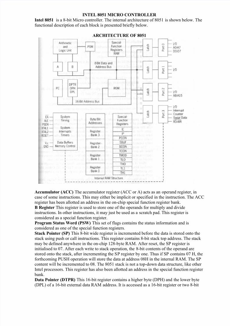
INTEL 8051 MICRO CONTROLLER Intel 8051 is a 8-bit Micro controller. The internal architecture of 8051 is shown below. The functional description of each block is presented briefly below. ARCHITECTURE OF 8051 Accumulator (ACC) The accumulator register (!! or " acts as an operand register# in case of some instructions. This may either be implicit or specified in the instruction. The !! register has been allotted an address in the on-chip special function register bank. B Re!"ter This register is used to store one of the operands for multiply and di$ide instructions. %n other instructions# it may &ust be used as a scratch pad. This register is considered as a special function register. #roram $tatu" %or& (#$%) This set of flags contains the status information and is considered as one of the special function registers. $tac' #o!nter ($#) This 8-bit wide register is incremented before the data is stored onto the stack using push or call instructions. This register contains 8-bit stack top add ress. The stack may be defined anywh ere in the on-chip 1'8-byte M. fter reset# the )* register is initialised to 0+. fter each write to stack operation# the 8-bit contents of the operand are stored onto the stack# after incrementing the )* register by one. Thus if )* contains 0+ ,# the forthcoming *), operation will store the data at address 08, in the internal M. The )* content will be incremented to 08. The 8051 stack is not a top-down data structure# like other %ntel processors. This register has also been allotted an address in the special function register bank. ata #o!nter (T#R) This 1-bit register contains a higher byte (/*," and the lower byte (/*" of a 1-bit eternal data M address. %t is accessed as a 1-bit register or two 8-bit
Transcript of 8051 notes.doc
7/27/2019 8051 notes.doc
http://slidepdf.com/reader/full/8051-notesdoc 1/12
INTEL 8051 MICRO CONTROLLER
Intel 8051 is a 8-bit Micro controller. The internal architecture of 8051 is shown below. The
functional description of each block is presented briefly below.
ARCHITECTURE OF 8051
Accumulator (ACC) The accumulator register (!! or " acts as an operand register# incase of some instructions. This may either be implicit or specified in the instruction. The !!
register has been allotted an address in the on-chip special function register bank.
B Re!"ter This register is used to store one of the operands for multiply and di$ideinstructions. %n other instructions# it may &ust be used as a scratch pad. This register is
considered as a special function register.
#roram $tatu" %or& (#$%) This set of flags contains the status information and is
considered as one of the special function registers.$tac' #o!nter ($#) This 8-bit wide register is incremented before the data is stored onto the
stack using push or call instructions. This register contains 8-bit stack top address. The stack
may be defined anywhere in the on-chip 1'8-byte M. fter reset# the )* register isinitialised to 0+. fter each write to stack operation# the 8-bit contents of the operand are
stored onto the stack# after incrementing the )* register by one. Thus if )* contains 0+ ,# the
forthcoming *), operation will store the data at address 08, in the internal M. The )*content will be incremented to 08. The 8051 stack is not a top-down data structure# like other
%ntel processors. This register has also been allotted an address in the special function register
bank.
ata #o!nter (T#R) This 1-bit register contains a higher byte (/*," and the lower byte
(/*" of a 1-bit eternal data M address. %t is accessed as a 1-bit register or two 8-bit

7/27/2019 8051 notes.doc
http://slidepdf.com/reader/full/8051-notesdoc 2/12
registers as specified abo$e. %t has been allotted two addresses in the special function register bank# for its two bytes /*, and /*.
#ort 0 to Latc*e" an& r!+er" These four latches and dri$er pairs are allotted to each of
the four on-chip %23 ports. These latches ha$e been allotted addresses in the special function
register bank. sing the allotted addresses# the user can communicate with these ports. Theseare identified as *0# *1# *' and *4.
$er!al ata Bu,,er The serial data buffer internally contains two independent registers. 3ne
of them is a transmit buffer which is necessarily a parallel-in serial-out register. The other is
called recei$e buffer which is a serial-in parallel-out register. oading a byte to the transmit buffer initiates serial transmission of that byte. The serial data buffer is identified as )6
and is one of the special function registers. %f a byte is written to )6# it initiates serialtransmission and if the )6 is read# it reads recei$ed serial data.
T!mer Re!"ter" These two 1-bit registers can be accessed as their lower and upper bytes.
7ample# T0 represents the lower byte of the timing register 0# while T,0 represents higher bytes of the timing register 0. )imilarly# T1 and T,1 represent lower and higher bytes of
timing register 1. ll these registers can be accessed using the four addresses allotted to them
which lie in the special function registers )6 address range# i.e.# 80 , to 66.
Control Re!"ter" The special function registers %*# %7# TM3/# T!3# )!3 and *!3contain control and status information for interrupts# timers2counters and serial port. ll of
these registers ha$e been allotted addresses in the special function register bank of 8051.T!m!n an& Control Un!t This unit deri$es all the necessary timing and control signalsre9uired for the internal operation of the circuit. %t also deri$es control signals re9uired for
controlling the eternal system bus.
O"c!llator This circuit generates the basic timing clock signal for the operation of the circuitusing crystal oscillator.
In"truct!on Re!"ter This register decodes the opcode of an instruction to be eecuted and
gi$es information to the timing and control unit to generate necessary signals for the
eecution of the instruction.
#ROM an& #roram A&&re"" Re!"ter These blocks pro$ide an on-chip 7*3M and a
mechanism to internally address it. ote that 7*3M is not a$ailable in all 8051 $ersions.
RAM an& RAM A&&re"" Re!"ter These blocks pro$ide internal 1'8 bytes of M and amechanism to address it internally.
ALU The arithmetic and logic unit performs 8-bit arithmetic and logical operations o$er
operands held by the temporary registers TM*1 and TM*'. sers cannot access thesetemporary registers.
$FR Re!"ter Ban' This is a set of special function registers# which can be addressed usingtheir respecti$e addresses which lie in the range 80, to 66,.
6inally# the interrupt# serial port and timer units control and perform their specific
functions under the control of the timing and control unit.
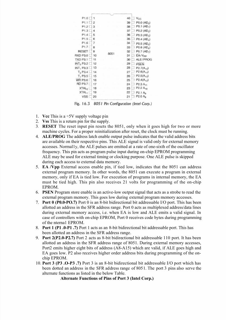
$I-NAL E$CRI#TION$ OF 80518051 is a$ailable in a :0 pin plastic and ceramic /%* packages. The pin diagram of 8051; isshown below followed by description of each pin.
7/27/2019 8051 notes.doc
http://slidepdf.com/reader/full/8051-notesdoc 3/12
1. .cc This is a <5= supply $oltage pin
'. ."" This is a return pin for the supply.4. RE$ET The reset input pin resets the 8051# only when it goes high for two or more
machine cycles. 6or a proper reinitiali>ation after reset# the clock must be running.
:. ALE/#RO- The address latch enable output pulse indicates that the $alid address bitsare a$ailable on their respecti$e pins. This 7 signal is $alid only for eternal memory
accesses. ormal1y# the 7 pulses are emitted at a rate of one-sith of the oscillator
fre9uency. This pin acts as program pulse input during on-chip 7*3M programming7 may be used for eternal timing or clocking purpose. 3ne 7 pulse is skipped
during each access to eternal data memory.
5. EA /. 7ternal access enable pin# if tied low# indicates that the 8051 can addresseternal program memory. %n other words# the 8051 can eecute a program in eternalmemory# only if 7 is tied low. 6or eecution of programs in internal memory# the 7
must be tied high. This pin also recei$es '1 $olts for programming of the on-chip
7*3M.. #$EN *rogram store enable is an acti$e-low output signal that acts as a strobe to read the
eternal program memory. This goes low during eternal program memory accesses.
+. #ort 0 (#002#O3) *ort 0 is an 8-bit bidirectional bit addressable %23 port. This has beenallotted an address in the )6 address range. *ort 0 acts as multipleed address2data lines
during eternal memory access# i.e. when 7 is low and 7 emits a $alid signal. %n
case of controllers with on-chip 7*3M# *ort 0 recei$es code bytes during programming
of the nterna1 7*3M.8. #ort 1 (#1 02#1 3) *ort 1 acts as an 8-bit bidirectional bit addressable port. This has
been allotted an address in the )6 address range.
?. #ort 4(#402#43) *ort ' acts as 8-bit bidirectional bit addressable 110 port. %t has beenallotted an address in the )6 address range of 8051. /uring eternal memory accesses#
*ort' emits higher eight bits of address (8-15" which are $alid# if 7 goes high and
7 goes low. *' also recei$es higher order address bits during programming of the on-chip 7*3M.
10. #ort (# O2# 3) *ort 4 is an 8-bit bidirectional bit addressable %23 port which has
been dotted an address in the )6 address range of 8051. The port 4 pins also ser$e thealternate functions as listed in the below Table.
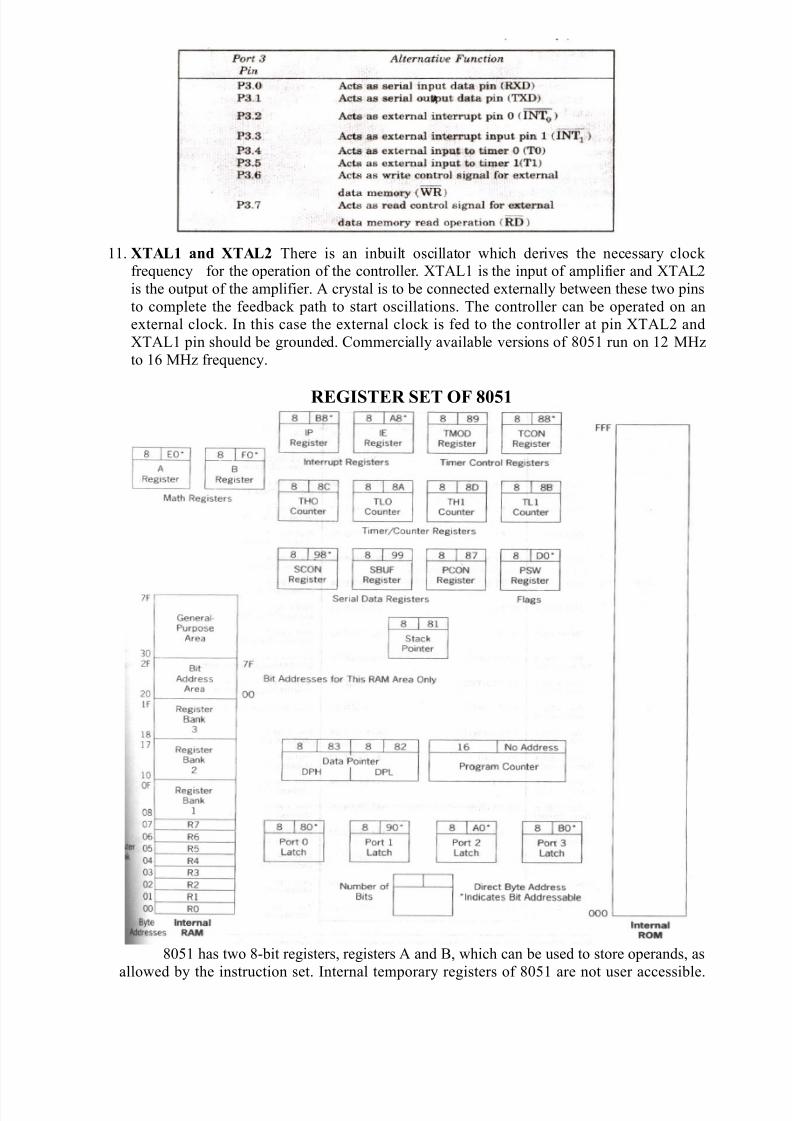
Alternate Funct!on" o, #!n" o, #ort (Intel Cor)
7/27/2019 8051 notes.doc
http://slidepdf.com/reader/full/8051-notesdoc 4/12
11. TAL1 an& TAL4 There is an inbuilt oscillator which deri$es the necessary clockfre9uency for the operation of the controller. @T1 is the input of amplifier and @T'
is the output of the amplifier. crystal is to be connected eternally between these two pins
to complete the feedback path to start oscillations. The controller can be operated on aneternal clock. %n this case the eternal clock is fed to the controller at pin @T' and
@T1 pin should be grounded. !ommercially a$ailable $ersions of 8051 run on 1' M,>
to 1 M,> fre9uency.
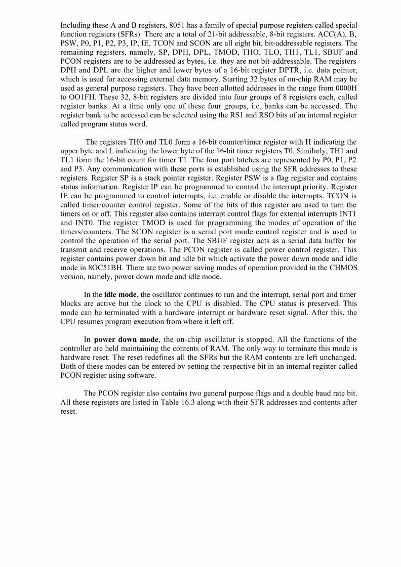
RE-I$TER $ET OF 8051
8051 has two 8-bit registers# registers and # which can be used to store operands# as
allowed by the instruction set. %nternal temporary registers of 8051 are not user accessible.
7/27/2019 8051 notes.doc
http://slidepdf.com/reader/full/8051-notesdoc 5/12
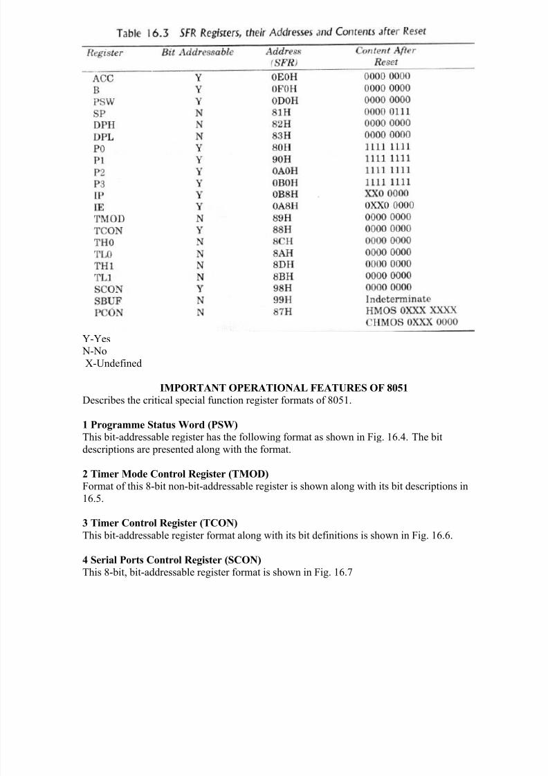
%ncluding these and registers# 8051 has a family of special purpose registers called specialfunction registers ()6s". There are a total of '1-bit addressable# 8-bit registers. !!("# #
*)A# *0# *1# *'# *4# %*# %7# T!3 and )!3 are all eight bit# bit-addressable registers. The
remaining registers# namely# )*# /*,# /*# TM3/# T,3# T3# T,1# T1# )6 and
*!3 registers are to be addressed as bytes# i.e. they are not bit-addressable. The registers/*, and /* are the higher and lower bytes of a 1-bit register /*T# i.e. data pointer#
which is used for accessing eternal data memory. )tarting 4' bytes of on-chip M may be
used as general purpose registers. They ha$e been allotted addresses in the range from 0000,
to 3316,. These 4'# 8-bit registers are di$ided into four groups of 8 registers each# calledregister banks. t a time only one of these four groups# i.e. banks can be accessed. The
register bank to be accessed can be selected using the )1 and )3 bits of an internal registercalled program status word.
The registers T,0 and T0 form a 1-bit counter2timer register with , indicating theupper byte and indicating the lower byte of the 1-bit timer registers T0. )imilarly# T,1 and
T1 form the 1-bit count for timer T1. The four port latches are represented by *0# *1# *'
and *4. ny communication with these ports is established using the )6 addresses to these
registers. egister )* is a stack pointer register. egister *)A is a flag register and containsstatus information. egister %* can be programmed to control the interrupt priority. egister
%7 can be programmed to control interrupts# i.e. enable or disable the interrupts. T!3 iscalled timer2counter control register. )ome of the bits of this register are used to turn thetimers on or off. This register also contains interrupt control flags for eternal interrupts %T1
and %T0. The register TM3/ is used for programming the modes of operation of the
timers2counters. The )!3 register is a serial port mode control register and is used tocontrol the operation of the serial port. The )6 register acts as a serial data buffer for
transmit and recei$e operations. The *!3 register is called power control register. This
register contains power down bit and idle bit which acti$ate the power down mode and idle
mode in 83!51,. There are two power sa$ing modes of operation pro$ided in the !,M3)$ersion# namely# power down mode and idle mode.
%n the !&le mo&e# the oscillator continues to run and the interrupt# serial port and timer blocks are acti$e but the clock to the !* is disabled. The !* status is preser$ed. This
mode can be terminated with a hardware interrupt or hardware reset signal. fter this# the
!* resumes program eecution from where it left off.
%n o6er &o6n mo&e# the on-chip oscillator is stopped. ll the functions of the
controller are held maintaining the contents of M. The only way to terminate this mode ishardware reset. The reset redefines all the )6s but the M contents are left unchanged.
oth of these modes can be entered by setting the respecti$e bit in an internal register called
*!3 register using software.
The *!3 register also contains two general purpose flags and a double baud rate bit.
ll these registers are listed in Table 1.4 along with their )6 addresses and contents after
reset.
7/27/2019 8051 notes.doc
http://slidepdf.com/reader/full/8051-notesdoc 6/12
B-Bes -o
@-ndefined
IM#ORTANT O#ERATIONAL FEATURE$ OF 8051
/escribes the critical special function register formats of 8051.
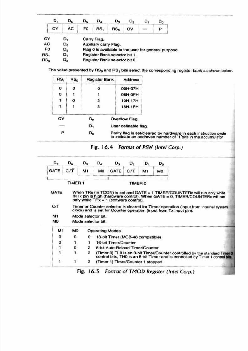
1 #roramme $tatu" %or& (#$%)
This bit-addressable register has the following format as shown in 6ig. 1.:. The bit
descriptions are presented along with the format.
4 T!mer Mo&e Control Re!"ter (TMO)
6ormat of this 8-bit non-bit-addressable register is shown along with its bit descriptions in
1.5.
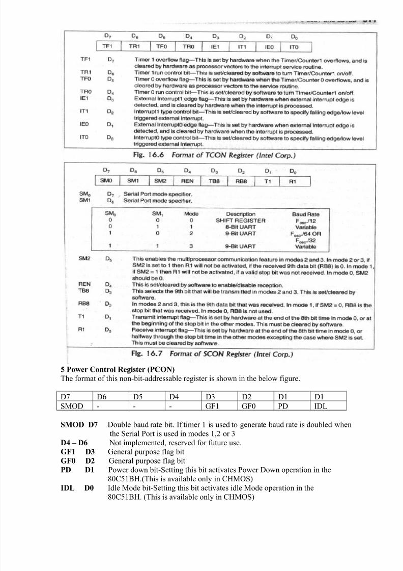
T!mer Control Re!"ter (TCON)
This bit-addressable register format along with its bit definitions is shown in 6ig. 1..
7 $er!al #ort" Control Re!"ter ($CON)
This 8-bit# bit-addressable register format is shown in 6ig. 1.+
7/27/2019 8051 notes.doc
http://slidepdf.com/reader/full/8051-notesdoc 7/12
7/27/2019 8051 notes.doc
http://slidepdf.com/reader/full/8051-notesdoc 8/12
5 #o6er Control Re!"ter (#CON)
The format of this non-bit-addressable register is shown in the below figure.
/+ / /5 /: /4 /' /1 /1)M3/ - - - C61 C60 */ %/
$MO 3 /ouble baud rate bit. %f timer 1 is used to generate baud rate is doubled when
the )erial *ort is used in modes 1#' or 4
7 9 ot implemented# reser$ed for future use.
-F1 Ceneral purpose flag bit
-F0 4 Ceneral purpose flag bit
# 1 *ower down bit-)etting this bit acti$ates *ower /own operation in the 80!51,.(This is a$ailable only in !,M3)"
IL 0 %dle Mode bit-)etting this bit acti$ates idle Mode operation in the
80!51,. (This is a$ailable only in !,M3)"

7/27/2019 8051 notes.doc
http://slidepdf.com/reader/full/8051-notesdoc 9/12
INTERRU#T$ OF 8051
8051 pro$ides fi$e sources of %nterrupts.
INT0 and INT1 are the eternal interrupt inputs. These can be edge sensiti$e or le$elsensiti$e# as programmed with bits IT0 and IT1 in register T!3.These interrupts are
processes internally by the flags %70 and %71.%f the interrupts are programmed edge-sensiti$e#these flags are automatically cleared after the control is transferred to the respecti$e $ector. %f
the interrupt are programmed le$el-sensiti$e# flags are controlled by the eternal interruptssources.
oth timers can be used in timer or counter mode. %n counter mode# it counts the pulses at T0 or T1 pin. %n timer mode# oscillator clock is di$ided by a prescaler (124'" and
then gi$en to the timer. )o clock fre9uency for timer is 124'th of the controller operating
fre9uency. The timer is an up-counter and generates an interrupt when the count has reached
FFFFH. %t can be operated in four different modes that can be set by TMO register.
The timer 0 and timer 1 interrupt sources are generated by TF0 and TF1 bits of theregister T!3# which are set# if a rollo$er takes place in their respecti$e timer registers#
ecept timer 0 in mode 4. Ahen these interrupts are generated# the respecti$e flags are
automatically cleared after the control is transferred to the respecti$e interrupt ser$ice
routines.
The serial port interrupt is generated# if at least one of the two bits 1 and T1 is set.
either of the flags is cleared# after the control is transferred to the interrupt ser$ice routine.The R1 and T1 flags need to be cleared using software# after deciding# which one of these two
caused the interrupt.
%n addition to these fi$e interrupts# 8051 also allows single step interrupts to begenerated with help of software. The eternal interrupts# if programmed le$el-sensiti$e#
should remain high for at least two machine cycles. %f the eternal interrupts are programmed
edge-sensiti$e# they should remain high for at least one machine cycle and low for at least onemachine cycle.
The interrupt structure of 8051 pro$ides two le$els of the interrupt priorities for its sources ofinterrupt. 7ach interrupt source can be programmed to ha$e one of these two le$els using the
interrupt priority register %*. The different sources of interrupts programmed to ha$e the same
le$el of priority# as shown below.
Interrut $ource #r!or!t: 6!t*!n a le+el1. l70 (7ternal %T3" ,ighest
'. T60 (Timer 0"4. %71 (7ternal %T1"
:. T7l (Timer 1"
5. 1 D T1()erial *ort" owest
ll these interrupts are enabled using a special function register called interrupt enable
register (%7" and their priorities are programmed using another special function register calledinterrupt priority register (%*". 6ormats of both of these registers are shown below.

7/27/2019 8051 notes.doc
http://slidepdf.com/reader/full/8051-notesdoc 10/12
ARE$$IN- MOE$ OF 8051
8051 instruction set supports si addressing modes as listed.
1. /irect ddressing'. %ndirect ddressing
4. egister %nstructions
:. egister )pecific (egister %mplicit"5. %mmediate mode
. %ndeed ddressing
The following symbols and their meanings help understanding the addressing modes ofdifferent instructions.
E n E - epresents one of the registers +-0 of the currently selected bank.
E/irect;- epresents 8-bit address of either internal data M or )6 register.EF i; - epresents 8-bit internal data M address addressed indirectly using one of
the registers 0 or 1.
EGdata;- epresents 8-bit immediate data present in an instruction.E G data 1;- epresents 1-bit immediate data present in an instruction.
E addr 1 E -epresents 1-bit destination address which is used by ! or HM*
instruction to specify the call or &ump destination address# within : Ibytes program memory. The label of the &ump address may e$en be directly
specified in the instruction in place of the address.
E addr 11 E -epresents 11-bit destination address# used by ! and HM*
instructions to specify the respecti$e call or &ump addresses within the same ' Ibytes page si>e of the program memory# in which the first byte of the
instruction lies. The label of the &ump address may e$en be directly specified
in the instruction in place of the address.
7/27/2019 8051 notes.doc
http://slidepdf.com/reader/full/8051-notesdoc 11/12
E rel ; - This is a signed 8-bit offset byte in ';s complement form# used by all the!onditional &ump instructions. %t ranges from J1'8 to 1'+ from the first byte
of the instruction. The negati$e offset indicates the backward &ump while the
positi$e offset indicates a forward &ump. The label of the &ump address may
e$en be directly specified in the instruction in place of the address.E bit E - This is a direct accessible bit either in any of the bit addressable special
function registers or the bit addressable area of the internal 1'8 bytes
M# i.e. ('0, to '6,". The bit addressing methods ha$e been discussed in
the pre$ious sections.
1 !rect A&&re""!n %n this mode of addressing# the operands are specified using the 8-bitaddress field# in the instruction format. 3nly internal data M and )6) can be dire
addressed.
7ample K M3= 0# 8?,.,ere 8?, is address of a special function register TM3/.
4 In&!rect A&&re""!n %n this mode of addressing# the 8-bit address of an operand is stored
in a register and the register# instead of the 8-bit address# is specified in the instruction. Theregisters 0 and 1 of the selected bank of registers or stack pointer can be used as address
registers for storing the 8-bit addresses.The address register for 1-bit addresses can only be Edata pointer; (/*T"7ample K // # F 0
Re!"ter In"truct!on" %n this addressing mode# operands are stored in the registers -+ ofthe selected register bank. 3ne of these eight registers (0-+" is specified in the instruction
using the 4-bit register specification field of the opcode format. register bank can be
selected using the two bank select bits of the *)A.
7ample K // # +.
7 Re!"ter $ec!,!c In"truct!on" %n this type of instructions# the operand is implicitly
specified using one of the registers. )ome of the instructions always operate only on a specificregister. These type of instructions fall under this category.
7ampleK L this instruction rotates accumulator left.
5 Imme&!ate Mo&e %n this mode# an immediate data# i.e. a constant is specified in the
instruction# after the opcode byte.
7ample M3= # G133
9 In&e;e& A&&re""!n 3nly program memory can be accessed using this addressing mode.
asically# this mode of addressing is accomplished in 8051 for look-up table manipulations.
*rogram counter or data pointer are allowed 1-bit address storage registers# in this addressingmode.
7ampleK M3= # F /*T
HM* F /*T
7/27/2019 8051 notes.doc
http://slidepdf.com/reader/full/8051-notesdoc 12/12
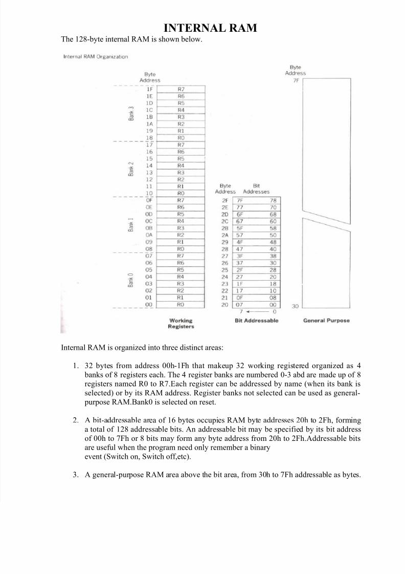
INTERNAL RAMThe 1'8-byte internal M is shown below.
%nternal M is organi>ed into three distinct areasK
1. 4' bytes from address 00h-16h that makeup 4' working registered organi>ed as :
banks of 8 registers each. The : register banks are numbered 0-4 abd are made up of 8registers named 0 to +.7ach register can be addressed by name (when its bank is
selected" or by its M address. egister banks not selected can be used as general-
purpose M.ank0 is selected on reset.
'. bit-addressable area of 1 bytes occupies M byte addresses '0h to '6h# forming
a total of 1'8 addressable bits. n addressable bit may be specified by its bit address
of 00h to +6h or 8 bits may form any byte address from '0h to '6h.ddressable bitsare useful when the program need only remember a binary
e$ent ()witch on# )witch off#etc".
4. general-purpose M area abo$e the bit area# from 40h to +6h addressable as bytes.