
41454C
10
2011 Microchip Technology Inc. Advance Information DS41454C-page 1 PIC12(L)F1501/PIC16(L)F150X High-Performance RISC CPU: • C Compiler Op timiz ed Ar chit ecture • Onl y 49 Instru cti ons • Up to 14 Kb ytes L inear Progra m Memor y Addressing • Up to 5 12 byt es Linear Data Memo ry Addre ssing • Operat ing Speed: - DC – 20 MHz clock input - DC – 125 ns in struct ion c ycl e • Interrupt Capability with Automatic Con text Saving • 16-Le vel Dee p Hardwa re St ack with Option al Overflow/Underflow Reset • Direc t, Ind irect and Relative Addressin g modes: - T wo full 1 6-bit F ile Sel ect Reg isters ( FSRs) - FSRs c an read program and data memory Flexible Oscillator Structure: • 16 MHz Int ernal Oscillator Block: - Fact ory cal ibrat ed to ±1%, typi cal - Soft ware se lect able f requency ran ge from 16 MHz to 31 kHz • 31 kHz Low- Power In ter nal Osci lla tor • Three External Clock modes up to 2 0 MHz Special Microcontroller Features: • Ope rat ing Volt age Ran ge: - 1.8V t o 3.6 V (PIC1 2LF15 01/PI C16LF 150X) - 2.3V to 5 .5V ( PIC12 F1501 /PIC16 F150X) • Self- Progra mmable unde r Soft ware Co ntrol • Power- on Res et (POR) • Power- up Timer (PWRT) • Progra mmable Low-Powe r Brown-Out Reset (LPBOR) • Extended Wat chdog Timer (WDT): - Progra mmabl e peri od from 1 ms to 256s • Pro grammable Code Pro tec tio n • In-Circuit Serial Pro grammi ng™ (ICSP™) via T wo Pins • Enhan ced Low-Vo ltag e Programming (L VP) • Power-Savi ng Sl eep mode: - Low-Power Sle ep mod e - Low-Power BOR (LPBOR) • Inte grate d T empera ture I ndica tor Low-Power Features (PIC12LF1501/PIC16LF150X): • Stan dby Cur ren t: - 20 nA @ 1.8V , typical • Wa tchdog T imer Current: - 300 nA @ 1.8V , t ypic al • Ope rat ing Cur rent: - 30 A/MHz @ 1.8V, typical • Ti mer 1 Osc ill ato r: - 600 n A @ 32 kHz , 1.8 V , typ ical (PIC16LF1508/09 devices only) Peripheral Features: • Analo g-to- Digit al Co nvert er (AD C): - 10-bi t resoluti on - Up t o 12 external cha nnels - 2 i nterna l ch ann els : - Fixed V oltage Ref erence channel - T emperature Indicator channel - Auto acquisition capabilit y - Conve rsion available durin g Sl eep • Up to 2 Compar ators: - Rail-to-rail inputs - Power mode control - Soft ware contro llabl e h ystere sis • Volt age Reference module: - Fixed V olta ge Refere nce (FVR) wi th 1.024 V , 2.048V and 4.096V output levels - Up to 1 r ail-to-rail resis tive 5- bit DAC with positive and negative reference selection • Up to 17 I/O Pins and 1 Input -only Pin: - High current sink/source 2 5 mA/ 25 mA - Indiv idual ly pro grammab le we ak pul l-ups - Individually pro gramma ble interrupt-on- change (IOC) pins • Ti mer0: 8 -Bit T imer/ Count er with 8-Bit Programmable Prescaler • Enhanced Timer1: - 16-bit ti mer/co unter with presca ler - Ext ern al Ga te I nput mode • Ti mer2: 8- Bit Ti mer/Counte r with 8-Bit Pe riod Register, Prescaler and Postscaler • Four 10-bi t PWM module s • Up to 1 Maste r Synchr onous Serial Port (MSSP) with SPI and I 2 C™ with: - 7-bit addres s ma ski ng - SMBus/ PMBus™ compatibility • Up to 1 Enhanced Universal Synchronous Asyn- chronous Receiver Transmitter (EUSART): - RS-232, RS-485 and LIN compa tible 8/14/20-Pin, 8-Bit Flash Microcontrolle rs Product Brief
-
Upload
jorge-garaban -
Category
Documents
-
view
218 -
download
0
Transcript of 41454C

8/3/2019 41454C
http://slidepdf.com/reader/full/41454c 1/10

8/3/2019 41454C
http://slidepdf.com/reader/full/41454c 2/10
PIC12(L)F1501/PIC16(L)F150X
DS41454C-page 2 Advance Information 2011 Microchip Technology Inc.
- Auto-baud detect
- Auto-wake-up on Start
• Up to 4 Configurable Logic Cell (CLC) modules:
- Up to 16 selectable input source signals
- Four inputs per module
- Software control of combinational/sequential
logic/state/clock functions
- AND/OR/XOR/D Flop/D Latch/SR/JK- External or internal inputs/outputs
- Operation while in Sleep
• Numerically Controlled Oscillator (NCO):
- 20-bit accumulator
- 16-bit increment
- True linear frequency control
- High-speed clock input
- Selectable Output modes
- Fixed Duty Cycle (FDC)
- Pulse Frequency Modulation (PFM)
• Complementary Waveform Generator (CWG):
- Up to 8 selectable signal sources
- Selectable falling and rising edge dead-band
control
- Polarity control
- Up to 4 auto-shutdown sources
- Multiple input sources: PWM, CLC, NCO
TABLE 1: PIC12(L)F1501/PIC16(L)F150X FAMILY TYPES
FIGURE 1: 8-PIN PDIP, SOIC, MSOP, DFN DIAGRAM FOR PIC12(L)F1501
DeviceProgram
Memory Flash
(words)
SRAM
(bytes)I/Os
10-bit A/D
(ch)Comparators DAC
Timers
8/16-bitPWM EUSART MSSP CWG CLC NCO ICD XLP
PIC12F1501
PIC12LF15011024 64 6 4 1 1 2/1 4 — — 1 2 1 — —
PIC16F1503
PIC16LF15032048 128 12 8 2 1 2/1 4 — 1 1 2 1 — —
PIC16F1507
PIC16LF15072048 128 18 12 — — 2/1 4 — — 1 2 1 — —
PIC16F1508
PIC16LF15084096 256 18 12 2 1 2/1 4 1 1 1 4 1 V3 X
PIC16F1509
PIC16LF15098192 512 18 12 2 1 2/1 4 1 1 1 4 1 V3 X
Note: Pin details are subject to change.
PDIP, SOIC, MSOP, DFN (2X3)
1
2
3
4
8
7
6
5
VDD
RA5
RA4
MCLR/VPP /RA3
VSS
RA0/ICSPDAT
RA1/ICSPCLK
RA2 P I C 1 2 ( L ) F 1 5 0 1
Note: See Table 2 for location of all peripheral functions.
8/3/2019 41454C
http://slidepdf.com/reader/full/41454c 3/10
2011 Microchip Technology Inc. Advance Information DS41454C-page 3
PIC12(L)F1501/PIC16(L)F150X
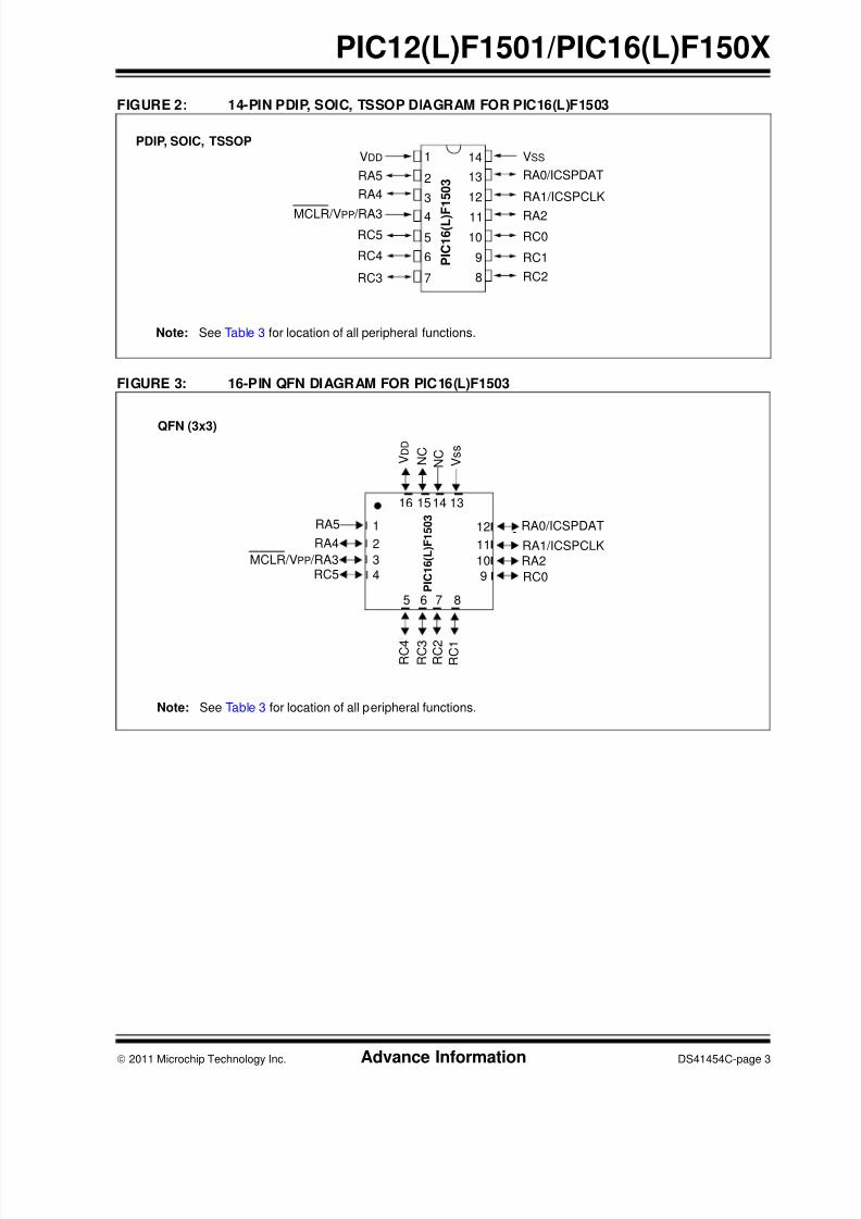
FIGURE 2: 14-PIN PDIP, SOIC, TSSOP DIAGRAM FOR PIC16(L)F1503
FIGURE 3: 16-PIN QFN DIAGRAM FOR PIC16(L)F1503
PDIP, SOIC, TSSOP
P I C 1 6 ( L ) F
1 5 0 3
1
2
3
4
14
13
12
11
5
6
7
10
9
8
VDD
RA5
RA4
MCLR/VPP /RA3
RC5
RC4
RC3
VSS
RA0/ICSPDAT
RA1/ICSPCLK
RA2
RC0
RC1
RC2
Note: See Table 3 for location of all peripheral functions.
Note: See Table 3 for location of all peripheral functions.
-
7 8
2
3
1
11
12
5
9
10
13141516
6
4
RA5
RA4
MCLR/VPP /RA3
R C 4
R C 3
R C 1
R C 2
RC0
RA0/ICSPDAT
RA2
RA1/ICSPCLK
V s s
V D D
N C
RC5
N C
P I C 1 6 ( L ) F 1 5 0 3
QFN (3x3)

8/3/2019 41454C
http://slidepdf.com/reader/full/41454c 4/10
PIC12(L)F1501/PIC16(L)F150X
DS41454C-page 4 Advance Information 2011 Microchip Technology Inc.
FIGURE 4: 20-PIN PDIP, SOIC, SSOP DIAGRAM FOR PIC16(L)F1507/8/9
FIGURE 5: 20-PIN QFN DIAGRAM FOR PIC16(L)F1507/8/9
PDIP, SOIC, SSOP
P I C 1 6 ( L ) F 1 5 0 7 / 8 / 9
1
2
3
4
20
19
18
17
5
6
7
16
15
14
VDD
RA5
RA4
MCLR/VPP /RA3
RC5
RC4
RC3
VSS
RA0/ICSPDAT
RA1/ICSPCLK
RA2
RC0
RC1
RC2
8
9
10
13
12
11
RC6
RC7
RB7
RB4
RB5
RB6
Note 1: See Table 4 for location of all PIC16(L)F1507 peripheral functions.
2: See Table 5 for location of all PIC16(L)F1508/9 peripheral functions
-
8 9
2
3
1
14
15
16
10
11
6
1213
17181920
7
5
4
P I C 1 6 ( L ) F
1 5 0 7 / 8 / 9
MCLR/VPP /RA3RC5
RC4RC3RC6
R C 7
R B 7
R B 4
R B 5
R B 6
RC1RC0
RA2RA1/ICSPCLK
R A 0 / I C S P D A T
V s s
V D D
R A 4
R A 5
RC2
QFN (4x4)
Note 1: See Table 4 for location of all PIC16(L)F1507 peripheral functions.
2: See Table 5 for location of all PIC16(L)F1508/9 peripheral functions
8/3/2019 41454C
http://slidepdf.com/reader/full/41454c 5/10
2011 Microchip Technology Inc. Advance Information DS41454C-page 5
PIC12(L)F1501/PIC16(L)F150X
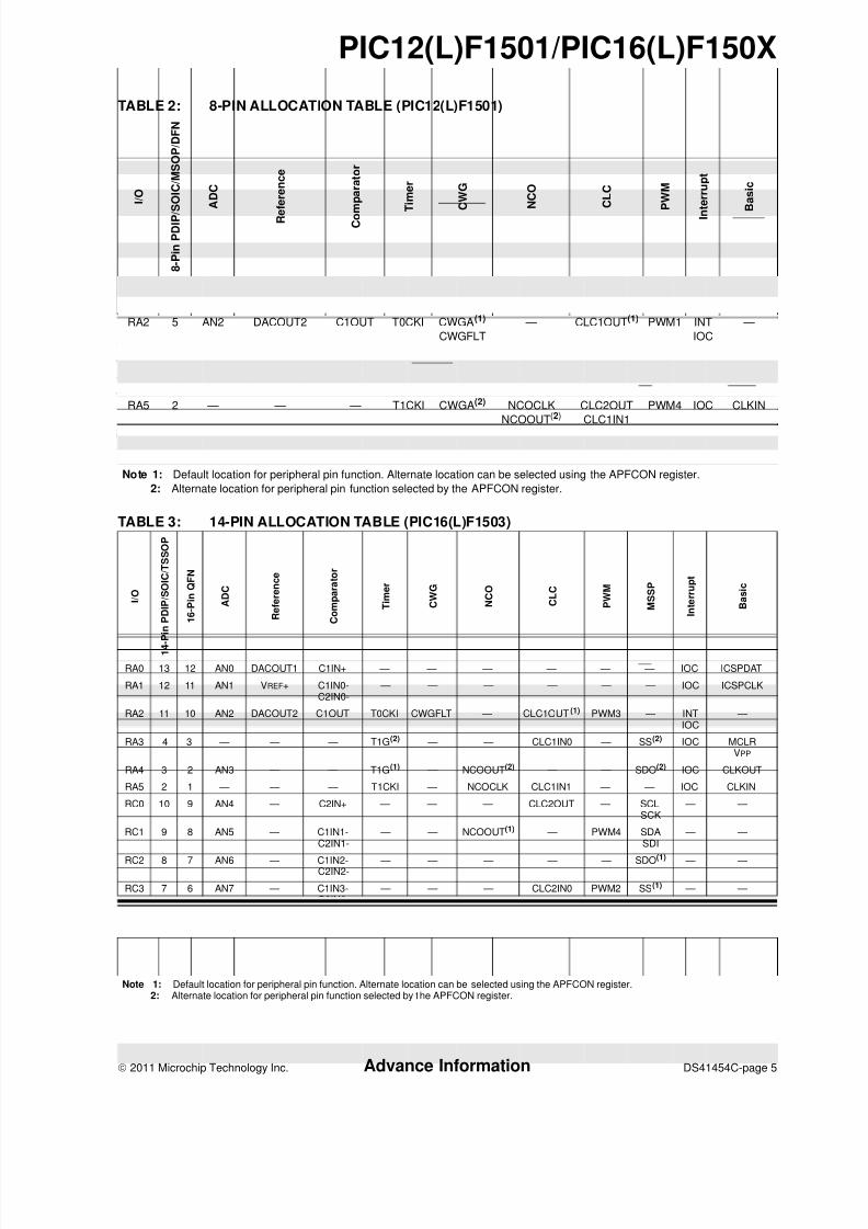
TABLE 2: 8-PIN ALLOCATION TABLE (PIC12(L)F1501)
TABLE 3: 14-PIN ALLOCATION TABLE (PIC16(L)F1503)
I / O
8 - P i n P D I P / S O I C / M S O P / D F N
A D C
R e
f e r e n c e
C o m p a r a t o r
T i m e r
C W G
N C O
C L C
P W M
I n
t e r r u p t
B a s i c
RA0 7 AN0 DACOUT1 C1IN+ — CWGB(1) — CLC2IN1 PWM2 IOC ICSPDAT
RA1 6 AN1 VREF+ C1IN0- — — NCOOUT(1) CLC2IN0 — IOC ICSPCLK
RA2 5 AN2 DACOUT2 C1OUT T0CKI CWGA(1)
CWGFLT
— CLC1OUT(1) PWM1 INT
IOC
—
RA3 4 — — — T1G(2) — — CLC1IN0 — IOC MCLR
VPP
RA4 3 AN3 — C1IN1- T1G(1) CWGB(2) — CLC1OUT(2) PWM3 IOC CLKOUT
RA5 2 — — — T1CKI CWGA(2) NCOCLK
NCOOUT(2)CLC2OUT
CLC1IN1
PWM4 IOC CLKIN
VDD 1 — — — — — — — — — VDD
VSS 8 — — — — — — — — — VSS
Note 1: Default location for peripheral pin function. Alternate location can be selected using the APFCON register.
2: Alternate location for peripheral pin function selected by the APFCON register.
I / O
1 4 - P i n P D I P / S O I C / T S S O P
1 6 - P i n Q F N
A D C
R e f e r e n c e
C o m p a r a t o r
T i m e r
C W G
N C O
C L C
P W M
M S S P
I n t e r r u p t
B a s i c
RA0 13 12 AN0 DACOUT1 C1IN+ — — — — — — IOC ICSPDAT
RA1 12 11 AN1 VREF+ C1IN0-C2IN0-
— — — — — — IOC ICSPCLK
RA2 11 10 AN2 DACOUT2 C1OUT T0CKI CWGFLT — CLC1OUT(1) PWM3 — INTIOC
—
RA3 4 3 — — — T1G(2) — — CLC1IN0 — SS(2) IOC MCLRVPP
RA4 3 2 AN3 — — T1G(1) — NCOOUT(2) — — SDO(2) IOC CLKOUT
RA5 2 1 — — — T1CKI — NCOCLK CLC1IN1 — — IOC CLKIN
RC0 10 9 AN4 — C2IN+ — — — CLC2OUT — SCLSCK
— —
RC1 9 8 AN5 — C1IN1-C2IN1-
— — NCOOUT(1) — PWM4 SDASDI
— —
RC2 8 7 AN6 — C1IN2-C2IN2-
— — — — — SDO(1)
— —
RC3 7 6 AN7 — C1IN3-C2IN3-
— — — CLC2IN0 PWM2 SS(1) — —
RC4 6 5 — — C2OUT — CWGB — CLC2IN1 — — — —
RC5 5 4 — — — — CWGA — CLC1OUT(2) PWM1 — — —
VDD 1 16 — — — — — — — — — — VDD
VSS 14 13 — — — — — — — — — — VSS
Note 1: Default location for peripheral pin function. Alternate location can be selected using the APFCON register.2: Alternate location for peripheral pin function selected by the APFCON register.
8/3/2019 41454C
http://slidepdf.com/reader/full/41454c 6/10
PIC12(L)F1501/PIC16(L)F150X
DS41454C-page 6 Advance Information 2011 Microchip Technology Inc.
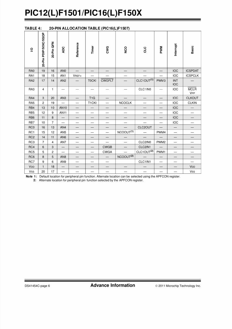
TABLE 4: 20-PIN ALLOCATION TABLE (PIC16(L)F1507)
I / O
2 0 - P i n P D I P / S O I C / S S O P
2
0 - P i n Q F N
A D C
R e f e r e n c e
T i m e r
C W G
N C O
C L C
P W M
I n t e r r u p t
B a s i c
RA0 19 16 AN0 — — — — — — IOC ICSPDAT
RA1 18 15 AN1 VREF+ — — — — — IOC ICSPCLK
RA2 17 14 AN2 — T0CKI CWGFLT — CLC1OUT(1) PWM3 INT
IOC
—
RA3 4 1 — — — — — CLC1IN0 — IOC MCLR
VPP
RA4 3 20 AN3 — T1G — — — — IOC CLKOUT
RA5 2 19 — — T1CKI — NCOCLK — — IOC CLKIN
RB4 13 10 AN10 — — — — — — IOC —
RB5 12 9 AN11 — — — — — — IOC —
RB6 11 8 — — — — — — — IOC —
RB7 10 7 — — — — — — — IOC —
RC0 16 13 AN4 — — — — CLC2OUT — — —
RC1 15 12 AN5 — — — NCOOUT(1) — PWM4 — —
RC2 14 11 AN6 — — — — — — — —
RC3 7 4 AN7 — — — — CLC2IN0 PWM2 — —
RC4 6 3 — — — CWGB — CLC2IN1 — — —
RC5 5 2 — — — CWGA — CLC1OUT(2) PWM1 — —
RC6 8 5 AN8 — — — NCOOUT(2) — — — —
RC7 9 6 AN9 — — — CLC1IN1 — — —
VDD 1 18 — — — — — — — — VDD
VSS 20 17 — — — — — — — — VSSNote 1: Default location for peripheral pin function. Alternate location can be selected using the APFCON register.
2: Alternate location for peripheral pin function selected by the APFCON register.

8/3/2019 41454C
http://slidepdf.com/reader/full/41454c 7/10
2011 Microchip Technology Inc. Advance Information DS41454C-page 7
PIC12(L)F1501/PIC16(L)F150X
TABLE 5: 20-PIN ALLOCATION TABLE (PIC16(L)F1508/9)
I / O
2 0 - P
i n P D I P / S O I C / S S O P
2 0 - P i n Q F N
A D C
R e f e r e n c e
C o m p a r a t o r
T i m e r
C W G
N C O
C L C
P W M
E U S A R T
M S S P
I n t e r r u p t
B a s i c
RA0 19 16 AN0 DACOUT1 C1IN+ — — — — — — — IOC ICSPDATICDDAT
RA1 18 15 AN1 VREF+ C1IN0-C2IN0-
— — — CLC4IN1 — — — IOC ICSPCLKICDCLK
RA2 17 14 AN2 DACOUT2 C1OUT T0CKI CWGFLT — CLC1OUT(1) PWM3 — — INTIOC
—
RA3 4 1 — — — T1G(2) — — CLC1IN0 — — SS(2) IOC MCLRVPP
RA4 3 20 AN3 — — T1OSCOT1G(1)
— — — — — — IOC OSC2CLKOUT
RA5 2 19 — — — T1OSCIT1CKI
— NCOCLK — — — — IOC OSC1CLKIN
RB4 13 10 AN10 — — — — — CLC3IN0 — — SDA
SDI
IOC —
RB5 12 9 AN11 — — — — — CLC4IN0 — RXDX
— IOC —
RB6 11 8 — — — — — — — — — SCLSCK
IOC —
RB7 10 7 — — — — — — CLC3OUT — TXCK
— IOC —
RC0 16 13 AN4 — C2IN+ — — — CLC2OUT — — — — —
RC1 15 12 AN5 — C1IN1-C2IN1-
— — NCOOUT(1) — PWM4 — — — —
RC2 14 11 AN6 — C1IN2-C2IN2-
— — — — — — — — —
RC3 7 4 AN7 — C1IN3-C2IN3-
— — — CLC2IN0 PWM2 — — — —
RC4 6 3 — — C2OUT — CWGB — CLC4OUT
CLC2IN1
— — — — —
RC5 5 2 — — — — CWGA — CLC1OUT(2) PWM1 — — — —
RC6 8 5 AN8 — — — — NCOOUT(2) CLC3IN1 — — SS(1) — —
RC7 9 6 AN9 — — — — — CLC1IN1 — — SDO — —
VDD 1 18 — — — — — — — — — — — VDD
VSS 20 17 — — — — — — — — — — — VSS
Note 1: Default location for peripheral pin function. Alternate location can be selected using the APFCON register.2: Alternate location for peripheral pin function selected by the APFCON register.
8/3/2019 41454C
http://slidepdf.com/reader/full/41454c 8/10
PIC12(L)F1501/PIC16(L)F150X
DS41454C-page 8 Advance Information 2011 Microchip Technology Inc.
NOTES:

8/3/2019 41454C
http://slidepdf.com/reader/full/41454c 9/10
2011 Microchip Technology Inc. Advance Information DS41454C-page 9
Information contained in this publication regarding device
applications and the like is provided only for your convenience
and may be superseded by updates. It is your responsibility to
ensure that your application meets with your specifications.
MICROCHIP MAKES NO REPRESENTATIONS OR
WARRANTIES OF ANY KIND WHETHER EXPRESS OR
IMPLIED, WRITTEN OR ORAL, STATUTORY OR
OTHERWISE, RELATED TO THE INFORMATION,
INCLUDING BUT NOT LIMITED TO ITS CONDITION,
QUALITY, PERFORMANCE, MERCHANTABILITY OR
FITNESS FOR PURPOSE. Microchip disclaims all liability
arising from this information and its use. Use of Microchip
devices in life support and/or safety applications is entirely at
the buyer’s risk, and the buyer agrees to defend, indemnify and
hold harmless Microchip from any and all damages, claims,
suits, or expenses resulting from such use. No licenses are
conveyed, implicitly or otherwise, under any Microchip
intellectual property rights.
Trademarks
The Microchip name and logo, the Microchip logo, dsPIC,
KEELOQ, KEELOQ logo, MPLAB, PIC, PICmicro, PICSTART,
PIC32 logo, rfPIC and UNI/O are registered trademarks of
Microchip Technology Incorporated in the U.S.A. and other
countries.
FilterLab, Hampshire, HI-TECH C, Linear Active Thermistor,
MXDEV, MXLAB, SEEVAL and The Embedded Control
Solutions Company are registered trademarks of Microchip
Technology Incorporated in the U.S.A.
Analog-for-the-Digital Age, Application Maestro, chipKIT,
chipKIT logo, CodeGuard, dsPICDEM, dsPICDEM.net,
dsPICworks, dsSPEAK, ECAN, ECONOMONITOR,FanSense, HI-TIDE, In-Circuit Serial Programming, ICSP,
Mindi, MiWi, MPASM, MPLAB Certified logo, MPLIB,
MPLINK, mTouch, Omniscient Code Generation, PICC,
PICC-18, PICDEM, PICDEM.net, PICkit, PICtail, REAL ICE,
rfLAB, Select Mode, Total Endurance, TSHARC,
UniWinDriver, WiperLock and ZENA are trademarks of
Microchip Technology Incorporated in the U.S.A. and other
countries.
SQTP is a service mark of Microchip Technology Incorporated
in the U.S.A.
All other trademarks mentioned herein are property of their
respective companies.
© 2011, Microchip Technology Incorporated, Printed in the
U.S.A., All Rights Reserved.
Printed on recycled paper.
ISBN: 978-1-61341-392-0
Note the following details of the code protection feature on Microchip devices:
• Microchip products meet the specification contained in their particular Microchip Data Sheet.
• Microchip believes that its family of products is one of the most secure families of its kind on the market today, when used in the
intended manner and under normal conditions.
• There are dishonest and possibly illegal methods used to breach the code protection feature. All of these methods, to our
knowledge, require using the Microchip products in a manner outside the operating specifications contained in Microchip’s DataSheets. Most likely, the person doing so is engaged in theft of intellectual property.
• Microchip is willing to work with the customer who is concerned about the integrity of their code.
• Neither Microchip nor any other semiconductor manufacturer can guarantee the security of their code. Code protection does not
mean that we are guaranteeing the product as “unbreakable.”
Code protection is constantly evolving. We at Microchip are committed to continuously improving the code protection features of our
products. Attempts to break Microchip’s code protection feature may be a violation of the Digital Millennium Copyright Act. If such acts
allow unauthorized access to your software or other copyrighted work, you may have a right to sue for relief under that Act.
Microchip received ISO/TS-16949:2009 certification for its worldwide headquarters, design and wafer fabrication facilities in Chandler and Tempe, Arizona; Gresham, Oregon and design centers in California and India. The Company’s quality system processes and procedures are for its PIC ® MCUs and dsPIC ® DSCs, K EE LOQ ® code hopping devices, Serial EEPROMs, microperipherals, nonvolatile memory and analog products. In addition, Microchip’s quality system for the design and manufacture of development systems is ISO 9001:2000 certified.

8/3/2019 41454C
http://slidepdf.com/reader/full/41454c 10/10
DS41454C-page 10 Advance Information 2011 Microchip Technology Inc.
AMERICASCorporate Office2355 West Chandler Blvd.
Chandler, AZ 85224-6199
Tel: 480-792-7200
Fax: 480-792-7277
Technical Support:
http://www.microchip.com/
support
Web Address:
www.microchip.com
AtlantaDuluth, GA
Tel: 678-957-9614
Fax: 678-957-1455BostonWestborough, MA
Tel: 774-760-0087
Fax: 774-760-0088
ChicagoItasca, IL
Tel: 630-285-0071
Fax: 630-285-0075
ClevelandIndependence, OH
Tel: 216-447-0464
Fax: 216-447-0643
DallasAddison, TX
Tel: 972-818-7423
Fax: 972-818-2924
DetroitFarmington Hills, MI
Tel: 248-538-2250
Fax: 248-538-2260
IndianapolisNoblesville, IN
Tel: 317-773-8323
Fax: 317-773-5453
Los Angeles
Mission Viejo, CA
Tel: 949-462-9523
Fax: 949-462-9608
Santa ClaraSanta Clara, CA
Tel: 408-961-6444
Fax: 408-961-6445
TorontoMississauga, Ontario,
Canada
Tel: 905-673-0699
Fax: 905-673-6509
ASIA/PACIFIC
Asia Pacific Office
Suites 3707-14, 37th Floor
Tower 6, The Gateway
Harbour City, Kowloon
Hong Kong
Tel: 852-2401-1200
Fax: 852-2401-3431
Australia - SydneyTel: 61-2-9868-6733
Fax: 61-2-9868-6755
China - BeijingTel: 86-10-8569-7000
Fax: 86-10-8528-2104
China - Chengdu
Tel: 86-28-8665-5511
Fax: 86-28-8665-7889
China - Chongqing
Tel: 86-23-8980-9588
Fax: 86-23-8980-9500
China - Hangzhou
Tel: 86-571-2819-3180
Fax: 86-571-2819-3189
China - Hong Kong SAR
Tel: 852-2401-1200
Fax: 852-2401-3431
China - Nanjing
Tel: 86-25-8473-2460Fax: 86-25-8473-2470
China - Qingdao
Tel: 86-532-8502-7355
Fax: 86-532-8502-7205
China - ShanghaiTel: 86-21-5407-5533
Fax: 86-21-5407-5066
China - Shenyang
Tel: 86-24-2334-2829
Fax: 86-24-2334-2393
China - Shenzhen
Tel: 86-755-8203-2660
Fax: 86-755-8203-1760
China - WuhanTel: 86-27-5980-5300
Fax: 86-27-5980-5118
China - Xian
Tel: 86-29-8833-7252
Fax: 86-29-8833-7256
China - Xiamen
Tel: 86-592-2388138
Fax: 86-592-2388130
China - Zhuhai
Tel: 86-756-3210040
Fax: 86-756-3210049
ASIA/PACIFIC
India - BangaloreTel: 91-80-3090-4444
Fax: 91-80-3090-4123
India - New Delhi
Tel: 91-11-4160-8631
Fax: 91-11-4160-8632
India - Pune
Tel: 91-20-2566-1512
Fax: 91-20-2566-1513
Japan - Yokohama
Tel: 81-45-471- 6166
Fax: 81-45-471-6122
Korea - DaeguTel: 82-53-744-4301
Fax: 82-53-744-4302
Korea - SeoulTel: 82-2-554-7200
Fax: 82-2-558-5932 or
82-2-558-5934
Malaysia - Kuala Lumpur
Tel: 60-3-6201-9857
Fax: 60-3-6201-9859
Malaysia - Penang
Tel: 60-4-227-8870
Fax: 60-4-227-4068
Philippines - Manila
Tel: 63-2-634-9065Fax: 63-2-634-9069
SingaporeTel: 65-6334-8870
Fax: 65-6334-8850
Taiwan - Hsin Chu
Tel: 886-3-6578-300
Fax: 886-3-6578-370
Taiwan - KaohsiungTel: 886-7-213-7830
Fax: 886-7-330-9305
Taiwan - TaipeiTel: 886-2-2500-6610
Fax: 886-2-2508-0102
Thailand - BangkokTel: 66-2-694-1351
Fax: 66-2-694-1350
EUROPE
Austria - Wels
Tel: 43-7242-2244-39
Fax: 43-7242-2244-393
Denmark - CopenhagenTel: 45-4450-2828
Fax: 45-4485-2829
France - ParisTel: 33-1-69-53-63-20
Fax: 33-1-69-30-90-79
Germany - MunichTel: 49-89-627-144-0
Fax: 49-89-627-144-44
Italy - MilanTel: 39-0331-742611
Fax: 39-0331-466781
Netherlands - Drunen
Tel: 31-416-690399
Fax: 31-416-690340
Spain - MadridTel: 34-91-708-08-90
Fax: 34-91-708-08-91
UK - WokinghamTel: 44-118-921-5869
Fax: 44-118-921-5820
Worldwide Sales and Service
05/02/11


