4 Linear Power Amplifier Integrated Circuits - Educypedia
54
159 4 Linear Power Amplifier Integrated Circuits Introduction The most convenient way to control power to a load is with a power op amp. These op amps have characteristics that are very similar to the low power ICs. However, they may be powered by over 50 V at 5 A. Working with this much voltage and current requires that you accu- rately anticipate the power delivered to the load, the power provided by the dc supplies and the power that the op amp itself must dissipate. The power that the op amp dissipates is converted to heat. To move that heat from the silicon wafer requires effective heat sinking. Should a failure occur (by breakdown of a component, or because you botched the heat sink design), thermal shutdown allows the op amp to turn itself off. On- chip current limiting also allows you to set the maximum current the IC delivers to the load. This protects the load during a failure. Audio power ICs have several special problems. Often you must run them from a single battery. Noise and total harmonic distortion are criti- cal issues, as are circuit features such as bass or treble boost. You will see a low power tabletop amplifier IC and a 56 W boomer IC. Objectives By the end of this chapter, you will be able to: • Determine the gain setting resistors and decoupling capacitors needed by a high voltage, high current, op amp based amplifier. • Calculate the power delivered to the load, provided by the supply and dissipated by the IC. • Calculate the IC and the case temperature and select the heat sink. • Set the short circuit current limiting. • Define special audio amplifier concerns and parameters. • Properly apply a desktop amp, and a high power audio amplifier IC.
Transcript of 4 Linear Power Amplifier Integrated Circuits - Educypedia
159
4 Linear Power Amplifier Integrated Circuits
Introduction The most convenient way to control power to a load is with a power op amp. These op amps have characteristics that are very similar to the low power ICs. However, they may be powered by over 50 V at 5 A.
Working with this much voltage and current requires that you accu-rately anticipate the power delivered to the load, the power provided by the dc supplies and the power that the op amp itself must dissipate. The power that the op amp dissipates is converted to heat. To move that heat from the silicon wafer requires effective heat sinking. Should a failure occur (by breakdown of a component, or because you botched the heat sink design), thermal shutdown allows the op amp to turn itself off. On-chip current limiting also allows you to set the maximum current the IC delivers to the load. This protects the load during a failure.
Audio power ICs have several special problems. Often you must run them from a single battery. Noise and total harmonic distortion are criti-cal issues, as are circuit features such as bass or treble boost. You will see a low power tabletop amplifier IC and a 56 W boomer IC.
Objectives By the end of this chapter, you will be able to:
• Determine the gain setting resistors and decoupling capacitors needed by a high voltage, high current, op amp based amplifier.
• Calculate the power delivered to the load, provided by the supply and dissipated by the IC.
• Calculate the IC and the case temperature and select the heat sink.
• Set the short circuit current limiting.
• Define special audio amplifier concerns and parameters.
• Properly apply a desktop amp, and a high power audio amplifier IC.
Chapter 4 n Linear Power Amplifier Integrated Circuits 160
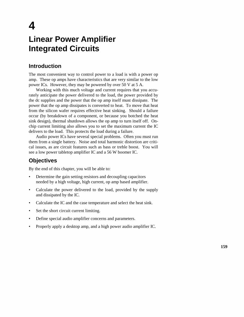
4.1 OPA548 Operational Amplifier IC The OPA548 is a high voltage/high current operational amplifier made by Burr-Brown. Its schematic symbol is shown in Figure 4-1. It is available in two packages, a staggered lead, 7 pin TO-220 package, and a surface mount DDPAK. These are given in Figure 4-2. The circuit board footprints are shown in Figure 4-3. If you want only to output positive voltage to the load, this op amp may be powered from a single supply, as high as +60 V. Connect V− to the circuit common. Unlike older designs, when powered from a single supply the OPA548 operates correctly with the input signal as much as a half of a volt below ground. The minimum single supply voltage is 8 V. So you will have to provide a separate, higher, more powerful supply if the rest of your system is running from +5 V. To drive the load either positive or negative, reversing the direction of a motor, or to send audio to a loudspeaker, you can run the OPA548 from split supplies. Typically this means the dual supplies may range from ±4 V to ±30 V. But as long as the total difference between the power pins is 60 V or less, any combination of supply voltages is ac-ceptable. Just remember to assure that the voltage on each input also always lies between V+ and V− . Only CMOS implemented op amps are able to drive their output voltage all the way to the supplies. Typically the maximum output is several volts smaller than the supplies. This difference between supply voltage and maximum output voltage is called the saturation voltage. For the OPA548, the saturation voltage may be as large as 4 V. With supplies of ±28 V, the output voltage may be no more than 24 Vp. The OPA548 can source or sink up to 5 A to the load. This is an instantaneous (peak) value. So, be sure to use the correct peak to root-mean-squared relationship and peak to average equations. These are summarized in Table 3-1. There are two other factors that limit the in-stantaneous current. You can connect a resistor between the Ilim pin (pin 3) and V− (pin 4). This resistor limits the maximum current to a value below 5A. This allows you to protect the load. The IC also has an on-wafer temperature sensor. Should the chip get too hot (>160°F), the op amp turns its output transistors off, until they cool down. This protects the IC. Later in this section, you will see how to set the current limit and to provide heat sinking to take advantage of the thermal protection fea-ture. There are two nonideal dc characteristics that affect how you use this IC. With proper negative feedback, an ideal op amp has no differ-
ILIM
E/S
1
2 34
7
65
OPA548
Figure 4-1 OPA548 symbol (courtesy of Burr-Brown)
Figure 4-2 OPA548 connec-tion diagram (courtesy of Burr-Brown)
Figure 4-3 OPA548 foot-prints (courtesy of Burr-Brown)
Section 4.1 n Power Op Amps 161
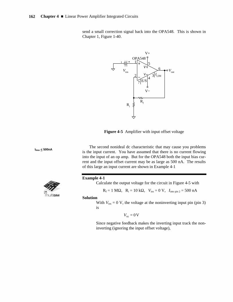
ence in potential between its inputs. However, in reality, the two input transistors cannot be made identically. So there is some small voltage between these two pins. This is the input offset voltage. For the OPA548 its worst case value is ±10 mV.
To figure out the effect this has on the circuit, you can model the in-put offset voltage as a small dc supply in series with the noninverting input. A voltage follower is shown in Figure 4-4. The input offset volt-age drives Vout to equal Vios, instead of 0 V.
ILIM
E/S
1
2 34
7
65
OPA548V+
V−
Vios Vout
Figure 4-4 Voltage follower with input offset voltage
In some critical applications this ±10 mV output dc voltage could cause a problem. However, when you add gain to the circuit, the prob-lem gets worse. Look at Figure 4-5. Ideally, with 0 V in, the output should also be 0 V. But since the input offset voltage is actually be-tween the op amp’s input and common, that voltage looks like an input signal. It is multiplied by the noninverting gain of the circuit.
iosi
fout R
R1 VV
+=
So, for reasonable gains, the output dc voltage could very easily be shifted significant parts of a volt, or more. If this shift in the output dc level causes a problem, you can add a coupling capacitor immediately before the load. Be sure to connect the feedback resistor, Rf, directly to the op amp’s output. You could also add a voltage divider and potenti-ometer to the input, to allow you to tweak the output dc. Or, an integra-tor could be used to automatically sense any dc voltage at the output and
Vios < 10 mV
Chapter 4 n Linear Power Amplifier Integrated Circuits 162
send a small correction signal back into the OPA548. This is shown in Chapter 1, Figure 1-40.
ILIM
E/S
1
2 34
7
65
OPA548V+
V−
Vios Vout
RfRi
Figure 4-5 Amplifier with input offset voltage
The second nonideal dc characteristic that may cause you problems is the input current. You have assumed that there is no current flowing into the input of an op amp. But for the OPA548 both the input bias cur-rent and the input offset current may be as large as 500 nA. The results of this large an input current are shown in Example 4-1
Example 4-1 Calculate the output voltage for the circuit in Figure 4-5 with
Rf = 1 MΩ , Ri = 10 kΩ , Vios = 0 V, Iinto pin 2 = 500 nA
Solution With Vios = 0 V, the voltage at the noninverting input pin (pin 3) is
V0NI =V
Since negative feedback makes the inverting input track the non-inverting (ignoring the input offset voltage),
Ibias < 500nA
Section 4.1 n Power Op Amps 163
V0NIINV ==VV
This means that there is no voltage difference across Ri. So no current flows through it.
A0Ri =I
But, there is 500 nA of bias current flowing into the inverting input pin. It must come from somewhere. Since none of it can come through Ri, it must all come from the output of the op amp, flowing left to right through Rf. This current creates a voltage drop across Rf of
mV500=M1nA500Rf Ω×=V
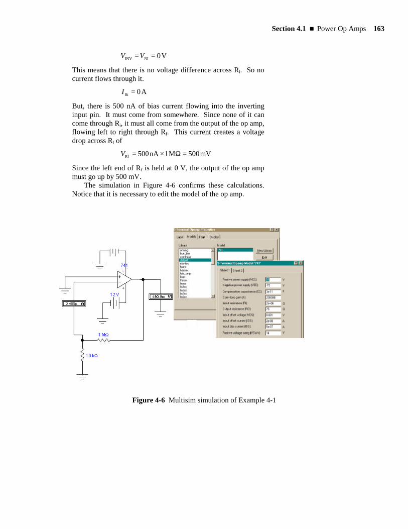
Since the left end of Rf is held at 0 V, the output of the op amp must go up by 500 mV. The simulation in Figure 4-6 confirms these calculations. Notice that it is necessary to edit the model of the op amp.
Figure 4-6 Multisim simulation of Example 4-1
Chapter 4 n Linear Power Amplifier Integrated Circuits 164
Practice: What is the effect on the Vout of lowering the resistors to Ri = 100 Ω , Rf = 10 kΩ
Answer: Vout = 5 mV
To minimize the effect of this unusually large bias current, keep the feedback resistor for the OPA548 as small as practical, typically a few kΩ .
The gain bandwidth product of the OPA548 is typically 1 MHz. This is the same as the 741 small signal amplifier. The gain bandwidth product is defined for small signals (1 Vp). It is
HfAGBW o ×=
where Ao = the amplifier’s closed loop gain fH = the amplifier’s high frequency cutoff, the frequency at
which the gain has dropped to 0.707 Ao.
You may certainly input small signals into the OPA548. So you must be sure to consider the gain bandwidth product. But the main pur-pose of this op amp is to output large signals. For signals above 1 Vp, the op amp’s speed is limited by its slew rate. The slew rate defines how rapidly the output may change.
dtdv
SR out=
For the OPA548 the slew rate is typically 10 V/µs when driving an 8 Ω load with a 50 Vpp signal. If that output is a triangle wave, the slew rate defines the maximum slope of the output. For a rectangular output, the slew rate sets the smallest rise and fall times. But, for a sinusoidal output, you actually have to take the derivative of the signal, and look at that function at its maximum value. The result for a sine wave is called the full power bandwidth. This is the maximum frequency for a large undistorted sine wave output.
pmax p2 V
SRf =
Rf < 10 kΩ
GBW = 1 MHz
SR = 10 V/µs
Section 4.1 n Power Op Amps 165
Example 4-2 An audio amplifier has an input of 300 mVrms and is to deliver 35 W to an 8 Ω speaker. Can the OPA548 be used?
Solution Assuming that the speaker is resistive, and that the signal is a sine wave,
load
2rmsload
load RV
P =
Ω×== 8W35R loadloadrmsload PV
prmsload V7.23V7.16 ==V
pp
load A38
V7.23=
Ω=I
These levels are within the OPA548’s ability.
pmax p2 V
SRf =
fmax ..= × =
10
2 23767 2
Vs
VkHz
p
µπ
Be careful with the units and the powers of ten. The slew rate is specified in V/µs. So the computed answer is 0.0672 MHz. Since the top of the audio band is only 20 kHz, the OPA548 has more than enough slew rate to pass an audio sine wave to the load.
in
out
EV
Ao =
7.55mV300V7.16
rms
rmso ==A

Chapter 4 n Linear Power Amplifier Integrated Circuits 166
Ho fAGBW ×=
MHz1.1kHz207.55 =×=GBW
The OPA548 has high enough voltage, current, and slew rate to serve for this 35 W audio amplifier. But it cannot amplify the high frequency signals enough. That is, its gain bandwidth prod-uct is too small.
Practice: Prove that the amplifier can be built with a small signal 741 op amp amplifier with a gain of 5, followed by the OPA548.
Answer: Vout 741 = 2.12 Vp, SR741 needed = 0.27 V/µs, GBW741 needed = 100 kHz, GBWOPA548 needed = 223 kHz
4.2 Power Calculations In considering the power that a linear power IC delivers to a load, it helps to consider the simplified model shown in Figure 4-7. Of course, the actual circuit is much more complex. But this highlights the key points. The traditional, low power op amp drives two power transistors. The npn transistor, Q1, turns on and sources current from V+ out of the output terminal, through the load, to circuit common. This produces a positive load voltage. On the negative load cycle, the pnp power transis-tor turns on. It sinks current, from circuit common, up through the load, through Q2 and to the negative supply, V− . All of the load current passes through either Q1 and/or Q2.
The power a signal can deliver to the load depends on several fac-tors: the load’s resistance, the op amp’s power supply voltage, and the wave shape. These same factors determine the power that the supply must provide, and the power that the IC must dissipate. In Chapter 3, you saw how to calculate the power resulting from a wide variety of cur-rents and voltages. These are summarized in Table 3-2. The two most prevalent wave shapes, DC and the sinusoid, will be applied to the power amplifier of Figure 4-7. But you can use these same techniques for any signal shape.
DC Signal to the Load When a positive voltage is applied to the load, current flows from V+, through Q1, and to the load. The power that the load dissipates is
Figure 4-7 Simplified model of a power op amp
Q1
Q2
Rload
Section 4.2 n Power Calculations 167
dcloaddcloadload IVP ×=
Assuming that the load is purely resistive, this power equation can be combined with Ohm’s law to give two alternate versions.
load2
dcloadload R×= IP
load
2dcload
load RV
P =
This is the power that the load uses, converting it to heat, light, sound, or motion. Generally, that is the end product and the entire reason for the existence of the electronics. This power is provided by the dc supply. Both V+ and V− are avail-able to allow either positive or negative load voltages. If the load volt-age only goes one direction, then the opposite supply just plays a small, biasing role. It does not deliver any significant power. The power pro-vided by the supply is
P V Isupply supply supply= ×
Since the power supply, Q1, and the load form a series circuit,
dcloadsupply II =
Combining these gives
dcloadsupplysupply IVP ×=
Since the supply voltage is greater than the load voltage, the power supply’s power is always greater than the power delivered to the load. The power that is provided by the supply but is not delivered to the load must be dissipated by Q1 (or Q2 if the output is negative).
loadsupplyIC PPP −=
This power is dissipated as heat in the IC output transistor, raising the temperature of the silicon. You will see in the next section how to pro-vide the correct heat sink to protect the IC.
Example 4-3 Calculate the power delivered to the load, provided by the sup-ply and dissipated by the op amp, for a circuit running from ±12 Vdc, delivering +5 Vdc to a 10 Ω resistive load.
Load power
Supply power
IC power
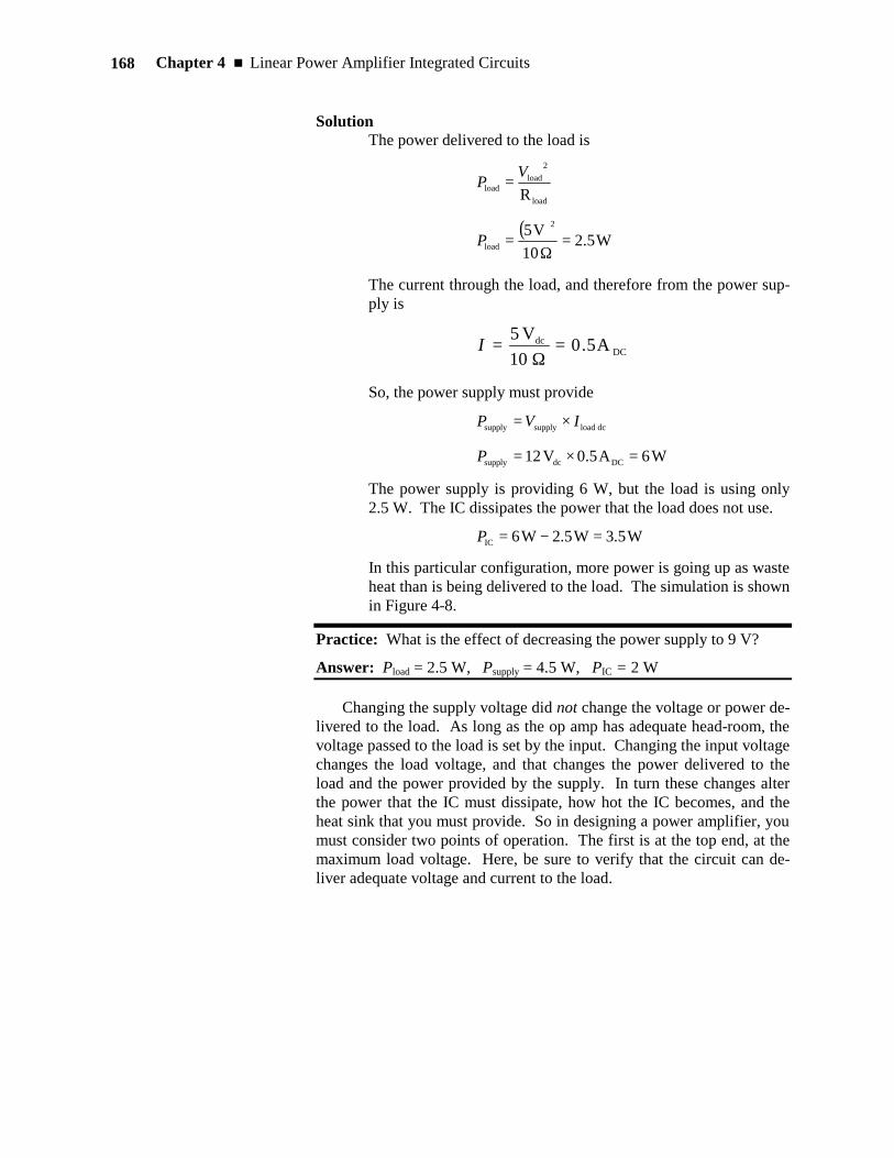
Chapter 4 n Linear Power Amplifier Integrated Circuits 168
Solution The power delivered to the load is
load
2load
load RV
P =
( )W5.2
10V5 2
load =Ω
=P
The current through the load, and therefore from the power sup-ply is
DCdc A5.0
10V5 =Ω
=I
So, the power supply must provide
dcloadsupplysupply IVP ×=
W6A5.0V12 DCdcsupply =×=P
The power supply is providing 6 W, but the load is using only 2.5 W. The IC dissipates the power that the load does not use.
W5.3W5.2W6IC =−=P
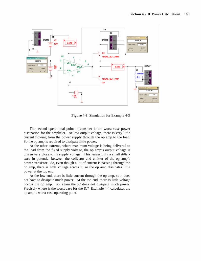
In this particular configuration, more power is going up as waste heat than is being delivered to the load. The simulation is shown in Figure 4-8.
Practice: What is the effect of decreasing the power supply to 9 V?
Answer: Pload = 2.5 W, Psupply = 4.5 W, PIC = 2 W
Changing the supply voltage did not change the voltage or power de-livered to the load. As long as the op amp has adequate head-room, the voltage passed to the load is set by the input. Changing the input voltage changes the load voltage, and that changes the power delivered to the load and the power provided by the supply. In turn these changes alter the power that the IC must dissipate, how hot the IC becomes, and the heat sink that you must provide. So in designing a power amplifier, you must consider two points of operation. The first is at the top end, at the maximum load voltage. Here, be sure to verify that the circuit can de-liver adequate voltage and current to the load.
Section 4.2 n Power Calculations 169
Figure 4-8 Simulation for Example 4-3
The second operational point to consider is the worst case power dissipation for the amplifier. At low output voltage, there is very little current flowing from the power supply through the op amp to the load. So the op amp is required to dissipate little power. At the other extreme, where maximum voltage is being delivered to the load from the fixed supply voltage, the op amp’s output voltage is driven very close to its supply voltage. This leaves only a small differ-ence in potential between the collector and emitter of the op amp’s power transistor. So, even though a lot of current is passing through the op amp, there is little voltage across it, so the op amp dissipates little power at the top end. At the low end, there is little current through the op amp, so it does not have to dissipate much power. At the top end, there is little voltage across the op amp. So, again the IC does not dissipate much power. Precisely where is the worst case for the IC? Example 4-4 calculates the op amp’s worst case operating point.
Chapter 4 n Linear Power Amplifier Integrated Circuits 170
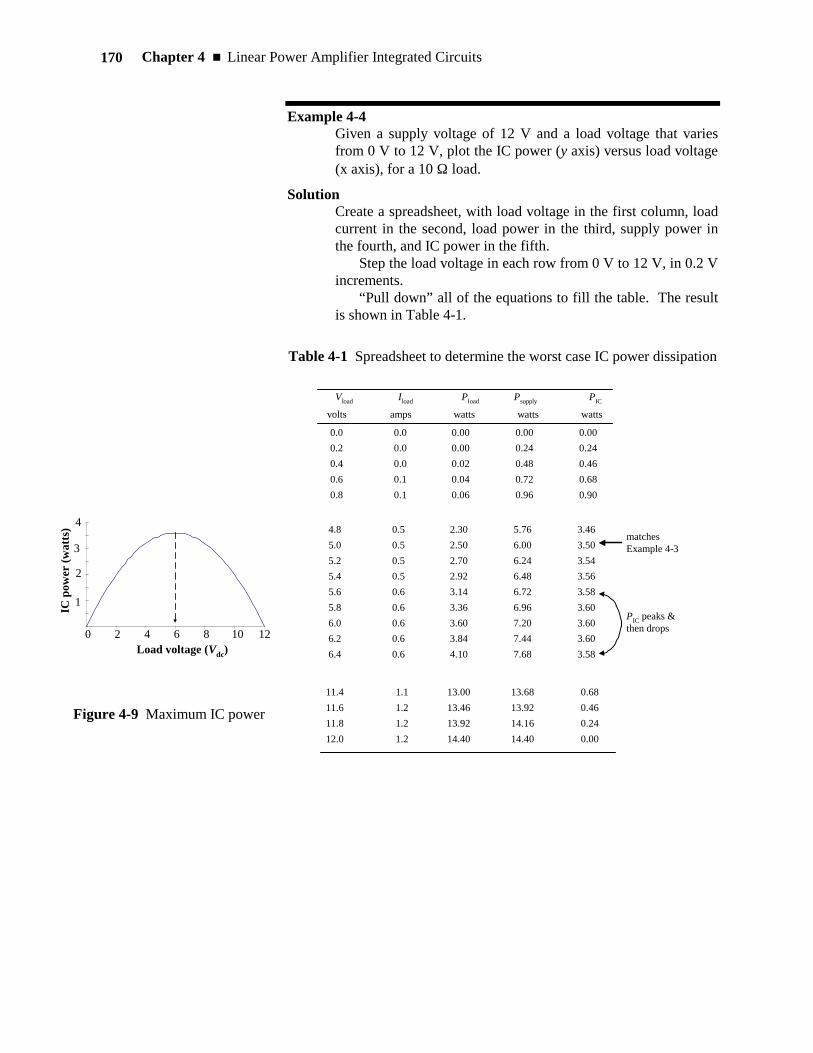
Example 4-4 Given a supply voltage of 12 V and a load voltage that varies from 0 V to 12 V, plot the IC power (y axis) versus load voltage (x axis), for a 10 Ω load.
Solution Create a spreadsheet, with load voltage in the first column, load current in the second, load power in the third, supply power in the fourth, and IC power in the fifth.
Step the load voltage in each row from 0 V to 12 V, in 0.2 V increments.
“Pull down” all of the equations to fill the table. The result is shown in Table 4-1.
Table 4-1 Spreadsheet to determine the worst case IC power dissipation
0.0 0.0 0.00 0.00 0.000.2 0.0 0.00 0.24 0.240.4 0.0 0.02 0.48 0.460.6 0.1 0.04 0.72 0.680.8 0.1 0.06 0.96 0.90
Vload Iload Pload Psupply PIC
volts amps watts watts watts
4.8 0.5 2.30 5.76 3.465.0 0.5 2.50 6.00 3.505.2 0.5 2.70 6.24 3.545.4 0.5 2.92 6.48 3.565.6 0.6 3.14 6.72 3.585.8 0.6 3.36 6.96 3.606.0 0.6 3.60 7.20 3.606.2 0.6 3.84 7.44 3.606.4 0.6 4.10 7.68 3.58
11.4 1.1 13.00 13.68 0.6811.6 1.2 13.46 13.92 0.4611.8 1.2 13.92 14.16 0.2412.0 1.2 14.40 14.40 0.00
matchesExample 4-3
PIC peaks &then drops
2
3
4
0 2 4 6 8 10 12Load voltage (Vdc)
IC p
ower
(wat
ts)
1
Figure 4-9 Maximum IC power
Section 4.2 n Power Calculations 171
There are two points to notice from Table 4-1. The row that starts with Vin = 5 V duplicates the calculations in Example 4-3. This should give you confidence that the calculations in the table are correct. Now, scan down the PIC column. It starts low, grows as Iload increases, peaks, then decreases as the difference between Vsupply and Vload falls. The maximum power that the IC must dissipate occurs when
supplyload 21
VV =
Figure 4-9 is a plot of the data from Table 4-1. It, too, shows a parabola with the IC power peaking when the load voltage is half of the supply voltage.
Practice: Duplicate Table 4-1 and Figure 4-9, with Vsupply = 15 V, and Rload = 5 Ω .
Answer: PIC max = 11.3 W at Vload = 7.5 V
Sinusoidal Signal to the Load The steps you used to determine the effects of a dc signal on the load, the supply, and the power IC can be applied to any wave shape. But the results are different for each different signal. From the calculations in Chapter 3, you saw that the power delivered by a sine wave to a resistive load is
2pp
load
IVP =
In more familiar rms terms, for a sine wave,
2222pppp
load
IVIVP ×==
rmsrmsload IVP =
During the positive half cycle, the upper npn transistor, Q1, inside the op amp turns on, sourcing a half-cycle sine wave current to the load. During the negative half-cycle, Q1 turns off. It passes no current. But Q2 turns on, sinking a half cycle current from the load. So, the positive
Worst case IC power for a DC signal occurs when:
Load power
Chapter 4 n Linear Power Amplifier Integrated Circuits 172
power supply provides current to the load during the positive output half-cycle, and rests during the negative part of the cycle. Similarly, the negative power supply rests during the positive output half-cycle and sinks current during the negative part of the cycle. Again, look back at Table 3-1. The two power supplies must be able to provide Ip. But, a dc ammeter indicates the average value.
load
loadploadpsupplyp R
VII ==
psupplyp
supplydc
II =
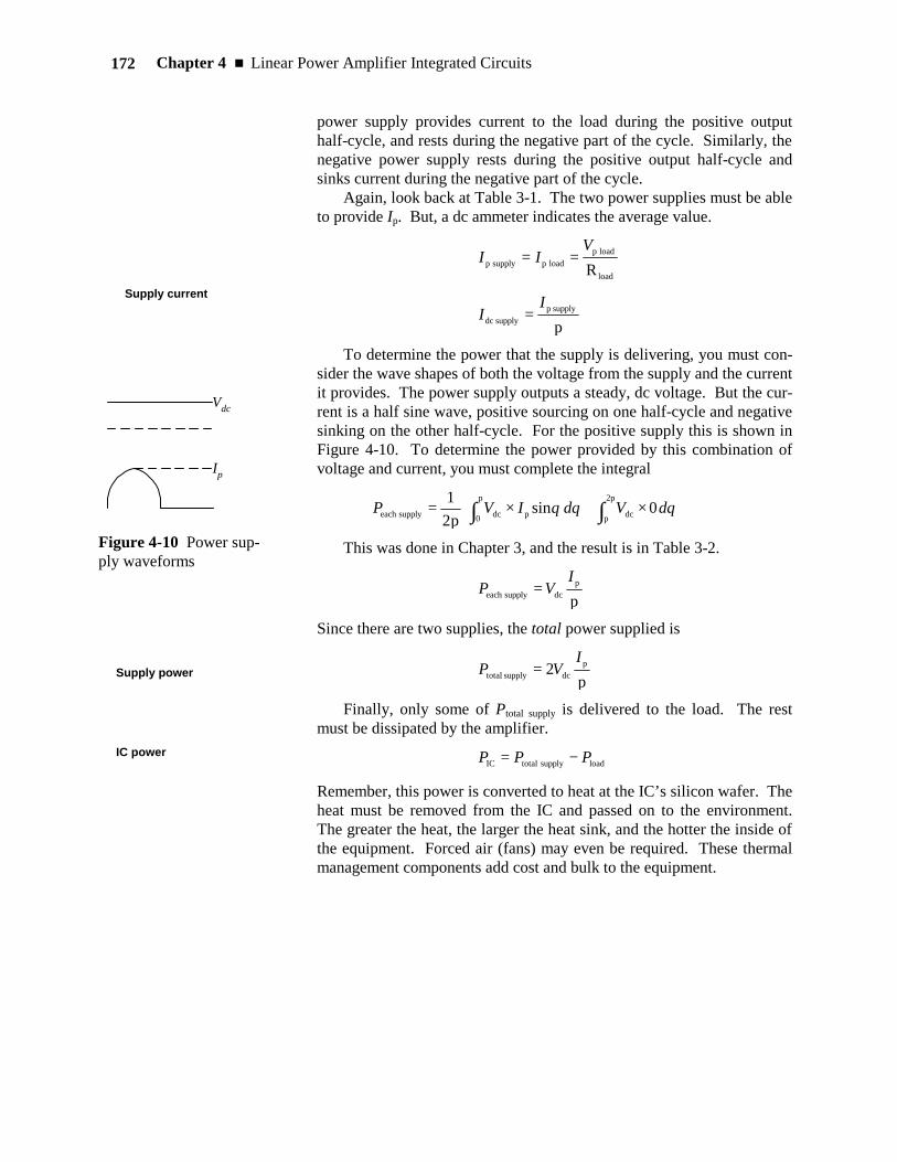
To determine the power that the supply is delivering, you must con-sider the wave shapes of both the voltage from the supply and the current it provides. The power supply outputs a steady, dc voltage. But the cur-rent is a half sine wave, positive sourcing on one half-cycle and negative sinking on the other half-cycle. For the positive supply this is shown in Figure 4-10. To determine the power provided by this combination of voltage and current, you must complete the integral
×+×= ∫ ∫p
0
2p
p dcpdcsupplyeach 0sinp2
1 θθθ dVdIVP
This was done in Chapter 3, and the result is in Table 3-2.
pp
dcsupplyeach
IVP =
Since there are two supplies, the total power supplied is
p2 p
dcsupplytotal
IVP =
Finally, only some of Ptotal supply is delivered to the load. The rest must be dissipated by the amplifier.
loadsupplytotalIC PPP −=
Remember, this power is converted to heat at the IC’s silicon wafer. The heat must be removed from the IC and passed on to the environment. The greater the heat, the larger the heat sink, and the hotter the inside of the equipment. Forced air (fans) may even be required. These thermal management components add cost and bulk to the equipment.
Supply current
Vdc
Ip
Figure 4-10 Power sup-ply waveforms
Supply power
IC power
Section 4.2 n Power Calculations 173
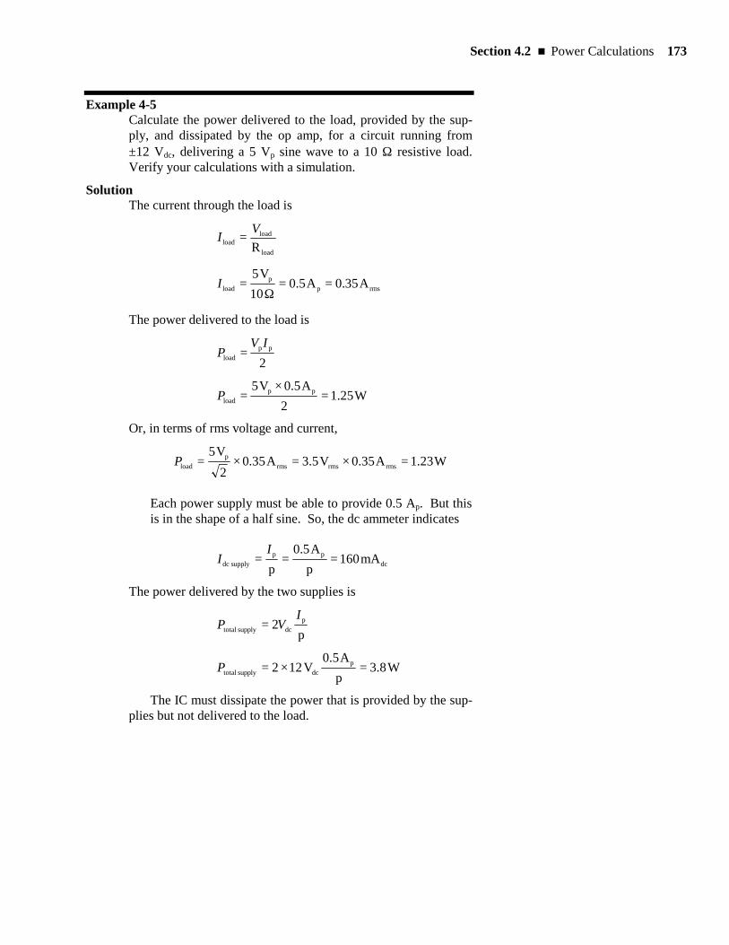
Example 4-5 Calculate the power delivered to the load, provided by the sup-ply, and dissipated by the op amp, for a circuit running from ±12 Vdc, delivering a 5 Vp sine wave to a 10 Ω resistive load. Verify your calculations with a simulation.
Solution The current through the load is
load
loadload R
VI =
rmspp
load A35.0A5.010
V5==
Ω=I
The power delivered to the load is
2pp
load
IVP =
W25.12
A5.0V5 ppload =
×=P
Or, in terms of rms voltage and current,
W23.1A35.0V5.3A35.02
V5rmsrmsrms
pload =×=×=P
Each power supply must be able to provide 0.5 Ap. But this is in the shape of a half sine. So, the dc ammeter indicates
dcpp
supplydc mA160pA5.0
p===
II
The power delivered by the two supplies is
p2 p
dcsupplytotal
IVP =
W8.3pA5.0
V122 pdcsupplytotal =×=P
The IC must dissipate the power that is provided by the sup-plies but not delivered to the load.
Chapter 4 n Linear Power Amplifier Integrated Circuits 174
loadsupplytotalIC PPP −=
W5.2W3.1W8.3IC =−=P
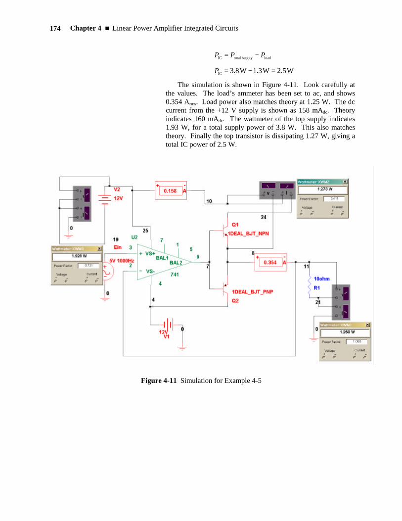
The simulation is shown in Figure 4-11. Look carefully at the values. The load’s ammeter has been set to ac, and shows 0.354 Arms. Load power also matches theory at 1.25 W. The dc current from the +12 V supply is shown as 158 mAdc. Theory indicates 160 mAdc. The wattmeter of the top supply indicates 1.93 W, for a total supply power of 3.8 W. This also matches theory. Finally the top transistor is dissipating 1.27 W, giving a total IC power of 2.5 W.
Figure 4-11 Simulation for Example 4-5
Section 4.2 n Power Calculations 175
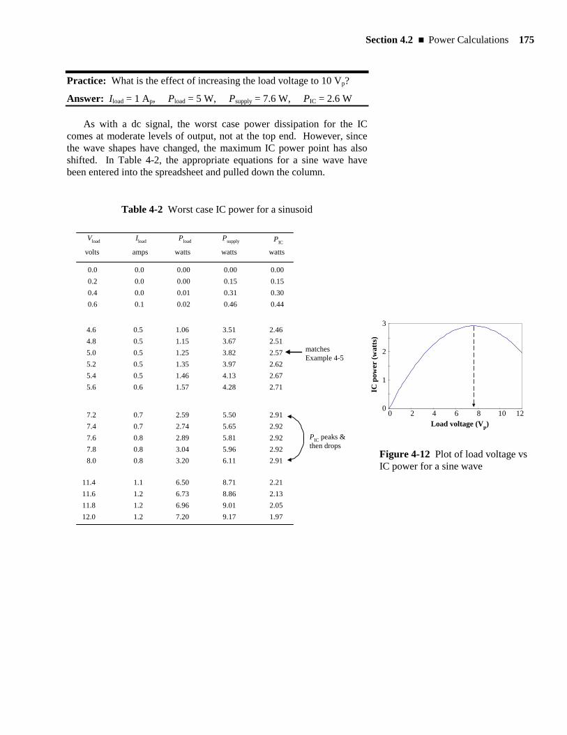
Practice: What is the effect of increasing the load voltage to 10 Vp?
Answer: Iload = 1 Ap, Pload = 5 W, Psupply = 7.6 W, PIC = 2.6 W
As with a dc signal, the worst case power dissipation for the IC comes at moderate levels of output, not at the top end. However, since the wave shapes have changed, the maximum IC power point has also shifted. In Table 4-2, the appropriate equations for a sine wave have been entered into the spreadsheet and pulled down the column.
Table 4-2 Worst case IC power for a sinusoid
0.0 0.0 0.00 0.00 0.000.2 0.0 0.00 0.15 0.150.4 0.0 0.01 0.31 0.300.6 0.1 0.02 0.46 0.44
Vload Iload Pload Psupply PIC
volts amps watts watts watts
4.6 0.5 1.06 3.51 2.464.8 0.5 1.15 3.67 2.515.0 0.5 1.25 3.82 2.575.2 0.5 1.35 3.97 2.625.4 0.5 1.46 4.13 2.675.6 0.6 1.57 4.28 2.71
11.4 1.1 6.50 8.71 2.2111.6 1.2 6.73 8.86 2.1311.8 1.2 6.96 9.01 2.0512.0 1.2 7.20 9.17 1.97
7.2 0.7 2.59 5.50 2.917.4 0.7 2.74 5.65 2.927.6 0.8 2.89 5.81 2.927.8 0.8 3.04 5.96 2.928.0 0.8 3.20 6.11 2.91
matchesExample 4-5
PIC peaks &then drops
Figure 4-12 Plot of load voltage vs IC power for a sine wave
0
1
2
3
0 2 4 6 8 10 12Load voltage (Vp)
IC p
ower
(wat
ts)
Chapter 4 n Linear Power Amplifier Integrated Circuits 176
When the signal applied to the load is steady dc, the IC dissipates maximum power at
supplyDCcaseworstIC@pload 0.5VV =−
But, when the load voltage is a sine wave, the worst case for the IC occurs at a higher point, because the signal only spends a small part of each cycle near the peak.
supplysinecaseworstIC@pload p2
VV =−
For other wave shapes, the worst case occurs at a different place. You have to complete the entire analysis for that particular shape. It will even involve some integrals, since the waveforms you are using are probably not in Table 3-2. Calculate
Vload p, Iload p, Pload, Psupply, PIC
Then use a spreadsheet to investigate the effect of Vload p on PIC.
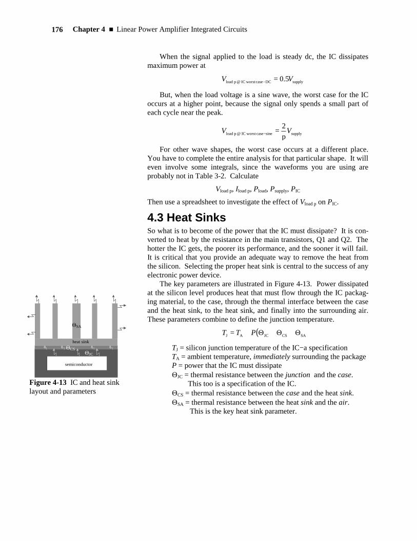
4.3 Heat Sinks So what is to become of the power that the IC must dissipate? It is con-verted to heat by the resistance in the main transistors, Q1 and Q2. The hotter the IC gets, the poorer its performance, and the sooner it will fail. It is critical that you provide an adequate way to remove the heat from the silicon. Selecting the proper heat sink is central to the success of any electronic power device. The key parameters are illustrated in Figure 4-13. Power dissipated at the silicon level produces heat that must flow through the IC packag-ing material, to the case, through the thermal interface between the case and the heat sink, to the heat sink, and finally into the surrounding air. These parameters combine to define the junction temperature.
( )SACSJCAJ Θ+Θ+Θ+= PTT
TJ = silicon junction temperature of the IC− a specification TA = ambient temperature, immediately surrounding the package P = power that the IC must dissipate Θ JC = thermal resistance between the junction and the case.
This too is a specification of the IC. Θ CS = thermal resistance between the case and the heat sink. Θ SA = thermal resistance between the heat sink and the air.
This is the key heat sink parameter.
semiconductor
heat sink
Θ JCΘ CS
Θ SA
Figure 4-13 IC and heat sink layout and parameters
Section 4.3 n Heat Sinks 177
The cooler you can keep the silicon, the longer the IC will run with-out a failure. But for even the worse case conditions, the manufacturer recommends that you must keep
C125J °≤T
Thermal resistance tells you how much hotter the IC gets as heat flows through the packaging material. It is measured in °C of tempera-ture rise for each watt of power dissipated. The thermal resistance, junc-tion-to-case, Θ JC, is set by how the manufacturer packages the silicon wafer. So, it is a specification. For the OPA548 TO220 package, typi-cally
WC
5.2JC
°=Θ
For every watt of power the IC must dissipate in passing a signal to the load, its junction’s temperature goes up 2.5°C as the heat flows out to the case. The interface between the IC’s case and the heat sink is critical. You must not ignore it. The simplest technique is to apply a liberal coat of heat sink grease or compound between the case of the IC and the heat sink. This fills in the surface imperfections and helps the heat tran-sition to the heat sink. This is simple, inexpensive, and effective. But it is messy. Properly applied, a typical value is
WC
2.0CS
°≈Θ grease only
Other forms of thermal adhesives and interface pads are also available. Be sure to verify their thermal resistance before selecting them. In most power ICs the metal package is electrically connected to the most negative potential used by the IC. For the OPA548 the metal tab is tied to V− . If you connect the case directly to the heat sink, then the heat sink, too, is tied to V− . This most certainly can present a shock hazard, and a short circuit with destructive consequences if that heat sink ever touched anything else. So it is often a very good idea to electrically in-sulate the IC package from the heat sink, while keeping as good a ther-mal connection as you can. You can do this by inserting a wafer (often made of mica) between the IC and the heat sink. Be sure to also use an electrically nonconductive thermal grease as well. To provide a solid mechanical structure, either bond the sandwich together with an electri-cally nonconductive glue, or use a nylon bolt, nut, and washers. This
Chapter 4 n Linear Power Amplifier Integrated Circuits 178
provides the electrical insulation you need. But it raises the thermal re-sistance to, typically,
WC
2CS
°≈Θ mica wafer , electrically insulated
The most common way to determine the junction temperature is to measure the case temperature with a temperature sensor. You may do this during prototype testing to assure that the design meets its specifica-tions. Or you may actually build a temperature monitor that measures the case temperature and takes some action to protect the electronics if things get too hot. With the sensor mounted on the heat sink,
( )CSJCCJ Θ+Θ+= PTT
So, measuring the temperature of the case, and knowing the specifica-tions of the IC and the power that it is handling lets you determine the junction’s temperature. This leaves only the heat sink itself. The larger the heat sink, the more fins it contains, and the easier it is for heat to flow through it to the surrounding air. The thermal resistance is inversely proportional to the heat sink’s surface area. A large heat sink has a small thermal resistance and heat flows through it easily, keeping the IC junction cool. This is the only part of the thermal elements over which you have much influ-ence. If you want a different thermal resistance, pick a different heat sink. But be sure it fits into the space you have available. Rearranging the basic thermal equation to solve for the maximum allowable heat sink thermal resistance gives
CSJCcaseworst IC
maxAmaxJmaxSA Θ−Θ−
−=Θ
PTT
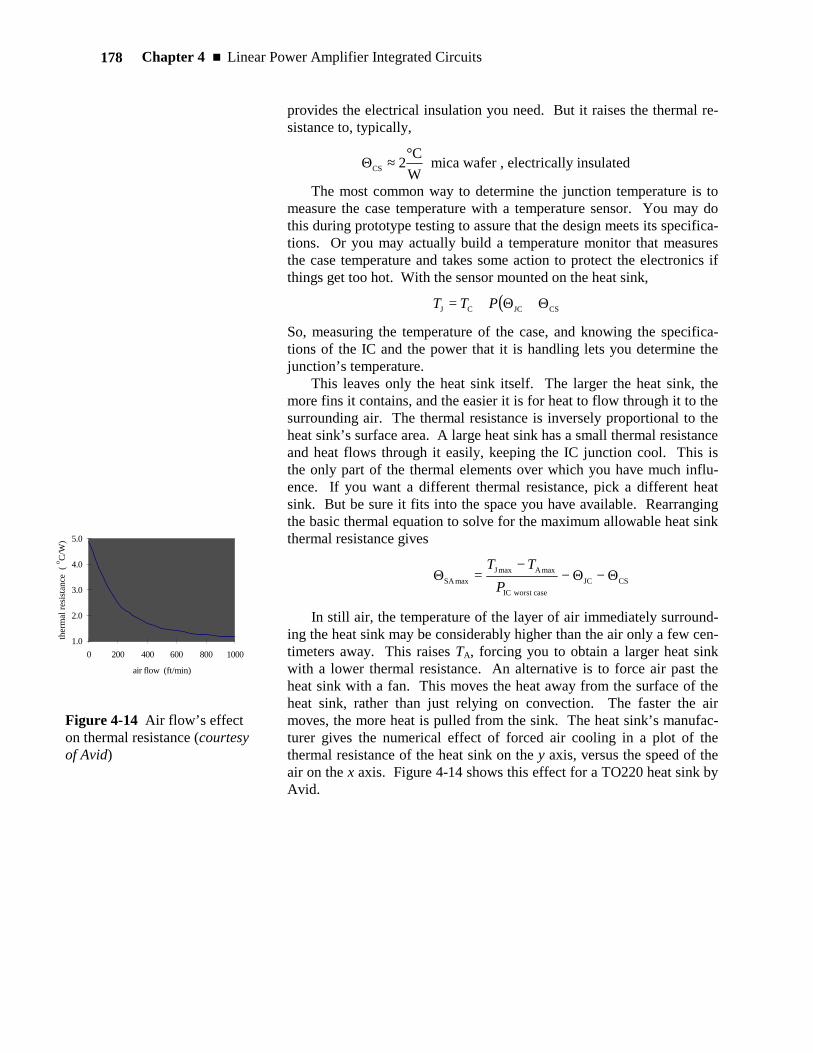
In still air, the temperature of the layer of air immediately surround-ing the heat sink may be considerably higher than the air only a few cen-timeters away. This raises TA, forcing you to obtain a larger heat sink with a lower thermal resistance. An alternative is to force air past the heat sink with a fan. This moves the heat away from the surface of the heat sink, rather than just relying on convection. The faster the air moves, the more heat is pulled from the sink. The heat sink’s manufac-turer gives the numerical effect of forced air cooling in a plot of the thermal resistance of the heat sink on the y axis, versus the speed of the air on the x axis. Figure 4-14 shows this effect for a TO220 heat sink by Avid.
1.0
2.0
3.0
4.0
5.0
0 200 400 600 800 1000
air flow (ft/min)
ther
mal
resi
stan
ce (
o C/W
)
Figure 4-14 Air flow’s effect on thermal resistance (courtesy of Avid)
Section 4.3 n Heat Sinks 179
You may see large areas of a printed circuit board with the copper left in place. The power semiconductor is then bent over and bolted to this expanse of metal. If you have large undedicated areas of your PCB, this may seem like a cheap and easy way to provide a heat sink. How-ever, most printed circuit board material expands seven times more in thickness than it does in the plane of the surface, as it heats up. The co-efficient of expansion for the board is also significantly different from that of the leads, the solder, and any nearby vias. So, as the heat trans-fers to the board, a great deal of force is exerted on the solder joint. Af-ter a surprisingly few cycles of heating and cooling, the leads break free from their solder connections, down inside the board (where you cannot see the break). And worse, the breaks separate when the parts heat up, but when you first turn on the equipment, to try to find the problem, eve-rything is cool, and the broken ends are touching again. Do not use the printed circuit board as a heat sink unless you have PCB material spe-cially designed for that purpose.
Example 4-6 Determine the heat sink’s thermal resistance for the op amp from Example 4-5. Assume an ambient temperature of 40°C.
Solution When picking a heat sink, you must consider the IC’s worst case condition. From Table 4-2 this occurs at
W92.2caseworstC =IP
Solving the fundamental heat sink equation for Θ SA,
CSJCmaxAmaxJ
maxSA Θ−Θ−−
=ΘP
TT
From the specifications for the OPA548, C125maxJ °=T
WC
5.2JC
°=Θ
Since the metal package of the OPA548 is connected to V− , it is wise to isolate the case from the heat sink with a mica wafer.
WC
2CS
°=Θ
Make the substitutions.
Chapter 4 n Linear Power Amplifier Integrated Circuits 180
WC
6.24WC
2WC
5.2W2.92
C40C125maxSA
°=°−°−°−°=Θ
This is the largest thermal resistance that can be used without the IC overheating.
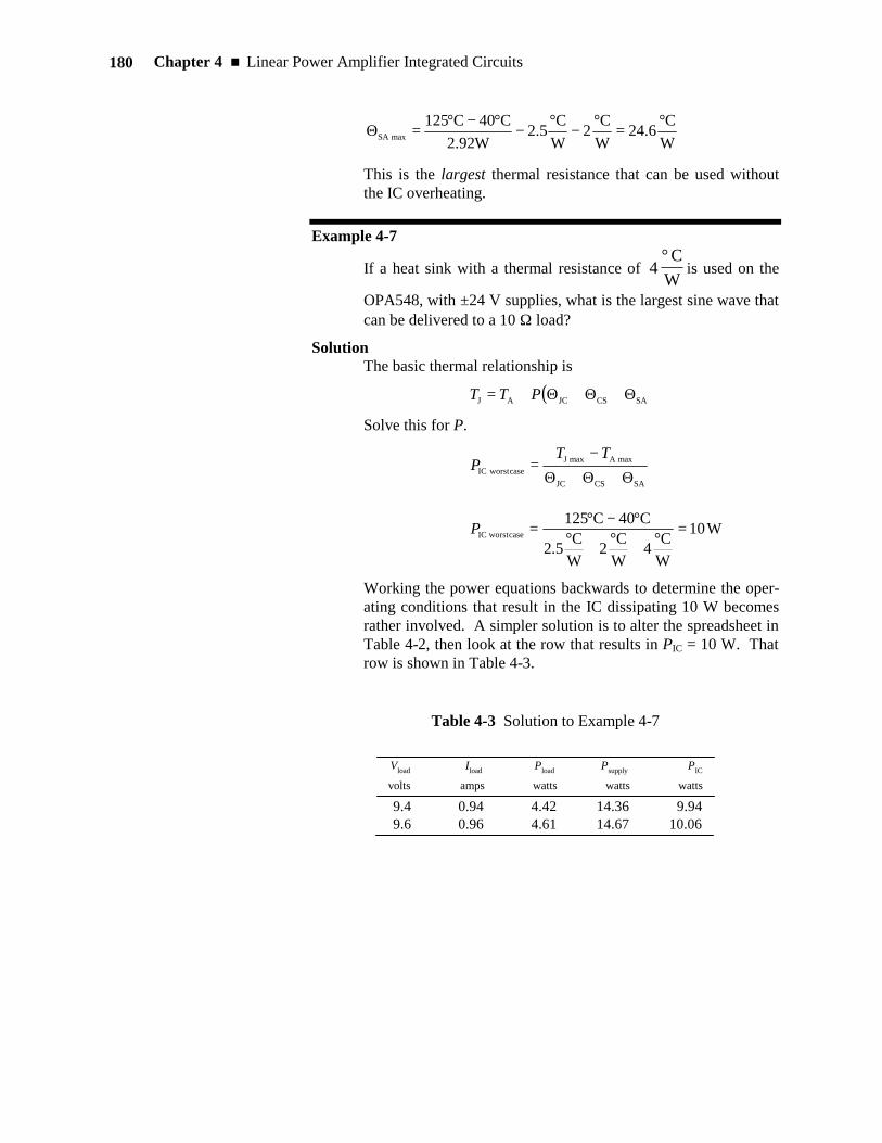
Example 4-7
If a heat sink with a thermal resistance of 4°CW
is used on the
OPA548, with ±24 V supplies, what is the largest sine wave that can be delivered to a 10 Ω load?
Solution The basic thermal relationship is
( )SACSJCAJ Θ+Θ+Θ+= PTT
Solve this for P.
SACSJC
maxAmaxJcaseworstIC Θ+Θ+Θ
−=
TTP
W10
WC4
WC2
WC5.2
C40C125caseworstIC =°+°+°
°−°=P
Working the power equations backwards to determine the oper-ating conditions that result in the IC dissipating 10 W becomes rather involved. A simpler solution is to alter the spreadsheet in Table 4-2, then look at the row that results in PIC = 10 W. That row is shown in Table 4-3.
Table 4-3 Solution to Example 4-7
Vload Iload Pload Psupply PIC
volts amps watts watts watts
9.4 0.94 4.42 14.36 9.949.6 0.96 4.61 14.67 10.06
Section 4.4 n Protecting the OPA548 181
Practice: How much power can the IC dissipate and how much power can be delivered to the load if the heat sink’s thermal resistance is raised
to 8°CW
and the power supplies are lowered to ±18 V?
Answer: PIC worst case = 6.8 W, Pload = 6.5 W
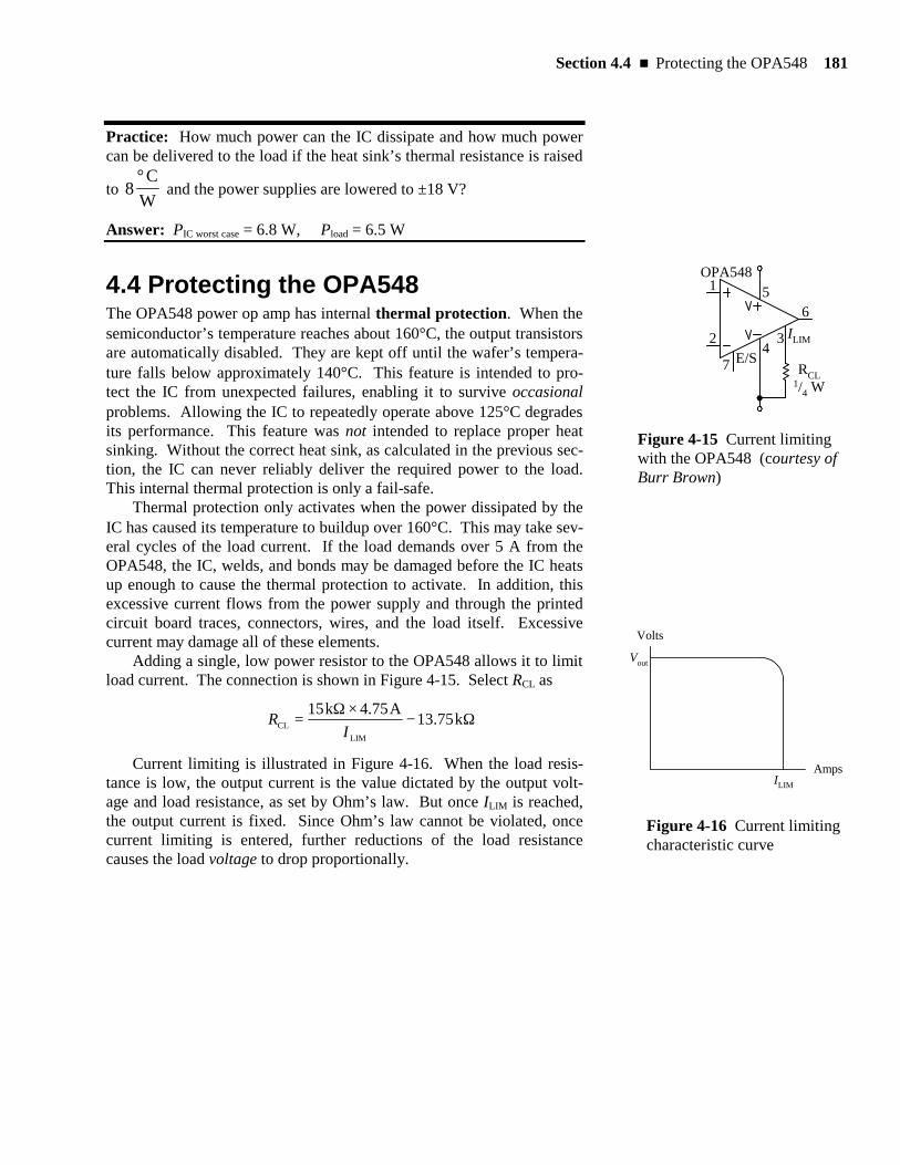
4.4 Protecting the OPA548 The OPA548 power op amp has internal thermal protection. When the semiconductor’s temperature reaches about 160°C, the output transistors are automatically disabled. They are kept off until the wafer’s tempera-ture falls below approximately 140°C. This feature is intended to pro-tect the IC from unexpected failures, enabling it to survive occasional problems. Allowing the IC to repeatedly operate above 125°C degrades its performance. This feature was not intended to replace proper heat sinking. Without the correct heat sink, as calculated in the previous sec-tion, the IC can never reliably deliver the required power to the load. This internal thermal protection is only a fail-safe. Thermal protection only activates when the power dissipated by the IC has caused its temperature to buildup over 160°C. This may take sev-eral cycles of the load current. If the load demands over 5 A from the OPA548, the IC, welds, and bonds may be damaged before the IC heats up enough to cause the thermal protection to activate. In addition, this excessive current flows from the power supply and through the printed circuit board traces, connectors, wires, and the load itself. Excessive current may damage all of these elements. Adding a single, low power resistor to the OPA548 allows it to limit load current. The connection is shown in Figure 4-15. Select RCL as
Ω−×Ω= k75.13A75.4k15
LIMCL I
R
Current limiting is illustrated in Figure 4-16. When the load resis-tance is low, the output current is the value dictated by the output volt-age and load resistance, as set by Ohm’s law. But once ILIM is reached, the output current is fixed. Since Ohm’s law cannot be violated, once current limiting is entered, further reductions of the load resistance causes the load voltage to drop proportionally.
ILIM
E/S
1
2 34
7
65
OPA548
RCL1/4 W
Figure 4-15 Current limiting with the OPA548 (courtesy of Burr Brown)
Volts
Vout
ILIM
Amps
Figure 4-16 Current limiting characteristic curve
Chapter 4 n Linear Power Amplifier Integrated Circuits 182
Current limiting is instantaneous. It affects only those parts of a waveform that result in currents above ILIM. All load currents above ILIM are held at ILIM. This effectively shaves off the peaks. Current limiting only limits the current. It does not prevent the am-plifier from overheating. In fact, should the load be shorted, the load voltage goes to 0 V. This means that the load dissipates no power. The amplifier holds the current to ILIM. The amplifier must now dissipate all of the power being delivered by the supply. If the heat sink is sized for normal operation, it cannot handle this excessive power. The IC’s tem-perature rises. The OPA548 quickly goes into thermal limiting. Without thermal limiting, the IC would burn up. Current limiting does not pro-tect the amplifier from overheating.
Do not try to test current limiting by shorting the load. You will just force the amplifier into thermal shutdown. Instead, raise the output volt-age to its maximum. Then, gradually lower the load resistance until the peaks just begin to flatten. During that flattened part of the output sig-nal, current limiting is being activated. The current limit is
load
peakflattenedmeasuredlim R
VI =
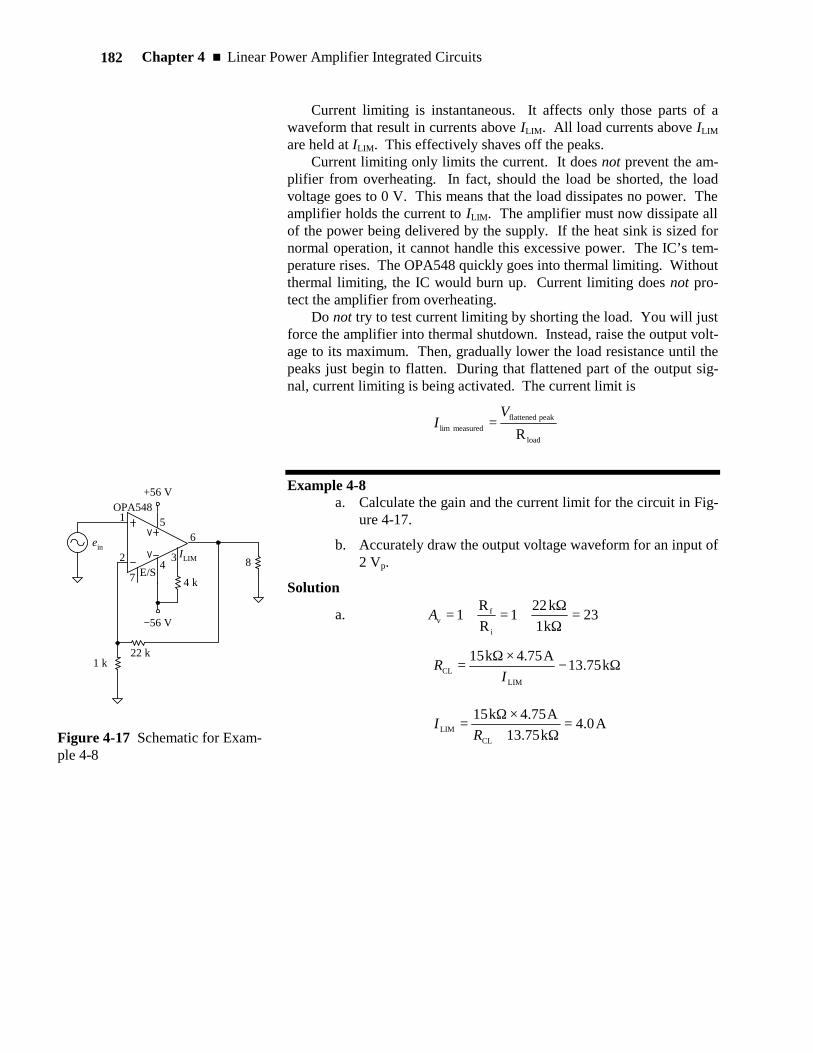
Example 4-8 a. Calculate the gain and the current limit for the circuit in Fig-
ure 4-17.
b. Accurately draw the output voltage waveform for an input of 2 Vp.
Solution
a. 23k1k22
1RR
1i
fv =
ΩΩ+=+=A
Ω−×Ω= k75.13A75.4k15
LIMCL I
R
A0.4k75.13A75.4k15
CLLIM =
Ω+×Ω=
RI
ILIM
E/S
1
2 34
7
65
OPA548
4 k
8
− 56 V
+56 V
22 k1 k
ein
Figure 4-17 Schematic for Exam-ple 4-8
Section 4.5 n Audio Power Parameters 183
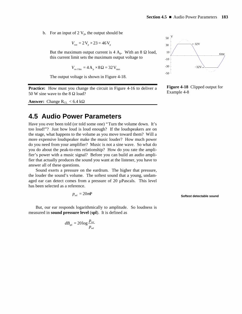
b. For an input of 2 Vp, the output should be
ppout V4623V2 =×=V
But the maximum output current is 4 Ap. With an 8 Ω load, this current limit sets the maximum output voltage to
maxplimIou V328A4 =Ω×=V
The output voltage is shown in Figure 4-18.
Practice: How must you change the circuit in Figure 4-16 to deliver a 50 W sine wave to the 8 Ω load?
Answer: Change RCL < 6.4 kΩ
4.5 Audio Power Parameters Have you ever been told (or told some one) “Turn the volume down. It’s too loud!”? Just how loud is loud enough? If the loudspeakers are on the stage, what happens to the volume as you move toward them? Will a more expensive loudspeaker make the music louder? How much power do you need from your amplifier? Music is not a sine wave. So what do you do about the peak-to-rms relationship? How do you rate the ampli-fier’s power with a music signal? Before you can build an audio ampli-fier that actually produces the sound you want at the listener, you have to answer all of these questions. Sound exerts a pressure on the eardrum. The higher that pressure, the louder the sound’s volume. The softest sound that a young, undam-aged ear can detect comes from a pressure of 20 µPascals. This level has been selected as a reference.
P20ref µ=p
But, our ear responds logarithmically to amplitude. So loudness is
measured in sound pressure level (spl). It is defined as
ref
earspl log20
pp
dB =
-50
-30
-10
10
30
50
time
V
32V
− 32V
Figure 4-18 Clipped output for Example 4-8
Softest detectable sound
Chapter 4 n Linear Power Amplifier Integrated Circuits 184
The softest sound generally detectable produces pear= 20 µP. The thresh-old of hearing, then, is at dBspl threshold = 0 dBspl. A change of 1 dBspl is barely perceivable, although it represents a 26% change in sound pres-sure. Your television remote control alters the volume by about 1.5 dBspl each time you press the volume button. Most people can detect a 3dBspl increase in volume. This requires twice the power from the amplifier. Common volume levels are given in Table 4-4.
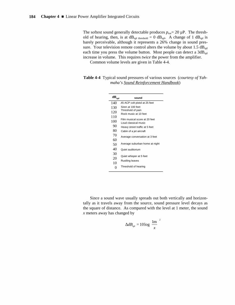
Table 4-4 Typical sound pressures of various sources (courtesy of Yah-maha’s Sound Reinforcement Handbook)
Since a sound wave usually spreads out both vertically and horizon-tally as it travels away from the source, sound pressure level decays as the square of distance. As compared with the level at 1 meter, the sound x meters away has changed by
2
spl
m1log10
=∆
xdB
Threshold of hearing
Rustling leaves
Quiet whisper at 5 feet
Quiet auditorium
Average suburban home at night
Average conversation at 3 feet
Cabin of a jet aircraftHeavy street traffic at 5 feetLoud classical musicFilm musical score at 20 feet
Rock music at 10 feetThreshold of painSiren at 100 feet
.45 ACP colt pistol at 25 feet
dBspl sound
140130120110100 90 80 70 60 50 40 30 20 10 0
Section 4.5 n Audio Power Parameters 185
The square of the argument of a log is the same as twice the log.
=∆
xdB
m1log20spl
Example 4-9 A singer wants to be “loud enough” 8 m from the loudspeakers. The sound from a loudspeaker is rated at 1 m. How loud must the music be 1 m in front of the loudspeaker?
Solution “Loud enough” is interpreted as 90 dBspl. Softer would not be “commanding.” Much louder could be painful to the people closer to the stage.
splm15@spl dB18m8m1
log20 −==∆dB
The sound drops − 18 dBspl as it travels from the loudspeaker to the listener, 8 m away. So, at 1 m from the loudspeaker the sound pressure must be
splsplsplm1@spl dB108dB18dB90 =+=dB
This at the top end of acceptable. Much louder would too loud for the audience close to the loudspeaker.
Practice: A teacher can project a sound of 85 dBspl in a class room. Given that the listener in the back of the room must hear the sound at 70 dBspl, how large can the room be without needing a sound reinforcement system?
Answer: The room may be 5.6 m = 18.5 ft deep.
Loudspeakers convert electrical energy into sound pressure. How effectively they do this is indicated by their rating:
dBspl @ 1 m @ 1 W
The power delivered to the speaker can also be rated in dBW:
dBWP
= 101
log W
Effect of distance on sound
Chapter 4 n Linear Power Amplifier Integrated Circuits 186
This allows the direct conversion between sound pressure level and power delivered to the loudspeaker.
Example 4-10 In Example 4-9, it was decided that 108 dBspl is needed at 1 m in front of the loudspeaker. How much power must be provided by the amplifier if the loudspeaker is rated at 95 dBspl @ 1 m @ 1 W?
Solution When 1 W of power is applied to the loudspeaker, it outputs a 98 dBspl sound. But you want the sound of 108 dBspl.
dB13dB95dB108 =−=∆dB
The power to the loudspeaker must be increased by 13 dBW above 1 W.
dBW13W1
log10 == PdBW
Solve this equation for P.
P = × =1 10 201310W W
Practice: How much power is needed if it is decided to lower the vol-ume at the listener by 6 dBspl?
Answer: The needed power drops to 5 W, a four fold decrease.
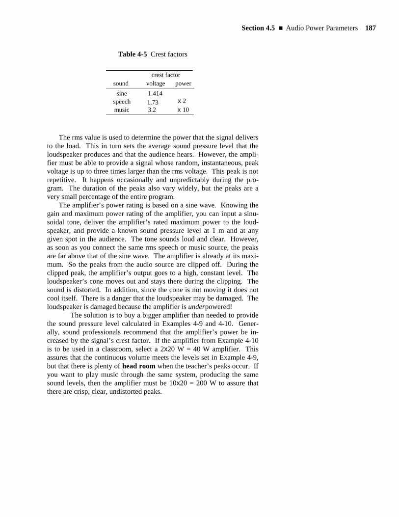
Most testing is done with a sine wave. It is well defined, its shape is not altered by linear components, distortion is easy to detect, and it is commonly available. However, audio program content is not sinusoidal. It is random. That is exactly what makes it interesting to listen to. You have seen repeatedly that the peak of a sine wave is 1.414 times its root mean squared value. And it is this rms value that is used in determining the power delivered to a resistive load (the loudspeaker). The ratio of peak to rms is called the crest factor.
rms
p
VV
factorcrest =
Section 4.5 n Audio Power Parameters 187
Table 4-5 Crest factors
sine 1.414speech 1.73music 3.2
soundcrest factor
voltage power
x 2x 10
The rms value is used to determine the power that the signal delivers to the load. This in turn sets the average sound pressure level that the loudspeaker produces and that the audience hears. However, the ampli-fier must be able to provide a signal whose random, instantaneous, peak voltage is up to three times larger than the rms voltage. This peak is not repetitive. It happens occasionally and unpredictably during the pro-gram. The duration of the peaks also vary widely, but the peaks are a very small percentage of the entire program.
The amplifier’s power rating is based on a sine wave. Knowing the gain and maximum power rating of the amplifier, you can input a sinu-soidal tone, deliver the amplifier’s rated maximum power to the loud-speaker, and provide a known sound pressure level at 1 m and at any given spot in the audience. The tone sounds loud and clear. However, as soon as you connect the same rms speech or music source, the peaks are far above that of the sine wave. The amplifier is already at its maxi-mum. So the peaks from the audio source are clipped off. During the clipped peak, the amplifier’s output goes to a high, constant level. The loudspeaker’s cone moves out and stays there during the clipping. The sound is distorted. In addition, since the cone is not moving it does not cool itself. There is a danger that the loudspeaker may be damaged. The loudspeaker is damaged because the amplifier is underpowered!
The solution is to buy a bigger amplifier than needed to provide the sound pressure level calculated in Examples 4-9 and 4-10. Gener-ally, sound professionals recommend that the amplifier’s power be in-creased by the signal’s crest factor. If the amplifier from Example 4-10 is to be used in a classroom, select a 2x20 W = 40 W amplifier. This assures that the continuous volume meets the levels set in Example 4-9, but that there is plenty of head room when the teacher’s peaks occur. If you want to play music through the same system, producing the same sound levels, then the amplifier must be 10x20 = 200 W to assure that there are crisp, clear, undistorted peaks.
Chapter 4 n Linear Power Amplifier Integrated Circuits 188
The amplitude from the audio signal processor (mixer) is usually measured in dBu.
rms
rms
V775.0log20
vdBu =
The reference voltage of 0.775 Vrms is the amplitude needed to deliver 1 mW into 600 Ω . Signals coming from professional sound reinforce-ment equipment are typically set at about 4 dBu. This translates into 1.23 Vrms. The line out from consumer electronics is usually − 8 dBu, 0.31 Vrms.
Example 4-11 What output voltage and what gain are needed by an amplifier that delivers 20 W to an 8 Ω loudspeaker?
Solution To deliver 20 W to 8 Ω :
PV=
2
R
V P= × = × =R W Vrms20 8 12 7Ω .
From a professional mixer, the line level is 1.23 Vrms, so
in
out
vv
gain =
3.10V23.1V7.12
rms
rms ==gain
Practice: What range of gain must you provide if this amplifier is also to work with consumer electronics.
Answer: 10− 40
Section 4.6 n Low Power Audio Amplifier IC 189
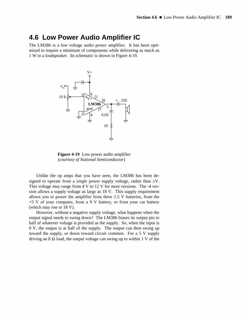
4.6 Low Power Audio Amplifier IC The LM386 is a low voltage audio power amplifier. It has been opti-mized to require a minimum of components while delivering as much as 1 W to a loudspeaker. Its schematic is shown in Figure 4-19.
gnd
V+3
2 4
61
8
57
LM386
V+
ein
10 k
0.05
10
+ 250
Figure 4-19 Low power audio amplifier (courtesy of National Semiconductor)
Unlike the op amps that you have seen, the LM386 has been de-signed to operate from a single power supply voltage, rather than ±V. This voltage may range from 4 V to 12 V for most versions. The -4 ver-sion allows a supply voltage as large as 18 V. This supply requirement allows you to power the amplifier from three 1.5 V batteries, from the +5 V of your computer, from a 9 V battery, or from your car battery (which may rise to 18 V). However, without a negative supply voltage, what happens when the output signal needs to swing down? The LM386 biases its output pin to half of whatever voltage is provided as the supply. So, when the input is 0 V, the output is at half of the supply. The output can then swing up toward the supply, or down toward circuit common. For a 5 V supply driving an 8 Ω load, the output voltage can swing up to within 1 V of the
Chapter 4 n Linear Power Amplifier Integrated Circuits 190
supply, and down to within 1 V of circuit common. As the supply volt-age and resulting load current increase, this saturation level also in-creases. With a 12 V supply and 8 Ω load, the output can swing up to 9.5 V and down to 2.5 V. Refer to the manufacturer’s specifications for a detailed graph of supply voltage versus output peak to peak swing for various loads. The bias voltage at the output must be blocked from the load, while the signal should be passed. That is the role of the 250 µF capacitor just before the loadspeaker. These two form a high pass filter, blocking the dc bias voltage (0 Hz) and passing the signal. The low frequency cut-off is
fCl =
12πR load
For the components in Figure 4-18, signals below 80 Hz are attenuated. If you want to pass more bass, increase this output capacitor. If you are working with speech rather than music, set fl = 300 Hz. This allows you to reduce the size and cost of that capacitor. Another major difference between the LM386 and the general pur-pose op amp is that negative feedback is provided internally by the LM386. Apply the input signal directly to the noninverting pin and tie the inverting input to circuit common. This provides a gain of 20. To invert the signal, apply the signal to the inverting pin and connect the noninverting input to circuit common. This sets the gain to − 20.
With this gain and an output swing of less than 10 Vpp, you must re-strict the input amplitude. The manufacturer rates the maximum input as ±0.4 V. That is the purpose of the input potentiometer. Even though the IC is powered only with a positive voltage, the input may swing both positive and negative 400 mV, without an RC input coupler. Either in-put may be referenced directly to analog common. Each input provides a 50 kΩ resistor to common. Unlike the op amp, the input impedance of the LM386 is not extremely large. It is 50 kΩ . The input potentiometer is set to 10 kΩ to reduce the loading effect of this 50 kΩ input imped-ance.
The internal negative feedback is provided by a 15 kΩ resistor be-tween the output (pin 5) and pin 1. The lower part of the negative feed-back voltage divider is provided internally by a 1.35 kΩ resistor (be-tween pins 1 and 8) and a 150 Ω resistor. The gain is
Low frequency cut-off
Internal gain = 20
Input impedance = 50 kΩ

Section 4.6 n Low Power Audio Amplifier IC 191
Ω+Ω=
− 150k15
281pinR
A
Increase the gain above 20 by placing a resistor and a dc blocking ca-pacitor between pins 1 and 8. This resistor parallels the 1.35 kΩ internal resistor. If you place only a capacitor between pins 1 and 8, the gain rises to 200. Remember to account for the effect of the internal 1.35 kΩ resistor. Select the capacitor’s value so that at the lowest frequency of interest, its reactance is small (1/7) compared to the resistor it affects.
7p2
1
l
RfC >
Example 4-12 Determine the resistor and capacitor you must add between pins 1 and 8 to set the gain at 40, with fl = 80 Hz.
Solution The gain is
Ω+Ω=
− 150k15
281pinR
A
Solve this for Rpin 1-8.
Ω−Ω=− 150k15
281pin AR
Ω=Ω−Ω=− 60015040k15
281pinR
Pick a 620 Ω resistor. The capacitor in series with the 620 Ω resistor should be
F22
7620Hz802
1 µπ
=Ω××>C
Pick a 27 µF capacitor.
Practice: How much gain error would using a 620 Ω resistor produce?
Answer: A = 39 This is an error of 2.5 %.
External gain adjust
Chapter 4 n Linear Power Amplifier Integrated Circuits 192
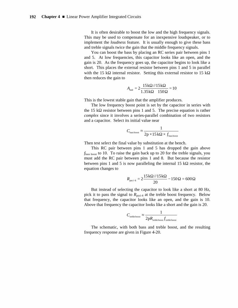
It is often desirable to boost the low and the high frequency signals. This may be used to compensate for an inexpensive loudspeaker, or to implement the loudness feature. It is usually enough to give these bass and treble signals twice the gain that the middle frequency signals. You can boost the bass by placing an RC series pair between pins 1 and 5. At low frequencies, this capacitor looks like an open, and the gain is 20. As the frequency goes up, the capacitor begins to look like a short. This places the external resistor between pins 1 and 5 in parallel with the 15 kΩ internal resistor. Setting this external resistor to 15 kΩ then reduces the gain to
10150k35.1
k15//k152mid =
Ω+ΩΩΩ=A
This is the lowest stable gain that the amplifier produces. The low frequency boost point is set by the capacitor in series with the 15 kΩ resistor between pins 1 and 5. The precise equation is rather complex since it involves a series-parallel combination of two resistors and a capacitor. Select its initial value near
boostbassboostbass k15p2
1f
C×Ω×
≈
Then test select the final value by substitution at the bench. This RC pair between pins 1 and 5 has dropped the gain above fbass boost to 10. To raise the gain back up to 20 for the treble signals, you must add the RC pair between pins 1 and 8. But because the resistor between pins 1 and 5 is now paralleling the internal 15 kΩ resistor, the equation changes to
Ω=Ω−ΩΩ=− 60015020
k15//k15281pinR
But instead of selecting the capacitor to look like a short at 80 Hz, pick it to pass the signal to Rpin1-8 at the treble boost frequency. Below that frequency, the capacitor looks like an open, and the gain is 10. Above that frequency the capacitor looks like a short and the gain is 20.
boosttrebleboosttrebleboosttreble p2
1fR
C ≈
The schematic, with both bass and treble boost, and the resulting frequency response are given in Figure 4-20.
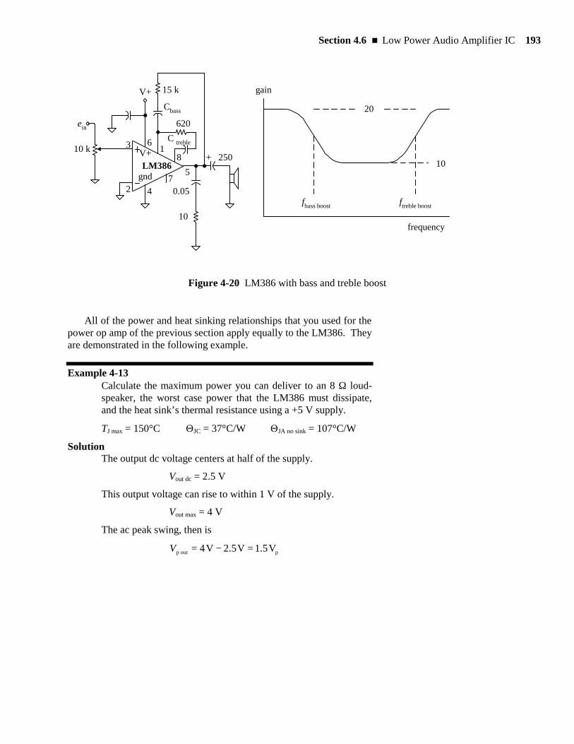
Section 4.6 n Low Power Audio Amplifier IC 193
gnd
V+3
2 4
61
8
57
LM386
V+
ein
10 k
0.05
10
+ 250
620
15 k
Cbass
C treble
gain
frequency
20
10
fbass boost ftreble boost
Figure 4-20 LM386 with bass and treble boost
All of the power and heat sinking relationships that you used for the power op amp of the previous section apply equally to the LM386. They are demonstrated in the following example.
Example 4-13 Calculate the maximum power you can deliver to an 8 Ω loud-speaker, the worst case power that the LM386 must dissipate, and the heat sink’s thermal resistance using a +5 V supply.
TJ max = 150°C Θ JC = 37°C/W Θ JA no sink = 107°C/W
Solution The output dc voltage centers at half of the supply.
Vout dc = 2.5 V
This output voltage can rise to within 1 V of the supply.
Vout max = 4 V
The ac peak swing, then is
poutp V5.1V5.2V4 =−=V
Chapter 4 n Linear Power Amplifier Integrated Circuits 194
Assuming that this signal is a sine wave means that
rmsp
outrms V06.12
V5.1==V
The loudspeaker dissipates
( )load
2rms
load RV
P =
( )mW140
8V1.06 2
rmsload =
Ω=P
In terms of dBW, this is
dBW5.8W1mW140
log10 −==dBW
How loud this sounds depends on the efficiency of the loud-speaker and how close to it you are. Having a +5 V supply sug-gests that this circuit is to be used for a desktop computer moni-tor. So, a distance of 1 m is reasonable. The loudspeaker from earlier examples was rated at
98 dBspl @ 1W @ 1 m
The sound heard, then is
splsplspl dB5.89dB98dBW5.8 =+−=dB
Table 4-4 suggests that this is not quite as loud as heavy street traffic at 5 ft. That certainly should be loud enough for a com-puter monitor on your desk. The worst case output level for the IC (assuming a sine wave) is when the signal is at 63% of the supply voltage. Since the signal swings up and down from 2.5 V, the worst case for the IC is when
pcaseworstp V6.1V5.263.0 =×=V
But the maximum signal is only 1.5 Vp. So the worst case for the IC is at maximum signal. The current from the supply is
Section 4.6 n Low Power Audio Amplifier IC 195
pp
supplyp mA1888
V5.1=
Ω=I
This current flows from the supply, charges the capacitor, and then flows to the load, when the output voltage swings positive. On the negative half-cycle, the IC’s sourcing power transistor turns off, and its sinking transistor is turned on. Current flows from the capacitor, through the IC’s lower transistor to ground, and then up from ground through the load to the negative side of the capacitor. This is how current reverses direction through the load without a negative supply voltage. The key point is that current flows from the supply only dur-ing the positive half-cycle. The power delivered comes from a dc voltage and a half sine current. From Table 3-2 that power is
pp
dcsupply
IVP =
mW299pmA188
V5 pdcsupply ==P
The IC must dissipate the power that is provided by the power supply but is not passed to the load.
loadsupplyIC PPP −=
mW159mW140mW299IC =−=P
The maximum allowable thermal resistance is
PTT AmaxJ
maxJA
−=Θ
For an amplifier that sits on a desk, without forced cooling, it is reasonable to expect that the air next to the enclosed IC gets no hotter than about 50°C.
WC
629W159.0
C50C150maxJA
°=°−°=Θ
This is the maximum allowable thermal resistance. Any value below this will keep the junction temperature below 150°C. The specifications of the thermal resistance for the IC without a heat sink is 107°C/W for the DIP package. So the IC needs no heat sink.
Chapter 4 n Linear Power Amplifier Integrated Circuits 196
Practice: Calculate the maximum power you can deliver to an 8 Ω loudspeaker, the worst case power that the LM386 must dissipate, and the heat sink’s thermal resistance if this amplifier is to be used in a car (+12 V supply).
Answer: Vload p = 3.5 Vp, Pload = 0.77 W, 97 dBspl in the front seat, 91 dBspl in the back seat, Isupply p = 438 mAp, Psupply = 1.7 W, PIC = 0.9 W, Θ JA = 111°C/W.
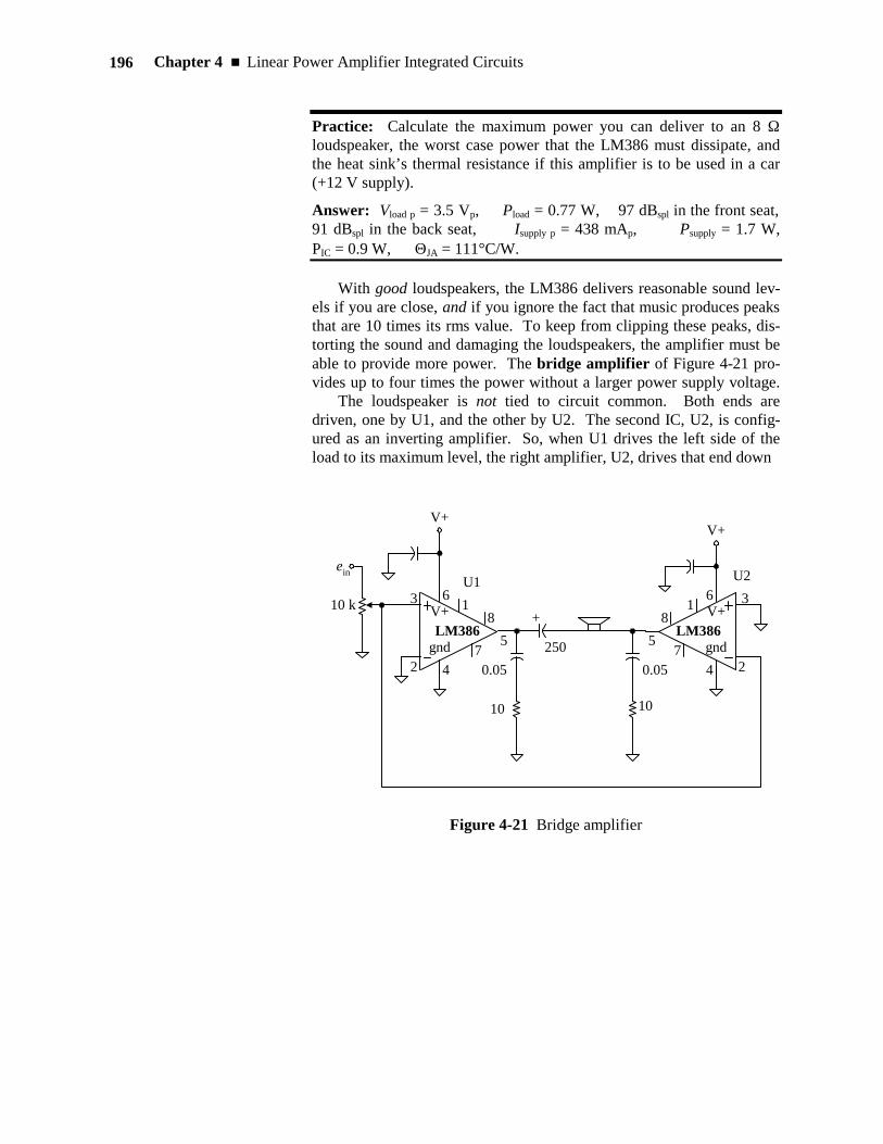
With good loudspeakers, the LM386 delivers reasonable sound lev-els if you are close, and if you ignore the fact that music produces peaks that are 10 times its rms value. To keep from clipping these peaks, dis-torting the sound and damaging the loudspeakers, the amplifier must be able to provide more power. The bridge amplifier of Figure 4-21 pro-vides up to four times the power without a larger power supply voltage. The loudspeaker is not tied to circuit common. Both ends are driven, one by U1, and the other by U2. The second IC, U2, is config-ured as an inverting amplifier. So, when U1 drives the left side of the load to its maximum level, the right amplifier, U2, drives that end down
gnd
V+3
2 4
61
8
57
LM386
V+
ein
10 k
0.05
10
+
250 gnd
V+3
24
61
8
57LM386
0.05
10
V+
U1 U2
Figure 4-21 Bridge amplifier
Section 4.6 n Low Power Audio Amplifier IC 197
just above circuit common. So the total positive peak across the load is almost the supply voltage, not half of the supply as it is when the loud-speaker is tied to common. On the negative half-cycle the left end is driven down near common, while the right end goes close to the supply. However, the current is flowing in the opposite direction. The current has reversed direction without having a negative power supply.
Example 4-14 Calculate the maximum power delivered to an 8 Ω load by a bridged amplifier using two LM386s running from a 5 V supply.
Solution On the positive input peak, U1’s output goes to
V4V1V5maxleft =−=V
U2 drives the right end of the load close to common.
V1minright =V
The peak across the load is
pp V3V1V4 =−=V
Assuming a sine wave,
rmsp
rms V1.22
V3==V
The power delivered to the load is
( )mW551
8V1.2 2
rmsload =
Ω=P
Practice: Calculate the maximum power delivered to an 8 Ω load by a bridged amplifier using two LM386s running from a 12 V supply. At this supply level, there is a 2.5 V saturation.
Answer: 3 W
Chapter 4 n Linear Power Amplifier Integrated Circuits 198
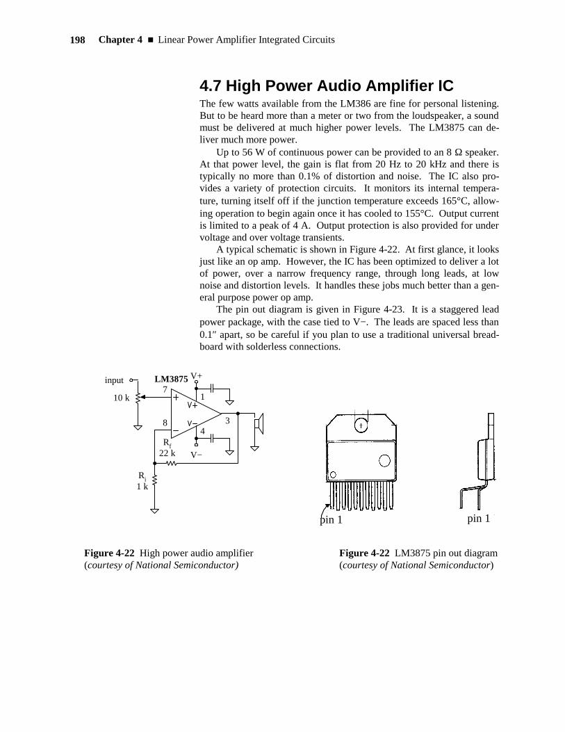
4.7 High Power Audio Amplifier IC The few watts available from the LM386 are fine for personal listening. But to be heard more than a meter or two from the loudspeaker, a sound must be delivered at much higher power levels. The LM3875 can de-liver much more power.
Up to 56 W of continuous power can be provided to an 8 Ω speaker. At that power level, the gain is flat from 20 Hz to 20 kHz and there is typically no more than 0.1% of distortion and noise. The IC also pro-vides a variety of protection circuits. It monitors its internal tempera-ture, turning itself off if the junction temperature exceeds 165°C, allow-ing operation to begin again once it has cooled to 155°C. Output current is limited to a peak of 4 A. Output protection is also provided for under voltage and over voltage transients.
A typical schematic is shown in Figure 4-22. At first glance, it looks just like an op amp. However, the IC has been optimized to deliver a lot of power, over a narrow frequency range, through long leads, at low noise and distortion levels. It handles these jobs much better than a gen-eral purpose power op amp.
The pin out diagram is given in Figure 4-23. It is a staggered lead power package, with the case tied to V− . The leads are spaced less than 0.1″ apart, so be careful if you plan to use a traditional universal bread-board with solderless connections.
input
10 k
Rf22 k
Ri1 k
V−
V+
1
34
7
8
LM3875
pin 1 pin 1
Figure 4-22 LM3875 pin out diagram (courtesy of National Semiconductor)
Figure 4-22 High power audio amplifier (courtesy of National Semiconductor)
Section 4.7 n High Power Audio Amplifier IC 199
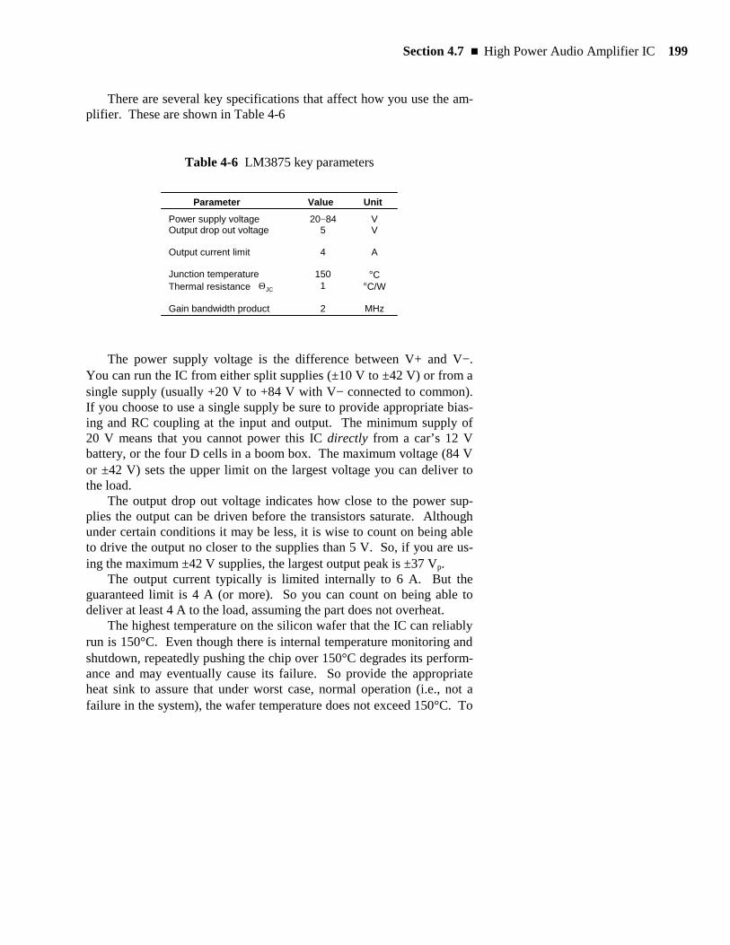
There are several key specifications that affect how you use the am-plifier. These are shown in Table 4-6
Table 4-6 LM3875 key parameters
Power supply voltage 20− 84 VOutput drop out voltage 5 V
Output current limit 4 A
Junction temperature 150 °CThermal resistance Θ JC 1 °C/W
Gain bandwidth product 2 MHz
Parameter Value Unit
The power supply voltage is the difference between V+ and V− . You can run the IC from either split supplies (±10 V to ±42 V) or from a single supply (usually +20 V to +84 V with V− connected to common). If you choose to use a single supply be sure to provide appropriate bias-ing and RC coupling at the input and output. The minimum supply of 20 V means that you cannot power this IC directly from a car’s 12 V battery, or the four D cells in a boom box. The maximum voltage (84 V or ±42 V) sets the upper limit on the largest voltage you can deliver to the load. The output drop out voltage indicates how close to the power sup-plies the output can be driven before the transistors saturate. Although under certain conditions it may be less, it is wise to count on being able to drive the output no closer to the supplies than 5 V. So, if you are us-ing the maximum ±42 V supplies, the largest output peak is ±37 Vp. The output current typically is limited internally to 6 A. But the guaranteed limit is 4 A (or more). So you can count on being able to deliver at least 4 A to the load, assuming the part does not overheat. The highest temperature on the silicon wafer that the IC can reliably run is 150°C. Even though there is internal temperature monitoring and shutdown, repeatedly pushing the chip over 150°C degrades its perform-ance and may eventually cause its failure. So provide the appropriate heat sink to assure that under worst case, normal operation (i.e., not a failure in the system), the wafer temperature does not exceed 150°C. To
Chapter 4 n Linear Power Amplifier Integrated Circuits 200
determine this heat sink, you need to know the thermal resistance be-tween the junction and the case, Θ JC. It is no larger than 1°C/W. Finally, the maximum closed loop gain is determined by the highest frequency to be amplified and the IC’s gain bandwidth product. Al-though the GBW is typically 8 MHz, the worst case guaranteed value is 2 MHz. So, for a sine wave at the upper end of the audio range, 20 kHz, you can have a closed loop gain of 100. But, remember, at that fre-quency, the actual gain has dropped by 0.707 (− 3 dB). In addition to the limitations dictated by these specifications, there are several precautions you must observe to assure that your amplifier works well. Review Chapter 2 on the proper methods to breadboard and to lay out a printed circuit board for a power amplifier. All of the tech-niques and warnings presented there apply when you are using the LM3875. Be sure to:
• Keep the input and the output connections well separated.
• Rigorously decouple each power supply pin, as close to that pin as possible with a 10 µF electrolytic and a 0.1 µF film capacitor.
• Connect the speaker return directly to the analog common in its own separate lead, not back to the amplifier board’s common.
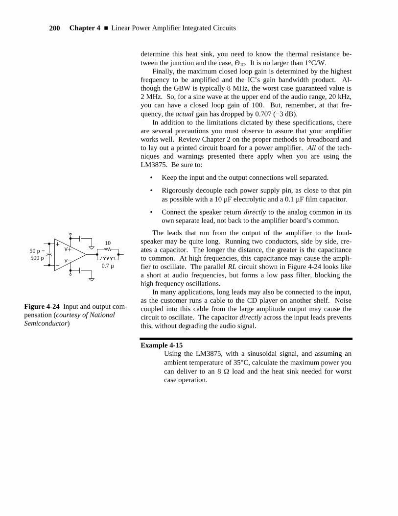
The leads that run from the output of the amplifier to the loud-speaker may be quite long. Running two conductors, side by side, cre-ates a capacitor. The longer the distance, the greater is the capacitance to common. At high frequencies, this capacitance may cause the ampli-fier to oscillate. The parallel RL circuit shown in Figure 4-24 looks like a short at audio frequencies, but forms a low pass filter, blocking the high frequency oscillations. In many applications, long leads may also be connected to the input, as the customer runs a cable to the CD player on another shelf. Noise coupled into this cable from the large amplitude output may cause the circuit to oscillate. The capacitor directly across the input leads prevents this, without degrading the audio signal.
Example 4-15 Using the LM3875, with a sinusoidal signal, and assuming an ambient temperature of 35°C, calculate the maximum power you can deliver to an 8 Ω load and the heat sink needed for worst case operation.
50 p −500 p
10
0.7 µ
Figure 4-24 Input and output com-pensation (courtesy of National Semiconductor)
Section 4.7 n High Power Audio Amplifier IC 201
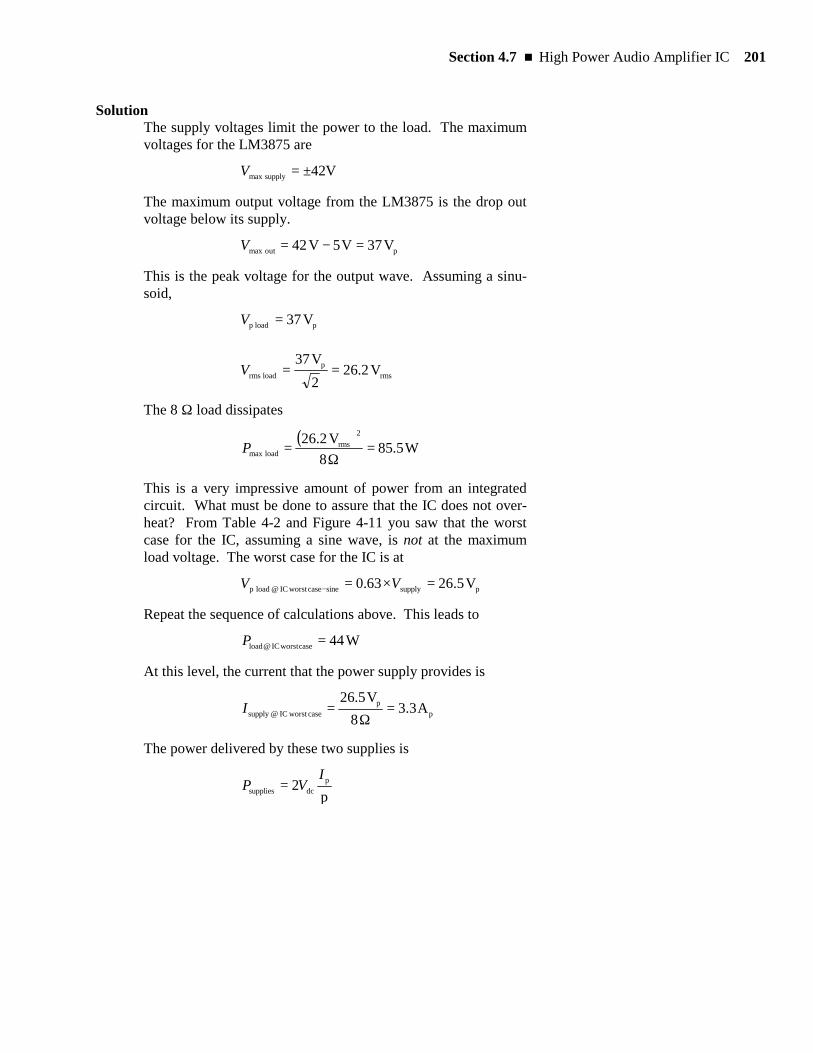
Solution The supply voltages limit the power to the load. The maximum voltages for the LM3875 are
V42supplymax ±=V
The maximum output voltage from the LM3875 is the drop out voltage below its supply.
poutmax V37V5V42 =−=V
This is the peak voltage for the output wave. Assuming a sinu-soid,
ploadp V37=V
rmsp
loadrms V2.262
V37==V
The 8 Ω load dissipates
( )W5.85
8V2.26 2
rmsloadmax =
Ω=P
This is a very impressive amount of power from an integrated circuit. What must be done to assure that the IC does not over-heat? From Table 4-2 and Figure 4-11 you saw that the worst case for the IC, assuming a sine wave, is not at the maximum load voltage. The worst case for the IC is at
psupplysinecaseworstIC@loadp V5.2663.0 =×=− VV
Repeat the sequence of calculations above. This leads to
W44caseworstIC@load =P
At this level, the current that the power supply provides is
pp
caseworstIC@supply A3.38
V5.26=
Ω=I
The power delivered by these two supplies is
p2 p
dcsupplies
IVP =
Chapter 4 n Linear Power Amplifier Integrated Circuits 202
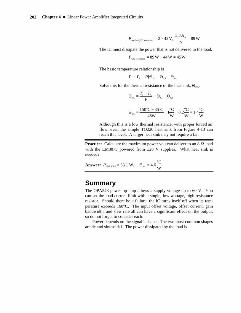
W89pA3.3
V422 pdccaseworstIC@supplies =×=P
The IC must dissipate the power that is not delivered to the load.
W45W44W89caseworst@IC =−=P
The basic temperature relationship is
( )SACSJCAJ Θ+Θ+Θ+= PTT
Solve this for the thermal resistance of the heat sink, Θ SA.
CSJCAJ
SA Θ−Θ−−=ΘP
TT
WC
4.1WC
2.0WC
1W45
C35C150SA
°=°−°−°−°=Θ
Although this is a low thermal resistance, with proper forced air flow, even the simple TO220 heat sink from Figure 4-13 can reach this level. A larger heat sink may not require a fan.
Practice: Calculate the maximum power you can deliver to an 8 Ω load with the LM3875 powered from ±28 V supplies. What heat sink is needed?
Answer: Pload max = 33.1 W, WC
6.4SA
°=Θ
Summary The OPA548 power op amp allows a supply voltage up to 60 V. You can set the load current limit with a single, low wattage, high resistance resistor. Should there be a failure, the IC turns itself off when its tem-perature exceeds 160°C. The input offset voltage, offset current, gain bandwidth, and slew rate all can have a significant effect on the output, so do not forget to consider each. Power depends on the signal’s shape. The two most common shapes are dc and sinusoidal. The power dissipated by the load is
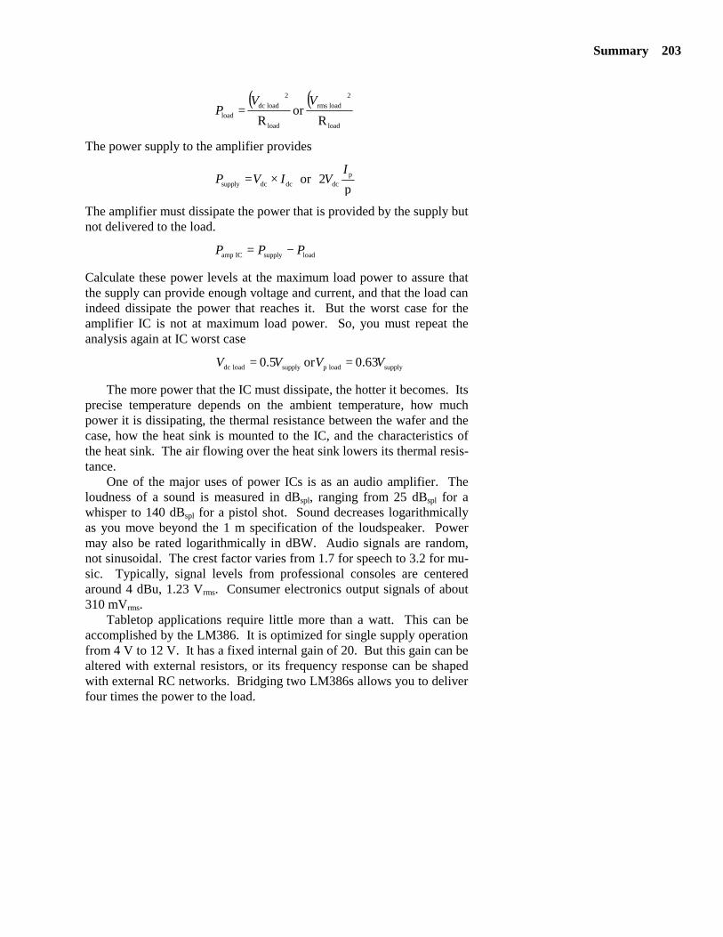
Summary 203
( ) ( )load
2loadrms
load
2loaddc
load Ror
RVV
P =
The power supply to the amplifier provides
p2or p
dcdcdcsupply
IVIVP ×=
The amplifier must dissipate the power that is provided by the supply but not delivered to the load.
loadsupplyICamp PPP −=
Calculate these power levels at the maximum load power to assure that the supply can provide enough voltage and current, and that the load can indeed dissipate the power that reaches it. But the worst case for the amplifier IC is not at maximum load power. So, you must repeat the analysis again at IC worst case
supplyloadpsupplyloaddc 63.0or5.0 VVVV ==
The more power that the IC must dissipate, the hotter it becomes. Its precise temperature depends on the ambient temperature, how much power it is dissipating, the thermal resistance between the wafer and the case, how the heat sink is mounted to the IC, and the characteristics of the heat sink. The air flowing over the heat sink lowers its thermal resis-tance. One of the major uses of power ICs is as an audio amplifier. The loudness of a sound is measured in dBspl, ranging from 25 dBspl for a whisper to 140 dBspl for a pistol shot. Sound decreases logarithmically as you move beyond the 1 m specification of the loudspeaker. Power may also be rated logarithmically in dBW. Audio signals are random, not sinusoidal. The crest factor varies from 1.7 for speech to 3.2 for mu-sic. Typically, signal levels from professional consoles are centered around 4 dBu, 1.23 Vrms. Consumer electronics output signals of about 310 mVrms. Tabletop applications require little more than a watt. This can be accomplished by the LM386. It is optimized for single supply operation from 4 V to 12 V. It has a fixed internal gain of 20. But this gain can be altered with external resistors, or its frequency response can be shaped with external RC networks. Bridging two LM386s allows you to deliver four times the power to the load.
Chapter 4 n Linear Power Amplifier Integrated Circuits 204
For more power (over 50 W), consider the LM3875. It is configured very much like an op amp. It may be run from a single supply or from split supplies (20 V to 80 V). The load current is internally limited to at least 4 A, and the junction temperature is monitored and automatically limited. The power ICs that you have seen in this chapter are convenient. But convenience is purchased at the expense of flexibility. Different voltage and power levels, increased frequency performance, custom cur-rent foldback, current output (to drive particularly low load resistances), and load power in the hundreds of watts require that you design the am-plifier yourself. In Chapter 5 you will build on the fundamentals intro-duced here to construct custom MOSFET linear power amplifiers.
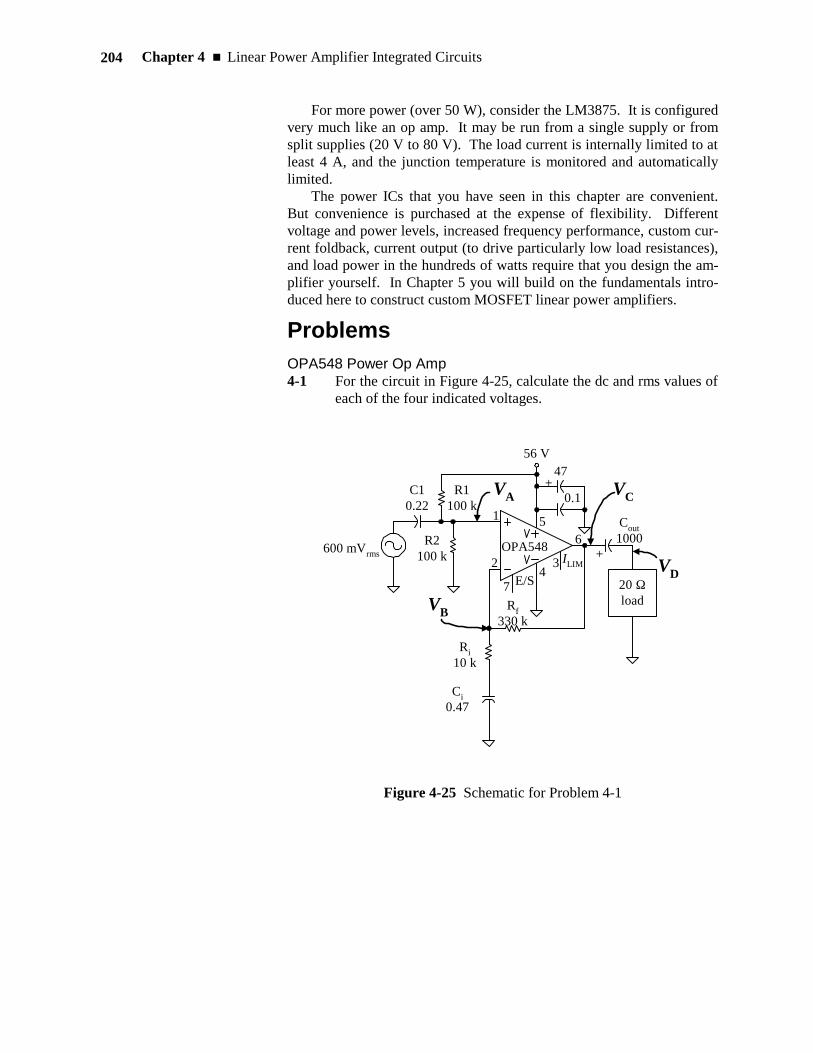
Problems OPA548 Power Op Amp 4-1 For the circuit in Figure 4-25, calculate the dc and rms values of
each of the four indicated voltages.
ILIM
E/S
1
2 34
7
65
OPA548
20 Ωload
56 V
R1100 k
R2100 k
C10.22
Rf330 k
Ri10 k
Ci0.47
47+
0.1
+
Cout1000
600 mVrms
VA
VB
VC
VD
Figure 4-25 Schematic for Problem 4-1

Problems 205
4-2 Explain the purpose of each of the following components in Fig-ure 4-25: C1, R1 R2, Ci, and Cout
4-3 The nonideal input offset voltage, bias currents, and offset cur-rents are shown in Figure 4-26. Calculate the indicated voltages and currents. Hint: do the calculations in the indicated order.
ILIM
E/S
1
2 34
7
65
OPA548
20 Ωload
+28 V
Rf330 k
Ri10 k
47
0.1
+
10 mVdc
VA
VB
− 28 V
47
0.1
750 nA
250 nA
IA IB
IC
+
Figure 4-26 Schematic for Problem 4-3
4-4 For the circuit in Figure 4-26, if the 10 mVdc offset voltage source is replaced with a 500 mVrms sinusoid,
a. calculate the high frequency cut-off, fH.
b. What is the output amplitude at fH?
c. Is the output signal distorted by the op amp’s slew rate limit? Prove your answer with a calculation.
d. Can a larger input be applied without distorting the output? Explain your answer with calculations.
Chapter 4 n Linear Power Amplifier Integrated Circuits 206
Power Calculations 4-5 An OPA548 is powered from ±28 V, and is driving a 20 Ω resis-
tive load. For a dc input signal, calculate the following at the maximum load power: Pload, Psupply, PIC.
4-6 Repeat Problem 4-5 at the operating point that causes the IC to dissipate maximum power.
4-7 An OPA548 is powered from ±28 V, and is driving a 20 Ω resis-tive load. For a sinusoidal input signal, calculate the following at the maximum load power: Pload, Pboth supplies, PIC.
4-8 Repeat Problem 4-7 at the operating point that causes the IC to dissipate maximum power.
Heat Sinks 4-9 For the following conditions, determine the OPA548’s junction
temperature:
TA = 35°C, PIC = 10 W, WC
4SA
°=Θ , mica wafer
4-10 For the following conditions, calculate the largest acceptable heat sink thermal resistance for a OPA548.
TA = 35°C, PIC = 10 W, mica wafer
4-11 Locate the specifications for a heat sink that full-fills the re-quirements from Problem 4-10, in still air.
4-12 For the following conditions, calculate the maximum power that can be delivered by a sinusoidal signal: to a 20 Ω load, by a OPA548 and a sinusoidal signal from ±28 V supplies.
TA = 35°C, mica wafer, Rload = 20 Ω , OPA548, Vsupply = ±28 V
Audio Power Parameters 4-13 A sound level meter indicates 105 dBspl.
a. How loud is that in qualitative terms? b. How much pressure is being exerted on the eardrum? c. If you wanted to lower the volume to that of average conver-
sation, how many TV remote clicks does it take?
4-14 If the 105 dBspl is measured 20 feet from the loudspeaker, how far must you move from the loudspeaker for the sound to drop to 70 dBspl?
Problems 207
4-15 The loudspeaker producing the 105 dBspl at 20 feet is rated at 90 dBspl @ 1 W @ 1m. How much power must you provide to the loudspeaker to produce the 105 dBspl at 20 feet?
4-16 An audio amplifier is capable of outputting 24 Vp. How much music power can be delivered to an 8 Ω loudspeaker without distorting the sound?
4-17 To deliver 10 W to a 4 Ω loudspeaker, how much gain must the audio amplifier have if it is to be driven from a typical consumer electronics signal?
Low Power Audio Amplifier IC 4-18 Design an amplifier circuit using the LM386 to run from a 5 V
supply, driving a 4 Ω loudspeaker. Select all components. De-termine the heat sink’s thermal resistance assuming an ambient temperature of 35°C.
4-19 Repeat Problem 4-18 using a 12 V power supply.
4-20 Alter your design from problem 4-18 to allow a 20 mVrms input to produce 0.5 W into the 4 Ω loudspeaker.
High Power Audio Amplifier IC 4-21 Design an amplifier circuit using the LM3875 to run from ±28 V
supply, driving an 8 Ω loudspeaker. Assume that an input signal of 500 mVrms produces the maximum output power. Select all components. Determine the heat sink’s thermal resistance as-suming an ambient temperature of 40°C.
4-22 Complete the design of the bridge amplifier shown in Figure 4-27. Set the gain to allow a 500 mVrms signal to produce the maximum output power. Calculate the power delivered to the load and the heat sinks’ thermal resistance assuming an ambient temperature of 40°C.
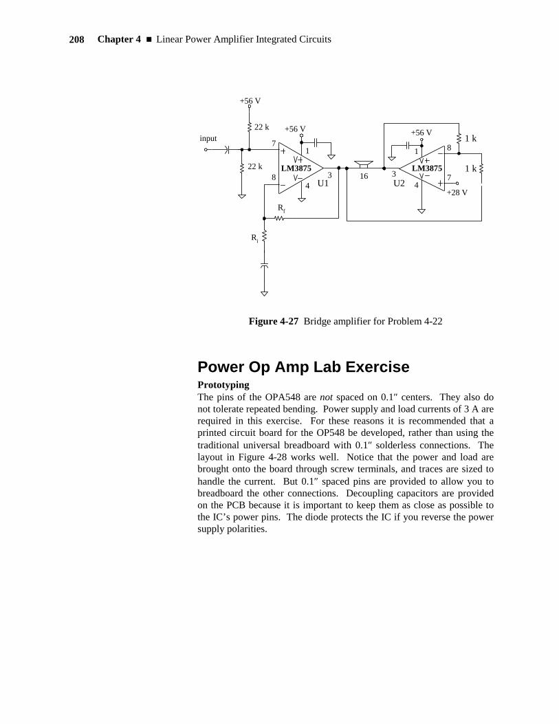
Chapter 4 n Linear Power Amplifier Integrated Circuits 208
Rf
Ri
+56 V
1
34
7
8LM3875 LM3875
+56 V
734
1 8
16
1 k
1 kU1 U2
22 k
22 k
+56 V
input
+28 V
Figure 4-27 Bridge amplifier for Problem 4-22
Power Op Amp Lab Exercise Prototyping The pins of the OPA548 are not spaced on 0.1″ centers. They also do not tolerate repeated bending. Power supply and load currents of 3 A are required in this exercise. For these reasons it is recommended that a printed circuit board for the OP548 be developed, rather than using the traditional universal breadboard with 0.1″ solderless connections. The layout in Figure 4-28 works well. Notice that the power and load are brought onto the board through screw terminals, and traces are sized to handle the current. But 0.1″ spaced pins are provided to allow you to breadboard the other connections. Decoupling capacitors are provided on the PCB because it is important to keep them as close as possible to the IC’s power pins. The diode protects the IC if you reverse the power supply polarities.
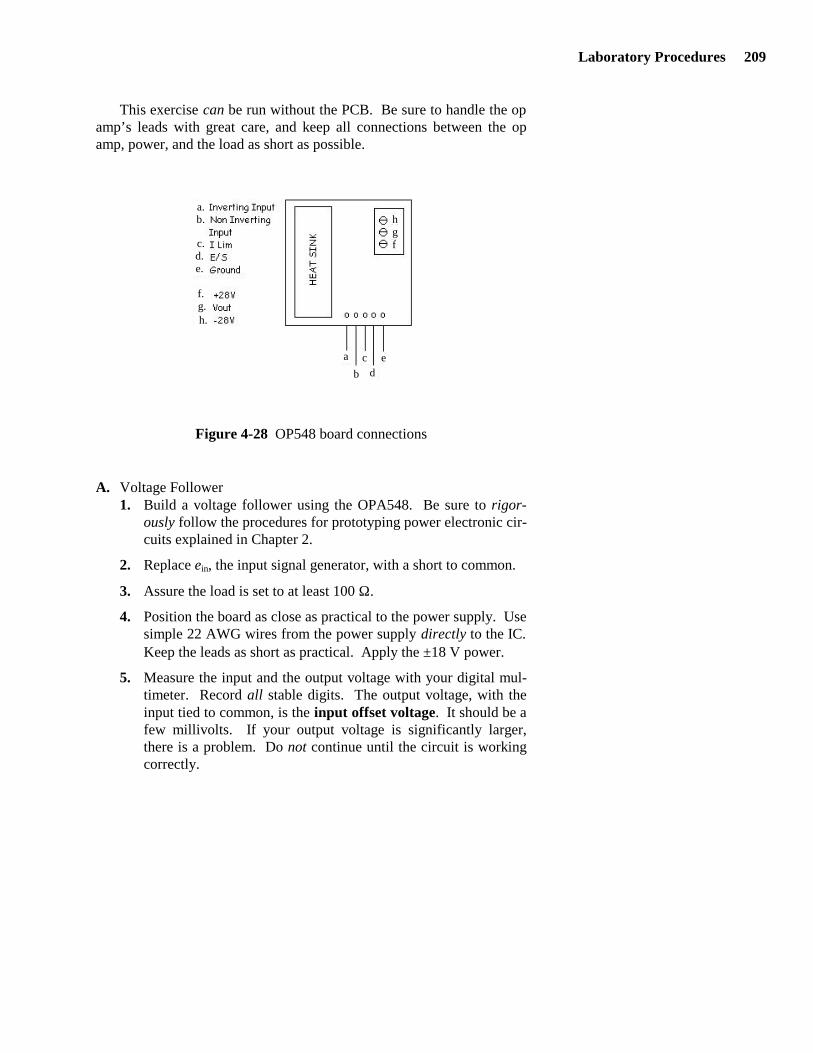
Laboratory Procedures 209
This exercise can be run without the PCB. Be sure to handle the op amp’s leads with great care, and keep all connections between the op amp, power, and the load as short as possible.
a.b.
c.d.e.
f.f.g.h.
a
bc
de
fgh
Figure 4-28 OP548 board connections
A. Voltage Follower 1. Build a voltage follower using the OPA548. Be sure to rigor-
ously follow the procedures for prototyping power electronic cir-cuits explained in Chapter 2.
2. Replace ein, the input signal generator, with a short to common.
3. Assure the load is set to at least 100 Ω .
4. Position the board as close as practical to the power supply. Use simple 22 AWG wires from the power supply directly to the IC. Keep the leads as short as practical. Apply the ±18 V power.
5. Measure the input and the output voltage with your digital mul-timeter. Record all stable digits. The output voltage, with the input tied to common, is the input offset voltage. It should be a few millivolts. If your output voltage is significantly larger, there is a problem. Do not continue until the circuit is working correctly.
Chapter 4 n Linear Power Amplifier Integrated Circuits 210
6. Replace the short to common at the input with a sine wave of 5 Vrms, 100 Hz as measured on the digital multimeter.
7. Display the input and the output on the oscilloscope.
8. When the output is an undistorted sine wave, with little offset, measure the input and the output with your digital multimeter. Record all stable digits.
9. Set the input to 0 Vrms.
10. Switch the power connections to a ±28 V, high current supply.
11. Turn the power supply on while monitoring the supply current.
12. Set the input to 5 Vrms. Gradually lower the load’s resistance un-til the supply current is 1 Adc.
13. When the output is an undistorted sine wave, with little offset, measure the input and the output with your digital multimeter. Record all stable digits.
14. Return the load to its maximum resistance and turn the power supply off.
15. Calculate the gain and compare it to theory.
B. Noninverting Amplifier
1. Build a noninverting amplifier with the OPA548. Set Rf = 33 kΩ , and Ri = 1 kΩ . Carefully review your layout to assure that it closely follows the guidelines from Chapter 2.
2. Measure the value of Rf and Ri. Record all stable digits.
3. Using these measured resistor values, calculate and record the amplifier’s theoretical gain.
4. Replace ein, the input signal, with a short to circuit common. Apply ±18 V.
5. Measure the input and the output Vdc with your digital multime-ter. Record all stable digits.
6. Compare this offset voltage with that from the voltage follower. Is it the same, or did it go up by 34? Is the input offset voltage affected by the gain?
Laboratory Procedures 211
7. Replace the short to common with a sine wave of 100 mVrms, 100 Hz as measured on the digital multimeter. Also display the input and output signals on the oscilloscope.
8. When the output is an undistorted sine wave, with little offset, measure the input and the output Vrms with your digital multime-ter. Record all stable digits.
9. Calculate the measured gain and compare it to the theoretical gain calculated (with actual resistor values) in step B3.
10. Set the input to 0 Vrms.
11. Switch the power connections to a ±28 V, high current supply.
12. Turn the power supply on while carefully monitoring the supply current.
13. Set the input to 0.5 Vrms. Gradually lower the load’s resistance to 8 Ω . The supply’s current should indicate about 1 Adc.
14. When the output is an undistorted sine wave, with little offset, measure the input and the output with your digital multimeter. Record all stable digits.
15. Calculate the gain at full load, and compare it to theory (step B3).
16. Calculate the power being delivered to the load.
C. Amplifier High Speed Performance 1. Lower the input amplitude to 20 mVrms.
2. Raise the input signal’s frequency until the gain has fallen to 0.707 of that measured in step B15. Be sure that the input am-plitude remains constant.
3.
4. This frequency is the high frequency cut-off, fH. Calculate the amplifier’s gain bandwidth product.
5. Change the input to a square wave with a 600 mVp amplitude and a 5 kHz frequency.
6. Measure the slope of the output. This slope is expressed in V/µs. This is the amplifier’s slew rate.
frequencylowH AfGBW ×=

Chapter 4 n Linear Power Amplifier Integrated Circuits 212
7. Using your amplifier’s slew rate, calculate the highest frequency a 24 Vp sine wave output can obtain before distortion begins.
8. Change the input to a sine wave and adjust its amplitude to 0.5 Vrms, at 100 Hz.
9. Raise the frequency slowly until the output begins to distort, changing into a triangle. Record that frequency and compare it to that calculated in step C7.
D. Audio Amplifier 1. Set the input signal generator to 0. Turn the power supplies off.
2. Replace the 8 Ω resistive load with a loudspeaker capable of dis-sipating at least 50 W.
3. Turn the power supplies on.
4. Gradually increase the input amplitude until the output is a clean 100 Hz, 2.83 Vrms sine wave. This signal is delivering 1 W to the loudspeaker.
5. Measure the volume in dBspl at 1 m directly in front of the loud-speaker.
6. Increase the input amplitude until the volume is slightly uncom-fortably loud.
7. Measure the rms voltage delivered to the loudspeaker. Calculate the power being delivered to the loudspeaker.
8. Measure the volume in dBspl 1 m in front of the loudspeaker. Compare the expected increase in volume with that which you just measured.
9. Move to a point 4 m directly in front of the loudspeaker. Meas-ure the volume. Did the dBspl decrease according to theory?
10. Repeat steps 4 through 8 at 1 kHz and 5 kHz. Discuss the effect of the signal’s frequency (tone).
11. Reduce the input signal’s input to 0. Replace it with a music source, with the volume all the way down.
12. Gradually increase the music source’s volume until the sound is slightly uncomfortable. Repeat steps 7 and 8. Discuss the dif-ferences in the power and sound from a sine wave and from a music source.
outpmaxsignallarge 2 V
rateslewf
π=


![04 Operational Amplifier Circuits [OAC]](https://static.fdocuments.net/doc/165x107/563db9ef550346aa9aa13cdb/04-operational-amplifier-circuits-oac.jpg)