3D IC Overview - NASA · PDF fileTezzaron Semiconductor 06/12/2012 TSV Pitch ≠ Area...
33
Transcript of 3D IC Overview - NASA · PDF fileTezzaron Semiconductor 06/12/2012 TSV Pitch ≠ Area...
Tezzaron Semiconductor 06/12/2012
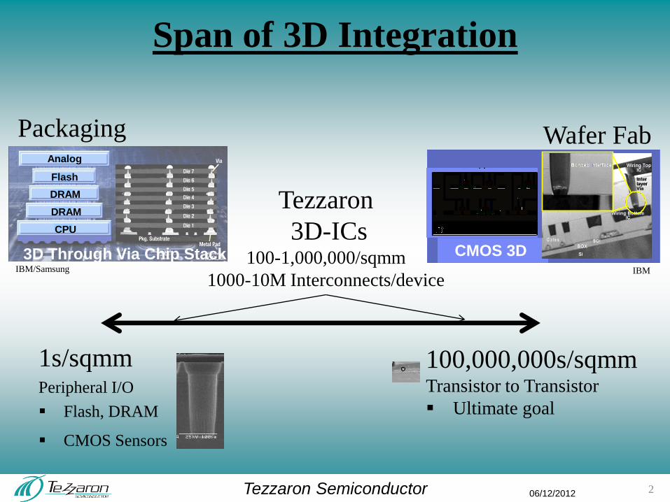
Span of 3D Integration
CMOS 3D CMOS 3D
Analog
Flash
DRAM
DRAM
CPU
Analog
Flash
DRAM
DRAM
CPU
3D Through Via Chip Stack
100,000,000s/sqmm Transistor to Transistor
Ultimate goal
1s/sqmm Peripheral I/O
Flash, DRAM
CMOS Sensors
Tezzaron
3D-ICs 100-1,000,000/sqmm
1000-10M Interconnects/device
Packaging Wafer Fab
IBM IBM/Samsung
2

Tezzaron Semiconductor 06/12/2012
10um TSV
20um Pitch
TSV Pitch ≠ Area ÷ Number of TSVs
• TSV pitch issue example – 1024 bit busses require a lot of space with larger TSVs
– They connect to the heart and most dense area of processing elements
– The 45nm bus pitch is ~100nm; TSV pitch is >100x greater
– The big TSV pitch means TOF errors and at least 3 repeater stages
F
P
U
1024 bit bus
Single layer
interconnect
3
Tezzaron Semiconductor 06/12/2012
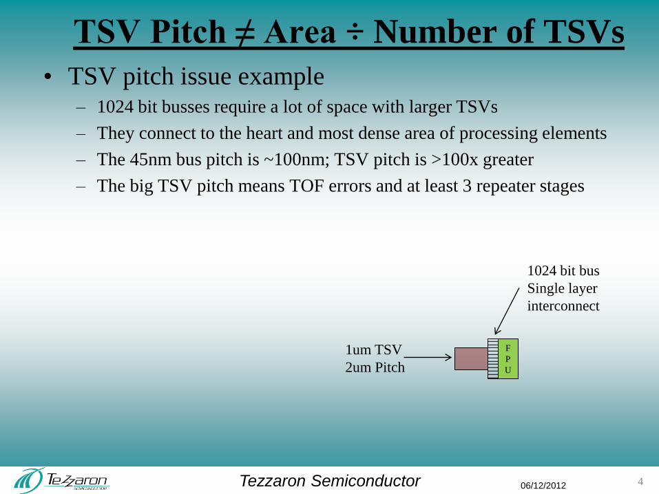
TSV Pitch ≠ Area ÷ Number of TSVs
• TSV pitch issue example – 1024 bit busses require a lot of space with larger TSVs
– They connect to the heart and most dense area of processing elements
– The 45nm bus pitch is ~100nm; TSV pitch is >100x greater
– The big TSV pitch means TOF errors and at least 3 repeater stages
F
P
U
1024 bit bus
Single layer
interconnect
1um TSV
2um Pitch
4

Tezzaron Semiconductor 06/12/2012
3D Interconnect Characteristics
SuperContactTM
I
200mm
Via First, FEOL
SuperContactTM
III
200mm
Via First, FEOL
SuperContactTM
IV
200mm
Via First, FEOL
Interposer
TSV
Bond Points Die to
Wafer
Size
L X W X D
Material
1.2 X 1.2
X 6.0
W in Bulk
0.85 X 0.85
X 10
W in Bulk
0.60 X 0.60
X 2
W in SOI
10 X 10
X 100
Cu
1.7 X 1.7
Cu
3 X 3
Cu
Minimum
Pitch
<2.5 1.75 1.2 30/120 2.4 5
Feedthrough
Capacitance
2-3fF 3fF 0.2fF 250fF << <25fF
Series
Resistance
<1.5 W <3 W <1.75 W <0.5 W < <
5
Small fine grain TSVs are fundamental to 3D enablement
Tezzaron Semiconductor 06/12/2012
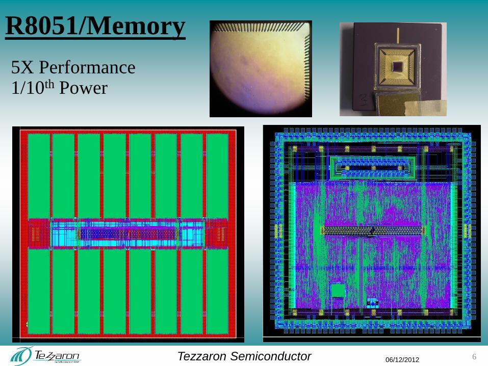
R8051/Memory
5X Performance 1/10th Power
6

Tezzaron Semiconductor 06/12/2012 7

Tezzaron Semiconductor 06/12/2012
A Closer Look at Wafer-Level Stacking
Dielectric(SiO2/SiN)
Gate Poly
STI (Shallow Trench Isolation)
Oxide
Silicon
W (Tungsten contact & via)
Al (M1 – M5)
Cu (M6, Top Metal)
“Super-Contact”
8

Tezzaron Semiconductor 06/12/2012
Next, Stack a Second Wafer & Thin:
9

Tezzaron Semiconductor 06/12/2012
Two wafer Align & Bond Course Grinded Fine Grinded
After CMP Si Recessed
Stacking Process Sequential Picture
Misalign=0.3um
Top wafer
Bottom wafer
High Precision Alignment
10

Tezzaron Semiconductor 06/12/2012
3rd wafer 2nd wafer 1st wafer: controller
Then, Stack a Third Wafer:
11

Tezzaron Semiconductor 06/12/2012
1st wafer: controller 2nd wafer 3rd wafer
Finally, Flip, Thin & Pad Out:
This is the
completed stack!
12

Tezzaron Semiconductor 06/12/2012
3rd Si thinned to 5.5um
2nd Si thinned to 5.5um
1st Si bottom supporting wafer
SiO2
13

Tezzaron Semiconductor 06/12/2012 14
TSVs

Tezzaron Semiconductor 06/12/2012
0.6um SOI TSV
15
120K TSVs

Tezzaron Semiconductor 06/12/2012
DRAM wants 2 different processes!
Bit cells Low leakage
-slow refresh
-low power
-low GIDL
High Vt Devices
Vneg Well
Thick Oxide
Sense Amps
Word line drivers
Device I/O
High speed
-better sensitivity
-better bandwidth
-lower voltage
Low Vt Devices
Copper interconnect
Thin Oxides

Tezzaron Semiconductor 06/12/2012
“Dis-Integrated” 3D Memory
Wordline Drivers
Senseamps
Memory
Cells
I/O Drivers
Memory Layers
from DRAM fab
Controller Layer
from high speed
logic fab
Bitlines Wordlines
Power,Ground,
VBB,VDH
17
2 million vertical
connections per
lay per die Better yielding than 2D equivalent!

Tezzaron Semiconductor 06/12/2012
Octopus Stack
18
DRAM Control/Logic DRAM Memory Cells
2 Layer Stacked Device
(SEM)

Tezzaron Semiconductor 06/12/2012
3D DRAMs Octopus I • 1-4Gb
• 16 Ports x 128bits (each way)
• @1GHz – CWL=0 CRL=2 SDR format
– 5ns closed page access to first data (aligned)
– 12ns full cycle memory time
– 288GB/s data transfer rate
• Max clk=1.6GHz
• Internally ECC protected, Dynamic self-repair, Post attach repair
• 115C die full function operating temperature
• JTAG/Mailbox test&configuration
Octopus II • 4-64Gb
• 64-256 Ports x 64bits (each way)
• @1GHz – 5-7ns closed page access to first data (aligned)
– 12ns full cycle memory time
– 2TB/s data transfer rate
19

Tezzaron Semiconductor 06/12/2012
The Industry Issue
1
10
100
1000
10000
Best Case Number of channels to support Float OPS
Worst Case Number of channels to support Float OPS
Best Case Number of channels to support OPS
Worst Case Number of channels to support OPS
Best Case Number of channels to support mixed OPS
DD
R2
/3/4
Mem
ory
Ch
ann
els
To continue to increase CPU
performance, exponential
bandwidth growth required.
More than 200 CPU cycles of
delay to memory results in cycle
for cycle CPU stalls.
16 to 64 Mbytes per thread
required to hide CPU memory
system accesses.
No current extension of existing
IC technology can address
requirements.
Memory I/O power is running
away.
Need 50x bandwidth improvement.
Need 10x better cost model than embedded
memory.
20

Tezzaron Semiconductor 06/12/2012
Logic on Memory
172 pads
8 DRAM ports
16x21 pad array
>10f bypass caps
SS ~4,000pf 21
Memory
Logic

Tezzaron Semiconductor 06/12/2012
Logic on Memory
172 pads 92 pads
(528 total pads at edge, stagger
250um pad, 125um pitch
~1500 available pads)
199 I/O
Bondpoints/side
>10f bypass caps
SS ~4,000pf 22
Memory also
acts as
interposer

Tezzaron Semiconductor 06/12/2012 23
David Fick of the University of
Michigan showed Centip3De, a
3-D IC stack using
128 ARM Cortex M3 cores and
256 Mbytes of stacked DRAM
operating at near threshold
voltage. (Paper 10.7)
University Michigan, ISSCC and The Register

Tezzaron Semiconductor 06/12/2012 24
Dean Lewis, another GIT researcher,
showed 3-D MAPS, a massively parallel
processor using 64 custom cores stacked
with a block 256 kilobytes of scratch pad
memory. (Paper 10.6)
Georgia Institute of Technology, ISSCC and The
Register

Tezzaron Semiconductor 06/12/2012
Tezzaron 3D
Devices June/July
2011
25

Tezzaron Semiconductor 06/12/2012
2.5/3D Circuits
26
CC
FPGA (4Xnm)
Active Silicon Circuit Board
2 Layer Processor2 Layer Processor3 Layer 3D Memory
CC
Organic Substrate
level#0
level#1
level#2
level#3
Solder Bumps
μBumps
C4 Bumps
Die to Wafer Cu Thermal Diffusion Bond
level#4
IME A-Star / Tezzaron Collaboration
IME A-Star /
Tezzaron
Collaboration

Tezzaron Semiconductor 06/12/2012
0.4 GT/s
SSTL type of eye designed
with 50 Ohm “landscape”
(75 mm long) has increased
SI penalty with Mem speed
improvement
LVCMOS type of eye on BEOL wire (e.g w/s=10/10um) with 25 mm length,TSI “landscape” are
more SI robust to Mem. speed improvement…..showing margin for design in the eye
a)For system on PCB ( each die is packaged),SSTL type of circuit are used (50 Ohm landscape design on PCB)
b) For system on TSI LVCMOS driver are used (BEOL wire design)
System in PCB vs in TSI (Courtesy A*STAR Institute of Microelectronics)
1.6GT/s
0.8GT/s
Note : R,L,C for PKG is 0.3Ω,3.7nH,2.2pF

Tezzaron Semiconductor 06/12/2012
1.6GT/s with w/s=4/2 um L=5mm
1.6GT/s with w/s=4/2 um L=25mm
1.6GT/s with w/s=10/10 um L=25mm
Layout considerations (Courtesy A*STAR Institute of Microelectronics)
•RC penalty type is reduced on long line by
using large wires(R drop) and large spacing (C
drop)
• Byte lanes [8 wires of DQ and 1 wire of DQS
(strobe)] with spacing S between wires
S=4*(W+S) to eliminate crosstalk from parallel
wires (2nd effect order)

Tezzaron Semiconductor 06/12/2012
Near End-of-Line
poly
STI
SIN M1
M2
M3
M4
M5
M6
M7
5.6µ TSV is 1.2µ
Wide and ~10µ deep
W
M8
TM
M4
M5
2x,4x,8x Wiring level
~.2/.2um S/W
29

Tezzaron Semiconductor 06/12/2012
3D EDA Tool Support
30
# 3D LVS Tech file WAFER: 1
LAYOUT TOP BLOCK: lvslayer1_1
SCHEMATIC TOP BLOCK: lvslayer1
GDSII FILE: lvslayer1_1.gds
SCHEMATIC NETLIST: lvslayer1.sp
INTERFACE UP METAL: 1;0
INTERFACE UP TEXT: 1;101
...
INTERFACE:
LAYOUT TOP BLOCK: lvstop
SCHEMATIC TOP BLOCK: lvstop
GDSII FILE: lvstop_ALL.gds
SCHEMATIC NETLIST: lvstop.sp
BOND OUT METAL: 5;0
BOND OUT TEXT: 5;101

Tezzaron Semiconductor 06/12/2012
3D Opportunities • Complete 3D PDK 8th Release
– GF 130nm
– Calibre, Synopsys, Hspice, Cadence MicroMagic 3D physical editor
– Magma 3D DRC/LVS
– Artisan standard cell libraries
• MOSIS, CMP, and CMC MPW support
– 130nm, coming soon 65nm
– Silicon Workbench
• Honeywell 150nm SOI
• 90nm NEOL TSV
• 40nm 3D logic
• IME silicon interposers, photonics
• eSilicon 3D solutions, organic interposers
• >100 devices in process
• >400 users
31

Tezzaron Semiconductor 06/12/2012
New Apps – New Architectures
32

Tezzaron Semiconductor 06/12/2012
Summary
• 3D Integration offers vast new opportunities!
– New design approaches
– New ways of thinking
– Best of class integration of
• Memory
• Logic
• RF
• MEMS
33
Sensors
Computing
MEMS
Communications