3-Wire RTD Measurement System Reference … RTD Measurement System Reference Design, -200°C to...
39
An IMPORTANT NOTICE at the end of this TI reference design addresses authorized use, intellectual property matters and other important disclaimers and information. TINA-TI is a trademark of Texas Instruments WEBENCH is a registered trademark of Texas Instruments SLAU520A-December 2013-Revised November 2014 3-Wire RTD Measurement System Reference Design, -200°C to 850°C 1 Copyright © 2013, Texas Instruments Incorporated Ryan Andrews, Collin Wells TI Designs – Precision: Verified Design 3-Wire RTD Measurement System Reference Design, -200°C to 850°C TI Designs – Precision Circuit Description TI Designs – Precision are analog solutions created by TI’s analog experts. Verified Designs offer the theory, component selection, simulation, complete PCB schematic & layout, bill of materials, and measured performance of useful circuits. Circuit modifications that help to meet alternate design goals are also discussed. This ratiometric temperature acquisition system accurately measures temperature over a wide range of -200°C to 850°C. The design uses a resistance temperature detector (RTD) in a 3-wire configuration to minimize the errors introduced by the lead resistances of a remotely located RTD. A 24-bit delta- sigma (ΔΣ) analog-to-digital converter (ADC) is used in this design which features two integrated precision current sources that excite the 3-wire RTD. The differential voltage that develops across the RTD is converted into a digital output code and translated into a final temperature result. Design Resources Design Archive All Design files TINA-TI™ SPICE Simulator ADS1247 Product Folder TPS7A4901 Product Folder Ask The Analog Experts WEBENCH® Design Center TI Designs – Precision Library REFP REFN MUX AIN0/IEXC1 AIN1 AIN2 AIN3/IEXC2 IDAC Excitation Current Sources PGA ΔΣ ADC Reference Buffer/MUX RREF RRTD ADS1247 RI1 RI2 CI_CM1 CI_DIFF CI_CM2 CR_CM1 CR_CM2 CR_DIFF RR1 RR2
Transcript of 3-Wire RTD Measurement System Reference … RTD Measurement System Reference Design, -200°C to...

An IMPORTANT NOTICE at the end of this TI reference design addresses authorized use, intellectual property matters and other important disclaimers and information.
TINA-TI is a trademark of Texas Instruments WEBENCH is a registered trademark of Texas Instruments
SLAU520A-December 2013-Revised November 2014 3-Wire RTD Measurement System Reference Design, -200°C to 850°C 1 Copyright © 2013, Texas Instruments Incorporated
Ryan Andrews, Collin Wells
TI Designs – Precision: Verified Design
3-Wire RTD Measurement System Reference Design, -200°C to 850°C
TI Designs – Precision Circuit Description
TI Designs – Precision are analog solutions created by TI’s analog experts. Verified Designs offer the theory, component selection, simulation, complete PCB schematic & layout, bill of materials, and measured performance of useful circuits. Circuit modifications that help to meet alternate design goals are also discussed.
This ratiometric temperature acquisition system accurately measures temperature over a wide range of -200°C to 850°C. The design uses a resistance temperature detector (RTD) in a 3-wire configuration to minimize the errors introduced by the lead resistances of a remotely located RTD. A 24-bit delta-sigma (ΔΣ) analog-to-digital converter (ADC) is used in this design which features two integrated precision current sources that excite the 3-wire RTD. The differential voltage that develops across the RTD is converted into a digital output code and translated into a final temperature result.
Design Resources
Design Archive All Design files TINA-TI™ SPICE Simulator ADS1247 Product Folder TPS7A4901 Product Folder
Ask The Analog Experts WEBENCH® Design Center TI Designs – Precision Library
REFP REFN
MUX
AIN0/IEXC1
AIN1
AIN2
AIN3/IEXC2
IDACExcitationCurrentSources
PGAΔΣ
ADC
Reference
Buffer/MUX
RREF
RRTD
ADS1247
RI1
RI2
CI_CM1
CI_DIFF
CI_CM2
CR_CM1 CR_CM2CR_DIFF
RR1 RR2
www.ti.com
2 3-Wire RTD Measurement System Reference Design, -200°C to 850°C SLAU520A-December 2013-Revised November 2014 Copyright © 2013, Texas Instruments Incorporated
1 Design Summary
The design requirements are as follows:
RTD Type: 3-Wire Pt100
Temperature Measurement Range: -200°C to 850°C
Temperature Measurement Accuracy: ±0.05°C at TA = 25°C
System Supply Voltage (VDUT): 5 V
ADC Supply Voltage (AVDD): 3.3 V
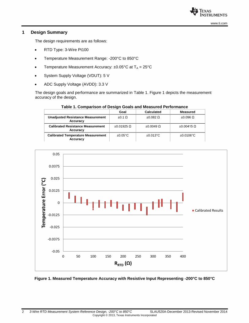
The design goals and performance are summarized in Table 1. Figure 1 depicts the measurement accuracy of the design.
Table 1. Comparison of Design Goals and Measured Performance
Figure 1. Measured Temperature Accuracy with Resistive Input Representing -200°C to 850°C
-0.05
-0.0375
-0.025
-0.0125
0
0.0125
0.025
0.0375
0.05
0 50 100 150 200 250 300 350 400
Tem
pe
ratu
re E
rro
r (°
C)
RRTD (Ω)
Calibrated Results
Goal Calculated Measured
Unadjusted Resistance Measurement Accuracy
±0.1 Ω ±0.082 Ω ±0.096 Ω
Calibrated Resistance Measurement Accuracy
±0.01925 Ω ±0.0049 Ω ±0.00415 Ω
Calibrated Temperature Measurement Accuracy
±0.05°C ±0.013°C ±0.0106°C
www.ti.com
SLAU520A-December 2013-Revised November 2014 3-Wire RTD Measurement System Reference Design, -200°C to 850°C 3 Copyright © 2013, Texas Instruments Incorporated
2 Theory of Operation
2.1 Resistance Temperature Detector (RTD) Overview
An RTD is a sensing element made of a metal with predictable resistance characteristics over temperature. The temperature of an RTD can therefore be calculated by measuring the resistance. RTD sensors offer wide temperature ranges, good linearity, and excellent long-term stability and repeatability, making them suitable for many precision measurement applications.
The relationship between resistance and temperature of an RTD is defined by the Callendar-Van Dusen (CVD) equations which can be found in Appendix A.4.
Compared to a thermocouple, the main disadvantages of RTD sensors are their cost and required excitation source. The small change in resistance of an RTD over temperature also places demands on the accuracy of the acquisition circuit requiring a precision signal chain. Thermistors have larger changes in resistance over temperature but are much less linear, reducing their effectiveness at measuring wider temperature ranges.
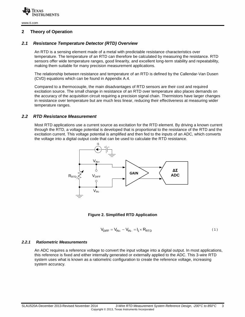
2.2 RTD Resistance Measurement
Most RTD applications use a current source as excitation for the RTD element. By driving a known current through the RTD, a voltage potential is developed that is proportional to the resistance of the RTD and the excitation current. This voltage potential is amplified and then fed to the inputs of an ADC, which converts the voltage into a digital output code that can be used to calculate the RTD resistance.
RRTD
VIN-
VIN+
VDIFF
ΔΣ
ADCGAIN
I1
Figure 2. Simplified RTD Application
RTD1ININDIFF RIVVV ( 1 )
2.2.1 Ratiometric Measurements
An ADC requires a reference voltage to convert the input voltage into a digital output. In most applications, this reference is fixed and either internally generated or externally applied to the ADC. This 3-wire RTD system uses what is known as a ratiometric configuration to create the reference voltage, increasing system accuracy.

www.ti.com
4 3-Wire RTD Measurement System Reference Design, -200°C to 850°C SLAU520A-December 2013-Revised November 2014 Copyright © 2013, Texas Instruments Incorporated
In the ratiometric configuration shown in Figure 3, the excitation current that flows through the RTD returns to ground through a low-side reference resistor, RREF. The voltage potential developed across RREF, VREF, is fed into the positive and negative reference pins (REFP and REFN) of the ADC. VREF serves three purposes in this design: it sets the input common-mode voltage (VCM), the differential ADC input range (typically ±VREF), and it is also used to convert the input voltage into digital output codes. See Equations ( 2 ) – ( 6 ).
Setting VREF to mid-supply results in optimal input circuit performance for the ADC. RREF should be selected with low tolerance and low drift since errors in the reference voltage will directly translate into errors in the conversion result.
GAINΔΣ
ADC
RREF
RRTD
REFP REFN
I1
VIN-
VIN+
VDIFF
Figure 3. Ratiometric RTD Measurement
REF1CMREF RIVV ( 2 )
Gain
VV
Gain
V REFDIFF
REF
( 3 )
The voltage drop across the RTD and RREF resistors is produced by the same excitation source in a ratiometric configuration as shown in Equations ( 4 ) - ( 5 ). Therefore, any changes in the excitation source are reflected in both the RTD differential voltage and the reference voltage. Since the ADC output code is a relationship between the input voltage and the reference voltage, the final conversion result is simply a ratio of the RTD and RREF resistances as shown in Equation ( 6 ). Consequently, inaccuracies due to magnitude, temperature drift, and noise of the current source cancel without affecting the final conversion result. The ratiometric configuration also helps reduce the effects of external noise that appears common to both the inputs and the reference because it should cancel as well.
RTD1RTDDIFF RIVV ( 4 )
REF1REF RIV ( 5 )

www.ti.com
SLAU520A-December 2013-Revised November 2014 3-Wire RTD Measurement System Reference Design, -200°C to 850°C 5 Copyright © 2013, Texas Instruments Incorporated
REF
RTDTOTAL
REF
DIFFTOTALIDEAL
R2
GainRCodes
V2
GainVCodesCode ( 6 )
2.2.2 Current Sources
Two precision current sources are typically used in 3-wire RTD applications to provide an easy way to cancel the RTD lead resistances (RLEAD) as shown in Figure 4. This technique works best when the two current sources are well-matched, both in initial accuracy and temperature drift. For additional information on other RTD configurations, refer to Reference 2.
Equations ( 7 ) – ( 10 ) derive the final differential input voltage and prove that RLEAD is excluded from the final result.
Figure 4. 3-Wire RTD Lead Resistances Canceled by Excitation Currents
III 21 ( 7 )
RTDREFLEADIN
REFLEADRTDLEADIN
RI + RI2 +RI3 =V
)R+(RI2+)R(RI = V
( 8 )
REFLEAD-IN
REFLEADLEAD-IN
RI2 + RI3 =V
)R+(RI2RI = V
( 9 )
RTD-ININ DIFF RI =V- V=V ( 10 )
With two current sources flowing through RREF in this 3-wire RTD system, the VREF voltage doubles as shown in Equation ( 11 ). Therefore, the final conversion result transfer function also changes as shown in Equation ( 12 ).
RREF
RLEAD
RLEAD
RLEAD
I1
GAINΔΣ
ADC
REFP REFN
I2
VIN-
VIN+
VDIFF
I1
I2
I1 + I2
RRTD
www.ti.com
6 3-Wire RTD Measurement System Reference Design, -200°C to 850°C SLAU520A-December 2013-Revised November 2014 Copyright © 2013, Texas Instruments Incorporated
REFREF RI2V ( 11 )
REF
RTDTOTALOUTPUT
R4
GainRCodesCode ( 12 )
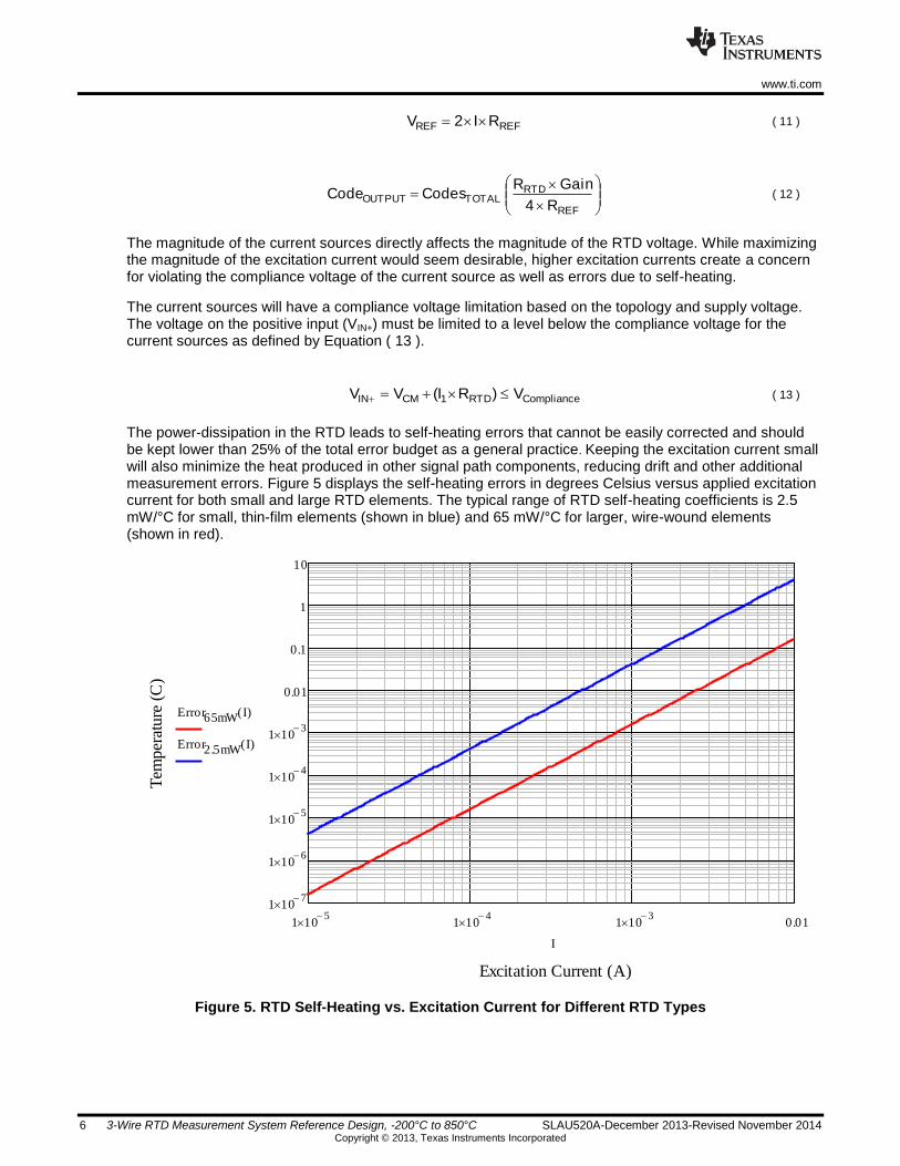
The magnitude of the current sources directly affects the magnitude of the RTD voltage. While maximizing the magnitude of the excitation current would seem desirable, higher excitation currents create a concern for violating the compliance voltage of the current source as well as errors due to self-heating.
The current sources will have a compliance voltage limitation based on the topology and supply voltage. The voltage on the positive input (VIN+) must be limited to a level below the compliance voltage for the current sources as defined by Equation ( 13 ).
ComplianceRTD1CMIN V)RI(VV ( 13 )
The power-dissipation in the RTD leads to self-heating errors that cannot be easily corrected and should be kept lower than 25% of the total error budget as a general practice. Keeping the excitation current small will also minimize the heat produced in other signal path components, reducing drift and other additional measurement errors. Figure 5 displays the self-heating errors in degrees Celsius versus applied excitation current for both small and large RTD elements. The typical range of RTD self-heating coefficients is 2.5 mW/°C for small, thin-film elements (shown in blue) and 65 mW/°C for larger, wire-wound elements (shown in red).
Figure 5. RTD Self-Heating vs. Excitation Current for Different RTD Types
1 105
1 104
1 103
0.01
1 107
1 106
1 105
1 104
1 103
0.01
0.1
1
10
Self-Heating Error of an RTD vs. Excitation Current
Excitation Current (A)
Tem
per
ature
(C
)
Error65mW I( )
Error2.5mW I( )
I

www.ti.com
SLAU520A-December 2013-Revised November 2014 3-Wire RTD Measurement System Reference Design, -200°C to 850°C 7 Copyright © 2013, Texas Instruments Incorporated
The effects of self-heating on measurement accuracy are also based on the placement of the RTD in the application. The effects of self-heating are reduced if the RTD is placed in a moving fluid medium because the moving fluid will keep the RTD close to the temperature of the fluid. However, in open-air temperature measurements, or other applications where the RTD is surrounded by an insulator, the RTD will self-heat and cause errors.
2.2.3 Amplification Stage
The full-scale input range of an ADC is bounded by the reference voltage, VREF. By choosing a smaller value for the excitation current to reduce self-heating, the RTD produces a smaller change in voltage over the span of the temperature measurement that will not use the full ADC input range. Therefore, a gain stage is required to amplify the RTD voltage to a level that utilizes more of the range of the full-scale ADC input, VIN_ADC, and maximizes the measurement resolution.
GainRIV RTD1ADC_IN ( 14 )
The gain must be selected such that neither the full-scale input voltage nor the common-mode input voltage is violated. Both limitations are typically found in the device specifications section of the data converter datasheet.
2.2.4 Input and Reference Low-Pass Filters
Using differential and common-mode low-pass filters at the input and reference paths improves the cancellation of excitation and environmental noise. However, it is important to note that the corner frequency of the two differential filters must be well-matched as stated in Reference 1. The input and reference filters are shown in Figure 6.
Figure 6. Input and Reference Low-Pass Filtering
GAINΔΣ
ADC
RREF
RRTD
I1
I2
REFP REFN
RR1 RR2
RI1
RI2
CI_CM1
CI_DIFF
CI_CM2
CR_CM1 CR_CM2CR_DIFF
www.ti.com
8 3-Wire RTD Measurement System Reference Design, -200°C to 850°C SLAU520A-December 2013-Revised November 2014 Copyright © 2013, Texas Instruments Incorporated
3 Component Selection
3.1 ADC – ADS1247
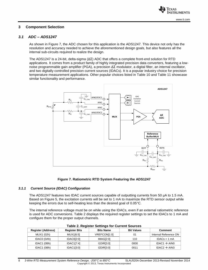
As shown in Figure 7, the ADC chosen for this application is the ADS1247. This device not only has the resolution and accuracy needed to achieve the aforementioned design goals, but also features all the internal sub-circuits required to realize the design.
The ADS1247 is a 24-bit, delta-sigma (ΔΣ) ADC that offers a complete front-end solution for RTD applications. It comes from a product family of highly integrated precision data converters, featuring a low-noise programmable gain amplifier (PGA), a precision ΔΣ modulator, a digital filter, an internal oscillator, and two digitally controlled precision current sources (IDACs). It is a popular industry choice for precision temperature measurement applications. Other popular choices listed in Table 10 and Table 11 showcase similar functionality and performance.
REFP REFN
MUX
AIN0/IEXC1
AIN1
AIN2
AIN3/IEXC2
IDACExcitationCurrentSources
PGAΔΣ
ADC
Reference
Buffer/MUX
RREF
RRTD
ADS1247
RI1
RI2
CI_CM1
CI_DIFF
CI_CM2
CR_CM1 CR_CM2CR_DIFF
RR1 RR2
Figure 7. Ratiometric RTD System Featuring the ADS1247
3.1.1 Current Source (IDAC) Configuration
The ADS1247 features two IDAC current sources capable of outputting currents from 50 µA to 1.5 mA. Based on Figure 5, the excitation currents will be set to 1 mA to maximize the RTD sensor output while keeping the errors due to self-heating less than the desired goal of 0.05°C.
The internal reference voltage must be on while using the IDACs, even if an external ratiometric reference is used for ADC conversions. Table 2 displays the required register settings to set the IDACs to 1 mA and configure them for the proper output channels.
Table 2. Register Settings for Current Sources
Register (Address) Register Bits Bits Name Bit Values Comment
MUX1 (02h) MUX1[6:5] VREFCON[1:0] 01 Internal Reference ON
IDAC0 (0Ah) IDAC0[2:0] IMAG[2:0] 110 IDACs = 1 mA
IDAC1 (0Bh) IDAC1[7:4] I1DIR[3:0] 0000 IDAC1 AIN0
IDAC1 (0Bh) IDAC1[3:0] I2DIR[3:0] 0011 IDAC2 AIN3

www.ti.com
SLAU520A-December 2013-Revised November 2014 3-Wire RTD Measurement System Reference Design, -200°C to 850°C 9 Copyright © 2013, Texas Instruments Incorporated
3.1.2 IDAC Multiplex Chopping
As the equations in Section 2.2.2 show, the two current sources must be exactly matched to successfully cancel the lead resistances of the RTD wires. While initial matching of the current sources is important, any remaining mismatch in the two sources can be minimized by using a multiplexer to swap, or “chop,” the two current sources between the two inputs. Taking measurements in both configurations and averaging the readings will greatly reduce the effects of mismatched current sources. This design uses the digitally-controlled multiplexer in the ADS1247 to realize this technique. The multiplexer also affords the user some additional flexibility when routing the input voltage signals and excitation current sources on their printed circuit board (PCB) layout.
3.1.3 Programmable Gain Amplifier (PGA) Configuration
In this application, the ADC uses a 3.3 V supply for both the analog (AVDD) and digital (DVDD) power supplies. The excitation currents and RREF have been selected to produce a 1.64 V reference, allowing for a differential input signal range of ±1.64 V into the ΔΣ modulator. The maximum allowable PGA gain setting is based on the reference voltage, the RTD resistance change, and the excitation current as shown in Equations ( 15 ) – ( 17 ).
48.390R C850@RTD ( 15 )
mV48.390V
mA148.390IRV
MAX_IN
IDACC850@RTDMAX_IN
( 16 )
V
V2.4
V39048.0
V64.1
V
VGain
MAX_IN
REFMAX ( 17 )
The PGA gain is set to the closest ADS1247 PGA gain that is below the maximum value calculated in Equation ( 17 ). The PGA will be set to 4 V/V, as shown in Table 3.
Table 3. Register Settings for PGA
Register (Address) Register Bits Bits Name Bit Values Comment
SYS0 (03h) SYS0[6:4] PGA[2:0] 010 PGA = 4 V/V
3.2 Passive Components
3.2.1 RREF
The value of RREF is selected based on the IDAC setting and the desired VREF voltage of 1.64 V, as shown in Equations ( 18 ) – ( 19 ).
IDAC
REFREF
I2
VR
( 18 )
820mA12
V64.1RREF ( 19 )

www.ti.com
10 3-Wire RTD Measurement System Reference Design, -200°C to 850°C SLAU520A-December 2013-Revised November 2014 Copyright © 2013, Texas Instruments Incorporated
An 820 Ω RREF resistor was chosen based on the results of Equation ( 19 ). Since the voltage across the RREF sets the reference voltage for the ADC, the tolerance and temperature drift of RREF directly affect the measurement gain error as shown in Section 4.2.2.1 and Appendix A.5.1. To meet the un-calibrated accuracy requirement of 0.1 Ω (or 0.027% of the full-scale resistance range), a resistor with 0.02% maximum tolerance was selected.
Note that, as with any amplifier, it is necessary to ensure that the input voltage stays within the specified common-mode input range listed in the device datasheet specification table. The common-mode input voltage (VCM) to the PGA must stay within the range shown in Equation ( 20 ) based on the maximum RTD voltage.
V42.2VmV881
2
GainVV1.0AVDDV
2
GainVV1.0AVSS
CM
MAX_INCM
MAX_IN
( 20 )
For the IDACs to remain operational, the AIN0 and AIN3 inputs of the ADS1247 must satisfy the IDAC compliance voltage found in the ADS1247 datasheet (see Equation ( 21 )). The largest voltage will be seen at AIN0 as it equals the sum of the common-mode voltage and the maximum RTD voltage shown in Equation ( 22 ).
V6.2V7.0AVDD0AIN ( 21 )
V03.2mV48.390V64.1VV0AIN MAX_INCM ( 22 )
In this ratiometric configuration, VREF sets the input common-mode voltage at 1.64 V, satisfying the requirements for both the input common-mode voltage and the IDAC compliance voltage of the ADS1247.
3.2.2 Input and Reference Low-Pass Filters
The differential filters chosen for this application were designed to have a -3 dB corner frequency at least 10 times larger than the bandwidth of the ADC. The selected ADS1247 sampling rate of 20 SPS results in a -3dB bandwidth of 14.8 Hz. The -3dB filter corner frequency was set to be roughly 250 Hz at mid-scale measurement resistance. For proper operation, the differential cutoff frequencies of the reference and input low-pass filters must be well matched. This can be difficult because as the resistance of the RTD changes over the span of the measurement, the filter cutoff frequency changes as well. To mitigate this effect, the two resistors used in the input filter (RI1 and RI2) were chosen to be two orders of magnitude larger than the RTD. Input bias currents of the ADC will cause a voltage drop across the filter resistors that will show up as a differential offset error if the bias currents and/or filter resistors are not equal. Limiting the resistors to at most 20 kΩ will reduce dc offset errors due to input bias current.
k09.9RR 2I1I ( 23 )
The input filter differential capacitor (CI_DIFF) can be calculated as shown in Equation ( 24 ).
www.ti.com
SLAU520A-December 2013-Revised November 2014 3-Wire RTD Measurement System Reference Design, -200°C to 850°C 11 Copyright © 2013, Texas Instruments Incorporated
nF33C
)RRR(C2
1f
DIFF_I
2IRTD1IDIFF_IDIFF_dB3
( 24 )
To ensure that mismatch of the common-mode filtering capacitors is not translated to a differential voltage, the common-mode capacitors (CI_CM1 and CI_CM2) were chosen to be ten times smaller than the differential capacitor, making them 3.3 nF each. This results in a common-mode cutoff frequency that is roughly twenty times larger than the differential filter, making the matching of the common-mode cutoff frequencies less critical.
nF3.3CC 2CM_I1CM_I ( 25 )
kHz4.76 = f
)RRR(C2
1f
CM_dB3
REFRTD1I1CM_ICM_dB3
( 26 )
kHz4.87 =f
)RR(C2
1f
CM_dB3
REF2I2CM_INCM_dB3
( 27 )
The differential reference filter is designed to have a -3 dB corner frequency of 250 Hz to match the differential input filter. The two reference filter resistors were selected to be 20 kΩ, several times larger than the value of RREF. The reference filter resistors should not be sized larger than 20 kΩ or dc bias errors will become significant.
k20RR 2R1R ( 28 )
The differential capacitor for the reference filter can be calculated as shown in Equation ( 29 ).
nF15C
)RRR(C2
1f
DIFF_R
2RREF1RDIFF_RDIFF_dB3
( 29 )
To ensure that mismatch of the common-mode filtering capacitors is not translated to a differential voltage, the reference common-mode capacitors (CR_CM1 and CR_CM2) were chosen to be ten times smaller than the reference differential capacitor, making them 1.5 nF each. Again, the resulting cutoff frequency for the common-mode filters is roughly twenty times larger than the differential filter, making the matching of the cutoff frequencies less critical.
nF5.1CC 2CM_R1CM_R ( 30 )

www.ti.com
12 3-Wire RTD Measurement System Reference Design, -200°C to 850°C SLAU520A-December 2013-Revised November 2014 Copyright © 2013, Texas Instruments Incorporated
kHz10.5f
)RR(C2
1f
dB3
REF1R1CM_RCM_dB3
( 31 )
kHz31.5f
RC2
1f
dB3
2R2CM_RCM_dB3
( 32 )
3.3 Low-Dropout (LDO) Linear Regulator
The RTD acquisition board in this design interfaces with an external PC GUI through a USB interface board to post-process the ADC digital output and display the temperature result. Power for the acquisition board comes from the USB power supply rail (VDUT). This supply may be passed through a high-PSRR low-dropout regulator (LDO) to create the AVDD and DVDD supplies and to avoid inaccuracies due to power supply noise.
The TPS7A4901 comes from a series of high-voltage, ultra-low noise LDOs that are ideal for precision applications. A resistor divider at the LDO output sets the output voltage (VLDO_OUT) proportional to the LDO’s internal reference voltage (VLDO_REF). For this device, VLDO_REF = 1.188 V. In order to set VLDO_OUT to the desired output voltage of 3.3 V, the resistor divider components are selected using Equation ( 33 ).
k7.782R
k1401R
2R
1R1VV REF_LDOOUT_LDO
( 33 )
VOUT
0.01µF
0.1µF 10µF
140k
78.7k
0.1µF10µF
0.01µF
VDUT
TPS7A4901
OUT
FB
GND
IN
EN
NR/SS
Figure 8. LDO Configuration for +3.3 V Output

www.ti.com
SLAU520A-December 2013-Revised November 2014 3-Wire RTD Measurement System Reference Design, -200°C to 850°C 13 Copyright © 2013, Texas Instruments Incorporated
4 Simulation and Error Calculation
4.1 Simulation
Figure 9 shows the TINA-TI™ circuit used to simulate the behavior of the RTD, input filtering, and PGA in this system. The RTD has been modeled with a Pt100 macromodel that converts an input voltage representative of the RTD temperature into the correct output resistance using the CVD equations. The simplified ADS1247 PGA does not accurately represent the internal circuitry to the ADC; however, it does represent the ideal behavior of the internal PGA.
Figure 9. TINA-TITM
Simulation Circuit for the RTD and ADS1247 Inputs
VREF_INT
VREF_INT
VREF
VREFN
VREFP
AINP
AINN
VREF
IDAC1
IDAC2
IDAC2 1m
RI2 9.09k
RI1 9.09k
CIN_DIFF 33n
CI_CM1 3.3n
CI_CM2 3.3n
-
+
VIN_PGA
R7 1k
R8 4
k
R9 1k
R10 4k
-
+
IOP3
-
+
IOP4
-
+
IOP1
RREF 820
RR2 20k
RR1 20k
CR_DIFF 15n
CR_CM1 1.5n
CR_CM2 1.5n
-
+3_VIN_ADC
IDAC1 1m
VT+
VT-
Mon+ Mon-
RTD+
RTD-
U1 RTD3
TEMP 100
V+
1_R_RTD
V+
2_V_RTD
VIN_ADC-
VIN_ADC+
-
+
IOP2
-
+
IOP5
-
+VREF_ADC
4_VREF
Pt100 RTD
Temp (C)
(Volts = degrees C)
RTD Resistance
(Volts = Ohms)
ADS1247 PGA

www.ti.com
14 3-Wire RTD Measurement System Reference Design, -200°C to 850°C SLAU520A-December 2013-Revised November 2014 Copyright © 2013, Texas Instruments Incorporated
4.1.1 RTD Transfer Function
Figure 10 displays the RTD resistance, RTD voltage, ADC input voltage, and the VREF voltage as the RTD temperature is swept from -200°C to 850°C. The results are displayed on the image for the minimum, mid-scale, and maximum temperatures. The RTD voltage spans from 18.51 mV to 390.48 mV and with the PGA set to 4 V/V, the differential ADC input is from 74.03 mV to 1.56 V. The VREF voltage is also displayed and is the expected value of 1.64 V.
Figure 10. RTD, ADC, and VREF from -200°C to 850°C
T
Temperature (oC)
-200 -50 100 250 400 550 700 850
RTD ( )
0
400
V_RTD (V)
0
400m
VIN_ADC (V)
0
2
VREF (V)
0
3
R_RTD A:(-200; 18.51)
V_RTD A:(-200; 18.51m)
VIN_ADC A:(-200; 74.03m)
VREF A:(-200; 1.64)
R_RTD A:(0; 100)
V_RTD A:(0; 100m)
VIN_ADC A:(0; 400m)
VREF A:(0; 1.64)
R_RTD A:(850; 390.48)
V_RTD A:(850; 390.48m)
VIN_ADC A:(850; 1.56)
VREF A:(850; 1.64)
www.ti.com
SLAU520A-December 2013-Revised November 2014 3-Wire RTD Measurement System Reference Design, -200°C to 850°C 15 Copyright © 2013, Texas Instruments Incorporated
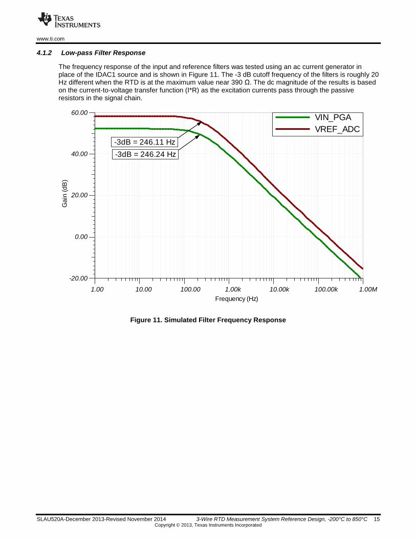
4.1.2 Low-pass Filter Response
The frequency response of the input and reference filters was tested using an ac current generator in place of the IDAC1 source and is shown in Figure 11. The -3 dB cutoff frequency of the filters is roughly 20 Hz different when the RTD is at the maximum value near 390 Ω. The dc magnitude of the results is based on the current-to-voltage transfer function (I*R) as the excitation currents pass through the passive resistors in the signal chain.
Figure 11. Simulated Filter Frequency Response
T
-3dB = 246.24 Hz
-3dB = 246.11 Hz
Frequency (Hz)
1.00 10.00 100.00 1.00k 10.00k 100.00k 1.00M
Ga
in (
dB
)
-20.00
0.00
20.00
40.00
60.00
-3dB = 246.24 Hz
VIN_PGA
VREF_ADC
-3dB = 246.11 Hz

www.ti.com
16 3-Wire RTD Measurement System Reference Design, -200°C to 850°C SLAU520A-December 2013-Revised November 2014 Copyright © 2013, Texas Instruments Incorporated
4.2 Error Calculations
4.2.1 Measurement Resolution
The smallest signal an n-bit data converter can theoretically resolve is given by its LSB size (least-significant bit). An increase in input voltage by one LSB will increment the ADC output by one code. Equation ( 34 ) calculates the weight of one LSB referred to the input of the PGA using VREF, Gain, and the number of codes.
nV88.48
2V
V4
V64.12
2Gain
V2)V(LSB
24n
REF
( 34 )
To calculate the theoretical achievable code step size in terms of resistance, divide the LSB size by the excitation current used to excite the RTD, as shown in Equation ( 35 ).
88.48mA1
nV88.48
I
)V(LSB)(LSB
IDAC
( 35 )
Since the input-referred peak-to-peak noise of the ADS1247 at 20 SPS and Gain = 4 V/V is greater than one LSB, a more appropriate resolution calculation replaces the converter LSB weight with the input-referred noise specification. The ADC datasheet will typically provide the input-referred noise (in μVPP or μVRMS) for different supply voltages, reference voltages, data rates, and gain settings.
The ADS1247 input-referred noise specification for the closest configuration to this system is 5.94 μVPP
(see Table 5 in the ADS1247 datasheet). Equation ( 36 ) calculates the ADC resistance measurement resolution based on the input-referred peak-to-peak noise (NoiseRTI_pp). The NoiseRTI_pp value is divided by factor of two to show the resolution as a deviation from the mean value.
m97.2mA1
)2/V94.5(
I
)2/Noise()(ADC
PP
IDAC
pp_RTIRES ( 36 )
The expected temperature resolution in degrees Celsius can be calculated by dividing the expected resistance resolution by the RTD sensitivity (α) as shown in Equation ( 37 ). Appendix A.4 explains how the value of α changes over the RTD measurement temperature, ranging from 0.4323 Ω/°C at -200°C to 0.2927 Ω/°C at 850°C. Therefore, the temperature resolution will vary over the RTD temperature range, even though the resistance measurement resolution will remain constant.
Equation ( 37 ) calculates the ADC resolution in degrees Celsius using the Pt100 sensitivity at 0°C.
C0076.0
C39083.0
m97.2)(ADC)C(ADC
C0@
RESC0@RES
( 37 )
4.2.2 Measurement Accuracy
The expected accuracy of the design can be calculated using the specifications of the components selected in Section 3. The units associated with these specifications range from volts, to percent full-scale range (%FSR), to parts-per-million of full-scale (ppm). In order to calculate the total error, these different errors sources must be converted to a common unit of measurement. In the following calculations, all specifications will be converted to volts referred to the input (RTI) of the ADS1247.
www.ti.com
SLAU520A-December 2013-Revised November 2014 3-Wire RTD Measurement System Reference Design, -200°C to 850°C 17 Copyright © 2013, Texas Instruments Incorporated
Gain errors will be referenced to the maximum differential input voltage, VIN_MAX = 390.48 mV (calculated in Equation ( 16 ) in Section 3.1.3), to properly calculate the input-referred voltage errors.
4.2.2.1 Errors due to RREF
The tolerance of RREF will produce gain errors in the ADC transfer function as derived in Appendix A.6.
Assuming the tolerance is specified as a percentage, the transfer function gain error from the RREF tolerance can be calculated from Equations ( 38 ) – ( 39 ).
%02.0(%)R TolREF ( 38 )
%019996.010010002.0
02.0100
100(%)R
(%)R(%)ErrorGain
TolREF
TolREF
TolRREF
( 39 )
The error in volts due to the RREF tolerance can be calculated from the gain error and the maximum input voltage.
V0804.78mV48.390100
019996.0)V(ErrorGain
V100
(%)ErrorGain)V(ErrorGain
TolR
MAX_IN
TolR
TolR
REF
REF
REF
( 40 )
4.2.2.2 Errors due to ADS1247
The ADS1247 will cause errors due to the offset voltage, offset voltage drift, gain error, gain error drift, integral nonlinearity (INL), and IDAC matching.
Offset voltage error and offset voltage error drift are commonly specified in an input-referred voltage and can be directly entered from the device performance datasheet, if provided.
V15)V(ErrorOffset ADC ( 41 )
Gain errors are usually specified as a percentage of the full-scale ADC input range (%FSR), so the input-referred voltage error can be calculated by multiplying by VIN_MAX. Equation ( 42 ) uses the typical gain error of the ADS1247, but similar errors can be calculated using the maximum specifications as well.
V524.19mV48.390100
005.0V
100
(%)ErrorGain)V(ErrorGain MAX_IN
ADCADC ( 42 )
The INL is typically specified in either number of ADC codes or in ppm FSR. Because INL is not a gain error, it must be multiplied by the full-scale input voltage of the ADC rather than VIN_MAX, as shown in Equation ( 43 ).

www.ti.com
18 3-Wire RTD Measurement System Reference Design, -200°C to 850°C SLAU520A-December 2013-Revised November 2014 Copyright © 2013, Texas Instruments Incorporated
V92.4
V
V4
V64.12
000,000,1
ppm6
Gain
V2
000,000,1
INL)V(ErrorINL REF
ADC
( 43 )
The final errors considered for this system are caused by the mismatching of the IDAC current sources which introduce a gain error in the transfer function as derived in Appendix A.7.
%07494.010020015.0
15.0100
200(%)I
(%)I(%)ErrorGain
MismatchIDAC
MismatchIDAC
IDAC
( 44 )
V626.292mV48.390100
07494.0V
100
(%)ErrorGain)V(ErrorGain MAX_IN
IDACIDAC ( 45 )
The errors from the mismatch of the IDAC sources are the largest errors in the system. This reinforces the importance of chopping the two IDAC current sources to remove these errors as described in Section 3.1.2.
4.2.2.3 Total Error
With all of the input-referred errors calculated in volts, the total error can be calculated by taking the root-sum-of-square of all of the uncorrelated error terms. A similar calculation can be performed for the maximum error by replacing the typical specifications with the maximum specifications. For cases where a typical specification is not available, the maximum specification is used.
V903.303)V(Error
ErrorGainErrorINL
ErrorGainErrorOffsetErrorGain)V(Error
Total
2IDAC
2ADC
2ADC
2ADC
2TolR
TotalREF
( 46 )
The system errors and their resulting input-referred error in μV are summarized in Table 4.
Table 4. Summary of Error Sources and Resulting Voltage Error RTI
After removing the IDAC mismatch errors with chopping, a two-point gain and offset calibration can remove the errors from the RREF tolerance, offset voltage, and gain error, leaving only the error from INL. Table 5 compares the original unadjusted error with the errors after IDAC chopping and a two-point calibration.
Error Source Value Error RTI (μV)
Typ Max Typ Max
RREF Errors
RREF Tolerance - 0.02% - 78.1
ADS1247 Errors
Integrated Nonlinearity (INL) 6 ppm 15 ppm 4.92 12.3
Offset Voltage - 15 μV - 15
Gain Error 0.005% 0.02% 19.52 78.1
IDAC Mismatch - 0.15% - 292.6
www.ti.com
SLAU520A-December 2013-Revised November 2014 3-Wire RTD Measurement System Reference Design, -200°C to 850°C 19 Copyright © 2013, Texas Instruments Incorporated
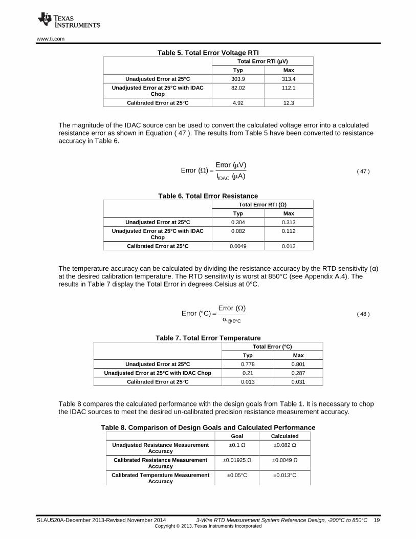
Table 5. Total Error Voltage RTI
The magnitude of the IDAC source can be used to convert the calculated voltage error into a calculated resistance error as shown in Equation ( 47 ). The results from Table 5 have been converted to resistance accuracy in Table 6.
)A(I
)V(Error)(Error
IDAC
( 47 )
Table 6. Total Error Resistance
The temperature accuracy can be calculated by dividing the resistance accuracy by the RTD sensitivity (α) at the desired calibration temperature. The RTD sensitivity is worst at 850°C (see Appendix A.4). The results in Table 7 display the Total Error in degrees Celsius at 0°C.
C0@
)(Error)C(Error
( 48 )
Table 7. Total Error Temperature
Table 8 compares the calculated performance with the design goals from Table 1. It is necessary to chop the IDAC sources to meet the desired un-calibrated precision resistance measurement accuracy.
Table 8. Comparison of Design Goals and Calculated Performance
Total Error RTI (μV)
Typ Max
Unadjusted Error at 25°C 303.9 313.4
Unadjusted Error at 25°C with IDAC Chop
82.02 112.1
Calibrated Error at 25°C 4.92 12.3
Total Error RTI (Ω)
Typ Max
Unadjusted Error at 25°C 0.304 0.313
Unadjusted Error at 25°C with IDAC Chop
0.082 0.112
Calibrated Error at 25°C 0.0049 0.012
Total Error (°C)
Typ Max
Unadjusted Error at 25°C 0.778 0.801
Unadjusted Error at 25°C with IDAC Chop 0.21 0.287
Calibrated Error at 25°C 0.013 0.031
Goal Calculated
Unadjusted Resistance Measurement Accuracy
±0.1 Ω ±0.082 Ω
Calibrated Resistance Measurement Accuracy
±0.01925 Ω ±0.0049 Ω
Calibrated Temperature Measurement Accuracy
±0.05°C ±0.013°C
www.ti.com
20 3-Wire RTD Measurement System Reference Design, -200°C to 850°C SLAU520A-December 2013-Revised November 2014 Copyright © 2013, Texas Instruments Incorporated
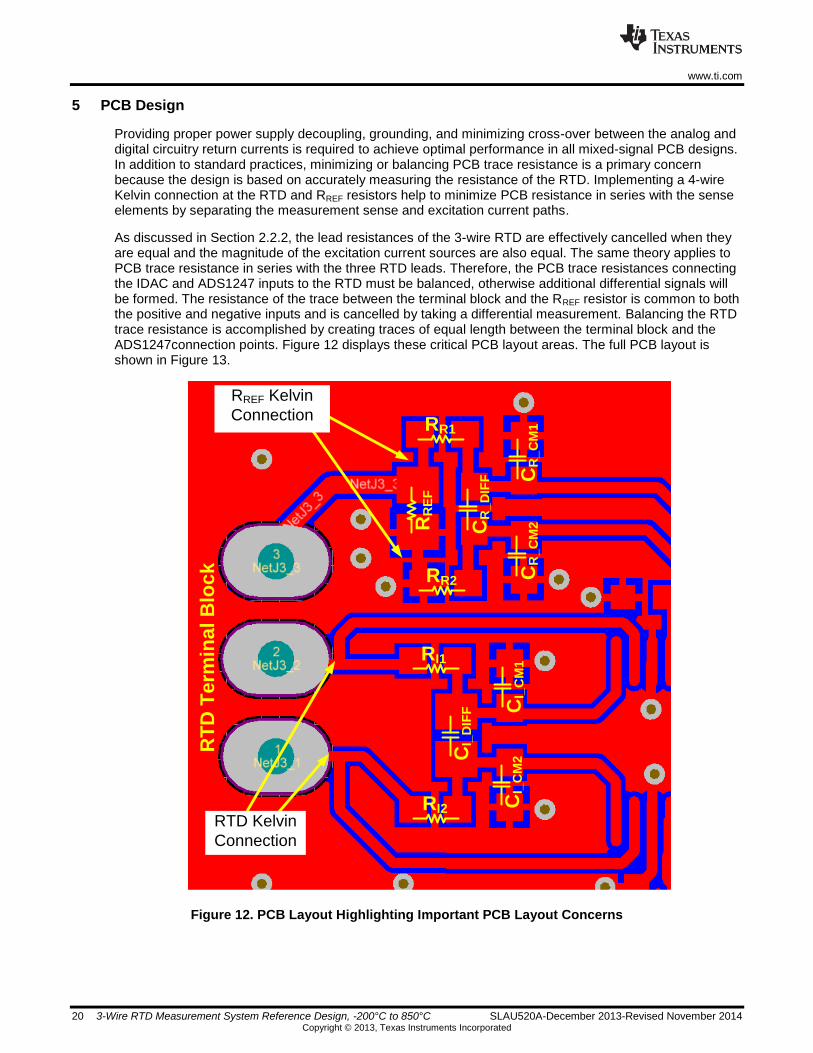
5 PCB Design
Providing proper power supply decoupling, grounding, and minimizing cross-over between the analog and digital circuitry return currents is required to achieve optimal performance in all mixed-signal PCB designs. In addition to standard practices, minimizing or balancing PCB trace resistance is a primary concern because the design is based on accurately measuring the resistance of the RTD. Implementing a 4-wire Kelvin connection at the RTD and RREF resistors help to minimize PCB resistance in series with the sense elements by separating the measurement sense and excitation current paths.
As discussed in Section 2.2.2, the lead resistances of the 3-wire RTD are effectively cancelled when they are equal and the magnitude of the excitation current sources are also equal. The same theory applies to PCB trace resistance in series with the three RTD leads. Therefore, the PCB trace resistances connecting the IDAC and ADS1247 inputs to the RTD must be balanced, otherwise additional differential signals will be formed. The resistance of the trace between the terminal block and the RREF resistor is common to both the positive and negative inputs and is cancelled by taking a differential measurement. Balancing the RTD trace resistance is accomplished by creating traces of equal length between the terminal block and the ADS1247connection points. Figure 12 displays these critical PCB layout areas. The full PCB layout is shown in Figure 13.
Figure 12. PCB Layout Highlighting Important PCB Layout Concerns
RREF Kelvin
Connection
RTD Kelvin
Connection
RR
EF
CR
_D
IFF
CR
_C
M2
CR
_C
M1
RI1
RI2
RR2
RR1
CI_
CM
2C
I_C
M1
CI_
DIF
F
RT
D T
erm
ina
l B
loc
k

www.ti.com
SLAU520A-December 2013-Revised November 2014 3-Wire RTD Measurement System Reference Design, -200°C to 850°C 21 Copyright © 2013, Texas Instruments Incorporated
Figure 13. Full PCB Layout
www.ti.com
22 3-Wire RTD Measurement System Reference Design, -200°C to 850°C SLAU520A-December 2013-Revised November 2014 Copyright © 2013, Texas Instruments Incorporated
6 Verification & Measured Performance
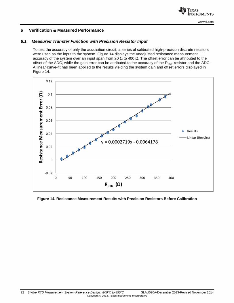
6.1 Measured Transfer Function with Precision Resistor Input
To test the accuracy of only the acquisition circuit, a series of calibrated high-precision discrete resistors were used as the input to the system. Figure 14 displays the unadjusted resistance measurement accuracy of the system over an input span from 20 Ω to 400 Ω. The offset error can be attributed to the offset of the ADC, while the gain error can be attributed to the accuracy of the RREF resistor and the ADC. A linear curve-fit has been applied to the results yielding the system gain and offset errors displayed in Figure 14.
Figure 14. Resistance Measurement Results with Precision Resistors Before Calibration
y = 0.0002719x - 0.0064178
-0.02
0
0.02
0.04
0.06
0.08
0.1
0.12
0 50 100 150 200 250 300 350 400
Re
sist
ance
Me
asu
rem
en
t Er
ror
(Ω)
RRTD (Ω)
Results
Linear (Results)

www.ti.com
SLAU520A-December 2013-Revised November 2014 3-Wire RTD Measurement System Reference Design, -200°C to 850°C 23 Copyright © 2013, Texas Instruments Incorporated
Precision temperature measurement applications are typically calibrated to remove the effects of gain and offset errors, which generally dominate the total system error. The simplest calibration method is a linear, or two-point, calibration which applies an equal and opposite gain and offset term to cancel the measured system gain and offset errors. Applying a gain and offset calibration yields the calibrated results shown in Figure 15. More information regarding calibration can be found in Reference 5.
Figure 15. Resistance Measurement Results with Precision Resistors after Calibration
The results in Figure 15 can be converted to temperature accuracy by dividing the results by the RTD sensitivity (α) at the measured resistance. Over the full resistance input range, the maximum total measured error is ±0.00415 Ω. Equation ( 49 ) uses this measurement and the RTD sensitivity at 0°C to calculate the measured temperature accuracy.
C0106.0
C39083.0
00415.0)(Error)C(Error
C0@
( 49 )
-0.01
-0.005
0
0.005
0.01
0 50 100 150 200 250 300 350 400
Re
sist
ance
Me
asu
rem
en
t Er
ror
(Ω)
RRTD (Ω)
Calibrated Results

www.ti.com
24 3-Wire RTD Measurement System Reference Design, -200°C to 850°C SLAU520A-December 2013-Revised November 2014 Copyright © 2013, Texas Instruments Incorporated
Figure 16 displays the calculated temperature accuracy of the circuit, not including any linearization related errors of the RTD.
Figure 16. Calculated Temperature Error from Resistance Measurement Error
-0.05
-0.0375
-0.025
-0.0125
0
0.0125
0.025
0.0375
0.05
0 50 100 150 200 250 300 350 400
Tem
pe
ratu
re E
rro
r (°
C)
RRTD (Ω)
Calibrated Results
www.ti.com
SLAU520A-December 2013-Revised November 2014 3-Wire RTD Measurement System Reference Design, -200°C to 850°C 25 Copyright © 2013, Texas Instruments Incorporated
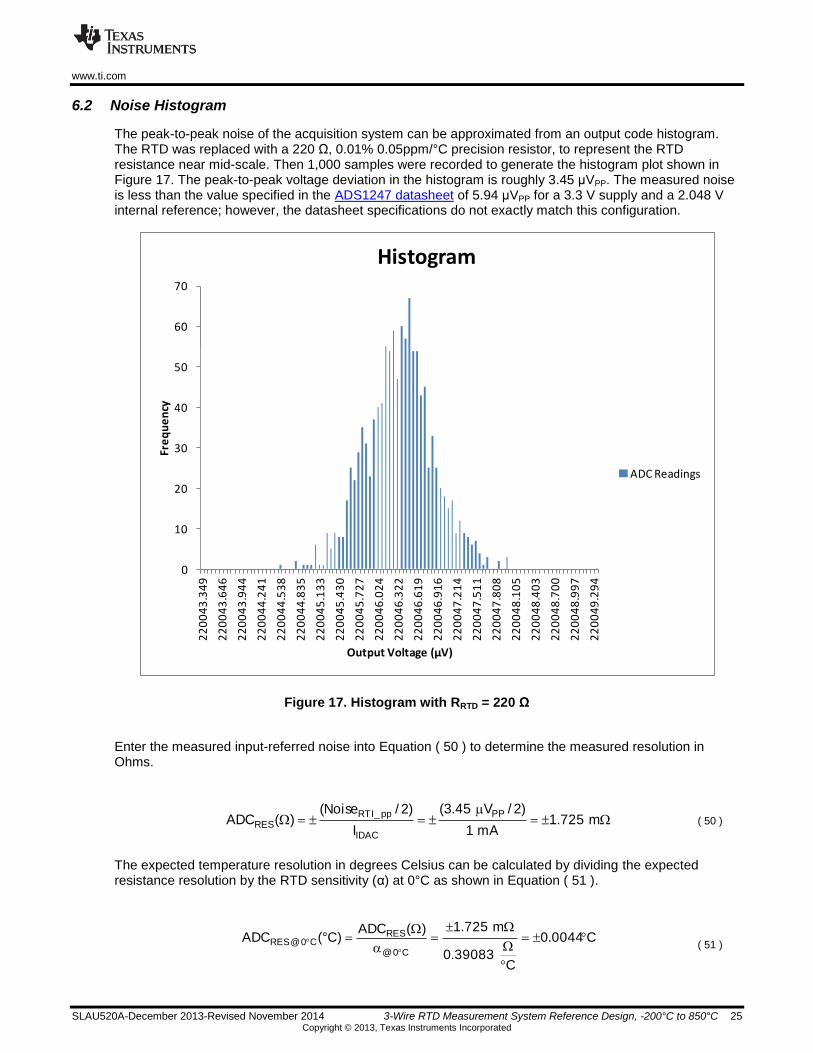
6.2 Noise Histogram
The peak-to-peak noise of the acquisition system can be approximated from an output code histogram. The RTD was replaced with a 220 Ω, 0.01% 0.05ppm/°C precision resistor, to represent the RTD resistance near mid-scale. Then 1,000 samples were recorded to generate the histogram plot shown in Figure 17. The peak-to-peak voltage deviation in the histogram is roughly 3.45 μVPP. The measured noise is less than the value specified in the ADS1247 datasheet of 5.94 μVPP for a 3.3 V supply and a 2.048 V internal reference; however, the datasheet specifications do not exactly match this configuration.
Figure 17. Histogram with RRTD = 220 Ω
Enter the measured input-referred noise into Equation ( 50 ) to determine the measured resolution in Ohms.
m725.1mA1
)2/V45.3(
I
)2/Noise()(ADC
PP
IDAC
pp_RTIRES ( 50 )
The expected temperature resolution in degrees Celsius can be calculated by dividing the expected resistance resolution by the RTD sensitivity (α) at 0°C as shown in Equation ( 51 ).
C0044.0
C39083.0
m725.1)(ADC)°C(ADC
C0@
RESC0@RES
( 51 )
0
10
20
30
40
50
60
70
22
00
43
.34
9
22
00
43
.64
6
22
00
43
.94
4
22
00
44
.24
1
22
00
44
.53
8
22
00
44
.83
5
22
00
45
.13
3
22
00
45
.43
0
22
00
45
.72
7
22
00
46
.02
4
22
00
46
.32
2
22
00
46
.61
9
22
00
46
.91
6
22
00
47
.21
4
22
00
47
.51
1
22
00
47
.80
8
22
00
48
.10
5
22
00
48
.40
3
22
00
48
.70
0
22
00
48
.99
7
22
00
49
.29
4
Fre
qu
en
cy
Output Voltage (µV)
Histogram
ADC Readings

www.ti.com
26 3-Wire RTD Measurement System Reference Design, -200°C to 850°C SLAU520A-December 2013-Revised November 2014 Copyright © 2013, Texas Instruments Incorporated
The temperature resolution falls well within the accuracy goal of ±0.05°C and can be observed in the results in Figure 16. The noise can be further reduced by applying additional averaging or filtering in software.
Table 9 compares the measured performance with the calculated performance and design goals from Table 8. It is necessary to chop the IDAC sources to meet the desired un-calibrated precision resistance measurement accuracy.
Table 9. Comparison of Design Goals, Calculated, and Measured Performance
7 Modifications
This design can be easily modified for other RTD types and temperature ranges by changing the IDAC, PGA, and RREF selections using the equations shown in the theory and component selection sections.
There are a few other fully integrated products available from TI that offer the same required building blocks as the ADS1247 but feature different performance, channel count, and cost. Several of these devices are listed in Table 10.
Table 10. Alternate Fully-Integrated ADC Solutions
ADC Resolution Differential Inputs
PGA Range IDACs Magnitude
Noise Power Consumption
ADS1147(1)
16 2 1 – 128 V/V 50 µA – 1.5 mA 15.63 µVRMS 1.4 mW
ADS1247(1)
24 2 1 – 128 V/V 50 µA – 1.5 mA 1.07 µVRMS 1.4 mW
ADS1148(1)
16 4 1 – 128 V/V 50 µA – 1.5 mA 15.63 µVRMS 1.4 mW
ADS1248(1)
24 4 1 – 128 V/V 50 µA – 1.5 mA 1.07 µVRMS 1.4 mW
ADS1120(1)
16 2 1 – 128 V/V 10 µA – 1.5 mA 15.63 µVRMS 1.4 mW
ADS1220(1)
24 2 1 – 128 V/V 10 µA – 1.5 mA 1.15 µVRMS 1.4 mW
LMP90100(2)
24 4 1 – 128 V/V 100 µA – 1 mA 4.29 µVRMS 5.1 mW
(1)
AVDD = 3.3 V, AVSS = 0 V, Internal Reference = 2.048 V, Data Rate = 20 SPS, PGA = 4 V/V
(2)
AVDD = 3 V, AVSS = 0 V, Internal Reference = 3 V, Data Rate = 13.42 SPS, PGA = 4 V/V
Table 11 features other suitable ADC solutions that offer integrated PGAs.
Table 11. Alternate ADC + PGA Solutions
ADC Resolution Differential Inputs
PGA Range Noise Power Consumption
ADS1146(1)
16 1 1 – 128 V/V 15.63 µVRMS 1.4 mW
ADS1246(1)
24 1 1 – 128 V/V 1.07 µVRMS 1.4 mW
LMP90099(2)
24 4 1 – 128 V/V 4.29 µVRMS 5.1 mW
(1)
AVDD = 3.3 V, AVSS = 0 V, Internal Reference = 2.048 V, Data Rate = 20 SPS, PGA = 4 V/V
(2)
AVDD = 3 V, AVSS = 0 V, Internal Reference = 3 V, Data Rate = 13.42 SPS, PGA = 4 V/V
Discrete current sources could be comprised of an integrated device such as the REF200 or a circuit such as the designs featured in TIPD101 or TIPD107.
Goal Calculated Measured
Unadjusted Resistance Measurement Accuracy
±0.1 Ω ±0.082 Ω ±0.096 Ω
Calibrated Resistance Measurement Accuracy
±0.01925 Ω ±0.0049 Ω ±0.00415 Ω
Calibrated Temperature Measurement Accuracy
±0.05°C ±0.013°C ±0.0106°C

www.ti.com
SLAU520A-December 2013-Revised November 2014 3-Wire RTD Measurement System Reference Design, -200°C to 850°C 27 Copyright © 2013, Texas Instruments Incorporated
8 About the Authors
Ryan Andrews is an applications engineer with the Precision Analog Delta-Sigma ADC team at Texas Instruments, where he supports industrial and medical products and applications. Ryan received his BS in Biomedical Engineering and his BA in Spanish from the University of Rhode Island.
Collin Wells is an applications engineer in the Precision Linear group at Texas Instruments where he supports industrial products and applications. Collin received his BSEE from the University of Texas, Dallas.
9 Acknowledgements & References
1. Luis Chioye, “RTD Ratiometric Measurement and Filtering Using the ADS1148 and ADS1248 Family of Devices” SBAA201, March 2013.
2. Robert Burnham and Nagaraj Ananthapadamanabhan, “Example Temperature Measurement Applications Using the ADS1247 and ADS1248” SBAA180, January 2011.
3. Collin Wells, “Signal Conditioning and Linearization of RTD Sensors” 2011 Texas Instruments Technology Day Presentation.
4. Omega ®, “The Omega ® Temperature Measurement HandbookTM
and Encyclopedia, Vol MMXIV
TM, 7
th Edition.
5. Mock, Mike, 0-1A, Single-Supply, Low-Side, Current Sensing Solution, TIDU040

www.ti.com
28 3-Wire RTD Measurement System Reference Design, -200°C to 850°C SLAU520A-December 2013-Revised November 2014 Copyright © 2013, Texas Instruments Incorporated
Appendix A.
A.1 Electrical Schematic
Figure 18. Electrical Schematic

www.ti.com
SLAU520A-December 2013-Revised November 2014 3-Wire RTD Measurement System Reference Design, -200°C to 850°C 29 Copyright © 2013, Texas Instruments Incorporated
A.2 Bill of Materials
Figure 19. Bill of Materials
www.ti.com
30 3-Wire RTD Measurement System Reference Design, -200°C to 850°C SLAU520A-December 2013-Revised November 2014 Copyright © 2013, Texas Instruments Incorporated
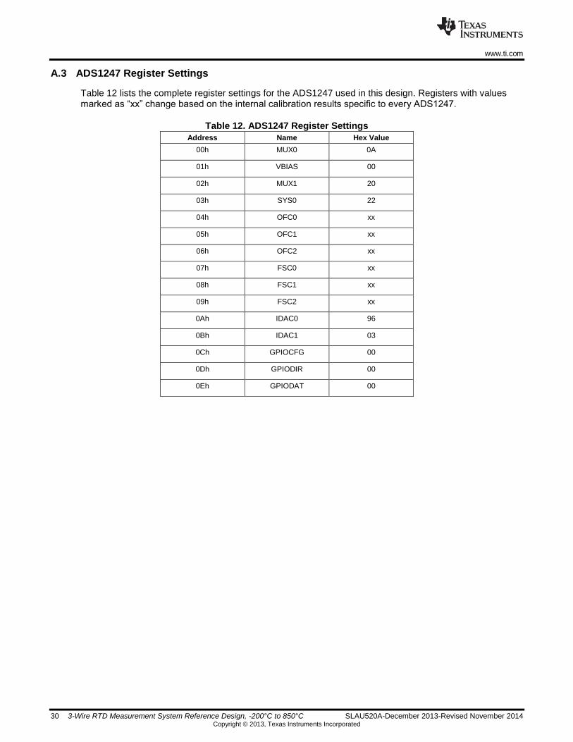
A.3 ADS1247 Register Settings
Table 12 lists the complete register settings for the ADS1247 used in this design. Registers with values marked as “xx” change based on the internal calibration results specific to every ADS1247.
Table 12. ADS1247 Register Settings
Address Name Hex Value
00h MUX0 0A
01h VBIAS 00
02h MUX1 20
03h SYS0 22
04h OFC0 xx
05h OFC1 xx
06h OFC2 xx
07h FSC0 xx
08h FSC1 xx
09h FSC2 xx
0Ah IDAC0 96
0Bh IDAC1 03
0Ch GPIOCFG 00
0Dh GPIODIR 00
0Eh GPIODAT 00
www.ti.com
SLAU520A-December 2013-Revised November 2014 3-Wire RTD Measurement System Reference Design, -200°C to 850°C 31 Copyright © 2013, Texas Instruments Incorporated
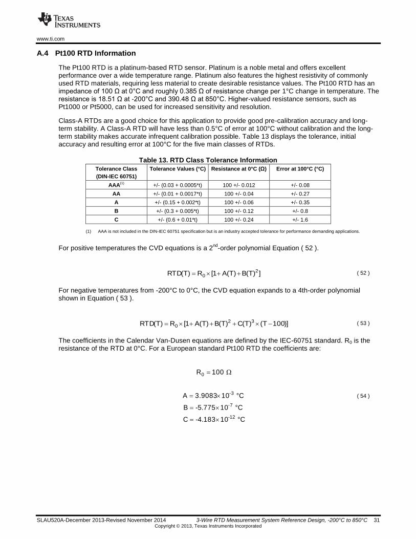
A.4 Pt100 RTD Information
The Pt100 RTD is a platinum-based RTD sensor. Platinum is a noble metal and offers excellent performance over a wide temperature range. Platinum also features the highest resistivity of commonly used RTD materials, requiring less material to create desirable resistance values. The Pt100 RTD has an impedance of 100 Ω at 0°C and roughly 0.385 Ω of resistance change per 1°C change in temperature. The resistance is 18.51 Ω at -200°C and 390.48 Ω at 850°C. Higher-valued resistance sensors, such as Pt1000 or Pt5000, can be used for increased sensitivity and resolution.
Class-A RTDs are a good choice for this application to provide good pre-calibration accuracy and long-term stability. A Class-A RTD will have less than 0.5°C of error at 100°C without calibration and the long-term stability makes accurate infrequent calibration possible. Table 13 displays the tolerance, initial accuracy and resulting error at 100°C for the five main classes of RTDs.
Table 13. RTD Class Tolerance Information
Tolerance Class
(DIN-IEC 60751)
Tolerance Values (°C) Resistance at 0°C (Ω) Error at 100°C (°C)
AAA(1)
+/- (0.03 + 0.0005*t) 100 +/- 0.012 +/- 0.08
AA +/- (0.01 + 0.0017*t) 100 +/- 0.04 +/- 0.27
A +/- (0.15 + 0.002*t) 100 +/- 0.06 +/- 0.35
B +/- (0.3 + 0.005*t) 100 +/- 0.12 +/- 0.8
C +/- (0.6 + 0.01*t) 100 +/- 0.24 +/- 1.6
(1)
AAA is not included in the DIN-IEC 60751 specification but is an industry accepted tolerance for performance demanding applications.
For positive temperatures the CVD equations is a 2nd
-order polynomial Equation ( 52 ).
])T(B)T(A1[R)T(RTD 20 ( 52 )
For negative temperatures from -200°C to 0°C, the CVD equation expands to a 4th-order polynomial shown in Equation ( 53 ).
)]100T()T(C)T(B)T(A1[R)T(RTD 320 ( 53 )
The coefficients in the Calendar Van-Dusen equations are defined by the IEC-60751 standard. R0 is the resistance of the RTD at 0°C. For a European standard Pt100 RTD the coefficients are:
°C10 183.4-C
°C10 775.5-B
°C10 3.9083A
100R
12-
7-
3-
0
( 54 )

www.ti.com
32 3-Wire RTD Measurement System Reference Design, -200°C to 850°C SLAU520A-December 2013-Revised November 2014 Copyright © 2013, Texas Instruments Incorporated
The change in resistance of a Pt100 RTD from -200°C to 850°C is displayed in Figure 20.
Figure 20. Pt100 RTD Resistance from -200°C to 850°C
While the change in RTD resistance is fairly linear over small temperature ranges, Figure 21 displays the resulting non-linearity if an end-point fit is made to the curve shown in Figure 20. The results show almost 4.5% non-linearity, or greater than 16°C, illustrating the need for digital calibration.
Figure 21. Pt100 RTD Non-Linearity from -200°C to 850°C
200 95 10 115 220 325 430 535 640 745 8500
40
80
120
160
200
240
280
320
360
400
PT-100 RTD Resistance vs. Temperature
Temperature (C)
Res
ista
nce
(O
hm
s)
RTD Temp( )
Temp
200 95 10 115 220 325 430 535 640 745 8500
2
4
6
8
10
12
14
16
18
20
0
0.5
1
1.5
2
2.5
3
3.5
4
4.5
5
Resistance Error and Nonlinearity %FSR
Temperature (C)
Res
ista
nce
Err
or
(Ohm
s)
Res
ista
nce
Non
linea
rity
(%
)NonlinOhms Temp( ) NonlinError Temp( )
Temp
www.ti.com
SLAU520A-December 2013-Revised November 2014 3-Wire RTD Measurement System Reference Design, -200°C to 850°C 33 Copyright © 2013, Texas Instruments Incorporated
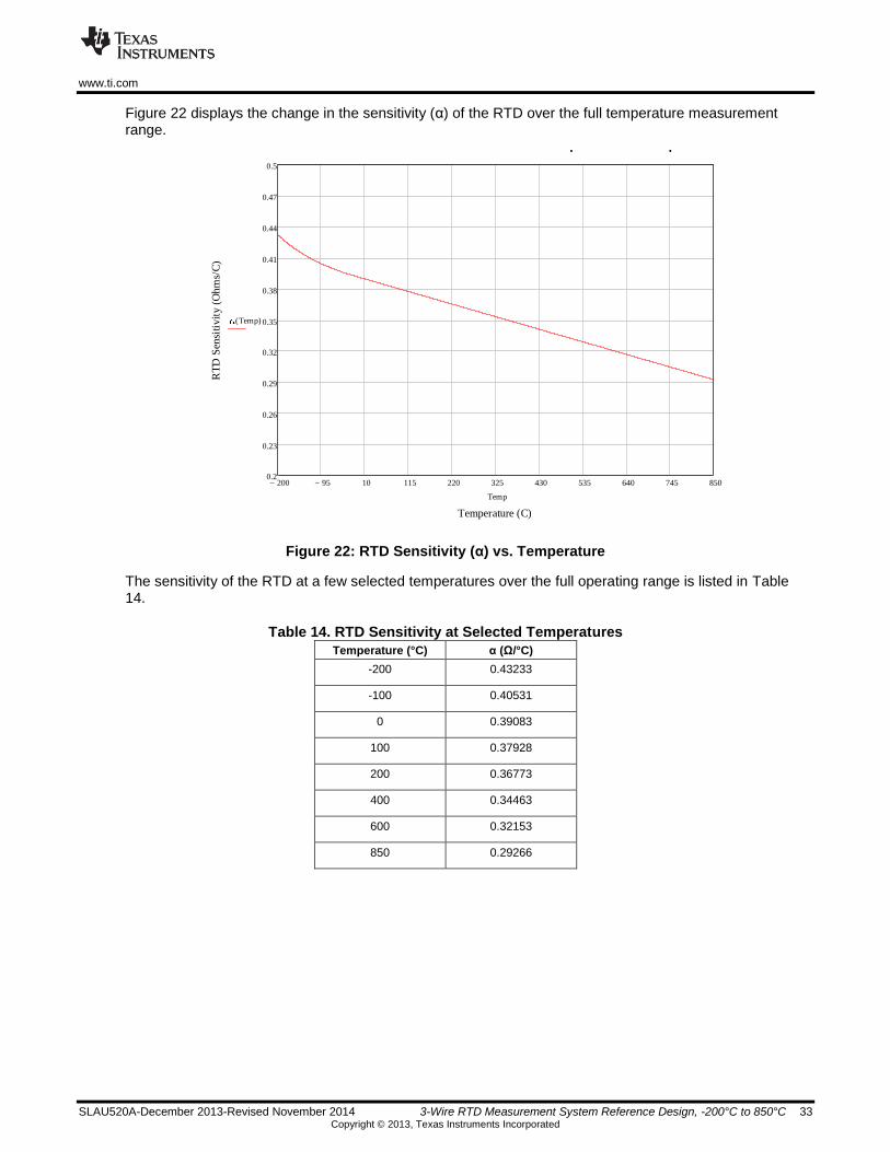
Figure 22 displays the change in the sensitivity (α) of the RTD over the full temperature measurement range.
Figure 22: RTD Sensitivity (α) vs. Temperature
The sensitivity of the RTD at a few selected temperatures over the full operating range is listed in Table 14.
Table 14. RTD Sensitivity at Selected Temperatures
Temperature (°C) α (Ω/°C)
-200 0.43233
-100 0.40531
0 0.39083
100 0.37928
200 0.36773
400 0.34463
600 0.32153
850 0.29266
Plot Difference Between RTD Resistance and a Linear Endpoint Fit vs. Temperature
200 95 10 115 220 325 430 535 640 745 8500.2
0.23
0.26
0.29
0.32
0.35
0.38
0.41
0.44
0.47
0.5
Temperature (C)
RT
D S
ensi
tiv
ity
(O
hm
s/C
)
Temp( )
Temp

www.ti.com
34 3-Wire RTD Measurement System Reference Design, -200°C to 850°C SLAU520A-December 2013-Revised November 2014 Copyright © 2013, Texas Instruments Incorporated
A.5 Error Calculations Including Temperature Drift
The calculations shown in this section are provided in supplement to the room temperature calculations shown in Section 4.2.2. The calculations are performed over an operating temperature range of -40°C to +85°C. The largest errors due to temperature drift occur at the operating temperature furthest from the ambient temperature of 25°C as shown in Equation ( 55 ).
C65)C40(C25TMAX ( 55 )
A.5.1 Errors caused by RREF Temperature Drift
The RREF drift specification must be multiplied by the temperature change and converted to a percentage before performing the same calculations used for the RREF tolerance.
C
ppm2
C
ppmR DriftREF
( 56 )
ppm130C65C
ppm2T
C
ppmR)ppm(R MAXDriftREFDriftREF
( 57 )
%013.0100000,000,1
130100
000,000,1
)ppm(R(%)R
DriftREF
DriftREF ( 58 )
%01299.0100100013.0
013.0100
100(%)R
(%)R(%)ErrorGain
DriftREF
DriftREF
DriftRREF
( 59 )
The error in volts due to the RREF drift can be calculated by multiplying the gain error in percent by VIN_MAX.
V7234.50)V(ErrorGain
mV48.390100
01299.0V
100
(%)ErrorGain)V(ErrorGain
DriftREF
DriftREF
DriftREF
R
MAX_IN
R
R
( 60 )
A.5.2 Errors due to ADS1247 Temperature Drift
As the ambient temperature changes, the ADS1247 will produce errors due to offset drift, gain error drift, and IDAC mismatch drift.
Offset error drift is commonly specified as an input-referred voltage and can be directly entered from the device performance datasheet. The largest offset drift error will be at a system ambient temperature of -40°C (See Figure 15 in the ADS1247 datasheet).
V1)V(ErrorOffset DriftADC ( 61 )
www.ti.com
SLAU520A-December 2013-Revised November 2014 3-Wire RTD Measurement System Reference Design, -200°C to 850°C 35 Copyright © 2013, Texas Instruments Incorporated
If offset drift is specified in μV/°C then it will first be multiplied by ∆TMAX to determine the final offset voltage due to temperature drift.
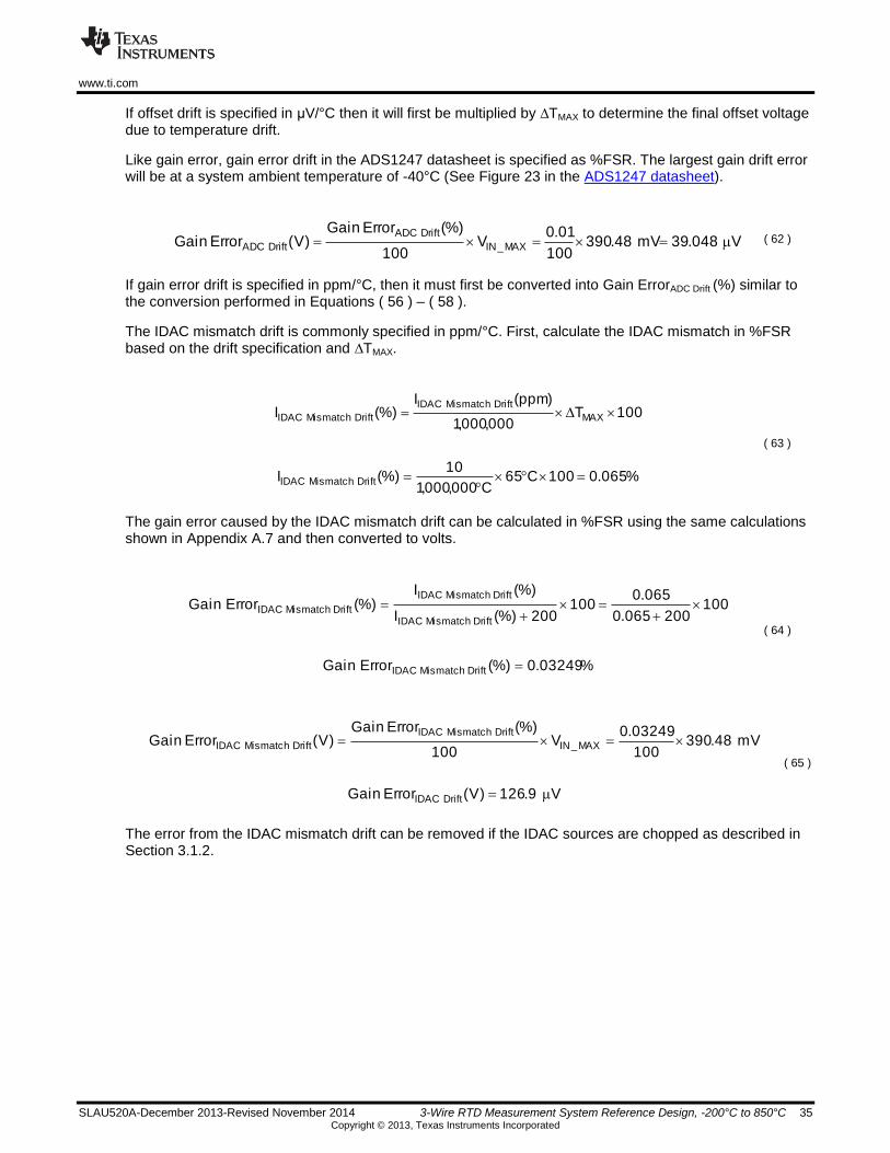
Like gain error, gain error drift in the ADS1247 datasheet is specified as %FSR. The largest gain drift error will be at a system ambient temperature of -40°C (See Figure 23 in the ADS1247 datasheet).
V048.39mV48.390100
01.0V
100
(%)ErrorGain)V(ErrorGain MAX_IN
DriftADC
DriftADC ( 62 )
If gain error drift is specified in ppm/°C, then it must first be converted into Gain ErrorADC Drift (%) similar to the conversion performed in Equations ( 56 ) – ( 58 ).
The IDAC mismatch drift is commonly specified in ppm/°C. First, calculate the IDAC mismatch in %FSR based on the drift specification and ∆TMAX.
%065.0100C65C000,000,1
10(%)I
100T000,000,1
)ppm(I(%)I
DriftMismatchIDAC
MAX
DriftMismatchIDAC
DriftMismatchIDAC
( 63 )
The gain error caused by the IDAC mismatch drift can be calculated in %FSR using the same calculations shown in Appendix A.7 and then converted to volts.
%03249.0(%)ErrorGain
100200065.0
065.0100
200(%)I
(%)I(%)ErrorGain
DriftMismatchIDAC
DriftMismatchIDAC
DriftMismatchIDAC
DriftMismatchIDAC
( 64 )
V9.126)V(ErrorGain
mV48.390100
03249.0V
100
(%)ErrorGain)V(ErrorGain
DriftIDAC
MAX_IN
DriftMismatchIDAC
DriftMismatchIDAC
( 65 )
The error from the IDAC mismatch drift can be removed if the IDAC sources are chopped as described in Section 3.1.2.
www.ti.com
36 3-Wire RTD Measurement System Reference Design, -200°C to 850°C SLAU520A-December 2013-Revised November 2014 Copyright © 2013, Texas Instruments Incorporated
A.5.3 Total Error over Temperature
With all of the input-referred errors calculated in volts, the total error can be calculated by taking the root-sum-of-square of all of the uncorrelated ambient temperature and temperature drift error terms.
V9.303)V(Error
ErrorGainErrorGainErrorINL
ErrorGainErrorGainErrorOffset
ErrorOffsetErrorGainErrorGain
)V(Error
Total
2DriftMismatchIDAC
2IDAC
2ADC
2DriftADC
2ADC
2DriftADC
2ADC
2DriftTolR
2TolR
Total
REFREF
( 66 )
The system errors over temperature and their resulting input-referred errors in μV are summarized in Table 15.
Table 15. Summary of Error Sources and Resulting Voltage Error RTI over Temperature
The IDAC mismatch errors can be removed by chopping the IDAC sources as described in Section 3.1.2. A two-point gain and offset calibration can remove the errors from the RREF tolerance, offset voltage, gain error, and IDAC mismatch leaving only the error from INL and temperature drift errors. Table 16 compares the unadjusted error with the error after chopping the IDAC sources and performing a two-point gain and offset calibration at 25°C and over temperature.
Table 16. Total Error Voltage RTI over Operating Temperature
Error Source Value Input-Referred Error (μV)
Typ Max Typ Max
RREF Errors
RREF Tolerance - 0.02% - 164
RREF Drift - 2 ppm/°C - 106.6
ADS1247 Errors
Integrated Nonlinearity (INL) 6 ppm 15 ppm 4.92 12.3
Offset Voltage - 15 μV - 15
Offset Voltage Drift 1 μV 1
Gain Error 0.005% 0.02% 19.52 78.1
Gain Error Drift 0.01% 0.015% 39.05 58.57
IDAC Mismatch - 0.15% - 292.6
IDAC Mismatch Drift - 10 ppm/°C - 126.9
Total Error (μV)
Typ Max
Unadjusted Error at 25°C 303.9 313.4
Unadjusted Error at 25°C with IDAC Chop 82.02 112.1
Calibrated Error at 25°C 4.92 12.3
Unadjusted Error over Temp 335.5 346.9
Unadjusted Error over Temp with IDAC Chop 104.1 136.3
Calibrated Error over Temp 142.2 149.2
Calibrated Error over Temp with IDAC Chop 64.2 78.5

www.ti.com
SLAU520A-December 2013-Revised November 2014 3-Wire RTD Measurement System Reference Design, -200°C to 850°C 37 Copyright © 2013, Texas Instruments Incorporated
The magnitude of the IDAC source can be used to convert the calculated voltage error into a calculated resistance error in Ohms as shown in Equation ( 47 ). The results from Table 16 have been converted to resistance accuracy in Table 17.
Table 17. Total Resistance Error over Operating Temperature
With the resistance accuracy known, the final temperature accuracy can be calculated by dividing the resistance accuracy by the change in the RTD resistance per degree Celsius. The results in Table 18 use the sensitivity at 0°C of 0.3908Ω/°C.
Table 18. Total Temperature Error over Operating Temperature
A.6 Derivation of the Errors from RREF Tolerance
The ideal transfer function will be compared to a modified transfer function to determine the effects of RREF tolerance on the system accuracy. The ideal transfer function is shown again in Equation ( 67 ).
REF
RTDTOTALIDEAL
R4
RCodesCode ( 67 )
If RREF is substituted with (RREF+RREF*∆) in the ideal transfer function, then it simplifies to Equation ( 68 ).
REFREF
RTDTOTALErrorR
RR4
RCodesCode
REF ( 68 )
Equation ( 69 ) calculates the gain error caused by the RREF tolerance by comparing the calculated error transfer function to the ideal transfer function.
1Code
CodeCode(%)ErrorGain
IDEAL
IDEALErrorR
TolRREF
REF
( 69 )
Total Error (Ω)
Typ Max
Unadjusted Error at 25°C 0.304 0.313
Unadjusted Error at 25°C with IDAC Chop 0.082 0.112
Calibrated Error at 25°C 0.0049 0.012
Unadjusted Error over Temp 0.335 0.347
Unadjusted Error over Temp with IDAC Chop 0.104 0.136
Calibrated Error over Temp 0.142 0.149
Calibrated Error over Temp with IDAC Chop 0.064 0.079
Total Error (°C)
Typ Max
Unadjusted Error at 25°C 0.778 0.802
Unadjusted Error at 25°C with IDAC Chop 0.21 0.287
Calibrated Error at 25°C 0.013 0.031
Unadjusted Error over Temp 0.858 0.887
Unadjusted Error over Temp with IDAC Chop 0.266 0.349
Calibrated Error over Temp 0.364 0.382
Calibrated Error over Temp with IDAC Chop 0.164 0.201
www.ti.com
38 3-Wire RTD Measurement System Reference Design, -200°C to 850°C SLAU520A-December 2013-Revised November 2014 Copyright © 2013, Texas Instruments Incorporated
If RREF is substituted with RREF-RREF*∆ to calculate the effects of a decrease in RREF, the polarity of the gain error will be positive.
Assuming the tolerance is specified in %, the gain error can be calculated as shown:
100(%)R
(%)R(%)ErrorGain
TolREF
TolREF
TolRREF ( 70 )
A.7 Derivation of the Errors from IDAC Mismatch
The ideal transfer function will be compared to a modified transfer function to determine the effects of a mismatch in the IDAC current sources on the system accuracy. The ideal transfer function is shown again in Equation ( 71 ).
REF
RTDTOTALIDEAL
R4
RCodesCode ( 71 )
However, if I2 is set equal to (I1+ I1*∆) in Equation ( 7 ), the transfer function simplifies to Equation ( 72 ).
2R4
RCodesCode
REF
RTDTOTALErrorMismatchIDAC ( 72 )
Equation ( 73 ) calculates the gain error caused by the IDAC mismatch by comparing the calculated error transfer function to the ideal transfer function.
2Code
CodeCode(%)ErrorGain
IDEAL
IDEALErrorMismatchIDAC
DriftMismatchIDAC
( 73 )
If I1 is substituted with I2+ I2*∆, the polarity of the gain error will be positive.
Assuming the IDAC mismatch is specified in %FSR, the gain error can be calculated as shown in Equation ( 74 ).
200(%)I
(%)I(%)ErrorGain
DriftMismatchIDAC
DriftMismatchIDAC
DriftMismatchIDAC
( 74 )

IMPORTANT NOTICE FOR TI REFERENCE DESIGNSTexas Instruments Incorporated ("TI") reference designs are solely intended to assist designers (“Buyers”) who are developing systems thatincorporate TI semiconductor products (also referred to herein as “components”). Buyer understands and agrees that Buyer remainsresponsible for using its independent analysis, evaluation and judgment in designing Buyer’s systems and products.TI reference designs have been created using standard laboratory conditions and engineering practices. TI has not conducted anytesting other than that specifically described in the published documentation for a particular reference design. TI may makecorrections, enhancements, improvements and other changes to its reference designs.Buyers are authorized to use TI reference designs with the TI component(s) identified in each particular reference design and to modify thereference design in the development of their end products. HOWEVER, NO OTHER LICENSE, EXPRESS OR IMPLIED, BY ESTOPPELOR OTHERWISE TO ANY OTHER TI INTELLECTUAL PROPERTY RIGHT, AND NO LICENSE TO ANY THIRD PARTY TECHNOLOGYOR INTELLECTUAL PROPERTY RIGHT, IS GRANTED HEREIN, including but not limited to any patent right, copyright, mask work right,or other intellectual property right relating to any combination, machine, or process in which TI components or services are used.Information published by TI regarding third-party products or services does not constitute a license to use such products or services, or awarranty or endorsement thereof. Use of such information may require a license from a third party under the patents or other intellectualproperty of the third party, or a license from TI under the patents or other intellectual property of TI.TI REFERENCE DESIGNS ARE PROVIDED "AS IS". TI MAKES NO WARRANTIES OR REPRESENTATIONS WITH REGARD TO THEREFERENCE DESIGNS OR USE OF THE REFERENCE DESIGNS, EXPRESS, IMPLIED OR STATUTORY, INCLUDING ACCURACY ORCOMPLETENESS. TI DISCLAIMS ANY WARRANTY OF TITLE AND ANY IMPLIED WARRANTIES OF MERCHANTABILITY, FITNESSFOR A PARTICULAR PURPOSE, QUIET ENJOYMENT, QUIET POSSESSION, AND NON-INFRINGEMENT OF ANY THIRD PARTYINTELLECTUAL PROPERTY RIGHTS WITH REGARD TO TI REFERENCE DESIGNS OR USE THEREOF. TI SHALL NOT BE LIABLEFOR AND SHALL NOT DEFEND OR INDEMNIFY BUYERS AGAINST ANY THIRD PARTY INFRINGEMENT CLAIM THAT RELATES TOOR IS BASED ON A COMBINATION OF COMPONENTS PROVIDED IN A TI REFERENCE DESIGN. IN NO EVENT SHALL TI BELIABLE FOR ANY ACTUAL, SPECIAL, INCIDENTAL, CONSEQUENTIAL OR INDIRECT DAMAGES, HOWEVER CAUSED, ON ANYTHEORY OF LIABILITY AND WHETHER OR NOT TI HAS BEEN ADVISED OF THE POSSIBILITY OF SUCH DAMAGES, ARISING INANY WAY OUT OF TI REFERENCE DESIGNS OR BUYER’S USE OF TI REFERENCE DESIGNS.TI reserves the right to make corrections, enhancements, improvements and other changes to its semiconductor products and services perJESD46, latest issue, and to discontinue any product or service per JESD48, latest issue. Buyers should obtain the latest relevantinformation before placing orders and should verify that such information is current and complete. All semiconductor products are soldsubject to TI’s terms and conditions of sale supplied at the time of order acknowledgment.TI warrants performance of its components to the specifications applicable at the time of sale, in accordance with the warranty in TI’s termsand conditions of sale of semiconductor products. Testing and other quality control techniques for TI components are used to the extent TIdeems necessary to support this warranty. Except where mandated by applicable law, testing of all parameters of each component is notnecessarily performed.TI assumes no liability for applications assistance or the design of Buyers’ products. Buyers are responsible for their products andapplications using TI components. To minimize the risks associated with Buyers’ products and applications, Buyers should provideadequate design and operating safeguards.Reproduction of significant portions of TI information in TI data books, data sheets or reference designs is permissible only if reproduction iswithout alteration and is accompanied by all associated warranties, conditions, limitations, and notices. TI is not responsible or liable forsuch altered documentation. Information of third parties may be subject to additional restrictions.Buyer acknowledges and agrees that it is solely responsible for compliance with all legal, regulatory and safety-related requirementsconcerning its products, and any use of TI components in its applications, notwithstanding any applications-related information or supportthat may be provided by TI. Buyer represents and agrees that it has all the necessary expertise to create and implement safeguards thatanticipate dangerous failures, monitor failures and their consequences, lessen the likelihood of dangerous failures and take appropriateremedial actions. Buyer will fully indemnify TI and its representatives against any damages arising out of the use of any TI components inBuyer’s safety-critical applications.In some cases, TI components may be promoted specifically to facilitate safety-related applications. With such components, TI’s goal is tohelp enable customers to design and create their own end-product solutions that meet applicable functional safety standards andrequirements. Nonetheless, such components are subject to these terms.No TI components are authorized for use in FDA Class III (or similar life-critical medical equipment) unless authorized officers of the partieshave executed an agreement specifically governing such use.Only those TI components that TI has specifically designated as military grade or “enhanced plastic” are designed and intended for use inmilitary/aerospace applications or environments. Buyer acknowledges and agrees that any military or aerospace use of TI components thathave not been so designated is solely at Buyer's risk, and Buyer is solely responsible for compliance with all legal and regulatoryrequirements in connection with such use.TI has specifically designated certain components as meeting ISO/TS16949 requirements, mainly for automotive use. In any case of use ofnon-designated products, TI will not be responsible for any failure to meet ISO/TS16949.
Mailing Address: Texas Instruments, Post Office Box 655303, Dallas, Texas 75265Copyright © 2014, Texas Instruments Incorporated