2017 International Electrostatic Discharge Workshop
21
11th International Electrostatic Discharge Workshop May 7-11, 2017 Granlibakken Conference Center & Lodge, Tahoe City, California, USA IEW Setting the Global Standards for Static Control! EOS/ESD Association, Inc. 7900 Turin Rd., Bldg. 3 Rome, NY 13440-2069, USA PH +1-315-339-6937 • Email: [email protected] • www.esda.org
-
Upload
eosesd-association -
Category
Education
-
view
58 -
download
1
Transcript of 2017 International Electrostatic Discharge Workshop
11th International Electrostatic Discharge Workshop
May 7-11, 2017 Granlibakken Conference Center & Lodge, Tahoe City, California, USA
IEW
Setting the Global Standards for Static Control! EOS/ESD Association, Inc. 7900 Turin Rd., Bldg. 3 Rome, NY 13440-2069, USA
PH +1-315-339-6937 • Email: [email protected] • www.esda.org

1
Management Committee: Management Committee Chair: Hans Kunz, Texas Instruments, Inc.Technical Program Chair: Souvick Mitra, GLOBALFOUNDRIESSeminar Chair: Junjun Li, IBMInvited Speaker Co-Chairs: Stephen Fairbanks, SRF Technologies, LLC Michael Khazhinsky, Silicon Laboratories, Inc.Discussion Groups/Special Interest Groups Co-Chairs:Tom Meuse, Thermo Fisher ScientificEugene Worley, Qualcomm, Inc.Keynote Speaker Chair:Charvaka Duvvury, ESD Consulting LLCAudio/Visual Chair:Scott Ruth, NXP SemiconductorsIndustry Council Advisor: Charvaka Duvvury, ESD Consulting LLCESDA Events Director:Alan Righter, Analog Devices, Inc.ESDA HQ Executive Director:Lisa PimpinellaESDA HQ Chair:Christina Earl
The International ESD Workshop (IEW) hosts its 11th annual event at the majestic Granlibakken Conference Center & Lodge, Tahoe City, CA. Located in beautiful Tahoe City, this setting provides the perfect opportunity for participants to meet in a relaxed, invigorating atmosphere and engage in discussions about the latest research and issues of interest within the EOS/ESD community.
The IEW facilitates access to and interactions with industry leaders through invited seminars, technical sessions, special interest groups (SIGs), discussion groups (DGs), and invited speakers. This year we focus on The Intersection of ESD Challenges for Emerging/Advancing Technologies and Markets, IC Designer’s Perspective on ESD, and Everything EOS – Product, Failure Analysis, Reliability, Verification, and Test Engineers.
Experience the uniquely interactive program of the IEW Workshop.• Listen to viewpoints of industry experts• Share your ideas and opinions on EOS/ESD topics• Explore industry best practices and give your inputs• Interact and network with high-level EOS/ESD industry experts
A highly rewarding and engaging experience for all! Whether you are new to EOS/ESD topics, or an old hand at it - join us at IEW 2017 to learn in an informal, interactive, and friendly atmosphere.
A highly rewarding experience!
IEW 2016 Poster Session, Evangelische Akademie, Tutzing, Germany
Technical Program Committee:Fabrice Blanc, ARM Brett Carn, IntelLorenzo Cerati, STMicroelectronicsMichael Chaine, Micron Technology James DiSarro, Texas Instruments, Inc.Alaine Loiseau, IBMMarkus Mergens, QPX GmbH Manjunatha Prabhu, GLOBALFOUNDRIESAkram Salman, Texas Instruments, Inc.Mirko Scholz, imec Vladislav Vashchenko, Maxim Integrated Corp.Heinrich Wolf, Fraunhofer IZM Eugene Worley, Qualcomm, Inc.

2
Greetings from the 11th annual International ESD Workshop (IEW) Management Team! This event presents a unique opportunity for attendees to participate in in-depth discussions and learning on EOS and ESD topics in a highly interactive environment. Part of the interactive environment comes from the event location, itself. This event will be held at the Granlibakken Resort, nestled in a picturesque mountain valley, just minutes away from Lake Tahoe.
The settings and facilities of this location encourage immersive interaction and stimulating discussions. Focused discussion groups (DGs), held in the evenings, are a unique part of our interactive workshop. While each EOS/ESD topic discussion is facilitated by an expert on the subject, the main discussion will take place among the DG participants. The DGs will address topics of the focus issues and include ESD SPICE modeling, 3D-IC, IEC and CDM testing, system-level ESD design, device AMR considerations for EOS, and automotive EOS and reliability.
Scheduled poster sessions form the core of the technical program. These poster sessions begin with a brief introduction of each poster by the authors in a plenary “teaser” session. These teasers encourage the participants to visit each poster and its author in the subsequent interactive poster discussion session. To compliment the offering, attendees are also encouraged to bring open posters. This format provides an ideal forum for learning and the interchange of new ideas. Topics covered in the poster sessions include IC EOS/ESD design, testing, latch-up, TCAD, FINFET ESD design, and system level ESD.
The IEW also provides a forum for interactive special interest groups (SIGs), on selected subjects that may extend beyond the IEW time frame. Some SIGs have been successfully meeting for several years.
A number of stimulating state-of-the-art EOS/ESD seminars, as well as invited talks are scheduled. Come and listen to presentations, and later meet with the presenters, discussing advanced IC interconnects, ESD SPICE modeling, on-chip ESD and EOS detectors, the IoT, and other exciting topics.
As a break to EOS/ESD discussions, and to provide an opportunity to enjoy the spectacular Lake Tahoe surroundings, an afternoon is reserved for recreation with fellow attendees. This is a great way to become better acquainted with your EOS/ESD colleagues.
Come and meet experts, share your views, ask questions, and extend your network with EOS/ESD experts from industry and academia. Above all, learn how to efficiently deal with today’s EOS/ESD challenges and prepare for tomorrow in an informal and interactive atmosphere. Register for this event early. This will help us in the final planning and preparation for a highly successful event. We sincerely hope that you will join us in Tahoe City for the 2017 IEW.
EXPERIENCE IEW
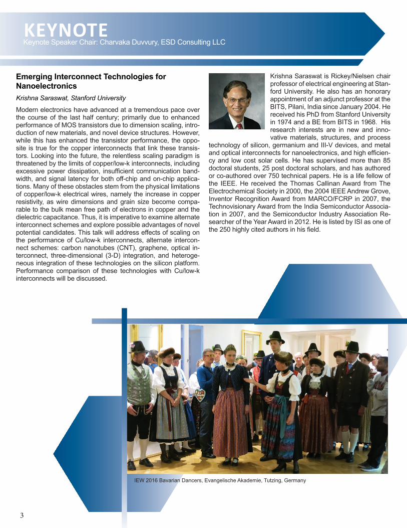
Emerging Interconnect Technologies for NanoelectronicsKrishna Saraswat, Stanford University
Modern electronics have advanced at a tremendous pace over the course of the last half century; primarily due to enhanced performance of MOS transistors due to dimension scaling, intro-duction of new materials, and novel device structures. However, while this has enhanced the transistor performance, the oppo-site is true for the copper interconnects that link these transis-tors. Looking into the future, the relentless scaling paradigm is threatened by the limits of copper/low-k interconnects, including excessive power dissipation, insufficient communication band-width, and signal latency for both off-chip and on-chip applica-tions. Many of these obstacles stem from the physical limitations of copper/low-k electrical wires, namely the increase in copper resistivity, as wire dimensions and grain size become compa-rable to the bulk mean free path of electrons in copper and the dielectric capacitance. Thus, it is imperative to examine alternate interconnect schemes and explore possible advantages of novel potential candidates. This talk will address effects of scaling on the performance of Cu/low-k interconnects, alternate intercon-nect schemes: carbon nanotubes (CNT), graphene, optical in-terconnect, three-dimensional (3-D) integration, and heteroge-neous integration of these technologies on the silicon platform. Performance comparison of these technologies with Cu/low-k interconnects will be discussed.
Krishna Saraswat is Rickey/Nielsen chair professor of electrical engineering at Stan-ford University. He also has an honorary appointment of an adjunct professor at the BITS, Pilani, India since January 2004. He received his PhD from Stanford University in 1974 and a BE from BITS in 1968. His research interests are in new and inno-vative materials, structures, and process
technology of silicon, germanium and III-V devices, and metal and optical interconnects for nanoelectronics, and high efficien-cy and low cost solar cells. He has supervised more than 85 doctoral students, 25 post doctoral scholars, and has authored or co-authored over 750 technical papers. He is a life fellow of the IEEE. He received the Thomas Callinan Award from The Electrochemical Society in 2000, the 2004 IEEE Andrew Grove, Inventor Recognition Award from MARCO/FCRP in 2007, the Technovisionary Award from the India Semiconductor Associa-tion in 2007, and the Semiconductor Industry Association Re-searcher of the Year Award in 2012. He is listed by ISI as one of the 250 highly cited authors in his field.
KEYNOTEKeynote Speaker Chair: Charvaka Duvvury, ESD Consulting LLC
3
IEW 2016 Bavarian Dancers, Evangelische Akademie, Tutzing, Germany

Invited Talk 1TBD
Invited Talk 2ESD Waveform CaptureElyse Rosenbaum, University of Illinois at Urbana-Champaign
Diagnosis of ESD failures requires familiarity with the ESD-induced current and voltage waveforms that appeared at the affected nodes in the circuit or system. Obtaining this information is difficult. Many nodes are not accessible to current or voltage probes and the inser-tion of a probe often changes the very waveform one is trying to measure. This presentation will review the challenges and proposed solutions for direct probing and it will describe various ESD voltage sensors that can be placed on-chip.
Elyse Rosenbaum is the Melvin and Anne Louise Hassebrock professor in electrical and computer engineering at the University of Illinois at Urbana-Champaign. She received a PhD in electrical engineering from University of California, Berkeley. She is currently the director of the NSF Center for Advanced Electronics through
Machine Learning, a joint project of the University of Illinois, Georgia Tech, and North Carolina State University. Her present research interests include component and system-level ESD reliability, transient latch-up, ESD-robust high-speed I/O circuit design, compact modeling of on-chip ESD protection devices, mitigation strategies for ESD-induced soft failures, and machine-learning aided behavioral modeling of microelectronic components and systems. Dr. Rosenbaum is currently an editor for IEEE Transactions on Electron Devices. She was the technical program chair for the 2016 International Reliability Physics Symposium. Dr. Rosenbaum is a fellow of the IEEE.
Invited Talk 3Cognitive Applications Platform: (Artificial) Intelligence at the EdgeJim Hogan, Vista Ventures, LLC
We sit at the cusp of an acceleration of human learning. The pace will increase dynamically in just a view years. The availabil-ity of unlimited compute power and storage in the cloud are here to enable this explosion of innovation.
According to IBM Chair and CEO Ginni Rometty, “think about digital business married with digital intelligence and you get cog-nitive,” Rometty said. “This is an era, cognitive era. It’s an era of technology. It’s an era of business for companies.”
Cognitive computing platforms have emerged and are becoming commercially available. Cognitive computing has been used to refer to new hardware and/or software that mimics the function-ing of the human brain and helps to improve human decision-making. Computing platforms, purpose-build applications to ad-dress specific behaviors resulting from, “systems that learn at scale, reason with purpose and interact with humans naturally.
In this talk let’s examine the data to see if it’s true. Then look at an abstracted view of the what it will take.
Jim Hogan is currently the managing partner of Vista Ventures, LLC. Jim has worked in the semiconductor design and manufacturing in-dustry for more than 40 years; gaining experi-ence as a senior executive and board director in electronic design automation, intellectual property, semiconductor equipment, material science, and IT companies. Jim was a gen-
eral partner at Telos Venture Partners and senior vice president of business development at Artisan Components Inc., now part of ARM Holdings PLC. He held executive engineering, market-ing, and operational management positions at Cadence Design Systems, Inc., National Semiconductor Corporation, and Phillips Semiconductor. Jim holds a BA in mathematics, a BS in com-puter science and an MBA; all from San Jose State University. He serves on several private companies’ board of directors. Ad-ditionally, Jim serves as a strategic advisor to several private and public companies.
INVITED TALKS
Invited Speaker Co-Chairs: Stephen Fairbanks, SRF Technologies, LLC Michael Khazhinsky, Silicon Laboratories, Inc.Invited talks are one of the key elements of the workshop, allowing attendees intimate exposure with industry leaders in focused areas of interest, as well as exposure to expertise outside our core fields. There are five invited talks this year where industry leaders and experts will share their thoughts on topics of keen interests to our engineering and scientific communities. Two of these talks from NXP and University of Illinois at Urbana-Champaign experts will be aligned with the main themes of this year’s workshop: ESD modeling and characterization, and on-die ESD measurements. We will also listen to an industry leading venture capitalist who will be discussing the latest trends in artificial intelligence and its impacts on our industries. Another invited talk from the University of California at Irvine will discuss the current market trends for IoT and their impacts on semiconductors.
4
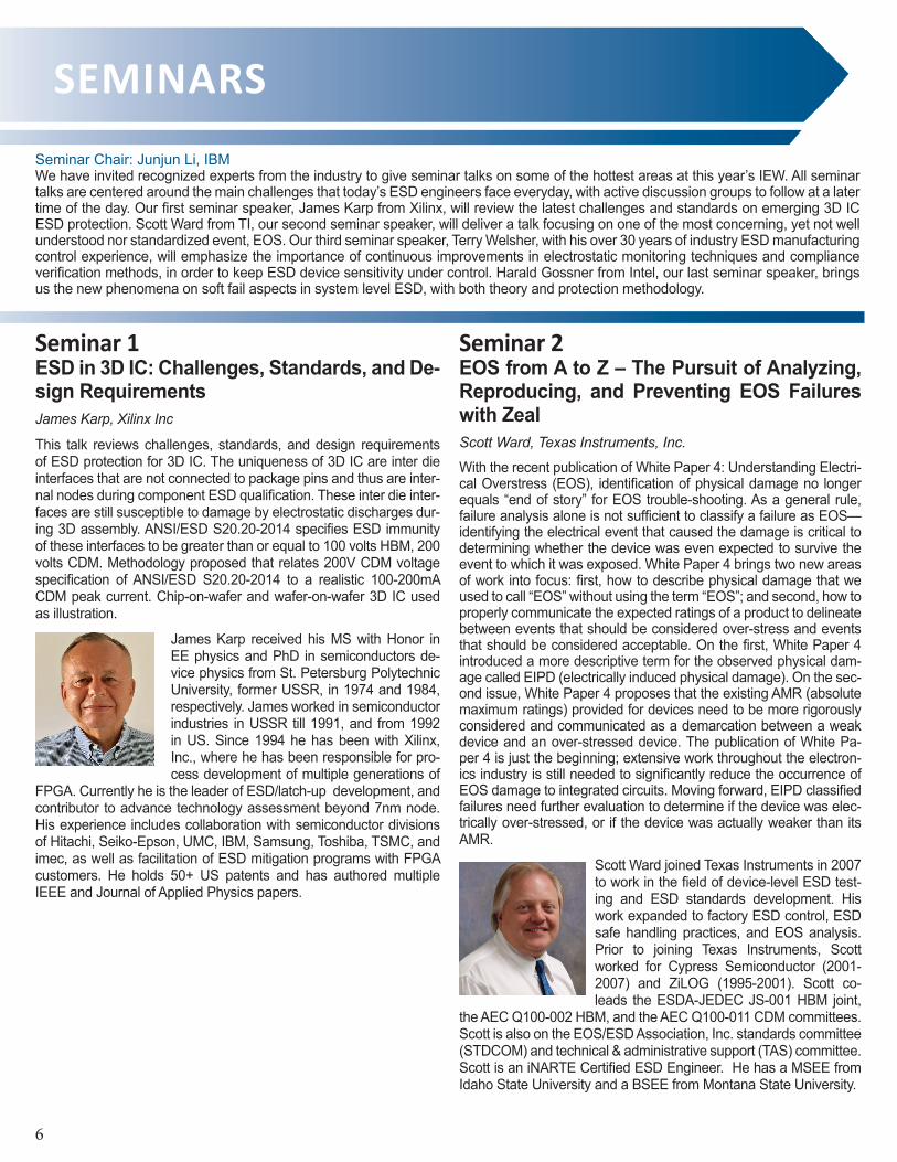
Invited Talk 5ESD Compact Models and their ApplicationsMichael “Michi” Stockinger, NXP Semiconductors
Compact models for ESD devices have become essential for ESD design as protection circuits have grown more complex and failure margins have narrowed. TLP device characteriza-tion data alone are not sufficient anymore - SPICE simulations are needed to accurately predict ESD performance. Standard models included in a physical design kit typically don’t capture the ESD operating regime. This talk will give a summary of pub-lished ESD models and their applications. The number of differ-ent modeling approaches and capabilities has become large as ESD models have been tailored to specific design constraints, methodologies, tool flows, and even personal preferences. This has called for a standardization of ESD compact models.
Michael “Michi” Stockinger received a MS and PhD in electrical engineering with highest hon-ors from Vienna University, Austria, in 1996 and 2000, respectively. His doctoral research focused on the optimization of ultra-low-power CMOS transistors. In 2000, he joined Motoro-la’s Semiconductor Products Sector in Austin, Texas; which became Freescale Semiconduc-
tor in 2004 and then NXP Semiconductors in 2016. Michael has been working in the field of ESD protection for advanced CMOS products since 2000. He is currently the technical leader of ESD design in NXP’s 32-bit microcontroller division. Michael’s on-chip ESD solutions have been implemented in the Qorivva, Kinetis, and ColdFire microcontroller product lines, to name a few. His latest research interests are in the field of on-chip protection so-lutions for system level (IEC) transient immunity. Michael was awarded the 2001 EOS/ESD Symposium Best Paper award, the 2003 EOS/ESD Symposium Best Paper and Best Presentation awards, and the 2013 EOS/ESD Symposium Best Paper and Outstanding Paper awards. He has authored and co-authored over 30 technical papers and teaches an ESDA tutorial. He has served in the TPC of several EOS/ESD Symposia and Interna-tional Reliability and Physics Symposia and as A/V co-chair of the International ESD Workshop (IEW). Michael holds 20 pat-ents on ESD design, with several others pending.
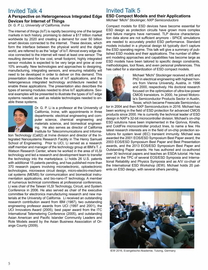
Invited Talk 4A Perspective on Heterogeneous Integrated Edge Devices for Internet of ThingsDr. G. P. Li, University of California, Irvine
The internet of things (IoT) is rapidly becoming one of the largest markets in tech history, promising to deliver a $17 trillion market worldwide by 2020 and creating a demand for over 50 billion smart devices connected to the internet. These devices, which form the interface between the physical world and the digital world, are referred to as the “edge” of IoT. Almost every edge de-vice connected to the internet will need at least one sensor. The resulting demand for low cost, small footprint, highly integrated sensor modules is expected to be very large and grow at over 10% annually. New technologies and approaches to designing, manufacturing, integrating sensors, and ensuring reliability will need to be developed in order to deliver on this demand. This presentation describes the nature of IoT applications, and the heterogeneous integrated technology architecture needed to enable these applications. The presentation also describes the types of sensing modules needed to drive IoT applications. Sev-eral examples will be presented to illustrate the types of IoT edge systems needed, as well as reliable technologies needed to en-able these systems.
Dr. G. P. Li is a professor at the University of California, Irvine, with appointments in three departments: electrical engineering and com-puter science, chemical engineering and materials science, and biomedical engineer-ing. He also serves as director of California Institute for Telecommunications and Informa-
tion Technology (Calit2) at Irvine division and director of the In-tegrated Nanosystems Research Facility in The Henry Samueli School of Engineering. Prior to UCI, Li served as a research staff member and manager of the technology group at IBM’s T. J. Watson Research Center, where he worked in the area of VLSI technology and led a research and development team to transfer the technology into the marketplace. Li holds 26 U.S. patents with additional 15 patents pending, and has published more than 370 research papers involving microelectronic, optoelectronic technologies, microwave circuit design, micro-electro-mechani-cal systems (MEMS) for communication and biomedical instru-mentation applications, and bio-nano-IT technology. A member of numerous technical committees at professional conferences, Li was chair of the Taiwan VLSI Technology, Circuit, and System Conference in 2006. He also served as chair of the executive committee for electronics manufacturing research and new ma-terials at the University of California. Li received an outstanding research contribution award from IBM (1987), two outstanding engineering professor awards from UCI (1997 and 2001), the UCI Innovators Award (2005), best paper award from the ITC International Telemetering Conference (2005), and outstanding Asian American and Pacific Islander Community Leaders and Role Models award by the Asian Business Association of Or-ange County (2009).
5
IEW 2016, Evangelische Akademie, Tutzing, Germany
SEMINARSSeminar Chair: Junjun Li, IBMWe have invited recognized experts from the industry to give seminar talks on some of the hottest areas at this year’s IEW. All seminar talks are centered around the main challenges that today’s ESD engineers face everyday, with active discussion groups to follow at a later time of the day. Our first seminar speaker, James Karp from Xilinx, will review the latest challenges and standards on emerging 3D IC ESD protection. Scott Ward from TI, our second seminar speaker, will deliver a talk focusing on one of the most concerning, yet not well understood nor standardized event, EOS. Our third seminar speaker, Terry Welsher, with his over 30 years of industry ESD manufacturing control experience, will emphasize the importance of continuous improvements in electrostatic monitoring techniques and compliance verification methods, in order to keep ESD device sensitivity under control. Harald Gossner from Intel, our last seminar speaker, brings us the new phenomena on soft fail aspects in system level ESD, with both theory and protection methodology.
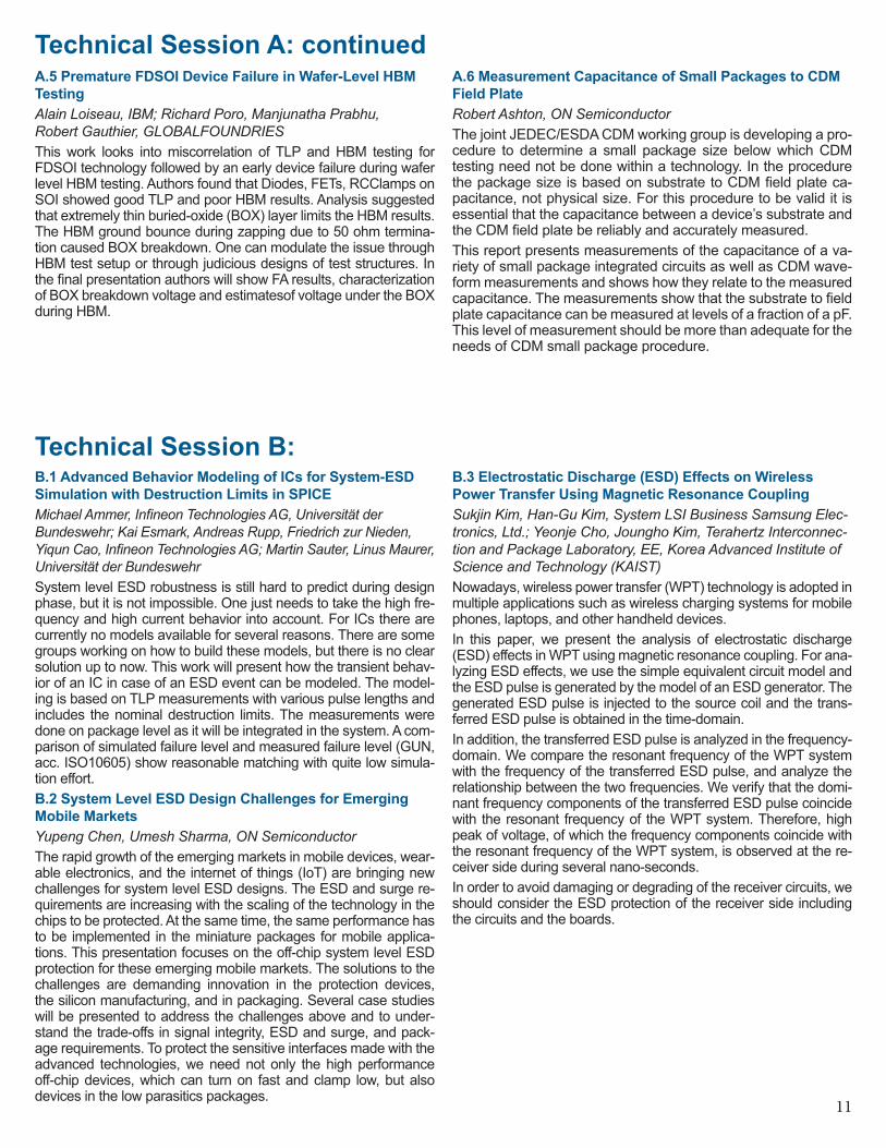
Seminar 1 ESD in 3D IC: Challenges, Standards, and De-sign RequirementsJames Karp, Xilinx Inc
This talk reviews challenges, standards, and design requirements of ESD protection for 3D IC. The uniqueness of 3D IC are inter die interfaces that are not connected to package pins and thus are inter-nal nodes during component ESD qualification. These inter die inter-faces are still susceptible to damage by electrostatic discharges dur-ing 3D assembly. ANSI/ESD S20.20-2014 specifies ESD immunity of these interfaces to be greater than or equal to 100 volts HBM, 200 volts CDM. Methodology proposed that relates 200V CDM voltage specification of ANSI/ESD S20.20-2014 to a realistic 100-200mA CDM peak current. Chip-on-wafer and wafer-on-wafer 3D IC used as illustration.
James Karp received his MS with Honor in EE physics and PhD in semiconductors de-vice physics from St. Petersburg Polytechnic University, former USSR, in 1974 and 1984, respectively. James worked in semiconductor industries in USSR till 1991, and from 1992 in US. Since 1994 he has been with Xilinx, Inc., where he has been responsible for pro-cess development of multiple generations of
FPGA. Currently he is the leader of ESD/latch-up development, and contributor to advance technology assessment beyond 7nm node. His experience includes collaboration with semiconductor divisions of Hitachi, Seiko-Epson, UMC, IBM, Samsung, Toshiba, TSMC, and imec, as well as facilitation of ESD mitigation programs with FPGA customers. He holds 50+ US patents and has authored multiple IEEE and Journal of Applied Physics papers.
Seminar 2 EOS from A to Z – The Pursuit of Analyzing, Reproducing, and Preventing EOS Failures with ZealScott Ward, Texas Instruments, Inc.
With the recent publication of White Paper 4: Understanding Electri-cal Overstress (EOS), identification of physical damage no longer equals “end of story” for EOS trouble-shooting. As a general rule, failure analysis alone is not sufficient to classify a failure as EOS—identifying the electrical event that caused the damage is critical to determining whether the device was even expected to survive the event to which it was exposed. White Paper 4 brings two new areas of work into focus: first, how to describe physical damage that we used to call “EOS” without using the term “EOS”; and second, how to properly communicate the expected ratings of a product to delineate between events that should be considered over-stress and events that should be considered acceptable. On the first, White Paper 4 introduced a more descriptive term for the observed physical dam-age called EIPD (electrically induced physical damage). On the sec-ond issue, White Paper 4 proposes that the existing AMR (absolute maximum ratings) provided for devices need to be more rigorously considered and communicated as a demarcation between a weak device and an over-stressed device. The publication of White Pa-per 4 is just the beginning; extensive work throughout the electron-ics industry is still needed to significantly reduce the occurrence of EOS damage to integrated circuits. Moving forward, EIPD classified failures need further evaluation to determine if the device was elec-trically over-stressed, or if the device was actually weaker than its AMR.
Scott Ward joined Texas Instruments in 2007 to work in the field of device-level ESD test-ing and ESD standards development. His work expanded to factory ESD control, ESD safe handling practices, and EOS analysis. Prior to joining Texas Instruments, Scott worked for Cypress Semiconductor (2001-2007) and ZiLOG (1995-2001). Scott co-leads the ESDA-JEDEC JS-001 HBM joint,
the AEC Q100-002 HBM, and the AEC Q100-011 CDM committees. Scott is also on the EOS/ESD Association, Inc. standards committee (STDCOM) and technical & administrative support (TAS) committee. Scott is an iNARTE Certified ESD Engineer. He has a MSEE from Idaho State University and a BSEE from Montana State University.
6

Seminar 4 Extending SEED Concept to Soft FailsHarald Gossner, Intel Corporation
System efficient ESD design (SEED) was proposed as design meth-odology for a matched PCB and IC protection concept in 2012 by In-dustry Council on ESD Target Levels. The base idea is to character-ize both TVS diode transient behavior and SoC IO behavior under high current conditions (e.g. by TLP,) to figure out the right match between on-chip and on-board protection for the given ESD stress waveform (e.g. IEC 61000-4-2). This is mostly addressing hard fails. Lately, investigations have shown that a triggering of soft fails can be provoked by injection of TLP pulses on a reference design board which cause similar soft failures as found in IEC testing of complete systems. This gives confidence that a TLP based characterization for soft fail thresholds on interfaces of IP blocks provides a valuable indicator for an improved, board and system design. The seminar provides an overview of the status of these investigations and an early assessment of the potential of this method.
Harald Gossner is senior principal engineer at Intel. He received his degree in physics (Dipl. Phys.) from the Ludwig-Maximilians-University, Munich in 1990 and his PhD in electrical engi-neering from the Universität der Bundeswehr, Munich in 1995. For 15 years he has worked on the development of ESD protection concepts with Siemens and Infineon Technologies. In
2010, he has joined Intel Mobile Communications overseeing the development of robust mobile systems.
Harald Gossner has authored and co-authored more than 100 tech-nical papers and two books in the field of ESD and device physics. He holds 50 patents on the same topic. He received the best pa-per award of EOS/ESD Symposium in 2005 and 2012. Regularly he is lecturing tutorials at ESREF, IRPS, and EOS/ESD symposia. He has served in technical program committees of IEDM, EOS/ESD Symposia and International ESD Workshop and is member of the board of directors of EOS/ESD Association, Inc. In 2006 he became cofounder and co-chair of the Industry Council on ESD Target Levels.
Seminar 3 ESD Control in Manufacturing: Techniques, Programs and ChallengesTerry Welsher, Dangelmayer Associates, LLC
Successful high-yield production and handling of ESD-sensitive de-vices has been the result of two mostly separate endeavors: 1. The development of electrostatic control methods and their implemen-tation into manufacturing processes; and 2. The design and fab-rication of special ESD protection circuits to improve device ESD robustness. The focus of the IEW has historically been on the latter. However, very few of the protection strategies in place today would be successful without a minimum level of ESD controls. In fact, it could be argued that without these controls Moore’s Law would have been stopped in its tracks. So, over the last several decades there has been a tenuous balance between control and protection which has not always been clear and has depended on target per-formance, manufacturing efficiency, and the evolution from primar-ily manual assembly to highly automated processes. In this semi-nar, we review the basic techniques for ESD control and how they have evolved with technology. We will discuss how they are merged into an overall program of ESD control, which includes monitoring techniques and compliance verification. We will also discuss how device-level ESD stress test methods have helped provide a practi-cal but imperfect link between ESD control and protection. Finally, we will present some case histories that exposed mismatches in the balance between control and protection and discuss challenges for future technologies.
Dr. Terry L. Welsher retired from Lucent Technol-ogies-Bell Laboratories Engineering Research Center in 2001, as the director of the quality, test, & reliability department. He began his career in Bell Labs in 1978; where he worked on electrical conduction mechanisms in insulating polymers and electrolytic corrosion failure mechanisms in electrical interconnection materials. In 1984, he
was appointed distinguished member of technical staff for his work in these fields. In 1986, he was promoted to technical manager to re-constitute the Bell Laboratories core expertise in electrostatic discharge (ESD). In 1994, he broadened his group’s activities to all aspects of hardware reliability for Lucent Technologies with special emphasis in environmental stress testing (EST) and product reliability prediction and planning. In 1997, he was promoted to director of the quality, test & reliability center of excellence where he directed the development and deployment of product quality, test and reliability assurance practices for Lucent Technologies business units. This work included design for testability of integrated circuits, board and system level test and diagnosis and special techniques for testing of RF and optoelectronic systems and components. After leaving Lu-cent, he became reliability director for LaserSharp Corporation, an optical fiber laser amplifier company, where he was responsible for product quality, reliability, and compliance. Since 2004, he has been senior vice president of Dangelmayer Associates, LLC, an EOS/ESD consulting firm. Dr. Welsher has been active in quality standards and road mapping activities with Sematech, EOS/ESD Association Inc., and the JEDEC 14 quality and reliability committee. He served on the board of directors of JEDEC 1999-2001. He is currently co-chair of the joint JEDEC/ESDA HBM and CDM ESD working groups, and member of the Board of Directors and Past President of the EOS/ESD Association. Recently, he has led the effort to harmonize and merge JEDEC and ESDA device testing standards. He holds a BS in chemistry from Florida State University and a PhD in chemical physics from the University of Texas at Austin. He is author or co-author of fifty papers in solid state physics, applied mathematics, organic chemistry, electronics reliability, and electrostatic discharge.
Demonstration at IEW 2016 poster session, Evangelische Akademie, Tutzing, Germany
7

Session A Parallel Groups-Monday 7:10-8:30 PMDG A.1 Inter Chip ESD design in 3D ICsModerator: Souvick Mitra, GLOBALFOUNDRIES, ([email protected])For chip to chip signaling in 3D IC’s it is highly desirable with re-spect to speed and power to use low voltage MOSFETs for the I/O’s. For the sake of area and loading, the ESD protection should be as small as possible. But how small? Whereas the package level tests and specs are well defined, 3D die assembly ESD tests are not defined at all. Nothing is known about the discharge wave-form. Should a ESDA/JEDEC committee be formed to develop a test methodology and corresponding spec?
DISCUSSION GROUPSDiscussion Groups Co-Chairs: Tom Meuse, Thermo Fisher ScientificEugene Worley, Qualcomm, Inc.The evening discussion groups are an integral part of the workshop. Two parallel discussion groups are offered each evening Monday through Wednesday. Each discussion group has one or more moderators with extensive expertise on the topic to help guide and inspire the discussion. The success of these sessions depends on your active participation. We encourage you to bring along data, ideas and other items of interest to share. Contacting session moderators with questions, comments, or suggestions prior to the event is also en-couraged. As the workshop approaches, please check the IEW web site for updates from the discussion group moderators. Interested in forming a new special interest group (SIGs), focused on one compelling topic of mutual interest? Please contact Tom Meuse and Gene Worley ([email protected], [email protected]) for SIG creation details.
Session BParallel Groups-Tuesday 7:10-8:30 PMDG B.1 Survival and Reliability Issues of the Auto Industry Moderator: TBDHow does the automotive industy deal with EOS? How does the industry prioritize EOS and reliability failures? What are the typi-cal failure modes and can anything be done to improve it? Are high temperature effects and high noise of the auto environment responsible for EOS failure? Do you design specifically for the auto industry or do you use a generic design and package and test to auto industry standards?
DG A.2 CDM TestingModerator: Tom Meuse, Thermo Fisher Scientific, ([email protected])With RF frequencies going up, faster SERDES ports, and extreme technology scaling, is it time to lower the CDM recommendation to 125 volts? Can factory ESD control equipment handle the job and at what cost? Also, what can be done to make low voltage dis-harges on CDM equipment less erratic? Contact methods are be-ing investigated as a way of improving the test method, will contact CDM help define new factory levels or set new standards?
DG B.2 IEC Testing Moderator: Hans Kunz, Texas Instruments, Inc. ([email protected])The IEC spec has issues as it relates to the real world and how to properly design a circuit for it. To begin with, contact discharge does not occur in the real world, but yet is specified for exposed metal surfaces. For air discharges, the initial spike is muted and, therefore, not much of a design issue but for contact discharge it can be. Is the HCP to ground plate capacitance 60 pF as found in one paper or 120 pF in another? Some advocate connecting the gun ground strap directly to the HCP for automotive applications. How are discharges introduced into connector signals where the connector has a robust ground shield? Likely direct pin discharges or through cables? Are HMM testers useful for design evaluation and where are they applied?
8

IEW 2016, Evangelische Akademie, Tutzing, Germany
Session C Parallel Groups-Wednesday 7:10-8:30 PMDG C.1 SEED Application to High Performance I/Os With and Without TVSModerators: Harald Gossner, Intel, ([email protected]); Jeff Dunnihoo, Pragma Design, ([email protected])As technology continues to downscale, SOC’s driving external ports and the lowering of the HBM spec (from 2 kV to 1 kV and even lower in the future) can translate into I/O’s where there are no TVS system level clamps that can protect them. Adding to the mix is the loading of TVS devices on high speed SERDES ports; not to mention the ambiguities of the IEC 61000-4-2 test. Whereas in the past, the I/O designer didn’t have to worry about interfacing to TVS clamps and passing an IEC spec, now he does. This session asks what does the desinger need to do to make sure his I/O’s can sucessfully interface to a TVS clamp to meet an IEC spec.
DG C.2 Absolute Maximum Rating (AMR)Moderator: Alan Righter, Analog Devices, ([email protected]) AMR is defined as the maximum voltage that may be applied to a device, beyond which damage (latent or otherwise) may occur according to JEDEC. Absent in the definition are temperature, cur-rent, failiure-In-time (FIT). Should there be a more precise difinition of AMR or leave it up to manufacturers to define the AMR of their products? Are there any industry specific definitions such as for the automobile industry?
DISCUSSION GROUPS continued
9
TECHNICAL SESSIONS
Technical Session Chair: Souvick Mitra, GLOBALFOUNDRIESThis year’s IEW technical program consists of two sessions, where peer-reviewed poster presentations are discussed together with the authors and interested colleagues. The authors will introduce their work in a short podium “teaser” presentation prior to the extended interactive discussion with the workshop participants at the poster sessions. This format allows an in-depth ex-change of ideas among a diverse audience, in a very informal setting. A wide variety of ESD subjects will be covered, including, system level ESD simulations and design techniques, ESD failure at wafer level testing, latch-up, TCAD, EOS, advanced FINFET circuit ESD design, and ideas for modeling and ESD testings.
Technical Session A: A.1 Skin-Depth Losses in Measurement Cables and Their Effect on CDM WaveformsTimothy J. Maloney, CAI
The ESDA/JEDEC JS-002 charged device model committee is considering standard practices for waveform measurement cables. Some degradation of signal strength is expected (de-pending on rise time), but to date there has been no quantita-tive estimate of impact with computed CDM waveforms with and without cable losses.Coaxial cable losses due to skin depth have long been studied, while more recently those losses at RF have been found to domi-nate over dielectric losses in most transmission lines, such as RG58C/U. A single time parameter, proportional to the square of cable length, fully describes a normalized impulse response for a given length of cable, with substantial accuracy. These are on record for many transmission lines and can be calculated from published cable loss data.For the first time, this work presents familiar CDM waveforms convolved with impulse response for cables of various lengths, thereby assessing the impact of skin depth. Around 8% lower Ipeak is seen for small objects for two meters of RG58C/U cable, 4% for one meter. This is still difficult to see in the presence of air spark variations. The CDM committee should converge on acceptable practice as it moves toward CCDM and more repro-ducible waveforms.A.2 Methodology to Enhance ESD Performance of Fully-Salicide 5 V MOSFET in Submicron CMOSKrishna Mohan Chavali, GLOBALFOUNDRIES5V MOSFETs are still used in almost all CMOS power-manage-ment integrated-circuits (PMICs) as power transistors. Conven-tional self-protection schemes (ballast resistor) and non-self pro-tection schemes (gate-coupling and substrate triggering) can’t be used for power transistors.A new scheme is proposed to enhance the ESD performances of 5V MOSFETs for power transistors. This scheme builds the backend resistors on top of the source and drain, without any increase in silicon footprint, unlike prior methods, while maintain-ing standard transistor IV performance.
A.3 TCAD Study on Electron Collection Efficiency during Latch-up TestYunfeng Xi, Michael G. Khazhinsky, Jeremy C. Smith Silicon LaboratoriesLatch-up is a significant reliability issue in semiconductor tech-nologies. Guard rings (GR) are widely used to protect against latch-up. Guard rings collect electrons and holes and prevent parasitic thyristor turn on. Many high-voltage applications use technologies with a low doped substrate to facilitate high voltage operation. In these technologies, carriers have longer lifetimes and larger diffusion lengths. Therefore, the efficient collection of free carriers is a key factor for improving latch-up immunity. This presentation studies two new configurations of guard rings in high voltage applications and compares guard ring collection efficiency to provide a latch-up free operating environment. Both configurations use guard rings built with high voltage N-well (HVNW) / N-buried layer (NBL). However, in the first configura-tion the guard ring is internal and connected to GND, while in the second configuration, an additional external guard ring is added and connected to VDD. TCAD simulation results of the electron current density and elec-tric field during latch-up test will be presented and discussed. The electron collection efficiency of these two guard ring con-figurations will be analyzed and compared. A.4 Update on JS-002: Component Results Compared to other Standards and Test Standards HarmonizationAlan Righter, Analog DevicesThis presentation will accomplish two objectives:It will present and discuss a significant amount of CDM compari-son result data (pass/fail level for at least 20 devices in a variety of packages/sizes) comparing JS-002 to JEDEC JESD22-C101, and possibly AEC Q-100, along with some failure comparison.It will also give an update on CDM standard harmonization ef-forts including AEC, IEC, and JEITA.
10
Technical Session B:
A.5 Premature FDSOI Device Failure in Wafer-Level HBM TestingAlain Loiseau, IBM; Richard Poro, Manjunatha Prabhu, Robert Gauthier, GLOBALFOUNDRIESThis work looks into miscorrelation of TLP and HBM testing for FDSOI technology followed by an early device failure during wafer level HBM testing. Authors found that Diodes, FETs, RCClamps on SOI showed good TLP and poor HBM results. Analysis suggested that extremely thin buried-oxide (BOX) layer limits the HBM results. The HBM ground bounce during zapping due to 50 ohm termina-tion caused BOX breakdown. One can modulate the issue through HBM test setup or through judicious designs of test structures. In the final presentation authors will show FA results, characterization of BOX breakdown voltage and estimatesof voltage under the BOX during HBM.
A.6 Measurement Capacitance of Small Packages to CDM Field PlateRobert Ashton, ON SemiconductorThe joint JEDEC/ESDA CDM working group is developing a pro-cedure to determine a small package size below which CDM testing need not be done within a technology. In the procedure the package size is based on substrate to CDM field plate ca-pacitance, not physical size. For this procedure to be valid it is essential that the capacitance between a device’s substrate and the CDM field plate be reliably and accurately measured.This report presents measurements of the capacitance of a va-riety of small package integrated circuits as well as CDM wave-form measurements and shows how they relate to the measured capacitance. The measurements show that the substrate to field plate capacitance can be measured at levels of a fraction of a pF. This level of measurement should be more than adequate for the needs of CDM small package procedure.
B.1 Advanced Behavior Modeling of ICs for System-ESD Simulation with Destruction Limits in SPICEMichael Ammer, Infineon Technologies AG, Universität der Bundeswehr; Kai Esmark, Andreas Rupp, Friedrich zur Nieden, Yiqun Cao, Infineon Technologies AG; Martin Sauter, Linus Maurer, Universität der BundeswehrSystem level ESD robustness is still hard to predict during design phase, but it is not impossible. One just needs to take the high fre-quency and high current behavior into account. For ICs there are currently no models available for several reasons. There are some groups working on how to build these models, but there is no clear solution up to now. This work will present how the transient behav-ior of an IC in case of an ESD event can be modeled. The model-ing is based on TLP measurements with various pulse lengths and includes the nominal destruction limits. The measurements were done on package level as it will be integrated in the system. A com-parison of simulated failure level and measured failure level (GUN, acc. ISO10605) show reasonable matching with quite low simula-tion effort.B.2 System Level ESD Design Challenges for Emerging Mobile MarketsYupeng Chen, Umesh Sharma, ON SemiconductorThe rapid growth of the emerging markets in mobile devices, wear-able electronics, and the internet of things (IoT) are bringing new challenges for system level ESD designs. The ESD and surge re-quirements are increasing with the scaling of the technology in the chips to be protected. At the same time, the same performance has to be implemented in the miniature packages for mobile applica-tions. This presentation focuses on the off-chip system level ESD protection for these emerging mobile markets. The solutions to the challenges are demanding innovation in the protection devices, the silicon manufacturing, and in packaging. Several case studies will be presented to address the challenges above and to under-stand the trade-offs in signal integrity, ESD and surge, and pack-age requirements. To protect the sensitive interfaces made with the advanced technologies, we need not only the high performance off-chip devices, which can turn on fast and clamp low, but also devices in the low parasitics packages.
Technical Session A: continued
B.3 Electrostatic Discharge (ESD) Effects on Wireless Power Transfer Using Magnetic Resonance CouplingSukjin Kim, Han-Gu Kim, System LSI Business Samsung Elec-tronics, Ltd.; Yeonje Cho, Joungho Kim, Terahertz Interconnec-tion and Package Laboratory, EE, Korea Advanced Institute of Science and Technology (KAIST)Nowadays, wireless power transfer (WPT) technology is adopted in multiple applications such as wireless charging systems for mobile phones, laptops, and other handheld devices. In this paper, we present the analysis of electrostatic discharge (ESD) effects in WPT using magnetic resonance coupling. For ana-lyzing ESD effects, we use the simple equivalent circuit model and the ESD pulse is generated by the model of an ESD generator. The generated ESD pulse is injected to the source coil and the trans-ferred ESD pulse is obtained in the time-domain. In addition, the transferred ESD pulse is analyzed in the frequency-domain. We compare the resonant frequency of the WPT system with the frequency of the transferred ESD pulse, and analyze the relationship between the two frequencies. We verify that the domi-nant frequency components of the transferred ESD pulse coincide with the resonant frequency of the WPT system. Therefore, high peak of voltage, of which the frequency components coincide with the resonant frequency of the WPT system, is observed at the re-ceiver side during several nano-seconds. In order to avoid damaging or degrading of the receiver circuits, we should consider the ESD protection of the receiver side including the circuits and the boards.
11

Technical Session B: continuedB.4 Device Compact Modeling for System Level ESD and EMC SimulationYuanzhong (Paul) Zhou, Analog DevicesCompliance with the IEC standards for system level ESD and EMC is imperative for semiconductor IC products to succeed in industrial and automotive markets. Using SPICE simula-tion enables this by reducing the number of silicon iterations required to pass the system level EMC/ESD tests and thus reduce time-to market.Such simulation requires a proper framework that includes models from individual devices within the IC, package parasit-ic, printed circuit board (PCB), test setup (e.g. IEC-61000-4-2), and ESD generators. In this presentation, a brief description on the framework is first presented. The focus is on compact modelling for on-board protection transient voltage suppres-sor (TVS) devices and on-chip protection SCR devices. The device models include not only quasi-static I-V characteristics measured by transmission line pulses (TLP) but also voltage overshoot in transient waveforms. The models also simulate current saturation effects in the SCR devices.The objective of the modeling is to achieve predictive system level simulations of failures. Failure models that can identify damage in the device due to thermal runaway or dielectric breakdown are also incorporated in the device. A SCR based model is used as failure detector for potential latch-up failures.
B.5 ESD Protection Circuit Design for 30 GHz HSS and Beyond in Advanced FinFETManjunatha Prabhu, Brian Hulse, Suresh C, Anand K, You Li, Robert G., GLOBALFOUNDRIESESD protection circuit design in advanced FinFET technology for high speed signalling (HSS) pins (>30 GHz) becomes ex-tremely challenging. To address this concern a systematic ap-proach to ESD design which makes best use of ESD design window and optimal use of simple ESD diodes is required. This work covers ESD design window and ESD protection scheme and feasibility analysis, capacitance calculations and comparison, HSS I/O TX/RX architectures and simulation and hardware results. Authors plan to show further capacitance optimization and ESD performance enhancement techniques in the final presentation.
B.6 Don‘t be “Strung“ Along by EOSDorothy Taylor, Texas InstrumentsObjective: To demonstrate that customer return’s root cause was concluded to be EOS, but evidence on subsequent re-turns indicates EOS conclusion was likely premature.Significance: Not looking beyond EOS evidence often results in missing the true root cause of the failure. First customer return - output transistor not operating cor-rectly.FA finds physical damage at output transistor– question aris-es: Is this EOS or ESD (subtleness of the damage brings in the ESD question)?Other returns from same customer and fab lot have same functional failure signature but absence of EOS. FA leads to discovery of TiW stringers causing failures. These stringers are in circuitry that drives the output transistor.Root-cause analysis of initial failing unit brings story into fo-cus: damage to output transistor could be due to stringer de-fect and not EOS/ESDStinger defect causes bias circuit to operate incorrectly.May have led to wrong bias on base of output transistor.Can no longer analyze this part for stringers: already de-pro-cessed.Key take-away: Without these additional failing units, first unit’s root cause would have been left as “EOS”. Physical damage alone cannot be used to determine EOS/ESD root-cause.
12

Sunday, May 7, 20171:30 PM-4:00 PM Registration: Pick up badges and handouts.
4:00 PM-4:30 PM Hotel check-in: Get room assignment & room key.
12:00 PM-1:30 PM Lunch1:30 PM-4:30 PM Free Time4:30 PM-6:00 PM Hosted Reception6:00 PM-7:30 PM Dinner7:30 PM-8:30 PM Welcome/Entertainment8:30 PM-9:30 PM Networking/Social Gathering
Monday, May 8, 20177:30 AM-9:00 AM Breakfast9:00 AM-9:30 AM Welcome 9:30 AM-10:40 AM Keynote: Emerging Interconnect Technologies for Nanoelectronics
Krishna Saraswat, Department of Electrical Engineering, Stanford University
10:40 AM-11:05 AM Break11:05 AM-12:05 PM Seminar 1: ESD in 3D IC: Challenges, Standards, and Design Requirements
James Karp, Xilinx Inc
12:05 PM-1:35 PM Lunch1:35 PM-2:35 PM Invited Talk 1: TBD
2:35 PM-3:20 PM Technical Session A: A.1 Skin-Depth Losses in Measurement Cables and Their Effect on CDM Waveforms Timothy J. Maloney, IntelA.2 Methodology to Enhance ESD Performance of Fullysalicide 5V MOSFET in Submicron CMOS Krishna Mohan Chavali, GLOBALFOUNDRIESA.3 TCAD Study on Electron Collection Efficiency during Latch-up Test Yunfeng Xi, Michael G. Khazhinsky, Jeremy C. Smith Silicon LaboratoriesA.4 Update on JS-002: Component Results Compared to other Standards and Test Standards Harmoni-zation Alan Righter, Analog DevicesA.5 Premature FDSOI Device Failure in Wafer-level HBM Testing Alain Loiseau, IBM; Richard Poro, Manjunatha Prabhu, Robert Gauthier, GLOBALFOUNDRIESA.6 Measurement Capacitance of Small Packages to CDM Field Plate Robert Ashton, ON Semiconductor
3:20 PM-4:35 PM Poster Discussion Session A4:35 PM-5:00 PM Break5:00 PM-6:00 PM Invited Talk 2: ESD Waveform Capture
Elyse Rosenbaum, University of Illinois at Urbana-Champaign
6:00 PM-7:10 PM Dinner7:10 PM-8:30 PM Discussion Group Session A: Parallel Groups
DG A.1 - Inter Chip ESD design in 3D ICsDG A.2 - CDM Testing
8:30 PM-9:30 PM Networking/Social Gathering
SCHEDULE
13

Tuesday, May 9, 20177:30 AM-9:00 AM Breakfast9:00 AM-9:10 AM Announcements9:10 AM-10:10 AM Invited Talk 3: Cognitive Applications Platform: (Artificial) Intelligence
at the Edge Jim Hogan, Vista Ventures, LLC
10:10 AM-10:20 AM Break10:20 AM-11:20 AM Invited Talk 4: A Perspective on Heterogeneous Integrated Edge Devices
for Internet of Things Dr. G. P. Li, University of California, Irvine
11:20 AM-12:00 PM Report on DG Sessions A12:00 PM-1:30 PM Lunch
1:30 PM-6:00 PM Open Time6:00 PM-7:10 PM Dinner7:10 PM-8:30 PM Discussion Group Session B: Parallel Groups
DG B.1 - Survival and Reliability Issues of the Auto IndustryDG B.2 - IEC Testing
8:30 PM-9:30 PM Networking/Social Gathering Wednesday, May 10, 2017
7:30 AM-9:00 AM Breakfast9:00 AM-9:10 AM Announcements9:10 AM-10:10 AM Seminar 2: EOS from A to Z – The Pursuit of Analyzing, Reproducing, and Pre-
venting EOS Failures with Zeal Scott Ward, Texas Instruments
10:10 AM-10:20 AM Break10:20 AM-11:20 AM Invited Talk 5: ESD Compact Models and their Applications
Michael “Michi” Stockinger, NXP Semiconductors
11:20 AM-12:00 PM Report on DG Sessions B12:00 PM-1:30 PM Lunch
1:30 PM-2:30 PM Seminar 3: ESD Control in Manufacturing: Techniques, Programs and ChallengesTerry Welsher, Dangelmayer Associates, LLC
2:30 PM-3:00 PM Picture / Break
3:00 PM-3:45 PM Technical Session B: B.1 Advanced Behavior Modeling of ICs for System-ESD Simulation with Destruction Limits in SPICE Michael Ammer, Infineon Technologies AG, Universität der Bundeswehr; Kai Esmark, Andreas Rupp, Friedrich zur Nieden, Yiqun Cao, Infineon Technologies AG; Martin Sauter, Linus Maurer, Universität der BundeswehrB.2 System Level ESD Design Challenges for Emerging Mobile Markets Yupeng Chen, Umesh Sharma, ON SemiconductorB.3 Electrostatic Discharge (ESD) Effects on Wireless Power Transfer Using Magnetic Resonance Cou-pling Sukjin Kim, Han-Gu Kim, System LSI Businessm Samsung Electronics, Ltd.; Yeonje Cho, Joungho Kim, Tera-hertz Interconnection and Package Laboratory, EE, Korea Advanced Institute of Science and Technology (KAIST)B.4 Device Compact Modeling for System Level ESD and EMC Simulation Yuanzhong (Paul) Zhou, Analog DevicesB.5 ESD Protection Circuit Design for 30GHz HSS and Beyond in Advanced FinFET Manjunatha Prabhu, Brian Hulse, Suresh C, Anand K, You Li, Robert G., GlobalfoundriesB.6 Don‘t be “Strung“ Along by EOS Dorothy Taylor, Texas Instruments
14
Wednesday, May 10, 2017 continued3:45 PM-5:00 PM Poster Discussion Session B5:00 PM-6:00 PM Seminar 4: Extending SEED Concept to Soft Fails
Harald Gossner, Intel Corporation
6:00 PM-7:10 PM Dinner7:10 PM-8:30 PM Discussion Group Session C: Parallel Groups
DG C.1 - SEED Application to High Performance I/Os With and Without TVS DG C.2 - Absolute Maximum Rating (AMR)
8:30 PM-9:30 PM Hosted ReceptionThursday, May 11, 2017
7:30 AM-9:00 AM Breakfast9:00 AM-9:10 AM Announcements9:10 AM-9:40 AM Industry Council Report9:40 AM-10:20 PM Report on DG Sessions C
10:20 AM-10:35 AM 2018 Announcements and ClosingBy 11:00 AM Hotel Check-Out
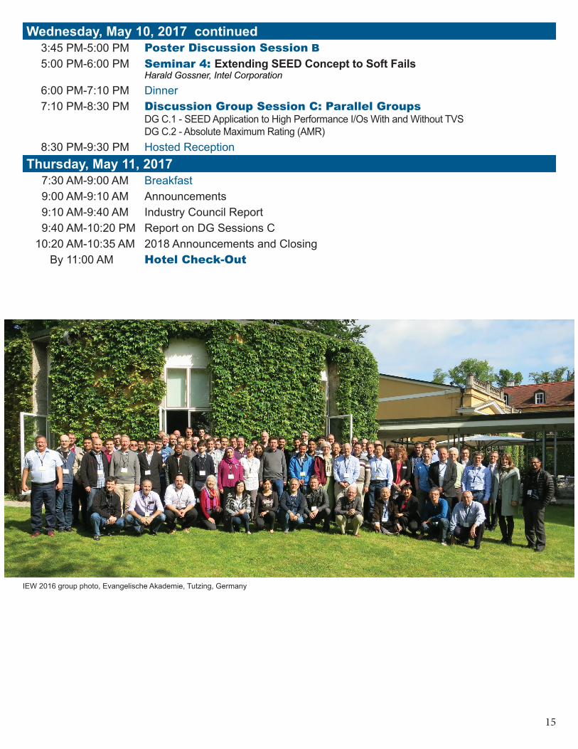
IEW 2016 group photo, Evangelische Akademie, Tutzing, Germany
15

Granlibakken Conference Center and Lodge, located in beautiful Tahoe City, provides an opportunity to meet in a relaxed, invigorating atmosphere. From the lodging to the activities, you’ll see that our multi-functional retreat conference center and resort has what it takes to be that perfect Lake Tahoe destination.
IEW ACCOMMODATIONS:At Granlibakken we have a wide variety of Lake Tahoe lodging options, from bedrooms, studios and suites to one to eight bedroom townhouses, each decorated to complement the resort’s natural Tahoe City setting.
Each room features the following amenities:• Cable television with DVD• Direct dial phone with voicemail and LAN / WLAN internet access• In-room coffee maker• In-room fan • Complimentary parking
All rooms come with our resort amenities which include an outdoor heated pool, outdoor hot tub, indoor sauna, hiking and biking trails, tennis courts and gym. On property Day Spa, Treetop Adventure Park, bike rentals and a ski & sledding hill are available for additional fees.
GUESTS AND SPOUSES:You are welcome to bring a guest to IEW. Accommodations are available for spouses and guests in the same room for an extra $300 US dollars per person. Guest fees are payable to ESDA. Guests will be charged for full stay, no partial stay allowed. Attendees must list guests with their initial registration to allow for room arrange-ments. For accommodations including children please contact ESDA for more information.
● Arrangements can be made for those with special dietary or physical requirements. Please send your require-ments with the registration or call 1-315-339-6937.
RESPONSIBILITIES OF ATTENDEES:Please come prepared to participate actively in the discussions and meetings by sharing your experiences, concerns, questions, views, technical information, and test data, as appropriate. Your active involvement in the formal, as well as in the informal meetings and activities, is the key ingredient for maximizing the value of the workshop for you and your fellow attendees. Enjoy IEW!
In keeping with the relaxed and informal atmosphere of the Workshop, we ask that attendees not overtly solicit, promote, or attempt to sell a commercial product or service at the Granlibakken Conference Center and Lodge. On the other hand, we strongly encourage making business acquaintances and arranging meetings to be held after the workshop.
ON-SITE GUEST ACTIVITIES: • Walking to Tahoe City or the Truckee River along our forest path (1.4 miles)• Playing a game of tennis on one of the resort’s five courts • Taking in the surrounding beauty on our private nature trail• Enjoying the sun beside our luxurious pool and hot tub area• Relaxing in our rejuvenating sauna• Building up a sweat on our outdoor par course• Hiking Tahoe’s Rim Trail, which borders the resort• Treetop ropes course and tours in our Adventure Park • Mountain bike rentals available on property, provided by West Shore Sports
TRAVEL ARRANGEMENTS & ACCOMMODATIONS
16
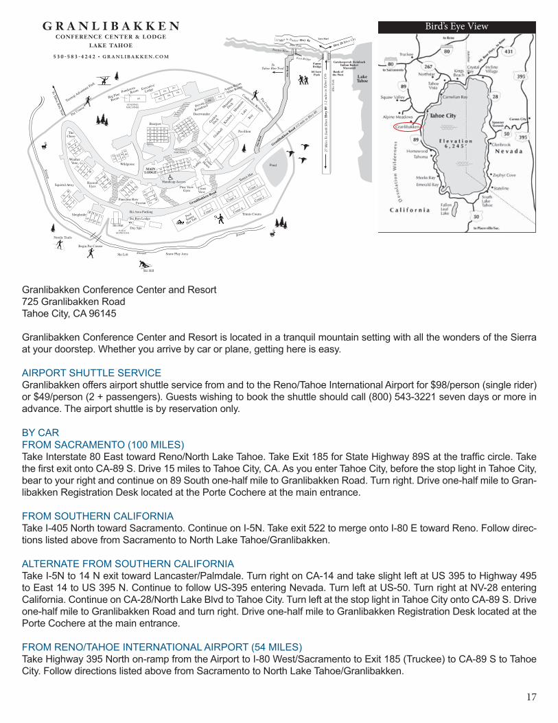
Granlibakken Conference Center and Resort725 Granlibakken RoadTahoe City, CA 96145
Granlibakken Conference Center and Resort is located in a tranquil mountain setting with all the wonders of the Sierra at your doorstep. Whether you arrive by car or plane, getting here is easy.
AIRPORT SHUTTLE SERVICEGranlibakken offers airport shuttle service from and to the Reno/Tahoe International Airport for $98/person (single rider) or $49/person (2 + passengers). Guests wishing to book the shuttle should call (800) 543-3221 seven days or more in advance. The airport shuttle is by reservation only.
BY CAR FROM SACRAMENTO (100 MILES)Take Interstate 80 East toward Reno/North Lake Tahoe. Take Exit 185 for State Highway 89S at the traffic circle. Take the first exit onto CA-89 S. Drive 15 miles to Tahoe City, CA. As you enter Tahoe City, before the stop light in Tahoe City, bear to your right and continue on 89 South one-half mile to Granlibakken Road. Turn right. Drive one-half mile to Gran-libakken Registration Desk located at the Porte Cochere at the main entrance.
FROM SOUTHERN CALIFORNIATake I-405 North toward Sacramento. Continue on I-5N. Take exit 522 to merge onto I-80 E toward Reno. Follow direc-tions listed above from Sacramento to North Lake Tahoe/Granlibakken.
ALTERNATE FROM SOUTHERN CALIFORNIATake I-5N to 14 N exit toward Lancaster/Palmdale. Turn right on CA-14 and take slight left at US 395 to Highway 495 to East 14 to US 395 N. Continue to follow US-395 entering Nevada. Turn left at US-50. Turn right at NV-28 entering California. Continue on CA-28/North Lake Blvd to Tahoe City. Turn left at the stop light in Tahoe City onto CA-89 S. Drive one-half mile to Granlibakken Road and turn right. Drive one-half mile to Granlibakken Registration Desk located at the Porte Cochere at the main entrance.
FROM RENO/TAHOE INTERNATIONAL AIRPORT (54 MILES)Take Highway 395 North on-ramp from the Airport to I-80 West/Sacramento to Exit 185 (Truckee) to CA-89 S to Tahoe City. Follow directions listed above from Sacramento to North Lake Tahoe/Granlibakken.
Pinecone Row
III
III
I
88
8786
85
IV I
IIII
7675
7473
Deerwander
Pavillion
CourtView
Par Course
Court 1
Court 2Court 3
Court 4Court 5
Pool
Sauna
Hot Tub
MAINLODGE
Foxrun
Snow Play Area
Ski Area Parking
Ski Lift
Ski Hut
Wildgoose
RacoonEyes
WeatherVane
Squirrel Away
Sleighride
Begin Par Course
Nordic Trails
Ski Hill
TheChase
Bearpaw 5153
5254
4547
4648
414237
34 3629 3128 3025 26
35
92IV
91 I
90II
89III
I
IIII
I
8079
7877
III II I84 83 82 81
II
IIIII
6162
6364
1514 12 11
2019 18
1724 2322
101
103
102
105
104
107
106
Granlibakken Road
5043
4440
3938333227
49
1016
21
Granha
ll
Lobby
Kitche
nM
ounta
inLak
eBay
CedarHouse
Tennis Courts
1 2
Pond
Stream
Stream
Par Course
Conference Rooms
Executive
Lodge
Big Pine
Room
Pine View Gym
Handicap Access Tennis Hut
Stream
II
110
Private
Residence
IVII
IIIIII
6867
6665
IIII
IIIII
7271
7069
Truckee River
ath
13 M
iles T
o So
uth
Sho r
e H
wy
89 1
. 2 m
iles t
o Ta
hoe
City
Bike
Pat
h
oTliarT miR eohaT
13 Miles to Truckee Hwy 89
Mounta
in
Deck
Garden
Deck
Foot Bridge
27 M
iles T
o So
u th
Shor
e H
wy
89 1
. 2 m
iles t
o Ta
hoe
City
Fire
Roa
d
Hwy 28 Tahoe CityAlbertson's
FannyBridge
Gatekeepers& SteinbachIndian Basket
MuseumS
LakeTahoe
Bank ofthe WestFi
re R
oad
64 Acre Park
Granlibakken Road 1/2 mile to Hwy 8
9
108
Ponderosa Room
VENDINGMACHINES
VENDINGMACHINES
Aspen Room
Alder Room
Bike P
To Tahoe Rim Trail
Treetop Adventure P
ark
Alumni
Day Spa
Ski Run Lodge WC
PUBLIC RESTROOMS
5 3 0 5 8 3 4 2 4 2 G R A N L I B A K K E N . C O M
Bird’s Eye View
17
Registration Fee $2,195Discount before March 24th: members $1,795 / non-members $1,995 The registration fee includes full workshop attendance and handout materials, four nights’ lodging (Sun-Wed), plus 12 meals (Sunday Lunch-Thursday Breakfast), as well as morning and afternoon breaks.
Workshop registration includes a room reservation and provided meals
Students wishing to apply for reduced registration Please contact EOS/ESD Association, Inc. prior to registering.
International ESD Workshop RegistrationMay 7-11, 2017 Granlibakken Conference Center & Lodge, Tahoe City, CA
Register Online at www.esda.org/events/iew/
Cancellation & refund requests will be considered if received in writing no later than March 24th 2017, and are subject to a $50 fee. Any other approved dispositions will also be assessed a $50 fee.
Register 5 or more people from one company at the same time and save $100 per personPlease contact EOS/ESD Association, Inc. prior to registering.
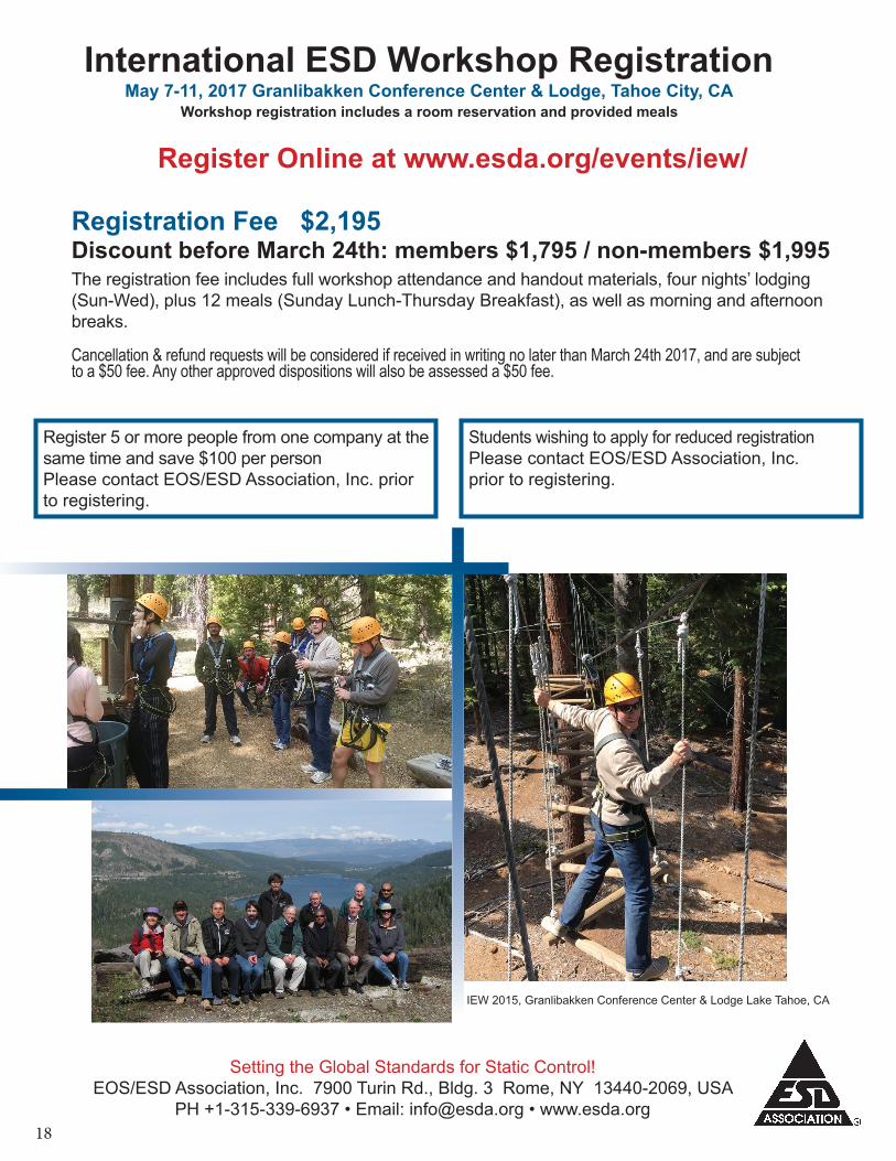
IEW 2015, Granlibakken Conference Center & Lodge Lake Tahoe, CA
Setting the Global Standards for Static Control! EOS/ESD Association, Inc. 7900 Turin Rd., Bldg. 3 Rome, NY 13440-2069, USA
PH +1-315-339-6937 • Email: [email protected] • www.esda.org18

Registration Fee $2,195Discount before March 24th: members $1,795 / non-members $1,995 The registration fee includes full workshop attendance and handout materials, four nights’ lodging (Sun-Wed), plus 12 meals (Sunday Lunch-Thursday Breakfast), as well as morning and afternoon snacks and drinks.
Method of Payment
Credit Card (check one) AMEX® Visa® MasterCard® Discover®
Card Number:
Exp. Date: Security Code:
Name on Card: Signature:
Billing Address:
Workshop registration includes a room reservation and provided meals
Attendee:
Company:
Address:
City: State: Zip: Country:
Phone: E-mail: Fax: Address is: (Please check one) home or office
Please check here if you would like a printed set of notes. Check if, under the Americans with Disabilities Act, you require any auxiliary aids or services.
Posters Will you be bringing a poster to the open poster session? Yes No If yes, what is the title of your poster?
Total Enclosed $ Make checks payable to: ESD Association
Purchase orders not accepted for registration
Check Only U.S. currency, checks drawn on a U.S. bank that is a member of the U.S. Federal Reserve will be accepted.
•Please indicate any special dietary needs.
Arrival: Date Time • Departure: Date Time
International ESD Workshop Registration FormMay 7-11, 2017 Granlibakken Conference Center & Lodge, Tahoe City, CA
Discussion Groups I am interested in the following discussion group(s)
Choose one from group A DG A.1 DG A.2
( ) ( )
•Please List Your Guests: Adults (Name) Guests staying in the room of a registered attendee will be charged $300 US dollars per person. Guest fees are payable to ESDA. Guests will be charged for full stay, no partial stay allowed. For accomodations including children please contact ESDA for more information.
Cancellation & refund requests will be considered if received in writing no later than March 24th 2017, and are subject to a $50 fee. Any other approved dispositions will also be assessed a $50 fee.
Choose one from group B DG B.1 DG B.2
Special Interest Groups Would you like to form a new SIG? Yes No If yes, what is the proposed topic for your group?
Choose one from group C DG C.1 DG C.2
Setting the Global Standards for Static Control! EOS/ESD Association, Inc. 7900 Turin Rd., Bldg. 3 Rome, NY 13440-2069, USA
PH +1-315-339-6937 • Email: [email protected] • www.esda.org
• Students wishing to apply for reduced registration please contact EOS/ESD Association, Inc. prior to registering. • Register 5 or more people from one company at the same time and save $100 per person. Please contact EOS/ESD Association, Inc. prior to registering.
19

International Electrostatic Discharge Workshop
Save the date:
IEW 2018
Setting the Global Standards for Static Control! EOS/ESD Association, Inc. 7900 Turin Rd., Bldg. 3 Rome, NY 13440-2069, USA
PH +1-315-339-6937 • Email: [email protected] • www.esda.org
May 14-18, 2018 2018 International
ESD Workshop (IEW)Priorij Corsendonk, Belgium
January 13, 2017 8:04 AM