(19) United States (12) Patent Application Publication … · (72) Inventor: Cheng-Yi Peng,...
70
US 20160211264A1 (19) United States (12) Patent Application Publication (10) Pub. No.: US 2016/0211264 A1 Peng (43) Pub. Date: Jul. 21, 2016 (54) INVERTERS AND MANUFACTURING HOIL 2L/84 (2006.01) METHODS THEREOF HOIL 29/06 (2006.01) HOIL 27/2 (2006.01) (71) Applicant: Taiwan Semiconductor Manufacturing (52) U.S. Cl. Company, Ltd., Hsin-Chu (TW) CPC ........ HOIL 27/0924 (2013.01); HOIL 29/0646 (2013.01); HOIL 27/1211 (2013.01); HOIL (72) Inventor: Cheng-Yi Peng, Hsin-Chu (TW) 21/845 (2013.01); HOIL 21/82.3821 (2013.01); (21) Appl. No.: 14/919,568 HOIL 21/823828 (2013.01) (22) Filed: Oct. 21, 2015 (57) ABSTRACT Related U.S. Application Data (63) Continuation-in-part of application No. 14/601,084, filed on Jan. 20, 2015. Inverters and methods of manufacture thereof are disclosed. s In some embodiments, an inverter includes a Substrate and a Publication Classification first tunnel FET (TFET) disposed over the substrate. The first TFET is a first fin field effect transistor (FinFET). A second (51) Int. Cl. TFET is over the first TFET. The Second TFET is a second HOIL 27/092 (2006.01) FinFET. A junction isolation region is disposed between a HOIL 2/8238 (2006.01) source of the first TFET and a source of the second TFET. 100 a
Transcript of (19) United States (12) Patent Application Publication … · (72) Inventor: Cheng-Yi Peng,...

US 20160211264A1
(19) United States (12) Patent Application Publication (10) Pub. No.: US 2016/0211264 A1
Peng (43) Pub. Date: Jul. 21, 2016
(54) INVERTERS AND MANUFACTURING HOIL 2L/84 (2006.01) METHODS THEREOF HOIL 29/06 (2006.01)
HOIL 27/2 (2006.01) (71) Applicant: Taiwan Semiconductor Manufacturing (52) U.S. Cl.
Company, Ltd., Hsin-Chu (TW) CPC ........ HOIL 27/0924 (2013.01); HOIL 29/0646 (2013.01); HOIL 27/1211 (2013.01); HOIL
(72) Inventor: Cheng-Yi Peng, Hsin-Chu (TW) 21/845 (2013.01); HOIL 21/82.3821 (2013.01); (21) Appl. No.: 14/919,568 HOIL 21/823828 (2013.01)
(22) Filed: Oct. 21, 2015 (57) ABSTRACT
Related U.S. Application Data (63) Continuation-in-part of application No. 14/601,084,
filed on Jan. 20, 2015. Inverters and methods of manufacture thereof are disclosed. s In some embodiments, an inverter includes a Substrate and a
Publication Classification first tunnel FET (TFET) disposed over the substrate. The first TFET is a first fin field effect transistor (FinFET). A second
(51) Int. Cl. TFET is over the first TFET. The Second TFET is a second HOIL 27/092 (2006.01) FinFET. A junction isolation region is disposed between a HOIL 2/8238 (2006.01) source of the first TFET and a source of the second TFET.
100 a

Patent Application Publication
100
Jul. 21, 2016 Sheet 1 of 51 US 2016/0211264 A1
104 sy
100 N--
t t t r r
--
100 Y
- H -- H -- H -- - - - - - - - - -
t + t t t t t t t t t t t t t t t t t t it - - - - - - - - - - - - - - - - - - - - -
H --

US 2016/0211264 A1 Jul. 21, 2016 Sheet 2 of 51 Patent Application Publication
00 N
a
Fig. 4
100
+ + --
a
Fig. 5

Patent Application Publication Jul. 21, 2016 Sheet 3 of 51 US 2016/0211264 A1
100 w 22
a ) 106/ gzz
114/1 16s. 4-106/114/116 -- 1-X
1/2w K1, t--- -
100 N-r,

US 2016/0211264 A1 Jul. 21, 2016 Sheet 4 of 51 Patent Application Publication
6 ‘???
~~~ ZOI 00I

US 2016/0211264 A1 Jul. 21, 2016 Sheet 5 of 51 Patent Application Publication
CI (~ |º 8ZI^---

US 2016/0211264 A1 Jul. 21, 2016 Sheet 6 of 51 Patent Application Publication
ZI ‘31-I CINO wgI T| J.HAN ||D PPA

US 2016/0211264 A1 Jul. 21, 2016 Sheet 7 of 51 Patent Application Publication
+ – – ++ + + + + +, ZI I++ , !—+ + +
39 || ~
} /* + + + |+ + + + +

Patent Application Publication Jul. 21, 2016 Sheet 8 of 51 US 2016/0211264 A1
100
00 N
130s

Patent Application Publication
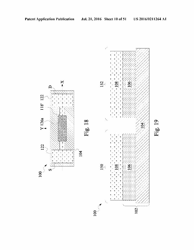
00 a
Jul. 21, 2016 Sheet 9 of 51 US 2016/0211264 A1
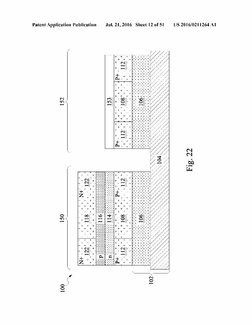
130 ---
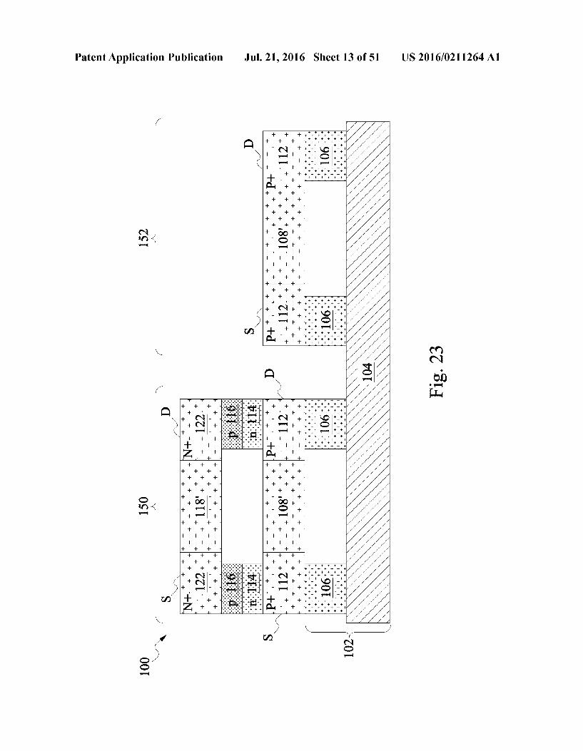
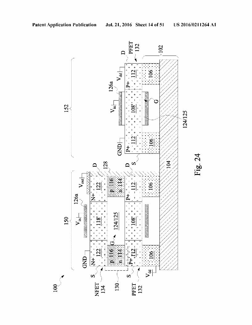
-- - - - - - - - - -- -- - - - - - - - - - -
-- - - -- + + + + -- - - - 108 -- - - - -
-- - - -- -- - - -- -- - - - - - - - - - -
124/125
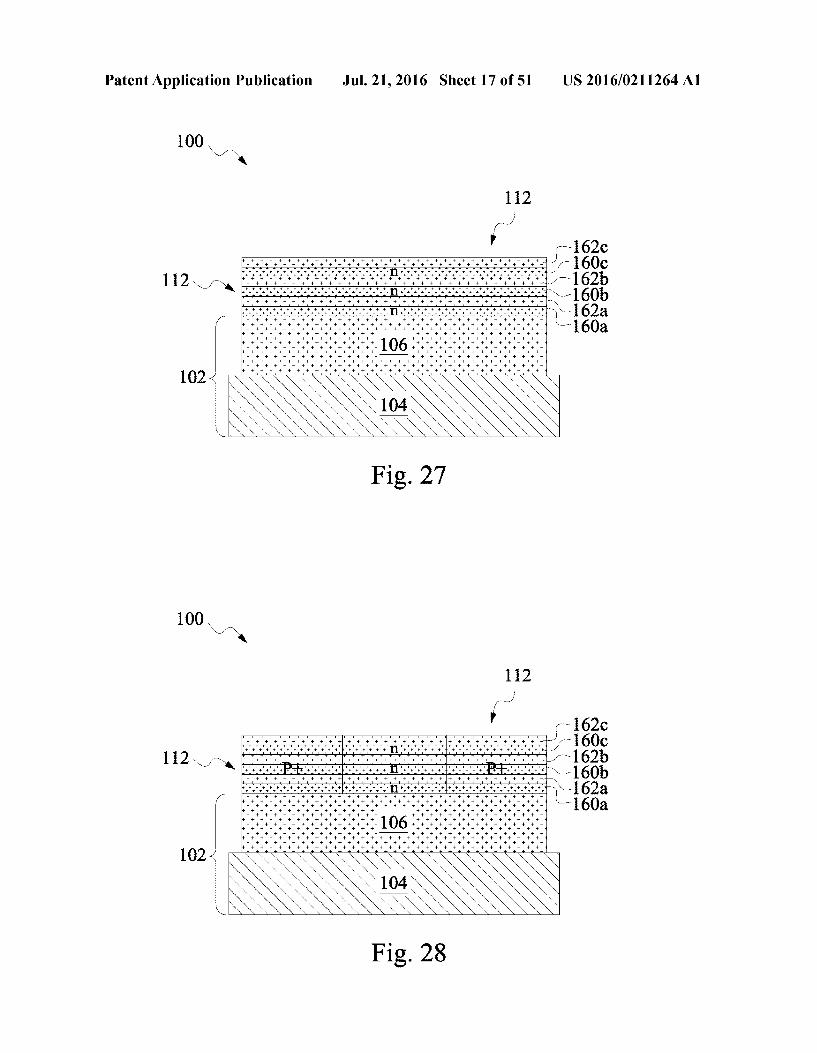
XX&
- - - - - - - - - -- -- -- - - --
t --- "t 108 ...P. - - - - - -- -- 1
-- - - - - - - --
24/125
----
US 2016/0211264 A1 Jul. 21, 2016 Sheet 10 of 51 Patent Application Publication
- - - - - - - H - - - - -
- - - - - - - -

US 2016/0211264 A1 Jul. 21, 2016 Sheet 11 of 51
+ + + + + + + + + + + + + + + + + + + + + +
+ + + + + + + + + + + + + + ++ + + + + + + + + + + + + + + + + + + + + + + -+ + + + + + + + + + + + + + + + + + + + + + + + + + + + + + + + + + + + + +
+ + + + + + + + + + + + + + + + + + + + + + + + + + + + + + + + + + + + + + + + + + + + + + + + + + + + + + + +
~)---------------------------------------------------------------—- ) --------------------------------------------------------------
Patent Application Publication
-- A
Patent Application Publication Jul. 21, 2016 Sheet 12 of 51 US 2016/0211264 A1
A.
-- --
-- --
en
H
--
---- i.
&
s S
US 2016/0211264 A1 Jul. 21, 2016 Sheet 13 of 51 Patent Application Publication
zši
+ + + + + + + + + + +
+ + +
+ + + +
+
+ + + + 801 ),
+ +
US 2016/0211264 A1 Jul. 21, 2016 Sheet 14 of 51 Patent Application Publication
ZOI <
xxxxxxxxxxxxxxxxxxxxxx §§
§§ SZI/VCI :) + + + + + + +
–||– + +
??-+ +- + ++ + +
+ +, ,8 ? I-+ +- + + + + + + + –||– + + + + + + H– §§

US 2016/0211264 A1 Jul. 21, 2016 Sheet 15 of 51 Patent Application Publication

US 2016/0211264 A1 Jul. 21, 2016 Sheet 16 of 51 Patent Application Publication
‘,º.***>) + ++ + + + + +}q–?—?)+ + + + + ++ + + + + + + ++ + + + + ++ + + ++ + + + + + ++ + + + + + + + ++ + + + + + ++ + + + ++ + + + + ++ + + + + + + ++ + + + + ++,+,+.*|\pp+ + + + + + ++ + + + + + + + ++ + + + + + ++ + + + ++ + + + + ++ + + + + +
+ ++ + + + + ++ + + ++ + + + + + ++ + + + + + + + ++ + + + + + ++ + + + ++ + + + + ++ + + + + +
+ ++ + + + + ++ + + ++ + + + + + ++ + + + + + + + ++ + + + + + ++ + + + ++ + + + + ++ + + + + +
+ ++ + + + + ++ + + ++ + + + + + ++ + + + + + + + ++ + + + + + ++ + + + ++ + + + + ++ + + + + +
+++ + + + ++ + ++ + + + +H- + + + + +
+ ++++ + + + + +„No.w!)+ , ' + d
+
&&&&&&&&&&&&
US 2016/0211264 A1 Jul. 21, 2016 Sheet 17 of 51 Patent Application Publication
N- a 100
160b N-62a
60a N--
t all
4th it deat it 4
all all.
kit -dd- 4 al al al
- - - - - - - - - - - - - - - - - - - - -
- - - - - - - - - - - - - - - - - - - - - - - - - - - - - - - - - - - - - --
- - - - - - - - - - - - - - - - - - - - -
ar
allis
- edit als
it the
als
is t-d
all - - - - - - - - - - - - - - - - - - - - -
- - - - - - - - - - - - - - - - - - - - - - - - - - - - - - - - - - -
- - - - - - - - - - - - - - - - - - - - -
- - - - - - - - - - - - - - - - - - - - - - - - - - - - - - - - - - - - - - - - - - at it it
Fig. 27
100
- - - - - - - -
- - - - - - - - - - - - -
-- - - - -
- - - - - - - - - - - -
- - - - - -
it -t EE -t-t-t-t-t-t-t-t-t-t- - F - F - F - F - F
- - - - - - - - - - - - - - - - 1.
- - - - - - - - - - - - - - - - - - -k-
- - - - - - - - - - - - -
E E - - - - - - - - - - - - - - - - - - - - - - - - - - - - - - - - -
r
.
- - - - - - - - - - - - - - - - - - - - -
T.T.T.T.T.T.T.T.T.T.T.T.T.T.T.T.T.T.T.T. -------------------- - - - - - - - - - - - - -
-- - - - - - - - - - - - - -
112 ra
Fig. 28

US 2016/0211264 A1 Jul. 21, 2016 Sheet 18 of 51 Patent Application Publication
164b -162e - 164a 162d
-164c 7-162f
100
Fig. 29
160c 162b
-160b Y-162a 160a
112 - a
Fig. 30

Patent Application Publication Jul. 21, 2016 Sheet 19 of 51 US 2016/0211264 A1
100 Ya 118'
wr-e-r-r-r------ wr-r- wr w-r-r- w-r-r--------
122 - - - - - - - - - - - - - - - - - - - - - - - - - - - - - - - - - -----
N/ - - - - - - - - - - - - - - - - - - - - - 1- 64b.
- - - - - - - - - - - - - - - - - - - st - - - - - - - - - -
- - - - - - - - - - - - - - - - - - - - - - - -

Patent Application
PEET-ul- 11 . . ." 32
Publication Jul. 21, 2016 Sheet 20 of 51
Exxxxx
US 2016/0211264 A1
+ + i + + + + i + + - - - - - - - - - - - -
- - - - - - - - - - - - - - - - - - - - -
- - - - - - - - - - .
A. 124/125 118' S - + , t t it
- - - - - - - - - - E - E - E - - -
+ + + + + + + + + i + -- - - - - - - - - - -
Vad:
108's ya —
W Y
- 162c
- 162b - 123 - 124
- 162a
---04

Patent Application Publication Jul. 21, 2016 Sheet 21 of 51 US 2016/0211264 A1
a 100'
- - - - - - - - - - - - - - Y
. . . . . . s: - - - - - - - - - - - - - - - - - - - - - - - - - - - - -
+ + i + + i + i + i + + + i + + + i + i + i + i + + i + i + + i + i + \----- - - - - - - - - - - - - - - - - - - - - - -
-- - - -- - - - - - - - - - - - - - - . . . . . . . . . . . . . . . . . . .
-- - - -- - - - - - - - - - - - - - - - - - - - - - - - - - - - - - -
... . . . . . . . . . . . . . . . . . . . . . . . . . . . . . . . . . . . . .
-- - - - - - - - - - - - - - - - - - - - -
100' 3:3-,-162f iii. - - - - - - - - - - - - - - - - - - - - - - - - - - - - - - - - --
r EE Y -1 64b N-162e
El El'EEEN it, t , , , , , , , , , , , , , , , , , , , , , , , , , , , , , , , , )
- - - - - - - - - - - - - - - - - - - - - - - - - - - - - - - - - - - - - +++++ +++++++++++++++++++++++++++++++++++++++++++ - v. . . . . . . . . . . . . . . . . . . . . . .- : - - - - - - - - - - - - - - - - - - - - - m -- - - - - - - - - - - - - - - ' ' ' ' ' ' ' ' ' ' ' ' ' -- - - - - - - - - - - - - - - -
- - - - - - - - - - - - - - - - + 4 + 3 + . - - - - - - -- - - - - - - - - - - - - - - -- - - - - - - - - - - - - - - -
- - - - - - - - - - - - - - - y it -- - - - - - - - - - - - - - - w - - - - - - - - - - - - - - -
- - - - - - - - - - - - - - - O W H - - - - - - - - - - - - - . . . . . . . . . . . . . . . - - - - - - - - - - - - - - - -- - - - - - - - - - - - - - - - - - - - - - - - - - - - - - - - - - - - - - - - - - - -
*.*.*.*.*.*.*.*.*.*.*.*.*.*.*.*.*.*.*.*.*.*.*.*.*.*.*.*.*.*.*.*.*.*.*.*.*.*.*.*.*.*.*.* - C - - - - - - - - - - - - - - - - - - - - - - - - - - - - - - - - - - - - - - - - - - - -
it is still it is + i + i + i + i + + i + i + i + i + F + i + i + i + i + i + i + i + i + + H+ i + i + i + + i + i + i + i + i + y - - - - - - - - - - - - - - - - - - - - - - - - - - - - - - - - - ^ C -- - - - - - - - - - - - - - - - - - - - - Y - - - - - - - - - - - - - - - - - - - - - - -
- - - - - - - - - - - - - - - - - - - - - + + + + + + i + + + + + + + + 4 + + + + +---1 F F --
N/S -- - - - -- - - - - - - - - - - - - - - - - - - - + + ------
A *.*.*.*.*.*.*.*.*.*.*.*.*.*.*.*.*.*.*.*.*.*.* +++++N - - - - - -- ..... - - - - - - - + 4 + · + - - - - - - - + 4 + - -->
- - - - -- - - - - - - - - -- - - - - - - - - ity
- - - - - - - - - - - - - - - - - - - - - Y-162a / - - - - - - - - - - - - - - - - - - - - - - - - - - - - - - - -
- - - - - - - - - - - - - - - - - - - - -
- - - - - - - - - - - - - - - - - - - - - - - - - - - - - - - - - - - - - - - - - - - - - - -
- - - - - - - - - - - - - - - - - - - - - - - - - - - - -
- - - - - - - - - - - - - - - - - - - - - - - - - - - - -
- - - - - - - - - - - - - -- - - - - - - - - - - - - - - - - - - -- - - - - - - - - - - - - -
l - - - - - - - - - - - - - - ld.

Patent Application Publication Jul. 21, 2016 Sheet 22 of 51 US 2016/0211264 A1
-- - - - - - - - - - - - - - - - - - - - - - - - - - - - - -
- - - - - - - - - - - - - - -
-- - - - - - - - - - - - - - - - - - - - S.
? iiitiitiitiitiitii,
-- - - - - - - - - - - - - - - ++++++++++++++ - - - - - - - - - - - - - - -- - - - - - - - - - - - - - - Y. -- - - - - - - - - - - - - - -- - - - - - - - - - - - - - - -- x
+ + + + + - - - - - - - - - , ... + + + + + + + + - - - - - - - 1 12" - - - - - - - - - - - - - - - - - - - - - - - - - - - - - --
... . . . . . . ... 1 +++++++++ + + + + + +/ 06: -- -- -- -- -- -- -- -- -- -- -- -- -- -- -- -- -- -- -- -- -- -- -- -- -- -- -- -- -- -- -- : -- :
100'
122's ra - - - - -
-- - - - - -
- 114 or 116' -:
::::::::::::::::::::::::::::::::::::::::::::::
- c.162b 12 Y- \a : :::::::::::::::::::::::::::::::::::::::::::: .*.*.*.*.*.*.*. *::::: -1 60 b
' ' ' ' '. ::::::::::::::::::::::::::::::::::::::::::::::::::::::::::::::::::::: *::::: - - - - - - - - - - - - - - F.
-- - - - - - -- - - -
106: 102 <

US 2016/0211264 A1 Jul. 21, 2016 Sheet 23 of 51 Patent Application Publication
89 '$1 {
EPPA
--?~~~~); *([-+ + + + + + + + + + + + + + + + + + + + + + + + + + + + + +
+
… + + + + + + + + + + + + + +
|(~~~~ 991 S
szi: ... --
- - -- - - -
- . it 4 + + i t t +
+ +
q| 8II SZI/VZI N` …+ + + + + + + + + + + + + + + + + + + + + + + + + + + + + +
H -

Patent Application Publication Jul. 21, 2016 Sheet 26 of 51 US 2016/0211264 A1

US 2016/0211264 A1
ZLH , !
Patent Application Publication
001

Patent Application Publication Jul. 21, 2016 Sheet 28 of 51 US 2016/0211264 A1
v x y v.
y < v
\ s y w
w
/ . A
A.

US 2016/0211264 A1 Jul. 21, 2016 Sheet 29 of 51 Patent Application Publication
St. NY -
y
99 I
O ^ 01. I • E

Patent Application Publication Jul. 21, 2016 Sheet 30 of 51 US 2016/0211264 A1
s 2

US 2016/0211264 A1 Jul. 21, 2016 Sheet 31 of 51 Patent Application Publication
OSV '31 I
.001
99 I

Patent Application Publication Jul. 21, 2016 Sheet 32 of 51 US 2016/0211264 A1

US 2016/0211264 A1 Jul. 21, 2016 Sheet 33 of 51 Patent Application Publication
vy, O ^ | OLI, ZLI~~
4 + -- - Y -
O r1"
100 I

Patent Application Publication Jul. 21, 2016 Sheet 34 of 51 US 2016/0211264 A1
5 s

Patent Application Publication Jul. 21, 2016 Sheet 35 of 51 US 2016/0211264 A1
g O< t
w w w w
) — / / / y N
A. C
-- YE +/ P vesse
NH NY + - O N vs.
Sp Y. - N -- + 7. t
H - + 7
\ 7
& / - - \d o \O C year
23 SS e - G - O - A ) \, \ \ \, \ w A ^ A A N
t i o \ . s
N r
O) a rea
t
-- Se - VC
y
t -
s

Patent Application Publication Jul. 21, 2016 Sheet 36 of 51 US 2016/0211264 A1
US 2016/0211264 A1 Jul. 21, 2016 Sheet 37 of 51 Patent Application Publication
.00I

Patent Application Publication Jul. 21, 2016 Sheet 38 of 51 US 2016/0211264 A1
s

US 2016/0211264 A1 Jul. 21, 2016 Sheet 39 of 51 Patent Application Publication
867 (318
„001

US 2016/0211264 A1 Jul. 21, 2016 Sheet 40 of 51 Patent Application Publication
LLI,

US 2016/0211264 A1 Jul. 21, 2016 Sheet 41 of 51 Patent Application Publication
809 ‘???

Patent Application Publication Jul. 21, 2016 Sheet 42 of 51 US 2016/0211264 A1

US 2016/0211264 A1 Jul. 21, 2016 Sheet 43 of 51 Patent Application Publication
ZOI

Patent Application Publication Jul. 21, 2016 Sheet 44 of 51 US 2016/0211264 A1
s
s
US 2016/0211264 A1 Jul. 21, 2016 Sheet 45 of 51 Patent Application Publication
Patent Application Publication Jul. 21, 2016 Sheet 46 of 51 US 2016/0211264 A1
s

US 2016/0211264 A1 Jul. 21, 2016 Sheet 47 of 51 Patent Application Publication
D99 318
ZOI
'99 I 001
v.
Patent Application Publication Jul. 21, 2016 Sheet 48 of 51 US 2016/0211264 A1
s

US 2016/0211264 A1 Jul. 21, 2016 Sheet 49 of 51 Patent Application Publication
ZOI*R}}

Patent Application Publication Jul. 21, 2016 Sheet 50 of 51 US 2016/0211264 A1
— - 126b S. E E E E E H = E E E E =
-/- P-+ + + + + + + - + + D 165'-'." 122'". ++" 18" ++ /
-- + -- + - + -- - - - - -- || -- - - - - --
- 124/125 1114 or 116 -- H - - - - - -
S. - - - - - - - - - - - -- -- - -- 1 D
163 YNN "... 108' ... Pt. 128 - a 1 12" + + - + i t + - + 1 12" + + Ya \- -- - - - - - - -- --
E. E. E. E. E. E. H. E. E. E. E. E. -- - - - - - -- - - - - --
-- - - - - - -- - - - - - --
106. 24/125 106. -- - - - - - -- - - - - --
-- - - - - - -- - - - - - -- S.
N - N N \, X -102
N N No4N
Fig. 55

Patent Application Publication Jul. 21, 2016 Sheet 51 of 51 US 2016/0211264 A1
1. 90 N-N
t 191 /
FORMA FIRST SEMICONDUCTIVE MATERIAL 08 OVER A SUBSTRATE O2
192 -----
FORMA SECOND SEMICONDUCTIVE MATERIAL 114 OR 116 OVER THE FIRST SEMCONDUCTIVE MATERAL 108
193 FORMATHIRD SEMICONDUCTIVE MATERIAL 18
OVER THE SECOND SEMICONDUCTIVE MATERAL 14 OR 16
194 IMPLANT A FIRST DOPANT COMPRISINGA FIRST DOPANT TYPE INTO THE FIRST SEMCONDUCTIVE MATERAL 108
TOFORMA DRAIN 112' (D) OF A FIRST TFET 163
195 IMPLANT A SECOND DOPANT COMPRISING ASECOND DOPANT
TYPE INTO THE FIRST SEMICONDUCTIVE MATERAL 108 TO FORMASOURCE 112' (S) OF THE FIRST TFET 163
196
IMPLANT THE FIRST DOPANT COMPRISING THE FIRST DOPANT TYPE INTO THE THIRD SEMICONDUCTIVE MATERAL 18
TO FORM A SOURCE 1 12" (S) OF A SECOND TFET 165
197 IMPLANT THE SECOND DOPANT COMPRISING THE SECOND DOPANT TYPE INTO THE THIRD SEMCONDUCTIVE MATERIAL
118 TOFORMA DRAIN 112' (D) OF THE SECOND TFET 165, WHEREIN THE FIRST TFET 163 AND THE SECOND TFET 165
COMPRISE FnBTS
Fig. 56

US 2016/0211264 A1
INVERTERS AND MANUFACTURING METHODS THEREOF
PRIORITY CLAIMAND CROSS-REFERENCE
0001. This application is a continuation-in-part of, and claims the benefit of U.S. patent application Ser. No. 14/601, 084 filed on Jan. 20, 2015 and entitled, "Semiconductor Devices and Manufacturing Methods Thereof.” which patent application is hereby incorporated herein by reference.
BACKGROUND
0002 Semiconductor devices are used in a variety of elec tronic applications, such as computers, cell phones, digital cameras, and other electronic equipment, as examples. Semi conductor devices are typically fabricated by sequentially depositing insulating or dielectric layers, conductive layers, and semiconductive layers of material over a semiconductor Substrate, and patterning the various material layers using lithography to form circuit components and elements thereon. 0003. A transistor is an element that is utilized extensively in semiconductor devices. There may be thousands of tran sistors on a single integrated circuit (IC) in some applications, for example. One common type of transistor used in semi conductor device fabrication is a metal oxide semiconductor field effect transistor (MOSFET). Two transistors may be coupled together to form an inverter. 0004 Multiple gate field-effect transistors (MuGFETs) are a recent development in semiconductor technology which typically are MOSFETs that incorporate more than one gate into a single device. The multiple gates may be controlled by a single gate electrode, where the multiple gate Surfaces act electrically as a single gate. The multiple gates may also be controlled by independent gate electrodes. One type of MuG FET is referred to as a fin field effect transistor (FinFET) device, which is a transistor structure with a fin-like semicon ductor channel that is raised vertically out of the silicon Surface of an integrated circuit.
BRIEF DESCRIPTION OF THE DRAWINGS
0005 Aspects of the present disclosure are best under stood from the following detailed description when read with the accompanying figures. It is noted that, in accordance with the standard practice in the industry, various features are not drawn to scale. In fact, the dimensions of the various features may be arbitrarily increased or reduced for clarity of discus S1O.
0006 FIGS. 1 through 11 are top views and cross-sec tional views that illustrate a method of manufacturing a semi conductor device at various stages in accordance with some embodiments of the present disclosure. 0007 FIG. 12 is a schematic of a semiconductor device in accordance with Some embodiments.
0008 FIG. 13 shows a cross-sectional view of a semicon ductor device in accordance with some embodiments.
0009 FIGS. 14 through 18 are cross-sectional views and a top view that illustrate a method of manufacturing a semicon ductor device at various stages in accordance with some embodiments.
0010 FIGS. 19 through 24 are cross-sectional views that illustrate a method of manufacturing a semiconductor device at various stages in accordance with some embodiments.
Jul. 21, 2016
0011 FIG.25 is a cross-sectional view of a semiconductor device in accordance with some embodiments. 0012 FIG. 26 is a cross-sectional view of a semiconductor device in accordance with some embodiments. (0013 FIGS. 27 through 33 are cross-sectional views that illustrate a semiconductor device at various stages of manu facturing in accordance with some embodiments. 0014 FIGS. 34 through 38 are cross-sectional views that illustrate an inverter at various stages of manufacturing in accordance with some embodiments of the present disclo SUC.
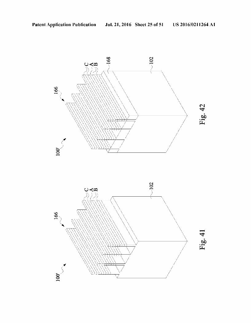
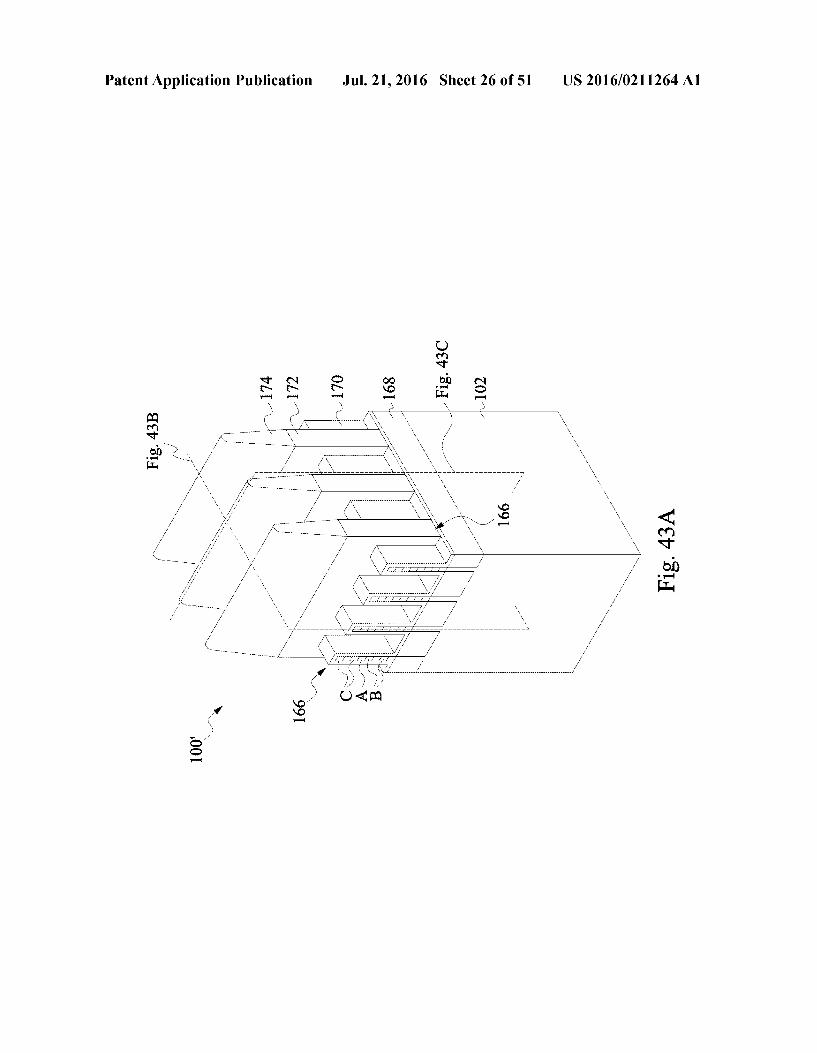
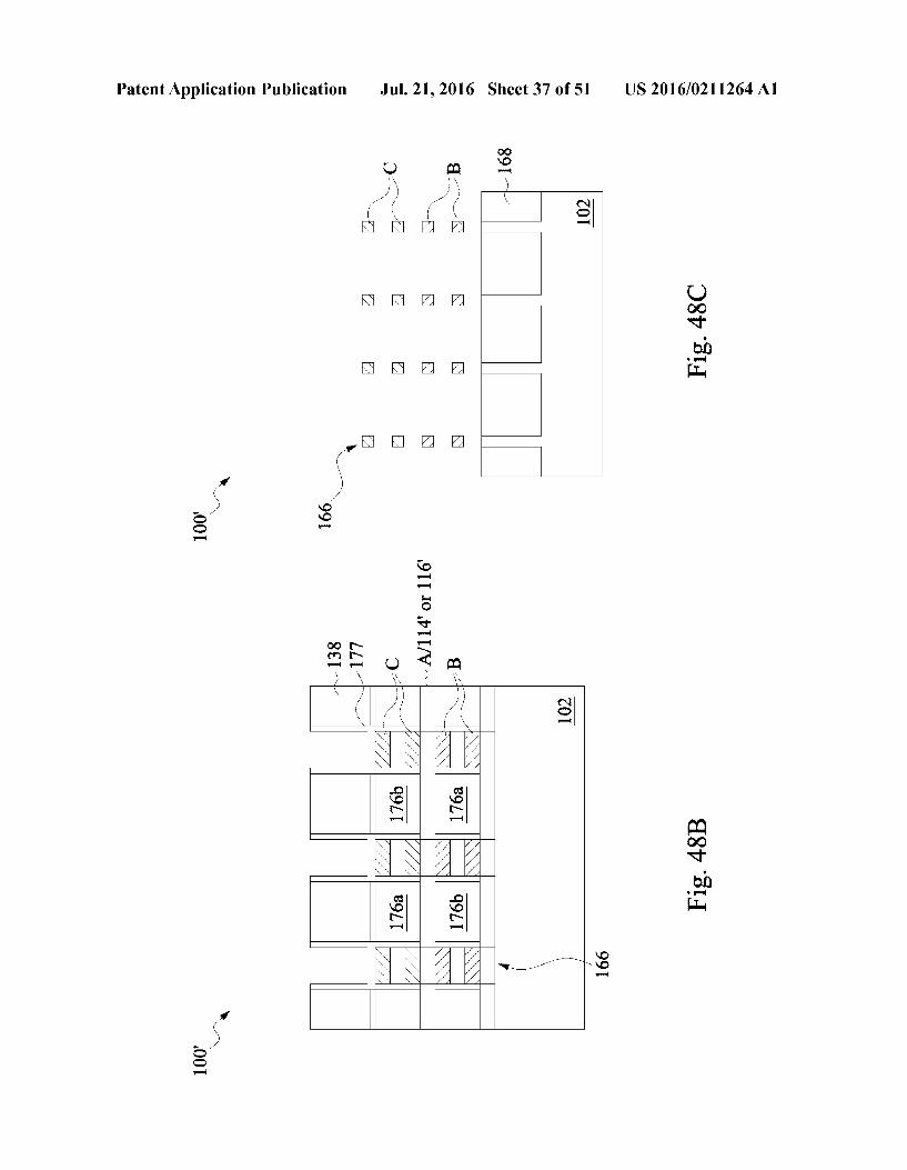
(0015 FIGS. 39 through 42, 43A through 43C, 44A through 44C, 45A through 45C, 46A through 46C, 47A through 47C, 48A through 48C, 49A through 49C, 50A through 50C, 51A through 51C, 52A through 52C, 53A through 53C, and 54A through 54Care perspective and cross sectional views that illustrate an inverter at various stages of manufacturing in accordance with some embodiments. 0016 FIG.55 shows a cross-sectional view of an inverter in accordance with some embodiments. 0017 FIG. 56 is a flow chart that illustrates a method of manufacturing an inverter in accordance with some embodi ments of the present disclosure.
DETAILED DESCRIPTION
0018. The following disclosure provides many different embodiments, or examples, for implementing different fea tures of the provided subject matter. Specific examples of components and arrangements are described below to sim plify the present disclosure. These are, of course, merely examples and are not intended to be limiting. For example, the formation of a first feature over or on a second feature in the description that follows may include embodiments in which the first and second features are formed in direct con tact, and may also include embodiments in which additional features may beformed between the first and second features, such that the first and second features may not be in direct contact. In addition, the present disclosure may repeat refer ence numerals and/or letters in the various examples. This repetition is for the purpose of simplicity and clarity and does not in itself dictate a relationship between the various embodiments and/or configurations discussed. 0019. Further, spatially relative terms, such as “beneath.” “below,” “lower,” “above,” “upper” and the like, may be used herein for ease of description to describe one element or feature's relationship to another element(s) or feature(s) as illustrated in the figures. The spatially relative terms are intended to encompass different orientations of the device in use or operation in addition to the orientation depicted in the figures. The apparatus may be otherwise oriented (rotated 90 degrees or at other orientations) and the spatially relative descriptors used herein may likewise be interpreted accord ingly. 0020 Semiconductor devices and methods of manufac ture thereof are disclosed in the present disclosure, wherein stacked FinFETs are formed that are coupled together and comprise inverters. A junction isolation material or region between sources of the FinFETs is self-aligned. Additional stacked or non-stacked FinFETs may also be formed during the various manufacturing steps and processes for the mate rial layers used to form the stacked FinFET inverters. The inverters comprise stacked NFETs and PFETs that may com prise single channels or multiple channels in Some embodi mentS.
US 2016/0211264 A1
0021. Some embodiments described herein are in refer ence to a specific context, namely forming fin field effect transistor (FinFET) devices. Aspects of this disclosure may also be applied in other contexts, such as forming other types of devices or semiconductor devices. Specific dimensions given below are for illustrative purposes for a given technol ogy node, Such as for about 15 nm technology or Smaller. Other embodiments contemplate different dimensions, par ticularly at different technology nodes. The figures discussed below are not necessarily drawn to Scale. 0022. Some embodiments described herein comprise two tunnel FETs (TFETs) comprising FinFETs that are coupled together to forman inverter. The TFETs may comprise single channels or multiple channels. The inverters comprise three dimensional (3D) stacked nanowire TFET inverters that have high mobility junction isolation in Some embodiments. 0023 FIGS. 1 through 11 are cross-sectional views and top views that illustrate a method of manufacturing a semi conductor device 100 comprising a three-dimensional (3D) stacked FinFET device at various stages of the manufacturing process in accordance with some embodiments of the present disclosure. In the illustrated embodiments, a stacked FinFET device is formed wherein a negative channel FET (NFET) 134 comprising a FinFET is stacked over a positive channel FET (PFET) 132 comprising a FinFET (see FIG. 10). The PFET 132 materials are first formed over a substrate 102, as shown in FIGS. 1 through 3, and the NFET 134 materials are then formed over the PFET 132 materials, as shown in FIGS. 4 and 5. The PFET 132 materials and NFET 134 materials are then patterned, as shown in FIGS. 6 through 8, and processing of the semiconductor device 100 is continued as shown in FIGS. 9 through 11 to form gate dielectrics, gates, and con tacts. In other embodiments, a stacked FinFET device may be formed wherein a PFET is stacked over an NFET.
0024. In the embodiments shown in FIGS. 1 through 11, a cyclic epitaxial growth and implantation process is used. Referring first to FIG.1, a top view of a semiconductor device 100 is shown. A cross-sectional view along anx plane of the semiconductor device 100 is shown in FIG.2. To manufacture the semiconductor device 100 in accordance with some embodiments, a substrate 102 is provided. The substrate 102 may be part of a wafer. The substrate 102 may comprise a semiconductor Substrate, such as a silicon Substrate, a silicon carbon Substrate, a silicon germanium Substrate, or a Sub strate formed of other semiconductor materials, as examples. The substrate 102 may comprise a bulk substrate, a semicon ductor-on-insulator (SOI) substrate, or other acceptable types of substrates. In some of the embodiments shown in FIGS. 1 and 2, the substrate 102 comprises an SOI substrate com prised of an insulating material 104 comprising an oxide Such as silicon dioxide, and a layer of semiconductive material 106 comprising silicon disposed on the insulating material 104. The insulating material 104 comprises a buried oxide (BOX) in some embodiments, for example. The semiconductive material 106 may be lightly doped with a p-type impurity. In the embodiments illustrated, the semiconductive material 106 is doped with a p-type impurity, such as B. Ga, or In to a concentration of about 1x10" cm to about 1x10 cm, as examples. The semiconductive material 106 may also be implanted using other materials to other concentration levels. In other embodiments, e.g., wherein a stacked FinFET device comprises a PFET stacked over an NFET, the semiconductive material 106 may be implanted with an n-type impurity. The insulating material 104 comprises a thickness of about 100
Jul. 21, 2016
um to about 500 um, or about 250 um to about 350 Lim, and the semiconductive material 106 comprises a thickness of about 20 nm to about 50 nm, or about 30 nm to about 40 nm, as examples. The substrate 102 may also comprise other mate rials and dimensions. A portion of the semiconductor device 100 is shown in the drawings of the present disclosure; the semiconductor device 100 may initially comprise a circular or other shapes in atop view in Some embodiments, for example. A plurality of PFETs, NFETs, and other devices is formed across a surface of the semiconductor device 100 in accor dance with some embodiments, for example. In other embodiments, the substrate 102 does not comprise an SOI substrate, and the portion of the semiconductor device 100 illustrated in the drawings is formed over shallow trench isolation (STI) regions, BOX regions, or other isolation regions of the Substrate 102, as another example. 0025. A first semiconductive material 108 is formed over the semiconductive material 106 of the substrate 102, as illustrated in FIG. 2 in the cross-sectional view. The first semiconductive material 108 is formed using an epitaxial growth process in some embodiments, for example. The first semiconductive material 108 may be formed using metal organic chemical vapor deposition (MOCVD), molecular beam epitaxy (MBE), liquid phase epitaxy (LPE), vapor phase epitaxy (VPE), selective epitaxial growth (SEG), the like, or a combination thereof. The first semiconductive mate rial 108 comprises SiGe. Ge. GeSn, SiGeSn, or a III-V mate rial in some embodiments, for example. In embodiments wherein the first semiconductive material 108 comprises a III-V material, the first semiconductive material 108 may comprise InAs, AlAs, GaAs, InP, GaN. InGaAs, InAlAs. GaSb, AlSb, AlP, or GaP, as examples. The first semiconduc tive material 108 comprises a thickness of about 3 nm to about 30 nm, or about 10 nm to about 20 nm in some embodiments, for example. The first semiconductive material 108 is in-situ doped with a desired doping level for channel regions of a PFET 132 in some embodiments, for example. The first semi conductive material 108 may also comprise other materials and dimensions, and may be formed using other methods. 0026. An implantation process is used to implant dopants into portions of the first semiconductive material 108 to form Source and drain regions 112 in the first semiconductive mate rial 108, as shown in FIG.3 in a cross-sectional view. A mask 110 is used in some embodiments to prevent the dopants from entering portions of the first semiconductive material 108, Such as channel regions disposed between the Source and drain regions 112. The mask 110 comprises a photoresist or other materials, which is deposited over the substrate 102 using a spin-on technique or other methods. The mask 110 is patterned using lithography, leaving the mask 110 shown in phantom (e.g., in dashed lines) in FIG. 3 disposed over regions of the first semiconductive material 108. The implan tation process is then performed for the first semiconductive material 108, forming source and drain regions 112 of a first FinFET device. The implanted dopants comprise p-type dopants in the embodiments illustrated. The p-type impurities may comprise B. Ga, or In implanted to a concentration of about 1x10 cm to about 5x10 cm, as examples. The implanted dopants may also comprise n-type dopants, e.g., in other embodiments wherein a stacked FinFET device com prises a PFET stacked over an NFET. The first semiconduc tive material 108 is doped in the source and drain regions 112 with a same type (i.e., n-type or p-type) of dopant that the semiconductive material 106 of the substrate 102 is doped

US 2016/0211264 A1
within some embodiments. The source and drain regions 112 may also be implanted using other materials to other concen tration levels. After the implantation process, the mask 110 may be removed using an acceptable ashing process and/oran etch process. The ashing process may include an oxygen containing plasma, for example. 0027. The source and drain regions 112 comprise a P+ material in Some embodiments, for example. The source and drain regions 112 comprise source (S) and drain (D) regions 112 of a PFET 132 (see FIG. 7), and other portions of the first semiconductive material 108 disposed between the source and drain regions 112 will be used to form channel regions of the PFET 132. The source and drain regions 112 may also comprise an N+ material, e.g., in other embodiments wherein a stacked FinFET device comprises a PFET stacked over an NFET. The first semiconductive material 108 comprises a different material thanamaterial of the semiconductive mate rial 106 of the substrate 102 in some embodiments, for example. 0028. A second semiconductive material 114 is formed over the first semiconductive material 108, as shown in FIG. 4 in a cross-sectional view. The second semiconductive mate rial 114 comprises silicon that is implanted with an n-type dopant in Some embodiments. The second semiconductive material 114 may also comprise silicon that is implanted with a p-type dopant, e.g., in other embodiments whereina Stacked FinFET device comprises a PFET stacked over an NFET. The second semiconductive material 114 is doped with a different type (i.e., n-type or p-type) of dopant than source and drain regions 112 within the first semiconductive material 108 are doped with in Some embodiments. The second semiconduc tive material 114 is epitaxially grown with in-situ doping included in the epitaxial growth process in some embodi ments, for example. The second semiconductive material 114 is doped an n-type dopant Such as P, AS, or Sb to a concen tration of about 1x10" cm to about 1x10 cm, as examples. The second semiconductive material 114 com prises a thickness of about 10 nm to about 30 nm, or about 15 nm to about 25 nm. The second semiconductive material 114 may also comprise other materials, dimensions, dopants, dopant concentration levels, and formation methods. As other examples, the second semiconductive material 114 may be epitaxially grown or deposited, and an implantation process may be used to dope the second semiconductive material 114. 0029. A third semiconductive material 116 is formed over the second semiconductive material 114, also shown in FIG. 4. The third semiconductive material 116 comprises silicon that is implanted with a p-type dopant in Some embodiments. The third semiconductive material 116 may also comprise silicon that is implanted with an n-type dopant, e.g., in other embodiments wherein a stacked FinFET device comprises a PFET stacked overan NFET. The third semiconductive mate rial 116 is doped with a different type (i.e., n-type or p-type) of dopant than the second semiconductive material 114 is doped with in some embodiments. The third semiconductive material 116 is epitaxially grown within-situ doping included in the epitaxial growth process, for example. The third semi conductive material 116 is doped with a p-type dopant Such as B. Ga, or Into a concentration of about 1x10" cm to about 1x10" cm, as examples. The third semiconductive material 116 comprises a thickness of about 10 nm to about 30 nm, or about 15 nm to about 25 nm. The third semiconductive mate rial 116 may also comprise other materials, dimensions, dopants, dopant concentration levels, and formation methods.
Jul. 21, 2016
As other examples, the third semiconductive material 116 may be epitaxially grown or deposited, and an implantation process may be used to dope the third semiconductive mate rial 116.
0030 The second semiconductive material 114 and the third semiconductive material 116 are later patterned to form a junction isolation material 130 (see FIG.7) in some embodi ments that is advantageously self-aligned, to be described further herein.
0031. A fourth semiconductive material 118 is then formed over the third semiconductive material 116 using an epitaxial growth process, as illustrated in FIG. 5 in a cross sectional view. As deposited, the fourth semiconductive material 118 comprises similar materials and dimensions as described for the first semiconductive material 108. The fourth semiconductive material 118 is in-situ doped with a desired doping level for channel regions of an NFET 134 in Some embodiments, for example. A mask 120 (shown in phantom in FIG. 5) similar to the mask 110 used to implant dopants into source and drain regions 112 formed within the first semiconductive material 108 is deposited over the fourth semiconductive material 118. An implantation process is then used to implant dopants into the fourth semiconductive mate rial 118 and form source and drain regions 122 in the fourth semiconductive material 118. The dopants implanted into the fourth semiconductive material 118 comprise a different type (i.e. p-type or n-type) than the dopants implanted into the first semiconductive material 108.
0032. The fourth semiconductive material 118 is implanted with an n-type dopant in Some embodiments to form the source and drain regions 122. The fourth semicon ductive material 118 may also be implanted with a p-type dopant, e.g., in other embodiments wherein a stacked FinFET device comprises a PFET stacked over an NFET. The fourth semiconductive material 118 is doped with a different type (i.e., n-type or p-type) of dopant than the Source and drain regions 112 within the first semiconductive material 108 are doped with in some embodiments. The fourth semiconduc tive material 118 is also doped with a different type (i.e., n-type or p-type) of dopant than the third semiconductive material 116 is doped with in some embodiments. The fourth semiconductive material 114 is doped with an n-type dopant such as P. As, or Sb to a concentration of about 1x10 cm to about 1x10 cm, as examples. The fourth semiconduc tive material 118 may also be implanted with other dopants in other dopant concentration levels. 0033. The source and drain regions 122 comprise an N+ material in Some embodiments, for example. The source and drain regions 122 comprise source (S) and drain (D) regions 122 of an NFET 134 (see FIG. 10), and other portions of the fourth semiconductive material 118 disposed between the source and drain regions 122 will be used to form channel regions of the NFET 134. The source and drain regions 122 may also comprise a P+ material, e.g., in other embodiments wherein a stacked FinFET device comprises a PFET stacked overan NFET. After the implantation process used to dope the fourth semiconductive material 118 to form the source and drain regions 122, the mask 120 is removed using an ashing process and/or etch process. 0034. After the implantation process used to dope the fourth semiconductive material 118 to form the source and drain regions 122, and/or after the implantation process used to dope the first semiconductive material 108 to form the Source and drain regions 112, the implanted dopants are then

US 2016/0211264 A1
activated, e.g., by heating the semiconductor device 100 to a predetermined temperature for a predetermined period of time. 0035. The semiconductor device 100 is then patterned using lithography to form channel regions 108' and 118' com prised of the first semiconductive material 108 and the fourth semiconductive material 118, respectively, as illustrated in a top view in FIG. 6, a cross-sectional x plane view in FIG. 7, and a cross-sectional y plane view in FIG.8. Portions of the first semiconductive material 108 after the patterning process comprise channel regions 108', and portions of the second semiconductive material 118 after the patterning process comprise channel regions 118'. The source and drain regions 112 and 122 are also defined during the patterning process for the channel regions 108' and 118'. The shapes of the source (S) and drain (D) regions 112 and 122 are defined in the patterning process, for example. 0036. A masking material such as a photoresist, not shown, is deposited over the fourth semiconductive material 118, and the masking material is patterned with a desired shape of channel regions 108' and 118 and source (S) and drain (D) regions 112 and 122 of the PFET 132 and the NFET 134 (see FIG. 10), respectively. The patterning process is performed using a Suitable etch process, such as a reactive ion etch (RIE), a neutral beam etch (NBE), tetramethyalammo nium hydroxide (TMAH), ammonium hydroxide (NHOH), a wet etchant capable of etching silicon with good etch selec tivity between silicon and a material of the insulating material 104, the like, or a combination thereof, using the masking material as an etch mask. The etch process may be anisotropic or isotropic and may comprise a selective etch process, as examples. The etch process used to form the channel regions 108' and 118'' and source (S) and drain (D) regions 112 and 122 of the PFET 132 and the NFET 134 may also comprise other types of etch processes and properties. The masking material is then removed using anashing process and/or etch process. 0037. A width of the channel regions 108' and 118' com prise a dimension W, wherein dimension W comprises about 5 nm to about 50, or about 10 nm to about 30 nm in some embodiments, as shown in the top view in FIG. 6. A thickness of the channel regions 108' and 118' comprise a dimension T (see FIG. 7), wherein dimension T comprises a thickness of the first semiconductive material 108 and the fourth semicon ductive material 118. Dimension T comprises about 3 nm to about 30 nm, or about 10 nm to about 20 nm in some embodi ments, for example. Dimensions W and T may also comprise other values. Channel region 108" is disposed beneath channel region 118', as illustrated in the X plane view in FIG. 7 and in they plane view in FIG.8. The channel regions 108' and 118' may comprise Substantially square or rectangular shapes in the cross-sectionally plane view shown in FIG.8. The channel regions 108' and 118 may also comprise substantially square or rectangular shapes with rounded corners, as a result of the etch process used to pattern the first and fourth semiconduc tive materials 108 and 118. 0038. The channel regions 108' and 118' comprise single channels in the embodiments shown in FIG. 1 through 10. Either one of the channel regions 108' and 108', or both, may comprise multiple channels formed in the horizontal direc tion (see FIG. 11) or in the vertical direction (see FIGS.32 and 33). 0039. The semiconductive material 106 of the substrate 102, the second semiconductive material 114, and the third
Jul. 21, 2016
semiconductive material 116 etch at a faster rate than the first and fourth semiconductive materials 108 and 118 during the etch process in some embodiments, so that the semiconduc tive material 106, the second semiconductive material 114, and the third semiconductive material 116 comprise an under cut beneath and/or above the first and fourth semiconductive materials 108 and 118, as illustrated in FIGS. 6 and 7. A selective etch process may be used that forms a predeter mined amount of undercut beneath and above the source (S) and drain (D) regions 112 and 122. The amount of the under cut comprises about /2 of dimension W, or about (/2*W) in Some embodiments. The amount of the undercut may also comprise other values and relative values to the width of the channel regions 108' and 118' comprising dimension W. The undercut may be formed on one or more sides of the semi conductive material 106, the second semiconductive material 114, and the third semiconductive material 116. 0040. A gate dielectric 123 and a gate material 124/125 are formed around each of the channel regions 108' and 118', and contacts 126a that are coupled to the gates (G) 124/125 and contacts 126b that are coupled to drain (D) regions 112 and 122 of the PFET 132 and the NFET 134 are formed, as shown in FIG. 9 in a top view, in FIG. 10 in a cross-sectional x plane view, and in FIG. 11 in a cross-sectional y plane view of the semiconductor device 100. The gate dielectrics 123 and gates 124/125 comprise a gate all around (GAA) structure around the channel regions 108' and 118' in some embodiments, for example. 0041. The gate dielectrics 123 may comprise SiO, Al2O, ZrO, Hf), TiO, or a combination or multiple layers thereof, as examples. The gate dielectrics 123 may comprise a material having a dielectric constant or k value of greater than a dielectric constant of SiO in some embodiments, such as greater than about 3.9. The gate dielectrics 123 may be formed using a deposition process Such as atomic layer depo sition (ALD), plasma-enhanced ALD (PEALD), CVD. plasma-enhanced CVD (PECVD), an oxidation process, or a combination thereof, as examples. The gate dielectrics 123 may comprise a thickness of about 1 nm to about 3 nm, such as about 2 nm, as examples. The gate dielectrics 123 of the PFET 132 and NFET 134 may also comprise other materials and dimensions and may be formed using other methods. 0042. The gates (G) 124/125 comprise a first gate material 124 and a second gate material 125 in some embodiments. The first gate material 124 may comprise TiNor TiSiN having a thickness of about 0.5 nm to about 3 nm, such as about 1 nm. to about 2 nm, formed by PVD or ALD, for example. The first gate material 124 is formed around the gate dielectric 123 disposed on the channel regions 108' and 118'. The second gate material 125 is formed over the first gate material 124 and may comprise TiAl, TaAl, TiA1C, TaA1C, W. Co., WAl, CoAl, TiN, TaN, WSi, or a combination or multiple layers thereof, as examples. The second gate 125 material may be formed using a deposition process such as PVD or ALD. The second gate material 125 comprises a metal gate (MG) filling in some embodiments, for example. The overall width and thickness of the gates (G) 124/125 may vary as a function of the height and length of the channel regions 108' and 118'' and overall semiconductor device 100, for example. The gates (G) 124/125 of the PFET 132 and NFET 134 may also comprise other materials and dimensions and may be formed using other methods.
0043. Note that the gate dielectric 123 shown in FIG. 10 is not shown in other drawings of the present disclosure, in order

US 2016/0211264 A1
to simplify the drawings, such as in FIGS. 13, 16, 17, 24, 26. and 32, as examples. However, the gate dielectric 123 is also disposed around the channel regions 108' and 118 of the FinFETs 132 and 134 beneaththegate 124/125 material in the embodiments shown in FIGS. 13, 16, 17, 24, 26, and 32. 0044) The gate dielectric 123 material and the gate (G) 124/125 materials are formed or deposited, and are then pat terned using photolithography, by depositing a photoresist (not shown), patterning the photoresist, and using an etch process to pattern the gate dielectric 123 material and the gate (G) 124/125 material using the photoresist as an etch mask, leaving the gate dielectrics 123 material and the gates (G) 124/125 disposed around the channel regions 108' and 118' in desired locations. The photoresist is then removed. The con tacts 126a and 126b are then formed by depositing a contact material such as W. WSi,Al, AlSi, Cu, or a combination or multiple layers thereof, having a thickness of about 5 nm to about 50 nm, Such as about 15 nm to 40 nm, and patterning the contact material using photolithography. The contacts 126a and 126b may comprise a diameter or width in a top view of about 3 nm to about 15 nm, or other dimensions, as examples. A side contact 128 may be formed in the photolithography process that makes electrical connection to the drain (D) regions 112 and 122 of the PFET 132 and NFET 134, respec tively, in some embodiments. In some embodiments, a single photolithography process may be used to patternand form the contacts 126a, 126b, side contacts 128, gates 124/125, and gate dielectrics 123, for example. 0045. The PFET 132 is also referred to herein, e.g., in some of the claims, as a first FinfET 132, and the NFET 134 is also referred to as a second FinFET 134.
0046 FIG. 10 also illustrates electrical connections of the PFET 132 and NFET 134 in Some embodiments wherein the PFET 132 and NFET 134 are coupled together and utilized as an inverter. Gates (G) 124/125 of the PFET 132 and NFET 134are coupled together by the second gate material 125, and drains (D) 112 and 122 of the PFET 132 and NFET 134 are coupled together by a side contact 128 or other types of contacts. Coupling of the gates (G) 124 and the drains (D) 112 and 122 of the first and second FinFETs 132 and 134 forms an inverter in some embodiments.
0047. The semiconductor device 100 shown in FIG. 10 comprises a 3D stacked FinFET complementary metal oxide semiconductor (CMOS) inverter in some embodiments, for example. A junction isolation material or region 130 of the semiconductor device 100 is advantageously self-aligned due to the structure and manufacturing method. The second semi conductive material 114 comprising the n-type material and the third semiconductive material 116 comprising the p-type material are patterned in the same patterning process used to form the PFET 132 and NFET 134 sources (S) 112 and 122, drains (D) 112 and 122, and channel regions 108' and 118'. and thus, the junction isolation material or region 130 is self-aligned to the PFET 132 and the NFET 134, for example. 0048. To electrically connect the inverter to a device out side the semiconductor device 100 or to another device dis posed on the semiconductor device 100, as examples, a source (S) 112 of the PFET 132 is coupled to a voltage supply (Vdd) contact via a portion of the semiconductive material 106 of the substrate 102. The source (S) 122 of the NFET 134 is coupled to a ground (GND) contact. The gates (G) 124/125 of the PFET 132 and NFET 134 are coupled to a voltage input (Vin) contact. The drains (D) 112 and 122 of the PFET 132 and the NFET 134, respectively, are coupled to a voltage
Jul. 21, 2016
output (Vout) contact. The ground (GND) contact and the voltage supply (Vdd) contact are not shown in FIG. 10; see the embodiments shown in FIG. 13, which will be described further herein. 0049. The cross-sectionally plane view of the semiconduc tor device 100 shown in FIG. 11 also illustrates that the channel regions 108' and/or 118' of the PFET 132 and the NFET 134 may comprise multiple channels 108' and 118', respectively. The first semiconductive material 108 and/or the fourth semiconductive material 118 may be patterned to include two or more channels 108' and/or 118' in a horizontal direction, as shown in the cross-sectional view in phantom. 0050 FIG. 12 is a schematic 136 of a semiconductor device 100 inaccordance with some embodiments. The semi conductor device 100 comprises an inverter that includes a PFET 132 FinFET and an NFET 134 FinFET, as illustrated in FIGS. 9, 10, and 11. Electrical connections shown and described with reference to the cross-sectional view of the semiconductor device 100 shown in FIG. 10 are illustrated in the schematic 136. The schematic 136 of the semiconductor device 100 may also comprise other configurations. 0051 FIG. 13 is a cross-sectional view of a semiconductor device 100 in accordance with some embodiments. Addi tional elements of a semiconductor device 100 in accordance with some embodiments are illustrated in FIG. 13. Insulating material 138 comprises an isolation oxide which is disposed over the substrate 102 before or after the formation of the FinFETs 132 and 134. The insulating material 138 may com prise SiO, SiON, or other oxide materials having a thickness of about 20 nm to 100 nm, such as about 40 nm to about 60 nm. The insulating material 138 may also comprise other materials and dimensions. The insulating material 138 may be deposited over the substrate 102 before the first semicon ductive material 108 is formed, and the insulating material 138 may be patterned using lithography. The first semicon ductive material 108 is then epitaxially grown through the patterned insulating material 138, for example. The insulat ing material 138 may also be deposited after the FinFETs 132 and 134 are formed.
0.052 Additional insulating material(s) 138 may be formed over insulating material 138, also shown in FIG. 13 in phantom. The insulating material(s) 138' may comprise one or more inter-layer dielectric (ILD) materials in some embodiments, for example, and may comprise similar mate rials and dimensions as described for insulating material 138. Contacts 140a, 140b, 140c, and 140d are formed within the insulating materials 138' and 138 using a damascene process, by patterning the insulating materials 138' and 138 with a desired pattern for the contacts 140a, 140b, 140c, and 140d, and filling the patterned insulating materials 138 and 138 with a conductive material. Excess portions of the conductive material are then removed from over the insulating material 138 using a chemical-mechanical polishing (CMP) process and/or etch process. The contacts 140a, 140b, 140c, and 140d may comprise a similar material as described for contacts 126a and 126b, such as W. WSi,Al, AlSi, Cu, or a combi nation or multiple layers thereof, having a diameter in a top view of about 3 nm to about 15 nm, or other dimensions, as examples. Additional metallization layers that include con ductive lines, vias, and underball metallization (UBM) layers may be subsequently formed over the insulating material 138', not shown. 0053. The contacts 140a, 140b, 140c, and 140d make elec
trical connections to various portions of the semiconductor

US 2016/0211264 A1
device 100 comprising a stacked FinFET inverter. Contact 14.0a comprises a Voltage Supply (Vdd) contact and is coupled to the source (S) 112 of the PFET 132 by a portion of the semiconductive material 106 of the substrate. Contact 140b comprises a ground (GND) contact and is coupled to the source (S) 122 of the NFET 134. Contact 140c comprises a Voltage input (Vin) contact and is coupled to a contact 126a coupled to the gates (G) 124/125 of the PFET 132 and the NFET 134. Contact 140d is coupled to the drains (D) 112 and 122 of the PFET 132 and the NFET 134, and illustrates another method of making electrical connection to the drains (D) 112 and 122 other than the side contact 128 shown in FIG. 10. The contacts 140a, 140b, 140c, and 140d comprise plug contacts that are formed in Subsequently deposited insulating material 138' and other material layers of the semiconductor device 100.
0054 FIG. 13 also illustrates a sidewall spacer 142 that is disposed on sidewalls of the gates (G) 124/125 in accordance with some embodiments. The sidewall spacer 142 is formed after the gates (G) 124/125 are formed in some embodiments, by depositing the sidewall spacer 142 material, and anisotro pically etching the material using a dry RIE process or other etch process, leaving the sidewall spacers 142 on sidewalls of the gates (G) 124/125. The sidewall spacers 142 may com prise SiO, SiNa, or SiCN having a thickness of about 1 nm to about 10 nm, or about 3 nm to about 7 nm, for example. The sidewall spacers 142 may also comprise other materials, dimensions, and formation methods. The sidewall spacers 142 may prevent shorting of the gates (G) 124/125 to the sources and drains 112 and 122, for example. The sidewall spacers 142 may also be included in the other embodiments described herein, although the sidewall spacers 142 are not shown in the other figures. 0055. In FIGS. 1 through 11, a method of forming a 3D stacked FinFET CMOS inverter using multiple cyclic epi taxial growth and implantation processes is illustrated in accordance with some embodiments. In other embodiments, implantation of the various dopant materials may be made after the epitaxial layers are formed. 0056. For example, FIGS. 14 through 18 are top views and cross-sectional views of a method of manufacturing a semi conductor device 100 at various stages in accordance with Some embodiments, wherein the epitaxially grown semicon ductive material layers 108, 114, 116, and 118 described for FIGS. 1 through 11 are implanted with dopants after their formation. In FIG. 14, the first semiconductive material 108 is formed over the substrate 102 using an epitaxial growth pro cess, the second semiconductive material 114 is epitaxially grown over the first semiconductive material 108, the third semiconductive material 114 is epitaxially grown over the second semiconductive material 108, and the fourth semicon ductive material 114 is epitaxially grown over the third semi conductive material 108. The growth processes are similar to the growth processes shown and described for FIGS. 1 through 5. In FIG. 15, an etch process is used to pattern the first and fourth semiconductive materials 108 and 118, form ing the desired shapes of the source and drain regions and the channel regions 108' and 118'. The etch process is similar to the etch process described for FIGS. 6 through 8. The source and drain regions may also be undercut, as described for the previous embodiments, not shown. The gate dielectrics (not shown), gates (G) 124/125, and gate contacts 126a are formed, as shown in FIG. 16, and as described for the previ ous embodiments herein. Two implantation processes are
Jul. 21, 2016
then performed to implant P+ for the PMOS FinFET 132 and implant N+ for the NMOS FinFET 134 into the first and fourth semiconductive materials 108 and 118, respectively, forming the source (S) and drain (D) regions 112 and 122, respectively, of the PMOS FinFET 132 and the NMOS Fin FET 134, respectively, as illustrated in FIG. 17. The implan tation process is controlled to a predetermined depth within a top surface of the semiconductor device 100 to implant the dopants into the desired material layer, for example. A top view of the semiconductor device 100 shown in FIG. 17 is illustrated in FIG. 18. The dopants implanted are then acti vated, e.g., by heating the semiconductor device 100 to a predetermined temperature for a predetermined period of time.
0057 The manufacturing methods for semiconductor devices 100 described herein may advantageously be inte grated with fabrication of other devices on the same semicon ductor device 100 in accordance with some embodiments. Other stacked or non-stacked devices, FETs, and/or FinFETs may be manufactured simultaneously with the fabrication of the FinFET inverters described herein, for example. 0058. For example, FIGS. 19 through 24 are cross-sec tional views of a method of manufacturing a semiconductor device 100 at various stages in accordance with some embodiments, wherein a non-stacked FinFET 132' is simul taneously formed when portions of a 3D stacked FinFET inverter described herein are formed. In FIG. 19, regions 150 and 152 are defined on the substrate 102, e.g., by patterning the semiconductive material 106 of the substrate 102 using lithography. The insulating material 104 disposed between regions 150 and 152 provides isolation between the two regions 150 and 152. Region 150 comprises a stacked region where a 3D stacked FinFET inverter will be formed, and region 152 comprises a non-stacked region of the Substrate 102 where a non-stacked FinFET will be formed.
0059 A first semiconductive material 108 is epitaxially grown over the semiconductive material 106 in the stacked region 150, as described for FIG. 2 and as shown in FIG. 19. The first semiconductive material 108 is also epitaxially grown simultaneously in the non-stacked region 152. A mask (not shown in FIG. 19; see mask 110 shown in phantom in FIG. 3) is formed to define channel regions, and source and drain regions 112 are formed in the first semiconductive material 108 by implanting dopants, as described for FIG. 3 and as shown in FIG. 20. The mask is then removed. The Source and drain regions 112 comprise P+ regions. The source and drain regions 112 are formed in both the Stacked region 150 and the non-stacked region 152. Portions of a non stacked PFET comprising a FinFET are formed in the non stacked region 152. Note that as in the other embodiments of the present disclosure, an NFET may first be formed by implanting N-- regions into the first semiconductive material 108, followed by the later formation of a PFET by implanting P+ regions into the fourth semiconductive material 118. 0060 Another mask 153 is formed on the semiconductor device 100, as shown in FIG. 21. The mask 153 is patterned using lithography to remove the mask 153 from the stacked region 150. The mask 153 comprises a hard mask in some embodiments. The hard mask 153 may comprise a SiO/ SiN/SiCN material stack or other materials. Processing of the stacked region 150 is then continued, such as forming the second and third semiconductive materials 114 and 116 sequentially over the first semiconductive material 108, as shown in FIG. 21, and forming the fourth semiconductive

US 2016/0211264 A1
material 118 over the third semiconductive material 116 and implanting the third semiconductive material 116 with dopants to form source and drain regions 122, as shown in FIG. 22. Because an epitaxial growth process is used to form the second semiconductive material 114, the third semicon ductive material 116, and the fourth semiconductive material 118, the second semiconductive material 114, the third semi conductive material 116, and the fourth semiconductive material 118 are not formed over the hard mask 153 in the non-stacked region 152. 0061 The mask 153 over the non-stacked region 152 is then removed, as shown in FIG. 23, and a patterning process and etch process are used to form the channels 108' and 118' in the stacked region 150 and form channels 108 in the non-stacked region 152. Portions of the semiconductive material 106 of the substrate 102 are undercut in the non stacked region 152 beneath the first semiconductive material 108 from which the source (S) and drain (D) regions 112 and channel 108" is formed. A gate dielectric (not shown; see gate dielectric 123 shown in FIG. 10) and gate (G) 124/125 mate rial is formed and patterned, as shown in FIG. 24. A contact 126a is coupled to the gate (G) 124/125 of the PFET 132' in the non-stacked region 152. The source (S) 112 of the non stacked PFET 132' is coupleable to ground by a ground (GND) contact, the contact 126a coupled to the gate (G) 124/125 of the non-stacked PFET 132' is coupleable to a voltage input (Vin) contact, and the drain (D) 112 of the non-stacked PFET 132 is coupleable to a voltage supply (Vdd) contacts in some embodiments, for example. Other types of electrical connections may also be made to the non stacked PFET 132 in the non-stacked region 152. 0062) Advantageously, the non-stacked PFET 132 in the non-stacked region 152 is manufactured simultaneously with manufacturing process steps and material layers used to form the stacked NFET 134 and PFET 132 in the stacked region 150. An NFET 134 may also be formed in a non-stacked region 152 simultaneously with the formation of the stacked NFET 134 and PFET 132 in the stacked region 150. For example, before the first semiconductive material 108 is formed over the semiconductive material 106 of the substrate 102 as shown in FIG. 19, a mask comprising a hard mask or a photoresist may be formed on the non-stacked region 152. The first semiconductive material 108 is formed epitaxially and implanted with dopants as shown in FIGS. 19 and 20 in the stacked region 150, and the second semiconductive mate rial 114 and third semiconductive material 116 are formed epitaxially in the stacked regions 150. The mask is then removed from the non-stacked region 152. Because the mask is present in the non-stacked region 152, the first semicon ductive material 108, second semiconductive material 114, and third semiconductive material 116 formed by epitaxial growth are not formed in the non-stacked region 152. The fourth semiconductive material 118 is then deposited and implanted to form source and drain regions of an NFET in the non-stacked region 152 and of the NFET 134 in the stacked region 150. Thus, a non-stacked NFET may beformed simul taneously with forming the NFET 134 of the inverter in the stacked region 150. A non-stacked PFET 132 or NFET may also be formed simultaneously with the formation of the PFET 132 and/or NFET 134 in the stacked region 150 using other methods.
0063 FIGS. 25 and 26 are cross-sectional views of a semi conductor device 100 inaccordance with some embodiments. PFETs 132 and NFETs 134" may also be formed in other
Jul. 21, 2016
stacked regions 154 and 154' simultaneously with the forma tion of inverters in stacked regions 150, formed from the semiconductive material 106 of the substrate 102, and the first, second, third, and fourth semiconductive materials 108, 114, 116, and 118, using the same deposition, epitaxial growth, implantation, and etch processes previously described herein. Portions of the semiconductor device 100 may include dummy features 158 in some embodiments, as illustrated in FIG. 26. For example, stacked region 154 includes an NFET 134' disposed over a dummy feature 158 that is not electrically connected. Likewise, stacked region 154' includes a PFET 132' disposed beneath a dummy feature 158 that is not electrically connected. Electrical connections to ground (GND), Voltage input (Vin), and Voltage Supply (Vdd) are illustrated for the NFET 134' and PFET 132'. 0064. The additional PFETs 132 and NFETs 134 formed in non-stacked regions 152 or stacked regions 154 or 154' are also referred to herein, e.g., in Some of the claims, as a third FinFET. The third FinFETs have source and drain regions that are formed when implanting Source and drain regions of a first FinFET comprising a PFET 132 or that are formed when implanting source and drain regions of a second FinFET comprising an NFET 134. Forming the third FinFETs com prise forming non-stacked devices or stacked devices, for example. 0065. In some of the embodiments shown in FIGS. 1 through 11 and FIGS. 13 through 26, the PFETs 132 and NFETs 134 of the inverters comprise channel regions 108 and 118' that have single channels. In other embodiments, the channel regions of the PFETs and NFETs of the inverters may comprise multiple channels. In FIG. 11, multiple channels are shown that are formed in a horizontal direction. In other embodiments, multiple channels may be formed in a vertical direction. For example, FIGS. 27 through 33 are cross-sec tional views of a semiconductor device 100 at various stages of manufacturing in accordance with Some embodiments. In FIG. 27, a semiconductor device 100 comprises a substrate 102 including a semiconductive material 106 disposed over an insulator 104. To form a PFET having multiple channels, multiple semiconductive material layers 160a, 162a, 160b, 162b, 160c, and 162c are sequentially formed over the semi conductive material 106 of the substrate 102. The semicon ductive material layers 160a, 162a, 160b, 162b, 160c, and 162c are epitaxially grown in Some embodiments, for example. Alternating semiconductive material layers 160a, 162a, 160b, 162b, 160c, and 162c comprise the same mate rial. For example, semiconductive material layers 160a, 160b, and 160c may comprise an in type material such as silicon doped with an in type dopant, and semiconductive material layers 162a, 162b, and 162c may comprise a similar material as described for the first semiconductive material 108 of the previous embodiments, such as SiGe. Ge. GeSn, SiGeSn, or a group III-V material. Semiconductive material layers 160a, 160b, and 160c may be in-situ doped with an in type material, for example. The semiconductive material lay ers 160a, 162a, 160b, 162b, 160c, and 162c may also com prise other materials and may beformed using other methods. The semiconductive material layers 160a, 162a, 160b, 162b, 160c, and 162c may each comprise a thickness of about 0.5 nm to about 10 nm, such as about 1 nm to about 7 nm, or other dimensions.
0066. In FIG. 28, a mask (not shown) is deposited and patterned, and the semiconductive material layers 160a, 162a, 160b, 162b, 160c, and 162c are implanted with a P+

US 2016/0211264 A1
dopant to form source and drain regions 112, as described for the previous embodiments. The mask is then removed. In FIG. 29, the second semiconductive material 114 is formed over the upper-most semiconductive material layer 162c, and the third semiconductive material 116 is formed over the second semiconductive material 114. Semiconductive mate rial layers 162d, 164a, 162e, 164b, 162f, and 164c are then sequentially formed over the third semiconductive material 116, also shown in FIG. 29. Semiconductive material layers 162d, 164a, 162e, 164b, 162f, and 164c may comprise similar materials and formation methods as described for semicon ductive material layers 160a, 162a, 160b, 162b, 160c, and 162c, for example. Semiconductive material layers 164a, 164b, and 164c are in-situ doped with a p type material in Some embodiments. The semiconductive material layers 162d, 164a, 162e, 164b, 162?, and 164c may each comprise a thickness of about 0.5 nm to about 10 nm, such as about 1 nm. to about 7 nm, or other dimensions. 0067. In FIG. 30, a mask (not shown) is deposited and patterned, and the semiconductive material layers 162d, 164a, 162e, 164b, 162f, and 164c are implanted to form Source and drain regions 112, as described for the previous embodiments. The mask is then removed. The semiconduc tive material layers 162d, 164a, 162e, 164b, 162f, and 164c are implanted with an N+ dopant to form the source and drain regions 122, as described for the previous embodiments. In FIG.31, a selective etch process is used to remove portions of material layers 160a, 160b, 160c, 164a, 164b, 164c, and the semiconductive material 106 of the substrate 102, leaving portions of semiconductive material layers 162a, 162b, 162c, 162d, 162e, and 162f remaining that form multiple channels of the PFET 132 and the NFET 134, as shown in FIG. 32. The gate dielectric 123, gate materials 124/125, and contacts 126a and 126b, and side contact 128 is formed, as shown in FIG.32 and as described for the previous embodiments. 0068 A cross-sectional view perpendicular to the view shown in FIG. 32 is shown in FIG. 33 of the channel region 108 of the PFET 132 shown in FIG. 32. The channel region 108 of the PFET 132 comprises three channels 162a, 162b, and 162c. The channel region 118 of the NFET 134 com prises a similar shape and three channels 162d, 162e, and 162f A PFET 132 and NFET 134 comprising three channels is shown in the embodiments shown in FIGS. 27 through 33; however, an inverter comprising a stacked PFET 132 and NFET 134 may also comprise two channels or four or more channels, not shown. The PFET 132 and NFET 134 comprise the same number of channels in some embodiments. In other embodiments, the PFET 132 and NFET 134 of the inverter comprise a different number of channels. 0069 FIGS. 34 through 38 are cross-sectional views that illustrate an inverter 100" at various stages of manufacturing in accordance with some embodiments. The inverter 100' is also referred to herein as a TFET inverter 100'. The inverter 100' comprises two TFETs 163 and 165 (see FIG.38) that are coupled together and are stacked over a substrate 102. The TFETs 163 and 165 operate at a low voltage, e.g., typically lower than CMOS devices, and thus are advantageously adapted to operate at extremely low power levels, resulting in a power savings. 0070. The TFETs 163 and 165 comprise FinFETs that have similar structures as the FinFETs previously described herein, and the TFETs 163 and 165 also comprise similar manufacturing methods. TFET 163 is also referred to herein as a first TFET 163, and TFET 165 is also referred to hereinas
Jul. 21, 2016
a second TFET 165. The Source of the second TFET 165 is disposed over the source of the first TFET 163 which is disposed over the substrate 102, the drain of the second TFET 165 is disposed over the drain of the first TFET 163, and the channel region of the second TFET 165 is disposed over the channel region of the first TFET 163, in some embodiments. (0071. The TFETs 163 and 165 each have a source and drain that are doped differently. For example, the source of the first TFET 163 may be doped with a P+ dopant and the drain of the first TFET 163 may be doped with an N+ dopant, or vice versa. Likewise, the source of the second TFET 165 may doped with an N+ dopant and the drain of the second TFET 165 may be doped with an P+ dopant, or vice versa. In some embodiments, the drain of the first TFET 163 comprises a first dopant type, and the source of the second TFET 165 com prises the first dopant type. The source of the first TFET 163 comprises a second dopant type, and the drain of the second TFET 165 comprises the second dopant type. The second dopant type is different than the first dopant type. 0072 The manufacturing process for the TFET inverter 100' comprises similar processing steps as some of the embodiments shown in FIGS. 27 through 33 in some embodi ments, with the doping of the Source and drain regions being different for the TFETs 163 and 165 rather than the same. After the manufacturing process step shown in FIG. 27, rather than implanting a P+ dopant into both the source and drain regions 112 as shown in FIG. 28, the source 112 of a first TFET 163 is implanted with an N+ dopant and the drain 112 of the first TFET 163 is implanted with a P+ dopant in some embodiments, as shown in FIG. 34. A first mask (not shown) may beformed over the channel regions disposed between the source 112' and drain 112 regions and over the drain 112 region, and the N-- implantation process for the source 112 may then be performed. (Refer again to the description of FIG. 5 for additional details regarding the N+ implantation process, for example.) The first mask is then removed. A second mask (also not shown) may then be formed over the channel regions disposed between the Source 112' and drain 112 regions and over the N+ source 112 region, and the P+ implantation process for the drain region 112' may then be performed. (Refer again to the description of FIG.3 for addi tional details regarding the P+ implantation process, for example.) The second mask is then removed. The first and second mask may comprise a photoresist that is patterned using lithography, similar to the mask 110 shown in FIG. 3, for example. The N-- and P+ implantation processes may also be performed using other methods and in a reverse order. The source may be P+ doped, and the drain may be N-- doped, as another example (not shown). 0073. The alternating semiconductive material layers 160a, 162a, 160b, 162b, 160c, and 162c include a plurality of layers of a first semiconductive material in some embodi ments. A first dopant comprising an N+ dopant and a second dopant comprising a P+ dopant are implanted into the plural ity of layers of the first semiconductive material in some embodiments, as illustrated in FIG.34. After the implantation processes to form the source 112' and drain 112 of the first TFET 163 in the first semiconductive material, portions of semiconductive material layers 160a, 160b, and 160c in the source 112' and drain 112 regions were implanted, and other portions of semiconductive material layers 160a, 160b, and 160c disposed between the source 112' and drain 112 were not implanted and comprise a first sacrificial material in some embodiments. Some of the semiconductive material layers

US 2016/0211264 A1
160a, 160b, and 160c are disposed between adjacent ones of the semiconductive material layers 162a, 162b, and 162c, such as semiconductive material layers 160b and 160c. Semi conductive material layer 160a is formed beneath a bottom one of the semiconductive material layer 162a. Likewise, a semiconductive material layer 160x (not shown) may be dis posed over a top one of the plurality of layers of the semicon ductive material layer 162c, not shown. 0074 The plurality of layers of the first semiconductive material are implanted with dopants to form the source 112 of the first TFET 163 that is implanted with an N+ dopant and the drain 112 of the first TFET 163 that is implanted with a P+ dopant in some embodiments, as illustrated in FIG. 34. Por tions of semiconductive material layers 160a, 160b, and 160c disposed between the source 112' and drain 112" of the first TFET 163 that are not implanted in the implantation pro cesses comprise the first sacrificial material that is later removed (see FIG. 37) to form the channel region 108' com prising multiple channels of the first TFET 163. The channel region 108' of the first TFET 163 comprises the unimplanted plurality of layers of the first semiconductive material 162a, 162b, and 162c that are left remaining, for example. 0075. In some embodiments, the plurality of layers of the
first semiconductive material shown in FIG. 34 comprises alternating layers of a first material comprising semiconduc tive material layers 162a, 162b, and 162c and a second mate rial comprising semiconductive material layers 160a, 160b, and 160c, the second material comprising semiconductive material layers 160a, 160b, and 160c being different than the first material comprising semiconductive material layers 162a, 162b, and 162c. The second material comprising semi conductive material layers 160a, 160b, and 160c comprises a first sacrificial material disposed between the source 112' and the drain 112 of the first TFET 163. After the first Sacrificial material of the second material comprising semiconductive material layers 160a, 160b, and 160c is later removed (FIG. 37), the first material comprising semiconductive material layers 162a, 162b, and 162c left remaining of the first TFET 163 comprises a channel region 108' comprising multiple channels disposed between the source 112' and the drain 112 of the first TFET 163.
0076 Referring next to FIG.35, a second semiconductive material 114 or 116' is then formed over the first semicon ductive material comprising the alternating semiconductive material layers 160a, 162a, 160b, 162b, 160c, and 162c. The second semiconductive material 114 or 116 may be doped and may comprise similar materials as described for second semiconductive material 114 and third semiconductive mate rial 116 for some of the previous embodiments herein. In accordance with some embodiments, the second semicon ductive material 114 or 116' is not doped. The second semi conductive material 114 or 116' may comprise an undoped semiconductive material Such as silicon, for example. For the inverter 100' comprising the TFETs 163 and 165, one semi conductive material layer 114 or 116' is disposed between multiple alternating semiconductive material layers of the first TFET 163 and the Second TFET 165 in Some embodi ments. A bias at the two sources of the TFETs is naturally reverse biased for a P-N junction for a stacked TFET inverter configuration in Some embodiments, so that an additional semiconductor material layer 114 or 116 is not required. In Some embodiments, two semiconductor material layers 114 and 116 may be included, not shown.
Jul. 21, 2016
0077 Alternating semiconductive material layers 162d, 164a, 162e, 164b, 162f, and 164c are then formed over the second semiconductive material 114" or 116', also shown in FIG. 35, similar to the manufacturing process step shown in FIG. 29. The alternating semiconductive material layers 162d, 164a, 162e, 164b, 162f, and 164c comprise a plurality of layers of a third semiconductive material in some embodi ments. The plurality of layers of the third semiconductive material are implanted with dopants to form the source 122" of the second TFET 165 that is implanted with an P+ dopant and the drain 112 of the second TFET 165 that is implanted with an N+ dopant in some embodiments, as illustrated in FIG. 36. Portions of semiconductive material layers 164a, 164b, and 164c disposed between the source 112' and drain of the second TFET 165 comprise a second sacrificial material that is later removed (see FIG. 37) to form a channel region 118 comprising multiple channels of the second TFET 165. The channel region 118 of the second TFET 165 comprises the unimplanted semiconductive material layers 162d, 162e, and 162f for example. 0078. In some embodiments, the plurality of layers of the
first semiconductive material shown in FIG. 36 comprises alternating layers of a first material comprising semiconduc tive material layers 162d, 162e, and 162f and a third material comprising semiconductive material layers 164a, 164b, and 164c, the third material comprising semiconductive material layers 164a, 164b, and 164c being different than the first material comprising semiconductive material layers 162d, 162e, and 162f The third material comprising semiconduc tive material layers 164a, 164b, and 164c comprises a second sacrificial material disposed between the source 122 and the drain 122 of the Second TFET 165. After the Second sacrifi cial material of the third material comprising semiconductive material layers 164a, 164b, and 164c is later removed (FIG. 37), the first material comprising semiconductive material layers 162d, 162e, and 162f left remaining of the second TFET 165 comprises a channel region 118' disposed between the Source 122" and the drain 122" of the Second TFET 163.
007.9 The materials of the alternating semiconductive material layers 160a, 162a, 160b, 162b, 160c, and 162c used to form the first TFET 163 and the alternating semiconductive material layers 162d, 164a, 162e, 164b, 162?, and 164c used to form the second TFET 165 may comprise Si, SiGe. Ge. GeSn, SiGeSn, or a III-V material, as examples. Adjacent ones of the alternating semiconductive material layers 160a, 162a, 160b, 162b, 160c, and 162c and adjacent ones of the 162d, 164a, 162e, 164b, 162f, and 164c comprise different materials so that a selective etch may be used to remove portions of the semiconductive material layers 160a, 160b, and 160c and portions of the semiconductive material layers 164a, 164b, and 164c. The alternating semiconductive mate rial layers 160a, 162a, 160b, 162b, 160c, and 162c and alter nating semiconductive material layers 162d, 164a, 162e, 164b, 162f, and 164c may comprise a thickness of about 5 nm. to about 10 nm in some embodiments, for example. The alternating semiconductive material layers 160a, 162a, 160b, 162b, 160c, and 162c and alternating semiconductive mate rial layers 162d, 164a, 162e, 164b, 162f, and 164c may also comprise other materials and dimensions. 0080. The manufacturing process step illustrated in FIG. 36 for the TFET inverter 100' is similar to the manufacturing process shown in FIG.30; however, rather than implanting an N+ dopant into both the source and drain regions 122 as shown in FIG. 30, the source 122" of the second TFET 165 is

US 2016/0211264 A1
implanted with a P+ dopant and the drain 122 of the second TFET 165 is implanted with an N+ dopant in some embodi ments, as shown in FIG. 36. A first mask (not shown) may be formed over the channel region disposed between the source and drain regions 122 and over drain region 122, and the P+ implantation process for the Source region 122" may then be performed. The first mask is then removed. A second mask (also not shown) may then be formed over the channel region disposed between the source and drain regions 122" and over the source region 122, and the N-- implantation process for the drain region 122 may then be performed. The second mask is then removed. The first and second mask may com prise a photoresist that is patterned using lithography, similar to the mask 110 shown in FIG.3, for example. The P+ and N-- implantation processes may also be performed using other methods and in a reverse order. The source of the second TFET 165 may be N-- doped, and the drain may be P+ doped, as another example (also not shown), e.g., in some embodi ments wherein the source of the first TFET 163 is P+ doped and the drain of the first TFET 163 is N-- doped, as another example. 0081 FIG.37 illustrates a cross-sectional view of the next manufacturing process step in Some embodiments, which is similar to the manufacturing process shown in some of the embodiments illustrated in FIG. 31. A lithography process is used to form channel regions 108' and 118 having multiple channels that are comprised of the semiconductive material layers 162a, 162b, and 162c and the semiconductive material layers 162d, 162e, and 162f respectively, and to form the source and drain regions 112' and 122 of the first TFET 163 and the second TFET 165, respectively, comprised of the implanted alternating semiconductive material layers 160a, 162a, 160b, 162b, 160c, and 162c and the implanted alternat ing semiconductive material layers 162d, 164a, 162e, 164b, 162f respectively. The inverter 100' shown in FIG. 37 com prises a shape in a top view of the inverter 100' that is similar to the shape of the semiconductor device 100 shown for some of the embodiments illustrated in FIG. 6, for example, with the source 122 and drain 122" being wider than the channel region 118'. 0082 Referring again to FIG. 36, to pattern the implanted alternating semiconductive material layers 160a, 162a, 160b, 162b, 160c, and 162c and alternating semiconductive mate rial layers 162d, 164a, 162e, 164b, 162? and 164c and unim planted alternating semiconductive material layers 160a, 162a, 160b, 162b, 160c, and 162c and alternating semicon ductive material layers 162d, 164a, 162e, 164b, 162f; and 164c, a masking material Such as a photoresist, not shown, is deposited over the top-most alternating semiconductive material 164c, and the masking material is patterned with a desired shape of the channel regions 108' and 118 and the source and drain 112' and 122 regions of the first TFET 163 and the second TFET165, respectively. The masking material may be patterned by exposing the masking material to light or energy that is reflected from or transmitted through a lithog raphy mask having a desired pattern thereon, for example. The masking material is then used as an etch mask during an etch process. 0083. The etch process may comprise a selective etch pro cess that is adapted to remove portions of the semiconductive material layers 160a, 160b, and 160c, the semiconductive material layers 164a, 164b, and 164c, the second semicon ductive material 114" or 116', and the semiconductive material 106 of the substrate 102, for example. The semiconductive
Jul. 21, 2016
material 106 of the substrate 102 and the second semiconduc tive material 114 or 116', may etch at a faster rate than the alternating semiconductive material layers 162d, 164a, 162e, 164b, 162f, and 164c and the alternating semiconductive material layers 160a, 162a, 160b, 162b, 160c, and 162c dur ing the etch process in Some embodiments, so that the semi conductive material 106 of the substrate 102 and the second semiconductive material 114 or 116' comprise an undercut beneath and/or above the 112' and 122" (S and D) regions, as illustrated in FIGS. 6 and 7. A selective etch process may be chosen in order to achieve a predetermined amount of under cut beneath and above the source and drain 112' and 122 (S and D) regions, for example. The amount of the undercut comprises a dimension comprising (/2W) in Some embodi ments, as shown and described for some of the embodiments illustrated in FIGS. 6 and 7. The masking material is then removed.
I0084. A gate dielectric (not shown) is then formed on the channel regions 108' and 118, and a gate 124/125 (G) is formed over the gate dielectric, as shown in FIG.38. The gate dielectric 123 is shown in some of the embodiments illus trated in FIGS. 10 and 11, and more details regarding the gate 124/125 are shown in some of the embodiments illustrated in FIGS. 9, 10, and 11, for example. The processes used to for the gate dielectric 123 and the gate 124/125 (G) comprise similar processes and materials as described for the embodi ments shown in FIGS. 9, 10, 11, and also FIGS. 32 and 33, which also include multiple channel devices. 0085 FIG.38 also illustrates contacts 126a and 126b and side contact 128 that are formed as previously described herein for some embodiments. Contact 126a is coupled to the gate 124/125 (G) which comprises the gate of the first TFET 163 and the second TFET 165. The gates G of the first TFET 163 and the second TFET 165 are coupled together, as shown in the schematic 136 illustrated in FIG. 12. Contact 126b is coupled to the drain 122" (D) of the second TFET 165. The side contact 128 couples together the drain 112' (D) of the first TFET 163 and the drain 122" (D) of the second TFET 165. The drain 112' (D) of the first TFET 163 is coupled to the drain 122" (D) of the second TFET 165, as shown in the schematic 136 of FIG. 12, for example. Other connections of the sche matic 136 shown in FIG. 12 are illustrated in FIG.38, such as the connection of the source 122" (S) of the second TFET 165 to ground (GND), the connection of the source 112' (S) of the first TFET 163 to a voltage supply (Vdd) via a portion of the semiconductive material 106 of the substrate 102, the con nection of the gates 124/125 (G) of the first TFET 163 and the second TFET 165 via the contact 126a to a voltage input (Vin), and the connection of the drains 112 (D) and 122" (D) of the first TFET 163 and the second TFET165, respectively, via contact 126b to a voltage output (Vout). I0086 Electrical connections may be made to the TFET inverter 100' shown in FIG.38 similar to the arrangement of electrical connections of the semiconductor device 100 illus trated in FIG. 13. Again, the schematic 136 shown in FIG. 12 may be referred to for the electrical connections of the TFET inverter 100', in some embodiments. Contact 140a shown in FIG. 13 comprises a voltage supply (Vdd) contact that may be coupled to the source 112' (S) of the first TFET 163 shown in FIG.38 by a portion of the semiconductive material 106 of the substrate 102. Contact 140b shown in FIG. 13 comprises a ground (GND) contact that may be coupled to the source 122 (S) of the second TFET 165 shown in FIG.38. Contact 140c shown in FIG. 13 comprises a voltage input (Vin) contact that

US 2016/0211264 A1
may be coupled to the gates 124/125 (G) of the first TFET 163 and the second TFET 165 by contact 126a shown in FIG.38. Contact 140d shown in FIG. 13 comprises a voltage output (Vout) contact that may be coupled to the drains 112' (D) and 122" (D) of the first TFET 163 and the second TFET 165 shown in FIG. 38, respectively. I0087 FIGS. 39 through 42, 43A through 43C, 44A through 44C, 45A through 45C, 46A through 46C, 47A through 47C, 48A through 48C, 49A through 49C, 50A through 50C, 51A through 51C, 52A through 52C, 53A through 53C, and 54A through 54Care perspective and cross sectional views that illustrate an inverter 100'at various stages of manufacturing in accordance with some embodiments. Referring next to FIG. 39, a substrate 102 is provided. The substrate 102 comprises similar materials previously described herein. In some embodiments, the substrate 102 may comprise a Si wafer or substrate, a SiGe wafer or sub strate, an SOI substrate, a strained SOI (SSOI) substrate, a germanium on insulator (GOI) substrate, or other types of Substrates, as examples. 0088. In FIG. 40, a plurality of alternating semiconductive material layers A, B, and C are sequentially formed over the substrate 102. The plurality of alternating semiconductive material layers A, B, and Care formed using epitaxial growth processes in Some embodiments. The plurality of alternating semiconductive material layers A, B, and C may also be formed using other methods. 0089. The alternating semiconductive material layers are labelled A, B, and C in some of the embodiments shown in FIGS. 40 through 42, 43A through 43C, 44A through 44C, 45A through 45C, 46A through 46C, 47A through 47C, 48A through 48C, 49A through 49C, 50A through 50C, 51A through 51C, 52A through 52C, 53A through 53C, and 54A through 54C. The alternating semiconductive material layers A, B, and C may comprise similar materials, dimensions, and properties as described herein for the alternating semiconduc tive material layers 160a, 162a, 160b, 162b, 160c, and 162c and alternating semiconductive material layers 162d, 164a, 162e, 164b, 162f, and 164c: for simplicity in the drawings, A, B, and C are used. 0090 The semiconductive material layers. A comprise a similar function as alternating semiconductive material lay ers 160a, 160b, and 160c that have portions that comprise first sacrificial layers and alternating semiconductive material lay ers 164a, 164b, and 164c that have portions that comprise second sacrificial layers in some of the embodiments shown in FIGS. 34 through 38, for example. The semiconductive material layer A disposed between a semiconductive material layer Band a semiconductive material layer C also functions as and comprises a second semiconductive material 114" or 116' in accordance with some embodiments, as illustrated in FIG. 44B and 54B. The semiconductive material layers B comprise a similar function as alternating semiconductive material layers 162a, 162b, and 162c that are used to form the channel region 108 of a first TFET 163. The semiconductive material layers C comprise a similar function as alternating semiconductive material layers 162d, 162e, and 162f that are used to form the channel region 118 of a second TFET 165. The alternating semiconductive material layers A, B, and C may also comprise other functions. 0091. Two semiconductive material layers B and two semiconductive material layers C are shown in FIGS. 40 through 42, 43A through 43C, 44A through 44C, 45A through 45C, 46A through 46C, 47A through 47C, 48A
Jul. 21, 2016
through 48C, 49A through 49C, 50A through 50C, 51A through 51C, 52A through 52C, 53A through 53C, and 54A through 54C; however, one or more semiconductive material layers B and one or more semiconductive material layers C may also be used, such as three or more semiconductive material layers B and C. Different numbers of semiconduc tive material layers B and semiconductive material layers C may be used, depending on the number of channels to be formed in the channel regions 108' and 118 of the first TFET 163 and the second TFET 165, respectively. 0092 Referring next to FIG. 41, the plurality of alternat ing semiconductive material layers A, B, and C and an upper portion of the substrate 102 (e.g., an upper portion of the semiconductive material 106 of the substrate 102, not labelled) are patterned using a lithography process to form a plurality of fins. The patterned plurality of alternating semi conductive material layers A, B, and C and substrate 102 is also referred to herein as a plurality of channel fins 166, for example. A masking material (not shown) Such as a photore sist is formed over the top semiconductive material layer C. and the masking material is patterned using lithography with a desired pattern of the plurality of channel fins 166. The masking material is then used as a mask during an etch pro cess, forming the channel fins 166 in the plurality of alternat ing semiconductive material layers A, B, and C and the Sub strate 102. The masking material is then removed. The patterning process of the plurality of alternating semiconduc tive material layers A, B, and C and the substrate 102 com prises a FinFET minimum dimension or critical dimension (OD) patterning process in Some embodiments, for example. (0093. In FIG. 42, shallow trench isolation (STI) regions 168 are formed between the channel fins 166. The STI region 168 comprise an insulating material such as SiO, SiN SiON. SiCN, other insulating materials, or combinations and multiple layers thereof, as examples. The STI region 168 may be formed using CVD, PVD, flowable-CVD (FCVD), or other methods, as examples. The STI region 168 material may be blanket deposited over the top of the channel fins 166, and etched back using an etch process to reduce the thickness of the STI region 168 to a predetermined height along the chan nel fins 166, for example. The STI regions 168 comprise fins of the STI regions 168 disposed between adjacent channel fins 166.
(0094. In FIGS. 43A through 43C, 44A through 44C, 45A through 45C, 46A through 46C, 47A through 47C, 48A through 48C, 49A through 49C, 50A through 50C, 51A through 51C, 52A through 52C, 53A through 53C, and 54A through54C, the 'A' drawings illustrate aperspective view of a TFET inverter 100" at various stages of manufacturing, the “B” drawings illustrate a cross-sectional view of the “A” drawings along a channel fin 166, and the “C” drawings illustrate a cross-sectional view of the 'A' drawings along a fin of a dummy semiconductive material 172. Each “B” and “C” drawing shows a view of the respective 'A' drawing at that particular stage of the manufacturing process, in accor dance with some embodiments.
(0095. In FIGS. 43A, 43B, and 43C, a dummy insulator 170 is formed over the channel fins 166 and the STI regions 168. The dummy insulator 170 comprises an oxide such as SiO, or SiON comprising a thickness of about 1 nm to about 5 nm. The dummy insulator 170 may be formed by CVD. ALD, PECVD, or PEALD for example. The dummy insulator 170 may also comprise other materials, dimensions, and for mation methods.

US 2016/0211264 A1
0096. A dummy semiconductive material 172 is formed over the dummy insulator 170. The dummy semiconductive material 172 may comprise polycrystalline silicon compris ing a thickness of about 50 nm to about 100 nm above a top surface of the plurality of channel fins 166. The dummy semiconductive material 172 may beformed by CVD or rapid thermal CVD (RTCVD), for example. The dummy semicon ductive material 172 may also comprise other materials, dimensions, and formation methods. 0097. A hard mask 174 is formed over the dummy semi conductive material 172. The hard mask 174 may comprise an oxide Such as SiO2 or SiN comprising a thickness of about 50 nm to about 100 nm. The hard mask 174 may beformed by CVD, for example. The hard mask 174 may also comprise other materials, dimensions, and formation methods. 0098. The hard mask 174 and the dummy semiconductive material 172 are patterned using a lithography process to form a plurality offins of the dummy semiconductive material 172 and the hard mask 174. A photoresist, not shown, may be formed over the hard mask 174, and the photoresist may be patterned with a desired pattern for the dummy Semiconduc tive material 172 and the hard mask 174. The photoresist is used as an etch mask for an etch process for the hard mask 174, and the photoresist, or both the photoresist and the hard mask 174, are used as an etch mask for an etch process for the dummy semiconductive material 172. The photoresist is then removed, or the photoresist may be consumed during the etch process for the dummy semiconductive material 172. The top portions of the dummy semiconductive material 172 may comprise a slightly tapered shape, as illustrated in FIGS. 43A and 43B. The top portions of the dummy semiconductive material 172 may also have substantially straight sidewalls, not shown. Forming the dummy insulator 170 and the fins of the dummy semiconductive material 172 and the hard mask 174 comprises a FinFET dummy poly gate process in some embodiments, for example. 0099. The fins of the dummy semiconductive material 172 and the hard mask 174 are disposed substantially perpendicu lar to the channel fins 166 over the substrate 102, as illustrated in FIG. 43C. The dummy insulator 170 is disposed on the top surfaces of the channel fins 166, which is more clearly visible in FIGS. 43B and 43C. A portion of the fins of the dummy semiconductive material 172 and the hard mask 174 is dis posed on the top surfaces of the dummy insulator 170 dis posed on the top surfaces of the channel fins 166. The dummy insulator 170 is also disposed on sidewalls of the channel fins 166 and on top surfaces of the STI regions 168, as shown in FIG. 43C. A portion of the dummy semiconductive material 172 is disposed between adjacent channel fins 166 over the dummy insulator 170 on the sidewalls of the channel fins 166, also shown in FIG. 43C. 0100 Alightly doped drain (LDD) implantation process is then performed, which lightly implants exposed portions of the channel fins 166 that are not covered by the fins of dummy semiconductive material 172 and the hard mask 174, as shown in FIGS. 44A and 44B. The view illustrated in FIG. 44C along the fin of dummy semiconductive material 172 and hard mask 174 remains unchanged. Two p-LDD implantation processes are performed: one adapted to lightly p dope an upper portion of the channel fins 166 in regions of semicon ductive material layers C and A, and another to lightly p dope a lower portion of the channel fins 166 in regions of semicon ductive material layers B and A. A semiconductive material layer A disposed between semiconductive material layers B
Jul. 21, 2016
and C is not implanted, in some embodiments. Semiconduc tive material layer A disposed between semiconductive mate rial layers B and C functions as a second semiconductive material 114 or 116' that formed a junction isolation region 130' (see FIG. 54B) between the sources 112' (S) and 122" (S) of the first TFET 163 and the Second TFET 165 in some embodiments, for example. The parameters of the implanta tion processes are controlled to achieve a desired depth of the implantation process, such as the power, dosage, dosage rate, temperature, and/or implantation angle, for example. The p-LDD implantation processes form ap type LDD implanta tion region 175a in an upper portion of the channel fins 166 where a source 122" (S) of a second TFET 165 (not shown in FIGS. 44A through 44C: see FIG. 54B) will be formed, and also form ap type LDD implantation region 175a in an lower portion of the channel fins 166 where a drain (D) of a first TFET 163 will be formed (see also FIG. 54B). 0101 The LDD implantation process also includes two n-LDD implantation processes: one adapted to lightly n dope an upper portion of the channel fins 166 in regions of semi conductive material layers B and A, and another to lightly in dope a lower portion of the channel fins 166 in regions of semiconductive material layers C and A. A semiconductive material layer A disposed between the B and C is not implanted. The parameters of the implantation processes are controlled to achieve a desired depth of the implantation process, such as the power, dosage, dosage rate, temperature, and/or implantation angle for example. The n-LDD implan tation processes form an in type LDD implantation region 175b in an upper portion of the channel fins 166 where a drain 122" (D) of a second TFET 165 (not shown in FIGS. 44A through 44C: see FIG. 54B) will be formed, and also forman in type LDD implantation region 175b in a lower portion of the channel fins 166 where a source (S) of a first TFET 163 will be formed (see also FIG. 54B). 0102 The implantation levels for the LDD implantation processes comprises using dopant concentration levels of about 1x10 cm to about 5x10 cm, for example. Other dopant concentration levels may also be used. 0103) To complete the implantation processes for the sources and drains of the TFETs 163 and 165, a source? drain implantation process is next performed to form P+ implanta tion regions 176a and N+ implantation regions 176b, as illus trated in FIGS. 45A and 45B. The view illustrated in FIG. 45C along the fin of dummy semiconductive material 172 and hard mask 174 remains unchanged. A portion of the p type LDD implantation regions 175a and the n type LDD implantation regions 175b is not implanted during the source/drain implan tation process, and thus, a portion of the p type LDD implan tation regions 175a and then type LDD implantation regions 175b is left residing within the channel fins 166, as illustrated in FIG. 45B. A semiconductive material layer A disposed between the Band C is not implanted, in some embodiments. 0104 Before the source/drain implantation process, a sidewall spacer 177 material is formed over exposed surfaces of the device, such as the fins comprising the dummy semi conductive material 172 and the hard mask 174 and the dummy insulator 170. The sidewall spacer 177 material may comprise SiN. SiON, or other insulating materials that may be etched selectively to the material of the dummy insulator 170. The sidewall spacer material may be substantially con formal as-deposited, for example. The sidewall spacer mate rial is etched using an anisotropic etch process to leave side wall spacers 177 disposed on sidewalls of the dummy

US 2016/0211264 A1
semiconductive material 172 and on lower portions of the hard mask 174 in some embodiments. The sidewall spacers 177 reside over a portion of the dummy insulator 170 proxi mate the dummy semiconductive material 172, as illustrated in FIG. 45B. The sidewall spacers 177 may have a thickness proximate the dummy insulator 170 of about 1 nm to about 5 nm, for example. The sidewall spacer 177 thickness may also comprise other values. 0105. An etch process is used to remove the dummy insu lator 170 from exposed surfaces, which is also illustrated in FIGS. 45A and 45B. The etch process may comprise an etch process that is selective to the material of the dummy insula tor 170, for example. The materials of the sidewall spacers 177 and the dummy insulator 170 are different in some embodiments, so that the sidewall spacers 177 protect the dummy insulator 170 material from being etched beneath the sidewall spacers 177, in some embodiments. Portions of the dummy insulator 170 are left remaining beneath the dummy semiconductive material 172 and the sidewall spacers 177, as illustrated in FIG. 45B.
0106 The source/drain implantation processes used to form the P+ implantation regions 176a and the N+ implanta tion regions 176b implant exposed portions of the channel fins 166 with the P+ and N+ dopants that are not covered by the fins of dummy semiconductive material 172 and the hard mask 174 or covered by the sidewall spacers 177. The side wall spacers 177 prevent the source/drain implantation pro cesses from implanting portions of the LDD implantation regions 175a and 175b proximate the channelfin 166 material beneath the sidewall spacers 177, for example. An upper and central portion of the p type LDD implantation regions 175a and then type LDD implantation regions 175b are doped with stronger P+ and N+ dopants, respectively, to form the P+ implantation regions 176a and N-- implantation regions 176b, for example. 0107 The dopant processes for the source/drain implan tation processes comprise using similar impurity types and concentration levels as previously described herein for FIGS. 3 for a P+ implantation process used to form P+ source and drain regions 112 of a PFET 132 (see FIG. 10) and for FIG.5 for an N+ implantation process used to form N-- Source and drain regions 122 of an NFET 134 (see also FIG. 10) in some embodiments, for example. Other impurity types and concen tration levels may also be used to form the P+ implantation regions 176a and N+ implantation regions 176b. 0108) Note that the p type LDD implantation regions 175a and the n type LDD implantation regions 175b are not labelled in FIGS. 46B, 47B, 48B, 49B, 50B, 51B, 52B, 53B, or 54B to simplify the drawings. However, the p type LDD implantation regions 175a and then type LDD implantation regions 175b remain within the TFET inverter 100' in some embodiments.
0109. In FIGS. 46A, 46B, and 46C, an insulating material 138 is formed and is planarized. The insulating material 138 may comprise an ILD comprising SiO in some embodi ments. The insulating material 138 may also comprise other types of materials and insulating structures. The insulating material 138 is removed from over a top surface of the fins of the dummy Semiconductive material 172 using a planariza tion process, such as a CMP process. The hard mask 174 may be removed during the planarization process, or the hard mask 174 may be removed before the insulating material 138 is formed.
Jul. 21, 2016
0110. Next, the dummy semiconductive material 172 is removed using an etch process selective to the material of the dummy semiconductive material 172, as shown in FIGS. 47A, 47B, and 47C. Then exposed portions of the remaining dummy insulator 170 are removed, which is also shown in FIGS. 47A, 47B, and 47C. A small portion of the dummy insulator 170 may be left remaining beneath the sidewall spacers 177 after the etch process for the dummy insulator 170, as illustrated in FIG. 47B. 0111. In FIGS. 48C, 48B, and 48C, semiconductive mate rial layer A comprising portions that comprise a sacrificial material is removed using an etch process selective to the material of semiconductive material layer A. Portions of semiconductive material layer A are left remaining beneath the insulating material 138. The portions of semiconductive material layer A disposed between sources of the first TFET and the second TFET comprise a second semiconductive material 114" or 116' that form isolation junction regions 130' (see FIG. 54B), which will be described further herein. (O112 Referring next to FIGS. 49A, 49B, and 49C, a gate dielectric 123 is formed over exposed surfaces, such as semi conductive material layers B and C, as shown in FIG. 49C. The gate dielectric 123 is also formed on top surfaces of insulating material 138, on the sidewall spacers 177, and other exposed surfaces, as shown in FIG. 49B. A first gate 179a material is formed over the gate dielectric 123, which is also illustrated in FIGS. 49A, 49B, and 49C. The first gate 179a material may comprise TiN, TaN, TiC, TiA1C, or W that is formed by PVD, ALD, or CVD in some embodiments. The first gate 179a material may also comprise other materials and formation methods. Excess portions of the first gate 179a material may extend over the gate dielectric 123 disposed on the top surfaces of insulating material 138, as-deposited. 0113. An etch process is then used to remove a top portion of the first gate 179a material from above the semiconductive material layers B, as shown in FIGS.50A,50B, and 50C. The first gate 179a material left remaining forms the gate 179a of the first TFET 163 (see first TFET 163 shown in FIG. 54B). The formation of the first gate 179a comprises a self-aligned process in Some embodiments, so that there is advantageously not a need for an additional lithography mask. The etch pro cess for the first gate 179a may comprise a timed etch or an etch process with an end-point detector, as examples. The semiconductive material layers B comprise the channel regions of the first TFET 163. 0114. Next, a second gate 179b material is formed over the
first gate 179a, as shown in FIGS. 51A, 51B, and 51C. The second gate 179b material may comprise TiN, TaN. TiC, or TiAIC that is formed by PVD, ALD, or CVD in some embodi ments. The second gate 179b material may also comprise other materials and formation methods. Excess portions of the second gate 179b material may extend over the gate dielectric 123 disposed on the top Surfaces of insulating mate rial 138, as-deposited, as illustrated in FIGS. 51A, 51B, and S1C.
0115 The second gate 179b material is then planarized using a CMP process to remove the second gate 179b material from top surfaces of the insulating material 138 and for the second gate 179b, as illustrated in FIGS. 52A, 52B, and 52C. The first gate 179b material left remaining forms the gate 179b of the second TFET 165 (see second TFET 165 shown in FIG. 54B). The formation of the second gate 179b also comprises a self-aligned process in Some embodiments, so that there is advantageously not a need for an additional

US 2016/0211264 A1
lithography mask. The second gate 179b is coupled to and is adjacent the first gate 179b in accordance with the schematic 136 shown in FIG. 12 in some embodiments, for example. 0116. In FIGS. 49A, 49B, 49C,50A,50B,50C,51A, 51B, 51C, 52A, 52B, and 52C, a dual work function metal gate process is illustrated, in accordance with Some embodiments. In some embodiments, one gate material may be used. For example, in FIGS. 49A, 49B, and 49C the first gate 179a material may be planarized and used for the gate of both the first TFET 163 and the second TFET 165. Advantageously, whether one gate material or two gate materials are used, due to the structure of the vertically stacked TFETs 163 and 165 that comprise FinFET devices, there is no need for a masking or etching process to pattern the gate material(s); rather, the metal gate patterning process is self-aligned. 0117. In FIGS. 53A, 53B, and 53C, an insulating material 138 is formed over the insulating material 138 and a top surface of the second gate 179b. The insulating material 138 may comprise a similar material as described for insulating material 138, for example. In some embodiments, the insu lating material 138' comprises a back-end-of the line (BEOL) ILD, for example. The insulating material 138 may comprise SiO, having a thickness of about 50 nm to about 200 nm, for example. The insulating material 138' may also comprise other materials and dimensions.
0118. An interconnection process for the TFET inverter 101' is then performed, as illustrated in FIGS. 54A, 54B, and 54C. The insulating material 138 is patterned with a pattern for contacts 140a, 140b, 140c, and 140d, and the patterns are filled with a conductive material to form the 140a, 140b, 140c, and 140d which have been previously described herein. The contacts 140a, 140b, 140c, and 140d may be formed using a damascene technique. Such as a single damascene or a dual damascene process, as examples. The contacts 140a, 140b, 140c, and 140d may also be formed using other meth ods. Other portions of the TFET inverter 101" than the insu lating material 138 may be patterned for the formation of contacts 140a, 140b, and 140d, for example, as illustrated, such as the source 122 (S) of the second TFET 165 for contact 140a and insulating material 138 for contacts 140b and 140d. The manufacturing process for the TFET inverter 101" is then continued to complete the device. Such as forming an inter connect structure including conductive lines and vias over the insulating material 138 and contacts 140a, 140b, 140C, and 140d, forming contact pads over the interconnect structure, and singulating the devices into individual integrated circuit dies.
0119 The TFET inverter 101" illustrated in FIG. 54B includes a first TFET 163 having an N+ doped source 112 (S) and a P+ doped drain 112' (D). Channel regions of the first TFET 163 comprise multiple channels comprising the semi conductive material layers B disposed between the source 112 (S) and drain 112' (D). The TFET inverter 101" also includes a second TFET 165 having a P+ doped source 122 (S) and an N+ doped drain 122 (D). Channel regions of the second TFET 165 comprise multiple channels comprising the semiconductive material layers C disposed between the source 122" (S) and drain 122" (D). A second semiconductive material layer 114 or 116' is comprised of a portion of a semiconductive material layer A that was disposed between a semiconductive material layer Band a semiconductive mate rial layer C (see FIGS. 47B and 48B). A portion of the second semiconductive material layer 114 or 116" comprises a junc
Jul. 21, 2016
tion isolation region 130' disposed between a source 112 (S) of the first TFET 163 and a source 122 (S) of the second TFET 165.
0.120. In some embodiments illustrated in FIGS. 39 through 42, 43A through 43C, 44A through 44C, 45A through 45C, 46A through 46C, 47A through 47C, 48A through 48C, 49A through 49C, 50A through 50C, 51A through 51C, 52A through 52C, 53A through 53C, and 54A through 54C, forming alternating semiconductive material layers A and B comprises forming a first semiconductive material. The semiconductive material layers A and B com prise a plurality of layers of the first semiconductive material in some embodiments, for example. The plurality of layers of the first semiconductive material comprises alternating layers of a first material comprised of semiconductive material layer A and a second material comprised of semiconductive mate rial layer B, the second material being different than the first material. The first material comprised of semiconductive material layer A includes a portion that comprises a sacrificial material disposed between the source 112 (S) and the drain 112' (D) of the first TFET 163. In some embodiments, form ing alternating semiconductive material layers A and C com prises forming a third semiconductive material. The alternat ing semiconductive material layers A and C comprise a plurality of layers of the third semiconductive material in some embodiments, for example. The plurality of layers of the third semiconductive material comprises alternating lay ers of a first material comprised of semiconductive material layer A and a third material comprised of semiconductive material layer C, the third material being different than the first material. The first material comprised of semiconductive material layer A includes a portion that comprises a sacrificial material disposed between the source 122 (S) and the drain 122" (D) of the second TFET 165. In some embodiments, after removing the sacrificial material of the first material com prised of semiconductive material layers A, the second mate rial comprised of semiconductive material layer B left remaining of the first TFET 163 comprises a channel region 108' comprising a plurality of channels disposed between the source 112' (S) and the drain 112' (D) of the first TFET 163, and the third material comprised of semiconductive material layer C left remaining of the second TFET 163 comprises a channel region 118' comprising a plurality of channels dis posed between the source 122" (S) and the drain 122" (D) of the Second TFET 165.
0121 FIG.55 shows a cross-sectional view of an inverter 100' comprising TFETs 163 and 165 in accordance with some embodiments. The first TFET 163 and the Second TFET 165 each include a channel region 108' and 118 comprising a single channel, respectively. A junction isolation region 130' is disposed within the second semiconductive material 114 or 116' between the sources 112' (S) and 122 (S) of the first TFET 163 and the second TFET 165, respectively. The inverter 100' may be manufactured similar to the methods illustrated in some of the embodiments shown in FIGS. 1 through 11 or FIGS. 14 through 17, as examples, with the primary differences in the manufacturing methods of the inverter 100' from the manufacturing methods of the semi conductor device 100 being the different doping of the source 112' (S) and drain 112' (D) of the first TFET 163, the different doping of the source 122" (S) and drain 122 (D) of the second TFET 165, and the inclusion of one semiconductive material 114" or 116' between the first TFET 163 and the Second TFET 165, rather than two semiconductive materials 114 and 116.
US 2016/0211264 A1
0122 For example, the implantation process for the first semiconductive material 108' used to form the source 112' (S) and drain 112' (D) of the first TFET 163 may be performed after the epitaxial growth of the first semiconductive material 108 over the substrate 102, as illustrated in some of the embodiments shown in FIGS. 2 and 3 for semiconductive material 108. However, two masks 110 and two implantation processes may be used, to dope the source 112' (S) and drain 112 (D) differently. The second semiconductive material 114 or 116' is then formed using an epitaxial growth process over the first semiconductive material 108, similar to some of the embodiments shown in FIG. 4 wherein two semiconduc tive material 114 and 116 layers are formed. The second semiconductive material 114 or 116' may be doped as described for semiconductive materials 114 and 116. How ever, the second semiconductive material 114 or 116' may also be undoped in some embodiments. The third semicon ductive material 118 (see the fourth semiconductive material 118 in FIG. 5) may then be epitaxially grown over the second semiconductive material 114 or 116' shown in FIG.55 and implanted to form the source 122" (S) and drain 122" (D) of the second TFET 165, similar to some of the embodiments illus trated in FIG. 5. However, two masks 110 and two implanta tion processes may be used, to dope the Source 122" (S) and drain 122" (D) differently within the third semiconductive material 118.
0123. The first semiconductive material 108 and the third semiconductive material 118 are then patterned to form chan nel regions 108' and 118' comprised of the first semiconduc tive material 108 and the third semiconductive material 118, respectively, similar to some of the embodiments illustrated in FIGS. 6, 7, and 8 and as illustrated in FIG.55. An undercut may be formed in the semiconductive material 106 of the substrate 102 and the second semiconductive material 114" or 116' during the etch process. A gate dielectric (not shown in FIG. 55) and a gate (G) 124/125 are formed and patterned, and contacts 126a and 126b are formed, similar to some of the embodiments illustrated in FIGS. 9, 10, and 11. A schematic for the TFET inverter 100' is similar to the schematic 136 shown in some of the embodiments shown in FIG. 12, wherein the PFET 132 is replaced with the first TFET 163 and the NFET 134 is replaced with the second TFET 165, for example. Contacts 140a, 140b, 140c, and 140d formed in insulating materials 138 and 138 may be formed using a similar method and structure as shown in Some of the embodi ments shown in FIG. 13, for example. 0.124. In other embodiments, the various implantation pro cesses used to form the source 112 (S) and drain 112' (D) of the first TFET 163 and the source 122 (S) and drain 122" (D) of the second TFET 165 may be performed after the sequen tial epitaxial growth of the first semiconductive material 108, the second semiconductive material 114" or 116', and the third semiconductive material 118, as illustrated in some of the embodiments shown in FIGS. 14 through 17. The implanta tion processes for the various dopants may be controlled to achieve a predetermined depth within a top surface of the structure during the implantation process for the Source 112 (S) and drain 112' (D) of the first TFET 163 and the source 122 (S) and drain 122" (D) of the second TFET 165, for example. (0.125. The first TFET 163 and the second TFET 165 may comprise channel regions having single channels or multiple channels in accordance with Some embodiments. The first TFET 163 may comprise a channel region having a single
Jul. 21, 2016
channel, and the second TFET 165 may comprise a channel region having multiple channels. Likewise, the second TFET 165 may comprise a channel region having a single channel, and the first TFET 163 may comprise a channel region having multiple channels. In some embodiments, the first TFET 163 and the second TFET 165 may both comprise channel regions with multiple channels, with the number of channels being unequal, as another example. 0.126 FIG. 56 is a flow chart 190 that illustrates a method of manufacturing an inverter 100' in accordance with some embodiments of the present disclosure. Referring also to FIG. 2, in step 191, a first semiconductive material 108 is formed over a substrate 102. The first semiconductive material 108 shown in FIG.2 later forms the channel region 108 of the first TFET 163 shown in FIG.55 after the formation of the Source and drain 112'. In step 192, a second semiconductive material 114' or 116' is formed over the first semiconductive material 108 (see also FIG. 55). In step 193, and a third semiconduc tive material 118 is formed over the second semiconductive material 114" or 116 (see fourth semiconductive material 118 in FIG.5 and also FIG.55). The third (fourth) semiconductive material 118 shown in FIG. 5 later forms the channel region 118' of the second TFET 165 shown in FIG. 55 after the formation of the source 122 and drain 122". In step 194, a first dopant comprising a first dopant type is implanted into the first semiconductive material 108 to form a drain 112' (D) of a first TFET 163. In step 195, a second dopant comprising a second dopant type is implanted into the first semiconductive material 108 to form a source 112' (S) of the first TFET 163. The first semiconductive material 108 between the source 112' (S) and drain 112' (D) forms the channel region 108' of the first TFET 163 shown in FIG. 55. In step 196, the first dopant comprising the first dopant type is implanted into the third semiconductive material 118 to form a source 122" (S) of a second TFET 165. In step 197, the second dopant compris ing the second dopant type is implanted into the third semi conductive material 118 to form a drain 122" (D) of the second TFET 165. The third semiconductive material 118 disposed between the source 122" (S) and drain 122" (D) forms the channel region 118 of the second TFET 165. The first TFET 163 and the second TFET 165 comprise FinFETs. I0127. Some of the embodiments shown in FIGS. 1 through 5, which illustrate a method of forming a 3D stacked FinFET CMOS inverter that comprises a PFET and NFET using mul tiple cyclic epitaxial growth and implantation processes, may also be referred to in addition to the flow chart 190 shown in FIG. 56. Furthermore, some of the embodiments shown in FIGS. 14 and 15 may also be referred to in addition to the flow chart 190. These embodiments illustrate implantation of the various dopant materials after the epitaxial layers comprising the semiconductive material 108, semiconductive material 114 or 116, and semiconductive material 118, are formed. I0128. Some embodiments of methods of forming TFET inverters 100' described herein may advantageously be inte grated with fabrication of other devices on the same semicon ductor device in accordance with some embodiments. Other stacked or non-stacked devices, TFETs, FETs, and/or Fin FETs may be manufactured simultaneously with the fabrica tion of the TFET inverters 100' described herein. For example, non-stacked TFETs, PFETs, NFETs, or other Fin FETs may be simultaneously formed when portions of the TFET inverters 100' are formed, similar to the methods illus trated in FIGS. 19 through 24. Likewise, TFETs, PFETs, NFETs or other FinFETs, may also be formed in other

US 2016/0211264 A1
stacked regions simultaneously with the formation of por tions of the TFET inverters 100' described herein, similar to the methods illustrated in FIGS. 25 and 26. 0129. Some advantages of some embodiments of the present disclosure include providing semiconductor devices comprising inverters with transistors comprising stacked Fin FETs. The inverters comprise high mobility junction isolation 3D Stacked FinPET CMOS devices with GAA channel struc tures. The inverters may be manufactured using cyclic sequential epitaxial growth and implantation processes, or using implantation processes after all of the epitaxial layers are formed. The fabrication of additional stacked or non stacked FinFET devices in other regions may be integrated into the manufacturing process flow for the inverters. The inverters have Superior circuit performance, and are adapted to operate at low Voltages, such as about 0.7Volts; e.g., about 1 Volt or less. By using epitaxial growth processes and selec tive etch processes to pattern and form channel regions, Source and drain regions, and junction isolation regions or material of the transistors of the inverters, a need for through substrate via (TSV) fabrication, complicated lithography alignment, wafer-to-wafer or chip-to-chip bonding, and high aspect-ratio etch technologies are avoided, as examples. 0130. The inverters achieve high speed and circuit perfor mance. The junction isolation regions are self-aligned by the selective etch processes used for the various semiconductive material layers. The junction isolation regions are naturally pinched off and have low or no leakage current. The inverter manufacturing process comprises 3DIC technology, and results in higher yields. The inverters described herein com prise 3D stacked FinFET/nano-wire inverters with minimal physical dimensions and efficient layout usage. Furthermore, the manufacturing process flows and structures described herein are easily implementable in existing manufacturing process flows. 0131. In some embodiments, TFET devices are used for the transistors of inverters, forming 3D stacked inverters that are extremely low power and cost-effective. The channel regions of the TFETs may be stacked double gate or stacked nanowires of a plurality of channels. An inter-layer epitaxial layer (e.g., the second semiconductive material) that forms the junction isolation regions of the TFET inverters may be doped or un-doped. The TFET inverters have high mobility junction isolation regions that are self-aligned. Additional epitaxial material layers are advantageously not required to manufacture the TFET inverters. A selective etch process is used to form the channel regions in Some embodiments. 0132. In some embodiments, a semiconductor device includes a first FinFET disposed over a substrate, a second FinFET disposed over the first FinFET, and a junction isola tion material disposed between a source of the first FinFET and a source of the second FinFET.
0133. In other embodiments, a semiconductor device includes a first semiconductive material disposed over a Sub strate. The first semiconductive material includes a first doped region comprising a source of a first FinFET, a second doped region comprising a drain of the first FinPET, and a channel region of the first FinFET disposed between the source and the drain. A junction isolation material is disposed over the source and drain of the first FinFET. A second semiconduc tive material is disposed over the junction isolation material and the first semiconductive material. The second semicon ductive material includes a first doped region comprising a Source of a second FinFET, a second doped region compris
Jul. 21, 2016
ing a drain of the second FinFET, and a channel region of the second FinFET disposed between the source and the drain. A gate dielectric and a gate are disposed around the channel regions of the first FinFET and the second FinFET. The drains of the first FinFET and the second FinFET are coupled together. The first FinFET and the second FinFET comprise an inverter. I0134. In other embodiments, a method of manufacturing a semiconductor device includes forming a first semiconduc tive material over a substrate, forming a second semiconduc tive material over the first semiconductive material, and form ing a third semiconductive material over the second semiconductive material. A fourth semiconductive material is formed over the third semiconductive material. The method includes implanting a first dopant comprising a first dopant type into the first semiconductive material to form source and drain regions of a first FinFET, and implanting a second dopant comprising a second dopant type into the fourth semi conductive material to form source and drain regions of a second FinFET. Portions of the second semiconductive mate rial and portions of the third semiconductive material com prise a junction isolation material. 0.135. In some embodiments, an inverter includes a sub strate, a first TFET disposed over the substrate, the first TFET being a first FinFET. A second TFET is disposed over the first TFET, the second TFET being a second FinFET. A junction isolation region is disposed between a source of the first TFET and a source of the Second TFET.
0.136. In some embodiments, an inverter includes a first semiconductive material disposed over a substrate. The first semiconductive material includes a first doped region that is a source of a first TFET, a second doped region that is a drain of the first TFET, and a channel region that is disposed between the source and the drain. A junction isolation region is dis posed over the source of the first TFET. The inverter includes a second semiconductive material disposed over the junction isolation region and the first semiconductive material. The second semiconductive material includes a first doped region that is a source of a second TFET, a second doped region that is a drain of the second TFET, and a channel region of the second TFET that is disposed between the source and the drain. A gate dielectric and a gate are disposed around the channel regions of the first TFET and the second TFET. The drains of the first TFET and the second TFET are coupled together. The first TFET and the second TFET comprise Fin ETS.
0.137 In some embodiments, a method of manufacturing an inverter includes forming a first semiconductive material over a Substrate, forming a second semiconductive material over the first semiconductive material, and forming a third semiconductive material over the second semiconductive material. The method includes implanting a first dopant com prising a first dopant type into the first semiconductive mate rial to form a drain of a first TFET, and implanting a second dopant comprising a second dopant type into the first semi conductive material to form a source of the first TFET. The method also includes implanting the first dopant comprising the first dopant type into the third semiconductive material to form a source of a second TFET, and implanting the second dopant comprising the second dopant type into the third semi conductive material to form a drain of the second TFET. The first TFET and the second TFET comprise FinFETs. 0.138. The foregoing outlines features of several embodi ments so that those skilled in the art may better understand the
US 2016/0211264 A1
aspects of the present disclosure. Those skilled in the art should appreciate that they may readily use the present dis closure as a basis for designing or modifying other processes and structures for carrying out the same purposes and/or achieving the same advantages of the embodiments intro duced herein. Those skilled in the art should also realize that Such equivalent constructions do not depart from the spirit and scope of the present disclosure, and that they may make various changes, Substitutions, and alterations herein without departing from the spirit and scope of the present disclosure. What is claimed is: 1. An inverter, comprising: a Substrate; a first tunnel FET (TFET) disposed over the substrate, the
first TFET comprising a first fin field effect transistor (FinfET):
a second TFET disposed over the first TFET, the second TFET comprising a second FinFET; and
a junction isolation region disposed between a source of the first TFET and a source of the Second TFET.
2. The inverter according to claim 1, wherein the junction isolation region comprises a semiconductive material.
3. The inverter according to claim 2, wherein the semicon ductive material of the junction isolation region is doped.
4. The inverter according to claim 2, wherein the semicon ductive material of the junction isolation region is undoped.
5. The inverter according to claim 4, wherein a gate of the first TFET is coupled to a gate of the second TFET, and wherein a drain of the first TFET is coupled to a drain of the Second TFET.
6. The inverter according to claim 5, wherein the source of the first TFET is coupled to a voltage supply (Vdd) contact, wherein the source of the second TFET is coupled to a ground (GND) contact, wherein the gates of the first TFET and the second TFET are coupled to a voltage input (Vin) contact, and wherein the drains of the first TFET and the Second TFET are coupled to a Voltage output (Vout) contact.
7. The inverter according to claim 1, wherein the first TFET or the second TFET comprises a single channel.
8. The inverter according to claim 1, wherein the first TFET or the second TFET comprises multiple channels.
9. An inverter, comprising: a first semiconductive material disposed over a Substrate,
the first semiconductive material comprising a first doped region comprising a source of a first tunnel field effect transistor (TFET), a second doped region com prising a drain of the first TFET, and a channel region of the first TFET disposed between the source and the drain;
a junction isolation region disposed over the Source of the first TFET:
a second semiconductive material disposed over the junc tion isolation region and the first semiconductive mate rial, the second semiconductive material comprising a first doped region comprising a source of a second TFET, a second doped region comprising a drain of the second TFET, and a channel region of the second TFET disposed between the source and the drain; and
a gate dielectric and a gate disposed around the channel regions of the first TFET and the second TFET, wherein the drains of the first TFET and the Second TFET are coupled together, and wherein the first TFET and the second TFET comprise fin field effect transistors (Fin FETs).
Jul. 21, 2016
10. The inverter according to claim 9, wherein the drain of the first TFET comprises a first dopant type, wherein the source of the second TFET comprises the first dopant type, wherein the source of the first TFET comprises a second dopant type, wherein the drain of the second TFET comprises the second dopant type, and wherein the second dopant type is different than the first dopant type.
11. The inverter according to claim 9, wherein the first semiconductive material or the second semiconductive mate rial comprises Si, SiGe. Ge. GeSn, SiGeSn, or a III-V mate rial.
12. The inverter according to claim 9, wherein the source of the second TFET is disposed over the source of the first TFET, wherein the drain of the second TFET is disposed over the drain of the first TFET, and wherein the channel region of the second TFET is disposed over the channel region of the first TFET.
13. The inverter according to claim 9, wherein the drain of the first TFET and the source of the second TFET comprise a P+ material, and wherein the source of the first TFET and the drain of the second TFET comprise an N+ material.
14. A method of manufacturing an inverter, the method comprising:
forming a first semiconductive material over a substrate; forming a second semiconductive material over the first
semiconductive material; forming a third semiconductive material over the second
semiconductive material; implanting a first dopant comprising a first dopant type into
the first semiconductive material to form a drain of a first tunnel FET (TFET);
implanting a second dopant comprising a second dopant type into the first semiconductive material to form a source of the first TFET:
implanting the first dopant comprising the first dopant type into the third semiconductive material to form a source of a second TFET; and
implanting the second dopant comprising the second dopant type into the third semiconductive material to form a drain of the second TFET, wherein the first TFET and the second TFET comprise finfield effect transistors (FinFETs).
15. The method according to claim 14, further comprising patterning the first semiconductive material and the third semiconductive material to form channel regions between the sources and the drains of the first TFET and the second TFET, respectively.
16. The method according to claim 15, wherein patterning the first semiconductive material and the third semiconduc tive material further comprises patterning the second semi conductive material.
17. The method according to claim 14, whereinforming the first semiconductive material comprises forming a plurality of layers of the first semiconductive material, wherein implanting the first dopant and the second dopant into the first semiconductive material comprise implanting the first dopant and the second dopant into the plurality of layers of the first semiconductive material, wherein the plurality of layers of the first semiconductive material comprises alternating layers of a first material and a second material, the second material being different than the first material, and wherein the second material comprises a first sacrificial material disposed between the source and the drain of the first TFET; and wherein forming the third semiconductive material com

US 2016/0211264 A1
prises forming a plurality of layers of the third semiconduc tive material, wherein implanting the first dopant and the second dopant into the third semiconductive material com prise implanting the first dopant and the second dopant into the plurality of layers of the third semiconductive material, wherein the plurality of layers of the third semiconductive material comprises alternating layers of the first material and a third material, the third material being different than the first material, and wherein the third material comprises a second sacrificial material disposed between the source and the drain of the Second TFET.
18. The method according to claim 17, further comprising: removing the first sacrificial material of the second mate
rial and removing the second sacrificial material of the third material, wherein the first material left remaining of the first TFET comprises a channel region comprising a plurality of channels disposed between the Source and the drain of the first TFET, wherein the first material left remaining of the second TFET comprises a channel region comprising a plurality of channels disposed between the source and the drain of the second TFET:
forming a gate dielectric around the channel regions of the first TFET and the second TFET; and
forming a gate around the gate dielectric. 19. The method according to claim 14, whereinforming the
first semiconductive material comprises forming a plurality of layers of the first semiconductive material, wherein implanting the first dopant and the second dopant into the first semiconductive material comprise implanting the first dopant and the second dopant into the plurality of layers of the first semiconductive material, wherein the plurality of layers of
Jul. 21, 2016
the first semiconductive material comprises alternating layers of a first material and a second material, the second material being different than the first material, and wherein the first material comprises a sacrificial material disposed between the source and the drain of the first TFET and whereinform ing the third semiconductive material comprises forming a plurality of layers of the third semiconductive material, wherein implanting the first dopant and the second dopant into the third semiconductive material comprise implanting the first dopant and the second dopant into the plurality of layers of the third semiconductive material, wherein the plu rality of layers of the third semiconductive material com prises alternating layers of the first material and a third mate rial, the third material being different than the first material, and wherein the sacrificial material of the first material is disposed between the source and the drain of the second TFET.
20. The method according to claim 19, further comprising: removing the sacrificial material of the first material,
wherein the second material left remaining of the first TFET comprises a channel region comprising a plurality of channels disposed between the source and the drain of the first TFET, wherein the third material left remaining of the second TFET comprises a channel region com prising a plurality of channels disposed between the source and the drain of the second TFET:
forming a gate dielectric around the channel regions of the first TFET and the second TFET; and
forming a gate around the gate dielectric. k k k k k