12 Testing of VLSI Circuits - Universiti Tunku Abdul …staff.utar.edu.my/limsk/VLSI Design/Chapter...
46
Chapter 12 VLSI Designs Testing VLSI Circuits
Transcript of 12 Testing of VLSI Circuits - Universiti Tunku Abdul …staff.utar.edu.my/limsk/VLSI Design/Chapter...
Chapter 12
VLSI Designs
Testing VLSI Circuits

Prepared by Dr. Lim Soo King 02 Dec 2010.
- i -
Chapter 12 Testing of VLSI Circuits ........................................... 121 12.0 Introduction ..........................................................................................121 12.1 Design Constraints ...............................................................................121
12.1.1 Design Rule Checking...................................................................................122 12.1.2 Layout versus Schematic ..............................................................................122 12.1.3 Latch-Up and Electrostatic Discharge ........................................................123 12.1.4 Electrical Rule Checking..............................................................................125
12.2 Testing Concepts ..................................................................................125 12.3 Automatic Test Equipment, Test Fixture, Test Program, and Automatic Test Handler ..............................................................................127
12.3.1 Automatic Test Equipment ..........................................................................128 12.3.2 Test Fixture....................................................................................................128 12.3.3 Automatic Test Handler ...............................................................................130
12.4 Testing Logic Circuits..........................................................................131 12.4.1 Test Specifications.........................................................................................131 12.4.2 Test Set-up for Logic Circuit Testing..........................................................132 12.4.3 Open/Short Test ............................................................................................133 12.4.4 Gross Functional Test...................................................................................135 12.4.5 Quiescent Device Current Test ....................................................................136 12.4.6 Output Low Current Test ............................................................................136 12.4.7 Output High Current Test ...........................................................................137 12.4.8 Propagation Delay Test ................................................................................138
12.5 Designs for Testability .........................................................................140 12.5.1 Fault Models ..................................................................................................141 12.5.2 Ad Hoc Testing..............................................................................................144 12.5.3 In-Circuit Testing..........................................................................................145
12.5.3.1 Initialization ............................................................................................................... 146 12.5.3.2 Clock generation ........................................................................................................ 147 12.5.3.3 Grounded inputs ........................................................................................................ 147 12.5.3.4 Bus drivers.................................................................................................................. 147
12.5.4 Scan Testing...................................................................................................148 12.5.5 Built-in Self Test............................................................................................151
12.5.5.1 Pseudo-Random Sequence Generator PRSG .......................................................... 151 12.5.5.2 Signature Analyzer .................................................................................................... 152 12.5.5.3 Setup of Built-in Self Test Circuit ............................................................................ 153
12.6 Failure Analysis....................................................................................155 12.6.1 Method of De-capsulation ............................................................................155 12.6.2 Cause of Failure ............................................................................................157 12.6.3 Failure Correlation .......................................................................................157
Exercises........................................................................................................158 Bibliography .................................................................................................160

- ii -
Figure 12.1: The results of DRC for a silicon layout .........................................................122 Figure 12.2: The refilled deep trench isolation between p-well and n-well isolations used to
reduce the occurrence of latch-up ..................................................................123 Figure 12.3: The illustration of n-well and p-substrate bias to prevent occurrence of latch-
up....................................................................................................................124 Figure 12.4: The flowchart of probe test and grading of the die........................................126 Figure 12.5: A mixed signal automatic test equipment showing its test head and a mounted
load board.......................................................................................................128 Figure 12.6: A top-view of a load board showing the test socket to be mounted on the ATH
at the center of the board................................................................................129 Figure 12.7: The picture shows a PLCC automatic test handler ........................................131 Figure 12.8: The Extract of CD4011 specifications...........................................................132 Figure 12.9: Pin configuration of CD4011 Quad 2-input CMOS NAND gate ..................133 Figure 12.10: The input diode network of CD4011 NAND gate. The number in parenthesis
is the pin number............................................................................................133 Figure 12.11: The set-up for open/short test for input pin 1 of CD4011 quad 2-input NAND
gate.................................................................................................................134 Figure 12.12: The set-up for gross functional test of a NAND gate of CD4011 .................135 Figure 12.13: The set-up for IDD test for a NAND gate of CD4011.....................................136 Figure 12.14: The set-up for output low current IOL test......................................................137 Figure 12.15: The set-up for output high current IOH test ....................................................138 Figure 12.16: The set-up for propagation delay test (a) logic 0 to logic 1 tpLH transition and
(b) logic 1 to logic 0 tpHL transition................................................................139 Figure 12.17: Illustrating meaning of stuck-at-0 and stuck-at-1..........................................142 Figure 12.18: Layout of 4-input NAND gate .......................................................................143 Figure 12.19: Truth table of 4-input NAND with stuck-at-fault occurrence .......................143 Figure 12.20: A gray code counter circuit (a) it is not testable (b) it is testable ..................146 Figure 12.21: A clock drive for in-board testing..................................................................147 Figure 12.22: A 3-bit binary counter....................................................................................149 Figure 12.23: The timing diagram of the test for a 3-bit binary counter..............................149 Figure 12.24: A DFT-able 3-bit binary counter ...................................................................150 Figure 12.25: The timing diagram of the scan test for a 3-bit binary counter......................151 Figure 12.26: A 3-bit linear feedback shift register .............................................................152 Figure 12.27: A complete 3-bit linear feedback shift register..............................................152 Figure 12.28: A signature analyzer ......................................................................................153 Figure 12.29: BIST (a) a 3-bit register and (b) PRSG and signature analyzer used for test
circuit .............................................................................................................154 Figure 12.30: A de-capsulated plastic packaged integrated circuit ......................................156 Figure 12.31: A SEM picture showing the failure site of a MOS transistor ........................156

- 121 -
Chapter 12
Testing of VLSI Circuits _____________________________________________ 12.0 Introduction In Chapter, student will learn the basic concepts of testing, design constraints, identifying failure in CMOS integrated circuits, designing the test program, and test hardware, which consists of mainly the load board – the interface circuit board - connecting between the device under test DUT and the test stimulants from the automatic test equipment ATE. Student will learn how to test the logic circuit including learning the modern test technique, which is the design-for-testability DFT aimed to identify the failure site and reduce the number of tedious and complex test vectors with the ease of controllability and observability. Lastly, the student learns how to perform failure analysis of the failed integrated circuit, which can be caused by processes that it has gone through, to identify the root cause of the failure so that correction action can be implemented to prevent re-occurrence of the failure and of course improve profitability.
12.1 Design Constraints In the VLSI integrated circuit IC design, a design constraint refers to the limitations on the conditions under which the IC is developed or on the requirements of the IC such as its intended application. The design constraint mainly can come from the functional issue or from the limitation of technology being used, materials properties, time taken to develop, overall costing, and etc. A design constraint is normally imposed externally either by the organization or by external regulatory body. During IC design, it is important to identify each design constraint as it is the requirement since the design constraints place an overall boundary around the design process. Let’s discuss some of technological limitations and device properties constraints when designing an integrated circuit chip. We will also discuss the tools used to help in the development of the IC design in respect to these constraints and the methods to overcome these constraints.
12 Testing of VLSI Circuits
- 122 -
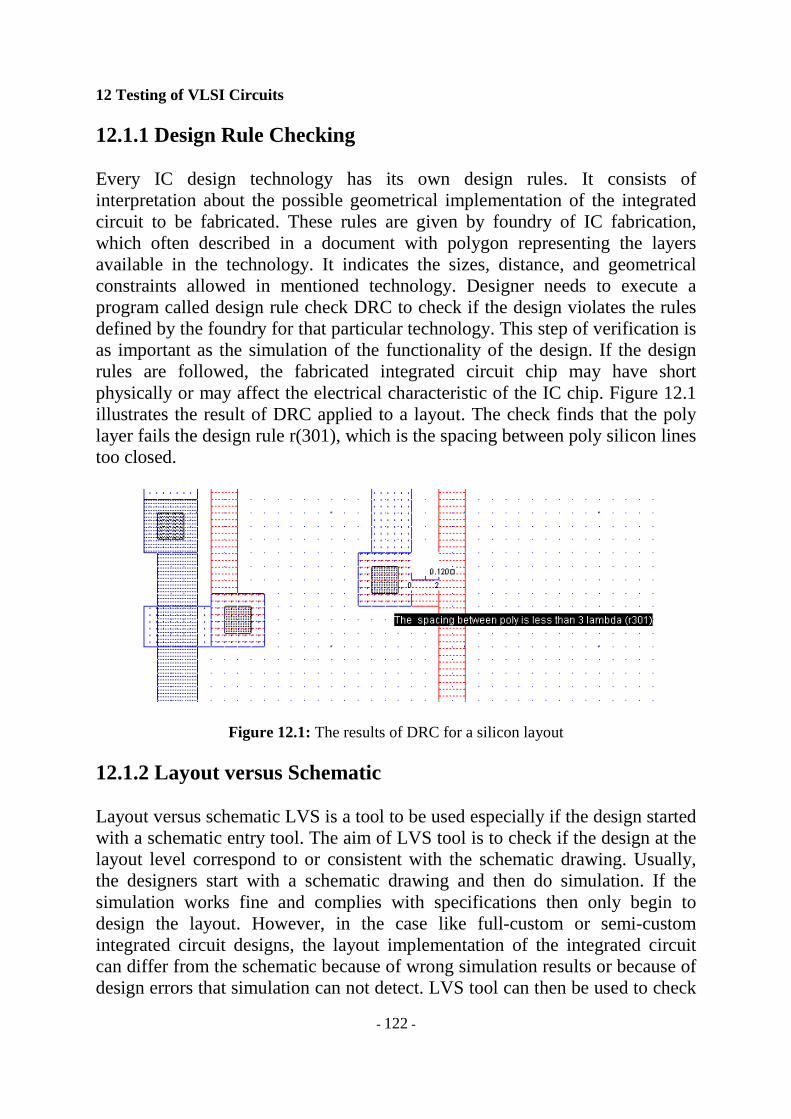
12.1.1 Design Rule Checking Every IC design technology has its own design rules. It consists of interpretation about the possible geometrical implementation of the integrated circuit to be fabricated. These rules are given by foundry of IC fabrication, which often described in a document with polygon representing the layers available in the technology. It indicates the sizes, distance, and geometrical constraints allowed in mentioned technology. Designer needs to execute a program called design rule check DRC to check if the design violates the rules defined by the foundry for that particular technology. This step of verification is as important as the simulation of the functionality of the design. If the design rules are followed, the fabricated integrated circuit chip may have short physically or may affect the electrical characteristic of the IC chip. Figure 12.1 illustrates the result of DRC applied to a layout. The check finds that the poly layer fails the design rule r(301), which is the spacing between poly silicon lines too closed.
Figure 12.1: The results of DRC for a silicon layout
12.1.2 Layout versus Schematic Layout versus schematic LVS is a tool to be used especially if the design started with a schematic entry tool. The aim of LVS tool is to check if the design at the layout level correspond to or consistent with the schematic drawing. Usually, the designers start with a schematic drawing and then do simulation. If the simulation works fine and complies with specifications then only begin to design the layout. However, in the case like full-custom or semi-custom integrated circuit designs, the layout implementation of the integrated circuit can differ from the schematic because of wrong simulation results or because of design errors that simulation can not detect. LVS tool can then be used to check

12 Testing of VLSI Circuits
- 123 -
that if the designer designs the layout according to schematic drawing. To secure better results, a simulation of the layout using the same stimuli used for the schematic is preferred. 12.1.3 Latch-Up and Electrostatic Discharge Latch-up occurred in CMOS device has caused the delay of releasing the CMOS version product to the market in the electronic industry. Latch-up is also called silicon control rectifier SCR effect and it can cause the destruction of the integrated circuit or a part of the integrated circuit. In the severe case, it causes melting of bond wire. There is no real solution to solve this phenomena but a set of design techniques do exist to avoid the occurrence of latch-up such as the design with MOS transistor sitting in its own isolated well and separately isolated the wells with refilled deep trench isolation between the wells as shown in Fig. 12.2.
Figure 12.2: The refilled deep trench isolation between p-well and n-well isolations used to reduce the occurrence of latch-up
The structure of n-MOS and p-MOS transistor has two parasitic diodes form between drain/source and the substrate. An either npn or pnp parasitic bipolar junction transistor formed between drain substrate and source depending on whether it is an n-MOS or p-MOS transistor. In the case of wrong application of stimulant to the device such the input voltage is 0.7V (forward voltage of a diode) greater than the supply voltage VDD. The voltage difference is sufficient to switch-on the emitter-base junction of the parasitic npn bipolar junction transistor. The consequence is the SCR effect result a large current flowing from power supply VDD via a small resistance of collector-emitters of pnpn thyristor structure. This high current will destroy the surrounding p-MOS and n-MOS transistors and can melt the bond wire due high current density.
Beside the isolation technique mentioned earlier to prevent the occurrence of latch-up, other most common technique is to in-activate parasitic bipolar transistor by setting the emitter-base junction of the transistor in reverse bias

12 Testing of VLSI Circuits
- 124 -
mode. This is done by setting the n-well to power supply VDD voltage and setting p-well and p-substrate to VSS rail. These techniques cannot totally eliminate the latch-up problem but it helps reducing its effect. The illustration of these techniques used in the layout is shown in Fig. 12.3.
Figure 12.3: The illustration of n-well and p-substrate bias to prevent occurrence of latch-up
Another electrical constraint of the design is the problem of electrostatic discharge ESD. Owing to very small dimension of the MOS transistor, its ESD susceptibility level is very low. Thus, handling CMOS integrated circuit chip improperly can cause damage to due electrostatic charge generated by human being. One good way is to ground the human being with a ground cord before handling the ESD sensitive CMOS integrated circuit. Besides handling procedure, the designer designs in the ESD protection circuit connecting the input and the inner core circuit. A simple scheme is to connect two diodes at each input one connecting supply voltage VDD and one connecting to VSS rail. These two diodes protect the inner CMOS transistor from ESD damage by discharging the excessive charge to either VSS or VDD. There are many other protection schemes for integrated circuit against ESD. Methods such as design in current limiting resistor, gate-grounded p-MOS and n-MOS transistors, thick oxide MOS device, low voltage triggering silicon control rectifier etc., at the input pad of the device.

12 Testing of VLSI Circuits
- 125 -
12.1.4 Electrical Rule Checking Electrical rule check ERC helps the designer to consider all the minimum necessary implementations for a fee electrical free fault design. This tool verifies that the designer has used a sufficient number of well biases, design in appropriate ESD protection, used VDD and VSS at the right places etc.
12.2 Testing Concepts Testing is a process at the back-end after fabrication of integrated circuit wafer; the integrated circuit chip has been assembled into package form. It is a process whereby the IC device is tested according to the intended application following the device specifications. The intended application can be space/military, industrial, and commercial applications. Thus, the test strategy is to test the device and grade them into four categories that are space/military grade A, industrial grade B, commercial grade C, and failed/reject grade F.
After the integrated circuit has been fabricated, the wafer probe test would screen the die (integrated circuit in chip form) into space/military grade, industrial grade, commercial grade, and of course the non-functional die. The screen test is like picking the best grade students for doctor/engineer professional job, the second best for teacher/lawyer job, and the third best for technician job. The flowchart of the screening test at probe is shown in Fig. 12.4. The test strategy is to test the die with the space/military grade first. If the die fails any of the tests, it is proceeded to test with the industrial test limits. If the die fails any of the industrial limit test, it is then tested with commercial grade test. If the die fails any of the commercial grade tests, it is then yielded as reject. The inking strategy to identify the die grade can be varied. Normally no ink on the surface of the die indicates the die is a space/military grade die. Green is used to identify the industrial grade die. Double inking – red and green, is used to identify the commercial grade die, and red ink is used to identify non-functional - failed to make any specification die. The inking strategy is necessary because the optical system of the die sorting process will pick the die according to the color and categorized them into space/military, industrial, and commercial grade. In the modern approach, inking can be ignored provided there is a grade mapping data of the wafer for each wafer that can be fed to sorter to pick the right grade die.

12 Testing of VLSI Circuits
- 126 -
Figure 12.4: The flowchart of probe test and grading of the die

12 Testing of VLSI Circuits
- 127 -
In the test operation, the process step after assembly, the test strategy follows the same grading systems as it has been described for die probe test. The military grade, industrial grade, and commercial grade device are binned separately by the sorter of automatic test handler ATH. Sorted devices are then branded with the device part number and special digit to signify grading.
Commercial grade device is normally guaranteed to operate for temperature range between 00C to 700C. In order to reduce the cost of testing, the commercial grade device is normally tested with ambient temperature, which is taken as 250C. Since the 00C and 750C temperature tests are not done. The test strategy is to test the device with guard banding for 00C and 750C tests. Commercial product is normally used in the consumer product. The average selling price ASP of the product is low and there are not in critical operation such as a car and commercial plane. Therefore, one ambient with proper guard banding for 00C and 750C tests is sufficient.
Industrial grade device is normally guaranteed to operate for temperature range between -400C to 850C. This grade of product is used in industrial application such as the control system of the car fuel injector etc. Therefore, the test strategy is to test at least two temperatures i.e. ambient and -400C cold temperature. Depending on the criticality of the industrial operation, the product may have to be subjected to an accelerated burn-in to wipe out the infant mortality failure.
Military/space grade device is normally guaranteed to operate for
temperature range between -550C to 1250C. This grade of device is used in space/military application such as the control system of weaponry system. The device normally has to undergo four tests i.e. one ambient before burn-in and three temperature tests after burn-in, which are ambient, +1250C, and -550C tests.
12.3 Automatic Test Equipment, Test Fixture, Test Program, and Automatic Test Handler
To test an integrated circuit – die - after fabrication before package and packaged integrated circuit called device requires at least an automatic test equipment ATE, a test fixture, and a test programs. In the case of automatic testing, an automatic test handler ATE is needed for automatic feeding the device to the test fixture and upon testing automatic categorizes the device into graded type.
12 Testing of VLSI Circuits
- 128 -
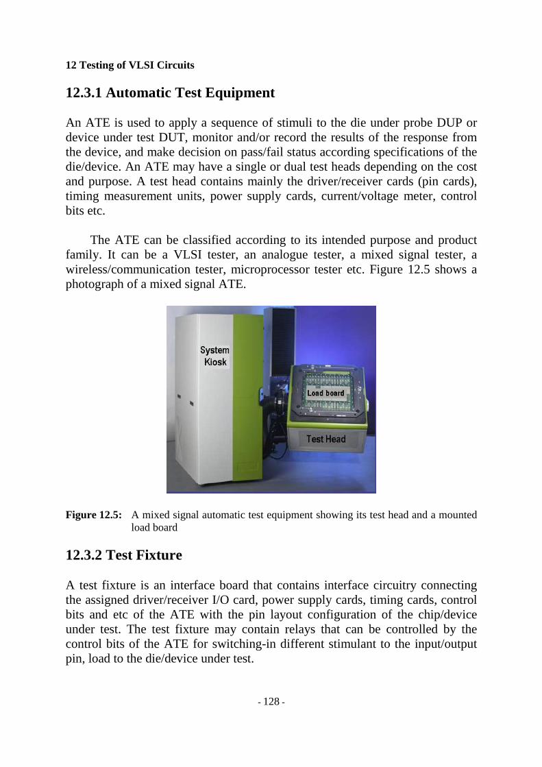
12.3.1 Automatic Test Equipment An ATE is used to apply a sequence of stimuli to the die under probe DUP or device under test DUT, monitor and/or record the results of the response from the device, and make decision on pass/fail status according specifications of the die/device. An ATE may have a single or dual test heads depending on the cost and purpose. A test head contains mainly the driver/receiver cards (pin cards), timing measurement units, power supply cards, current/voltage meter, control bits etc.
The ATE can be classified according to its intended purpose and product family. It can be a VLSI tester, an analogue tester, a mixed signal tester, a wireless/communication tester, microprocessor tester etc. Figure 12.5 shows a photograph of a mixed signal ATE.
Figure 12.5: A mixed signal automatic test equipment showing its test head and a mounted load board
12.3.2 Test Fixture A test fixture is an interface board that contains interface circuitry connecting the assigned driver/receiver I/O card, power supply cards, timing cards, control bits and etc of the ATE with the pin layout configuration of the chip/device under test. The test fixture may contain relays that can be controlled by the control bits of the ATE for switching-in different stimulant to the input/output pin, load to the die/device under test.

12 Testing of VLSI Circuits
- 129 -
A probe card is a test fixture. It is used to probe the integrated circuit die. A mounted prober containing the probe pins arranged in bond pad layout pattern is used to make contact with the bond pads (bond pad is the input/output, clock input etc. that are to be connect via bond wire to the external world) of the die during probe test. The other end of the prober contains a bundle of wire connecting the prober and the probe card. The wafer is mounted on the x-y table that its x-y position is controlled by the ATE.
A load board is a test fixture used for packaged device testing. For VLSI digital testing, a load board may contain simple configuration wiring between the input/output pins, clock pin, power supply pin etc. with the assigned pin card of the ATE. For VLSI analogue device testing, a more complicated device test fixture is required. The bottom end of the load board contains contact pads when in use they are connected to the assigned pin cards etc of the ATE via spring loaded pins. The top part contains a socket that can be mounted on the automatic test hander ATH for automatic feeding testing or temperature testing. A picture of a load board is shown in Fig. 12.6.
Figure 12.6: A top-view of a load board showing the test socket to be mounted on the ATH at the center of the board
Automatic test equipment requires a test program. The program is normally written in a high-level language for instance the IMAGE language used by Teradyne test system. The test program specifies a set of input test vector patterns and a set of output assertions. If an output does not match the asserted value at the corresponding time, the error logic of the ATE will report an error. Before the test vector patterns and assertions are applied, the test program has to set-up the various attributes of an ATE as the following:

12 Testing of VLSI Circuits
- 130 -
• Set the supply voltage. • Assign mapping between stimulus file signal names and physical ATE
pin cards. • Set the pin cards on the ATE to inputs or outputs their VIL/VOH and
VOL/VOH levels. • Set the clock on the ATE. • Set the input pattern and output assertions timing.
and on a device basis
• Apply supply voltages. • Apply digital stimulus and record responses. • Check responses against assertions • Report and log error.
12.3.3 Automatic Test Handler An IC automatic test handler ATH is responsible for feeding the device to a test fixture mounted to an ATE. Chutes or trays containing packaged device can be used to gravity-feed the device to the handler, which uses a variety of mechanical means to pick the device and place it in the test socket on the load board. The ATE stimulus is then applied to the device and device is binned depending on the grade that it has passed or reject if it fails functional test or device specifications. A photograph of an automatic handler is shown in Fig. 5.7. The pilot light at the top left corner of the handler indicates the operating status of the handler. Green light means the handler is in operation. Yellow light indicates there is fault with the handler such as jamming. Red light indicates the handler stop operation. This is necessary to attract attention of the maintenance crew when assistant is needed.
12 Testing of VLSI Circuits
- 131 -
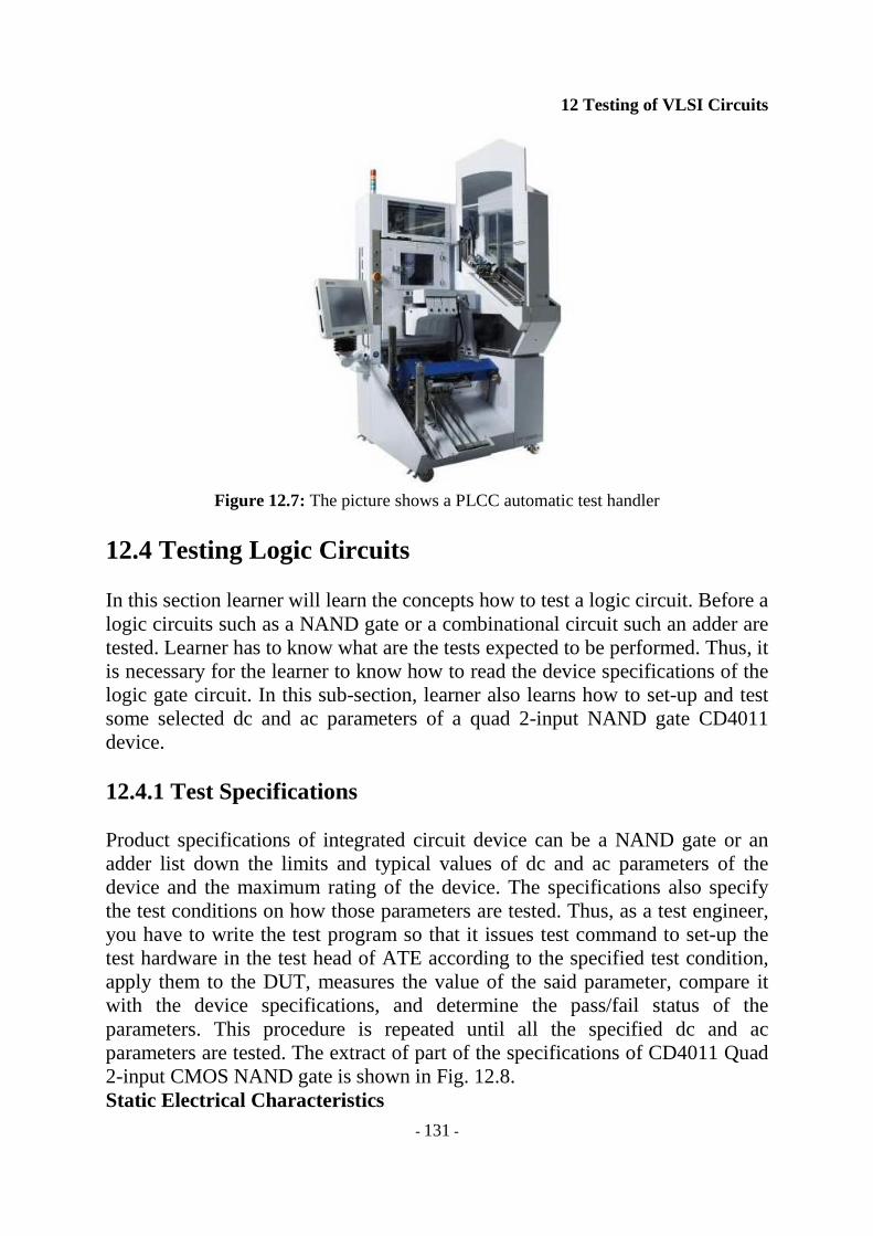
Figure 12.7: The picture shows a PLCC automatic test handler
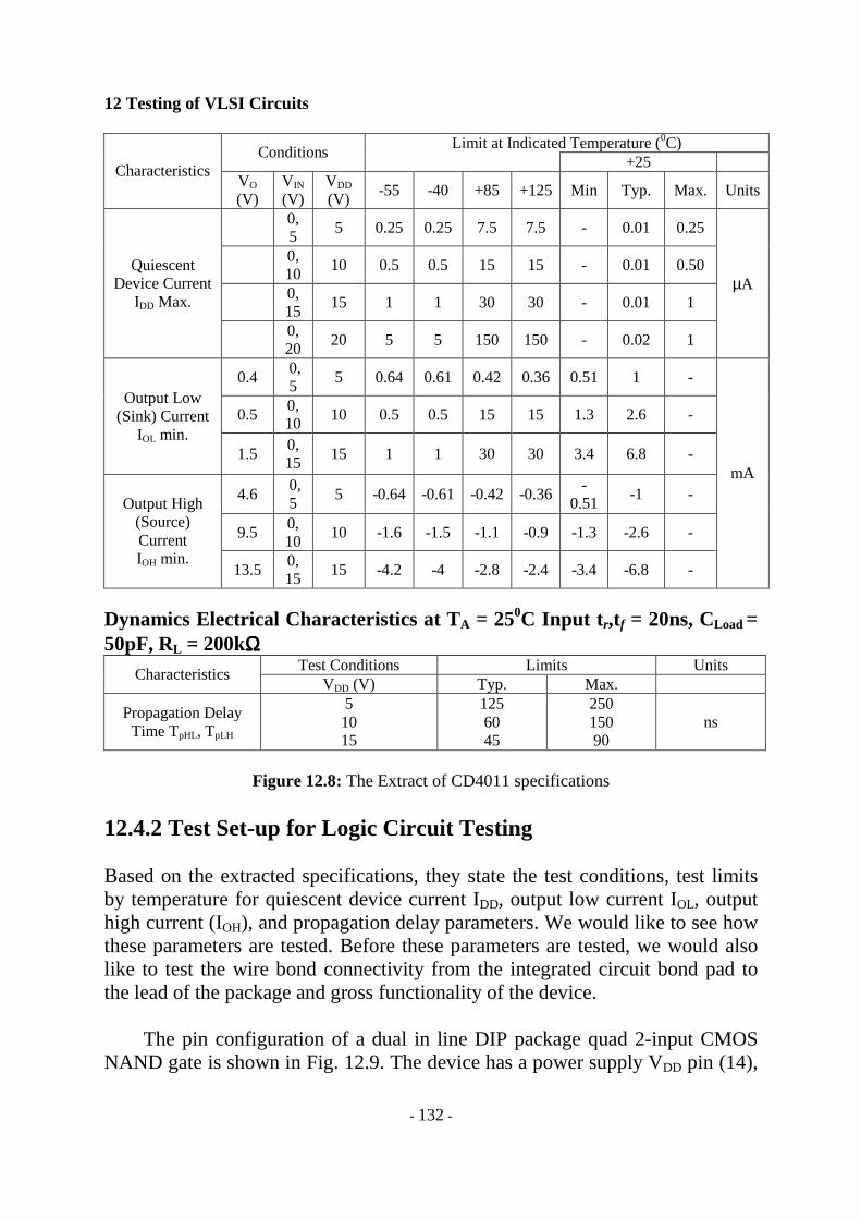
12.4 Testing Logic Circuits In this section learner will learn the concepts how to test a logic circuit. Before a logic circuits such as a NAND gate or a combinational circuit such an adder are tested. Learner has to know what are the tests expected to be performed. Thus, it is necessary for the learner to know how to read the device specifications of the logic gate circuit. In this sub-section, learner also learns how to set-up and test some selected dc and ac parameters of a quad 2-input NAND gate CD4011 device. 12.4.1 Test Specifications Product specifications of integrated circuit device can be a NAND gate or an adder list down the limits and typical values of dc and ac parameters of the device and the maximum rating of the device. The specifications also specify the test conditions on how those parameters are tested. Thus, as a test engineer, you have to write the test program so that it issues test command to set-up the test hardware in the test head of ATE according to the specified test condition, apply them to the DUT, measures the value of the said parameter, compare it with the device specifications, and determine the pass/fail status of the parameters. This procedure is repeated until all the specified dc and ac parameters are tested. The extract of part of the specifications of CD4011 Quad 2-input CMOS NAND gate is shown in Fig. 12.8. Static Electrical Characteristics
12 Testing of VLSI Circuits
- 132 -
Limit at Indicated Temperature (0C) Conditions
+25 Characteristics VO (V)
V IN (V)
VDD (V)
-55 -40 +85 +125 Min Typ. Max. Units
0, 5
5 0.25 0.25 7.5 7.5 - 0.01 0.25
0, 10
10 0.5 0.5 15 15 - 0.01 0.50
0, 15
15 1 1 30 30 - 0.01 1
Quiescent Device Current
IDD Max.
0, 20
20 5 5 150 150 - 0.02 1
µA
0.4 0, 5
5 0.64 0.61 0.42 0.36 0.51 1 -
0.5 0, 10
10 0.5 0.5 15 15 1.3 2.6 - Output Low
(Sink) Current IOL min.
1.5 0, 15
15 1 1 30 30 3.4 6.8 -
4.6 0, 5
5 -0.64 -0.61 -0.42 -0.36 -
0.51 -1 -
9.5 0, 10
10 -1.6 -1.5 -1.1 -0.9 -1.3 -2.6 -
Output High (Source) Current IOH min.
13.5 0, 15
15 -4.2 -4 -2.8 -2.4 -3.4 -6.8 -
mA
Dynamics Electrical Characteristics at TA = 250C Input tr,tf = 20ns, CLoad = 50pF, RL = 200kΩΩΩΩ
Test Conditions Limits Units Characteristics
VDD (V) Typ. Max.
Propagation Delay Time TpHL, TpLH
5 10 15
125 60 45
250 150 90
ns
Figure 12.8: The Extract of CD4011 specifications
12.4.2 Test Set-up for Logic Circuit Testing Based on the extracted specifications, they state the test conditions, test limits by temperature for quiescent device current IDD, output low current IOL, output high current (IOH), and propagation delay parameters. We would like to see how these parameters are tested. Before these parameters are tested, we would also like to test the wire bond connectivity from the integrated circuit bond pad to the lead of the package and gross functionality of the device.
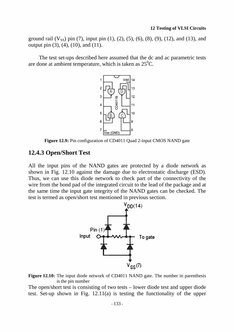
The pin configuration of a dual in line DIP package quad 2-input CMOS NAND gate is shown in Fig. 12.9. The device has a power supply VDD pin (14),
12 Testing of VLSI Circuits
- 133 -
ground rail (VSS) pin (7), input pin (1), (2), (5), (6), (8), (9), (12), and (13), and output pin (3), (4), (10), and (11).
The test set-ups described here assumed that the dc and ac parametric tests
are done at ambient temperature, which is taken as 250C.
Figure 12.9: Pin configuration of CD4011 Quad 2-input CMOS NAND gate
12.4.3 Open/Short Test All the input pins of the NAND gates are protected by a diode network as shown in Fig. 12.10 against the damage due to electrostatic discharge (ESD). Thus, we can use this diode network to check part of the connectivity of the wire from the bond pad of the integrated circuit to the lead of the package and at the same time the input gate integrity of the NAND gates can be checked. The test is termed as open/short test mentioned in previous section.
Figure 12.10: The input diode network of CD4011 NAND gate. The number in parenthesis
is the pin number The open/short test is consisting of two tests – lower diode test and upper diode test. Set-up shown in Fig. 12.11(a) is testing the functionality of the upper

12 Testing of VLSI Circuits
- 134 -
diodes and the wire connecting the bond pads and leads of the package by forcing 1.0mA of current from ATE to the every input pin and then measure the voltage across the input pin with respect to VDD pin. The value measured should be the forward voltage of a diode, which has a value >0.7V. The set-up to test the functionality of lower diodes and the wire connectivity is shown in Fig. 5.11(b). It is done by sinking 1.0mA of current from ATE to the input pin and measure the voltage between input pin and VSS pin. The measured value should be the forward voltage of a diode, which should have a value <- 0.7V. Note that for both tests, the power supply VDD pin (14) and VSS ground rail pin (7), are set to 0V.
(a)
(b)
Figure 12.11: The set-up for open/short test for input pin 1 of CD4011 quad 2-input NAND gate
If there is a shorted diode, the measured voltage will be zero in both tests. Likewise if there is open circuit such as open diode or no connection between bond pad and lead, the voltage measurement should be the maximum value of

12 Testing of VLSI Circuits
- 135 -
the voltage range set by the test program, which can be 2.047V for the case of 2.0V range setting. Thus, as a test engineer, you may to set the test limit as < 0.5V and > -0.5V for short circuit and < -1.5V and > 1.5 for open circuit, and the in between values as good. If there is an open wire connecting VDD or VSS bond pads and leads, all the tests will show as open failure. If the device fails any one of the open/short test, the test program will issue command to halt the test and issue to command to the automatic test handler ATH to yield the device as reject. If the device passes all open/short test except the for output pins. The program will execute the command to proceed to next test. 12.4.4 Gross Functional Test Gross functional test is used to test the functionality of the logic gate before tedious dc and ac tests are performed because there is no point to test the device if there is cross failure such as short-at-VDD, broken metal interconnect in the inner core of the device. For the case of CD4011 NAND gate, the gross functional test tests the logical NAND output of all the input logic combinations. The test set-up for a NAND gate is shown in Fig. 12.12. The remaining 3 NAND can be simultaneously tested if there are sufficient pin cards in the ATE.
Figure 12.12: The set-up for gross functional test of a NAND gate of CD4011
Before the beginning of the gross functional test, the sequence test vector patterns and expected output test vector patterns are programmed into the memory of the ATE. The VSS is set to 0V and VDD is set to 5.0V by the ATE. The pattern generator of the ATE issues test vector 0011 and 0101 sequentially to inputs pin (1) and (2) of the NAND gate via the drivers of the pin cards. The actual output patterns are then compared with the expected output patterns after a programmed propagation delay and input to error logic of ATE to decide whether the gate passes or fails gross functional test.

12 Testing of VLSI Circuits
- 136 -
12.4.5 Quiescent Device Current Test According to the device specifications, the quiescent device current (IDD) test is to be done for four power supply VDD applications, which are 5V, 10V, 15V, and 20V. There are altogether eight measurements to be made. Each supply voltage has two measurements one for all input tie to logic 0 and one all input tie to logic 1.
The set-up for the IDD test is shown in Fig. 12.13. The setting of the logic 1 follows the setting of the power supply (VDD). If the power supply (VDD) is set to 15V, then logic 1 shall be 15V. Logic 0 shall mean 0V. The IDD current is measured by the ampere meter of the power supply. The measured voltage is then compared with the limits of IDD, which are <0.25µA @5V VDD, < 0.5µA @10V VDD, < 1.0µA @10V VDD, and < 1.0µA @20V VDD respectively.
Figure 12.13: The set-up for IDD test for a NAND gate of CD4011 12.4.6 Output Low Current Test From the specifications of device, the output low current IOL is output sink current of the to the n-MOS network of the device when output is at logic 0. For a 2-input NAND gate, there is only one input logic combination that the output is logic 0, which is when both inputs of the gate are at logic 1. According to the specifications of the device, there are three supply voltage applications to be tested, which are 5.0V, 10, and 15V. For each supply voltage test, the output
12 Testing of VLSI Circuits
- 137 -
force voltage is different, which are 0.4V, 0.5V, and 1.5V respectively for supply voltage 5V, 10V, and 15V test. Figure 12.14 shows the test set-up of IOL test for one NAND gate. Normally all NAND gates can be tested simultaneously.
Figure 12.14: The set-up for output low current IOL test
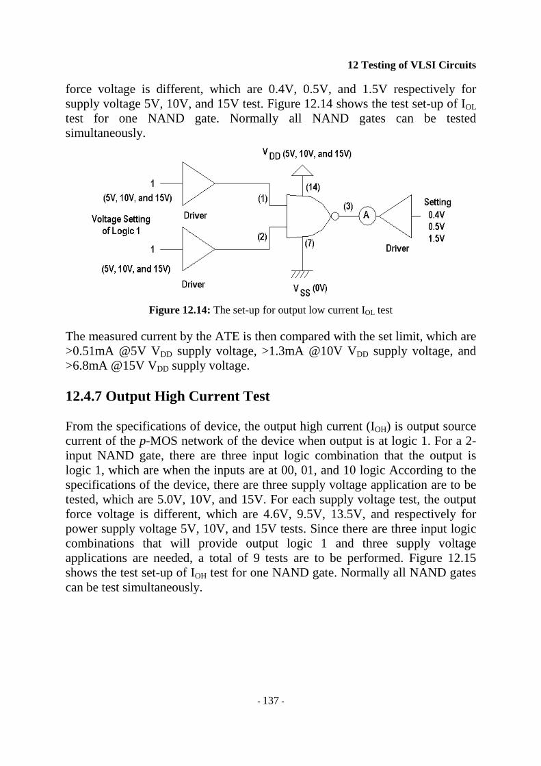
The measured current by the ATE is then compared with the set limit, which are >0.51mA @5V VDD supply voltage, >1.3mA @10V VDD supply voltage, and >6.8mA @15V VDD supply voltage. 12.4.7 Output High Current Test From the specifications of device, the output high current (IOH) is output source current of the p-MOS network of the device when output is at logic 1. For a 2-input NAND gate, there are three input logic combination that the output is logic 1, which are when the inputs are at 00, 01, and 10 logic According to the specifications of the device, there are three supply voltage application are to be tested, which are 5.0V, 10V, and 15V. For each supply voltage test, the output force voltage is different, which are 4.6V, 9.5V, 13.5V, and respectively for power supply voltage 5V, 10V, and 15V tests. Since there are three input logic combinations that will provide output logic 1 and three supply voltage applications are needed, a total of 9 tests are to be performed. Figure 12.15 shows the test set-up of IOH test for one NAND gate. Normally all NAND gates can be test simultaneously.

12 Testing of VLSI Circuits
- 138 -
Figure 12.15: The set-up for output high current IOH test
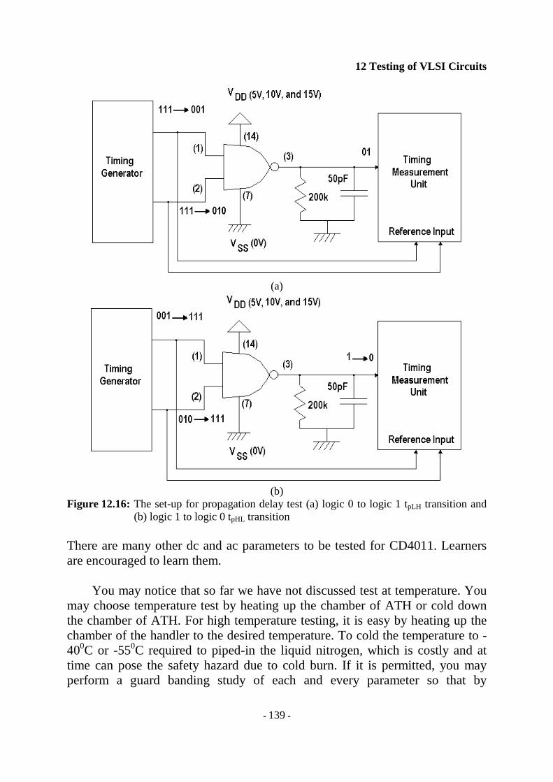
The measured current by the ATE is then compared with the set limit, which are <-0.51mA @5V VDD supply voltage, <-1.6mA @10V VDD supply voltage, <-1.6mA @10V VDD supply voltage, and <-3.4mA @15V VDD supply voltage. 12.4.8 Propagation Delay Test Propagation delay test is a dynamic test or at time it is called ac test. The test requires the timing measurement unit of the ATE. The timing measurement unit of ATE needs to have the rise/fall time better than what is specified in the device specification, which is better than 20ns. There are two tests to be done, which are logic 0 to logic 1tpLH and logic 1 to logic 0 tpHL transitions. According to the truth table of the NAND gate, there are three input logic combinations for transition from logic 0 to logic 1, which are 11→00, 11→01, and 11→10 transition; three input logic combinations for logic 1 to logic 0 transition, which are 00→11, 01→11, and 10→11 transitions. Since there are three power supply applications i.e. 5V, 10V, and 15V, thus, the total number of test are 18. The set-up for the test is shown in Fig. 12.16. The timing generator will generator the required logic state for the input and the timing measurement unit will measure propagation delay and compared it with the set limit, which are <200ns @5V VDD, <100ns<10V VDD, and <80ns @15V VDD.
12 Testing of VLSI Circuits
- 139 -
(a)
(b)
Figure 12.16: The set-up for propagation delay test (a) logic 0 to logic 1 tpLH transition and (b) logic 1 to logic 0 tpHL transition
There are many other dc and ac parameters to be tested for CD4011. Learners are encouraged to learn them.
You may notice that so far we have not discussed test at temperature. You may choose temperature test by heating up the chamber of ATH or cold down the chamber of ATH. For high temperature testing, it is easy by heating up the chamber of the handler to the desired temperature. To cold the temperature to -400C or -550C required to piped-in the liquid nitrogen, which is costly and at time can pose the safety hazard due to cold burn. If it is permitted, you may perform a guard banding study of each and every parameter so that by

12 Testing of VLSI Circuits
- 140 -
tightening the test limits at room temperature can simulate the failure at either cold or hot temperature.
12.5 Designs for Testability
A new piece of equipment, when it is received by the customer, the customer expects it to work without any failure. However, a modern automated equipment such as an automatic test equipment that we use to test the integrated circuit, it is impossible for the an equipment manufacturer to guarantee that every single equipment produced will be working perfectly as it is intended when the test company receive it. Some equipment may not be working because they contain individual components failure or printed circuit board that contain sub-system such as a nano-ammeter are faulty or it may be due to handling leading to failure. Most equipment manufacturers prefer to resolve these problems in the factory, rather than the failure found at customer, which is a bad reputation to the manufacturer.
In the device process cycle, a fault can be occurred at integrated circuit level. If the test strategy is considered at the beginning of the design phase, the fault can be detected rapidly and eliminated at very low cost. When the device is soldered on PCB, the cost for ratification is escalated to ten folds. This is the famous saying Rule of Ten. This cost factors continues to apply until the system has been assembled, packed, and sent to end-user.
The most basic test is testing the functionality of the components, functionality of sub-system printed circuit board. The diagnostic test can be performed to test the 100.0% functionality of the equipment as while system and also be used to identify and locate the particular sub-system failure. If the equipment passes the test, it can be then shipped to customer; otherwise, detailed troubleshooting should be done to identify the failure. It is then follow by either repair or replace the component/board and performance diagnostic test again to ensure this time the equipment is functioning.
The design for testability DFT is a method designed to test the components,
sub-system, and the equipment thorough and less costly with controllability and observability, without the needs to apply full test vectors to the logic gate/circuit, sub-system, and system. This method can identify, detect, and locate failure easily right at circuit design level to a sub-system/system levels. This method has many benefits. The functional test is more reliable; the diagnostic tests run faster and produce more accurate result, and both functional test and diagnostic test require less test-engineering time to develop. The disadvantage is the

12 Testing of VLSI Circuits
- 141 -
engineering effort taken to add in DFT test circuitry in the integrated circuit die and the circuitry would take up a portion of real estate of the die. However, this can be offset by long-term benefit in time taken to identify failure and less development cost for the equipment.
In this Section, learner will learn methods of design for test (DFT), which includes the fault models, in-Circuit testing, ad hoc testing, scan test, and built-in self test. There are many advanced DFTs for testing to identify and locate failure for controllability and observability. Learner is encouraged learn them. 12.5.1 Fault Models As you already know that logic circuits are tested by applying test vectors which consist of input combination and expected output combinations. A logic circuit passes the test if its outputs match what’s expected. In the worst case, an n-input combinational circuit requires 2n test vectors. Take for an example, 2-input NOR gate requires 22 test vectors applied to the input in order to fully knowing the output logic. However, if we know the physical layout of the circuit and make some assumptions about the type of failures that may occur, the number of vectors required to test the circuit fully can be greatly reduced.
There are many models that can be used to describe the failure of the logic circuit. Among the models are; the stuck-at-fault model, stuck-open fault model, bridging fault model, transition delay model, path delay model etc. Stuck-at-open fault model is used to model the behavior of a circuit with transistor are permanently switch-off or switch-on. A bridging fault model is used to model the shorting of two or more signal lines in the circuit. The transition delay model is based on stuck-at fault model. The stuck-at-0 or stuck-at-1 values are replaced by logic 0-to logic 1 and logic 1-to-logic 0 transitions. The path delay model is targeted on total path transition delay. We shall emphasize on the stuck-at-fault model.
The most common model used for testing of the logic circuit is the stuck-
at-fault model which has assumption that all failures cause nodes to be “stuck-at” either logic 0 or logic 1, i.e. either shorted permanently to power supply (VDD) or VSS (GND). This shall mean either a single input or an output signal stuck at logic 0 or logic 1. The assumption made is true and the method work well in actual practice condition. Figure 12.17 illustrates the meaning of a stuck-at-0 and stuck-at-1 with a 2-input NOR gate. The input B shorted to power supply VDD is termed as stuck-at-1, while the input A shorted to VSS is termed

12 Testing of VLSI Circuits
- 142 -
as stuck-at-0. The suck-at-0 and stuck-at-1 can also be happened at the output of the device.
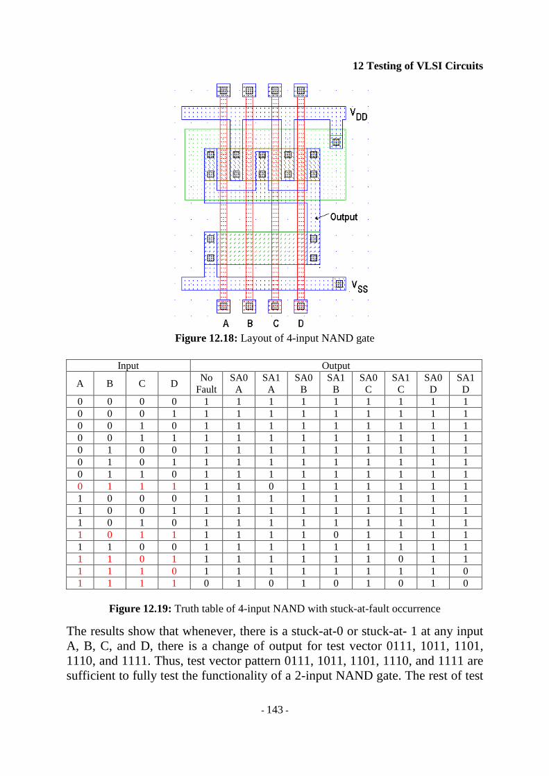
Using the stuck-at-fault model, let’s analyse to see how many test vector patterns are necessary to effectively test the functionality of a 4-input NAND gate. The layout of the 4-input NAND gat is shown in Fig. 12.18. Based on the layout, stuck-at-0 (SA0) and stuck-at-1 (SA1) faults can be occurred at either input A, B, C, or D, or all inputs, and output.
Figure 12.17: Illustrating meaning of stuck-at-0 and stuck-at-1
Theoretically, it requires 16 (24) test vector patterns in order to fully test its functionality. However, if we apply the stuck-at-fault method, the 4-input NAND can be fully tested with just five test vector patterns, which are 1111, 0111, 1011, 1101, and 1110. Let’s find out how we derive to this conclusion. The truth table of a 4-input NAND gate with stuck-at-fault occurrence is shown in Fig. 12.19.
12 Testing of VLSI Circuits
- 143 -
Figure 12.18: Layout of 4-input NAND gate
Input Output
A B C D No
Fault SA0 A
SA1 A
SA0 B
SA1 B
SA0 C
SA1 C
SA0 D
SA1 D
0 0 0 0 1 1 1 1 1 1 1 1 1 0 0 0 1 1 1 1 1 1 1 1 1 1 0 0 1 0 1 1 1 1 1 1 1 1 1 0 0 1 1 1 1 1 1 1 1 1 1 1 0 1 0 0 1 1 1 1 1 1 1 1 1 0 1 0 1 1 1 1 1 1 1 1 1 1 0 1 1 0 1 1 1 1 1 1 1 1 1 0 1 1 1 1 1 0 1 1 1 1 1 1 1 0 0 0 1 1 1 1 1 1 1 1 1 1 0 0 1 1 1 1 1 1 1 1 1 1 1 0 1 0 1 1 1 1 1 1 1 1 1 1 0 1 1 1 1 1 1 0 1 1 1 1 1 1 0 0 1 1 1 1 1 1 1 1 1 1 1 0 1 1 1 1 1 1 1 0 1 1 1 1 1 0 1 1 1 1 1 1 1 1 0 1 1 1 1 0 1 0 1 0 1 0 1 0
Figure 12.19: Truth table of 4-input NAND with stuck-at-fault occurrence
The results show that whenever, there is a stuck-at-0 or stuck-at- 1 at any input A, B, C, and D, there is a change of output for test vector 0111, 1011, 1101, 1110, and 1111. Thus, test vector pattern 0111, 1011, 1101, 1110, and 1111 are sufficient to fully test the functionality of a 2-input NAND gate. The rest of test
12 Testing of VLSI Circuits
- 144 -
vectors 0000, 0001, 0010, 0011, 0100, 0101, 0110, 1000, 1001, 1010, and 1100 are redundant.
Under the stuck-at-fault model, it’s easy to apply test vectors to the input of an individual logic gate. However, in practice, there is problem to apply the test vectors to the logic gates that are buried in a circuit and observing the results. Supposing a circuit has a few combinational and sequential logic gates in between its primary inputs and the inputs of a 4-input NAND gate that a designer wants to test, it is not obvious what primary-input test vector, or sequence of primary-input test vectors must be applied to generate the test vector pattern 1111 at the NAND-gate inputs. Furthermore, it’s not obvious what else is required to propagate the NAND gate’s output to a primary output of the circuit.
Sophisticated test-generation program deals with this complexity and
attempt to create a complete test set for a circuit, which is a sequence of test vector patterns that fully tests each logic gate in the circuit. However, the computation required can be huge and it’s quite often just not possible to generate a complete test vector patterns. With this difficulty, DFT methods attempt to simplify test-pattern generation by enhancing the controllability and observability of logic gates in a circuit. A circuit with good controllability and easy to produce any desired output logic on the internal signals of the circuit by applying an appropriate test-vector input combination to the primary inputs is desired. Similarly, a circuit with good observability means that any internal signal can be easily propagated to a primary output for comparison with an expected value by the application of an appropriate primary-input combination is needed. The most common method of improving controllability and observability is to add test points to tap the additional primary inputs and outputs during testing.
12.5.2 Ad Hoc Testing Ad hoc test techniques are temporary test procedure added on the need basis aimed at reducing the number of combinational pattern of testing. They are only useful for small designs where scans, automatic test pattern generator ATPG, built-in self test BIST are not available. However, a completed scan-based testing methodology is recommended for all logic circuits. The common techniques for ad hoc testing are partitioning large sequential test, adding test point, adding multiplexer, and providing for easy state reset.

12 Testing of VLSI Circuits
- 145 -
A technique classified in this category is the use of the bus in a bus-oriented system for test purposes. Each register has been made loadable from the bus and capable of being driven onto the bus. Here, the internal logic values that exist on a data bus are enabled onto the bus for testing purpose. Frequently, multiplexer can be used to provide alternative signal path during testing. In CMOS testing, transmission gate and multiplexers provide alternative paths to routed external test signals. We can see it in the built-in circuit of the scan test and built-in self test.
Any design should always have a method of resetting the internal state of
the circuit within single clock cycle or at most a few clock cycles. Apart from making the testing easier, this also makes simulation faster as a few cycles are required to initialize the circuit is considered short time.
In general, ad hoc testing techniques represent a number of approaches
developed over the years by designers to avoid the overhead of a systematic approach to testing. While these general approaches are still valid as of today. 12.5.3 In-Circuit Testing The logic circuits in terms of IC package are mounted on a single PCB. The controllability and observability of the circuits ultimately can be obtained by using every pin of every IC as a test point and route them to the edge connector of the PCB so that they can be tested. This is then followed by building a special test fixture that matches the edge connector layout of the PCB. The PCB is placed on the spring loaded pins of test fixture (load board) and is connected to automatic test equipment that can monitor each pin as required by a test program.
In-circuit testing also can achieve the ultimate goal of controllability. This method not only can monitor the signals at the spring loaded pins for observability, but also connects loaded pin to a very low impedance driving circuit in the ATE. In this way, the tester can override whatever circuit on the PCB normally drives each signal, and directly generate any desired test vector pattern on the internal signals of the circuit in PCB. Overdriving an opposing gate output causes excessive current flow in both the tester and the opposing gate, but the tester can sink the current within a few milli-seconds, which is not harmful to the circuit.
To test an 4-input NAND gate, an in-circuit tester needs only to provide the
five test vectors mentioned previously and can ignore whatever values that the
12 Testing of VLSI Circuits
- 146 -
rest of the circuit is trying to drive onto the four input pins. The output of 4-input NAND-gate can be observed directly on the output pin. With in-circuit testing, each logic gate can be tested in isolation from the others.
A few key procedures and requirement are needed for performing in-circuit
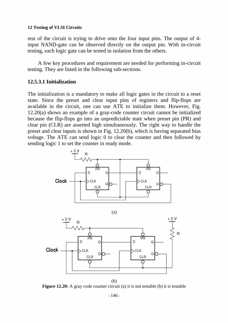
testing. They are listed in the following sub-sections. 12.5.3.1 Initialization The initialization is a mandatory to make all logic gates in the circuit to a reset state. Since the preset and clear input pins of registers and flip-flops are available in the circuit, one can use ATE to initialize them. However, Fig. 12.20(a) shows an example of a gray-code counter circuit cannot be initialized because the flip-flops go into an unpredictable state when preset pin (PR) and clear pin (CLR) are asserted high simultaneously. The right way to handle the preset and clear inputs is shown in Fig. 12.20(b), which is having separated bias voltage. The ATE can send logic 0 to clear the counter and then followed by sending logic 1 to set the counter in ready mode.
(a)
(b)
Figure 12.20: A gray code counter circuit (a) it is not testable (b) it is testable

12 Testing of VLSI Circuits
- 147 -
12.5.3.2 Clock generation The ATE must be able to provide its own clock signal without depending on the on-board clock signals. For several reasons, ATE usually must override an on-board clock, which are the speed at which it can apply the test vectors is limited; it must allow extra time for overdriven signals to settle; and sometimes it must stop the clock. However, overdriving the clock may oscillate the circuit and make several transitions between logic 0 and logic 1 before finally settling to the desire level.
Figure 12.21 shows a recommended clock driver circuit. To inject its own clock, the tester pulls Clk En to logic 0 and inserts its clock on TestClk_L pin. Since the ATE is not overdriving any gate outputs, the resulting clock signal is clean. In general, any normally glitch-free signal used as a clock input or other asynchronous input must not be overdriven by the tester, and would have to be treated in a way similar what is shown in Fig. 12.21. This is another reason why synchronous design with a single clock is desirable.
Figure 12.21: A clock drive for in-board testing
12.5.3.3 Grounded inputs In general, ground should not be permanently tied to zero volt source. For the in-circuit testing, ATE must be able change the voltage level of this signal. Therefore, signals that require a zero volt input during normal operations should be tied to ground through a resistor, which allows the ATE to set it to logic 1 by connecting the supply voltage VDD. 12.5.3.4 Bus drivers In general, it should be possible to disable the drivers for wide buses so that the ATE can drive the bus without having to overdrive all the signals on the bus. That is, it should be possible to output-disable all of the tri-state drivers on a bus, so that the tester drives an open bus. This reduces electrical stress both on the ATE and output of the devices in the PCB. Otherwise overheat due excessive

12 Testing of VLSI Circuits
- 148 -
current driven the output may damage by having all outputs overdriven simultaneously. 12.5.4 Scan Testing In-circuit testing works fine, up to a point. It doesn’t do much good for custom VLSI chips and application specific IC ASIC, because the internal signals simply are not accessible. Even in board-level circuits, high-density packaging technologies such as surface mounting greatly increase the difficulty of providing test points for every signal on a PCB. As a result, an increasing number of designs are using scan testing to provide controllability and observability.
A scan testing provides controllability and observability of the internal signals of a circuit using a small number of test points. A scan-path method considers any digital circuit to be a collection of flip-flops or other storage elements interconnected by combinational logic gate. It is a concerned with controlling and observing the state of the storage elements. It does this by providing two operating modes, which are a normal mode, and a scan mode in which all of the storage elements are reorganized into a giant shift register. In scan mode, the state of the circuit’s n storage elements can be read out by n shifts thus, providing observability, and a new state can be loaded at the same time that shows controllability. Scan-path design is used most often in custom VLSI and ASIC designs because of the impossibility of providing a large number of conventional test points.
Let’s consider a 3-bit binary counter as shown in Fig. 12.22. The circuit consists of two parts, which are combinational logic circuit blocks and three D flip-flops. This circuit has limited observability and controllability. To complete testing this circuit fully, it requires 22x23 = 32 test vector patterns, which comprising of enable, reset and 8 clock pulses. The timing of the test is shown in Fig. 12.23.

12 Testing of VLSI Circuits
- 149 -
Figure 12.22: A 3-bit binary counter
Figure 12.23: The timing diagram of the test for a 3-bit binary counter The circuit has three combinational circuit blocks. Every block has its input and output. The MSB combinational block at the right of the circuit received 3 inputs I0, I1, I2 and has one output CO2. If we have the controllability of node Io and observability at node CO2 then we can have easily test the functionality of this circuit block by applying the minimum number of test vectors (based on to stuck-at-fault model) to it. Thus, the key issue is to make I0, I1, I2 control-able
12 Testing of VLSI Circuits
- 150 -
via the chip boundary and CO2 observable via the chip boundary. We will do similar kind of arrangements for all inputs and outputs to all the combinational blocks identified in the design.
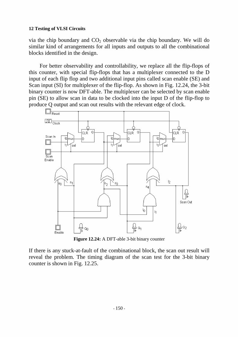
For better observability and controllability, we replace all the flip-flops of this counter, with special flip-flops that has a multiplexer connected to the D input of each flip flop and two additional input pins called scan enable (SE) and Scan input (SI) for multiplexer of the flip-flop. As shown in Fig. 12.24, the 3-bit binary counter is now DFT-able. The multiplexer can be selected by scan enable pin (SE) to allow scan in data to be clocked into the input D of the flip-flop to produce Q output and scan out results with the relevant edge of clock.
Figure 12.24: A DFT-able 3-bit binary counter
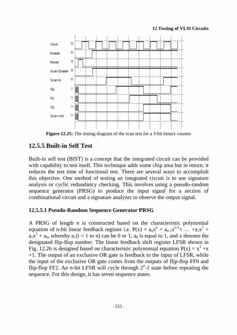
If there is any stuck-at-fault of the combinational block, the scan out result will reveal the problem. The timing diagram of the scan test for the 3-bit binary counter is shown in Fig. 12.25.
12 Testing of VLSI Circuits
- 151 -
Figure 12.25: The timing diagram of the scan test for a 3-bit binary counter
12.5.5 Built-in Self Test Built-in self test (BIST) is a concept that the integrated circuit can be provided with capability to test itself. This technique adds some chip area but in return, it reduces the test time of functional test. There are several ways to accomplish this objective. One method of testing an integrated circuit is to use signature analysis or cyclic redundancy checking. This involves using a pseudo-random sequence generator (PRSG) to produce the input signal for a section of combinational circuit and a signature analyzer to observe the output signal. 12.5.5.1 Pseudo-Random Sequence Generator PRSG A PRSG of length n is constructed based on the characteristic polynomial equation of n-bit linear feedback register i.e. P(x) = anx
n + an-1xn-1+ … +a2x
2 + a1x
1 + a0, whereby ai (i = 1 to n) can be 0 or 1, a0 is equal to 1, and x denotes the designated flip-flop number. The linear feedback shift register LFSR shown in Fig. 12.26 is designed based on characteristic polynomial equation P(x) = x3 +x +1. The output of an exclusive OR gate is feedback to the input of LFSR, while the input of the exclusive OR gate comes from the outputs of flip-flop FF0 and flip-flop FF2. An n-bit LFSR will cycle through 2n-1 state before repeating the sequence. For this design, it has seven sequence states.
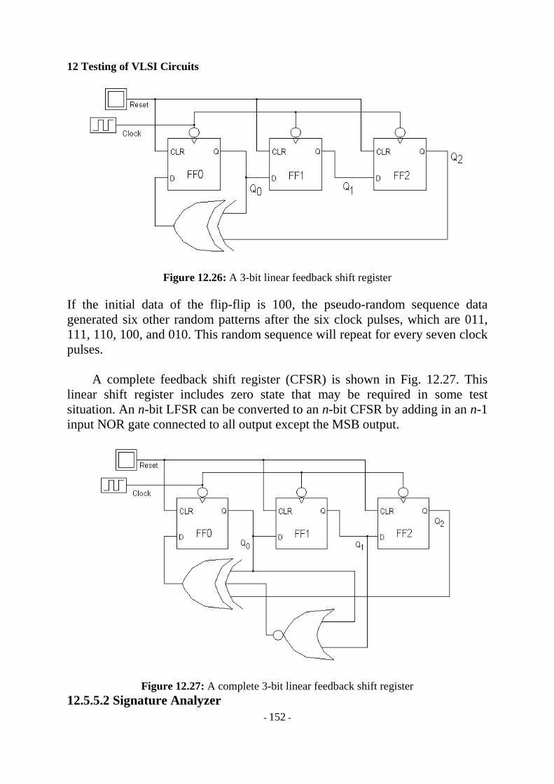
12 Testing of VLSI Circuits
- 152 -
Figure 12.26: A 3-bit linear feedback shift register If the initial data of the flip-flip is 100, the pseudo-random sequence data generated six other random patterns after the six clock pulses, which are 011, 111, 110, 100, and 010. This random sequence will repeat for every seven clock pulses.
A complete feedback shift register (CFSR) is shown in Fig. 12.27. This linear shift register includes zero state that may be required in some test situation. An n-bit LFSR can be converted to an n-bit CFSR by adding in an n-1 input NOR gate connected to all output except the MSB output.
Figure 12.27: A complete 3-bit linear feedback shift register 12.5.5.2 Signature Analyzer
12 Testing of VLSI Circuits
- 153 -
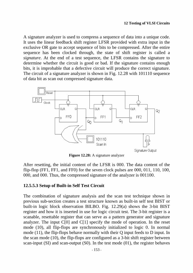
A signature analyzer is used to compress a sequence of data into a unique code. It uses the linear feedback shift register LFSR provided with extra input in the exclusive OR gate to accept sequence of bits to be compressed. After the entire sequence has been clocked through, the state of shift register is called a signature. At the end of a test sequence, the LFSR contains the signature to determine whether the circuit is good or bad. If the signature contains enough bits, it is improbable that a defective circuit will produce the correct signature. The circuit of a signature analyzer is shown in Fig. 12.28 with 101110 sequence of data bit as scan out compressed signature data.
Figure 12.28: A signature analyzer
After resetting, the initial content of the LFSR is 000. The data content of the flip-flop (FF1, FF1, and FF0) for the seven clock pulses are 000, 011, 110, 100, 000, and 000. Thus, the compressed signature of the analyzer is 001100. 12.5.5.3 Setup of Built-in Self Test Circuit The combination of signature analysis and the scan test technique shown in previous sub-section creates a test structure known as built-in self test BIST or built-in logic block observation BILBO. Fig. 12.29(a) shows the 3-bit BIST register and how it is inserted in use for logic circuit test. The 3-bit register is a scanable, resettable register that can serve as a pattern generator and signature analyzer. The input C[0] and C[1] specify the mode of operation. In the reset mode (10), all flip-flops are synchronously initialized to logic 0. In normal mode (11), the flip-flops behave normally with their Q input feeds to D input. In the scan mode (10), the flip-flops are configured as a 3-bit shift register between scan-input (SI) and scan-output (S0). In the test mode (01), the register behaves

12 Testing of VLSI Circuits
- 154 -
as a pseudo-random sequence generator or signature analyzer. If all the D inputs are held at logic 0, the Q outputs loop through a pseudo-random bit sequence, which can serve as input to the combinational logic. If D inputs are taken from the output of combinational logic, they are swizzled with the existing state to produce signature code. In summary BIST is performed by first resetting the content in the output register. Then both registers are placed in the test mode to produce pseudo-random inputs and calculate the expected signature code. Finally, the signature code is shifted out the scan chain. Figure 5.29(b) shows the block diagram of BIST.
(a)
(b)
Figure 12.29: BIST (a) a 3-bit register and (b) PRSG and signature analyzer used for test circuit
There are many other BIST techniques such as memory BIST, parallel BIST, which are not covered in this text. Learner is encouraged to learn them.
12 Testing of VLSI Circuits
- 155 -
12.6 Failure Analysis Failure analysis is important in semiconductor industry because it helps to identify the cause of the failure of the circuit. Knowing the cause of the failure, preventive measure or corrective action can be taken to prevent re-occurrence of the problem. Solving the root cause of the failure shall mean the loss due to failure can be minimized and at the same time, the reliability of the circuit can be ensured in terms of quality assurance.
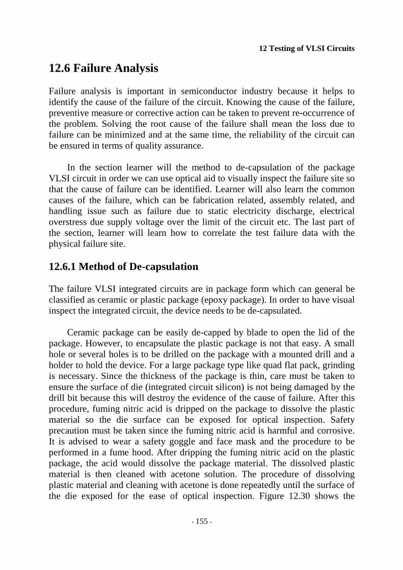
In the section learner will the method to de-capsulation of the package VLSI circuit in order we can use optical aid to visually inspect the failure site so that the cause of failure can be identified. Learner will also learn the common causes of the failure, which can be fabrication related, assembly related, and handling issue such as failure due to static electricity discharge, electrical overstress due supply voltage over the limit of the circuit etc. The last part of the section, learner will learn how to correlate the test failure data with the physical failure site. 12.6.1 Method of De-capsulation The failure VLSI integrated circuits are in package form which can general be classified as ceramic or plastic package (epoxy package). In order to have visual inspect the integrated circuit, the device needs to be de-capsulated.
Ceramic package can be easily de-capped by blade to open the lid of the package. However, to encapsulate the plastic package is not that easy. A small hole or several holes is to be drilled on the package with a mounted drill and a holder to hold the device. For a large package type like quad flat pack, grinding is necessary. Since the thickness of the package is thin, care must be taken to ensure the surface of die (integrated circuit silicon) is not being damaged by the drill bit because this will destroy the evidence of the cause of failure. After this procedure, fuming nitric acid is dripped on the package to dissolve the plastic material so the die surface can be exposed for optical inspection. Safety precaution must be taken since the fuming nitric acid is harmful and corrosive. It is advised to wear a safety goggle and face mask and the procedure to be performed in a fume hood. After dripping the fuming nitric acid on the plastic package, the acid would dissolve the package material. The dissolved plastic material is then cleaned with acetone solution. The procedure of dissolving plastic material and cleaning with acetone is done repeatedly until the surface of the die exposed for the ease of optical inspection. Figure 12.30 shows the
12 Testing of VLSI Circuits
- 156 -
picture of a de-capsulated quad flat pack QFP plastic packaged integrated circuit. It shows that exposed die.
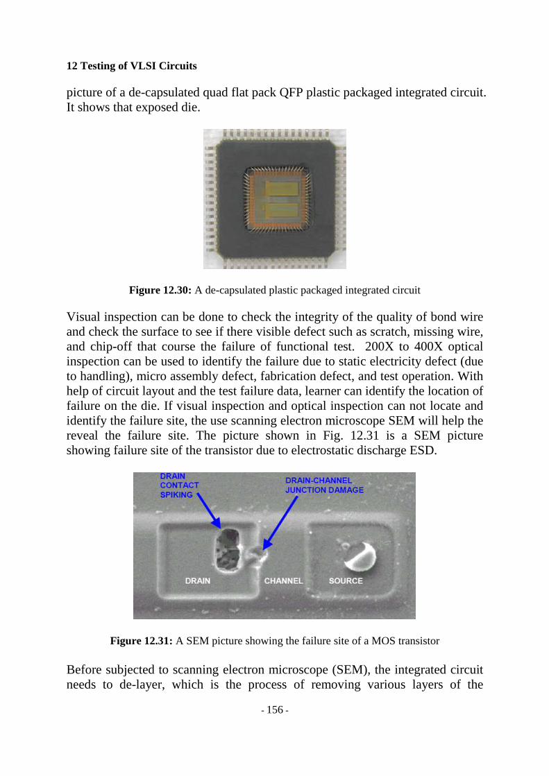
Figure 12.30: A de-capsulated plastic packaged integrated circuit Visual inspection can be done to check the integrity of the quality of bond wire and check the surface to see if there visible defect such as scratch, missing wire, and chip-off that course the failure of functional test. 200X to 400X optical inspection can be used to identify the failure due to static electricity defect (due to handling), micro assembly defect, fabrication defect, and test operation. With help of circuit layout and the test failure data, learner can identify the location of failure on the die. If visual inspection and optical inspection can not locate and identify the failure site, the use scanning electron microscope SEM will help the reveal the failure site. The picture shown in Fig. 12.31 is a SEM picture showing failure site of the transistor due to electrostatic discharge ESD.
Figure 12.31: A SEM picture showing the failure site of a MOS transistor Before subjected to scanning electron microscope (SEM), the integrated circuit needs to de-layer, which is the process of removing various layers of the

12 Testing of VLSI Circuits
- 157 -
integrated circuit such as the glassivation layer, aluminum metallic interconnect layout, and oxide isolation layer , nitride isolation layout and polysilicon layer of integrated circuit. After the removals of these layers, it allows access to the surface of diffusion layer for SEM revelation. 12.6.2 Cause of Failure There are many causes of integrated circuit failure. The most common failure are coming from fabrication, assembly, and handling problem and test overstress problem at test operations. As you already know, for the fabrication of a VLSI circuit, it involves multiply repeated process steps. These process steps can leave multiply problems such as over etch, metal shorting, mask misalignment, residue of photoresist if some of these process steps are out of control, which means it does not comply to process specifications. The mentioned fabrication process problems will cause non-functionality of the integrated circuit either at probe test, a test before assembly used to grossly check the functionality of the integrated circuit and a package final test. Usually the failure will show-up as open and short test failure and gross functional failure.
There are a number of assembly processes, which can be summarized as wafer cutting, die attach, wire bond, encapsulation, environmental test, tin plate/lead soldering, form and trim. All these processes particularly the process before encapsulation, can cause integrated circuit failure due to scratch, chip-off, eutectic attached die lift etc. A scratch on the integrated circuit will cause gross functional failure.
In test operation, the most common causes of the failure are electrostatic
discharge and electric overstress due to improper set-up procedure and sequence in the test program. Proper grounding of the ATE and automatic test handler ATH and grounding of working personnel are necessary to prevent failure due to ESD. 12.6.3 Failure Correlation Since cause of failure at test operation can be from multiply sources. One of the primary ways to identify the failure is from the failure test data. Since the test for an integrated circuit basically consists of open/short test, gross functional test, dc test, and ac test, we can rely on the failure data to determine the cause of the failure. If the device failure open/short test, from the test data, we will know which pin/pins are having either short or open failure. We can then confirm by

12 Testing of VLSI Circuits
- 158 -
de-cap the package for ceramic package or x-ray the plastic package to locate and confirm the failure site. For the case of open/short test, it can be due to missing bond wire or bond wire shorted to adjacent bond wire.
In the case of functional failure like the case of memory array failure, test data will show the address location of failure that can be traced to a particular row and column of memory matrices on the integrated circuit with aid of the layout diagram of the integrated circuit. In this manner, we can correlate the failure data with physical site of failure.
In the case of ac failure, the correlation of failure data cannot be traced to
the physical failure site. This is because the failure is related with the physical parameters of the transistor in the integrated circuit. As you have learnt in Unit 3 – Parasitic Extraction and Performance, they are related to the dimension and particularly the doping concentration, and threshold of the transistor. If such failure occurred, we can check back the data of the process parameters used during fabrication for further understanding of the failure.
Exercises 12.1. State three methods that can be used to minimize of the design constraints
due to latch-up problem.
12.2. As a design engineer you know that there is an npn parasitic bipolar junction transistor in the n-MOS transistor strcuture. Name the method used to in-active this transistor.
12.3. State the reason why there is no diode circuit at the output of the logic
gate to protect against ESD damage. 12.4. The output low voltage (VOL) specification of the CD4011 2-input NAND
gate is given as follow. Draw the test set-up diagram to perform this test.
Limit at Indicated Temperature (0C) Conditions
+25 Characteristics VO (V)
V IN (V)
VDD (V)
-55 -40 +85 +125 Min Typ. Max. Units
- 0, 5 5 0.05 0.05 0.05 0.05 - 0 0.05
- 0, 10 10 0.05 0.05 0.05 0.05 - 0 0.05 Output Low
Voltage VOL max. - 0, 15 15 0.05 0.05 0.05 0.05 - 0 0.05
V
12 Testing of VLSI Circuits
- 159 -
12.5. A combinational circuit has logic function Y= )ED()CBA( +⋅++ , what is the number of test vectors required to fully test the functionally of this logic circuit.
12.6. Using stuck-at-fault method to find the optimum test vector patterns to
test the functionality of the following combinational logic circuit.
12.7. A linear feedback shift register is shown in below. Draw the timing
diagram of the register.
12.8. The signature analyzer circuit shown below in scan in data sequence
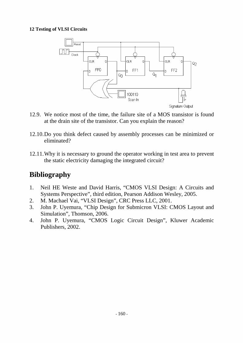
100110. Find the compressed signature out code assuming the initialized content of the analyzer is 000.
12 Testing of VLSI Circuits
- 160 -
12.9. We notice most of the time, the failure site of a MOS transistor is found
at the drain site of the transistor. Can you explain the reason? 12.10. Do you think defect caused by assembly processes can be minimized or
eliminated? 12.11. Why it is necessary to ground the operator working in test area to prevent
the static electricity damaging the integrated circuit?
Bibliography 1. Neil HE Weste and David Harris, “CMOS VLSI Design: A Circuits and
Systems Perspective”, third edition, Pearson Addison Wesley, 2005. 2. M. Machael Vai, “VLSI Design”, CRC Press LLC, 2001. 3. John P. Uyemura, “Chip Design for Submicron VLSI: CMOS Layout and
Simulation”, Thomson, 2006. 4. John P. Uyemura, “CMOS Logic Circuit Design”, Kluwer Academic
Publishers, 2002.

Index
- 161 -
A
Acetone solution ...................................156 Application specific IC .........................149 Automatic test equipment .....................141 Automatic test handler ..........................158 Automatic test pattern generation .........145 Average selling price ............................128
B
Bond pad ...............................................130 Built-in logic block observation............154 Built-in self test.............................145, 152
C
CD4011.................................................132 Ceramic package...................................156 Complete feedback shift register ..........153 Controllability.......................................145
D
Design rule check..................................122 Device specification..............................132 Device under test...................................129 Dual in line............................................133
E
Electrical rule check..............................125 Electrostatic discharge ..........................134
F
Flip-flop ................................................147 Fuming nitric acid .................................156
G
Gray-code counter.................................147 Gross functional test .............................136
I
In-circuit testing....................................146
L
Layout versus schematic check ............123 Linear feedback shift register ...............152 Load board ............................................130
N
NAND gate ...........................................145 NOR gate ..............................................142
O
Observability.........................................145 Open/short test ......................................134 Output high current...............................138 Output low current................................137
P
Probe test ..............................................126 Propagation delay .................................139 Pseudo-Random Sequence Generator ..152
Q
Quad flat pack.......................................157 Quiescent device current.......................137
R
Rule of Ten ...........................................141
S
Scan method..........................................149 Signature analyzer ................................154 Silicon control rectifier .........................123
T
Test fixture....................................130, 146 Test program.........................................128 Test vectors...........................................142

Index
- 162 -