
VLSI Circuits and Systems Letter - IEEE Computer Society...VLSI Circuits and Systems Letter Volume 2...
29
tcvlsi.org VLSI Circuits and Systems Letter Volume 2, Issue 1, April 2016 Editorial Features • Mohit S. Choudhary, Mahesh Kumawat, Pramod K. Bharti, and S. K. Vishvakarma, 16.64Gbps Synchronous CML SerDes Transceiver Design Technique with Process Corner Variations for Low Power Application • Sudeendra Kumar K, Sauvagya Sahoo and K.K.Mahapatra, Review on Post Silicon Validation of Physical Unclonable Functions • Huafeng Yu, Architecture-Centric Integration Challenges for Automotive Cyber-Physical Systems • Aida Todri-Sanial and Chuan Seng Tan, Physical Design for 3D Integrated Circuits Opinions • Theocharis Theocharides, Deep Learning Algorithms – VLSI Friends or Foes? • Prasun Ghosal, Pratima Chatterjee and Mayukh Sarkar, Bringing out a Natural Computer (Ribosome) from within a Cell: A Next-Gen Alternative? • Mary Lourde R, Challenges and Vdvances in FinFET Device Technology Updates • Upcoming Conferences, Workshops and Events • Call for Papers and Proposals • Funding Opportunities • Job Openings • Ph.D. Fellowships Available Outreach and Community • Mike Borowczak and Andrea Burrows, Are We Still Teaching VLSI the Same Way We Were in the Mid-90s? Call for Contributions
Transcript of VLSI Circuits and Systems Letter - IEEE Computer Society...VLSI Circuits and Systems Letter Volume 2...

tcvlsi.org
VLSI Circuits and Systems Letter
Volume 2, Issue 1, April 2016
Editorial
Features • Mohit S. Choudhary, Mahesh Kumawat, Pramod K. Bharti, and S. K. Vishvakarma, 16.64Gbps Synchronous
CML SerDes Transceiver Design Technique with Process Corner Variations for Low Power Application • Sudeendra Kumar K, Sauvagya Sahoo and K.K.Mahapatra, Review on Post Silicon Validation of Physical
Unclonable Functions • Huafeng Yu, Architecture-Centric Integration Challenges for Automotive Cyber-Physical Systems • Aida Todri-Sanial and Chuan Seng Tan, Physical Design for 3D Integrated Circuits
Opinions • Theocharis Theocharides, Deep Learning Algorithms – VLSI Friends or Foes? • Prasun Ghosal, Pratima Chatterjee and Mayukh Sarkar, Bringing out a Natural Computer (Ribosome) from
within a Cell: A Next-Gen Alternative? • Mary Lourde R, Challenges and Vdvances in FinFET Device Technology
Updates • Upcoming Conferences, Workshops and Events • Call for Papers and Proposals • Funding Opportunities • Job Openings • Ph.D. Fellowships Available
Outreach and Community • Mike Borowczak and Andrea Burrows, Are We Still Teaching VLSI the Same Way We Were in the Mid-90s?
Call for Contributions
1
VLSI Circuits and Systems Letter Volume 2 – Issue 1 April 2016
Editorial
The VLSI Circuits and Systems Letter is affiliated with the Technical Committee on VLSI (TCVLSI) under the IEEE Computer Society. It aims to report recent advances in VLSI technology, education and opportunities and, consequently, grow the research and education activities in the area. The letter, published twice a year, covers the design methodologies for advanced VLSI circuit and systems, including digital circuits and systems, analog and radio-frequency circuits, as well as mixed-signal circuits and systems. The emphasis of TCVLSI falls on integrating the design, computer-aided design, fabrication, application, and business aspects of VLSI while encompassing both hardware and software.
TCVLSI sponsors a number of premium conferences and workshops, including, but not limited to, ARITH, ASAP, ASYNC, iNIS, ISVLSI, IWLS, and SLIP. Emerging research topics and state-of-the-art advances on VLSI circuits and systems are reported at these events on a regular basis. Best paper awards are selected at these conferences to promote the high-quality research work each year. In addition to these research activities, TCVLSI also supports a variety of educational activities related to TCVLSI. Several student travel grants and best paper awards are sponsored by TCVLSI in various sponsored meeting. Funds are provided to compensate student travels to these meetings as well as attract more student participation. The organizing committees of these meetings undertake the task of selecting right candidates for these awards.
This issue of the VLSI Circuits and Systems Letter showcases the state-of-the-art developments covering several emerging areas: high-speed link, post-silicon validation, cyber-physical system, 3-D integration, deep learning, biocomputer and FinFET device. Professional articles are solicited from technical experts to provide an in-depth review of these areas. The articles can be found in the sections of “Features” and “Opinions”. In the section of “Updates”, upcoming conferences/workshops (including their call for papers) and award information are summarized. Finally, a dedicated section of “Outreach and Community” discusses the approaches for outreach with several successful stories.
We would like to express our great appreciation to all Associate Editors (Mike Borowczak, Prasun Ghosal, Shiyan Hu, Helen Li, Anirban Sengupta, Aida Todri-Sanial, Yiyu Shi and Qi Zhu) for their dedicated effort and strong support in organizing this letter. Prof. Aida Todri-Sanial and Prof. Qi Zhu are two new Associated Editors who recently joined the editorial board. The complete editorial board information is available at TCVLSI website (http://www.ieee-tcvlsi.org). We are very thankful to our web chair Mike Borowczak, for his professional service to make the letter publically available on the Internet. We wish to thank all authors who have contributed their professional articles to this issue. We hope that you will have an enjoyable moment when reading the letter! The call for contributions for the next issue is available at the end of this issue and we encourage you to submit articles, news, etc. to an associate editor covering that scope.
Saraju Mohanty
Chair TCVLSI and Editor University of North Texas
Xin Li TCVLSI Editor
Carnegie Mellon University.
2
VLSI Circuits and Systems Letter Volume 2 – Issue 1 April 2016
Features
16.64 Gbps Synchronous CML SerDes Transceiver Design Technique with Process Corner Variations for Low Power Application Mohit S. Choudhary, Mahesh Kumawat, Pramod K. Bharti, and S. K. Vishvakarma Department of Electrical Engineering, Indian Institute of Technology, Indore Abstract – In this letter, a synchronous current mode logic Serializer and Deserializer (SerDes) is presented. The proposed technique consumes less power and faster than self-timed CMOS SerDes and wave pipelined asynchronous SerDes. This technique has the advantages of CMOS and CML together in terms of low power consumption and high speed operation with switching flexibility. Simulation results in 65 nm technology node is presented which shows low power and 16.64 Gbps Speed and its PVT variations have improvement in data rate by 32 % approximately. 1. Introduction
With the development in the coming generation of wireless and wire-line communication, fast data transmission requirement is increasing. The need of internet bandwidth is also increased for matching with the social requirement [1]. On-chip communication played a vital role to fulfil this scenario. Previously used Parallel bus transmission requires more on chip area. At the same time system reliability is also a big issue over long distance in parallel bus transmission. At receiver side routing congestion makes it difficult in signal recovery due to wire complexity. With the advancement in portable devices power is also the major concern for SerDes design.
The most promising solution for this situation is to use serial link transmission [2, 3], which helps in area and power reduction of the communicating chip. SerDes transceiver is used in serial link transmission, where Serializer collects parallel bus data and convert it to serialized data at transmitter side. After getting serialized, it is then transmitted through a transmission channel and at another end Deserializer receive it. Deserializer used to convert it into parallel stream. Transmission channel plays an important role here; it may be a wire line or wireless depending on the system requirement.
SerDes are categorized in Synchronous and Asynchronous techniques [4-6]. Circuit designer commonly uses synchronous techniques with clock signal control. Serialization of parallel information is performed with low frequency. At initial level parallel data is collected at chain of flip-flops, in which low frequency clock signal used for selection of input bit, then a high frequency clock used to store it serially and transmit through the channel. [1]. At receiver end Deserializer uses half-rate clock frequency for data recovery.
Asynchronous SerDes having chain of latches [6] with control of some handshaking signals. Due to non-availability of clock the power consumption is low as compared to synchronous technique. In this paper we worked on synchronous SerDes using Current Mode Logic (CML) technique with comparison of asynchronous SerDes architectures. 2. Related Work
In [4] Asynchronous wave-pipelined (WP) CML SerDes is presented in 65nm CMOS technology. Asynchronous SerDes does not require additional transmission line for clock or power consuming clock and data recovery circuit. However, in this design MUX and delay elements are used to convert parallel data into serial. Load line is used to load data with high value, when load line goes low it enables the transmission. Deserializer have similar structure as of Serializer in which MUXs are used to latch the signal. Multiplexers send the feedback of output to cascaded blocks if transmission is stopped, and store the information. Due to that, output information is valid for a complete sequence. However asynchronous require large number of CMOS transistors for its working. WP-CML SerDes design have speed of 12.67 Gbps and consumes 14.3mW power.
3
VLSI Circuits and Systems Letter Volume 2 – Issue 1 April 2016
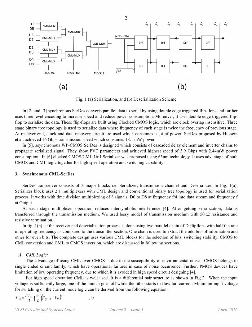
Fig. 1 (a) Serialization, and (b) Deserialization Scheme
In [2] and [3] synchronous SerDes converts parallel data to serial by using double edge triggered flip-flops and further
uses three level encoding to increase speed and reduce power consumption. Moreover, it uses double edge triggered flip-flop to serialize the data. These flip-flops are built using Clocked CMOS logic, which are clock overlap insensitive. Three stage binary tree topology is used to serialize data where frequency of each stage is twice the frequency of previous stage. At receiver end, clock and data recovery circuit are used which consumes a lot of power. SerDes proposed by Hussein et.al. achieved 16 Gbps transmission speed which consumes 18.1 mW power.
In [5], asynchronous WP-CMOS SerDes is designed which consists of cascaded delay element and inverter chains to propagate serialized signal. They show PVT parameters and achieved highest speed of 3.9 Gbps with 2.44mW power consumption. In [6] clocked CMOS/CML 16:1 Serializer was proposed using 65nm technology. It uses advantage of both CMOS and CML logic together for high speed operation and switching capability.
3. Synchronous CML-SerDes
SerDes transceiver consists of 3 major blocks i.e. Serializer, transmission channel and Deserializer. In Fig. 1(a),
Serializer block uses 2:1 multiplexers with CML design and conventional binary tree topology is used for serialization process. It works with time division multiplexing of 8 signals, D0 to D8 at frequency f/4 into data stream and frequency f at Output.
At each stage multiplexer operation reduces intersymbolic interference [4]. After getting serialization, data is transferred through the transmission medium. We used lossy model of transmission medium with 50 Ω resistance and resistive termination.
In fig. 1(b), at the receiver end deserialization process is done using two parallel chain of D-flipflops with half the rate of operating frequency as compared to the transmitter section. One chain is used to extract the odd bits of information and other for even bits. The complete design uses various CML blocks for the selection of bits, switching stability, CMOS to CML conversion and CML to CMOS inversion, which are discussed in following sections.
A. CML Logic:
The advantage of using CML over CMOS is due to the susceptibility of environmental noises. CMOS belongs to single ended circuit family, which have operational failures in case of noise occurrence. Further, PMOS devices have limitation of low operating frequency, due to which it is avoided in high speed circuit designing [4].
For high speed operation CML is well used. It is a differential pair structure as shown in Fig 2. When the input voltage is sufficiently large, one of the branch goes off while the other starts to flow tail current. Minimum input voltage for switching on the current mode logic can be derived from the following equation.
( )22,12,1 2 thgsox VV
LWC
I −⎟⎠
⎞⎜⎝
⎛=µ (1)
(a)(b)

4
VLSI Circuits and Systems Letter Volume 2 – Issue 1 April 2016
021 III =+ (2)
21 gsgsin VVV −= (3) After solving the above equation, the minimum voltage to turn on the transistor with current equal to the current source
is:
)/(2 0
(min) LWCIV
oxin µ
= (4)
The voltage swing is: 00)()0( RIIiViVV ==−==Δ (5)
Voltage swing of the CML logic is the product of resistive load and the tail current. So the speed of circuit can be
improved by decreasing the voltage swing. It will also help in reducing noise margin, but excessive reduction results in switching between next differential pair.
B. 2:1 CML MULTIPLEXER: 2:1 CML Multiplexer is shown in Fig 3, in which two resistive loaded parallel differential pairs are used with
selection switch control [4]. The selection switch defines which input should be selected at any instance, and transfer it to the output. If the selection bit Sp is high, then the input A is selected and if Sp is low then input B is selected to pass the tail current. Input bits are first converted from the CMOS logic to CML by using CML logic for processing in the multiplexer.
C. CML Latch CML latch [6] is a little bit different from the multiplexer, in latch the second input B is connect to outputs as shown in
Fig. 4. Due to that change, it shows stable output in case of low latch signal. Input and output for the synchronous CML is the CMOS logics. For designing the transceiver, the CMOS to CML converters used at input side and for the output CML to CMOS converter as implemented in by Tondo et.al. [6]
Input and output for the synchronous CML is the CMOS logics. For designing the transceiver, the CMOS to CML converters used at input side and for the output CML to CMOS converter as implemented in by Tondo et.al. [6]
Fig. 2 CML Logic

5
VLSI Circuits and Systems Letter Volume 2 – Issue 1 April 2016
Fig. 3 CML Mux Design
Fig. 4 CML Latch
4. Simulation Results
In this section, simulation results for synchronous CML SerDes are discussed. Proposed synchronous CML SerDes is
designed using UMC 65nm technology. Clock circuitry is used to generate multiple clock signals at Serializer and Deserializer. It helped in easy recovery of parallel digital output signal at receiver end.
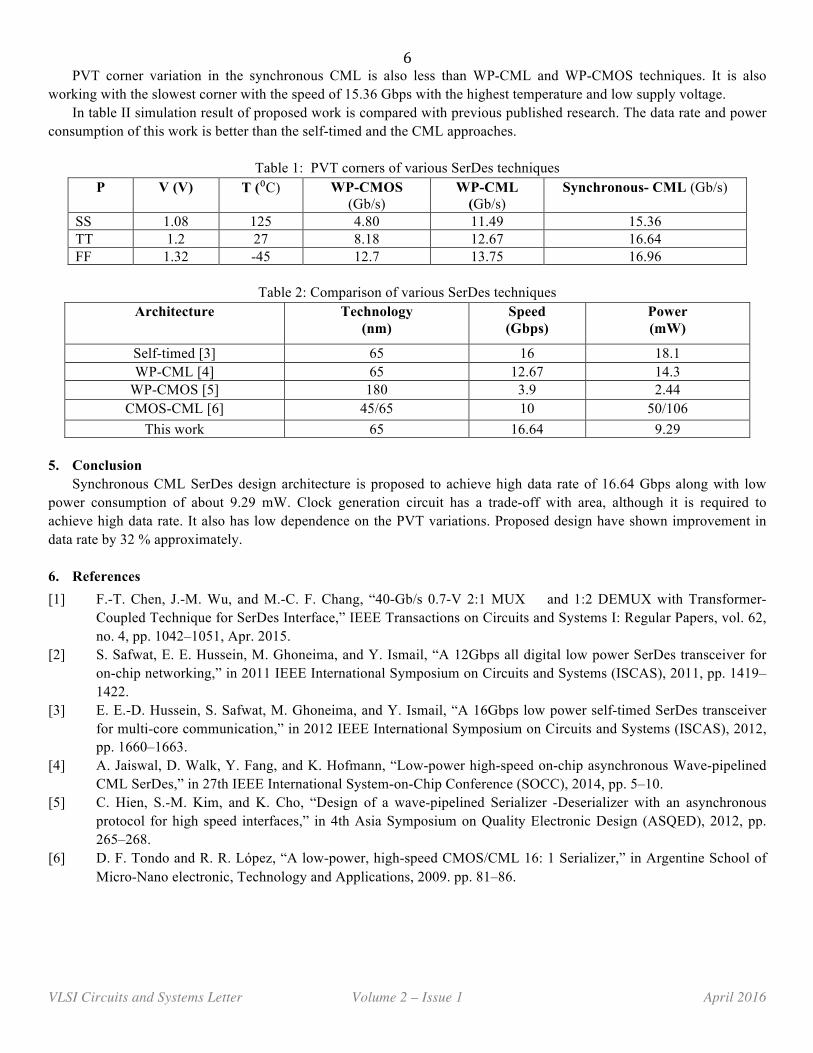
PVT corner variations are evaluated for the stable outputs PVT simulation is shown in table I which compares proposed design with WP-CMOS and WP-CML. Synchronous CML design operates with data rate of 16.64Gbps.
R R
R R
6
VLSI Circuits and Systems Letter Volume 2 – Issue 1 April 2016
PVT corner variation in the synchronous CML is also less than WP-CML and WP-CMOS techniques. It is also working with the slowest corner with the speed of 15.36 Gbps with the highest temperature and low supply voltage.
In table II simulation result of proposed work is compared with previous published research. The data rate and power consumption of this work is better than the self-timed and the CML approaches.
Table 1: PVT corners of various SerDes techniques
P V (V) T (⁰C) WP-CMOS (Gb/s)
WP-CML (Gb/s)
Synchronous- CML (Gb/s)
SS 1.08 125 4.80 11.49 15.36 TT 1.2 27 8.18 12.67 16.64 FF 1.32 -45 12.7 13.75 16.96
Table 2: Comparison of various SerDes techniques
Architecture Technology (nm)
Speed (Gbps)
Power (mW)
Self-timed [3] 65 16 18.1 WP-CML [4] 65 12.67 14.3
WP-CMOS [5] 180 3.9 2.44 CMOS-CML [6] 45/65 10 50/106
This work 65 16.64 9.29
5. Conclusion Synchronous CML SerDes design architecture is proposed to achieve high data rate of 16.64 Gbps along with low
power consumption of about 9.29 mW. Clock generation circuit has a trade-off with area, although it is required to achieve high data rate. It also has low dependence on the PVT variations. Proposed design have shown improvement in data rate by 32 % approximately.
6. References [1] F.-T. Chen, J.-M. Wu, and M.-C. F. Chang, “40-Gb/s 0.7-V 2:1 MUX and 1:2 DEMUX with Transformer-
Coupled Technique for SerDes Interface,” IEEE Transactions on Circuits and Systems I: Regular Papers, vol. 62, no. 4, pp. 1042–1051, Apr. 2015.
[2] S. Safwat, E. E. Hussein, M. Ghoneima, and Y. Ismail, “A 12Gbps all digital low power SerDes transceiver for on-chip networking,” in 2011 IEEE International Symposium on Circuits and Systems (ISCAS), 2011, pp. 1419–1422.
[3] E. E.-D. Hussein, S. Safwat, M. Ghoneima, and Y. Ismail, “A 16Gbps low power self-timed SerDes transceiver for multi-core communication,” in 2012 IEEE International Symposium on Circuits and Systems (ISCAS), 2012, pp. 1660–1663.
[4] A. Jaiswal, D. Walk, Y. Fang, and K. Hofmann, “Low-power high-speed on-chip asynchronous Wave-pipelined CML SerDes,” in 27th IEEE International System-on-Chip Conference (SOCC), 2014, pp. 5–10.
[5] C. Hien, S.-M. Kim, and K. Cho, “Design of a wave-pipelined Serializer -Deserializer with an asynchronous protocol for high speed interfaces,” in 4th Asia Symposium on Quality Electronic Design (ASQED), 2012, pp. 265–268.
[6] D. F. Tondo and R. R. López, “A low-power, high-speed CMOS/CML 16: 1 Serializer,” in Argentine School of Micro-Nano electronic, Technology and Applications, 2009. pp. 81–86.
7
VLSI Circuits and Systems Letter Volume 2 – Issue 1 April 2016
Review on Post Silicon Validation of Physical Unclonable Functions Sudeendra Kumar K, Sauvagya Sahoo, K. K. Mahapatra National Institute of Technology, Rourkela Abstract – Globalization of semiconductor design and manufacturing has raised several security issues like counterfeit parts, IP protection and hardware Trojans. At the same time, growth of semiconductor industry is driven by Internet of things (IoT’s), in which security is of prime importance. In this juncture, a hardware security primitive: Physical Unclonable Function (PUF) can be a promising solution to solve the security issues related to IoT and hardware security. The various PUF circuits are proposed by researchers in last few years. Post silicon validation of PUF is very important to understand the PUF characteristics. Based on the characterization results, suitable measures can address the future problems related to aging, fault attacks etc at deployment. In this letter, we briefly present the literature review of post silicon validation of PUF and conclude by listing out the possible topics for future research.
1. Introduction Internet of Things (IoT’s) is active network of smart physical objects are getting mainstream. Applications of IoT’s can be found in various fields like home automation, industrial control, smart cities etc. The smart IoT devices connect automatically to each other and exchange private and sensitive data. There is a need to develop techniques to ensure the security in the IoT operations. IoT’s are generally battery operated devices with limited computational capabilities. Software Implementations of cryptographic algorithms are vulnerable to attacks. It is a challenge to design a low power, computationally efficient and low memory foot print cryptographic algorithms for IoT’s. In this juncture, physical unclonable function (PUF) comes handy to address the issues related to security in IoT’s [1]. PUF is a hardware security primitive, which has got applications in cryptographic key generation, anti-counterfeiting etc. It is always better if the root of trust comes from hardware and it is best fit in the IoT’s security space. Researchers at MIT proposed PUFs decade ago, which is suitable for various security applications [2]. The inherent process variations in silicon manufacturing create PUF in each IC, which acts like a DNA of that particular IC. PUF is a partially disordered physical function will have a unique response for each input (challenge). The large numbers of challenge response (input-output) pairs (CRP’s) are unique for given IC and useful in identification and authentication of IC. The wide variety of PUF circuits are proposed by researchers targeting both ASIC and FPGA [3]. The features of PUF like uniqueness, reliability and uniformity decide the quality of PUF circuits.
By incorporating the PUF circuit in chips, it is easy to build various security applications like device authentication, cryptographic key generation etc. After fabrication of devices, the mandatory requirement for chip design house is to collect the challenge-response pairs (CRP’s) of each IC manufactured and store them in a secure server. The CRP data is analysed for security metrics like uniqueness, reliability and uniformity offline. The widely accepted offline analysis considers CRP data from all the chips fabricated. Evaluation, testing and characterization of PUF circuit is an unexplored research area. A comprehensive test methodology is required for post silicon validation of PUF, which should address following issues:-
• Cost effective techniques to evaluate the PUF on each individual IC during ATE testing (Production testing). • Characterization of PUF metrics across voltage and temperatures. • In-field testing and validation of PUF circuit to assess the effect of temperature and other environmental
conditions on CRP, aging effects etc. • On-chip monitoring, activation and de-activation of compensation circuits to sustain the reliability of CRP’s
against environmental conditions and aging. • On-chip monitors to assess the attacks and activation of countermeasure circuits to defend the attacks.
8
VLSI Circuits and Systems Letter Volume 2 – Issue 1 April 2016
In this letter, we review the published literature in connection with post silicon validation of PUF for the above mentioned issues and conclude by stating the open problems.
2. Introduction
Internet of Things (IoT’s) is active network of smart physical objects are getting mainstream. Applications of IoT’s can be found in various fields like home automation, industrial control, smart cities etc. The smart IoT devices connect automatically to each other and exchange private and sensitive data. There is a need to develop techniques to ensure the security in the IoT operations. IoT’s are generally battery operated devices with limited computational capabilities. Software Implementations of cryptographic algorithms are vulnerable to attacks. It is a challenge to design a low power, computationally efficient and low memory foot print cryptographic algorithms for IoT’s. In this juncture, physical unclonable function (PUF) comes handy to address the issues related to security in IoT’s [1]. PUF is a hardware security primitive, which has got applications in cryptographic key generation, anti-counterfeiting etc. It is always better if the root of trust comes from hardware and it is best fit in the IoT’s security space. Researchers at MIT proposed PUFs decade ago, which is suitable for various security applications [2]. The inherent process variations in silicon manufacturing create PUF in each IC, which acts like a DNA of that particular IC. PUF is a partially disordered physical function will have a unique response for each input (challenge). The large numbers of challenge response (input-output) pairs (CRP’s) are unique for given IC and useful in identification and authentication of IC. The wide variety of PUF circuits are proposed by researchers targeting both ASIC and FPGA [3]. The features of PUF like uniqueness, reliability and uniformity decide the quality of PUF circuits.
By incorporating the PUF circuit in chips, it is easy to build various security applications like device authentication, cryptographic key generation etc. After fabrication of devices, the mandatory requirement for chip design house is to collect the challenge-response pairs (CRP’s) of each IC manufactured and store them in a secure server. The CRP data is analysed for security metrics like uniqueness, reliability and uniformity offline. The widely accepted offline analysis considers CRP data from all the chips fabricated. Evaluation, testing and characterization of PUF circuit is an unexplored research area. A comprehensive test methodology is required for post silicon validation of PUF, which should address following issues:-
• Cost effective techniques to evaluate the PUF on each individual IC during ATE testing (Production testing). • Characterization of PUF metrics across voltage and temperatures. • In-field testing and validation of PUF circuit to assess the effect of temperature and other environmental
conditions on CRP, aging effects etc. • On-chip monitoring, activation and de-activation of compensation circuits to sustain the reliability of CRP’s
against environmental conditions and aging. • On-chip monitors to assess the attacks and activation of countermeasure circuits to defend the attacks.
In this letter, we review the published literature in connection with post silicon validation of PUF for the above mentioned issues and conclude by stating the open problems.
3. Prior work
To date, there are very few papers published related to post silicon validation of PUF. Most of the previous work is based on software-evaluations on collected CRP data. Testing the security features of PUF is explained in [4] for the first time. Apart from the general security metrics like uniqueness, reliability and uniformity this work proposes several other tests like predictability test, collision test, sensitivity test and reverse engineering test to evaluate the security properties of PUFs. All the tests are performed offline on the collected CRPs.
9
VLSI Circuits and Systems Letter Volume 2 – Issue 1 April 2016
Post silicon validation of PUF and True Random Number Generators (TRNG) based on reliability monitors is proposed in [5]. Reliability monitor based on time to digital converter (TDC) is deployed on-chip to measure delay between two identical paths. Reliability monitor generates 2-bit response based on the instantaneous time difference. Based on the output of reliability monitor, decision on reliability of particular challenge-response pair can be taken. If CRP is not reliable, then that particular pair can be dropped and it will be not used in any application.
Another significant work from Hussain and others is to design a BIST for post silicon validation of PUF [6]. This work presents on the fly evaluation of PUFs and TRNGs. The BIST structure is designed to evaluate the two important properties of PUF: unpredictability and stability. As the authors claim, this work is first BIST scheme for on the fly assessment of PUFs to perform quantitative online analysis. The proposed BIST scheme is validated on FPGA. Comparison of all the three papers is shown in Table.1.
4. Conclusion and Future wok The three significant papers in connection with post silicon validation of PUFs are briefly discussed. Post silicon validation of PUF is an important research area which is still unexplored. Development of suitable post silicon techniques for PUFs will make the industry job easy to bring the PUF circuits in their mainstream products and applications. Based on this review, we can predict the future work in post silicon validation of PUF will focus on:-
• Development of on-chip structures for better characterization of PUF on ATE in cost effective way. • Development of on-chip structures for online monitoring, analysis and defence against environmental effects,
aging, and fault attacks. 5. References [1] D.Miorandi, S.Sicari, F.D. Pellegrini and I. Chlamtac, “Internet of things: Vision, applications and research
challenges”, Ad Hoc Networks, 2012. [2] B.Gassend, D.Clarke, M. Van Dijk, S. Devdas, “Silicon physical random functions”, in ACM conf. on computer and
communications security, 2002. [3] Charles herder, Meng-day Yu, F.Koushanfar, S. Devadas, “Physical Unclonable Functions and Applications: A
Tutorial”, Proceedings of the IEEE, Vol.102, No.8, August-2014. [4] M.Majzoobi, F.Koushanfar and M.Potkonjak, “Testing techniques for hardware security”, in IEEE International Test
Conf. 2008, pp, 1-10. [5] Xiaolin Xu, Vikram Suresh, Raghavan kumar, Wayne Burleson, “Post-silicon validation and calibration of Hardware
Security Primitives”, in IEEE Computer Society Annual Symposium on VLSI-2014. [6] Siam Hussain, Mehrdad Majzoobi, Farinaz Koushanfar, "A Built-In-Self-Test Scheme for Online Evaluation of
Physical Unclonable Functions and True Random Number Generators", IEEE Transactions on Multi-Scale Computing Systems , 2016.
Architecture-Centric Integration Challenges for Automotive Cyber-Physical Systems HuafengYu Toyota Info Technology Center Next generation automotive systems, including new advanced driver assistance systems and autonomous vehicles, have plenty of new electronic devices, like radar and LIDAR sensors, multicore processors, GPUs and FPGAs. They also have new functionalities, such as machine learning algorithms, as well as security and connectivity. As a result, the complexity of the systems has been dramatically increased and its design is becoming extremely challenging. Particularly the conventional development approaches, processes and tools are not well adapted to new design requirements on safety, reliability, performance, security, cost, etc.
10
VLSI Circuits and Systems Letter Volume 2 – Issue 1 April 2016
We first present several design challenges in the automotive domain. The automotive system development is generally based on informal requirements, provided by car manufacturers (Original Equipment Manufacturer - OEMs) to suppliers. But the requirements may lead to misunderstanding because of its ambiguity in semantics. Moreover, subsystems, electronics and software components are increasingly developed by different suppliers in a separated and parallel manner. And the final integration [1], performed by OEMs, is always difficult due to the compatibility of the subsystems and components. The timing issue is among the most significant concerns in automotive system design. It is not only from the delays and deadlines, but also synchronization and causality. In general, the timing issue becomes more explicit when Electrical/Electronic architecture is considered and the system is integrated. Recent reports on security-related vehicle hacking involve various systems in many models from different OEM’s. A series of successful hacking activities of current car models show the lack of system-level security consideration in vehicle hardware and software design, integration, certification, and production. These concerns also rise to US political level [2]. Integration of security mechanisms in vehicles involves computing resources as well as other aspects, like safety, reliability, cost. The overall safety of next-generation automotive systems is not only based on the reliability of mechanics and electronics, but also the correctness of the software controllers and security of the vehicles. It also requires high computing capability as well as less power consumption, as a result of increased number of functionalities and devices integrated into the system. Current automotive electronics architecture can hardly provide that capability, which eventually needs the great support from both EDA and VLSI communities. One of the recent solutions to address previous challenges is model-based systems design, where various general or domain-specific modeling languages are adopted, such as SysML, MATLAB/Simulink, SCADE and Modelica, in order to meet different design needs, including different application domains, performance, expertise, cost, etc. But there is still a problem of model integration due to the semantic dissimilarity between models and their inherent formalism [3]. From the integration point of view, we also need to consider automotive architecture, which is rarely formalized in conventional automotive design processes and generally leads to a manual, error-prone, time-consuming architecture exploration and validation. To avoid this problem, formalization, formal reasoning, and early-phase exploration are required, along with explicit quality attributes associated with particular architectural entities. Architecture description languages, such as AADL [4], AUTOSAR and EAST-ADL, haven been therefore proposed and standardized for cyber-physical systems, especially in aviation and automotive systems. We propose a system-level design and integration framework [5], dedicated to automotive model-based systems engineering, via an architecture-centric design approach. In this framework, software architecture is explicitly specified with AADL. From a view-based design approach, behavioral, architectural, and timing views of the system are all considered, along with the compositional view of system models. Multiple formalism and languages are adopted for each view [6], for example, Simulink for behavioral view, AADL for architectural view, contract for compositional view, and synchronous languages for timing view. Formal evaluation of the system is first performed on each view in a separated way, and then in an integrated way in our proposed integration framework. This framework has been developed to support a model-based system-level co-design and integration of automotive systems.
1. Reference [1] E. Markey. Tracking & hacking: Security & privacy gaps put American drivers at risk, 2015. [2] E.A. Lee, et al. A Framework for Comparing Models of Computation. IEEE Transactions on Computer-Aided Design
of Integrated Circuits and Systems, 17(12):1217-1229, 2006. [3] Society of Automotive Engineers. Aerospace Standard AS5506A: Architecture Analysis and Design Language
(AADL). SAE AS5506A, 2009.
11
VLSI Circuits and Systems Letter Volume 2 – Issue 1 April 2016
[4] H. Yu, et al. The challenge of interoperability: model-based integration for automotive control software, In DAC, 58:1-58:6, 2015.
[5] Y. Ma, et al. Toward Polychronous Analysis and Validation for Timed Software Architectures in AADL. In DATE, pages 1173-1178, 2013.
[6] M. Broy. Challenges in Automotive Software Engineering. In International Conference on Software Engineering (ICSE), 2006.
Physical Design for 3D Integrated Circuits ISBN: 978-1-4987-1036-7 Editors: Aida Todri-Sanial and Chuan Seng Tan https://www.crcpress.com/Physical-Design-for-3D-Integrated-Circuits/TodriSanial-Tan/9781498710367
This book reveals how to effectively and optimally design 3D integrated circuits (ICs). It also analyzes the design tools for 3D circuits while exploiting the benefits of 3D technology. The book begins by offering an overview of physical design challenges with respect to conventional 2D circuits, and then each chapter delivers an in-depth look at a specific physical design topic. Featuring contributions from renowned experts in their respective fields, this comprehensive reference provides a single, convenient source of cutting-edge information for those pursuing 2.5D/3D technology. Chapter 1: Overview of 3D Technology by Chuan Seng Tan Chapter 2: Physical Design Issues Overview by Aida Todri-Sanial Chapter 3: Detailed Electrical and Reliability Study of Tapered TSV by Tiantao Lu and Ankur Srivastava Chapter 4: 3D Interconnect Extraction by Sung Kyu Lim Chapter 5: 3D Placement & Routing by Pingqiang Zhou and Sachin Sapatnekar Chapter 6: Power and Signal Integrity Challenges in 3D System-on-Chip by Emre Salman Chapter 7: Design Methodology for 3D Clock Networks by Taewhan Kim and Heechun Park
12
VLSI Circuits and Systems Letter Volume 2 – Issue 1 April 2016
Chapter 8: Design Methodology for 3D Power Delivery Networks by Aida Todri-Sanial Chapter 9: Live Free or Die Hard: Design for Reliability in Three-Dimensional Integrated Circuits by Yu-Guang Chen, Yiyu Shi, and Shih-Chieh Chang Chapter 10: Thermal Modeling and Management for 3D-Stacked Systems by Tiansheng Zhang, Fulya Kaplan and Ayse K. Coskun Chapter 11: Thermal Management of 3D Systems-on-Chip by Sumeet S. Kumar, Amir Zjajo and Rene Van Leuken Chapter 12: Dynamic Thermal Optimization for 3D Many-Core Systems by Nizar Dahir, Ra’ed Al-Dujaily, Terrence Mak and Alex Yakolev Chapter 13: Parasitic coupling analysis in 3D circuits by Brad Gaynor, Nauman Khan and Soha Hassoun Chapter 14: Overview of 3D CAD Design Tools by Andy Heinig and Robert Fischbach Chapter 15: Design challenges and solutions for Monolithic 3D ICs by Sung Kyu Lim and Yiyu Shi Chapter 16: Design of High Speed Interconnects for 3D/2.5D ICs without TSVs by Tony Tae-Hyoung Kim Chapter 17: Challenges and Future Directions of 3D Physical Design by Johann Knechtel, Jens Lienig and Cliff C. N. Sze
Opinions
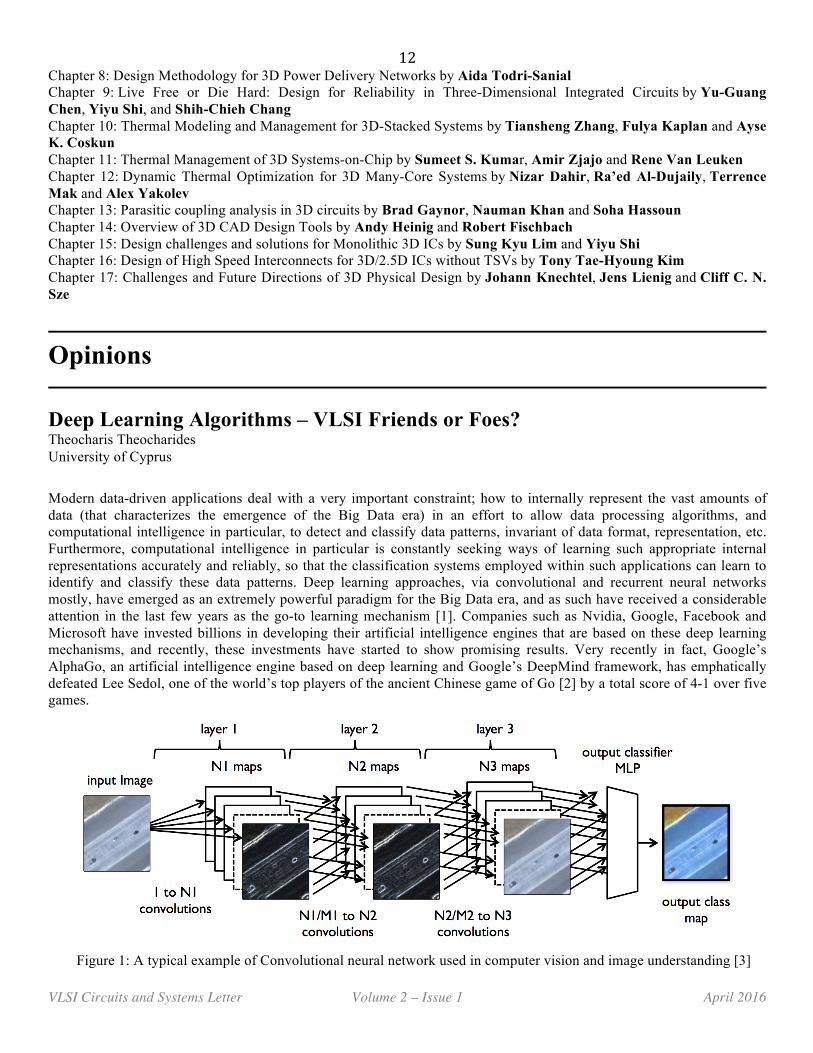
Deep Learning Algorithms – VLSI Friends or Foes? Theocharis Theocharides University of Cyprus Modern data-driven applications deal with a very important constraint; how to internally represent the vast amounts of data (that characterizes the emergence of the Big Data era) in an effort to allow data processing algorithms, and computational intelligence in particular, to detect and classify data patterns, invariant of data format, representation, etc. Furthermore, computational intelligence in particular is constantly seeking ways of learning such appropriate internal representations accurately and reliably, so that the classification systems employed within such applications can learn to identify and classify these data patterns. Deep learning approaches, via convolutional and recurrent neural networks mostly, have emerged as an extremely powerful paradigm for the Big Data era, and as such have received a considerable attention in the last few years as the go-to learning mechanism [1]. Companies such as Nvidia, Google, Facebook and Microsoft have invested billions in developing their artificial intelligence engines that are based on these deep learning mechanisms, and recently, these investments have started to show promising results. Very recently in fact, Google’s AlphaGo, an artificial intelligence engine based on deep learning and Google’s DeepMind framework, has emphatically defeated Lee Sedol, one of the world’s top players of the ancient Chinese game of Go [2] by a total score of 4-1 over five games.
Figure 1: A typical example of Convolutional neural network used in computer vision and image understanding [3]
13
VLSI Circuits and Systems Letter Volume 2 – Issue 1 April 2016
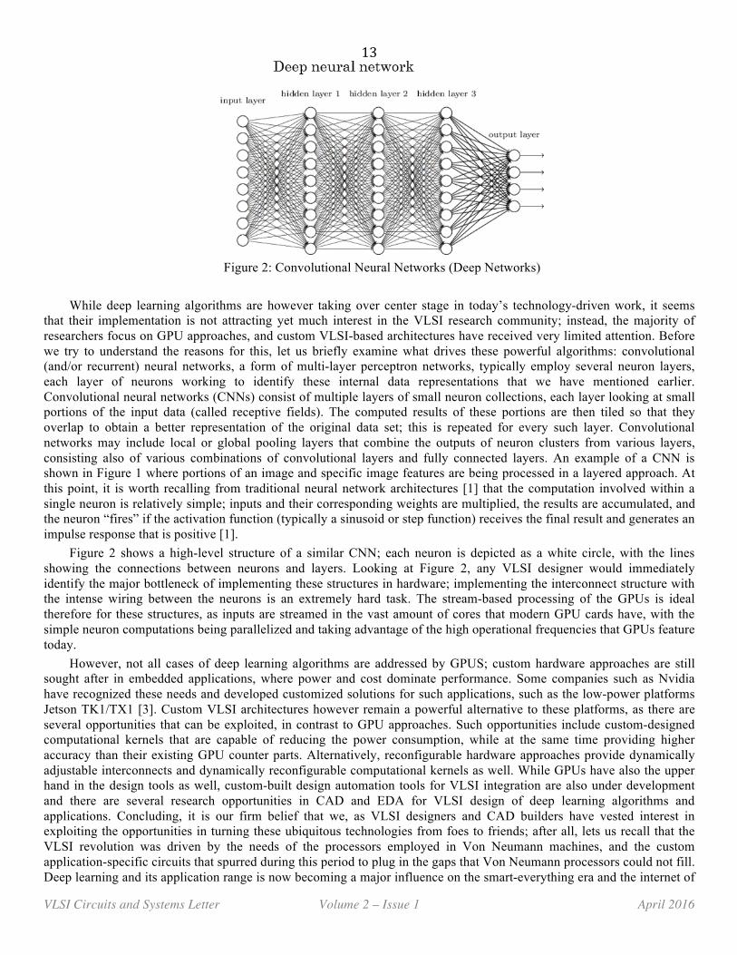
Figure 2: Convolutional Neural Networks (Deep Networks)
While deep learning algorithms are however taking over center stage in today’s technology-driven work, it seems
that their implementation is not attracting yet much interest in the VLSI research community; instead, the majority of researchers focus on GPU approaches, and custom VLSI-based architectures have received very limited attention. Before we try to understand the reasons for this, let us briefly examine what drives these powerful algorithms: convolutional (and/or recurrent) neural networks, a form of multi-layer perceptron networks, typically employ several neuron layers, each layer of neurons working to identify these internal data representations that we have mentioned earlier. Convolutional neural networks (CNNs) consist of multiple layers of small neuron collections, each layer looking at small portions of the input data (called receptive fields). The computed results of these portions are then tiled so that they overlap to obtain a better representation of the original data set; this is repeated for every such layer. Convolutional networks may include local or global pooling layers that combine the outputs of neuron clusters from various layers, consisting also of various combinations of convolutional layers and fully connected layers. An example of a CNN is shown in Figure 1 where portions of an image and specific image features are being processed in a layered approach. At this point, it is worth recalling from traditional neural network architectures [1] that the computation involved within a single neuron is relatively simple; inputs and their corresponding weights are multiplied, the results are accumulated, and the neuron “fires” if the activation function (typically a sinusoid or step function) receives the final result and generates an impulse response that is positive [1].
Figure 2 shows a high-level structure of a similar CNN; each neuron is depicted as a white circle, with the lines showing the connections between neurons and layers. Looking at Figure 2, any VLSI designer would immediately identify the major bottleneck of implementing these structures in hardware; implementing the interconnect structure with the intense wiring between the neurons is an extremely hard task. The stream-based processing of the GPUs is ideal therefore for these structures, as inputs are streamed in the vast amount of cores that modern GPU cards have, with the simple neuron computations being parallelized and taking advantage of the high operational frequencies that GPUs feature today.
However, not all cases of deep learning algorithms are addressed by GPUS; custom hardware approaches are still sought after in embedded applications, where power and cost dominate performance. Some companies such as Nvidia have recognized these needs and developed customized solutions for such applications, such as the low-power platforms Jetson TK1/TX1 [3]. Custom VLSI architectures however remain a powerful alternative to these platforms, as there are several opportunities that can be exploited, in contrast to GPU approaches. Such opportunities include custom-designed computational kernels that are capable of reducing the power consumption, while at the same time providing higher accuracy than their existing GPU counter parts. Alternatively, reconfigurable hardware approaches provide dynamically adjustable interconnects and dynamically reconfigurable computational kernels as well. While GPUs have also the upper hand in the design tools as well, custom-built design automation tools for VLSI integration are also under development and there are several research opportunities in CAD and EDA for VLSI design of deep learning algorithms and applications. Concluding, it is our firm belief that we, as VLSI designers and CAD builders have vested interest in exploiting the opportunities in turning these ubiquitous technologies from foes to friends; after all, lets us recall that the VLSI revolution was driven by the needs of the processors employed in Von Neumann machines, and the custom application-specific circuits that spurred during this period to plug in the gaps that Von Neumann processors could not fill. Deep learning and its application range is now becoming a major influence on the smart-everything era and the internet of
14
VLSI Circuits and Systems Letter Volume 2 – Issue 1 April 2016
things, which are expected to be one of the dominant markets of the next decade. While GPUs therefore maybe a preferred platform for such applications currently, custom VLSI circuits will always however be needed to cover the gaps that GPUS cannot fill; as the application range becomes more focused, these gaps will become more significant. References [1] Yann LeCun, Yoshua Bengio and Geoffrey Hinton, “Deep learning”, Nature. No. 521. 2015, pp. 436–444. DOI: 10.1038/nature14539 [2] http://www.wired.com/2016/03/googles-ai-wins-fifth-final-game-go-genius-lee-sedol/ , online, accessed March 2016 [3] Purdue’s e-Lab (e-lab.github.io/html/research-intelligent-vision-systems.html) – Online, Accessed March 2016 [4] https://developer.nvidia.com/embedded-computing, online, accessed March 2016.
Bringing out a Natural Computer (Ribosome) from within a Cell: A Next-Gen Alternative? Prasun Ghosal, Pratima Chatterjee and Mayukh Sarkar Indian Institute of Engineering Science and Technology, Shibpur, India What is a cell? A cell is generally the basic unit of any living organism. It is membrane-bounded and consists of protoplasm, which is self reproductive in nature and structural, functional unit of a life [2]. It contains the genetic information in the form of a DNA (Deoxyribo Nucleic Acid) inside the chromosome (in case of an eukaryotic cell) or in genetic material (in case of a prokaryotic cell). Some cell has several membrane-bounded and membrane-less organelles in which several biomolecular operations are performed [2]. Ribosome is one of them. What is Ribosome? In a cell, ribosome is the most common organelle and can be found in all types of cells. Abundant numbers of ribosomes are present in a cell. It acts as a translator in a cell. It translates the genetic code into the sequence of amino acids. This procedure is termed as translation or in general, protein synthesis. Structure of a Ribosome Ribosome is tiny in size having the diameter of only 20-30nm. It consists of two sub-units, viz. one smaller and the other one larger. Two types of ribosome are found as per the type of sub-units, i.e. 80S ribosome (in case of eukaryotes) and 70S ribosome (in case of prokaryotes), where, S is the Svedberg's unit used to measure the sedimentation characteristics. The sub-units are composed of ribozyme and proteins. Ribozymes are special type of RNA (Ribo Nucleic Acid) having catalytic property i.e. it can control the bimolecular reactions. Ribozyme is also known as rRNA or ribosomal RNA. In case of eukaryotic cell, larger sub-unit is of 60S type and smaller sub-unit is of 40S type. The upper sub-unit consists of 5S, 28S, 5.8S types of rRNA and 46 proteins, and the lower sub-unit consists of 18S rRNA and 33 proteins. In prokaryotic cell, the larger sub-unit is of 50S type and the smaller one is of 30S type. The upper sub-unit consists of 5S and 23S rRNA and 31 proteins. On the other hand, lower sub-unit consists of 16S rRNA and 21 proteins. Ribosome has three sites, viz., A site, P site, and E site. These are called mRNA binding sites in a ribosome. These sites help in protein

15
VLSI Circuits and Systems Letter Volume 2 – Issue 1 April 2016
synthesis. A site is present in ribosome at the entrance of the mRNA. P site is situated just beside A site and at the middle of A site and E site. E site is present at the last region of the tunnel through which the mRNA is passed. Another tunnel is present in a ribosome through which nascent peptide chain is passed. This tunnel stays beside the PTC (Peptidyl transferase recreation centre). The structure of a ribosome is shown in Figure 1.
Figure 1: The structure of a ribosome.
How the protein is synthesized in a ribosome? DNA is the main information carrier. DNA produces mRNA and this mRNA carries the instruction for synthesizing a protein molecule. The procedure to create mRNA from DNA is termed as transcription. Protein synthesis or translation process occurs in ribosome. Protein synthesis is a process by which a cell synthesizes a polypeptide chain by translating mRNA codon that is transcribed from the DNA or genetic informer body. This entire procedure of transcription in which the genetic code is just transferred into mRNA and translation in which the genetic information is translated into amino acid sequence is collectively known as central dogma. So, mRNA plays a major role in protein synthesis procedure. It is also called reporter RNA. The mRNA is bounded to the smaller sub-unit by the Shine-Dalgarno Sequence. Shine-Dalgarno sequence is a specific identifying gene sequence that is present in the mRNA and its corresponding Anti Shine-Dalgarno sequence is present in ribozyme (rRNA) of smaller sub-unit of the ribosome. In protein synthesis [3] another type of RNA, known as tRNA (Transfer RNA) also plays a major role. These are created from nucleus and act as a mediator between amino acids and polypeptide chain. It binds amino acid to its binding site and has a complementary base pair for each triplet codon of mRNA. Aminoacyle-synthetase helps in binding the amino acid to tRNA. At the time of initiation of protein synthesis, proper mRNA is attached to its corresponding subunit with the help of Shine-Dalgarno sequence. Next, upper sub-unit is attached to this complex to build the complete system. At each triplet codon of mRNA upper sub-unit brings Aminoacyle-tRNA to its A site using mRNA template. PTC (Peptidyl Transferase Centre) extracts peptidyl-tranferase enzyme by which newly brought amino acid is attached to peptide chain of P site. This procedure of attachment of amino acid to the nascent peptide chain is termed as protein chain elongation. Then mRNA shifts by a triplet codon and the codon under A site comes under P site and new triplet codon comes under A site. The tRNA also moves from A site to P site with the codon. Each specific triplet codon is responsible for an amino acid and also for the start and end of translation. AUG codon is referred to as start codon and UAG, UUA, and UGA are the end codons. AUG is also responsible for methionine amino acid. So, at the beginning of each nascent protein chain must contain the methionine but it may be discarded later. An overview of the protein synthesis procedure is shown in Figure 2.
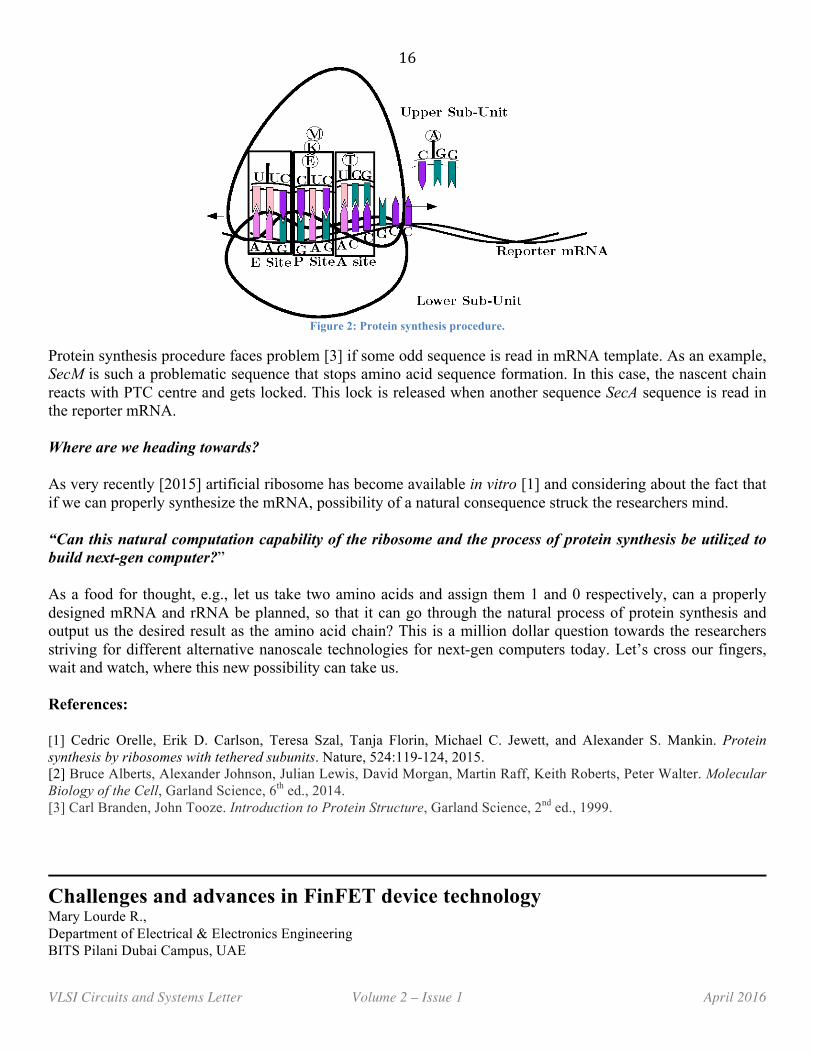
16
VLSI Circuits and Systems Letter Volume 2 – Issue 1 April 2016
Figure 2: Protein synthesis procedure.
Protein synthesis procedure faces problem [3] if some odd sequence is read in mRNA template. As an example, SecM is such a problematic sequence that stops amino acid sequence formation. In this case, the nascent chain reacts with PTC centre and gets locked. This lock is released when another sequence SecA sequence is read in the reporter mRNA. Where are we heading towards? As very recently [2015] artificial ribosome has become available in vitro [1] and considering about the fact that if we can properly synthesize the mRNA, possibility of a natural consequence struck the researchers mind.
“Can this natural computation capability of the ribosome and the process of protein synthesis be utilized to build next-gen computer?”
As a food for thought, e.g., let us take two amino acids and assign them 1 and 0 respectively, can a properly designed mRNA and rRNA be planned, so that it can go through the natural process of protein synthesis and output us the desired result as the amino acid chain? This is a million dollar question towards the researchers striving for different alternative nanoscale technologies for next-gen computers today. Let’s cross our fingers, wait and watch, where this new possibility can take us. References: [1] Cedric Orelle, Erik D. Carlson, Teresa Szal, Tanja Florin, Michael C. Jewett, and Alexander S. Mankin. Protein synthesis by ribosomes with tethered subunits. Nature, 524:119-124, 2015. [2] Bruce Alberts, Alexander Johnson, Julian Lewis, David Morgan, Martin Raff, Keith Roberts, Peter Walter. Molecular Biology of the Cell, Garland Science, 6th ed., 2014. [3] Carl Branden, John Tooze. Introduction to Protein Structure, Garland Science, 2nd ed., 1999.
Challenges and advances in FinFET device technology Mary Lourde R., Department of Electrical & Electronics Engineering BITS Pilani Dubai Campus, UAE
17
VLSI Circuits and Systems Letter Volume 2 – Issue 1 April 2016
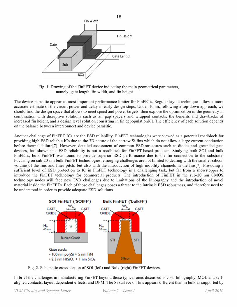
Introduction The development of the MOSFET scale length theory from the 1970s to the present, has evolved from the one-region model for bulk MOSFETs, to the two-region model for dealing with thick, high-k gate dielectrics, then to the three-region model for multiple-gate MOSFETs such as FinFETs. Technology evolution brings new challenges to integrated circuits (IC) design. For any given technology node, CMOS performance is limited by the shortest channel length that can be made while maintaining the integrity of transistor action. Parameter variation and complex design rules demand a great effort to create suitable design approaches to ensure manufacturability. FinFETs offer superior performance over incumbent planar devices due to their significantly improved electrostatics[1]. This allows extending the gate scaling beyond the planar transistor limits, maintaining a steep subthreshold slope, better performance with bias voltage scaling and good matching due to low doping concentration in the channel. FinFET technology faced two key barriers to their implementation in products demanding process integration and its significant impact on layout and circuit design methodology[2]. As scaling of silicon devices continues, the natural question is whether single atom and few electron devices will represent the ultimate scaled technology. Challenges of FinFET devices Even though the FinFET-based device is one of the most studied multi-gate architectures, a number of integration challenges are to be faced before the devices are ready for mass production. Amongst the most important issues are active area and gate patterning, threshold voltage tuning, junction formation, RsD reduction and mobility enhancement [3]. The major challenges faced by FinFET devices are its high access resistance related to the extremely thin body, VT setting, implementation of strain boosters and manufacturability related to the non planar process and very tight process control. For FinFET devices, due to its three-dimension architecture, the junction formation has some unique requirements. Unlike planar devices, FinFET devices require sidewall doping as well as excellent control of junction planarity. In addition, due to the small volume involved with narrow Fin, controlling the Fin damage is becoming a key challenge. To address these, damage engineering for tilted beam line implantation as well as plasma doping approaches have generated great interest[4]. The planar structure double gate device has the advantage of better uniformity of silicon channel thickness because film thickness on the plane of the wafer has the best uniformity and controllability. However, the fabrication of a back-gate with thin gate dielectric is difficult. In addition, accessing the bottom gate from the top surface for device wiring is not straight forward, and may have negative impact on device density. The non-planar structure FinFETs allow easier access and formation of both gates (or wrap-around gate) on crystalline channels with thin gate dielectrics. On the other hand, the channel thickness is defined by lithography and patterning techniques (e.g. reactive ion etching), and therefore may have worse uniformity than planar films. To ensure short channel electrostatic control, the channel thickness must be smaller than the gate length. However, the extrinsic resistance increases significantly due to insufficient interface area between the silicide and bulk silicon. One possible solution is to use the raised source drain process. The silicon thickness in the source and the drain regions can be enlarged by selective-epitaxial growth therefore reducing extrinsic resistance. Another important issue in double-gate FET is the threshold voltage adjustment[5]. Different applications have different requirements in threshold voltages. The double-gate device technology must be able to offer multiple threshold voltages to support high-performance logic, data communications, low power, and analog applications. Possible solutions for threshold adjustments are channel doping, gate work-function engineering, and back-gate bias. Channel doping is not desirable for future CMOS scaling because of doping fluctuation and mobility degradation. Figure 1 shows the schematic of device structure.
18
VLSI Circuits and Systems Letter Volume 2 – Issue 1 April 2016
Fig. 1. Drawing of the FinFET device indicating the main geometrical parameters,
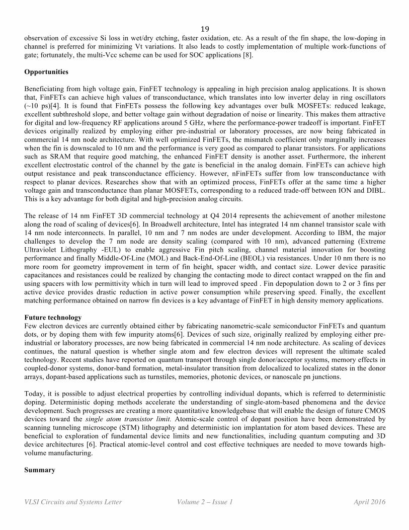
namely, gate length, fin width, and fin height. The device parasitic appear as most important performance limiter for FinFETs. Regular layout techniques allow a more accurate estimate of the circuit power and delay in early design steps. Under 10nm, following a top-down approach, we should find the design space that allows to meet speed and power targets, then explore the optimization of the geometry in combination with disruptive solutions such as air gap spacers and wrapped contacts, the benefits and drawbacks of increased fin height, and a design level solution consisting in fin depopulation[6]. The efficiency of each solution depends on the balance between interconnect and device parasitic. Another challenge of FinFET ICs are the ESD reliability. FinFET technologies were viewed as a potential roadblock for providing high ESD reliable ICs due to the 3D nature of the narrow Si fins which do not allow a large current conduction before thermal failure[7]. However, detailed assessment of common ESD structures such as diodes and grounded gate devices, has shown that ESD reliability is not a roadblock for FinFET-based products. Studying both SOI and bulk FinFETs, bulk FinFET was found to provide superior ESD performance due to the fin connection to the substrate. Focusing on sub-20-nm bulk FinFET technologies, emerging challenges are not limited to dealing with the smaller silicon volume of the fins and finer pitch, but also with the introduction of high mobility channels in the fins[7]. Providing a sufficient level of ESD protection to IC in FinFET technology is a challenging task, but far from a showstopper to introduce the FinFET technology for commercial products. The introduction of FinFET in the sub-20 nm CMOS technology nodes will face new ESD challenges due to limitations of the lithography and the introduction of novel material inside the FinFETs. Each of those challenges poses a threat to the intrinsic ESD robustness, and therefore need to be understood in order to provide adequate ESD solutions.
Fig. 2. Schematic cross section of SOI (left) and Bulk (right) FinFET devices.
In brief the challenges in manufacturing FinFET beyond those typical ones discussed is cost, lithography, MOL and self-aligned contacts, layout dependent effects, and DFM. The Si surface on fins appears different than in bulk as supported by
19
VLSI Circuits and Systems Letter Volume 2 – Issue 1 April 2016
observation of excessive Si loss in wet/dry etching, faster oxidation, etc. As a result of the fin shape, the low-doping in channel is preferred for minimizing Vt variations. It also leads to costly implementation of multiple work-functions of gate; fortunately, the multi-Vcc scheme can be used for SOC applications [8]. Opportunities Beneficiating from high voltage gain, FinFET technology is appealing in high precision analog applications. It is shown that, FinFETs can achieve high values of transconductance, which translates into low inverter delay in ring oscillators (~10 ps)[4]. It is found that FinFETs possess the following key advantages over bulk MOSFETs: reduced leakage, excellent subthreshold slope, and better voltage gain without degradation of noise or linearity. This makes them attractive for digital and low-frequency RF applications around 5 GHz, where the performance-power tradeoff is important. FinFET devices originally realized by employing either pre-industrial or laboratory processes, are now being fabricated in commercial 14 nm node architecture. With well optimized FinFETs, the mismatch coefficient only marginally increases when the fin is downscaled to 10 nm and the performance is very good as compared to planar transistors. For applications such as SRAM that require good matching, the enhanced FinFET density is another asset. Furthermore, the inherent excellent electrostatic control of the channel by the gate is beneficial in the analog domain. FinFETs can achieve high output resistance and peak transconductance efficiency. However, nFinFETs suffer from low transconductance with respect to planar devices. Researches show that with an optimized process, FinFETs offer at the same time a higher voltage gain and transconductance than planar MOSFETs, corresponding to a reduced trade-off between ION and DIBL. This is a key advantage for both digital and high-precision analog circuits. The release of 14 nm FinFET 3D commercial technology at Q4 2014 represents the achievement of another milestone along the road of scaling of devices[6]. In Broadwell architecture, Intel has integrated 14 nm channel transistor scale with 14 nm node interconnects. In parallel, 10 nm and 7 nm nodes are under development. According to IBM, the major challenges to develop the 7 nm node are density scaling (compared with 10 nm), advanced patterning (Extreme Ultraviolet Lithography -EUL) to enable aggressive Fin pitch scaling, channel material innovation for boosting performance and finally Middle-Of-Line (MOL) and Back-End-Of-Line (BEOL) via resistances. Under 10 nm there is no more room for geometry improvement in term of fin height, spacer width, and contact size. Lower device parasitic capacitances and resistances could be realized by changing the contacting mode to direct contact wrapped on the fin and using spacers with low permittivity which in turn will lead to improved speed . Fin depopulation down to 2 or 3 fins per active device provides drastic reduction in active power consumption while preserving speed. Finally, the excellent matching performance obtained on narrow fin devices is a key advantage of FinFET in high density memory applications. Future technology Few electron devices are currently obtained either by fabricating nanometric-scale semiconductor FinFETs and quantum dots, or by doping them with few impurity atoms[6]. Devices of such size, originally realized by employing either pre-industrial or laboratory processes, are now being fabricated in commercial 14 nm node architecture. As scaling of devices continues, the natural question is whether single atom and few electron devices will represent the ultimate scaled technology. Recent studies have reported on quantum transport through single donor/acceptor systems, memory effects in coupled-donor systems, donor-band formation, metal-insulator transition from delocalized to localized states in the donor arrays, dopant-based applications such as turnstiles, memories, photonic devices, or nanoscale pn junctions. Today, it is possible to adjust electrical properties by controlling individual dopants, which is referred to deterministic doping. Deterministic doping methods accelerate the understanding of single-atom-based phenomena and the device development. Such progresses are creating a more quantitative knowledgebase that will enable the design of future CMOS devices toward the single atom transistor limit. Atomic-scale control of dopant position have been demonstrated by scanning tunneling microscope (STM) lithography and deterministic ion implantation for atom based devices. These are beneficial to exploration of fundamental device limits and new functionalities, including quantum computing and 3D device architectures [6]. Practical atomic-level control and cost effective techniques are needed to move towards high-volume manufacturing. Summary
20
VLSI Circuits and Systems Letter Volume 2 – Issue 1 April 2016
The development of CMOS devices from planar MOSFET structure to double gate FinFETs are discussed. The performance of FinFET devices and their challenges in manufacturability are reviewed. The benefits of FinFET devices compared to planar devices are also discussed. Further developments on Nanometric scale devices i.e. from FinFETs to quantum dots - atom based device is introduced in this paper. References 1. Ieong, Meikei, HS Philip Wong, Edward Nowak, Jakub Kedzierski, and Erin C. Jones. "High performance double-
gate device technology challenges and opportunities." In Quality Electronic Design, 2002. Proceedings. International Symposium on, pp. 492-495. IEEE, 2002
2. Benjamin Colombeau , “Advanced CMOS devices:Challenges and implant solutions” Phys. Status Solidi A 211, No. 1, 101–108 (2014)
3. N. Collaert, S. Brus. Et al “ Integration challenges for multi-gate devices”, 2005 IEEE International Conference on
Integrated Circuit and Technology, pp 187-194 4. Vaidy Subramanian, et al, “Planar Bulk MOSFETS Versus FinFETs: An Analog/RF Perspective”, IEEE
TRANSACTIONS ON ELECTRON DEVICES, VOL. 53, NO. 12, DECEMBER 2006, pp. 3071-3079 5 Bardon, M. Garcia, P. Schuddinck, P. Raghavan, D. Jang, D. Yakimets, A. Mercha, D. Verkest, and A. Thean.
"Dimensioning for power and performance under 10nm: The limits of FinFETs scaling." In IC Design & Technology (ICICDT), 2015 International Conference on, pp. 1-4. IEEE, 2015.
6. Prati, Enrico, and Takahiro Shinada. "Atomic scale devices: Advancements and directions." Electron Devices Meeting
(IEDM), 2014 IEEE International. IEEE, 2014. 7. Linten, Dimitri, Geert Hellings, Shih-Hung Chen, and Guido Groeseneken. "ESD in FinFET technologies: Past
learning and emerging challenges." InReliability Physics Symposium (IRPS), 2013 IEEE International, pp. 2B-5. IEEE, 2013.
8. Chi, Min-hwa. "Challenges in Manufacturing FinFET at 20nm node and beyond." Technology Development, Global
foundries, Malta, NY, USA.[Online]. Available: http://www. rit. edu/kgcoe/eme/sites/default/files/Min-hwa% 20Chi (2012).
Updates
Upcoming Conferences/Workshops • iNIS: IEEE International Symposium on Nanoelectronic and Information Systems, Gwalior (India), Dec 19, 2016;
deadline: July 1, 2016; web: http://www.ieee-inis.org/ • PACT: International Conference on Parallel Architectures and Compilation Techniques, Israel, Sep 11-15, 2016;
deadline for workshops + tutorials: April 8, 2016; ACM Student Research Competition: June 17, 2016; web: http://pactconf.org/
• HPCS: International Conference on High Performance Computing & Simulation, Austria, July 18-22, 2016; deadline: March 22, 2016; web: http://hpcs2016.cisedu.info/
• APCCAS: Asia Pacific Conference on Circuits and Systems, Korea, Oct 25-28, 2016 ; deadline: April 29, 2016; web: http://apccas2014.org/
21
VLSI Circuits and Systems Letter Volume 2 – Issue 1 April 2016
• ISLPED: International Symposium on Low Power Electronics and Design, San Francisco, Aug 8-10/2016 ; deadline for Invited talk, panel, & embedded tutorial proposals: April 16, 2016; web: http://www.apccas2016.org/
• SBCCI: Symposium on Integrated Circuits and Systems Design, Brazil, Aug 29, 2016 – Sep 3, 2016; deadline: April 3, 2016; web: http://www.sbcci.org.br/
• SOCC : IEEE International System-on-Chip Conference, Washington, Sep 6-9, 2016; deadline: April 15, 2016; web: http://www.ieee-socc.org/
• VLSI-SoC: IFIP/IEEE International Conference on Very Large Scale Integration, Estonia, Sep 26-28, 2016; deadline: April 18, 2016; web: http://www.vlsi-soc.com/
• MWSCAS: IEEE International Midwest Symposium on Circuits and Systems, Abu Dhabi, Oct 16-19, 2016; deadline for special sessions and invited tutorials: May 2, 2016; web: http://events.kustar.ac.ae/mwscas2016/
• ICCAD: IEEE International Conference On Computer Aided Design, Texas, Nov 7 – 10, 2016; deadline: April 18, 2016; https://iccad.com/
• MICRO: IEEE/ACM International Symposium on Microarchitecture, Taiwan, Oct 15 – 19, 2016; deadline: April 3, 2016; web: http://www.microarch.org/micro49/
• ICM: IEEE International Conference on Microelectronics, Egypt, Dec 17 – 20, 2016; deadline: June 25, 2016; web: http://www.ieeeicm2016.org/
Award Information
iNIS 2015
• Student Travel Grants:
Name of the Student Title of Paper
Nalesh S.
Energy Aware Synthesis of Application Kernels expressed in Functional Languages on a Coarse Grained Composable Reconfigurable Array
Soumyajit Poddar Multicore ICs: Recent Trends in Developing Methodologies and Frameworks for Simulation
Wazir Singh Energy Efficient Analog-to-Information Converter For Biopotential Acquisition Systems
N Prasad ZMesh: An Energy-Efficient Network-onChip Topology for Constant-Geometry Algorithms
V Ramesh Kumar Accurate Numerical Model for Crosstalk Analysis of SWCNT Bundle Interconnects using FDTD Method
• Best Paper Awards
Author Names Title of Paper
Sauvagya Sahoo, Sudeendra Kumar, Kamala Kanta Mahapatra
Modified Configurable RO PUF with Improved Security Metrics
Sreeja Nair, Mary Regeena FinFETs and their application as load switches in micromechatronics
Kanchan Cecil, Jawar Singh Performance Enhancement of Dopingless Tunnel-FET based on Ge-source with High-k Dielectric
22
VLSI Circuits and Systems Letter Volume 2 – Issue 1 April 2016
ASYNC 2015 • Best paper award
Authors: E. Zianbetov, E. Beigné, and G. Di Pendina Title: Non-Volatility For Ultra-Low Power Asynchronous Circuits in Hybrid CMOS/Magnetic Technology
ASAP 2015 • Best paper award
Authors: Yongchao Liu and Bertil Schmidt Title: LightSpMV: Faster CSR-based Sparse Matrix-Vector Multiplication on CUDA-enabled GPUs • Best student paper award
Authors: Cecilia Gonzalez-Alvarez, Jennifer Sartor, Carlos Alvarez, Daniel Jimenez-Gonzalez and Lieven Eeckhout Title: Automatic Design of Domain-Specific Instructions for Low-Power Processors
ISVLSI 2015 • Amar Mukherjee best paper award:
Authors: Christian Brugger, Valentin Grigorovici, Matthias Jung, Christian Weis, Christian De Schryver, Katharina Anna Zweig, and Norbert When. Title: A Custom Computing System for Finding Similarities in Complex Networks,
• TCVLSI best paper award:
Authors: Ibtissem Seghaier, Mohamed H. Zaki, and Sofiene Tahar Title: A Statistical Approach to Probe Chaos from Noise in Analog and Mixed Signal Designs
• Honorable best paper award:
Authors: Fernando Cladera, Matthieu Gautier, and Olivier Sentieys Title: Energy-Aware Computing via Adaptive Precision under Performance Constraints in OFDM Wireless Receivers
• Best Poster award:
Authors: Matthias Hiller, Ludwig Kurzinger, Georg Sigl, Sven Muelich, Sven Puchinger and Martin Bossert Title: Low Area Reed Decoding in a Generalized Concatenated Code Construction for PUFs
• PhD Forum award:
1- Title: Translation Validation of Transformations of Embedded System Specifications using Equivalence Checking Authors: Kunal Banerjee, Chittaranjan Mandal, and Dipankar Sarkar
2- Title: Strategy on Removing Dark Silicon from VLSI Chip Authors: Zhou Zhao, Ashok Srivastava, Lu Peng, Shaoming Chen, Saraju P. Mohanty.
• Travel awards:
23
VLSI Circuits and Systems Letter Volume 2 – Issue 1 April 2016
1)Kaisheng Ma, Pennsylvania State University 2)Amr Sayed-Ahmed, University of Bremen 3)Anderson Sarto, Federal University of Rio Grande do Sul (UFRGS) 4)Mayukh Sarkar, Indian Institute of Engineering Science and Technology, Shibpur
ARITH 2015 • Best paper award
Authors: Nicolas Brunie, Florent de Dinechin, Olga Kupriianova, and Christoph Lauter Title: Code generators for mathematical functions
ECMS 2015 • Regular papers:
1st. FLEURMOND, R. (): A redundancy based control law for executing a coordinated vision-based task using a dual arm robotic systém 2nd. LANDKAMMER, S. (Regular paper): Static Modeling of an Antagonistic Pneumatic Actuator for Robotic Applications 3rd. GHENNA, S. (Regular paper): Modelling, identification and control of a Langevin transducer
• STUDENT PAPERS:
1st. KAHALERRAS, M.K. (): Analyses of temperature influence in piezoelectric transformers dedicated to plasma generation 2nd. NGUYEN, T.Ch. (S-18): Study on Incorporating Tone into Speech Recognition of Vietnamese
Call for Papers
Call for Participation: The 6th IEEE International Conference on Consumer Electronics – Berlin Wants You! Come and participate in the 6th IEEE International Conference on Consumer Electronics – Berlin, IEEE 2016 ICCE-Berlin, held 4 – 7 September 2016, once again in parallel with the IFA Consumer Electronics Exhibition, the leading trade show for Consumer Electronics and Home Appliances. An interesting program of oral and poster presentations is waiting for you, which also includes an industry track this year. We are again proud to present a number of interesting keynotes by well-known speakers in the field as well as tutorials and panel discussions. Moreover, a Doctoral Workshop is offered for PhD students, and a seminar and social event will be organized for Young Professionals. Tours of the IFA TecWatch and to the TiME Lab of the Fraunhofer Heinrich Hertz Institute will provide a glimpse into the future. Visit the web site www.icce-berlin.org to find the complete program and get more information about the conference.
24
VLSI Circuits and Systems Letter Volume 2 – Issue 1 April 2016
The ICCE-Berlin is the European sister conference of the IEEE Consumer Electronics Society’s flagship conference “ICCE” held annually in Las Vegas in conjunction with the Consumer Electronics Show (CES). Now in its 6th edition, ICCE-Berlin is well established and fully integrated in the IFA and continuously growing. This year again the IEEE CE Society is joining forces with other IEEE societies to broaden and strengthen the CE subjects and scope of the conference: the EMC Society, the Product Safety Engineering Society, the Reliability Society, the Life Sciences Technical Community, and the Society of Social Implications of Technology.
The conference will cover plenty of CE-relevant subjects such as audio and video technology, entertainment and games, car electronics, consumer networks, RF & wireless, human-device interaction, sports, wellness and home healthcare, smart energy, product safety engineering, and – new this time: sustainable electronics. It will again bring together researchers and engineers from industry, research centers, and academia to exchange information and results of recent work on systems, circuits, technologies, processes, and applications. It will provide an excellent forum for the researchers, system developers, and service providers to share their ideas, designs and experiences in such a proper environment as the IFA. Moreover, Berlin, a birthplace of consumer electronics, is one of Europe’s most exciting cultural centers and a vibrant city – and worth a visit on its own. • Visit us, discuss and network with colleagues from all over the world and with people from the largest
associations of consumer electronics. The Organizing Committee is looking forward to meeting you in Berlin for an exciting IEEE 2016 ICCE-Berlin!
25
VLSI Circuits and Systems Letter Volume 2 – Issue 1 April 2016
Outreach and Community
Are We Still Teaching VLSI the Same Way We Were in the Mid-90s? Mike Borowczak Erebus Labs and Consulting, Laramie, Wyoming USA Andrea Burrows Department of Secondary Education, University of Wyoming, Laramie, WY, USA
In this issue of the IEEE-CS TCVLSI newsletter the authors look at historical publication data for VLSI within education journals. The data suggests either a stagnation in VLSI educational approaches, or hopefully a simple lack of dissemination of our current best practices. Faculty and professionals are highly encouraged to send highlights of their outreach and unique educational activities for future issues! The Outreach and Community section ends with an encoding puzzle which you can share amongst your peers, colleagues and students. Correct entries, sent to the section editor, will be placed in a drawing for a prize and/or recognized on the TCLVSI website.
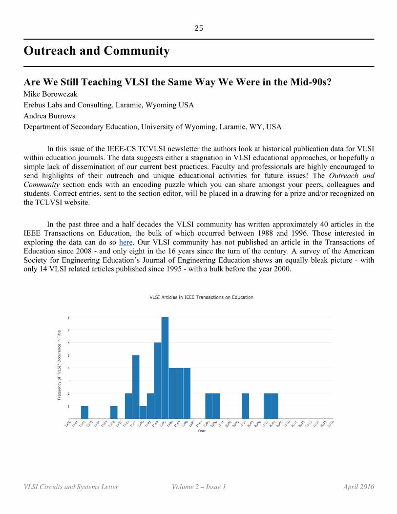
In the past three and a half decades the VLSI community has written approximately 40 articles in the IEEE Transactions on Education, the bulk of which occurred between 1988 and 1996. Those interested in exploring the data can do so here. Our VLSI community has not published an article in the Transactions of Education since 2008 - and only eight in the 16 years since the turn of the century. A survey of the American Society for Engineering Education’s Journal of Engineering Education shows an equally bleak picture - with only 14 VLSI related articles published since 1995 - with a bulk before the year 2000.
26
VLSI Circuits and Systems Letter Volume 2 – Issue 1 April 2016
With this empirical evidence we can only ask questions. Are our practices of educating our future VLSI experts keeping pace with the best known engineering education practices? If so, why have we not published results of our advances? Without a detailed survey of current practices, these questions will continue to remain a mystery. In this Outreach and Community section we depart from our typical format of highlighting a specific faculty member and instead present a short survey to our readership to assess the current state of educational practices in VLSI. TCVLSI members are encouraged to distribute this survey to their peers and students. Results will be shared in an upcoming issue of VCAL. The survey will be available April 2016 through June 2016 from the following site: http://bit.ly/tcvlsi-ed-survey.
Faculty Spotlight
Do you have outreach or educational experiences that you would like to share? If you would like to be featured in the next issue of TCVLSI’s newsletter, or if you would like to nominate someone to featured in the next issue send an email to [email protected] with details and contact information.
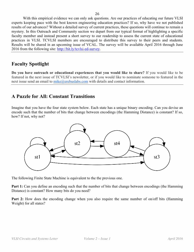
A Puzzle for All: Constant Transitions Imagine that you have the four state system below. Each state has a unique binary encoding. Can you devise an encode such that the number of bits that change between encodings (the Hamming Distance) is constant? If so, how? If not, why not?
The following Finite State Machine is equivalent to the the previous one.
Part 1: Can you define an encoding such that the number of bits that change between encodings (the Hamming Distance) is constant? How many bits do you need?
Part 2: How does the encoding change when you also require the same number of on/off bits (Hamming Weight) for all states?

27
VLSI Circuits and Systems Letter Volume 2 – Issue 1 April 2016
Use the google form located here bit.ly/pfa-ct to submit your answers to this puzzle. You’ll be added to a running scoreboard of correct submissions and be entered for a chance to win a prize.
Have a puzzle? Do you want to try to stump your colleagues? Send your puzzle ideas to [email protected] and you might see it featured here!

28
VLSI Circuits and Systems Letter Volume 2 – Issue 1 April 2016
Call for Contributions
The VLSI Circuits and Systems Letter aims to provide timely updates on technologies, educations and opportunities related to VLSI circuits and systems for TCVLSI members. The letter will be published twice a year and it contains the following sections: • Features: selective short papers within the technical scope of TCVLSI, “What is” section to introduce interesting
topics related to TCVLSI, and short review/survey papers on emerging topics in the areas of VLSI circuits and systems.
• Opinions: Discussions and book reviews on recent VLSI/nanoelectronic/emerging circuits and systems for nano computing, and “Expert Talks” to include the interviews of eminent experts for their concerns and predictions on cutting-edge technologies.
• Updates: Upcoming conferences/workshops of interest to TCVLSI members, call for papers of conferences and journals for TCVLSI members, funding opportunities and job openings in academia or industry relevant to TCVLSI members, and TCVLSI member news.
• Outreach and Community: The “Outreach K20” section highlights integrating VLSI computing concepts with activities for K-4, 4-8, 9-12 and/or undergraduate students. It also features student fellowship information as well a “Puzzle” section for our readership.
We are soliciting contributions to all these four sections. Please directly contact the editors and/or associate editors by email to submit your contributions.
Submission Deadline: All contributions must be submitted by September 1, 2016 in order to be included in the October issue of the letter.
Editors: • Saraju P. Mohanty, University of North Texas, USA, [email protected] • Xin Li, Carnegie Mellon University, USA, [email protected] Associate Editors: • Executive: Yiyu Shi, University of Notre Dame, USA, [email protected] • Features: Shiyan Hu, Michigan Technological University, USA, [email protected] • Features: Qi Zhu, University of California, Riverside, USA, [email protected] • Opinions: Prasun Ghosal, Indian Institute of Engineering Science and Technology, India, [email protected] • Opinions: Aida Todri-Sanial, CNRS-LIRMM, French, [email protected] • Updates: Helen Li, University of Pittsburg, USA, [email protected] • Updates: Anirban Sengupta, Indian Institute of Technology, Indore, India, [email protected] • Outreach and Community: Mike Borowczak, Erebus Labs & Consulting LLC, USA, [email protected]