D AMPS D-AMPS Pro/1 D-AMPS Pro ……... new the Professional Communication tool.

Michael David Bryant 1 11/1/07 ME 348C/392Q Mechatronics 1 University of Texas at Austin 1 Basic electronics Operational Amplifiers (Op-Amps) Op-Amp Features Other Op-Amp Specifications & Issues Amplifier Configurations Inverting amplifier Multiple Inputs: Sum Over Inverting Point Three Resistor Equivalent Feedback Network Non-inverting Amplifier Differential Amplifier Instrumentation Amplifier Design Guidelines Passive Element Filters Basic Op-Amp Active Filters Digital to Analog Converters (D/A) D/A: Weighted Current Sources D/A: R - 2R Ladder Network Sample and Hold Circuits Analog to Digital Converters (A/D) A/D Successive Approximation A/D Parallel (flash) converters Hybrid Digital/Analog Systems

Michael David Bryant 2 11/1/07 ME 348C/392Q Mechatronics 1 University of Texas at Austin 2
Purpose Amplify (boost) weak signal Remove noise or other unwanted signal components filtering common mode rejection Preprocess signal for later operations Attenuate high frequencies: anti-aliasing before A/D conversion

Michael David Bryant 3 11/1/07 ME 348C/392Q Mechatronics 1 University of Texas at Austin 3
Basic electronics Operational Amplifiers (Op-Amps)
| V+ | , | V- | usually between 0 and 25 volts

Michael David Bryant 4 11/1/07 ME 348C/392Q Mechatronics 1 University of Texas at Austin 4
Op-Amp Features 1. Very high gain | eo / ei | = A ≈ 106 to 108 2. Large bandwidth (MHz or more) 3. High input impedance Ri ≈ 100 kΩ to 100 MΩ (⇒ small input load currents) 4. Low output impedance Ro ≈ 101 to 102 Ω 5. Differential inputs ei = ea - eb 6. High Common Mode Rejection Ratio (CMRR) ≈ 50 to 100 dB. (dB = 20 log10 ) CMRR: same common mode signal eCM into ea & eb ⇒ tiny eo If channel a & b input impedances same, minimizes effect of signals induced on both channels (e.g. 60 Hz from building supply). Common Mode Gain: CMG = A/CMRR ( e.g., = 106 /105 ≈ 10). 7. Temperature dependent parameters: design to minimize effects. 8. Voltage Supply Rejection Ratio (VSRR) gauges effect of power supply drift & variations V+ and V- as equivalent input ei . 9. Input Offset voltage Voffset : Manufacturing imperfections & temperature variations ⇒ eo ≠ 0 when ei = 0 (violating desired eo = - A ei ). To correct, adjust Voffset :

Michael David Bryant 5 11/1/07 ME 348C/392Q Mechatronics 1 University of Texas at Austin 5
+
-
oe
V (or V )- +
+V
offsetV
Voffset allows low cost Op-Amp. Imperfections corrected (cheaply) at installation, not (expensively) during chip manufacture. 10. Op-Amp acts as controllable valve.
Output V- ≤ eo ≤ V+ ⇒ V-A ≤ - ei ≤
V+A .
11. Input bias currents I+ and I- (10 nA to µA) flow through + (b) and - (a) input terminals to bias input transistors (FET gate or BJT base). Voltage drop developed across input elements must be balanced (same at both terminals) so that eo = 0. ⇒ Balanced input resistances to + and - . 12. Input offset currents I+ and I- ⇒ residual eo ≠ 0 unless minimized with potentiometer on one input to fine tune. Can also adjust Voffset . Puts upper limit on values of input resistors (minimize voltage drops due to I+ and I- ).

Michael David Bryant 6 11/1/07 ME 348C/392Q Mechatronics 1 University of Texas at Austin 6 13. Class B operation often used in output stage: complementary npn & pnp in push/pull (Nearly identical amplifier circuits--stage 1 & stage 2-- arranged in parallel. Stage 1 amplifies only positive voltages, and switches off for negative. Stage 2 amplifies only negative, and switches off for positive.) Crossover distortions possible (small signals) in dead space as transistors in stages switch on/off.
oe
ie
dead space:
transistors on/off
stage 1:
positive
response
stage 2:
negative
response

Michael David Bryant 7 11/1/07 ME 348C/392Q Mechatronics 1 University of Texas at Austin 7
Other Op-Amp Specifications & Issues
A. Slew rate SR ≡ deodt max important to avoid large signal
distortions. ei = E sin ωt ; SR = E ω cos ωtmax = E ω Require SR ≥ 2π f E for amp to follow largest voltage swing. B. Compensation: Lead/lag network to control phase margin when negative feedback. For stable amplifier design gain ( -R2R1 for inverting amplifier, 1 + -
R2R1 for noninverting
amplifier), require closed loop response curve to meet open loop curve where slope of closed loop curve is -20 dB/dec. - 20dB/dec ⇒ 1st order term ⇒ - 90° phase ⇒ limited signal growth (phase margin = 180° - 90° = 90°⇒ stable closed loop system) Internally compensated: manufacturer provides network for -20 dB/decade; limits bandwidth but unconditionally stable. Externally compensated: Install capacitance (≈ pF) across indicated frequency compensation terminals to control bandwidth and closed loop gain (-40 dB ⇒ -20dB). Manufacturer specifies needed capacitance. Conditionally stable (for given closed loop gain).
f (Hz)
MdB
1 M1k
open loop: gain A
uncompensated: unstable design(closed loop design crosses -60 dB/dec)
internally compensated:
unconditionally stable(-20 dB/dec up to 100kHz)
externally compensated:
stable design (crosses -20 dB/dec)
40
0
120 -20 dB/dec-20 dB/dec
-40 dB/dec
-60 dB/dec
design gain:
closed loop-20 dB/dec
80
open loop at -20 dB/dec
meets closed loop gain

Michael David Bryant 8 11/1/07 ME 348C/392Q Mechatronics 1 University of Texas at Austin 8
Unstable Feedback Oscillation: Sinusoid grows
+
-G
Hinput sine
output sine: Gcauses phase lag
additional phase lagof H inverts sine
First cycle: No feedback, but GH inverts. First cycle: Negative feedback & GH inversion (- 360° phase) add constructively with input.
+
-G
H
After second pass, feedback promotes signal growth. Further passes ⇒ unstable!

Michael David Bryant 9 11/1/07 ME 348C/392Q Mechatronics 1 University of Texas at Austin 9
C. Power Supply Filter Capacitors (10-1 to 1 µF) to minimize power supply fluctuations
V-
+V
0.1 µF
0.1 µF

Michael David Bryant 10 11/1/07 ME 348C/392Q Mechatronics 1 University of Texas at Austin 10
Amplifier Configurations Inverting amplifier
+
-1
R
2
R
oes
e
3
R
be
aei
1
i2
i3
a. DC analysis DC biases: Very large Ri ⇒ e
DCab ≈ 0 ⇒ e
DCa ≈ e
DCb
Small bias current iDC3 ≈ 0 ⇒ e
DCb = - i
DC3 R3 ≈ 0
⇒ eDCa ≈ 0 : node a at virtual ground!
Negative feedback (via R2 ) enhances.

Michael David Bryant 11 11/1/07 ME 348C/392Q Mechatronics 1 University of Texas at Austin 11
b. R3 = R1 R2 = R1 R2
R1 + R2 to balance input bias
current voltage drop:
If R3 = 0, eDCa ≈ e
DCb = 0 ⇒ i
DC1 = 0 & i
DC2 =
eDCo - e
DCa
R2
⇒ eDCo = i
DC2 R2 ≠ 0
Required: zero input es = 0 ⇒ eo = eDCo + e
ACo = 0.
Achieved via R3 = R1 R2 (balanced bias currents i3
DC = i1DC + i2
DC ) . c. AC signal analysis Currents into – inverting terminal negligible (very large Ri ) ⇒ i1 ≈ - i2
⇒ es - ea
R1 = - eo - ea
R2 ,
with eo = - A ei = - A ( ea - eb )= - A ea
eoes = - A
1 + R1/R2 (1 + A) ≈ -R2 /R1 at low freq, A >> 1
breaks down at high freq, A = A(f) & Ri = Ri(f)
d. Input resistance Rin = esi1 =
es R1es - ea ≈ R1 at low
frequency
e. Output resistance Rout ≈ - Ro ( 1 + R1/R2 )
A small
(10-1 to 100 )

Michael David Bryant 12 11/1/07 ME 348C/392Q Mechatronics 1 University of Texas at Austin 12
Multiple Inputs: Sum Over Inverting Point
+
-12
R
2
R
oe
1e
3
R
2e
3e
13
R
11
R i1
be
aei
2
i3
eo ≈ -R2 e1
R11 + e2
R12 +e3
R13
R3 =(R11 R12 R13 ) R2

Michael David Bryant 13 11/1/07 ME 348C/392Q Mechatronics 1 University of Texas at Austin 13
Three Resistor Equivalent Feedback Network
+
-1
R
2b
R
oe
se
3
R
be
aei
2c
R
2a
R
Equivalent feedback resistor R2 = R2a + R2b + R2a R2b /R2c Small R2c ⇒ large equivalent R2 without big (noisy) resistors For higher gain Op-amp designs

Michael David Bryant 14 11/1/07 ME 348C/392Q Mechatronics 1 University of Texas at Austin 14
Non-inverting Amplifier
+
-1
R
2
R
oe
se
3
R
R3 = R1 R2 a. Input on non-inverting + terminal, feedback to inverting - terminal for stability
b. eoes = A
1 + A R1/(R1 + R2 )
≈1 + R2 /R1 @ low freq, A >> 1
c. Input resistance Rin ≈ Ri A
1 + R2/R1 >> Ri
extremely large d. Output resistance Rout same as inverting amp.

Michael David Bryant 15 11/1/07 ME 348C/392Q Mechatronics 1 University of Texas at Austin 15
Differential Amplifier
4Rs2
e
+
-1R
2R
oe
s1e
3R
a. Common mode rejected (e.g., drift) via high CMRR R3 = R1
b. eo ≈ R4
R3 + R4 ( 1 + R2R1 ) es2 -
R2R1 es1 =
R2R1 ( es2 - es1 )
R4 = R2
c. R-in = R1 (small) R+
in ≈ R3 + R4 (small)

Michael David Bryant 16 11/1/07 ME 348C/392Q Mechatronics 1 University of Texas at Austin 16
Instrumentation Amplifier
+
-
4R
s2e
+
-
1R
2R
oe
s1e
3R
2R
3R
+
-
4R
Combine advantages: High input impedance / non-inverting terminals Differential stage (CMRR)

Michael David Bryant 17 11/1/07 ME 348C/392Q Mechatronics 1 University of Texas at Austin 17
Design Guidelines A. Op-Amp selection Gain & bandwidth within scope of amp design Peak to Peak output voltage swing within range of supply rails (V+ , V- )
Slew rate SR ≥ dvdt max
Acceptable noise figure (NF) over operating range B. Stability frequency compensation (internal or external) for - 20 dB/dec external: resisitors and capacitors specified by manufacturer - 20 dB/dec. at desired gain ⇒ stable amplifier C. Power supply Supply rails V+ , V- sufficient for swings minimize power supply fluctuations with filter capacitors avoid draining: power peaks sufficient V+ , V- not too high: excessive shot noise

Michael David Bryant 18 11/1/07 ME 348C/392Q Mechatronics 1 University of Texas at Austin 18 D. Resistor selection Rin = R1 Rmin < R1 < Rmax Rmin lower bound from signal source (i, v) impedance: want high Rmax limited by offset current (⇒ DC drop at output) & thermal noise
Voca = [R1 ||R2 ioc ]max < 10% max allowed
distort; oc: offset current R2 /R1 gain for inverting amp, 1 + R2 /R1 for non-inverting amp R3 = R1 || R2 Networks (manufacturer) voltage offset compensation E. Offset ( defined by ei = 0 ⇒ eo ≠ 0 )
Voca << Voffset
Voffset reduced via voltage offset temperature dependence within operating range zero at Toperating δVout for δT < allowable distortion F. Distortion components (total < allowable) common mode / bias current (CMRR) Voc δVout power supply fluctuations (VSRR) insufficient bandwidth, slew rate, supply rails

Michael David Bryant 19 11/1/07 ME 348C/392Q Mechatronics 1 University of Texas at Austin 19
Passive Element Filters T network π network
Z1/2 Z1/2
Z2 Zload
.
2 Z2
Z1
Zload
.
2 Z2
Goal: overall impedance = Zload Capacitor: C , Inductor: L , low cutoff frequency: fl , high cutoff frequency: fh Designs: Low pass: Z1 = L, Z2 = C, fl = 0, fh =
1
! LC
High pass: Z1 = C, Z2 = L, fl =
1
4! LC, fh = ∞
Bandpass: Z1 = L1 series C1 , Z2 = L2 || C2 , fl , fh depend on Zload Bandreject: Z1 = L1 || C1 , Z2 = L2 series C2 , fl , fh depend on Zload

Michael David Bryant 20 11/1/07 ME 348C/392Q Mechatronics 1 University of Texas at Austin 20
Basic Op-Amp Active Filters 1st order active filter
+
-1
R
2
R
oe
se
3
R
C
Inverting amp with feedback C & R2 :
H(s) = eo(s)es(s) ≈ -
R2 || 1/sCR1 = -
R2/R1R2 C s + 1
low frequency gain: R2R1
3 dB cutoff frequency: fc = 12π R2 C

Michael David Bryant 21 11/1/07 ME 348C/392Q Mechatronics 1 University of Texas at Austin 21 2nd order active filter, Low gain type
+
-
1
R
oes
e
a
R
2
R
2
C
1
C
b
R
Non-inverting amp with coupling capacitors. Low
frequency gain: K = 1 + RbRa
H(s)=eo(s)es(s) = K
s2 R1R2C1C2 + s [R2 C1 + R1C1 + (1 - K) R1C2] + 1
cutoff (natural) frequency: fc = 12π R1R2 C1 C2

Michael David Bryant 22 11/1/07 ME 348C/392Q Mechatronics 1 University of Texas at Austin 22 2nd order active filter, High gain type
+
-1
R
oes
e
3
R
2
R
2
C
1
C
4
R
Inverting amp with feedback C2 ||(R4 + R2 ), input R1 + R2 , coupling capacitor C1
H(s) = eo(s)es(s)
= - 1/R1R2C1C2
s2+ s [1/R1 + 1/R4+ 1/R2](1/C1) + 1/R4R2C1C2
cutoff (natural) frequency: fc = 12π R4R2 C1 C2
Higher order filters usually cascade 1st & 2nd order filters

Michael David Bryant 23 11/1/07 ME 348C/392Q Mechatronics 1 University of Texas at Austin 23
Analog Integrator Inverting amp with feedback C & input R Replace feedback R with impedance 1/sC:
!
H(s) =eo(s)
eI(s)
= "1/sC
R= "
1
sRC
Integrator:
!
eo(t) = "
1
RCeo(t)dt#

Michael David Bryant 24 11/1/07 ME 348C/392Q Mechatronics 1 University of Texas at Austin 24
R2R Resistance Ladder Enables digital (software) control of resistance Input resistance can be changed in-situ Vi
2R
R R
2R 2R 2R
Vo
Z
operation switches control currents to terminals: non-inverting (ground) inverting terminals (virtual ground) total ladder current constant currents half (left to right), each ladder step resistance into op-amp looking into any node: R 2R || 2R currents split in half

Michael David Bryant 25 11/1/07 ME 348C/392Q Mechatronics 1 University of Texas at Austin 25
Digital to Analog Converters (D/A or DAC) Converts digital (binary number) to analog voltage
Settling time ts : time required for analog input (voltage or current) to settle within ± LSB/2 following input code change typical: nsec to 100 µsec circuits downstream add dynamics ⇒ increases ts

Michael David Bryant 26 11/1/07 ME 348C/392Q Mechatronics 1 University of Texas at Austin 26
D/A: Weighted Current Sources
1, Sk closed
Switch function ak = controlled by bit settings
0, Sk open "Bit" currents ik sum, give output:
Vo = - Vs R2 ∑k=0
3 ak/R1k
Problems: Many bits ⇒ many resistors Usually R1k = 2k R for binary powers requires accurate resistors: each resistor must be precisely 1/2 its neighbor

Michael David Bryant 27 11/1/07 ME 348C/392Q Mechatronics 1 University of Texas at Austin 27
DAC: R2R Ladder Network
R2R Ladder Network DACs in 8, 10, 12, 14, 16, or 18 bits Output Vo more accurate: only 2 resistor values needed similar to weighted current source: currents in powers of 2 noninverting terminal at ground, inverting terminal at virtual ground ⇒ ladder currents constant, independent of switches Example: 4 bit D/A (Bits 3 ,2, 1, 0) 2 R i0 =V0 =2 R it ⇒ i0 = it 2 R i1 =V1 =R( i0 + it )+V0 ⇒ i1 = 2 i0 2 R i2 =V2 =R( i1 + i0 + it )+V1 ⇒ i2 = 2 i1
i = ∑k=0
3ak ik ; Vo = - ∑
k=0
3 ak
R22 R Vk = -R2 ∑
k=0
3ak ik = -R2 i
Michael David Bryant 28 11/1/07 ME 348C/392Q Mechatronics 1 University of Texas at Austin 28
Sample and Hold Circuits
+
-
oViD
MOSenhancement
FET
G
DS
C
+
-
+ 5 V
-V
+V
Analoginputvoltage
control
signal comparator high: sample
low: hold
from CPU via
control register
voltage follower (R = 0)2
buffered output
(same V but
larger i)
In higher performance A/D converters Operation (Sample & Hold Input during A/D conversion) switch (FET) closes & analog voltage charges capacitor capacitor voltage to Op-Amp constant (held) after switch opens
MOSFET: Positive gate voltage attracts electrons (charge carriers) into channel, increasing conductance FET "switch" characteristics VGS low ⇒ 10 MΩ (open switch) VGS high ⇒ 200 Ω (closed switch)
10
20
i (mA)D 7V
5V
V = 4VGS
V = 0VGS
V (V)DS5 10
200 ! = 2V/10 mA
10 M!

Michael David Bryant 29 11/1/07 ME 348C/392Q Mechatronics 1 University of Texas at Austin 29 Comparator: Special Op-Amp circuit prone to saturation, but optimized for fast recovery from saturation V+ (high), V1 > V2
Vout =
V- (low), V1 < V2
.
+
-
outputvoltage
comparator
V1
V2
Michael David Bryant 30 11/1/07 ME 348C/392Q Mechatronics 1 University of Texas at Austin 30
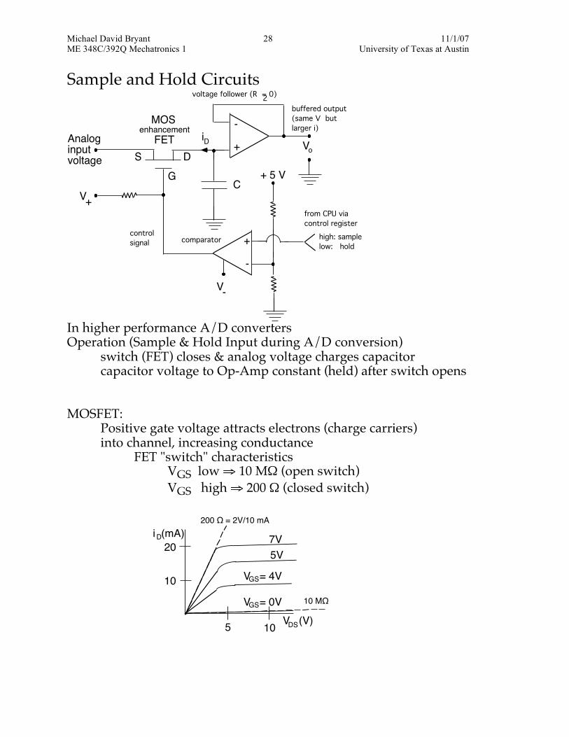
Analog to Digital Converters (A/D or ADC) Convert analog voltage to digital (binary) 1) A/D Successive Approximation
.
+
-
comparator
B1B2B3 B0
4 bit D/A
clock
startD
control logic
voltage limitingdiode pair
V /Rin
R
Vin
analog inputfrom sample& hold
a b
MSB
LSB
Itest
I
Input frozen by sample & hold
Diodes limit Vd swing due to I = VinR - I test
series of n (# bits) bit tests places input in bin (voltage range) D/A converter generates test currents I test (or voltages) , to be compared to input final D/A number = A/D result I test reflects current D/A setting
I = VinR - I test ⇒ Vd ⇒ high or low logic
I
Vd
a
a b
b

Michael David Bryant 31 11/1/07 ME 348C/392Q Mechatronics 1 University of Texas at Austin 31 Test sequence, 4 bit A/D ⇒ 4 tests test bit tested D/A test setting bit test result 1 3 (MSB) 0111 a3 2 2 a3 011 a2 3 1 a3 a2 01 a1 4 0 (LSB) a3 a2 a1 0 a0 1, Vd > 0 ⇒ I test < Vin /R
ak = 0, Vd < 0 ⇒ I test > Vin /R Bit test result ak causes D/A to output current I test that CANCELS a component of input current Vin /R, thereby fine tuning D/A register. Final result a3 a2 a1 a0 . Problem: accurate but moderate speed. Conversion times 1 µs to 100 µs.

Michael David Bryant 32 11/1/07 ME 348C/392Q Mechatronics 1 University of Texas at Austin 32
Capacitor Based Successive Approximation
• Charge all capacitors to Vin o lower plate = input voltage Vin o upper plate = ground
• For ADC, Switch o leftmost C (MSB) to +Vref o other C’s to -Vref o ground switch open
• Comparator determines if

Michael David Bryant 33 11/1/07 ME 348C/392Q Mechatronics 1 University of Texas at Austin 33
A/D Parallel Flash ADC converters
.
+
-
+
-
+
-
decoding logic( 1 level)
Vin
MSB
LSB
latch (switches on)
R
R
R
Vref
2/3 Vref
1/3 Vref
Speeds exceed 500 MHz: up to 4 GHz for 4 bit converter Voltage dividing resistors R create 2n voltage levels or “bins” Comparators ⇒ which "bin" contains input Big Problem: need (2n -1) resistors & comparators for 2n bins ⇒ requires large silicon area on chip ⇒ usually limited to 3 to 6 bits Other problems: parasitic capacitance at each resistor limits bandwidth many resistors increase power consumption
Michael David Bryant 34 11/1/07 ME 348C/392Q Mechatronics 1 University of Texas at Austin 34
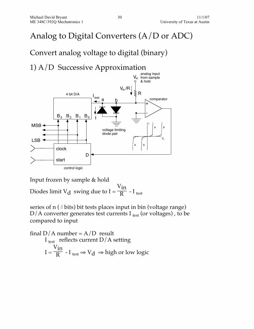
Pipelining
• Sample & Hold (S/H) • Multiple conversion stages • 1 or 2 bit conversions @ each stage
o Flash converters do ADC o DAC converts bits to voltage o Subtract bit voltage from input, create residue o Amplify residue o Next stage does next bits o Order: MSB to LSB
• Pipeline: Samples flow through, 1 stage at a time Advantages N to 2N COMPARATORS High sampling frequency, with > 8 bits Drawbacks Complexity Power consumption

Michael David Bryant 35 11/1/07 ME 348C/392Q Mechatronics 1 University of Texas at Austin 35
Sigma Delta ΣΔ (Delta Sigma ΔΣ) Converters For low frequency signals Output: pulses of constant
amplitude & duration Interval between pulses
proportional to input voltage. Higher input voltage @ 1 ⇒ Greater slope of integrator
output (~ramp) voltage @4 ⇒ More frequent comparator
triggers & spikes @5 ⇒ Shorter intervals between
pulses @2 & @3
Count pulses: count ~ input voltage

Michael David Bryant 36 11/1/07 ME 348C/392Q Mechatronics 1 University of Texas at Austin 36
Hybrid Digital/Analog Systems Noise perspective: analog & digital systems incompatible analog contaminated by digital pulses ⇒ AC noise via power supply feedback stray C 's ground loops digital contamination analog ⇒ lower frequency filtering reduced digital pulses Prescription: Isolate systems 1. Separate analog & digital grounds 2. Connect digital & analog at ONE point ONLY (avoid ground loops) 3. Provide separate analog & digital supply voltages 4. Electrostatic shielding (Faraday cage) around analog circuit. Connect one end only to analog ground 5. At especially sensitive interconnections, consider electro-optic coupling 6. Consider using emitter coupled logic (ECL) in digital section for less spurious signal generation 7. If analog & digital on same IC, separate with wells (pn junctions)