1 Ballisticity of the Linear response Transport in Nanometric Silicon Devices C. Jungemann Institute...
16
1 Ballisticity of the Linear response Transport in Nanometric Silicon Devices C. Jungemann Institute for Electronics Bundeswehr University Neubiberg, Germany EIT4
-
date post
21-Dec-2015 -
Category
Documents
-
view
217 -
download
2
Transcript of 1 Ballisticity of the Linear response Transport in Nanometric Silicon Devices C. Jungemann Institute...

1
Ballisticity of the Linear response Transport in Nanometric Silicon Devices
C. Jungemann
Institute for Electronics
Bundeswehr UniversityNeubiberg, Germany
EIT4

2
Outline
• Introduction
• Theory
• Results for 40nm N+NN+ structure– High bias– Zero bias
• Conclusions

3
Introduction

4
Introduction
1D 40nm N+NN+ structure
5 1019cm-3 2 1017cm-3 5 1019cm-3
0 10 50 60[nm]
• Macroscopic models (DD, HD) fail for strong nonequilibrium due to
Ballistic transport!
• Macroscopic models also fail near equilibrium in nanometric devices!
Why?

5
Theory
6
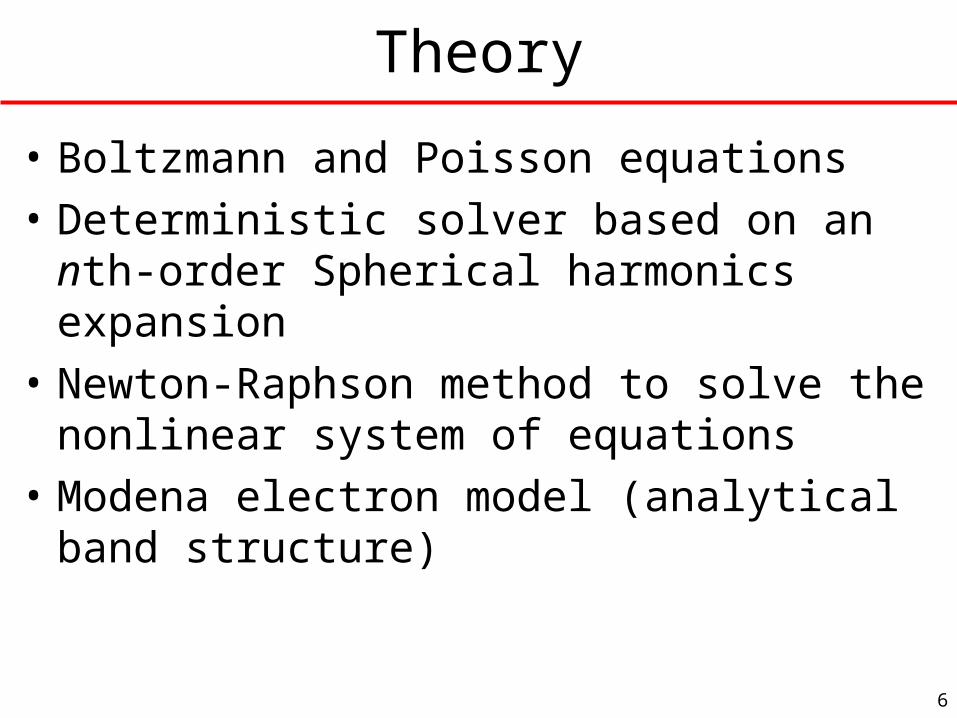
Theory
• Boltzmann and Poisson equations
• Deterministic solver based on an nth-order Spherical harmonics expansion
• Newton-Raphson method to solve the nonlinear system of equations
• Modena electron model (analytical band structure)

7
Theory
3s
r 3k
Boltzmann equation (steady state, neglecting the valley index, spherical bands):
eE(r) f (r, k) v(k) f (r, k) W(r,k | k ')f (r, k ') W(r, k ' | k)f (r, k)d k '
2
Projection of the distributio
3l,m l,m3
l
l,
0,0
m l,ml 0 m l
0
1,1
n function onto spherical harmonics:
2g (r, ) (k) Y (k), (k) f (r, k)d k
2
g (r, )Y ,
Electron density:
n(r) 4 g (r, )d
Current density
g
:
g4
j(r) v( )3
(r, , , )
1
0
, 1
1,0
(r, )
g (r, ) d
g (r, )

8
Results
1D 40nm silicon N+NN+ structure
Transport is in x-direction
9
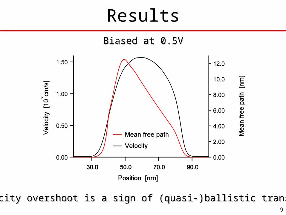
ResultsBiased at 0.5VBiased at 0.5V
Velocity overshoot is a sign of (quasi-)ballistic transportVelocity overshoot is a sign of (quasi-)ballistic transport

10
ResultsBiased at 0.5VBiased at 0.5V Quasi-ballisticQuasi-ballisticScattering dominatedScattering dominated

11
Results
Distribution function at 0.5VDistribution function at 0.5V
2
l 0
1 l
l,m l,mm l
g(r, , , ) g (r, )Y ,

12
Results
Distribution function at 0.5VDistribution function at 0.5V
2
l 1
1 l
l,m l,mm l
g(r, , , ) g (r, )Y ,

13
Results
Quasi-ballisticQuasi-ballisticScattering dominatedScattering dominated Linear responseLinear responsewithout zero orderwithout zero order

14
Results
21 l
l,ml,m
m ll 1
g (r, )g(r, , , )Y ,
V V
Differential distribution function at equilibriumDifferential distribution function at equilibrium

15
Conclusions
16
Conclusions
• Ballistic transport occurs in nanometric devices at high bias
• The linear response of the distribution function shows ballistic peaks at zero bias in regions with large built-in fields
• The ballistic peaks of the linear response can be negative
• Linear response in nanometric devices with large built-in fields is fundamentally different from the bulk case