An Energy-Efficient Architecture for Nanometric ...
14
HAL Id: hal-00675609 https://hal.archives-ouvertes.fr/hal-00675609 Submitted on 1 Jun 2013 HAL is a multi-disciplinary open access archive for the deposit and dissemination of sci- entific research documents, whether they are pub- lished or not. The documents may come from teaching and research institutions in France or abroad, or from public or private research centers. L’archive ouverte pluridisciplinaire HAL, est destinée au dépôt et à la diffusion de documents scientifiques de niveau recherche, publiés ou non, émanant des établissements d’enseignement et de recherche français ou étrangers, des laboratoires publics ou privés. An Energy-Effcient Architecture for Nanometric Technologies with Strong Robustness to Process Variability: Design of a GALS node based on a MIPS R2000 processor Sylvain Durand, H. Zakaria, Laurent Fesquet, Nicolas Marchand To cite this version: Sylvain Durand, H. Zakaria, Laurent Fesquet, Nicolas Marchand. An Energy-Effcient Architecture for Nanometric Technologies with Strong Robustness to Process Variability: Design of a GALS node based on a MIPS R2000 processor. [Research Report] GIPSA-lab. 2013. hal-00675609
Transcript of An Energy-Efficient Architecture for Nanometric ...

HAL Id: hal-00675609https://hal.archives-ouvertes.fr/hal-00675609
Submitted on 1 Jun 2013
HAL is a multi-disciplinary open accessarchive for the deposit and dissemination of sci-entific research documents, whether they are pub-lished or not. The documents may come fromteaching and research institutions in France orabroad, or from public or private research centers.
L’archive ouverte pluridisciplinaire HAL, estdestinée au dépôt et à la diffusion de documentsscientifiques de niveau recherche, publiés ou non,émanant des établissements d’enseignement et derecherche français ou étrangers, des laboratoirespublics ou privés.
An Energy-Efficient Architecture for NanometricTechnologies with Strong Robustness to Process
Variability : Design of a GALS node based on a MIPSR2000 processor
Sylvain Durand, H. Zakaria, Laurent Fesquet, Nicolas Marchand
To cite this version:Sylvain Durand, H. Zakaria, Laurent Fesquet, Nicolas Marchand. An Energy-Efficient Architecturefor Nanometric Technologies with Strong Robustness to Process Variability : Design of a GALS nodebased on a MIPS R2000 processor. [Research Report] GIPSA-lab. 2013. hal-00675609

MANUSCRIPT SUBMITTED TO CIRCUITS AND SYSTEMS I: REGULAR PAPER, ON DECEMBER 1, 2011 1
An Energy-Efficient Architecture for Nanometric Technologieswith Strong Robustness to Process Variability:Design of a GALS node based on a MIPS R2000 processor
Sylvain Durand, Hatem Zakaria, Laurent Fesquet and Nicolas Marchand
Abstract—In this paper we present an energy-efficient solu-tion for nanometric systems, where some variability problemswhich did not influence the circuit at a higher scale introducesome uncertainties at a sub-micrometric size. Therefore, someadvanced control strategies are required to manage the energy-performance tradeoff in such an environment. The setup is basedon some Dynamic Voltage and Frequency Scaling (DVFS) tech-niques applied to a Globally Asynchronous Locally Synchronous(GALS) architecture. Whereas a Vdd-hopping converter is able toprovide discrete voltage levels, a Programmable Self-Timed Ring(PSTR) oscillator allows a variability robust source for generatingadjustable clock frequencies. A fast predictive control law is alsodeveloped in this paper to calculate the frequency and voltagelevels to apply to these actuators, minimizing the high voltagerunning time while ensuring good computational performance.Finally, the proposal is dedicated to a GALS node based on aMIPS processor over STMicroelectronics 45 nm technology andsome fine-grained simulation results are performed. Besides anoticeable reduction of the energy consumption, the performanceof the closed-loop system is ensured and a strong robustness totechnological variability is also demonstrated.
Index Terms—Energy-performance tradeoff, nanometricGALS architecture, process variability robustness, fastpredictive control, programmable self-timed ring oscillator.
EDICS Category—CTRL100A5, POW170B0, DCS160-210.
INTRODUCTION
The upcoming generations of embedded integrated systemsin multimedia and telecommunication applications require sev-eral drastic technological evolutions since they have reachedlimits in terms of power consumption, computational effi-ciency and fabrication yield. As a result, the main problemsthat we are facing nowadays with the nanometric technologiescan be categorized in three main points:
a) Variability refers to the unpredictability, inconsistency,unevenness, and changeability associated with a given featureor specification. At a sub-micrometric scale, variability hasbecome one of the leading causes for chip failures and delayedschedules. Indeed, in nanometric design flows, variability isassociated with design modes, power states, environmentalconditions, manufacturing steps, and the behavior of devicesand interconnects. Variability affects the entire physical de-sign environment, from power management, through timingand signal integrity closure to manufacturability. A major
S. Durand is with the NeCS project-team, an INRIA Rhone-Alpes andGIPSA-lab joined team, Grenoble, France ([email protected])
H. Zakaria is with the Electrical Engineering Department, Benha Faculty ofEngineering, Benha University, Benha, Egypt ([email protected])
L. Fesquest is with the CIS Group, TIMA Laboratory, Grenoble University,Grenoble, France ([email protected])
N. Marchand is with the SysCO team, Control Department of GIPSA-lab,Grenoble University, Grenoble, France ([email protected])
problem facing the computer and semiconductor industries isthe increasing CMOS process variability. In low-level circuitparameters, such as transistor gate length and gate oxide thick-ness, variability complicates system design by introducinguncertainty about how a fabricated system will perform [1].Although a circuit or chip is designed to run at a nominalclock frequency, the fabricated implementation may vary farfrom this expected performance (see Fig. 1).
b) Leakage power is a growing concern in the overalldesign process. As voltages scale downward with geometries,threshold voltages must also decrease to gain performanceadvantages of the new technology. This reduction in thresholdvoltages has led to an exponential increase in leakage currentin transistors. Thinner gate oxides have led to an increase ingate leakage current as well. At 65nm and below, leakagepower accounts for a significant portion of the total powerin high-performance designs [2], therefore its management isessential in the ASIC design process. Unlike dynamic power,which can be managed by reducing switching activity, leakagepower effect exists as long as the power is on. That is whycurrent process technologies are pushing designers to considernew design methods to reduce leakage power.
c) Yield success is much harder to achieve because ofthe increasing number and complexity of variables affectingmanufacturability. Early on, the path to yield on integratedcircuit design was fairly simple: comply with all the designrules and yield would more or less follow. Designers did notneed to worry too much about what happened in the fabricationafter tape-out [3]. Nevertheless, the game has changed in thenanometric era. The designer’s strategy must now shift fromsimple design rule compliance to the definition and design ofthe optimal layout for the highest yield.
Manager
speed
Fig. 1. Representation of the technological variability’s phenomenon whichappears in sub-micrometric integrated circuits: whereas a part of the chipcould run with the expected computational speed, another part may run moreslowly and another might not run at all. A controller has hence to managethese different domains to yield the best performance.

MANUSCRIPT SUBMITTED TO CIRCUITS AND SYSTEMS I: REGULAR PAPER, ON DECEMBER 1, 2011 2
Regarding the previously mentioned motivations, one canconclude the suggested solutions in two main points. First,the chips in advanced technologies require a dynamic powermanagement in order to highly reduce the energy consumption.Also, some architectural issues are needed for helping theyield enhancement of such circuits with strong technologicaluncertainties.
A. Power management technique
In today’s technology nodes, leakage power is a significantcontributor to the total power, as the gate length and thresholdvoltage are scaled down. Several techniques can be appliedat the circuit level to reduce leakage power, including multi-threshold libraries, power gating and variable body biasing [4],[5]. However, in current CMOS integrated circuits, the averagepower consumption and the energy dissipation are dominatedby the dynamic power, that arises from the charging anddischarging of the load capacitance:
Pavg(t) ∝ Cfclk(t)Vdd(t)2
E(t) ∝ CVdd(t)2 (1)
where C is the load capacitance, Vdd is the supply voltageand fclk is the clock frequency. These equations suggest thatminimizing the load capacitance, reducing the supply voltageor slowing the clock can reduce power and energy. Whilethe load capacitance can only be reduced during chip design(for example by minimizing on chip routing capacitancesand reducing external component access), voltage scalableprocessor and power controllable peripheral devices makepossible to manage power by a dedicated digital hardwareor by an Operating System (OS). For instance, the OS cancontrol the processor frequency and its voltage and/or putthe devices in low-power sleep states using a dynamic powermanagement [6]. The power minimization can be achievedby resolving an off-line stochastic optimization problem butthis is not always possible. Therefore the optimization hasto be performed on-line by the control system dedicatedto the power management. These techniques run slower theprocessors at a reduced voltage according to the instantaneouscomputational demand.
As previously shown in (1), reducing the frequency fclk andthe supply voltage Vdd decreases the energy and the power.The energy reduction is a quadratic function of the voltage anda linear function of the clock frequency. As a result, DynamicVoltage Scaling (DVS) can be used to efficiently manage theenergy consumption of a device [7]. Supply voltage can bereduced whenever slack is available in the critical path, but onehas to take care that scaling the voltage of a microprocessorchanges its speed as well. Therefore, adapting the supplyvoltage is very interesting when possible but implies theuse of Dynamic Frequency Scaling (DFS) to keep correctthe system behavior. The addition of DFS to DVS is calledDynamic Voltage and Frequency Scaling (DVFS) and resultsin simultaneously managing the frequency and the voltage. Inmany cases, the only performance requirement is that the tasksmeet a deadline, like depicted in Fig. 2(a) where a given taskhas to be computed before a given time. Such cases create
opportunities to run the processor at a lower computing leveland achieve the same perceived performance while consumingless energy. Fig. 2(b) shows that decreasing the processor clockfrequency reduces power consumption but simply spreads thecomputation out over time, thereby consuming the same totalenergy as before. Fig. 2(c) shows that reducing the voltagelevel as well as the clock frequency achieves the desired goalof reduced energy consumption at an appropriate performancelevel [8].
time
Pavg ∝ V 2dd · fclk
Busy cycles
Hurry-up and wait
Idle cycles
E
deadline
(a)
time
Pavg ∝ V 2dd ·
fclk
2
Frequency scaling
E
deadline
(b)
time
Pavg ∝(
Vdd
2
)2
· fclk
2
Voltage and frequency scaling
E/4
deadline
(c)
Fig. 2. Dynamic power management: energy consumption vs. powerconsumption. Whereas decreasing the frequency reduces the instantaneouspower (but yields the same energy consumption), reducing both the voltageand frequency leads to a drastic energy saving with similar performance.
Several behaviors are known to minimize the energy con-sumption while guaranteeing good computational performance(see [9] for further details). Classically, each task has to beconsidered independently. Thus, when several tasks – withtheir own and different computational load – have to beexecuted, the voltage level has to be calculated for each onerather than considering a global scaling for all the tasks.Moreover, the execution time has to fit with the deadlineregardless the chip runs with a continuously or a discretelyvarying voltage range. When only the maximal voltage levelis possible – as this is the case for a classical processor(without DVS) – the hurry-up and wait running is performedbut leads to an important energy consumption. On the otherhand, a continuously varying voltage scaling allows the useof a unique level to fit with the deadline. The consumption ishence optimal and cannot be decreased anymore. Nevertheless,a discretely varying voltage scalable processor can also reducethe energy consumption by using the available voltage levelsto fit the task with its deadline. In this case, the lowest energyconsumption is achieved using the two immediate neighborsof the optimal level. Another essential rule is that selectingsome suitable voltage levels leads to a drastic energy reduction
MANUSCRIPT SUBMITTED TO CIRCUITS AND SYSTEMS I: REGULAR PAPER, ON DECEMBER 1, 2011 3
even if the number of levels is very small. In this case, afrequency range is available for each voltage level [10], whichcan be useful to fit the task with its deadline. Alternatively, theclock-gating technique can be implemented. To save power, theclock-gating technique adds more logic to a circuit to prunethe clock tree, thus disabling some portions of the circuitry inorder their switching power consumption goes to zero [4]. Infact, this behavior leads to “pause” the clock when requiredto save energy. Typically, the clock is paused when a task isperformed before its deadline.
A task scheduling is also a solution for power management.In [11] for instance, a simple method consists in monitoringthe total activity of the chip – without knowing task bytask information – and in applying a high voltage when theprocessor is busy or a low voltage when the computationload is low. In [12], [13], the different tasks are sorted intothree possible throughput (the number of instructions to treatin a given amount of time): some compute intensive andshort-latency processes for tasks which require the maximalperformance and will be executed with a high voltage leveland some background and high-latency processes for non-critical tasks which will be computed at low voltage. Thetradeoff between a maximal throughput and a minimal energyconsumption is thereafter the key point. More sophisticatedscheduling policies propose to integrate a DVFS scheduler anda feedback controller, as proposed in [14] where a (earliestdeadline first) scheduler is mixed with a (proportional integralderivative) controller. As a result, closed-loop control lawsare required to manage the energy-performance tradeoff inelectronic devices and some new strategies are developed inthis sense in this paper. The main idea consists in i) reducingthe penalizing supply voltage so far as possible in order tominimize the energy consumption and ii) adapting the clockfrequency to the computational load to fit the task with itsdeadline.
B. Globally Asynchronous Locally Synchronous (GALS)paradigm
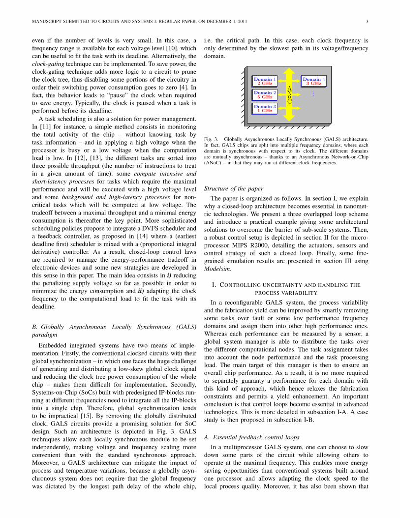
Embedded integrated systems have two means of imple-mentation. Firstly, the conventional clocked circuits with theirglobal synchronization – in which one faces the huge challengeof generating and distributing a low-skew global clock signaland reducing the clock tree power consumption of the wholechip – makes them difficult for implementation. Secondly,Systems-on-Chip (SoCs) built with predesigned IP-blocks run-ning at different frequencies need to integrate all the IP-blocksinto a single chip. Therefore, global synchronization tendsto be impractical [15]. By removing the globally distributedclock, GALS circuits provide a promising solution for SoCdesign. Such an architecture is depicted in Fig. 3. GALStechniques allow each locally synchronous module to be setindependently, making voltage and frequency scaling moreconvenient than with the standard synchronous approach.Moreover, a GALS architecture can mitigate the impact ofprocess and temperature variations, because a globally asyn-chronous system does not require that the global frequencywas dictated by the longest path delay of the whole chip,
i.e. the critical path. In this case, each clock frequency isonly determined by the slowest path in its voltage/frequencydomain.
Domain 12 GHz
5 GHz
1 GHz
3 GHzANoC
Domain 3
Domain 4
Domain 2
Fig. 3. Globally Asynchronous Locally Synchronous (GALS) architecture.In fact, GALS chips are split into multiple frequency domains, where eachdomain is synchronous with respect to its clock. The different domainsare mutually asynchronous – thanks to an Asynchronous Network-on-Chip(ANoC) – in that they may run at different clock frequencies.
Structure of the paper
The paper is organized as follows. In section I, we explainwhy a closed-loop architecture becomes essential in nanomet-ric technologies. We present a three overlapped loop schemeand introduce a practical example giving some architecturalsolutions to overcome the barrier of sub-scale systems. Then,a robust control setup is depicted in section II for the micro-processor MIPS R2000, detailing the actuators, sensors andcontrol strategy of such a closed loop. Finally, some fine-grained simulation results are presented in section III usingModelsim.
I. CONTROLLING UNCERTAINTY AND HANDLING THEPROCESS VARIABILITY
In a reconfigurable GALS system, the process variabilityand the fabrication yield can be improved by smartly removingsome tasks over fault or some low performance frequencydomains and assign them into other high performance ones.Whereas each performance can be measured by a sensor, aglobal system manager is able to distribute the tasks overthe different computational nodes. The task assignment takesinto account the node performance and the task processingload. The main target of this manager is then to ensure anoverall chip performance. As a result, it is no more requiredto separately guaranty a performance for each domain withthis kind of approach, which hence relaxes the fabricationconstraints and permits a yield enhancement. An importantconclusion is that control loops become essential in advancedtechnologies. This is more detailed in subsection I-A. A casestudy is then proposed in subsection I-B.
A. Essential feedback control loops
In a multiprocessor GALS system, one can choose to slowdown some parts of the circuit while allowing others tooperate at the maximal frequency. This enables more energysaving opportunities than conventional systems built aroundone processor and allows adapting the clock speed to thelocal process quality. Moreover, it has also been shown that

MANUSCRIPT SUBMITTED TO CIRCUITS AND SYSTEMS I: REGULAR PAPER, ON DECEMBER 1, 2011 4
multiple-clock designs with voltage scaling are even betternot only in terms of power and performance, but also interms of variability [16]. As a result, building a systembased on the implementation of hardware resources whoseperformance are unpredictable at the fabrication time requiresto have some global management strategies, adapting thevoltage/frequency in order to respect real-time constraints ofthe application and the allocated energy budget. Therefore, itis proposed to use automatic feedback loops based on i) themeasurement of the real local performance and the actuationof the voltage/frequency variables (hardware level) as well asii) the suitable hardware resource allocation for the executionof a task in the assigned time/energy budget (operating systemlevel). Then, the idea is the use of DVFS techniques withtask scheduling to dynamically manage not only the energybudget but also the activity of the processing nodes. Someadvanced control strategies will allow an optimal regulation ofthe frequency/voltage converter according to the computationalload and the load distribution in the various GALS processors.Furthermore, in order to compensate for the process variationdue to the technology dispersion, and optimize the operationof the circuit, the dynamic voltage/frequency regulation shouldbe self-adjustable with variable loads and dispersion modelsand robust against process variability.
One of the main points of interest of the proposal is tohandle the uncertainty of a processing node over a GALSsystem and also to reduce its energy consumption by means ofautomatic control methods. Activity sensors are supposed tobe embedded in each processing unit. These sensors providea real performance measurement of different processing nodesafter the fabrication process, which will be used afterwards bythe operating system to distribute tasks over different nodes.This means the need for the rescheduling of tasks in eachprocessing node to meet the new assigned deadlines, and thiswill be achieved by controlling its voltage/frequency, which inaccordance will control its consumption of energy. The controlsystem is based on three overlapped control loops, applied indifferent architecture levels, which are depicted in Fig. 4:
1) Control of the processing power (supply voltage andclock frequency).
2) Control of the tradeoff between energy consumption andcomputational performance.
3) Control of the quality of the running application.
Voltage, frequency and energy control loops are used in orderto adapt the energy consumption and the process variabilityeffect. The other loop is needed to deal with the Quality ofService (QoS) at the application level, with the limitation ofprocessing power and/or channel of communication and withsome constraints in energy consumption. This latter loop alsomanages the different domains of the chip (denoted cluster inFig. 4) with their own performance.
The different control loops are nested. Actually, the op-erating system (or the high-level loop) provides a set ofinformation – required computational speed, in terms of num-ber of instructions and deadlines for each task to treat –which can be statically inserted into the code or dynamicallycomputed at run time by the OS. These information about
fclk
ω
ComputationalNodes
Vdd
flevel
Vlevel
ωsp − ω
ωsp
FrequencyController
VoltageController
Energy/PerformanceController
Cluster
λsp
λ
λsp − λ QoS Controller
Fig. 4. Automatic control are essential in nanometric chips to manage thecomputational activity and energy consumption. Three overlapped loops arehence introduced: the voltage and frequency control (low-level), the energy-performance tradeoff control (middle-level) and the applicative quality ofservice control (high-level).
the real-time requirements of the applications enable to createa computational load profile with respect to time. Thereare also sensors embedded in each processing unit in orderto provide real-time measurements of the processor speed.Consequently, combining such a profile with such a monitoringmakes possible to apply a fine-grain power/energy manage-ment allowing application deadlines to be met. The DVFShardware part (or low-level loop) contains voltage/frequencyconverters, such as a DC-DC converter and a programmableclock generator. Then, a controller (the one from the middle-level loop) dynamically controls these power actuators toscale the supply voltage as well as the clock frequency, inorder to satisfy the application computational needs with anappropriate management strategy. Of course, this controllershould have a strong robustness against process variabilityfor a correct system behavior. These solutions – the threeoverlapped feedback control loops with some specific sensorsto monitor the activity of the chip – were established withinthe ARAVIS project context which is now introduced.
B. Case study overview: the ARAVIS project
Using both a Network-on-Chip (NoC) distributed communi-cation scheme and a GALS approach offers an easy integrationof different functional units thanks to a local clock generation[17]. Moreover, it allows better energy savings since eachfunctional unit can easily have its own independent clockfrequency and voltage. Hence, such an architecture appearsas natural enablers for distributed power management systemsas well as for local DVFS. A detailed block diagram formodeling DVFS and local process quality management in aGALS system is shown in Fig. 5. This practical exampleis part of the ARAVIS project which aims at providingarchitectural solutions for manufacturing circuits in nanometrictechnologies with strong technological uncertainties.
Since in advanced technologies, the associated processorleakage has an important contribution to the system energyconsumption, a sleep mode management block is used toput useless processors into a sleep mode in order to limit

MANUSCRIPT SUBMITTED TO CIRCUITS AND SYSTEMS I: REGULAR PAPER, ON DECEMBER 1, 2011 5
Fig. 5. Energy-performance management architecture proposed in theARAVIS project to control a multi-processor system with high processvariability.
their static power consumption. On the other hand, somespeed sensors are used to calculate the real-time computationalspeed of the processing units (in Million of Instructions PerSecond for instance). Activity monitors disseminated into eachvoltage-frequency island are also used to locally evaluatethe process quality in terms of its relative speed with re-spect to the other processing nodes (denoted intrinsic speed).The intrinsic speed value defines the upper clock frequencybound of the operating voltage-frequency island. There arealso two actuators: the DC-DC converter which providesthe supply voltage and the programmable asynchronous ringwhich generates the desired clock frequency to each localprocessing node. Finally, the digital controller manages thevoltage/frequency couple. It processes the error between theunit speed and the speed setpoint information extracted fromthe information sent by the operating system (in terms ofnumber of instructions and deadlines) within a closed-loopsystem, and by applying a well-suited compensator sends thedesired voltage and frequency code values to the actuators.Consequently, the system is able to locally adapt their outputvoltage and clock frequency values clock domain by clockdomain, in order to limit their dynamic power consumption.Furthermore, the Asynchronous NoC (ANoC) is the reliablecommunication path between the different domains. In thismodel, we propose that data communications between twodifferent processing nodes can fix the speed to the slowestcommunicating node. This is done by a local synchronizationmechanism which is based on handshakes. Thus, the slowestcommunicating node of the ANoC fixes the throughput inorder to have a secure communication without metastabilityproblem and an adaptation to process variability too [18].
II. ROBUST CONTROL DESIGN TO PROCESS VARIABILITY:APPLICATION TO THE MIPS R2000
MIPS R2000 is a 32-bit Reduced Instruction Set Computer(RISC) initially developed by the Stanford University. It standsfor a Microprocessor without Interlocked Pipeline Stages. This
means that it has single execution cycle instructions so that thecompiler can schedule them to avoid conflicts. The MIPS ar-chitecture includes thirty-two general-purpose 32-bit registersand fifty-eight instructions, each 32 bits long. The instructionsare processed in a five-stage pipeline: fetch, decode, execute,memory, and write back. MIPS R2000 also includes a copro-cessor to handle exceptions and hold configuration bits. Onlyfew configuration bits are used in the R2000 architecture, andare mostly used to enable/disable exceptions and to configurethe caches. The MIPS architecture supports exception handlingand interrupts. Due to the MIPS R2000 simplicity in terms ofarchitecture, programming model and instruction set, as wellas availability as an open core, it has been used as our maincase of study in the DVFS control system design for a GALS-NoC, that compensate for the CMOS uncertainties in nanomet-ric technologies (STMicroelectronics 45nm technology in thepresent case). The MIPS R2000 is used as a processing node inthe energy-performance management architecture previouslyintroduced in Fig. 5. Finally, the integration of the MIPSR2000 is depicted in Fig. 6. The actuators (programmableoscillator and Vdd-hopping), the speed sensor and the digitalcontroller required for a robust control to process variabilityare then detailed in the following subsections. On the otherhand, the ROM memory is loaded with a factorial program totest its execution by the processor. Details of the MIPS R2000synthesis and analysis results will be shown in section III.
Fig. 6. Architecture of the controlled system in the MIPS environment. Thedigital controller calculates the voltage and frequency levels to send to theVdd-hopping and the programmable oscillator in order to manage the energy-performance tradeoff of the MIPS R2000. A speed sensor is also used toprovide the real-time computational speed.
A. Vdd-hopping to scale voltage
The DC-DC converter is a circuit that converts a voltagesource (of direct current) from one voltage level to another.Two kinds of DC-DC converter can be used. The first classis a continuous DC-DC converter which provides an accuratesupply voltage, but with a weak efficiency. The second kind ofconverter is a digitally controlled step-converter (Vdd-hoppingconverter) which has a better efficiency but discrete outputvalues. Such a mechanism was described in [19], where twovoltages Vlow or Vhigh could supply the chip. In that case,

MANUSCRIPT SUBMITTED TO CIRCUITS AND SYSTEMS I: REGULAR PAPER, ON DECEMBER 1, 2011 6
the system simply goes to low or high voltage when the inputsignal becomes Vlevel = Vlevel low or Vlevel = Vlevel highrespectively, with a given transition time and dynamics thatdepend upon an internal control law (one could refer to thereference above for more details). The Vdd-hopping techniqueis also modeled with two possible voltage levels in the presentpaper. Eventually, considering that this inner-loop is extremelyfast with respect to the loop considered in this paper, one canneglect the dynamics of the Vdd-hopping.
B. Programmable self-timed ring to scale frequency and man-age variations
The application of the proposed DVFS to a system requiresthe use of a process variability robust source for generatingadjustable clocks. For example, these clocks can be derivedfrom analog Voltage Controlled Oscillators (VCO), whichare a part of a Phase Locked Loop (PLL). However, VCOshave a limited operating range and require a stabilizationtime when changing the frequency [20]. Another solutionis to use a standard clock divider, but this will make thetime resolution coarser due to counting integer periods ofthe input frequency [21]. In addition, they give regular timestep which implies irregular frequency step (usually frequencystep follows “1/x” curve). Today many studies are oriented toSelf-Timed Ring (STR) oscillators which present well-suitedcharacteristics for managing process variability and offering anappropriate structure to limit the phase noise. Therefore, theyare considered as a promising solution for generating clockseven in presence of process variability. In [22], [23], theyare efficiently used to generate high-resolution timing signals.Their robustness against process variability in comparison toinverter rings is proven in [24]. Moreover, self-timed ringscan easily be configured to change their frequency by justcontrolling their initialization at reset time. At the opposite,inverter rings are not programmable.
Whereas the background, definitions and principles of theProgrammable Self-Timed Ring (PSTR) are detailed next,a simple model based on the behavior of the fully pro-grammable/stoppable oscillator of [25] is firstly given. Sucha frequency controller has a linear variation of its outputfrequency with respect to the digital controller feed value. Thisdigital controller value defines the operating frequency. Thefrequency controller also changes its output frequency withrespect to the input voltage, as shown in Fig. 7. The resultingmodel is fclk = γfVdd, where γ is a constant while the desiredfrequency f depends on the input signal, i.e. f = ψ(flevel),using such a look-up table mechanism for instance. Thisasynchronous ring was modeled in Matlab/Simulink and testedunder the two specified voltage levels of the DC-DC converterfor 45nm CMOS technology. In fact, only some limitedfrequency values are possible, that is flevel = flevel n withn ∈ 1, 2, . . . , N and fn > fn+1, and switching from onefrequency to another can be considered as instantaneous.
1) Self-timed rings: The C-element is the basic element inasynchronous circuit design, introduced by D. E. Muller [26].The C-elements set their output to the input values if theirinputs are equal and hold their output otherwise. In Fig. 8(a),
Fig. 7. Behavioral variation of the frequency controller with respect to theinput voltage values.
a possible CMOS implementation is showed where the initial-ization circuit is omitted. Each stage of a STR is composedof a C-element and an inverter connected to one of its inputs.The input which is connected to the previous stage is markedF (Forward) and the input which is connected to the followingstage is marked R (Reverse), C denotes the output of the stage,as shown in Fig. 8(b).
(a) Muller C-element.
(b) Self-timed ring.
Fig. 8. Representation of a possible CMOS implementation of a self-timedring, whose each stage is composed of a C-element and an inverter.
The behavior of the STR is mainly based on the tokens “T”and bubbles “B” propagation rule. Stagei contains a token ifits output Ci is not equal to the output Ci+1 of Stagei+1.On the other hand, Stagei contains a bubble if its outputCi is equal to the output Ci+1 of Stagei+1. The numberof tokens and bubbles will be respectively denoted NT andNB , with NT + NB = N , where N is the number of thering stages. For keeping the ring oscillating, NT must be aneven number. The reader can think about this as the dualityof designing the inverter ring by odd number of stages. Eachstage of the STR contains either a token or a bubble. If a tokenis present in a Stagei, it will propagate to Stagei+1 if andonly if Stagei+1 contains a bubble. The bubble of Stagei+1
will move backward to Stagei. This implies a transition

MANUSCRIPT SUBMITTED TO CIRCUITS AND SYSTEMS I: REGULAR PAPER, ON DECEMBER 1, 2011 7
on Stagei+1 output. For instance, hereafter is depicted thetoken/bubble movements in a five stage STR which containsfour tokens and one bubble.
Example: TTBTT (01001) ⇒ TBTTT (01101) ⇒ BTTTT(00101) ⇒ TTTTB (10101) ⇒ TTTBT (10100) ⇒ TTBTT(01001)
2) Programmable self-timed rings: The oscillation fre-quency in STRs depends on the initialization (number oftokens and bubbles and hence the corresponding number ofstages). The oscillation frequency in a self-timed ring can beapproximated according to the number of tokens and bubblesby the formula from [27], which is
Fosc STR =1
2D(R+ 1)
(D,R) =
(Drr, NT/NB) if Dff/Drr ≥ NT/NB
(Dff , NB/NT ) if Dff/Drr < NT/NB
where Dff is the static forward propagation delay from inputF to output C and Drr is the static reverse propagation delayfrom input R to output C.
Programmability can be simply introduced to STRs bycontrolling the tokens/bubbles ratio and the number of STRstages. Programmable Self-Timed Ring (PSTR) was presentedfor the first time in [25]. It uses STR stages based on Mullergates which have a set/reset control to dynamically inserttokens and bubbles into each STR stage. Moreover, to be ableto change the number of stages, a multiplexer is placed aftereach stage. The idea presented in [25] was also extended tohave a fully Programmable/Stoppable Oscillator (PSO) basedon the PSTR. Look-up tables loaded with the initializationtoken control word (i.e. to control NT/NB), and the stagecontrol word (i.e. to control N ) was used to program the PSTRwith a chosen set of frequencies.
3) PSTR programmability applied to MIPS R2000:Presently, the variability is captured in the design by usingsimulation corners, which correspond to the values of certainprocess parameters that deviate by a certain ratio from theirtypical value. In the STMicroelectronics 45nm CMOS tech-nology, three PVT (Process, Voltage, and Temperature) cornersare available, denoted Best, Nominal and Worst. All standardlogic cells were characterized at each of these three corners.So, we use Synopsis Design Vision tool to implement a GALS-NoC island based on a MIPS-R2000 using STMicroelectronics45nm CMOS libraries in order to test its behavior at each ofthe previously specified PVT corners. Since, our main goal isto define the optimal operating clock frequency needed by theprocessing load that compensates for the propagation delayvariations due to the process variability impact. Therefore,the critical path delay of the synthesized MIPS R2000 withrespect to the supply voltage is analyzed at the three differentPVT corners. According to the STMicroelectronics 45nmlibraries, we choose Vlow = 0.95 volts and Vhigh = 1.1 volts.Consequently, the optimal clock frequency needed by theMIPS R2000 at the specified two voltage levels with the threedifferent process variability corners are defined as shown inTable I.
In order to adapt the generated clock frequency with respectto the current located process variability impact and to the
TABLE IMIPS R2000 OPTIMAL CLOCK FREQUENCIES REQUIRED TO COMPENSATE
FOR THE PROCESS VARIABILITY IMPACT ON THE 45 nm CMOSTECHNOLOGY.
Voltage level Clock frequency (MHz)(V) for different process variability conditions
Worst Nominal Best0.95 60 75 851.1 95 115 145
processed workload, activity sensors are required. As alreadyexplained in section I, they play a critical role in DVFSsystems and must be carefully selected. The period of thereference clock is crucial since it determines the accuracyof the calculated average speed. Moreover, it determines thesystem speed response. In fact, the speed sensor integratesalso a register to memorize the computational speed on apredefined period and determines the average speed on eachrising-edge of the reference clock (i.e. RST signal in Fig. 6).If this period is short, the system will be fast but the calculatedaverage speed will not be accurate. On the opposite, a longperiod leads to a slow system but to a more accurate speed.Therefore, according to the set of clock frequencies availablefor the MIPS R2000, the reference clock frequency was chosento be 2 MHz, in order to count a considerable amount ofinstructions with a proper system response. To conclude, thecomputational speed is now applied in terms of number ofinstructions executed per 500ns to the digital controller.
Whereas three defined process variability corners are de-fined in the 45nm CMOS libraries provided by STMicro-electronics, the contents of the PSO code memory presentedin [25] are split into three main pages. Based upon theactivity monitor output, the corresponding page will be se-lected. Each page contains a set of programming codes thatgenerates the suitable clock frequencies for the MIPS R2000which compensate for the delay variation due to the processvariability effects. In each programming code set, we haveone code corresponding to the clock frequency Fhigh at thehigh voltage Vhigh, and two other codes corresponding to theclock frequencies Flow1 and Flow2 at the low voltage Vlow (adiscussion on the number of frequency levels to use follows insubsection II-C). Consequently, our programmable oscillatorcan be simply represented by the block diagram shown inFig. 9. Note that FC is the new frequency code which is sentby the digital controller with the activity monitor evaluation ofthe process variability to the PSO. CF is the change frequencypulse that indicates the presence of a new frequency code andPC is the pause clock pulse to stop the oscillator, refer to [25].PCW is the PSTR programming code word that specifies thering initialization and its corresponding number of stages.
C. Control of the energy-performance tradeoff with strongprocess variability robustness
The digital controller introduced in Fig. 5 is upstream fromthe Vdd-hopping and the asynchronous ring since it calculatesthe voltage and frequency level values that have to be sentto these actuators in order to minimize the energy consump-tion while guaranteeing good computational performance. The

MANUSCRIPT SUBMITTED TO CIRCUITS AND SYSTEMS I: REGULAR PAPER, ON DECEMBER 1, 2011 8
Fig. 9. Memory mapping of the programmable oscillator. It selects the PSTRprogramming code to apply in function of a given frequency level calculatedby the digital controller.
resulting system architecture from a control point of viewis given in Fig. 10, where the device denotes the electronicsystem to control (a processor or a computational node forexample, or the MIPS R2000 in the present case). A dynamicscaling of the supply power – and therefore the energyconsumption – is possible introducing a closed-loop controllerwhich monitors the activity of the device (its computationalspeed ω in number of instructions per second) in order to adaptthe control variables with respect to a given computationalload ref to treat. Finally, the model of the whole controlledsystem (the device and the two actuators) can be approximatedby an affine function [28], that is
ω = σfVdd (2)
where σ is an unknown parameter which, in fact, can beidentified but highly varies with temperature and location onthe chip (variability). Nevertheless, the dynamics introducedby the control law will make possible to control the systemwithout any information on this parameter.
ω
ω
ref
flevel
VlevelVdd
fclk
System
ControllerVdd
hopping
Oscillator Device
Vdd
Fig. 10. Representation of the system architecture to control the energy-performance tradeoff. The controller calculates the control variables (voltagelevel Vlevel and frequency level flevel) from the error between the measuredcomputational speed ω and a given setpoint ref , and sends them to bothactuators (the Vdd-hopping and the ring oscillator respectively).
Actually, the control of the energy-performance tradeoff ina voltage scalable device consists in minimizing the energyconsumption (reducing as much as possible the supply voltage)while ensuring some good computational performance (fittingthe tasks with their deadline). This is why we propose todynamically calculate an energy-efficient computational speedsetpoint that the system will then have to track. This setpointis based on some information provided by a higher level (theoperating system for example) for each task Ti to treat, thatare the computational load – i.e. the number of instructions
Ωi to execute – and the deadline ∆i. Moreover, let Λi denotethe laxity, that is the remaining available time to complete agiven task. Note that these parameters can change during therunning time of a task (if the OS decides to update them forinstance), this is why they are time-dependant.
The presence of deadline and time horizon to computetasks naturally leads to predictive control. Predictive controlconsists in finding an open-loop control profile over sometime horizons and in applying it until the next time instant.The control problem is then reconsidered using the new statevariables and a new control profile is generated. This finallyyields a closed-loop control and the stability relies in the waythe open-loop control is chosen. The horizon can be constant,infinite or less classically contractive as in the present paper.The key point is the choice of the open-loop strategy andits computational cost. Indeed, if predictive control is knownto be a robust approach, it is also often associated to highcomputational cost which is not acceptable in the presentcase. Whereas the classical strategy consists in minimizingsome cost functions, the strategy adopted here is called fastpredictive control and consists in taking advantage of thestructure of the dynamical system to fasten the finding ofthe open-loop control [29]. The simplicity of system (2)considered here is very suitable for such strategies. The mainidea of the predictive strategy is firstly intuitively explainedand its formal expression is given in the sequel.
1) Speed setpoint building: Let ωmax denote the maximalcomputational speed when the system is running at highvoltage, that is ωmax = σFVhighmaxVhigh from (2), whereFVhighmax is the maximal frequency in the available rangeat Vhigh. Respectively, let ωmax denote the maximal possiblespeed at low voltage, that is ωmax = σFVlowmaxVlow, whereFVlowmax is the maximal frequency at Vlow. It follows thatthe high voltage level is necessary as soon as the averagespeed setpoint of a task is higher than ωmax in order tonot miss a given deadline. An intuitive method consists inbuilding the average speed setpoint of each task – that is theratio Ωi/∆i – in such a way that the number of instructionsto do is performed at the end of the task. This is depicted inFig. 11(a). However, this method is not energy-efficient sincea whole task can be computed with the penalizing high supplyvoltage, such as highlighted by tVhigh
for task T2. Moreover,this technique implies to have an infinite number of voltagelevels. Nevertheless, a suggested solution consists in splittingthe tasks into two parts. This is represented in Fig. 11(b).Firstly, the chip begins to run at high voltage – if required –with the maximal available frequency in order to achieve themaximal possible speed ωmax to go faster than the averagespeed, such as for T2 from time t2 to k. Then, the task could befinished at low voltage – which, consequently, highly reducesthe energy consumption – with a speed lower than ωmax. Akey point in this strategy is that the switching time to go fromVhigh to Vlow has to be suitably calculated in order to ensuresome good computational performance. However, k is not apriori known and, therefore, a predictive control law has to beused to dynamically calculate this switching time.
In fact, the lower is the supply voltage the better will bereduced the energy consumption since the supply voltage is the

MANUSCRIPT SUBMITTED TO CIRCUITS AND SYSTEMS I: REGULAR PAPER, ON DECEMBER 1, 2011 9
average computational speed setpoint ωsp(t)
tVhigh
voltage
time
Ω2∆2
Ω1∆1
Ω3∆3 T3
T2
T1
ωmax
ωmax
t2 t3 timet1
Vhigh
Vlow
t2 t3t1
(a) Intuitive average speed setpoint.
energy-efficient computational speed setpoint ωsp(t)
time
voltage
Vhigh
Vlow
time
tVhigh
t2 t3
Ω2∆2
Ω1∆1
Ω3∆3 T3
T2
T1
ωmax
ωmax
t2 t3kt1
t1 k
(b) Energy-efficient speed setpoint.
Fig. 11. Different computational speed setpoint buildings can be used tosave energy consumption while ensuring some good performance.
penalizing parameter in DVFS. For this reason, we proposeto have only one possible frequency Fhigh (i.e. FVhighmax)when running at Vhigh and so minimize the penalizing highvoltage running time. On the other hand, several frequencylevels Flown
are possible at the low voltage level Vlow because,as the energy consumption could not be reduced anymore –since no lower voltage level exists – the degree of freedom onthe frequency will allow to fit the task with its deadline (asmuch as this is possible). In the following, we propose to usetwo frequency levels at Vlow and we decide that the maximalone is Flow1 = FVlowmax. Whereas the maximal levels Fhighand Flow1 are determined from the optimal frequency valuesin Table I (regarding the variability of the chip), one couldnote that the second frequency level at low voltage, i.e. Flow2 ,is equal to Flow1/2, which enables to have 3 dB reduction inthe power consumption. Note that Flow2 is included to addmore power saving opportunities to our DVFS once possible.
2) Fast predictive control: Actually, the predictive issuecan be formulated as an optimization problem. For eachtask Ti to treat, what is the computational speed setpointwhich minimizes the high voltage running time tVhigh
whileguaranteeing that the executed instruction number is equal tothe number of instructions to do, that is
min tVhighs.t.
∫
∆i(t)
ω(t) dt = Ωi(t)
where∫ωdt corresponds to the executed number of instruc-
tions for the current task. This optimal criteria allows to solvethe predictive problem but is too complex to be implemented inan integrated controller with low resources, as in the presentcase. Nevertheless, the closed-loop solution yields an easierand faster algorithm since, in fact, one simply needs to knowi) the computational load to treat and ii) how much time isavailable to do it. The remaining time before the end of thetask is hence necessary, this is why the laxity Λi will beused next instead of the deadline ∆i. The speed required tofit the task with its deadline regarding what it has alreadybeen executed – afterwards denoted the predicted speed δ –is dynamically calculated at each sampling instant as follows
δ(tk+1) =Ωi(tk)−
∑tk−τi
τiω(tk)
Λi(tk)(3)
where τi is the beginning of the task Ti, tk and tk+1 are thecurrent and next sampling time respectively. The implementa-tion of the previous equation then becomes
Ω(tk) = Ω(tk−1) + Tsω(tk)
δ(tk+1) =Ωi(tk)− Ω(tk)
Λi(tk)(4)
where Ω is the integration of the computational speed ω, Tsis the sampling period and tk−1 is the last sampling time.Furthermore, a conditional instruction is added to be coherentwith (3). Indeed, as the real-time speed is integrated on therunning time of each task, the variable Ω has to be reset whena task is executed, which means in the last sampling timebefore its deadline. More precisely, it is not set to zero toprevent the case when the task is not completely executed atits deadline but it is adjusted with the difference between whatit has already been done and what it was required to do, suchthat
Ω(tk) = Ω(tk)− Ωi(tk) if Λi(tk) ≤ Ts
The energy-efficient speed setpoint ωsp is then directly de-duced from the value of the predicted speed, and so are thevoltage and frequency levels. Indeed, the system has to runat Vhigh and Fhigh when the required setpoint is ωmax, elsethe low voltage will be enough to finish the task. In fact thecomputational speed setpoint is not really required since thecontrol variables are easily deduced, but we notice it anyway(for a well understanding) in the control decisions, that are
∣∣∣∣∣∣
ωsp(tk+1) = ωmax
Vlevel(tk+1) = Vhighflevel(tk+1) = fhigh
if δ(tk+1) > ωmax
∣∣∣∣∣∣
ωsp(tk+1) = ωmaxVlevel(tk+1) = Vlowflevel(tk+1) = flown
otherwise
where a frequency control strategy is needed to determine thefrequency level flown
. However, the principle is not detailedhere since it remains the same than for the voltage decision.Also, one could note that the division in (4) could be removedfor a practical implementation, simply replacing the conditionδ(tk+1) > ωmax in the previous control decision by Ωi(tk)−

MANUSCRIPT SUBMITTED TO CIRCUITS AND SYSTEMS I: REGULAR PAPER, ON DECEMBER 1, 2011 10
Ω(tk) > ωmax ·Λi(tk). At the end, the algorithm of the digitalcontroller is hence quite easy to implement in a circuit withlimited resources.
The performance are guaranteed because the execution of atask always starts with the penalizing high voltage level – byconstruction of the predictive control law – and the low onewill not be applied while the remaining computational load isimportant (higher than the maximal possible speed at Vlow).As a result, it is not possible to make better. Furthermore,even if the voltage/frequency levels discretely vary, the speedsetpoint to track is always higher or equal than required byconstruction. On the other hand, the Lyapunov stability isbased on an elementary physical constatation: if the totalenergy of the system tends to continuously decline, then thissystem is stable since it is going to an equilibrium state.Let V = xTPx be a candidate Lyapunov function, withP positive definite and x(tk) = Ωi(tk) − Ω(tk). This latterexpression comes from (4), where x refers to the remainingload in the contractive time horizon of the task. Therefore, theLyapunov function intuitively decreases – because the speedof the processor can only be positive – and so is ensured thestability of a task.
3) Estimation of the maximal speeds: The maximal speedsωmax and ωmax might be obtained from the equation of thesystem model (2). They are proportional to the voltage and themaximal frequency for each voltage level. However, even if theproportional gain is inherent to the device it could vary withtemperature or location (variability), and yet, the control lawhas to be robust to such an uncertainty. Furthermore, the valueof the different parameters are not known. For these reasons,we propose to estimate the maximal speeds. Let ωm denote theestimated speeds where m denotes the different power modes.A solution consists in measuring the system speed for eachcouple voltage/frequency levels. Moreover, we propose to usea weighted average of the measured speed in order to filterthe (possible) fluctuations of the measurement, which yields
ifVlevel(tk−1) = Vmflevel(tk−1) = fm
ωm(tk) = (1− ρ)ωm(tk−1) + ρω(tk)
where 0 ≤ ρ ≤ 1 is the weighted value. Furthermore, theproposed estimation of the computational speeds – whichleads to a control law without any information on the systemparameters – yields a robust strategy which will self-adaptwhenever the performance of the controlled chip. This is veryimportant for process variability (see [28] for further detailson how to bound ρ to satisfy such a robustness).
4) Clock-gating principle: On top of the proposed strategy,a last control decision is also possible “deactivating” the clockof the device. This is called the clock-gating principle, asexplained in introduction. In this case, the processor runs withthe low voltage and a null frequency. This behavior is usefulwhen a task is performed before its deadline to pause the clockuntil the beginning of the following one. However, in order tominimize the using of the clock-gating principle, we decideto make available this principle only if the beginning of thefollowing task is not too close, that is when Λi(tk) > Λmin,where Λmin is a tunable parameter.
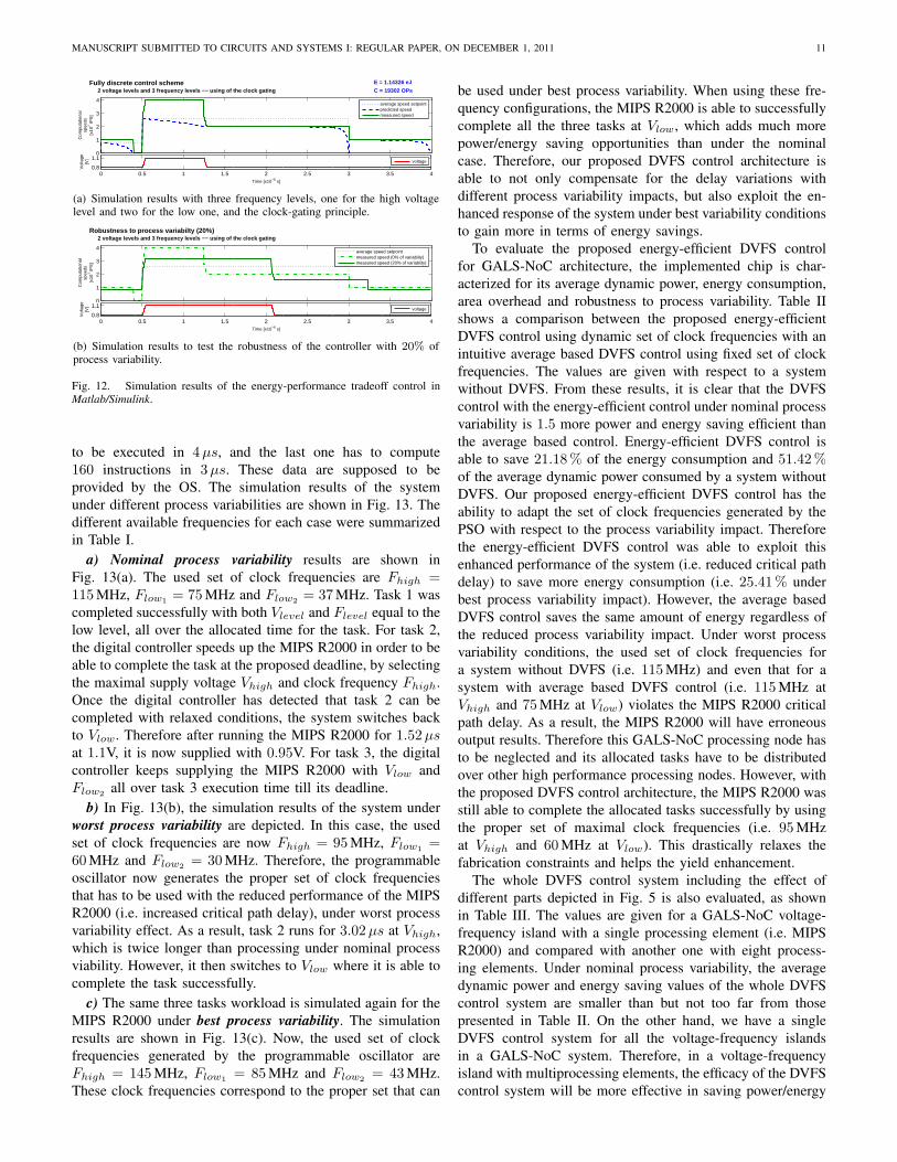
5) Coarse-grain simulation results: Some initial simulationresults are realized in Matlab/Simulink in order to evaluate theefficiency of the proposed digital controller. A scenario withthree tasks to execute is proposed: the first task starts with4 instructions to do in 0.5µs, then a 65 instruction task hasto be executed in 2.5µs and the last one has to compute 10instructions in 1µs. These data are considered as provided bythe OS. Fig. 12(a) shows the simulation results of the systemwith two voltage levels and three frequency levels. The top plotshows the average speed setpoint of each task (for guideline),the predicted speed (for guideline) and the measured computa-tional speed, while the bottom plot shows the supply voltage.The energy consumption is calculated in order to have an ideaof the achieved reduction. The control strategy is comparedwith a system without DVFS mechanism – where the supplyvoltage is fixed to the most penalizing level, i.e. Vdd = Vhigh,and so is the clock frequency fclk = Fhigh – and without DVSmechanism where only the frequency can be scaled. Fig. 12(a)shows that with the two possible voltage levels the systemruns during about 80 % of the simulation time at low voltage.As a result, a reduction of about 30 % and 65 % of the energyconsumption is achieved (in comparison with a system withoutDVS and DVFS mechanism respectively) with the three-tasktest bench proposed. One could refer to [28] for further details.
As the proposed control strategy does not use any infor-mation on the system parameters, the controller adapts itselfwith these uncertainties. Fig. 12(b) shows how the system isstill working for 20 % of process variability effects, that iswhen the real performance of the circuit are 20 % less thanexpected. One could see that the estimation of the maximalcomputational speed allows the system to still work, even ifthe processing node does not work as expected. Of course,in order to compensate a lower computational speed inducedby the process variability, the system will run a longer timeat the penalizing supply voltage. Note that the robustness islimited by the maximal possible activity of the processing nodeanyway. Indeed, if the chip is not enough fast to computethe task while running at the maximal speed (the chip runswith the highest voltage and highest frequency), the controllerwould not be able to do anything to solve this failure. Theonly way is to migrate the task allocated to this processingnode to a higher performance one, and this has to be done bythe operating system. More fine-grain simulation results areshown in section III for the whole MIPS-R2000 architecturewith the 45nm CMOS parameter variations.
III. SIMULATION RESULTS
The design presented in section II is implemented usingSTMicroelectronics 45nm CMOS standard libraries for thephysical implementation [30]. The digital controller mainprinciple of operation is based on implementing the energy-efficient control algorithm, described in subsection II-C. Inorder to evaluate the efficiency of the proposed control strategyunder different process variability conditions, a post layoutsimulation with Modelsim has been performed. A scenariowith three tasks is proposed: the first task starts with 100instructions to do in 2µs, then a 340 instruction task has
MANUSCRIPT SUBMITTED TO CIRCUITS AND SYSTEMS I: REGULAR PAPER, ON DECEMBER 1, 2011 11
Com
puta
tiona
lsp
eeds
[x10
7 IPS
]
0
1
2
3
4average speed setpointpredicted speedmeasured speed
Vol
tage
[V]
Time [x10−6 s]
0 0.5 1 1.5 2 2.5 3 3.5 40.8
1.1voltage
Fully discrete control scheme2 voltage levels and 3 frequency levels −− using of the clock gating
E = 1.14326 eJ
C = 19302 OPs
(a) Simulation results with three frequency levels, one for the high voltagelevel and two for the low one, and the clock-gating principle.
Com
puta
tiona
lsp
eeds
[x10
7 IPS
]
0
1
2
3
4average speed setpointmeasured speed (0% of variabiity)measured speed (20% of variabiity)
Vol
tage
[V]
Time [x10−6 s]
0 0.5 1 1.5 2 2.5 3 3.5 40.8
1.1voltage
Robustness to process variabilty (20%)2 voltage levels and 3 frequency levels −− using of the clock gating
(b) Simulation results to test the robustness of the controller with 20% ofprocess variability.
Fig. 12. Simulation results of the energy-performance tradeoff control inMatlab/Simulink.
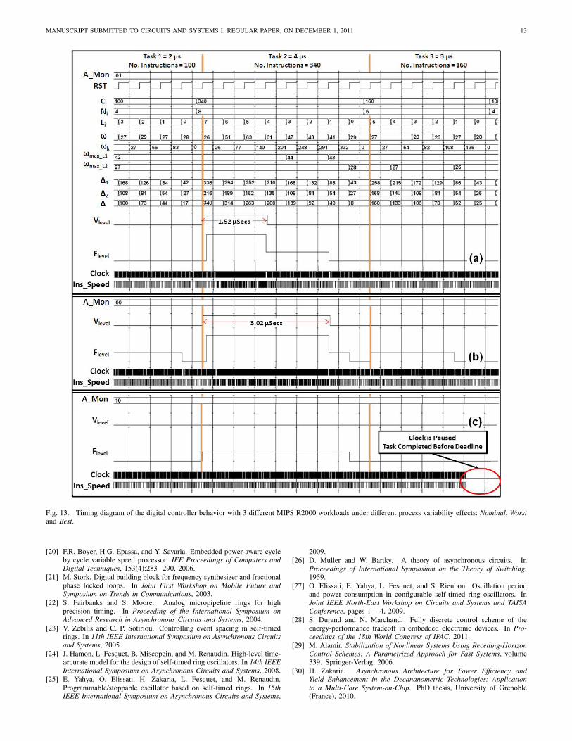
to be executed in 4µs, and the last one has to compute160 instructions in 3µs. These data are supposed to beprovided by the OS. The simulation results of the systemunder different process variabilities are shown in Fig. 13. Thedifferent available frequencies for each case were summarizedin Table I.
a) Nominal process variability results are shown inFig. 13(a). The used set of clock frequencies are Fhigh =115 MHz, Flow1 = 75 MHz and Flow2 = 37 MHz. Task 1 wascompleted successfully with both Vlevel and Flevel equal to thelow level, all over the allocated time for the task. For task 2,the digital controller speeds up the MIPS R2000 in order to beable to complete the task at the proposed deadline, by selectingthe maximal supply voltage Vhigh and clock frequency Fhigh.Once the digital controller has detected that task 2 can becompleted with relaxed conditions, the system switches backto Vlow. Therefore after running the MIPS R2000 for 1.52µsat 1.1V, it is now supplied with 0.95V. For task 3, the digitalcontroller keeps supplying the MIPS R2000 with Vlow andFlow2 all over task 3 execution time till its deadline.
b) In Fig. 13(b), the simulation results of the system underworst process variability are depicted. In this case, the usedset of clock frequencies are now Fhigh = 95 MHz, Flow1 =60 MHz and Flow2 = 30 MHz. Therefore, the programmableoscillator now generates the proper set of clock frequenciesthat has to be used with the reduced performance of the MIPSR2000 (i.e. increased critical path delay), under worst processvariability effect. As a result, task 2 runs for 3.02µs at Vhigh,which is twice longer than processing under nominal processviability. However, it then switches to Vlow where it is able tocomplete the task successfully.
c) The same three tasks workload is simulated again for theMIPS R2000 under best process variability. The simulationresults are shown in Fig. 13(c). Now, the used set of clockfrequencies generated by the programmable oscillator areFhigh = 145 MHz, Flow1 = 85 MHz and Flow2 = 43 MHz.These clock frequencies correspond to the proper set that can
be used under best process variability. When using these fre-quency configurations, the MIPS R2000 is able to successfullycomplete all the three tasks at Vlow, which adds much morepower/energy saving opportunities than under the nominalcase. Therefore, our proposed DVFS control architecture isable to not only compensate for the delay variations withdifferent process variability impacts, but also exploit the en-hanced response of the system under best variability conditionsto gain more in terms of energy savings.
To evaluate the proposed energy-efficient DVFS controlfor GALS-NoC architecture, the implemented chip is char-acterized for its average dynamic power, energy consumption,area overhead and robustness to process variability. Table IIshows a comparison between the proposed energy-efficientDVFS control using dynamic set of clock frequencies with anintuitive average based DVFS control using fixed set of clockfrequencies. The values are given with respect to a systemwithout DVFS. From these results, it is clear that the DVFScontrol with the energy-efficient control under nominal processvariability is 1.5 more power and energy saving efficient thanthe average based control. Energy-efficient DVFS control isable to save 21.18 % of the energy consumption and 51.42 %of the average dynamic power consumed by a system withoutDVFS. Our proposed energy-efficient DVFS control has theability to adapt the set of clock frequencies generated by thePSO with respect to the process variability impact. Thereforethe energy-efficient DVFS control was able to exploit thisenhanced performance of the system (i.e. reduced critical pathdelay) to save more energy consumption (i.e. 25.41 % underbest process variability impact). However, the average basedDVFS control saves the same amount of energy regardless ofthe reduced process variability impact. Under worst processvariability conditions, the used set of clock frequencies fora system without DVFS (i.e. 115 MHz) and even that for asystem with average based DVFS control (i.e. 115 MHz atVhigh and 75 MHz at Vlow) violates the MIPS R2000 criticalpath delay. As a result, the MIPS R2000 will have erroneousoutput results. Therefore this GALS-NoC processing node hasto be neglected and its allocated tasks have to be distributedover other high performance processing nodes. However, withthe proposed DVFS control architecture, the MIPS R2000 wasstill able to complete the allocated tasks successfully by usingthe proper set of maximal clock frequencies (i.e. 95 MHzat Vhigh and 60 MHz at Vlow). This drastically relaxes thefabrication constraints and helps the yield enhancement.
The whole DVFS control system including the effect ofdifferent parts depicted in Fig. 5 is also evaluated, as shownin Table III. The values are given for a GALS-NoC voltage-frequency island with a single processing element (i.e. MIPSR2000) and compared with another one with eight process-ing elements. Under nominal process variability, the averagedynamic power and energy saving values of the whole DVFScontrol system are smaller than but not too far from thosepresented in Table II. On the other hand, we have a singleDVFS control system for all the voltage-frequency islandsin a GALS-NoC system. Therefore, in a voltage-frequencyisland with multiprocessing elements, the efficacy of the DVFScontrol system will be more effective in saving power/energy

MANUSCRIPT SUBMITTED TO CIRCUITS AND SYSTEMS I: REGULAR PAPER, ON DECEMBER 1, 2011 12
TABLE IIA COMPARISON BETWEEN ENERGY-EFFICIENT AND NORMAL AVERAGE
BASED DVFS CONTROL WITH RESPECT TO A SYSTEM WITHOUT DVFS ATDIFFERENT PROCESS VARIABILITY CORNERS.
Process variabilityimpact
Energy-efficient controlAverage dynamic
power savings Energy savings
Best 51.39 % 25.41 %Nominal 51.42 % 21.18 %
Achieve the requested performancewith a reduced set of clock frequencies
(Yield enhancement)Worst
Process variabilityimpact
Average based controlAverage dynamic
power savings Energy savings
Best 36.78 % 14.12 %NominalUsed set of nominal clock frequenciesviolates the MIPS R2000 critical path
(Erroneous data outputs)Worst
consumption, see Table III. Moreover, the area overhead ofthe extra DVFS hardware will be approximately divided bythe number of processing elements per a GALS island. Forexample, the area overhead in a processing island with eightprocessors is 4.15 %.
TABLE IIIPERFORMANCE ANALYSIS OF THE WHOLE ENERGY-EFFICIENT
GALS-NOC DVFS CONTROL SYSTEM UNDER NOMINAL PROCESSVARIABILITY IMPACT.
No. of processingelements per
GALS-NoC island
Whole energy-efficient controlAverage dynamic
power savingsEnergysavings
Areaoverhead
1 45.62 % 14.86 % 33.21 %8 50.7 % 19.92 % 4.15 %
CONCLUSIONS
In this paper a survey of different problems facing designersover the nanometric era was first presented. Some solutionswere suggested in order to reduce the impact of processvariability, improve the yield enhancement and decrease theleakage power consumption. A GALS system was taken as anissue with the application of DVFS technique. Also, a closed-loop scheme clearly appears as necessary in such systems andan architecture was hence proposed in this way. The ideato use integrated sensors embedded in each clock domainis presented as one of the promising solutions to reducethe process variability impact. Regarding the actuators, aVdd-hopping converter and a Programmable Self-Timed Ring(PSTR) oscillator provide discrete supply voltage and clockfrequency levels respectively. A control algorithm has alsobeen proposed, based on a fast predictive control law. Theproposed feedback controller especially adapts more smartlyvoltages and frequencies (energy-performance tradeoff) withstrong process variability. Finally, a practical validation ofthe proposed ideas was realized on the MIPS R2000 mi-croprocessor over STMicroelectronics 45nm technology toget more information about the power consumption and areaoverhead of each unit in the power management architecture.Global results for a multicore system was also presented.
Through this example, we hence demonstrated that a dedicatedfeedback system associated to the GALS paradigm and someDVFS techniques, with correct sensors and actuators, is ableto achieve better robustness against process variability.
ACKNOWLEDGMENTS
This research has been supported by the ARAVIS project,a Minalogic project gathering STMicroelectronics with aca-demic partners, namely TIMA and CEA-LETI for micro-electronics and INRIA for operating system and control. Theaim of the project is to overcome the barrier of sub-scaletechnologies (45nm and above).
REFERENCES
[1] B.F. Romanescu, M.E. Bauer, D.J. Sorin, and S Ozev. Reducingthe impact of process variability with prefetching and criticality-basedresource allocation. In Proceedings of the 16th International Conferenceon Parallel Architecture and Compilation Techniques, 2007.
[2] B. Pangrle and K. Shekhar. Leakage power at 90nm and below. In EETimes Asia, 2005.
[3] A. Nicoli. Achieving yield in the nanometer age. In Mentor GraphicsCorp., 2007.
[4] W. Kuzmicz, E. Piwowarska, A. Pfitzner, and D. Kasprowicz. Staticpower consumption in nano-cmos circuits: Physics and modelling. InProceeding of the 14th International Conference Mixed Design ofIntegrated Circuits and Systems, 2007.
[5] K. von Arnim, E. Borinski, P. Seegebrecht, H. Fiedler, R. Brederlow,R. Thewes, J. Berthold, and C. Pacha. Efficiency of body biasing in90nm CMOS for low-power digital circuits. IEEE Journal of Solid-state Circuits, 40(7):15491556, 2005.
[6] Y.H. Lu and G. De Micheli. Comparing system-level power managementpolicies. IEEE Design and Test of Computers, 18:10–19, 2001.
[7] K. Flautner, D. Flynn, D. Roberts, and D.I. Patel. An energy efficient socwith dynamic voltage scaling. In Proceedings of the Design, Automationand Test in Europe Conference and Exhibition, 2004.
[8] A. Varma, B. Ganesh, M. Sen, S.R. Choudhury, L. Srinivasan, andJ. Bruce. A control-theoretic approach to dynamic voltage scheduling. InProceedings of the International Conference on Compilers, Architectureand Synthesis for Embedded Systems, 2003.
[9] T. Ishihara and H. Yasuura. Voltage scheduling problem for dynami-cally variable voltage processors. In Proceedings of the InternationalSympsonium on Low Power Electronics and Design, 1998.
[10] J. Pouwelse, K. Langendoen, and H. Sips. Dynamic voltage scalingon a low-power microprocessor. In Proceedings of the 7th AnnualInternational Conference on Mobile Computing and Networking, 2001.
[11] K. Flautner, S. K. Reinhardt, and T. N. Mudge. Automatic performancesetting for dynamic voltage scaling. In Mobile Computing and Network-ing, 2001.
[12] T.D. Burd and R.W. Brodersen. Processor design for portable systems.The Journal of VLSI Signal Processing, 13(2):203–221, 1996.
[13] TD Burd, TA Pering, AJ Stratakos, and RW Brodersen. A dynamicvoltage scaled microprocessor system. IEEE Journal of Solid-StateCircuits, 35(11):1571–1580, 2000.
[14] Y. Zhu and F. Mueller. Feedback dynamic voltage scaling dvs-edfscheduling: Correctness and pid-feedback. In Workshop on Compilersand Operating Systems for Low Power, 2003.
[15] L. Fesquet and H. Zakaria. Controlling energy and process variabilityin system-on-chips: Needs for control theory. In Proceedings ofthe 3rd IEEE Multi-conference on Systems and Control - 18th IEEEInternational Conference on Control Applications, 2009.
[16] D. Marculescu and E. Talpes. Energy awareness and uncertainty inmicroarchitecture-level design. IEEE Micro, 25:64–76, 2005.
[17] M. Krstic, E. Grass, F.K. Gurkaynak, and P. Vivet. Globally asyn-chronous, locally synchronous circuits: Overview and outlook. IEEEDesign and Test of Computers, 24:430–441, 2007.
[18] T. Villiger, H. Kaslin, F.K. Gurkaynak, S. Oetiker, and W. Fichtner.Self-timed ring for globally-asynchronous locally-synchronous systems.In 9th International Symposium on Asynchronous Circuits and Systems,2003.
[19] Carolina Albea Sanchez, Carlos Canudas de Wit, and Francisco Gordillo.Control and stability analysis for the vdd-hopping mechanism. InProceedings of the IEEE Conference on Control and Applications, 2009.
MANUSCRIPT SUBMITTED TO CIRCUITS AND SYSTEMS I: REGULAR PAPER, ON DECEMBER 1, 2011 13
Fig. 13. Timing diagram of the digital controller behavior with 3 different MIPS R2000 workloads under different process variability effects: Nominal, Worstand Best.
[20] F.R. Boyer, H.G. Epassa, and Y. Savaria. Embedded power-aware cycleby cycle variable speed processor. IEE Proceedings of Computers andDigital Techniques, 153(4):283 290, 2006.
[21] M. Stork. Digital building block for frequency synthesizer and fractionalphase locked loops. In Joint First Workshop on Mobile Future andSymposium on Trends in Communications, 2003.
[22] S. Fairbanks and S. Moore. Analog micropipeline rings for highprecision timing. In Proceeding of the International Symposium onAdvanced Research in Asynchronous Circuits and Systems, 2004.
[23] V. Zebilis and C. P. Sotiriou. Controlling event spacing in self-timedrings. In 11th IEEE International Symposium on Asynchronous Circuitsand Systems, 2005.
[24] J. Hamon, L. Fesquet, B. Miscopein, and M. Renaudin. High-level time-accurate model for the design of self-timed ring oscillators. In 14th IEEEInternational Symposium on Asynchronous Circuits and Systems, 2008.
[25] E. Yahya, O. Elissati, H. Zakaria, L. Fesquet, and M. Renaudin.Programmable/stoppable oscillator based on self-timed rings. In 15thIEEE International Symposium on Asynchronous Circuits and Systems,
2009.[26] D. Muller and W. Bartky. A theory of asynchronous circuits. In
Proceedings of International Symposium on the Theory of Switching,1959.
[27] O. Elissati, E. Yahya, L. Fesquet, and S. Rieubon. Oscillation periodand power consumption in configurable self-timed ring oscillators. InJoint IEEE North-East Workshop on Circuits and Systems and TAISAConference, pages 1 – 4, 2009.
[28] S. Durand and N. Marchand. Fully discrete control scheme of theenergy-performance tradeoff in embedded electronic devices. In Pro-ceedings of the 18th World Congress of IFAC, 2011.
[29] M. Alamir. Stabilization of Nonlinear Systems Using Receding-HorizonControl Schemes: A Parametrized Approach for Fast Systems, volume339. Springer-Verlag, 2006.
[30] H. Zakaria. Asynchronous Architecture for Power Efficiency andYield Enhancement in the Decananometric Technologies: Applicationto a Multi-Core System-on-Chip. PhD thesis, University of Grenoble(France), 2010.