מבנה המחשב - מבוא למחשבים ספרתיים Synchronous Circuits.
28
םםםם םםםםםםם- םםםם םםםםם םםםםםםםSynchronous Circuits
-
date post
20-Dec-2015 -
Category
Documents
-
view
246 -
download
5
Transcript of מבנה המחשב - מבוא למחשבים ספרתיים Synchronous Circuits.

מבנה המחשב - מבוא למחשבים ספרתיים
Synchronous Circuits
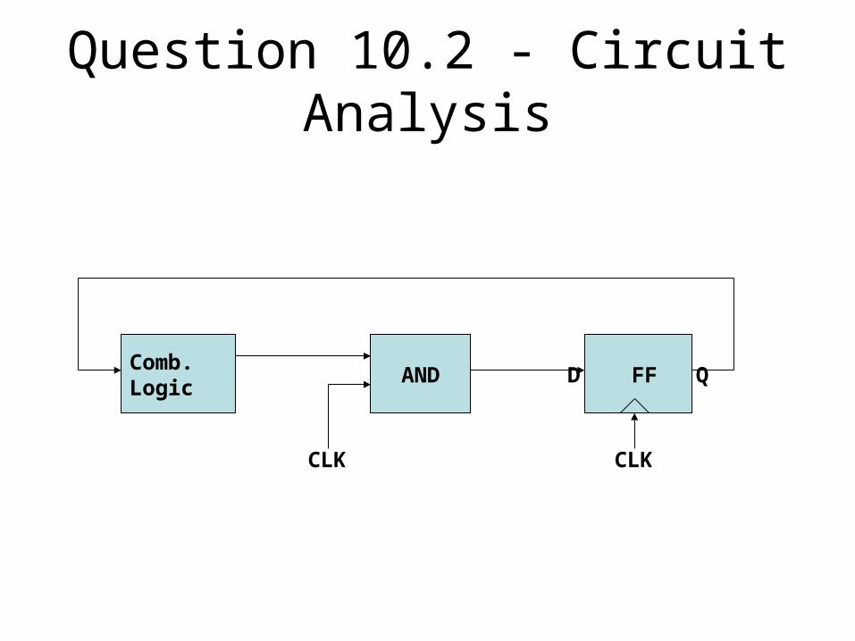
Question 10.2 - Circuit Analysis
Comb.Logic
AND D FF Q
CLKCLK

Question 10.2 - Circuit Analysis
CLK
case #1 – negative setup time
ti-1 ti
Ci
)()(,max 1 ANDpdGpdttttt pdiisui
Logic
Q
D
Not stable Stable

Question 10.2 - Circuit Analysis
CLK
case #1 – negative setup time
ti-1 ti
Ci
)()(,max 1 ANDpdGpdttttt pdiisui
Logic
Q
D
Not stable Stable
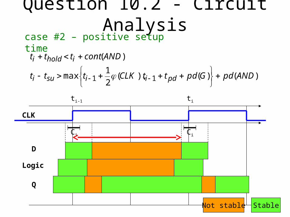
Question 10.2 - Circuit Analysis
CLK
case #2 – positive setup time
ti-1 ti
Ci
Logic
Q
D
Not stable Stable
)()(),(2
1max
)(
11 ANDpdGpdttCLKttt
ANDcontttt
pdiisui
iholdi
Ci

Question 10.2 - Circuit Analysis
CLK
case #2 – positive setup time
ti-1 ti
Ci
Logic
Q
D
Not stable Stable
)()(),(2
1max
)(
11 ANDpdGpdttCLKttt
ANDcontttt
pdiisui
iholdi
Ci

The Marvelous Toy
Toy Design
• Identifying system states
• Identifying state transitions and deciding on Moore or Mealy model
• Detailing the state machine transition and output functions
• The combinational circuits
• The Canonic circuit
• Clock rate calculation

Toy System States
• Only the three switching elements keep state.
• Each has a binary state: Left or Right
• We can model the state of every switch by a single bit.
• Convention: 0=Left, 1=Right
• The total number of states: 23 = 8

State Diagram
000

State Diagram
000
011
100
0/0
1/0
X is LeftZ is LeftY is Left
Enter from LeftOut from LeftSwap X
Enter from RightOut from LeftSwap Y & Z

State Diagram
000
011
100
0/0
1/0 111
0100/0
1/0

State Diagram
000
011
100
0/0
1/0 111
0100/0
1/0
110
001
0/0
1/1
Enter RightOut RightSwap Y&Z

State Diagram
000
011
100
0/0
1/0 111
0100/0
1/0
110
001
0/0
1/1
0/1 1/1

State Diagram
000
011
100
0/0
1/0 111
0100/0
1/0
101
110
001
0/0
1/1
0/1 1/1
0/1
1/1

State Diagram
000
011
100
0/0
1/0 111
0100/0
1/0
101
110
001
0/0
1/1
0/1 1/1
0/1
1/1
0/0
1/1

State Diagram
000
011
100
0/0
1/0 111
0100/0
1/0
101
110
001
0/0
1/1
0/1 1/1
0/1
1/1
0/0
1/10/0
1/1

State Diagram
000
011
100
0/0
1/0 111
0100/0
1/0
101
110
001
0/0
1/1
0/1 1/1
0/1
1/1
0/0
1/1
0/0
1/1
0/01/1

Output Function
Y=0I=0
Y=0I=1
Y=1I=1
Y=1I=0
X=0Z=0
0 0 1 0
X=0Z=1
0 1 1 0
X=1Z=1
1 1 1 1
X=1Z=0
0 0 1 0

Output Function
Output = YI + XZ + ZI (This is λ)
• This circuit has 3 AND(2) in parallel, and then an OR(3)
• No NOT gates.
• Delay = D(AND)+2*D(OR)– Assuming we use OR(2) only

The Next State Function of X
000
011
100
0/0
1/0 111
0100/0
1/0
101
110
001
0/0
1/1
0/1 1/1
0/1
1/1
0/0
1/1
0/0
1/1
0/01/1

Next State Function for X
Y=0I=0
Y=0I=1
Y=1I=1
Y=1I=0
X=0Z=0
1 0 0 1
X=0Z=1
1 0 0 1
X=1Z=1
0 1 1 0
X=1Z=0
0 1 1 0

X Next State Function
X = X’I’+XI (This is part of δ)
• This circuit has: – 2 negations in parallel – 2 AND(2) in parallel, – and then an OR(2)
• Delay = D(NOT)+D(AND)+D(OR)

The Canonic Circuit
State Register
Next State Circuitδ
Output Circuitλ
Input {0,1}
Next State {0,1}3State {0,1}3
Output {0,1}

Stripping away the Flip-Flops
Next State Circuitδ
Output Circuitλ
Input {0,1}
Next State {0,1}3State {0,1}3
Output {0,1}
D-portQ-port

Attaching Delay
Next State Circuitpd(δ)
Output Circuitpd(λ)
Input {0,1}
Next State {0,1}3State {0,1}3
Output {0,1}
D-portQ-port
tpd
pd(IN)
setup(OUT)
tsu

Finding the Clock Rate
Next State Circuitpd(δ)
Output Circuitpd(λ)
Input {0,1}
Next State {0,1}3State {0,1}3
Output {0,1}
D-portQ-port
tpd
pd(IN)
setup(OUT)
tsu

The Clock Rate
supd
pd
su
tpdt
OUTsetuppdt
tpdINpd
OUTsetuppdINpd
CLK
)(
)()(
)()(
)()()(
max}{
We are done!