InTech-Chemical Bath Deposited Cds for Cdte and Cu in Ga Se2 Thin Film Solar Cells Processing
Polycrystalline CdS/CdTe solar cells
Al CompaanDistinguished University Professor of Physics, Emeritus
(Lecture for Heben/Ellingson solar cells class)M h 15 2012March 15, 2012
1

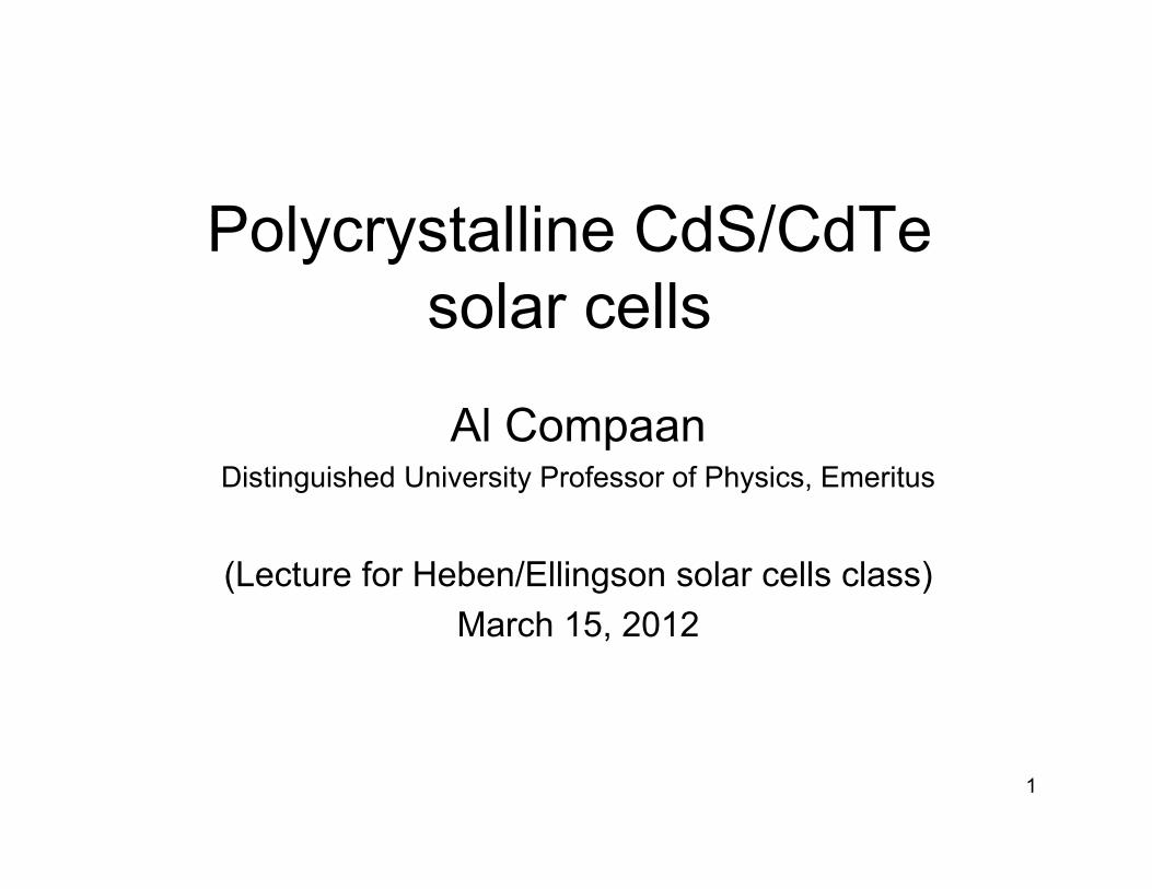
Absorption spectra of various semiconductors
2
actual and attainable single junction cell
efficienciesefficiencies(inorganic materials)
Shockley-Queisser limitShockley Queisser limit (single junction)
Attainable cell efficiencies for AM0 (solid line) and AM1.5 spectra (dashed line) and best efficiencies achieved for several materials as single junctions. (Kazmerski 2006)
3
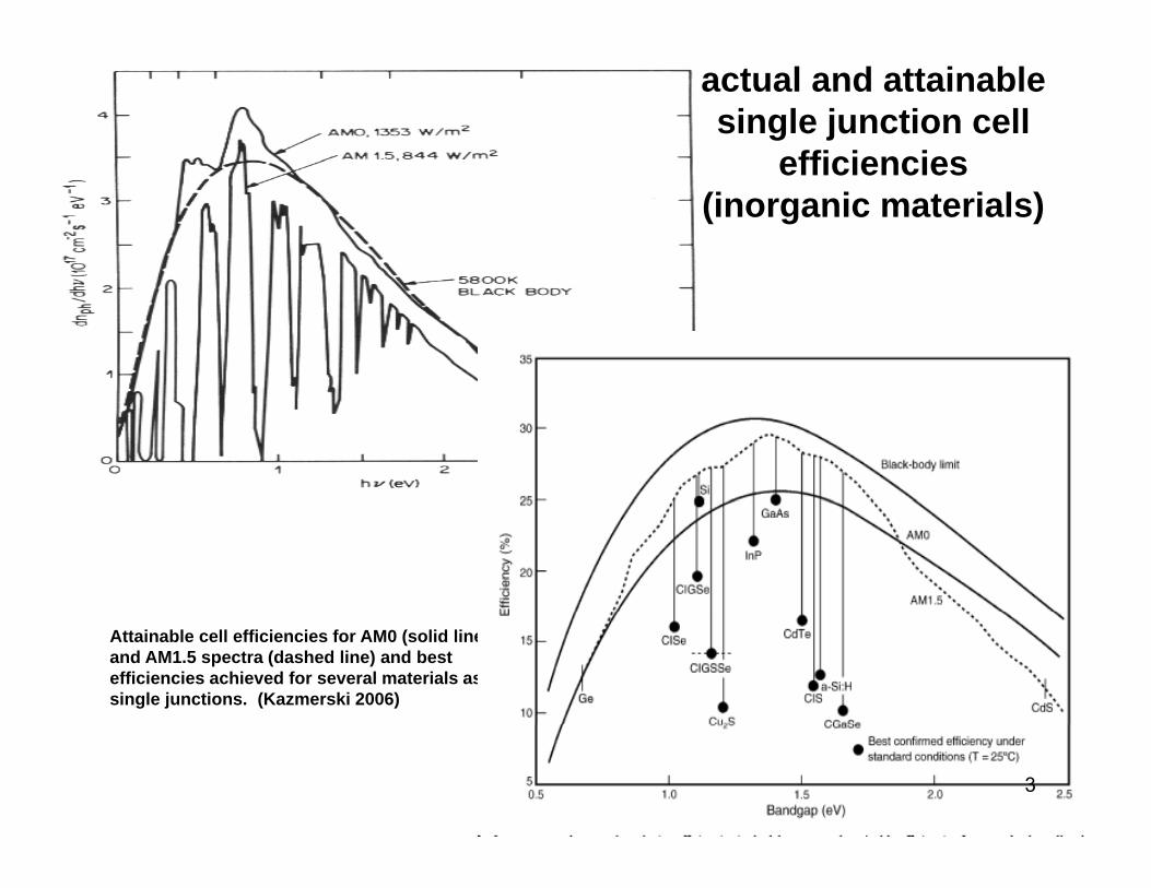
the traditional silicon solar cell
sunlight
the traditional silicon solar cell
metal grid
g
_
transparent conductor
n-type silicont n type silicon
p-type silicon
motor _
+
_ _
+ +
~200 µm
metal electrode
+
4

n-type / p-type BSF
~200 µm~0.3 µm
band diagram for a h j ti ( )
h
|-depletion region-|(space charge region)
|- neutral region -|
homojunction (n on p)• Si (indirect band gap) will have
typically a thick neutral region--
-(space charge region)
e-thermalization
drift
typically a thick neutral region--carrier collection by diffusion
• most thin-film (direct band gap materials) will have mostly field-
EF
CB
VB
drift
drift
assisted collection
+
VB
h-thermalization
drift
Distance across junction
Solar cell structure and energy band diagram showing valence (VB) and conduction bands (CB), Fermi level (EF), photoabsorption, electron-hole pair generation, thermalization,
d d iftand drift. (from Compaan, APS News April, 2005)
5

C-V measurements of depletion width in CdS/CdTe cells
1.0*1015
456789
m-3
) re-annealed
CdTe is difficult to dope p-type
1.0*1014
89
2
3
Con
cent
ratio
n (c
+ -
degraded
extrinsically
2
3
45678
Car
rier C
+ -
1.0 1.5 2.0 2.5
Depletion width
1.0*1013
2
p
Depletion width in a single-sided step junction:W = {(2ΚεoVbi ) / qNa }1/2
(for Si with Na = 1 x 1016 cm-3, W ≈ 0.35 µm)6

Construct a band diagram of the CdS/CdTe solar cell….What information do we need?
Electron affinity of CdTeEa = 4.4 eV
Work functions of common metals
S-H Wei, S.B. Zhang, A. Zunger (T = 0 K band gaps) 7
Band structure?(Construct on board with class discussion)
• Cliff or spike at the CdS/CdTe interface?
• Doping densities in CdTe, in CdS?
• Back barrier for hole transport?
8

UT CdTe sputtered cell on aluminosilicate glass
14.0% efficiency at one-sun illumination
sunlight
aluminosilicate glass
zinc oxidecadmium sulfide
cadmium telluridecadmium telluride
metal
9

From B.E. McCandless and J.R. Sites, PV Handbook, 2002
New record CdTe cell: First Solar, 2011 efficiency = 17.3%
10
New record CdTe cell: First Solar, 2011 efficiency 17.3%(done “on production equipment”)
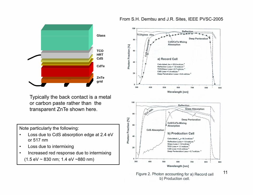
From S.H. Demtsu and J.R. Sites, IEEE PVSC-2005
GlassGlass
TCOHRTCdS
CdTe
ZnTegrid
Typically the back contact is a metal or carbon paste rather than the transparent ZnTe shown heretransparent ZnTe shown here.
Note particularly the following:• Loss due to CdS absorption edge at 2 4 eV• Loss due to CdS absorption edge at 2.4 eV
or 517 nm• Loss due to intermixing• Increased red response due to intermixing
(1 5 eV ~ 830 nm; 1 4 eV ~880 nm)
11
(1.5 eV ~ 830 nm; 1.4 eV ~880 nm)
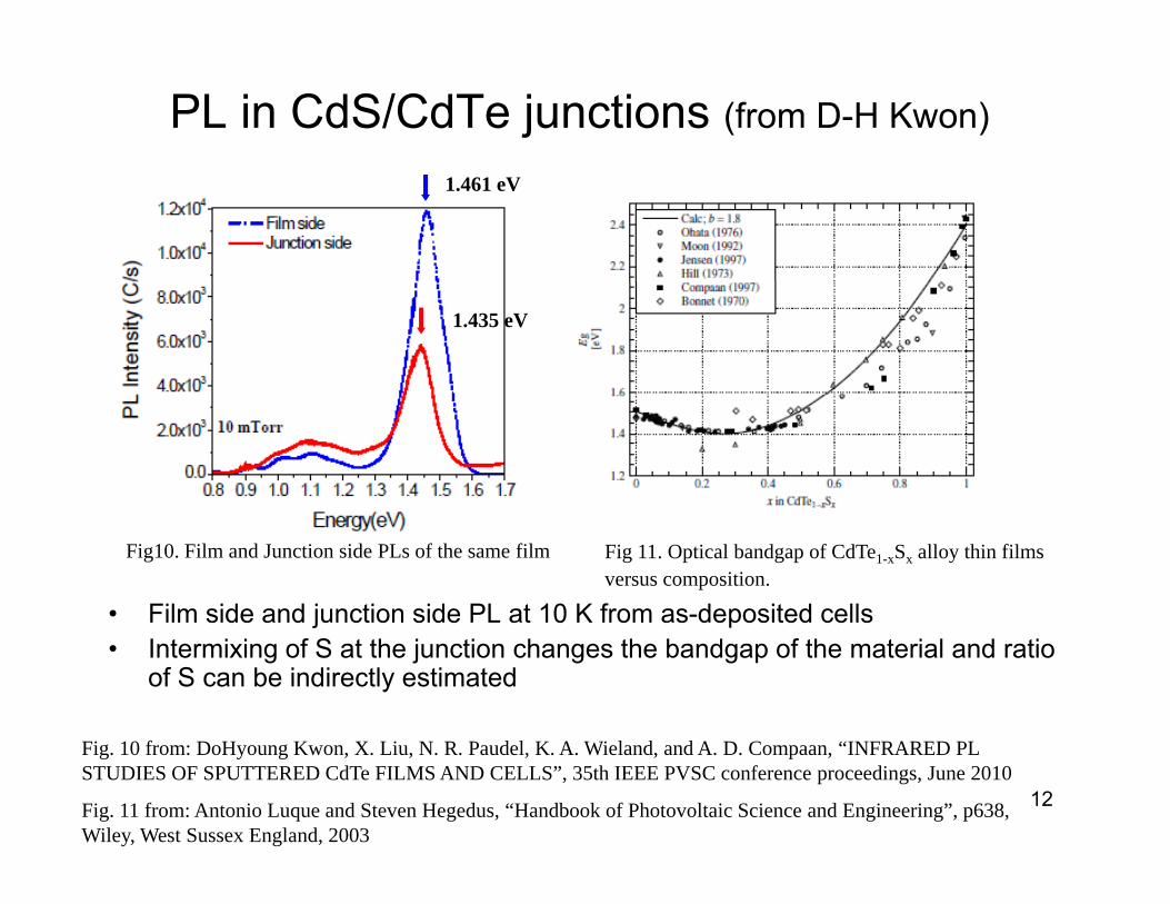
PL in CdS/CdTe junctions (from D-H Kwon)
1.461 eV
1.435 eV
• Film side and junction side PL at 10 K from as-deposited cells
Fig 11. Optical bandgap of CdTe1-xSx alloy thin filmsversus composition.
Fig10. Film and Junction side PLs of the same film
j p• Intermixing of S at the junction changes the bandgap of the material and ratio
of S can be indirectly estimated
Fig. 10 from: DoHyoung Kwon, X. Liu, N. R. Paudel, K. A. Wieland, and A. D. Compaan, “INFRARED PL STUDIES OF SPUTTERED CdTe FILMS AND CELLS”, 35th IEEE PVSC conference proceedings, June 2010
Fig. 11 from: Antonio Luque and Steven Hegedus, “Handbook of Photovoltaic Science and Engineering”, p638, Wiley, West Sussex England, 2003
12

From B.E. McCandless and J.R. Sites, PV Handbook, Chap 14, 2002
13

Calculated impurity levels in CdTey
14
Discuss Cu distributions
• Secondary Ion Mass Spectroscopy(usually done in conjunction with ion beam etching for depth profiling)C i d i th b k t t• Cu is used in the back contact
• CdCl2 “activation” anneal is used just prior to the back contact deposition• CdCl2 activation is done in the presence of O2 at 387 C
15
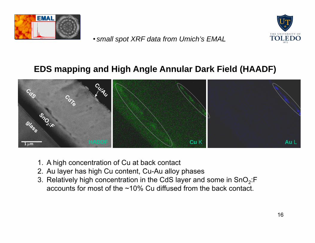
• small spot XRF data from Umich’s EMAL
EDS mapping and High Angle Annular Dark Field (HAADF)
1. A high concentration of Cu at back contact
Au LCu K1 m HADDF
2. Au layer has high Cu content, Cu-Au alloy phases3. Relatively high concentration in the CdS layer and some in SnO2:F
accounts for most of the ~10% Cu diffused from the back contact.
16
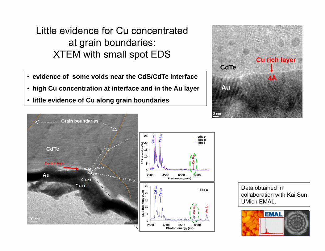
Little evidence for Cu concentrated at grain boundaries: g
XTEM with small spot EDS Cu rich layerCdTe
• evidence of some voids near the CdS/CdTe interfaceAu
evidence of some voids near the CdS/CdTe interface
• high Cu concentration at interface and in the Au layer
• little evidence of Cu along grain boundaries
Grain boundaries
25 eds-eeds-dTe
L
d L
CdTe
A
Cu-rich layer
0
5
10
15
20ED
S in
tens
ity (C
/s) eds-f
Cu
K
TC
Au
15
20
25
ensi
ty (C
/s) eds-a
Cd
L Te
L
2500 4500 6500 8500Photon energy (eV)
Data obtained in collaboration with Kai Sun UMich EMAL.
170
5
10
2500 4500 6500 8500Photon energy (eV)
EDS
inte
Au
L
Cu
K

SIMS profiles of Cu and S in CdTe/CdS(data from Matt Young and Sally Asher (NREL)
• S not present in CdTe before CdCl2 activationS not present in CdTe before CdCl2 activation• Activation produces S-gradient decreasing
from ~1% at the junction• Because of band bowing in the CdSTe
system, S-gradient will yield band bending
18
system, S gradient will yield band bending that should aid electron collection

Plasma dependence on magnetic field
Unbalanced field magnetron
end view side view
Balanced field magnetron
end viewside view
19
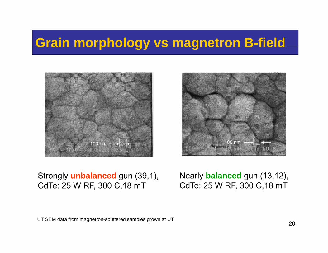
Grain morphology vs magnetron B-fieldGrain morphology vs magnetron B field
100 nm100
Nearly balanced gun (13 12)Strongly unbalanced gun (39 1)
100 nm100 nm
Nearly balanced gun (13,12), CdTe: 25 W RF, 300 C,18 mT
Strongly unbalanced gun (39,1), CdTe: 25 W RF, 300 C,18 mT
20UT SEM data from magnetron-sputtered samples grown at UT
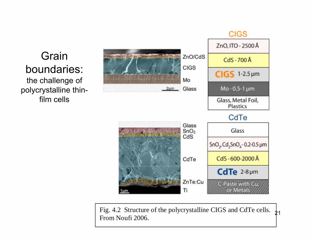
Grain boundaries:the challenge of
polycrystalline thin-film cells
Fig. 4.2 Structure of the polycrystalline CIGS and CdTe cells. From Noufi 2006.
21

EBSD data of grain size and low-angle grain boundaries (Data taken on UT cell SSC548 by Matt Nowell of EDAX-TSL / U. Utah)
( tt d CdT t i CdCl t t d)(sputtered CdTe-center region CdCl2 treated)
secondary electron Image EBSD orientation map
22

Grain size increases with CdCl2 activation: EBSD
SSC 48 C A G
Data from Matt Nowell of EDAX-TSL / U. Utah obtained on UT films
SSC548 Center As-Grown• Grain map and size
distribution including twins (ave grain size = 115 nm)
asas--sputteredsputtered
(ave. grain size = 115 nm)
• Grain map and size distribution excluding twins (Δθ < 5o) (ave grain size =(Δθ < 5 ) (ave. grain size = 176nm)
SSC548 Center CdCl treated
• Grain map and size distribution including twins (ave grain size = 400 nm)
SSC548 Center CdCl2 treated
CdCdCdCd22--activatedactivated
(ave. grain size 400 nm)
• Grain map and size distribution excluding twins (ave grain size = 710 nm)(ave. grain size 710 nm)
23

from cell to module--series integrationseries integration
assembly from smaller cells
monolithic integrationnonconducting substrate
24
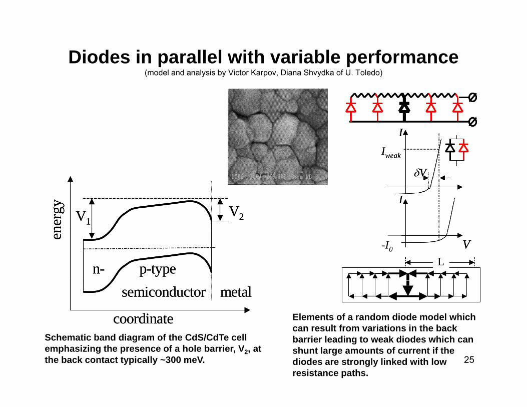
Diodes in parallel with variable performance(model and analysis by Victor Karpov, Diana Shvydka of U. Toledo)( ode a d a a ys s by cto a po , a a S yd a o U o edo)
I
V
Iweak
I
V
Iweak
V1V2
nerg
y
V1V2
nerg
y II
n- p-type
en
n- p-type
en
VL
-I0 VLL
-I0
semiconductor metal
coordinate
semiconductor metal
coordinate Elements of a random diode model which can result from variations in the back
Schematic band diagram of the CdS/CdTe cell emphasizing the presence of a hole barrier, V2, at the back contact typically ~300 meV.
barrier leading to weak diodes which can shunt large amounts of current if the diodes are strongly linked with low resistance paths.
25