Solidification Behavior, Microstructure, Mechanical Properties
Thin Solid Films 517 (2009) 1922–1927
Contents lists available at ScienceDirect
Thin Solid Films
j ourna l homepage: www.e lsev ie r.com/ locate / ts f
Investigation of microstructure and mechanical properties of multi-layerCr/Cr2O3 coatings
Xiaolu Pang a, Kewei Gao a,⁎, Fei Luo a, Yusuf Emirov b, Alexandr A. Levin c, Alex A. Volinsky d
a Department of Materials Physics and Chemistry, University of Science and Technology Beijing, Beijing 100083, Chinab Nanotechnology and Nanomanufacturing Research Center, University of South Florida, Tampa FL 33620, USAc Institut für Strukturphysik, Technische Universität Dresden, 01062 Dresden, Germanyd Department of Mechanical Engineering, University of South Florida, Tampa FL 33620, USA
⁎ Corresponding author.E-mail address: [email protected] (K. Gao).
0040-6090/$ – see front matter © 2008 Elsevier B.V. Adoi:10.1016/j.tsf.2008.10.026
a b s t r a c t
a r t i c l e i n f oArticle history:
Single and multi-layer Cr/C Received 24 January 2008Received in revised form 6 September 2008Accepted 3 October 2008Available online 18 October 2008Keywords:Chromium oxideMulti-layerMicrostructureFracture toughnessAdhesion
r2O3 coatings were deposited by reactive magnetron sputtering with the totalthickness of 7 μm on steel substrates. X-ray diffraction analysis showed that single and multi-layer Cr/Cr2O3
coatings have different preferred crystal orientations. Columnar microstructure was detected by transmissionelectron microscopy both in metal chromium and ceramic chromium oxide layers. Grain size increased withthe coating thickness. The value of single and multi-layer coating's fracture toughness is between 4 and6 MPa·m1/2 measured with the Berkovich tip indentation, and it is between 2.8 and 3.9 MPa·m1/2 whenmeasured with the Vickers indenter. The adhesion is about 192.1 and 246.7 J/m2 for single and multi-layercoatings, respectively.
© 2008 Elsevier B.V. All rights reserved.
1. Introduction
Chromium oxide exhibits good optical, magnetic and mechanicalproperties, so it can be used as a selective solar ray collector and forother applications as a protective coating against wear, corrosion, andoxidation [1–6]. Among various chromium oxides, Cr2O3 is mostchemically stable under ambient conditions [7]. The performanceand reliability of chromium oxide coatings is often limited by theirmechanical properties. Nanoindentation methods are routinely usedfor elastic modulus and hardness coatings characterization, althoughthe main chromium oxide coatings failure model is fracture anddelamination, thus it is important to investigate the coating fracturetoughness and adhesion properties. Up to now, there has been nodiscussion of chromium oxide coatings fracture toughness in theliterature.
Various techniques have been used to deposit Cr2O3 coatings,including sputtering [1,2,4,8–10] electron-beam evaporation [11,12],chemical vapor deposition [6,7], electrochemical deposition [13], andchemical spray pyrolysis [14], based on different applications. Variousdeposition methods result in different chromium oxide coatingsmicrostructure, which controls their properties, so it is important toknow the microstructure of specimens prepared by different deposi-tionmethods. Magnetron sputtering has become the process of choice
ll rights reserved.
for the deposition of a wide range of industrially important coatings.Examples include hard, wear-resistant, low friction, corrosion resis-tant, decorative coatings and coatings with special optical or electricalproperties. Quality films and coatings can be deposited by magnetronsputtering, but unfortunately they are typically highly stressed.With the increase of coating thickness, the residual stress typicallyincreases. Several studies showed that coating thickness plays animportant role in enhancing both physical vapor deposition (PVD)coated tool cutting performance and resistance to abrasive and erosivewear [15]. Graded systems have been employed to obtain thickercoatings without losing performance in terms of coating adhesion andfracture toughness [16]. It is also likely that thicker coatings willimprove corrosion resistance in aqueous environments by eliminatingthrough-thickness pin-hole defects.
In this paper X-ray diffraction (XRD) and transmission electronmicroscopy (TEM) techniques were used to characterize the micro-structure of multi-layer chromiumoxide coatings prepared by reactiveradio frequency magnetron sputtering technique. Fracture toughnessand adhesion were also investigated.
2. Experimental details
Chromium oxide coatings were deposited on W18Cr4V high speedsteel substrates by reactive magnetron sputtering from 50 mm Crtarget (99.95% pure) in Ar/O2 plasma at a total pressure of 10−1 Pa.Distance between the substrate and the target was 55mm. Depositionwas performed in mixed Ar and O2 atmosphere with 350 W radio
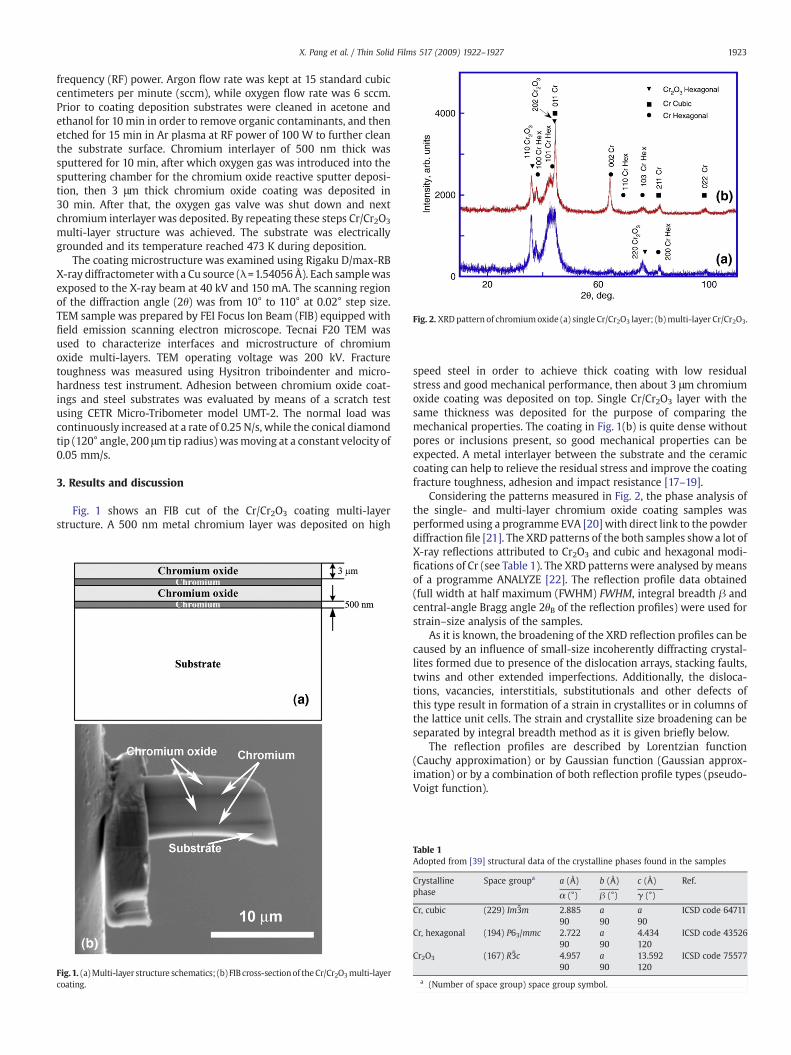
Fig. 2. XRD pattern of chromiumoxide (a) single Cr/Cr2O3 layer; (b)multi-layer Cr/Cr2O3.
1923X. Pang et al. / Thin Solid Films 517 (2009) 1922–1927
frequency (RF) power. Argon flow rate was kept at 15 standard cubiccentimeters per minute (sccm), while oxygen flow rate was 6 sccm.Prior to coating deposition substrates were cleaned in acetone andethanol for 10 min in order to remove organic contaminants, and thenetched for 15 min in Ar plasma at RF power of 100 W to further cleanthe substrate surface. Chromium interlayer of 500 nm thick wassputtered for 10 min, after which oxygen gas was introduced into thesputtering chamber for the chromium oxide reactive sputter deposi-tion, then 3 μm thick chromium oxide coating was deposited in30 min. After that, the oxygen gas valve was shut down and nextchromium interlayer was deposited. By repeating these steps Cr/Cr2O3
multi-layer structure was achieved. The substrate was electricallygrounded and its temperature reached 473 K during deposition.
The coating microstructure was examined using Rigaku D/max-RBX-ray diffractometer with a Cu source (λ=1.54056 Å). Each samplewasexposed to the X-ray beam at 40 kV and 150 mA. The scanning regionof the diffraction angle (2θ) was from 10° to 110° at 0.02° step size.TEM sample was prepared by FEI Focus Ion Beam (FIB) equipped withfield emission scanning electron microscope. Tecnai F20 TEM wasused to characterize interfaces and microstructure of chromiumoxide multi-layers. TEM operating voltage was 200 kV. Fracturetoughness was measured using Hysitron triboindenter and micro-hardness test instrument. Adhesion between chromium oxide coat-ings and steel substrates was evaluated by means of a scratch testusing CETR Micro-Tribometer model UMT-2. The normal load wascontinuously increased at a rate of 0.25 N/s, while the conical diamondtip (120° angle, 200 μm tip radius) wasmoving at a constant velocity of0.05 mm/s.
3. Results and discussion
Fig. 1 shows an FIB cut of the Cr/Cr2O3 coating multi-layerstructure. A 500 nm metal chromium layer was deposited on high
Fig.1. (a)Multi-layer structure schematics; (b) FIB cross-sectionof theCr/Cr2O3multi-layercoating.
speed steel in order to achieve thick coating with low residualstress and good mechanical performance, then about 3 μm chromiumoxide coating was deposited on top. Single Cr/Cr2O3 layer with thesame thickness was deposited for the purpose of comparing themechanical properties. The coating in Fig. 1(b) is quite dense withoutpores or inclusions present, so good mechanical properties can beexpected. A metal interlayer between the substrate and the ceramiccoating can help to relieve the residual stress and improve the coatingfracture toughness, adhesion and impact resistance [17–19].
Considering the patterns measured in Fig. 2, the phase analysis ofthe single- and multi-layer chromium oxide coating samples wasperformed using a programme EVA [20] with direct link to the powderdiffraction file [21]. The XRD patterns of the both samples showa lot ofX-ray reflections attributed to Cr2O3 and cubic and hexagonal modi-fications of Cr (see Table 1). The XRD patterns were analysed by meansof a programme ANALYZE [22]. The reflection profile data obtained(full width at half maximum (FWHM) FWHM, integral breadth β andcentral-angle Bragg angle 2θB of the reflection profiles) were used forstrain–size analysis of the samples.
As it is known, the broadening of the XRD reflection profiles can becaused by an influence of small-size incoherently diffracting crystal-lites formed due to presence of the dislocation arrays, stacking faults,twins and other extended imperfections. Additionally, the disloca-tions, vacancies, interstitials, substitutionals and other defects ofthis type result in formation of a strain in crystallites or in columns ofthe lattice unit cells. The strain and crystallite size broadening can beseparated by integral breadth method as it is given briefly below.
The reflection profiles are described by Lorentzian function(Cauchy approximation) or by Gaussian function (Gaussian approx-imation) or by a combination of both reflection profile types (pseudo-Voigt function).
Table 1Adopted from [39] structural data of the crystalline phases found in the samples
Crystallinephase
Space groupa a (Å) b (Å) c (Å) Ref.
α (°) β (°) γ (°)
Cr, cubic (229) Im3̄m 2.885 a a ICSD code 6471190 90 90
Cr, hexagonal (194) P63/mmc 2.722 a 4.434 ICSD code 4352690 90 120
Cr2O3 (167) R3̄c 4.957 a 13.592 ICSD code 7557790 90 120
a (Number of space group) space group symbol.
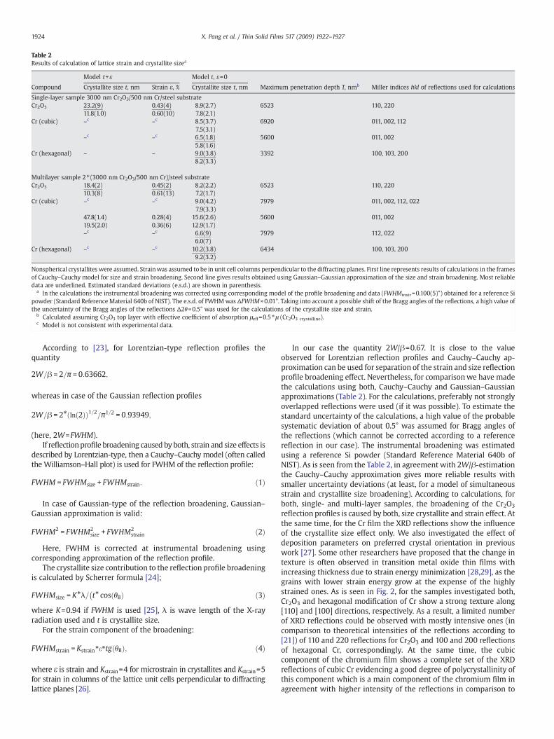
Table 2Results of calculation of lattice strain and crystallite sizea
Model t+ε Model t, ε=0
Compound Crystallite size t, nm Strain ε, % Crystallite size t, nm Maximum penetration depth T, nmb Miller indices hkl of reflections used for calculations
Single-layer sample 3000 nm Cr2O3/500 nm Cr/steel substrateCr2O3 23.2(9) 0.43(4) 8.9(2.7) 6523 110, 220
11.8(1.0) 0.60(10) 7.8(2.1)Cr (cubic) –c –c 8.5(3.7) 6920 011, 002, 112
7.5(3.1)–c –c 6.5(1.8) 5600 011, 002
5.8(1.6)Cr (hexagonal) – – 9.0(3.8) 3392 100, 103, 200
8.2(3.3)
Multilayer sample 2⁎ (3000 nm Cr2O3/500 nm Cr)/steel substrateCr2O3 18.4(2) 0.45(2) 8.2(2.2) 6523 110, 220
10.3(8) 0.61(13) 7.2(1.7)Cr (cubic) –c –c 9.0(4.2) 7979 011, 002, 112, 022
7.9(3.3)47.8(1.4) 0.28(4) 15.6(2.6) 5600 011, 00219.5(2.0) 0.36(6) 12.9(1.7)–c –c 6.6(9) 7979 112, 022
6.0(7)Cr (hexagonal) –c –c 10.2(3.8) 6434 100, 103, 200
9.2(3.2)
Nonspherical crystallites were assumed. Strainwas assumed to be in unit cell columns perpendicular to the diffracting planes. First line represents results of calculations in the framesof Cauchy–Cauchy model for size and strain broadening. Second line gives results obtained using Gaussian–Gaussian approximation of the size and strain broadening. Most reliabledata are underlined. Estimated standard deviations (e.s.d.) are shown in parenthesis.
a In the calculations the instrumental broadening was corrected using corresponding model of the profile broadening and data (FWHMinstr=0.100(5)°) obtained for a reference Sipowder (Standard Reference Material 640b of NIST). The e.s.d. of FWHMwas ΔFWHM≈0.01°. Taking into account a possible shift of the Bragg angles of the reflections, a high value ofthe uncertainty of the Bragg angles of the reflections Δ2θ=0.5° was used for the calculations of the crystallite size and strain.
b Calculated assuming Cr2O3 top layer with effective coefficient of absorption μeff =0.5⁎μ (Cr2O3 crystalline).c Model is not consistent with experimental data.
1924 X. Pang et al. / Thin Solid Films 517 (2009) 1922–1927
According to [23], for Lorentzian-type reflection profiles thequantity
2W=β = 2=π = 0:63662;
whereas in case of the Gaussian reflection profiles
2W=β = 2T ln 2ð Þð Þ1=2=π1=2 = 0:93949;
(here, 2W=FWHM).If reflectionprofile broadening caused by both, strain and size effects is
described by Lorentzian-type, then a Cauchy–Cauchy model (often calledthe Williamson–Hall plot) is used for FWHM of the reflection profile:
FWHM = FWHMsize + FWHMstrain: ð1Þ
In case of Gaussian-type of the reflection broadening, Gaussian–Gaussian approximation is valid:
FWHM2 = FWHM2size + FWHM2
strain ð2Þ
Here, FWHM is corrected at instrumental broadening usingcorresponding approximation of the reflection profile.
The crystallite size contribution to the reflection profile broadeningis calculated by Scherrer formula [24];
FWHMsize = KTλ= tT cos θBð Þ� ð3Þwhere K=0.94 if FWHM is used [25], λ is wave length of the X-rayradiation used and t is crystallite size.
For the strain component of the broadening:
FWHMstrain = KstrainTeTtg θBð Þ; ð4Þ
where ε is strain and Kstrain=4 for microstrain in crystallites and Kstrain=5for strain in columns of the lattice unit cells perpendicular to diffractinglattice planes [26].
In our case the quantity 2W/β=0.67. It is close to the valueobserved for Lorentzian reflection profiles and Cauchy–Cauchy ap-proximation can be used for separation of the strain and size reflectionprofile broadening effect. Nevertheless, for comparisonwe have madethe calculations using both, Cauchy–Cauchy and Gaussian–Gaussianapproximations (Table 2). For the calculations, preferably not stronglyoverlapped reflections were used (if it was possible). To estimate thestandard uncertainty of the calculations, a high value of the probablesystematic deviation of about 0.5° was assumed for Bragg angles ofthe reflections (which cannot be corrected according to a referencereflection in our case). The instrumental broadening was estimatedusing a reference Si powder (Standard Reference Material 640b ofNIST). As is seen from the Table 2, in agreement with 2W/β-estimationthe Cauchy–Cauchy approximation gives more reliable results withsmaller uncertainty deviations (at least, for a model of simultaneousstrain and crystallite size broadening). According to calculations, forboth, single- and multi-layer samples, the broadening of the Cr2O3
reflection profiles is caused by both, size crystallite and strain effect. Atthe same time, for the Cr film the XRD reflections show the influenceof the crystallite size effect only. We also investigated the effect ofdeposition parameters on preferred crystal orientation in previouswork [27]. Some other researchers have proposed that the change intexture is often observed in transition metal oxide thin films withincreasing thickness due to strain energy minimization [28,29], as thegrains with lower strain energy grow at the expense of the highlystrained ones. As is seen in Fig. 2, for the samples investigated both,Cr2O3 and hexagonal modification of Cr show a strong texture along[110] and [100] directions, respectively. As a result, a limited numberof XRD reflections could be observed with mostly intensive ones (incomparison to theoretical intensities of the reflections according to[21]) of 110 and 220 reflections for Cr2O3 and 100 and 200 reflectionsof hexagonal Cr, correspondingly. At the same time, the cubiccomponent of the chromium film shows a complete set of the XRDreflections of cubic Cr evidencing a good degree of polycrystallinity ofthis component which is a main component of the chromium film inagreement with higher intensity of the reflections in comparison to
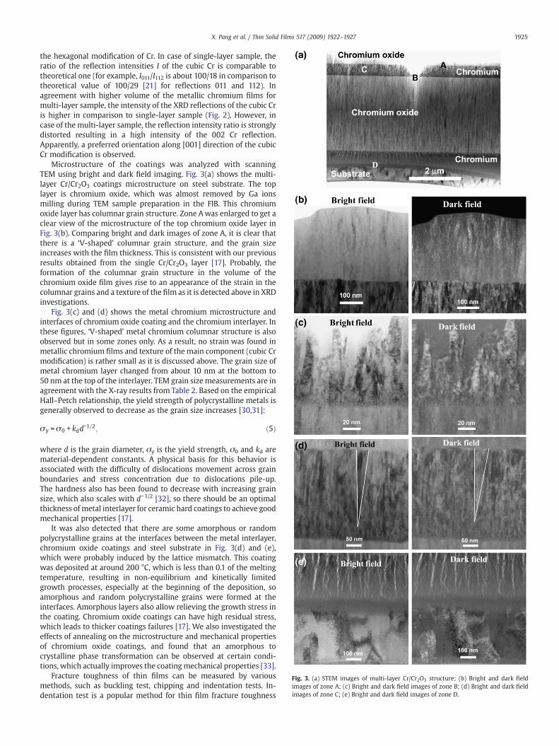
Fig. 3. (a) STEM images of multi-layer Cr/Cr2O3 structure; (b) Bright and dark fieldimages of zone A; (c) Bright and dark field images of zone B; (d) Bright and dark fieldimages of zone C; (e) Bright and dark field images of zone D.
1925X. Pang et al. / Thin Solid Films 517 (2009) 1922–1927
the hexagonal modification of Cr. In case of single-layer sample, theratio of the reflection intensities I of the cubic Cr is comparable totheoretical one (for example, I011/I112 is about 100/18 in comparison totheoretical value of 100/29 [21] for reflections 011 and 112). Inagreement with higher volume of the metallic chromium films formulti-layer sample, the intensity of the XRD reflections of the cubic Cris higher in comparison to single-layer sample (Fig. 2). However, incase of the multi-layer sample, the reflection intensity ratio is stronglydistorted resulting in a high intensity of the 002 Cr reflection.Apparently, a preferred orientation along [001] direction of the cubicCr modification is observed.
Microstructure of the coatings was analyzed with scanningTEM using bright and dark field imaging. Fig. 3(a) shows the multi-layer Cr/Cr2O3 coatings microstructure on steel substrate. The toplayer is chromium oxide, which was almost removed by Ga ionsmilling during TEM sample preparation in the FIB. This chromiumoxide layer has columnar grain structure. Zone Awas enlarged to get aclear view of the microstructure of the top chromium oxide layer inFig. 3(b). Comparing bright and dark images of zone A, it is clear thatthere is a ‘V-shaped’ columnar grain structure, and the grain sizeincreases with the film thickness. This is consistent with our previousresults obtained from the single Cr/Cr2O3 layer [17]. Probably, theformation of the columnar grain structure in the volume of thechromium oxide film gives rise to an appearance of the strain in thecolumnar grains and a texture of the film as it is detected above in XRDinvestigations.
Fig. 3(c) and (d) shows the metal chromium microstructure andinterfaces of chromium oxide coating and the chromium interlayer. Inthese figures, ‘V-shaped’ metal chromium columnar structure is alsoobserved but in some zones only. As a result, no strain was found inmetallic chromium films and texture of the main component (cubic Crmodification) is rather small as it is discussed above. The grain size ofmetal chromium layer changed from about 10 nm at the bottom to50 nm at the top of the interlayer. TEM grain size measurements are inagreement with the X-ray results from Table 2. Based on the empiricalHall–Petch relationship, the yield strength of polycrystalline metals isgenerally observed to decrease as the grain size increases [30,31]:
σy = σ0 + kdd−1=2; ð5Þ
where d is the grain diameter, σy is the yield strength, σ0 and kd arematerial-dependent constants. A physical basis for this behavior isassociated with the difficulty of dislocations movement across grainboundaries and stress concentration due to dislocations pile-up.The hardness also has been found to decrease with increasing grainsize, which also scales with d−1/2 [32], so there should be an optimalthickness of metal interlayer for ceramic hard coatings to achieve goodmechanical properties [17].
It was also detected that there are some amorphous or randompolycrystalline grains at the interfaces between the metal interlayer,chromium oxide coatings and steel substrate in Fig. 3(d) and (e),which were probably induced by the lattice mismatch. This coatingwas deposited at around 200 °C, which is less than 0.1 of the meltingtemperature, resulting in non-equilibrium and kinetically limitedgrowth processes, especially at the beginning of the deposition, soamorphous and random polycrystalline grains were formed at theinterfaces. Amorphous layers also allow relieving the growth stress inthe coating. Chromium oxide coatings can have high residual stress,which leads to thicker coatings failures [17]. We also investigated theeffects of annealing on the microstructure and mechanical propertiesof chromium oxide coatings, and found that an amorphous tocrystalline phase transformation can be observed at certain condi-tions, which actually improves the coatingmechanical properties [33].
Fracture toughness of thin films can be measured by variousmethods, such as buckling test, chipping and indentation tests. In-dentation test is a popular method for thin film fracture toughness
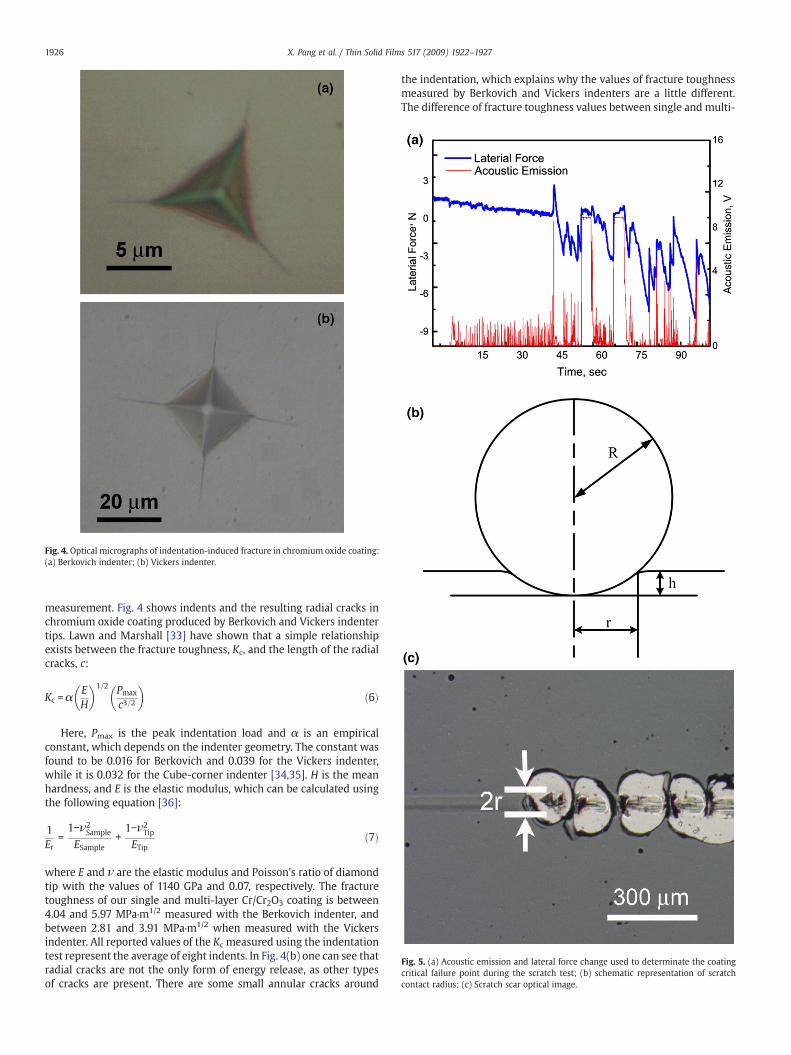
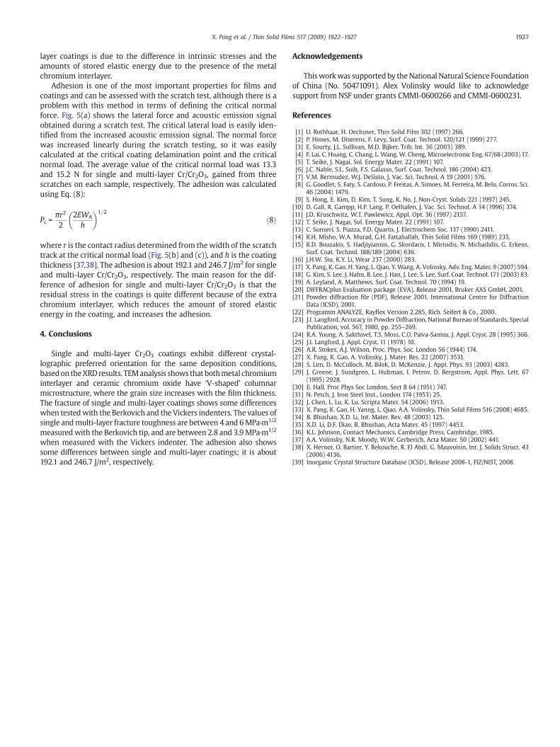
Fig. 5. (a) Acoustic emission and lateral force change used to determinate the coatingcritical failure point during the scratch test; (b) schematic representation of scratchcontact radius; (c) Scratch scar optical image.
Fig. 4. Optical micrographs of indentation-induced fracture in chromium oxide coating:(a) Berkovich indenter; (b) Vickers indenter.
1926 X. Pang et al. / Thin Solid Films 517 (2009) 1922–1927
measurement. Fig. 4 shows indents and the resulting radial cracks inchromium oxide coating produced by Berkovich and Vickers indentertips. Lawn and Marshall [33] have shown that a simple relationshipexists between the fracture toughness, Kc, and the length of the radialcracks, c:
Kc = αEH
� �1=2 Pmax
c3=2
� �ð6Þ
Here, Pmax is the peak indentation load and α is an empiricalconstant, which depends on the indenter geometry. The constant wasfound to be 0.016 for Berkovich and 0.039 for the Vickers indenter,while it is 0.032 for the Cube-corner indenter [34,35]. H is the meanhardness, and E is the elastic modulus, which can be calculated usingthe following equation [36]:
1Er
=1−ν2
Sample
ESample+1−ν2
Tip
ETipð7Þ
where E and ν are the elastic modulus and Poisson's ratio of diamondtip with the values of 1140 GPa and 0.07, respectively. The fracturetoughness of our single and multi-layer Cr/Cr2O3 coating is between4.04 and 5.97 MPa·m1/2 measured with the Berkovich indenter, andbetween 2.81 and 3.91 MPa·m1/2 when measured with the Vickersindenter. All reported values of the Kc measured using the indentationtest represent the average of eight indents. In Fig. 4(b) one can see thatradial cracks are not the only form of energy release, as other typesof cracks are present. There are some small annular cracks around
the indentation, which explains why the values of fracture toughnessmeasured by Berkovich and Vickers indenters are a little different.The difference of fracture toughness values between single and multi-
1927X. Pang et al. / Thin Solid Films 517 (2009) 1922–1927
layer coatings is due to the difference in intrinsic stresses and theamounts of stored elastic energy due to the presence of the metalchromium interlayer.
Adhesion is one of the most important properties for films andcoatings and can be assessed with the scratch test, although there is aproblem with this method in terms of defining the critical normalforce. Fig. 5(a) shows the lateral force and acoustic emission signalobtained during a scratch test. The critical lateral load is easily iden-tified from the increased acoustic emission signal. The normal forcewas increased linearly during the scratch testing, so it was easilycalculated at the critical coating delamination point and the criticalnormal load. The average value of the critical normal load was 13.3and 15.2 N for single and multi-layer Cr/Cr2O3, gained from threescratches on each sample, respectively. The adhesion was calculatedusing Eq. (8):
Pc =πr2
22EWA
h
� �1=2
ð8Þ
where r is the contact radius determined from thewidth of the scratchtrack at the critical normal load (Fig. 5(b) and (c)), and h is the coatingthickness [37,38]. The adhesion is about 192.1 and 246.7 J/m2 for singleand multi-layer Cr/Cr2O3, respectively. The main reason for the dif-ference of adhesion for single and multi-layer Cr/Cr2O3 is that theresidual stress in the coatings is quite different because of the extrachromium interlayer, which reduces the amount of stored elasticenergy in the coating, and increases the adhesion.
4. Conclusions
Single and multi-layer Cr2O3 coatings exhibit different crystal-lographic preferred orientation for the same deposition conditions,basedon theXRDresults. TEManalysis shows that bothmetal chromiuminterlayer and ceramic chromium oxide have ‘V-shaped’ columnarmicrostructure, where the grain size increases with the film thickness.The fracture of single and multi-layer coatings shows some differenceswhen testedwith the Berkovich and the Vickers indenters. The values ofsingle andmulti-layer fracture toughness are between 4 and 6MPa·m1/2
measuredwith the Berkovich tip, and are between 2.8 and 3.9MPa·m1/2
when measured with the Vickers indenter. The adhesion also showssome differences between single and multi-layer coatings; it is about192.1 and 246.7 J/m2, respectively.
Acknowledgements
Thisworkwas supportedby theNational Natural Science Foundationof China (No. 50471091). Alex Volinsky would like to acknowledgesupport from NSF under grants CMMI-0600266 and CMMI-0600231.
References
[1] U. Rothhaar, H. Oechsner, Thin Solid Film 302 (1997) 266.[2] P. Hones, M. Diserens, F. Levy, Surf. Coat. Technol. 120/121 (1999) 277.[3] E. Sourty, J.L. Sullivan, M.D. Bijker, Trib. Int. 36 (2003) 389.[4] F. Lai, C. Huang, C. Chang, L. Wang, W. Cheng, Microelectronic Eng. 67/68 (2003) 17.[5] T. Seike, J. Nagai, Sol. Energy Mater. 22 (1991) 107.[6] J.C. Nable, S.L. Suib, F.S. Galasso, Surf. Coat. Technol. 186 (2004) 423.[7] V.M. Bermudez, W.J. DeSisto, J. Vac. Sci. Technol. A 19 (2001) 576.[8] G. Goodlet, S. Faty, S. Cardoso, P. Freitas, A. Simoes, M. Ferreira, M. Belo, Corros. Sci.
46 (2004) 1479.[9] S. Hong, E. Kim, D. Kim, T. Sung, K. No, J. Non-Cryst. Solids 221 (1997) 245.[10] D. Gall, R. Gampp, H.P. Lang, P. Oelhafen, J. Vac. Sci. Technol. A 14 (1996) 374.[11] J.D. Kruschwitz, W.T. Pawlewicz, Appl. Opt. 36 (1997) 2157.[12] T. Seike, J. Nagai, Sol. Energy Mater. 22 (1991) 107.[13] C. Sunseri, S. Piazza, F.D. Quarto, J. Electrochem Soc. 137 (1990) 2411.[14] R.H. Misho, W.A. Murad, G.H. Fattahallah, Thin Solid Films 169 (1989) 235.[15] K.D. Bouzakis, S. Hadjiyiannis, G. Skordaris, I. Mirisidis, N. Michailidis, G. Erkens,
Surf. Coat. Technol. 188/189 (2004) 636.[16] J.H.W. Siu, K.Y. Li, Wear 237 (2000) 283.[17] X. Pang, K. Gao, H. Yang, L. Qiao, Y.Wang, A. Volinsky, Adv. Eng. Mater. 9 (2007) 594.[18] G. Kim, S. Lee, J. Hahn, B. Lee, J. Han, J. Lee, S. Lee, Surf. Coat. Technol. 171 (2003) 83.[19] A. Leyland, A. Matthews, Surf. Coat. Technol. 70 (1994) 19.[20] DIFFRACplus Evaluation package (EVA), Release 2001, Bruker AXS GmbH, 2001.[21] Powder diffraction file (PDF), Release 2001, International Centre for Diffraction
Data (ICSD), 2001.[22] Programm ANALYZE, Rayflex Version 2.285, Rich. Seifert & Co., 2000.[23] J.I. Langford, Accuracy in Powder Diffraction, National Bureau of Standards, Special
Publication, vol. 567, 1980, pp. 255–269.[24] R.A. Young, A. Sakthivel, T.S. Moss, C.O. Paiva-Santos, J. Appl. Cryst. 28 (1995) 366.[25] J.I. Langford, J. Appl. Cryst. 11 (1978) 10.[26] A.R. Stokes, A.J. Wilson, Proc. Phys. Soc. London 56 (1944) 174.[27] X. Pang, K. Gao, A. Volinsky, J. Mater. Res. 22 (2007) 3531.[28] S. Lim, D. McCulloch, M. Bilek, D. McKenzie, J. Appl. Phys. 93 (2003) 4283.[29] J. Greene, J. Sundgren, L. Hultman, I. Petrov, D. Bergstrom, Appl. Phys. Lett. 67
(1995) 2928.[30] E. Hall, Proc Phys Soc London, Sect B 64 (1951) 747.[31] N. Petch, J. Iron Steel Inst., London 174 (1953) 25.[32] J. Chen, L. Lu, K. Lu. Scripta Mater. 54 (2006) 1913.[33] X. Pang, K. Gao, H. Yanng, L. Qiao, A.A. Volinsky, Thin Solid Films 516 (2008) 4685.[34] B. Bhushan, X.D. Li, Int. Mater. Rev. 48 (2003) 125.[35] X.D. Li, D.F. Diao, B. Bhushan, Acta Mater. 45 (1997) 4453.[36] K.L. Johnson, Contact Mechanics, Cambridge Press, Cambridge, 1985.[37] A.A. Volinsky, N.R. Moody, W.W. Gerberich, Acta Mater. 50 (2002) 441.[38] X. Hernot, O. Bartier, Y. Bekouche, R. El Abdi, G. Mauvoisin, Int. J. Solids Struct. 43
(2006) 4136.[39] Inorganic Crystal Structure Database (ICSD), Release 2008-1, FIZ/NIST, 2008.